WO2014123173A1 - Dc-dcコンバータ - Google Patents
Dc-dcコンバータ Download PDFInfo
- Publication number
- WO2014123173A1 WO2014123173A1 PCT/JP2014/052715 JP2014052715W WO2014123173A1 WO 2014123173 A1 WO2014123173 A1 WO 2014123173A1 JP 2014052715 W JP2014052715 W JP 2014052715W WO 2014123173 A1 WO2014123173 A1 WO 2014123173A1
- Authority
- WO
- WIPO (PCT)
- Prior art keywords
- voltage
- circuit
- current
- switching
- smoothing
- Prior art date
- Legal status (The legal status is an assumption and is not a legal conclusion. Google has not performed a legal analysis and makes no representation as to the accuracy of the status listed.)
- Ceased
Links
Images





Classifications
-
- H—ELECTRICITY
- H02—GENERATION; CONVERSION OR DISTRIBUTION OF ELECTRIC POWER
- H02M—APPARATUS FOR CONVERSION BETWEEN AC AND AC, BETWEEN AC AND DC, OR BETWEEN DC AND DC, AND FOR USE WITH MAINS OR SIMILAR POWER SUPPLY SYSTEMS; CONVERSION OF DC OR AC INPUT POWER INTO SURGE OUTPUT POWER; CONTROL OR REGULATION THEREOF
- H02M3/00—Conversion of DC power input into DC power output
- H02M3/02—Conversion of DC power input into DC power output without intermediate conversion into AC
- H02M3/04—Conversion of DC power input into DC power output without intermediate conversion into AC by static converters
- H02M3/10—Conversion of DC power input into DC power output without intermediate conversion into AC by static converters using discharge tubes with control electrode or semiconductor devices with control electrode
- H02M3/145—Conversion of DC power input into DC power output without intermediate conversion into AC by static converters using discharge tubes with control electrode or semiconductor devices with control electrode using devices of a triode or transistor type requiring continuous application of a control signal
- H02M3/155—Conversion of DC power input into DC power output without intermediate conversion into AC by static converters using discharge tubes with control electrode or semiconductor devices with control electrode using devices of a triode or transistor type requiring continuous application of a control signal using semiconductor devices only
- H02M3/156—Conversion of DC power input into DC power output without intermediate conversion into AC by static converters using discharge tubes with control electrode or semiconductor devices with control electrode using devices of a triode or transistor type requiring continuous application of a control signal using semiconductor devices only with automatic control of output voltage or current, e.g. switching regulators
-
- H—ELECTRICITY
- H02—GENERATION; CONVERSION OR DISTRIBUTION OF ELECTRIC POWER
- H02M—APPARATUS FOR CONVERSION BETWEEN AC AND AC, BETWEEN AC AND DC, OR BETWEEN DC AND DC, AND FOR USE WITH MAINS OR SIMILAR POWER SUPPLY SYSTEMS; CONVERSION OF DC OR AC INPUT POWER INTO SURGE OUTPUT POWER; CONTROL OR REGULATION THEREOF
- H02M3/00—Conversion of DC power input into DC power output
- H02M3/02—Conversion of DC power input into DC power output without intermediate conversion into AC
- H02M3/04—Conversion of DC power input into DC power output without intermediate conversion into AC by static converters
- H02M3/10—Conversion of DC power input into DC power output without intermediate conversion into AC by static converters using discharge tubes with control electrode or semiconductor devices with control electrode
- H02M3/145—Conversion of DC power input into DC power output without intermediate conversion into AC by static converters using discharge tubes with control electrode or semiconductor devices with control electrode using devices of a triode or transistor type requiring continuous application of a control signal
- H02M3/155—Conversion of DC power input into DC power output without intermediate conversion into AC by static converters using discharge tubes with control electrode or semiconductor devices with control electrode using devices of a triode or transistor type requiring continuous application of a control signal using semiconductor devices only
-
- H—ELECTRICITY
- H02—GENERATION; CONVERSION OR DISTRIBUTION OF ELECTRIC POWER
- H02M—APPARATUS FOR CONVERSION BETWEEN AC AND AC, BETWEEN AC AND DC, OR BETWEEN DC AND DC, AND FOR USE WITH MAINS OR SIMILAR POWER SUPPLY SYSTEMS; CONVERSION OF DC OR AC INPUT POWER INTO SURGE OUTPUT POWER; CONTROL OR REGULATION THEREOF
- H02M3/00—Conversion of DC power input into DC power output
- H02M3/02—Conversion of DC power input into DC power output without intermediate conversion into AC
- H02M3/04—Conversion of DC power input into DC power output without intermediate conversion into AC by static converters
- H02M3/10—Conversion of DC power input into DC power output without intermediate conversion into AC by static converters using discharge tubes with control electrode or semiconductor devices with control electrode
- H02M3/145—Conversion of DC power input into DC power output without intermediate conversion into AC by static converters using discharge tubes with control electrode or semiconductor devices with control electrode using devices of a triode or transistor type requiring continuous application of a control signal
- H02M3/155—Conversion of DC power input into DC power output without intermediate conversion into AC by static converters using discharge tubes with control electrode or semiconductor devices with control electrode using devices of a triode or transistor type requiring continuous application of a control signal using semiconductor devices only
- H02M3/156—Conversion of DC power input into DC power output without intermediate conversion into AC by static converters using discharge tubes with control electrode or semiconductor devices with control electrode using devices of a triode or transistor type requiring continuous application of a control signal using semiconductor devices only with automatic control of output voltage or current, e.g. switching regulators
- H02M3/158—Conversion of DC power input into DC power output without intermediate conversion into AC by static converters using discharge tubes with control electrode or semiconductor devices with control electrode using devices of a triode or transistor type requiring continuous application of a control signal using semiconductor devices only with automatic control of output voltage or current, e.g. switching regulators including plural semiconductor devices as final control devices for a single load
-
- H—ELECTRICITY
- H02—GENERATION; CONVERSION OR DISTRIBUTION OF ELECTRIC POWER
- H02M—APPARATUS FOR CONVERSION BETWEEN AC AND AC, BETWEEN AC AND DC, OR BETWEEN DC AND DC, AND FOR USE WITH MAINS OR SIMILAR POWER SUPPLY SYSTEMS; CONVERSION OF DC OR AC INPUT POWER INTO SURGE OUTPUT POWER; CONTROL OR REGULATION THEREOF
- H02M3/00—Conversion of DC power input into DC power output
- H02M3/02—Conversion of DC power input into DC power output without intermediate conversion into AC
- H02M3/04—Conversion of DC power input into DC power output without intermediate conversion into AC by static converters
- H02M3/10—Conversion of DC power input into DC power output without intermediate conversion into AC by static converters using discharge tubes with control electrode or semiconductor devices with control electrode
- H02M3/145—Conversion of DC power input into DC power output without intermediate conversion into AC by static converters using discharge tubes with control electrode or semiconductor devices with control electrode using devices of a triode or transistor type requiring continuous application of a control signal
- H02M3/155—Conversion of DC power input into DC power output without intermediate conversion into AC by static converters using discharge tubes with control electrode or semiconductor devices with control electrode using devices of a triode or transistor type requiring continuous application of a control signal using semiconductor devices only
- H02M3/156—Conversion of DC power input into DC power output without intermediate conversion into AC by static converters using discharge tubes with control electrode or semiconductor devices with control electrode using devices of a triode or transistor type requiring continuous application of a control signal using semiconductor devices only with automatic control of output voltage or current, e.g. switching regulators
- H02M3/158—Conversion of DC power input into DC power output without intermediate conversion into AC by static converters using discharge tubes with control electrode or semiconductor devices with control electrode using devices of a triode or transistor type requiring continuous application of a control signal using semiconductor devices only with automatic control of output voltage or current, e.g. switching regulators including plural semiconductor devices as final control devices for a single load
- H02M3/1584—Conversion of DC power input into DC power output without intermediate conversion into AC by static converters using discharge tubes with control electrode or semiconductor devices with control electrode using devices of a triode or transistor type requiring continuous application of a control signal using semiconductor devices only with automatic control of output voltage or current, e.g. switching regulators including plural semiconductor devices as final control devices for a single load with a plurality of power processing stages connected in parallel
-
- H—ELECTRICITY
- H02—GENERATION; CONVERSION OR DISTRIBUTION OF ELECTRIC POWER
- H02M—APPARATUS FOR CONVERSION BETWEEN AC AND AC, BETWEEN AC AND DC, OR BETWEEN DC AND DC, AND FOR USE WITH MAINS OR SIMILAR POWER SUPPLY SYSTEMS; CONVERSION OF DC OR AC INPUT POWER INTO SURGE OUTPUT POWER; CONTROL OR REGULATION THEREOF
- H02M3/00—Conversion of DC power input into DC power output
- H02M3/22—Conversion of DC power input into DC power output with intermediate conversion into AC
- H02M3/24—Conversion of DC power input into DC power output with intermediate conversion into AC by static converters
- H02M3/28—Conversion of DC power input into DC power output with intermediate conversion into AC by static converters using discharge tubes with control electrode or semiconductor devices with control electrode to produce the intermediate AC
- H02M3/285—Single converters with a plurality of output stages connected in parallel
-
- H—ELECTRICITY
- H02—GENERATION; CONVERSION OR DISTRIBUTION OF ELECTRIC POWER
- H02M—APPARATUS FOR CONVERSION BETWEEN AC AND AC, BETWEEN AC AND DC, OR BETWEEN DC AND DC, AND FOR USE WITH MAINS OR SIMILAR POWER SUPPLY SYSTEMS; CONVERSION OF DC OR AC INPUT POWER INTO SURGE OUTPUT POWER; CONTROL OR REGULATION THEREOF
- H02M1/00—Details of apparatus for conversion
- H02M1/0083—Converters characterised by their input or output configuration
- H02M1/009—Converters characterised by their input or output configuration having two or more independently controlled outputs
Definitions
- the present invention relates to a DC-DC converter having a predetermined gradient in current-voltage characteristics.
- Patent Document 1 discloses a parallel drive type power supply device configured by connecting a plurality of voltage sources in parallel.
- the parallel drive type power supply device described in Patent Document 1 includes two DC-DC converters.
- a resistor is inserted on the output side of each DC-DC converter to give a slope to the current-voltage characteristics of each DC-DC converter (characteristic showing the voltage change with respect to the current change), and the slope is the same. It is trying to become.
- the output current to the load connected to the parallel drive type power supply device is small, only the DC-DC converter with the higher output voltage outputs the current, and if the output current to the load is large, both The DC-DC converter outputs current.
- the load applied to each of the two DC-DC converters is distributed.
- Patent Document 1 since a resistor is connected to the load current path of the DC-DC converter, there is a problem that loss due to the resistor occurs and conversion efficiency is lowered.
- an object of the present invention is to provide a DC-DC converter capable of giving a slope to current-voltage characteristics without causing loss.
- the present invention includes a switching circuit that switches a voltage / current input to a DC power supply input unit, a smoothing circuit that smoothes a voltage / current that is switched by the switching circuit, and an output voltage / current of the smoothing circuit that is controlled by the switching circuit.
- the smoothing circuit is switched by the switching circuit and a first smoothing circuit that smoothes the voltage and current switched by the switching circuit and supplies the voltage to the main load.
- a second smoothing circuit that smoothes and supplies the voltage and current to the sub load, and the switching control circuit feedback-controls the switching circuit according to a comparison between a voltage supplied to the sub load and a reference voltage. It is characterized by doing.
- the present invention includes a switching circuit that switches a voltage / current input to a DC power supply input unit, a smoothing circuit that smoothes a voltage / current that is switched by the switching circuit, and an output voltage / current of the smoothing circuit that is controlled by the switching circuit.
- a switching control circuit for controlling the DC-DC converter wherein the switching circuit includes a first switching circuit and a second switching circuit that respectively switch voltage and current input to the DC power supply input unit,
- the smoothing circuit smoothes the voltage current switched by the first switching circuit and supplies it to the main load, and smoothes the voltage current switched by the second switching circuit to the sub load.
- a second smoothing circuit for supplying the second smoothing circuit. Ring control circuit, wherein the feedback control of the first switching circuit and said second switching circuit in response to a comparison between the voltage and the reference voltage supplied to the secondary load.
- the present invention includes a switching circuit that switches a voltage / current input to a DC power supply input unit, a smoothing circuit that smoothes a voltage / current that is switched by the switching circuit, and an output voltage / current of the smoothing circuit that is controlled by the switching circuit.
- a switching control circuit for controlling the DC-DC converter wherein the switching circuit includes a third switching circuit and a fourth switching circuit for switching the voltage and current input to the DC power input unit,
- the smoothing circuit smoothes the voltage / current switched by the third switching circuit and smoothes the voltage / current switched by the fourth switching circuit. 4th smoothing supplied to main load and sub load
- the switching control circuit feedback-controls the third switching circuit and the fourth switching circuit in accordance with a comparison between a voltage supplied to the sub-load and a reference voltage. To do.
- switching control of the switching circuit is performed not by the output voltage to the main load but by the output voltage to the sub load.
- switching control is performed so that the output voltage from the switching circuit is constant regardless of the output current to the main load (in a constant load state).
- the output voltage to the main load is more than the total resistance ⁇ output voltage from the switching circuit due to the internal resistance of the element and wiring resistance (hereinafter referred to as total resistance). Decreases by “current to main load”. Therefore, the output voltage decreases as the output current to the main load increases.
- the current-voltage characteristics can be inclined without using a voltage drop resistor, that is, without causing a loss due to the resistor.
- the sub load may have a resistance voltage dividing circuit having a temperature dependency on the output voltage with respect to the applied voltage.
- the voltage gradient can be shifted according to temperature, and current can be prevented from concentrating on a specific DC-DC converter during parallel operation (heat generation is concentrated). As a result, a balanced parallel operation can be realized.
- the current-voltage characteristics can be inclined without using a voltage drop resistor.
- Circuit diagram of step-up DC-DC converter according to Embodiment 1 Diagram showing current-voltage characteristics Diagram showing current-voltage characteristics of two DC-DC converters driven in parallel Circuit diagram of step-down DC-DC converter according to Embodiment 2 Circuit diagram of DC-DC converter according to Embodiment 3 Circuit diagram of DC-DC converter according to Embodiment 4 Circuit diagram of DC-DC converter according to Embodiment 5 Circuit diagram of DC-DC converter according to Embodiment 6 Diagram showing current-voltage characteristics with temperature change Circuit diagram of DC-DC converter according to Embodiment 7
- a DC-DC converter according to the present invention is a step-up DC-DC converter that boosts an input DC voltage, and a droop characteristic of the DC-DC converter is generated.
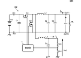
- FIG. 1 is a circuit diagram of a step-up DC-DC converter according to the first embodiment.
- the DC-DC converter 101 according to the first embodiment includes input terminals IN1 and IN2 to which a DC power supply Vin is connected, and output terminals OUT1 and OUT2 to which a load (main load of the present invention) RL is connected.
- the DC-DC converter 101 boosts the DC voltage input from the input terminals IN1 and IN2, and outputs the boosted DC voltage from the output terminals OUT1 and OUT2 to the load RL.
- the input capacitor C1 is connected to the input terminals IN1 and IN2.
- An inductor L1 and a switching element Q1 connected in series are connected to the input terminals IN1 and IN2.
- the switching element Q1 is an n-type MOS-FET, its drain is connected to the inductor L1, and its source is connected to the input terminal IN2.
- the switching element Q1 has a gate connected to a control unit (switching control circuit of the present invention) 10 described later, and is turned on and off when a control signal is input from the control unit 10.
- the diode D1 has an anode connected to the inductor L1 and a cathode connected to the output terminal OUT1. Smoothing capacitors C2 and C3 are connected to the cathode of the diode D1.
- the switching element Q1 described above corresponds to the switching circuit of the present invention, and the inductor L1 and the smoothing capacitors C2 and C3 correspond to the first smoothing circuit of the present invention.
- a connection point between the inductor L1 and the switching element Q1 includes a diode D2 and a smoothing capacitor C4.
- the diode D2 has an anode connected to the inductor L1 and a cathode connected to the smoothing capacitor C4.
- the smoothing circuit including the inductor L1 and the smoothing capacitor C4 corresponds to the second smoothing circuit of the present invention.
- the cathode of the diode D2 is provided with a voltage dividing circuit composed of resistors (subloads of the present invention) R1 and R2 of 10 k ⁇ , for example.
- the control unit 10 detects the output voltage of the second smoothing circuit using a voltage dividing circuit.
- the output voltage and Vo2 the output current is I 2.
- the control unit 10 outputs a control signal to the gate of the switching element Q1, controls the switching of the switching element Q1, and boosts the input DC voltage. Further, the control unit 10 detects the output voltage Vo2 and performs feedback control of the switching element Q1 so that the output voltage Vo2 is constant (reference voltage). As a result, the current-voltage characteristic in the DC-DC converter 101 has a gradient. Specifically, with an increase of the output current I 1, the output voltage Vo1 is reduced.
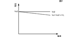
- FIG. 2 is a diagram showing current-voltage characteristics, and shows the characteristics of the output voltages Vo1 and Vo2 with respect to the output currents I 1 and I 2 .
- the control unit 10 so that the output voltage Vo2 regardless of the size of the output current I 2 is constant, the switching element Q1 is PWM controlled.
- the output current I 2 is determined by the resistors R1, R2, constant and does not vary substantially regardless of the load RL.
- a line connected to the diode D1 and a line connected to the diode D2 are connected in parallel to the connection point between the inductor L1 and the switching element Q1, and the diode D1 is connected when the load RL is unloaded. The resulting line becomes the output voltage Vo2. Since the output current I 2 is smaller than the output current I 1 (I 2 ⁇ I 1 ), the voltage drop of the line to which the diode D 2 is connected can be ignored.
- the output voltage Vo1 Vo2-r ⁇ output current I 1. Therefore, the output voltage Vo1 has a characteristic inclined from the voltage Vo2, as shown in FIG. The slope of the output voltage Vo1 is determined by the resistance r.
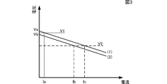
- FIG. 3 is a diagram showing current-voltage characteristics of two DC-DC converters driven in parallel. As shown in FIG. 3, the current-voltage characteristics of the two DC-DC converters are given a slope. As shown in characteristic (1) of FIG. 3, the first DC-DC converter has a current-voltage characteristic in which the output voltage decreases as the load increases, starting from the output voltage Va when no load is applied. As shown in the characteristic (2) of FIG. 3, the second DC-DC converter has a current-voltage characteristic in which the output voltage decreases as the load increases, starting from the output voltage Vb ( ⁇ Va) at no load. .
- the burden on the DC-DC converter 101 is reduced.
- a voltage drop resistor is not used in the current path to the load RL, so that loss occurs.
- the current-voltage characteristic can be given a gradient.
- power may be supplied to a small load such as a control IC by the output voltage Vo2 output from the second smoothing circuit (L1, C4). Even in this case, since the load change, such as the control IC is negligibly small, the output current I 2 to the secondary load can be said substantially constant.
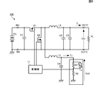
- FIG. 4 is a circuit diagram of the step-down DC-DC converter according to the second embodiment.
- the DC-DC converter 102 according to the second embodiment steps down the DC voltage input from the input terminals IN1 and IN2, and outputs the reduced DC voltage from the output terminals OUT1 and OUT2 to the load RL.
- a switching element Q1 and an inductor L2 connected in series are connected between the input terminal IN1 and the output terminal OUT1.
- the switching element Q1 is an n-type MOS-FET, its drain is connected to the input terminal IN1, and its source is connected to the inductor L2.
- the switching element Q2 is connected to the switching element Q1.
- the switching element Q2 is also an n-type MOS-FET, its drain is connected to the switching element Q1, and its source is connected to the input terminal IN2. Further, smoothing capacitors C2 and C3 are connected between the inductor L2 and the output terminal OUT1.
- the switching elements Q1 and Q2 are each turned on and off when a gate is connected to the control unit 11 and a control signal is input from the control unit 11.
- switching elements Q1 and Q2 are alternately turned on and off, whereby the DC voltage input from the input terminals IN1 and IN2 is stepped down, and the stepped-down DC voltage is output from the output terminals OUT1 and OUT2 to the load RL. Is done.
- Switching element Q2 may be a diode.
- the switching elements Q1 and Q2 described above correspond to the switching circuit of the present invention, and the inductor L2 and the smoothing capacitors C2 and C3 correspond to the first smoothing circuit of the present invention.
- a smoothing circuit (second smoothing circuit according to the present invention) including an inductor L3 and a smoothing capacitor C4 is connected to a connection point between the switching elements Q1 and Q2.
- a voltage dividing circuit including resistors R1 and R2 is connected to the smoothing circuit.
- the control unit 11 performs feedback control to make the output voltage Vo2 detected from the voltage dividing circuit constant, as in the control unit 10 of the first embodiment.
- the current-voltage characteristic of the DC-DC converter 102 can be given a slope without using a voltage drop resistor in the current path to the load RL and without generating a loss.
- the slope of the current-voltage characteristic is larger than that in the first embodiment.
- the third embodiment is an example in which the on-resistance of the switching element Q1 and the internal resistance of the inductor L2 of the DC-DC converter 102 according to the second embodiment are used for generating a current-voltage characteristic having a slope.
- FIG. 5 is a circuit diagram of a DC-DC converter according to the third embodiment.
- the switching element Q3 is connected to the input terminal IN1.
- the switching element Q3 is an n-type MOS-FET, the drain is connected to the input terminal IN1, and the source is connected to the inductor L3. Further, the switching element Q4 is connected to the switching element Q3.
- the switching elements Q1 and Q2 correspond to the first switching circuit according to the present invention
- the switching elements Q3 and Q4 correspond to the second switching circuit according to the present invention
- the inductor L2 and the smoothing capacitors C2 and C3 correspond to the first smoothing circuit according to the present invention
- the smoothing circuit including the inductor L3 and the smoothing capacitor C4 corresponds to the second smoothing circuit according to the present invention.
- the control unit 11 detects the output voltage Vo2 from the voltage dividing circuit including the resistors R1 and R2, and feedback-controls the switching elements Q1, Q2, Q3, and Q4 so that the output voltage Vo2 becomes constant (reference voltage).
- the current-voltage characteristic can be given a slope.
- the slope of the current-voltage characteristic is determined by the ON resistance of the switching element Q1, the internal resistance of the inductor L2, and the wiring resistance. Therefore, the slope of the voltage-current characteristic of the third embodiment is larger by the on-resistance of the switching element Q1 than that of the second embodiment.
- the voltage-current characteristic can be inclined without using a voltage drop resistor in the current path to the load RL. Furthermore, by using the on-resistance of the switching element Q1, it is possible to realize voltage-current characteristics having a larger slope than those of the first and second embodiments.
- the fourth embodiment shows an example of an interleaved DC-DC converter configured by arranging two DC-DC converters 102 according to the second embodiment in parallel.
- FIG. 6 is a circuit diagram of a DC-DC converter according to the fourth embodiment.
- the switching element Q5 and the inductor L4 are connected to the input terminal IN1.
- the inductor L4 is connected to the output terminal OUT1.
- a smoothing circuit composed of an inductor L5 and a smoothing capacitor C4 is connected to the switching element Q5.
- the switching elements Q1 and Q2 correspond to the first switching circuit according to the present invention
- the switching elements Q5 and Q6 correspond to the second switching circuit according to the present invention
- the inductors L2, L3 and the smoothing capacitors C2, C3, C4 correspond to the third smoothing circuit according to the present invention
- the inductors L4, L5 and the smoothing capacitors C2, C3, C4 are the fourth smoothing circuit according to the present invention. It corresponds to.
- Switching elements Q1 and Q2 are switching controlled by drive circuit 13A, and switching elements Q5 and Q6 are switching controlled by drive circuit 13B.
- the drive circuits 13A and 13B receive a drive signal from the control unit 12.
- the drive circuit 13A and the drive circuit 13B perform switching control of the switching element Q1 and the switching element Q5 with a phase difference of 180 degrees from each other, and the switching element Q2 and the switching element Q6 respectively 180 degrees. Switching control is performed with a phase difference of degree.
- the control unit 12 performs feedback control to keep the output voltage Vo2 detected from the voltage dividing circuit constant. As a result, the current-voltage characteristic can be inclined without using a voltage drop resistor in the current path to the load RL. Further, by making the interleaving scheme, it is possible to reduce the ripple of the output current I 1.
- the fifth embodiment is an example in which a protection circuit is provided in the case where a disconnection occurs in a circuit for controlling the output voltage Vo2, such as damage to the inductor L3 and the resistor R4 in the DC-DC converter 102 of the second embodiment.
- FIG. 7 is a circuit diagram of a DC-DC converter according to the fifth embodiment.
- a resistor R4 is connected between the inductor L3 and the resistors R1 and R2.
- the connection point between the resistors R4 and R1 is connected to the output terminal OUT1 through the resistor R3.
- the control unit 10 detects the output voltage Vo2 from the voltage dividing circuit (resistors R4, R1, R2).
- the current that flows when the switching element Q1 is turned on does not flow through the line passing through the inductor L3.
- the current passing through the inductor L2 flows to the resistors R1 and R2 via the resistor R3.
- the control unit 10 detects the output voltage Vo1 from the voltage dividing circuit (resistors R3, R1, R2).
- the sixth embodiment shows an example in which the voltage dividing circuit of the DC-DC converter according to the second embodiment is a temperature-dependent resistance voltage dividing circuit.
- FIG. 8 is a circuit diagram of a DC-DC converter according to the sixth embodiment.
- the DC-DC converter 106 includes a thermistor Th connected in parallel to the resistor R1.
- the resistance value of the thermistor Th is determined according to the temperatures of the switching elements Q1, Q2 and the inductor L2. The resistance value changes with temperature, and as a result, the output voltage Vo2 detected by the control unit 10 also changes. Since the output voltage Vo2 varies with temperature, load distribution of the DC-DC converter 106 can be realized.
- FIG. 9 is a diagram showing current-voltage characteristics with temperature changes. For example, when two DC-DC converters are driven in parallel, when the load applied to the first DC-DC converter is large and the heat generation is larger than that of the second DC-DC converter, as shown in FIG. The current-voltage characteristic of the first DC-DC converter shifts to a lower one than the characteristic at normal temperature. As a result, the output current of the first DC-DC converter decreases and the temperature decreases.
- the current-voltage characteristic of the first DC-DC converter is as shown in FIG. Shift to higher than normal temperature characteristics.
- the output current of the first DC-DC converter increases and the temperature rises.
- the load applied to the first DC-DC converter increases, the load applied to the second DC-DC converter decreases.
- the output current from the second DC-DC converter decreases, and the temperature of the second DC-DC converter drops.
- the seventh embodiment is an example including a circuit for controlling a transient response generated in the DC-DC converter 102 according to the second embodiment.
- FIG. 10 is a circuit diagram of the DC-DC converter according to the seventh embodiment.
- a DC-DC converter 107 shown in FIG. 10 includes a CR series circuit including a resistor R5 and a capacitor C5 in addition to the configuration of the DC-DC converter 102 according to the second embodiment. This CR series circuit is connected between the connection point of the resistors R1 and R2 and the output terminal OUT1.
- the control unit 10 of the DC-DC converter 107 detects the output voltage from the CR series circuit and performs feedback control.
- the output current I 1 it is possible to enhance the response in the case of increasing or decreasing rapidly.
- the CR series circuit for controlling the transient response is applied to the step-down DC-DC converter.
- the CR series circuit is different from the step-up DC-DC converter. Can be applied similarly.
Landscapes
- Engineering & Computer Science (AREA)
- Power Engineering (AREA)
- Dc-Dc Converters (AREA)
Abstract
DC-DCコンバータ(101)は、スイッチング素子(Q1)によりスイッチングされる電圧電流を平滑する平滑回路と、スイッチング素子(Q1)の制御により平滑回路の出力電圧電流を制御する制御部(10)とを備える。平滑回路は、インダクタ(L1)及び平滑コンデンサ(C2,C3)からなる第1平滑回路と、インダクタ(L1)及びキャパシタ(C4)からなる第2平滑回路とを備える。第1平滑回路は、スイッチング素子(Q1)によりスイッチングされる電圧電流を平滑して負荷(RL)へ供給する。第2平滑回路は、スイッチング素子(Q1)によりスイッチングされる電圧電流を平滑して分圧回路(R1,R2)へ供給する。制御部(10)は、分圧回路へ供給される電圧が一定となるようスイッチング素子(Q1)をフィードバック制御する。これにより、損失が生じることなく、出力電圧特性に傾きを持たせることができるDC-DCコンバータを提供する。
Description
本発明は、電流電圧特性に所定の勾配を持たせたDC-DCコンバータに関する。
高出力化のために、複数の電源を並列に接続して構成される電源装置がある。複数の電源を用いる場合、それぞれの電源にかかる負荷を分散して、電源の負担を均等にすることを目的とする様々な方式が提案されている。例えば、特許文献1には、複数の電圧源を並列接続して構成される並列駆動型電源装置が開示されている。
特許文献1に記載の並列駆動型電源装置は、二つのDC-DCコンバータを備えている。特許文献1では、各DC-DCコンバータの出力側に抵抗を挿入して、DC-DCコンバータそれぞれの電流電圧特性(電流変化に対する電圧変化を示す特性)に傾きを与え、さらに、その傾きが同じになるようにしている。この構成において、並列駆動型電源装置に接続される負荷への出力電流が小さいと、出力電圧が高い方のDC-DCコンバータのみが電流を出力し、負荷への出力電流が大きくなると、両方のDC-DCコンバータが電流を出力する。このように、二つのDC-DCコンバータそれぞれにかかる負荷を分散している。
しかしながら、特許文献1では、DC-DCコンバータの負荷電流の経路に抵抗を接続しているため、抵抗による損失が発生し、変換効率が低下するといった問題がある。
そこで、本発明の目的は、損失が生じることなく、電流電圧特性に傾きを持たせることができるDC-DCコンバータを提供することにある。
本発明は、直流電源入力部に入力される電圧電流をスイッチングするスイッチング回路、前記スイッチング回路によりスイッチングされる電圧電流を平滑する平滑回路と、前記スイッチング回路の制御により前記平滑回路の出力電圧電流を制御するスイッチング制御回路と、を備えるDC-DCコンバータにおいて、前記平滑回路は、前記スイッチング回路によりスイッチングされる電圧電流を平滑して主負荷へ供給する第1平滑回路と、前記スイッチング回路によりスイッチングされる電圧電流を平滑して副負荷へ供給する第2平滑回路と、を備え、前記スイッチング制御回路は、前記副負荷へ供給される電圧と基準電圧との比較に応じて前記スイッチング回路をフィードバック制御することを特徴とする。
本発明は、直流電源入力部に入力される電圧電流をスイッチングするスイッチング回路、前記スイッチング回路によりスイッチングされる電圧電流を平滑する平滑回路と、前記スイッチング回路の制御により前記平滑回路の出力電圧電流を制御するスイッチング制御回路と、を備えるDC-DCコンバータにおいて、前記スイッチング回路は、前記直流電源入力部に入力される電圧電流をそれぞれスイッチングする第1のスイッチング回路および第2のスイッチング回路を備え、前記平滑回路は、前記第1のスイッチング回路によりスイッチングされる電圧電流を平滑して主負荷へ供給する第1平滑回路と、前記第2のスイッチング回路によりスイッチングされる電圧電流を平滑して副負荷へ供給する第2平滑回路と、を備え、前記スイッチング制御回路は、前記副負荷へ供給される電圧と基準電圧との比較に応じて前記第1のスイッチング回路および前記第2のスイッチング回路をフィードバック制御することを特徴とする。
本発明は、直流電源入力部に入力される電圧電流をスイッチングするスイッチング回路、前記スイッチング回路によりスイッチングされる電圧電流を平滑する平滑回路と、前記スイッチング回路の制御により前記平滑回路の出力電圧電流を制御するスイッチング制御回路と、を備えるDC-DCコンバータにおいて、前記スイッチング回路は、前記直流電源入力部に入力される電圧電流をそれぞれスイッチングする第3のスイッチング回路および第4のスイッチング回路、を備え、前記平滑回路は、前記第3のスイッチング回路によりスイッチングされる電圧電流を平滑して主負荷および副負荷へ供給する第3平滑回路と、前記第4のスイッチング回路によりスイッチングされる電圧電流を平滑して主負荷および副負荷へ供給する第4平滑回路と、を備え、前記スイッチング制御回路は、前記副負荷へ供給される電圧と基準電圧との比較に応じて前記第3のスイッチング回路および前記第4のスイッチング回路をフィードバック制御することを特徴とする。
これらの構成では、主負荷への出力電圧ではなく、副負荷への出力電圧によってスイッチング回路をスイッチング制御する。これにより、主負荷への出力電流に関係なく(負荷一定の状態で)、スイッチング回路からの出力電圧が一定となるようにスイッチング制御される。スイッチング回路からの出力電圧が一定の場合、素子の内部抵抗および配線抵抗(以下、総抵抗という)などの影響により、主負荷への出力電圧はスイッチング回路からの出力電圧よりも、「総抵抗×主負荷への電流」の分だけ低下する。したがって、主負荷への出力電流の増加に伴い、出力電圧は低下する。この結果、電圧降下用の抵抗を用いることなく、すなわち、その抵抗による損失が生じることなく、電流電圧特性に傾きを持たせることができる。
前記副負荷は、印加電圧に対する出力電圧に温度依存性のある抵抗分圧回路を備えた構成でもよい。
この構成では、温度により電圧勾配をシフトすることができ、並列動作時に特定のDC-DCコンバータに電流が集中する(発熱が集中する)ことを防ぐことができる。その結果、バランスのよい並列動作が実現できる。
本発明によれば、電圧降下用の抵抗を用いることなく、電流電圧特性に傾きを持たせることができる。
(実施形態1)
実施形態1では、本発明に係るDC-DCコンバータを、入力された直流電圧を昇圧する昇圧型DC-DCコンバータとし、そのDC-DCコンバータのドループ特性を生成する例について説明する。
実施形態1では、本発明に係るDC-DCコンバータを、入力された直流電圧を昇圧する昇圧型DC-DCコンバータとし、そのDC-DCコンバータのドループ特性を生成する例について説明する。
図1は実施形態1に係る昇圧型DC-DCコンバータの回路図である。実施形態1に係るDC-DCコンバータ101は、直流電源Vinが接続された入力端子IN1,IN2と、負荷(本発明の主負荷)RLが接続された出力端子OUT1,OUT2とを備えている。DC-DCコンバータ101は、入力端子IN1,IN2から入力される直流電圧を昇圧し、昇圧した直流電圧を出力端子OUT1,OUT2から負荷RLへ出力する。
以下では、出力端子OUT1,OUT2からの出力電流をI1とし、出力電圧をVo1とする。
入力端子IN1,IN2には入力コンデンサC1が接続されている。入力端子IN1,IN2には、直列接続されたインダクタL1およびスイッチング素子Q1が接続されている。スイッチング素子Q1はn型MOS-FETであり、そのドレインがインダクタL1に接続され、ソースが入力端子IN2に接続されている。また、スイッチング素子Q1は、そのゲートが後述の制御部(本発明のスイッチング制御回路)10に接続され、制御部10から制御信号が入力されることでオンオフする。
入力端子IN1と出力端子OUT1との間には、上述のインダクタL1と、そのインダクタL1に直列接続されたダイオードD1とが接続されている。ダイオードD1は、そのアノードがインダクタL1に接続され、カソードが出力端子OUT1に接続されている。ダイオードD1のカソードには、平滑コンデンサC2,C3が接続されている。
この構成において、スイッチング素子Q1がオンオフされることで、入力端子IN1,IN2から入力された直流電圧が昇圧され、昇圧された直流電圧が出力端子OUT1,OUT2から負荷RLへ出力される。
なお、上述のスイッチング素子Q1は、本発明のスイッチング回路に相当し、インダクタL1および平滑コンデンサC2,C3は、本発明の第1平滑回路に相当する。
インダクタL1およびスイッチング素子Q1の接続点には、ダイオードD2および平滑コンデンサC4を備えている。ダイオードD2は、そのアノードがインダクタL1に接続され、カソードが平滑コンデンサC4に接続されている。なお、上述のインダクタL1および平滑コンデンサC4からなる平滑回路は、本発明の第2平滑回路に相当する。
ダイオードD2のカソードには、例えば10kΩの抵抗(本発明の副負荷)R1,R2からなる分圧回路を備えている。制御部10は、分圧回路により第2平滑回路の出力電圧を検出する。以下では、この出力電圧をVo2とし、出力電流をI2とする。
制御部10は、スイッチング素子Q1のゲートへ制御信号を出力し、スイッチング素子Q1をスイッチング制御して、入力された直流電圧を昇圧する。また、制御部10は、出力電圧Vo2を検出し、出力電圧Vo2が一定(基準電圧)となるようスイッチング素子Q1をフィードバック制御する。これにより、DC-DCコンバータ101における電流電圧特性は勾配を有するようになる。具体的には、出力電流I1の増加に伴い、出力電圧Vo1は低下する。
図2は、電流電圧特性を示す図であり、出力電流I1,I2に対する出力電圧Vo1,Vo2の特性を示す。図2に示すように、制御部10は出力電流I2の大きさに関係なく出力電圧Vo2が一定となるよう、スイッチング素子Q1をPWM制御する。ただし、出力電流I2は抵抗R1,R2により決まるため、負荷RLに依らず一定であり実質的に変動しない。インダクタL1とスイッチング素子Q1との接続点には、ダイオードD1が接続されたラインと、ダイオードD2が接続されたラインとが並列接続されており、負荷RLが無負荷の場合にはダイオードD1が接続されたラインは出力電圧Vo2となる。なお、出力電流I2は、出力電流I1よりも小さいため(I2≪I1)、ダイオードD2が接続されたラインの電圧降下分は無視できる。
ダイオードD1が接続されたラインにはダイオードD1の内部抵抗および配線抵抗など(これら総抵抗をrとする)が存在する。そのため、インダクタL1と出力端子OUT1との間では、「r×出力電流I1」の電圧降下が発生する。その結果、出力電圧Vo1=Vo2-r×出力電流I1となる。したがって、出力電圧Vo1は、図2に示すように、電圧Vo2から傾斜した特性となる。なお、出力電圧Vo1の傾きは抵抗rによって定まる。
電流電圧特性に傾きを持たせることで、例えば、二つのDC-DCコンバータを並列駆動した場合、二つのDC-DCコンバータそれぞれにかかる負荷を分散することができる。図3は、並列駆動する二つのDC-DCコンバータの電流電圧特性を示す図である。図3に示すように、二つのDC-DCコンバータの電流電圧特性に傾きを持たせる。第1のDC-DCコンバータは、図3の特性(1)に示すように、無負荷時の出力電圧Vaを始点として、負荷の増加と共に出力電圧が減少する電流電圧特性を有する。第2のDC-DCコンバータは、図3の特性(2)に示すように、無負荷時の出力電圧Vb(<Va)を始点として、負荷の増加と共に出力電圧が減少する電流電圧特性を有する。
この二つのDC-DCコンバータを並列駆動させる場合、負荷への出力電流が小さいときには(出力電流Iaのとき)、第1のDC-DCコンバータのみが電圧V1を出力する。すなわち、負荷は第1のDC-DCコンバータのみにかかる。負荷への出力電流が大きくなると(出力電流Ibのとき)、第1のDC-DCコンバータと第2のDC-DCコンバータとはそれぞれ電圧V2を出力する。このとき、第1のDC-DCコンバータは出力電流Icを出力し、第2のDC-DCコンバータは出力電流Ibを出力する。すなわち、第1および第2のDC-DCコンバータの双方に負荷がかかり、出力電流Ib+Icを出力する。
このように、図1に示すDC-DCコンバータ101の電流電圧特性が、図2に示すような勾配を有することで、負荷RLへの出力電流I1が増大することにより、出力電圧Vo1は低下し、DC-DCコンバータ101の負担は軽減される。そして、本実施形態では、分圧回路から検出した出力電圧Vo2を一定にするフィードバック制御を行うことで、負荷RLへの電流経路に電圧降下用の抵抗を用いることがないため、損失を生じさせることなく、電流電圧特性に勾配を持たせることができる。ここで、第2平滑回路(L1,C4)から出力される出力電圧Vo2によって、例えば制御ICなどの小負荷に電力が供給されてもよい。この場合であっても、制御ICなどの負荷変動は小さく無視できるので、副負荷への出力電流I2は実質的に一定といえる。
(実施形態2)
実施形態2では、本発明に係るDC-DCコンバータを、入力された直流電圧を降圧する降圧型DC-DCコンバータとし、電流電圧特性に傾きを持たせる例について説明する。以下、実施形態1と同様の部品については同じ符号を付し、説明は省略する。
実施形態2では、本発明に係るDC-DCコンバータを、入力された直流電圧を降圧する降圧型DC-DCコンバータとし、電流電圧特性に傾きを持たせる例について説明する。以下、実施形態1と同様の部品については同じ符号を付し、説明は省略する。
図4は実施形態2に係る降圧型DC-DCコンバータの回路図である。実施形態2に係るDC-DCコンバータ102は、入力端子IN1,IN2から入力された直流電圧を降圧し、降圧した直流電圧を出力端子OUT1,OUT2から負荷RLへ出力する。
入力端子IN1と出力端子OUT1との間には、直列接続されたスイッチング素子Q1およびインダクタL2が接続されている。スイッチング素子Q1はn型MOS-FETであり、そのドレインが入力端子IN1に接続され、ソースがインダクタL2に接続されている。
スイッチング素子Q1には、スイッチング素子Q2が接続されている。スイッチング素子Q2もn型MOS-FETであり、そのドレインがスイッチング素子Q1に接続され、ソースが入力端子IN2に接続されている。また、インダクタL2と出力端子OUT1との間には、平滑コンデンサC2,C3が接続されている。
スイッチング素子Q1,Q2はそれぞれ、ゲートが制御部11に接続され、制御部11から制御信号が入力されることでオンオフする。
この構成において、スイッチング素子Q1,Q2が交互にオンオフされることで、入力端子IN1,IN2から入力された直流電圧が降圧され、降圧された直流電圧が出力端子OUT1,OUT2から負荷RLへと出力される。なお、スイッチング素子Q2はダイオードであってもよい。
上述のスイッチング素子Q1,Q2は、本発明のスイッチング回路に相当し、インダクタL2および平滑コンデンサC2,C3は、本発明の第1平滑回路に相当する。
スイッチング素子Q1,Q2の接続点には、インダクタL3および平滑コンデンサC4からなる平滑回路(本発明に係る第2平滑回路)が接続されている。この平滑回路には、実施形態1と同様に、抵抗R1,R2からなる分圧回路が接続されている。
制御部11は、実施形態1の制御部10と同様に、分圧回路から検出した出力電圧Vo2を一定にするフィードバック制御を行う。これにより、負荷RLへの電流経路に電圧降下用の抵抗を用いずに、損失を発生させることなく、DC-DCコンバータ102の電流電圧特性に傾きを持たせることができる。この実施形態2では、負荷RLへの電流経路にインダクタL2の内部抵抗が存在するため、電流電圧特性の傾きは、実施形態1よりも大きくなる。
(実施形態3)
実施形態3は、実施形態2に係るDC-DCコンバータ102のスイッチング素子Q1のオン抵抗およびインダクタL2の内部抵抗を、傾きを持つ電流電圧特性の生成に用いる例である。図5は、実施形態3に係るDC-DCコンバータの回路図である。
実施形態3は、実施形態2に係るDC-DCコンバータ102のスイッチング素子Q1のオン抵抗およびインダクタL2の内部抵抗を、傾きを持つ電流電圧特性の生成に用いる例である。図5は、実施形態3に係るDC-DCコンバータの回路図である。
入力端子IN1にはスイッチング素子Q3が接続されている。スイッチング素子Q3はn型MOS-FETであり、ドレインが入力端子IN1に接続され、ソースがインダクタL3に接続されている。また、スイッチング素子Q3には、スイッチング素子Q4が接続されている。
なお、DC-DCコンバータ103において、スイッチング素子Q1,Q2は、本発明に係る第1のスイッチング回路に相当し、スイッチング素子Q3,Q4は、本発明に係る第2のスイッチング回路に相当する。また、インダクタL2および平滑コンデンサC2,C3は、本発明に係る第1平滑回路に相当し、インダクタL3および平滑コンデンサC4からなる平滑回路は、本発明に係る第2平滑回路に相当する。
制御部11は、抵抗R1,R2からなる分圧回路から出力電圧Vo2を検出し、出力電圧Vo2が一定(基準電圧)となるようスイッチング素子Q1,Q2,Q3,Q4をフィードバック制御する。これにより、実施形態2と同様に、電流電圧特性に傾きを持たせることができる。このDC-DCコンバータ103の回路では、電流電圧特性の傾きは、スイッチング素子Q1のオン抵抗、インダクタL2の内部抵抗および配線抵抗によって定まる。したがって、実施形態3の電圧電流特性の傾きは、実施形態2と比べて、スイッチング素子Q1のオン抵抗分だけ大きい。
このように、実施形態3は、実施形態1,2と同様に、負荷RLへの電流経路に電圧降下用の抵抗を用いることなく、電圧電流特性に傾きを持たせることができる。さらに、スイッチング素子Q1のオン抵抗を利用することで、実施形態1,2よりも大きな傾きを持つ電圧電流特性を実現できる。
(実施形態4)
実施形態4は、実施形態2に係るDC-DCコンバータ102を二つ並列に配置して構成したインターリーブ方式のDC-DCコンバータを例に示す。図6は、実施形態4に係るDC-DCコンバータの回路図である。
実施形態4は、実施形態2に係るDC-DCコンバータ102を二つ並列に配置して構成したインターリーブ方式のDC-DCコンバータを例に示す。図6は、実施形態4に係るDC-DCコンバータの回路図である。
入力端子IN1には、スイッチング素子Q5およびインダクタL4が接続されている。インダクタL4は出力端子OUT1に接続されている。また、スイッチング素子Q5には、インダクタL5および平滑コンデンサC4からなる平滑回路が接続されている。
DC-DCコンバータ104において、スイッチング素子Q1,Q2は、本発明に係る第1のスイッチング回路に相当し、スイッチング素子Q5,Q6は、本発明に係る第2のスイッチング回路に相当する。また、インダクタL2,L3および平滑コンデンサC2,C3,C4は、本発明に係る第3平滑回路に相当し、インダクタL4,L5および平滑コンデンサC2,C3,C4は、本発明に係る第4平滑回路に相当する。
スイッチング素子Q1,Q2はドライブ回路13Aによりスイッチング制御され、スイッチング素子Q5,Q6はドライブ回路13Bによりスイッチング制御される。また、ドライブ回路13A,13Bは、制御部12から駆動信号が入力される。そして、ドライブ回路13Aとドライブ回路13Bとは、スイッチング素子Q1とスイッチング素子Q5とを、それぞれ互いに180度の位相差をもたせてスイッチング制御し、またスイッチング素子Q2とスイッチング素子Q6とを、それぞれ互いに180度の位相差をもたせてスイッチング制御する。
制御部12は、分圧回路から検出した出力電圧Vo2を一定にするフィードバック制御を行う。これにより、負荷RLへの電流経路に電圧降下用の抵抗を用いることなく、電流電圧特性に傾きを持たせることができる。また、インターリーブ方式とすることで、出力電流I1のリップルを軽減することができる。
(実施形態5)
実施形態5は、実施形態2のDC-DCコンバータ102におけるインダクタL3や抵抗R4が破損するなど、出力電圧Vo2を制御するための回路に断線が発生した場合の保護回路を設けた例である。
実施形態5は、実施形態2のDC-DCコンバータ102におけるインダクタL3や抵抗R4が破損するなど、出力電圧Vo2を制御するための回路に断線が発生した場合の保護回路を設けた例である。
図7は、実施形態5に係るDC-DCコンバータの回路図である。図7に示すDC-DCコンバータ105では、インダクタL3と抵抗R1,R2との間に抵抗R4が接続されている。また、抵抗R4,R1の接続点は、抵抗R3を介して出力端子OUT1に接続されている。各抵抗値は、例えば、抵抗R1,R2=10kΩ、抵抗R3=1kΩ、抵抗R4=10Ωである。
この回路構成において、正常時では、スイッチング素子Q1のオン時に流れる電流は、インダクタL3を通り、抵抗R4,R1,R2へ流れる。そして、制御部10は、分圧回路(抵抗R4,R1,R2)から出力電圧Vo2を検出する。一方、インダクタL3の破損などにより断線が生じた場合、スイッチング素子Q1のオン時に流れる電流は、インダクタL3を通るラインには電流が流れない。この場合、インダクタL2を通る電流が、抵抗R3を介して、抵抗R1,R2に流れる。これにより、制御部10は、分圧回路(抵抗R3,R1,R2)から出力電圧Vo1を検出することになる。
このように、実施形態5に係るDC-DCコンバータ105では、断線などの異常が生じた場合であっても、過電圧を出力するという異常を防止できる。
(実施形態6)
実施形態6は、実施形態2に係るDC-DCコンバータの分圧回路を温度依存性のある抵抗分圧回路とした例を示す。
実施形態6は、実施形態2に係るDC-DCコンバータの分圧回路を温度依存性のある抵抗分圧回路とした例を示す。
図8は、実施形態6に係るDC-DCコンバータの回路図である。DC-DCコンバータ106は、実施形態2で説明したDC-DCコンバータ102の回路構成に加え、抵抗R1に並列接続されたサーミスタThを備えた構成である。サーミスタThはスイッチング素子Q1,Q2およびインダクタL2などの温度に応じて抵抗値が定まる。抵抗値が温度によって変化し、その結果、制御部10が検出する出力電圧Vo2も変化する。出力電圧Vo2が温度によって変化するため、DC-DCコンバータ106の負荷分散が実現できる。
図9は温度変化に伴う電流電圧特性を示す図である。例えば、二つのDC-DCコンバータを並列駆動させる場合において、第1のDC-DCコンバータにかかる負荷が大きく、第2のDC-DCコンバータに比べて発熱が大きいとき、図9に示すように、第1のDC-DCコンバータの電流電圧特性が、常温時の特性より低い方にシフトする。この結果、第1のDC-DCコンバータの出力電流は低下し、温度は降下する。
また、第1のDC-DCコンバータの出力電流が低下することで、第2のDC-DCコンバータへ負荷が分散され、第2のDC-DCコンバータからの出力電流が増加する。その結果、第2のDC-DCコンバータの発熱が大きくなる。これにより、二つのDC-DCコンバータの発熱のバランスが保たれる。
一方、第1のDC-DCコンバータにかかる負荷が小さく、第2のDC-DCコンバータに比べて発熱が小さいとき、図9に示すように、第1のDC-DCコンバータの電流電圧特性は、常温時の特性より高い方にシフトする。この結果、第1のDC-DCコンバータの出力電流は増加し、温度は上昇する。第1のDC-DCコンバータの出力電流が増加する、すなわち、第1のDC-DCコンバータにかかる負荷が大きくなることで、第2のDC-DCコンバータにかかる負荷は小さくなる。その結果、第2のDC-DCコンバータからの出力電流が減少し、第2のDC-DCコンバータの温度は降下する。これにより、二つのDC-DCコンバータの発熱のバランスが保たれる。
以上のように、温度に応じて電流電圧特性をシフトさせることで、並列駆動時に一つのDC-DCコンバータへの熱集中を防止できる。
(実施形態7)
実施形態7は、実施形態2に係るDC-DCコンバータ102に生じる過渡応答を制御する回路を備えた例である。
実施形態7は、実施形態2に係るDC-DCコンバータ102に生じる過渡応答を制御する回路を備えた例である。
図10は、実施形態7に係るDC-DCコンバータの回路図である。図10に示すDC-DCコンバータ107は、実施形態2に係るDC-DCコンバータ102の構成に加え、抵抗R5およびキャパシタC5からなるCR直列回路を備えている。このCR直列回路は、抵抗R1,R2の接続点と出力端子OUT1との間に接続されている。
DC-DCコンバータ107の制御部10は、過渡応答の場合には、CR直列回路からの出力電圧を検出して、フィードバック制御する。これにより、出力電流I1が急激に増加または減少した場合の応答性を高めることができる。
なお、実施形態7では、過渡応答の制御のためのCR直列回路を降圧型DC-DCコンバータに適用させた場合の例を示したが、CR直列回路は、昇圧型DC-DCコンバータに対しても同様に適用できる。
10,11,12-制御部
13A,13B-ドライブ回路
101,102,103,104,105,106-DC-DCコンバータ
C1-入力コンデンサ
C2,C3,C4-平滑コンデンサ
D1,D2-ダイオード
L1,L2,L3,L4,L5-インダクタ
Q1,Q2,Q3,Q4,Q5,Q6-スイッチング素子
RL-負荷
R1,R2-分圧抵抗
R3,R4-抵抗
Vi-直流電源
IN1,IN2-入力端子(直流電源入力部)
OUT1,OUT2-出力端子
13A,13B-ドライブ回路
101,102,103,104,105,106-DC-DCコンバータ
C1-入力コンデンサ
C2,C3,C4-平滑コンデンサ
D1,D2-ダイオード
L1,L2,L3,L4,L5-インダクタ
Q1,Q2,Q3,Q4,Q5,Q6-スイッチング素子
RL-負荷
R1,R2-分圧抵抗
R3,R4-抵抗
Vi-直流電源
IN1,IN2-入力端子(直流電源入力部)
OUT1,OUT2-出力端子
Claims (4)
- 直流電源入力部に入力される電圧電流をスイッチングするスイッチング回路、前記スイッチング回路によりスイッチングされる電圧電流を平滑する平滑回路と、前記スイッチング回路の制御により前記平滑回路の出力電圧電流を制御するスイッチング制御回路と、を備えるDC-DCコンバータにおいて、
前記平滑回路は、
前記スイッチング回路によりスイッチングされる電圧電流を平滑して主負荷へ供給する第1平滑回路と、
前記スイッチング回路によりスイッチングされる電圧電流を平滑して副負荷へ供給する第2平滑回路と、
を備え、
前記スイッチング制御回路は、
前記副負荷へ供給される電圧と基準電圧との比較に応じて前記スイッチング回路をフィードバック制御する、
DC-DCコンバータ。 - 直流電源入力部に入力される電圧電流をスイッチングするスイッチング回路、前記スイッチング回路によりスイッチングされる電圧電流を平滑する平滑回路と、前記スイッチング回路の制御により前記平滑回路の出力電圧電流を制御するスイッチング制御回路と、を備えるDC-DCコンバータにおいて、
前記スイッチング回路は、
前記直流電源入力部に入力される電圧電流をそれぞれスイッチングする第1のスイッチング回路および第2のスイッチング回路を備え、
前記平滑回路は、
前記第1のスイッチング回路によりスイッチングされる電圧電流を平滑して主負荷へ供給する第1平滑回路と、
前記第2のスイッチング回路によりスイッチングされる電圧電流を平滑して副負荷へ供給する第2平滑回路と、
を備え、
前記スイッチング制御回路は、
前記副負荷へ供給される電圧と基準電圧との比較に応じて前記第1のスイッチング回路および前記第2のスイッチング回路をフィードバック制御する、
DC-DCコンバータ。 - 直流電源入力部に入力される電圧電流をスイッチングするスイッチング回路、前記スイッチング回路によりスイッチングされる電圧電流を平滑する平滑回路と、前記スイッチング回路の制御により前記平滑回路の出力電圧電流を制御するスイッチング制御回路と、を備えるDC-DCコンバータにおいて、
前記スイッチング回路は、
前記直流電源入力部に入力される電圧電流をそれぞれスイッチングする第1のスイッチング回路および第2のスイッチング回路、
を備え、
前記平滑回路は、
前記第1のスイッチング回路によりスイッチングされる電圧電流を平滑して主負荷および副負荷へ供給する第3平滑回路と、
前記第2のスイッチング回路によりスイッチングされる電圧電流を平滑して主負荷および副負荷へ供給する第4平滑回路と、
を備え、
前記スイッチング制御回路は、
前記副負荷へ供給される電圧と基準電圧との比較に応じて前記第1のスイッチング回路および前記第2のスイッチング回路をフィードバック制御する、
DC-DCコンバータ。 - 前記副負荷は、印加電圧に対する出力電圧に温度依存性のある抵抗分圧回路を備えた、請求項1から3の何れかに記載のDC-DCコンバータ。
Priority Applications (3)
| Application Number | Priority Date | Filing Date | Title |
|---|---|---|---|
| CN201480006137.6A CN104956575B (zh) | 2013-02-08 | 2014-02-06 | 电源装置 |
| EP14748545.2A EP2955830A4 (en) | 2013-02-08 | 2014-02-06 | CONTINUOUS-CONTINUOUS CONVERTER |
| JP2014560793A JP5979252B2 (ja) | 2013-02-08 | 2014-02-06 | 電源装置 |
Applications Claiming Priority (2)
| Application Number | Priority Date | Filing Date | Title |
|---|---|---|---|
| JP2013022978 | 2013-02-08 | ||
| JP2013-022978 | 2013-02-08 |
Publications (1)
| Publication Number | Publication Date |
|---|---|
| WO2014123173A1 true WO2014123173A1 (ja) | 2014-08-14 |
Family
ID=51299765
Family Applications (1)
| Application Number | Title | Priority Date | Filing Date |
|---|---|---|---|
| PCT/JP2014/052715 Ceased WO2014123173A1 (ja) | 2013-02-08 | 2014-02-06 | Dc-dcコンバータ |
Country Status (4)
| Country | Link |
|---|---|
| EP (1) | EP2955830A4 (ja) |
| JP (1) | JP5979252B2 (ja) |
| CN (1) | CN104956575B (ja) |
| WO (1) | WO2014123173A1 (ja) |
Cited By (3)
| Publication number | Priority date | Publication date | Assignee | Title |
|---|---|---|---|---|
| WO2016088189A1 (ja) * | 2014-12-02 | 2016-06-09 | 富士電機株式会社 | 直流電源装置の制御方法及び制御装置 |
| CN113890356A (zh) * | 2021-09-10 | 2022-01-04 | 三峡大学 | 一种新型的高增益双输入dc-dc变换器 |
| JP7511713B1 (ja) | 2023-05-24 | 2024-07-05 | 昭憲 春木 | トランジスタ回路及び電力変換回路 |
Families Citing this family (1)
| Publication number | Priority date | Publication date | Assignee | Title |
|---|---|---|---|---|
| JP6545310B1 (ja) * | 2018-03-22 | 2019-07-17 | 三菱電機株式会社 | 電力変換装置 |
Citations (6)
| Publication number | Priority date | Publication date | Assignee | Title |
|---|---|---|---|---|
| JP2002010642A (ja) * | 2000-06-21 | 2002-01-11 | Canon Inc | 電源装置およびその出力制御方法 |
| JP2005168090A (ja) | 2003-11-28 | 2005-06-23 | Tdk Corp | 並列駆動型電源装置 |
| JP2010088152A (ja) * | 2008-09-29 | 2010-04-15 | Toyota Motor Corp | スイッチング電源装置 |
| WO2011040325A1 (ja) * | 2009-09-30 | 2011-04-07 | 東芝ライテック株式会社 | 直流電源給電システム |
| JP2011176986A (ja) * | 2010-02-25 | 2011-09-08 | Dx Antenna Co Ltd | 寿命検出回路 |
| JP2012105481A (ja) * | 2010-11-11 | 2012-05-31 | Denso Corp | 電圧調整装置 |
Family Cites Families (4)
| Publication number | Priority date | Publication date | Assignee | Title |
|---|---|---|---|---|
| JP3427935B1 (ja) * | 2002-10-11 | 2003-07-22 | ローム株式会社 | スイッチング電源装置 |
| US6853562B2 (en) * | 2003-06-26 | 2005-02-08 | Optimum Power Conversion, Inc. | Voltage sense method and circuit which alleviate reverse current flow of current bi-directional converters |
| CN102545253A (zh) * | 2010-12-13 | 2012-07-04 | 深圳市金威源科技股份有限公司 | 一种基于dsp的交错式单向空间矢量脉冲调制并网装置 |
| CN102013809A (zh) * | 2010-12-30 | 2011-04-13 | 南京航空航天大学 | 变压器带两路副边的双路双管正激直流变换器 |
-
2014
- 2014-02-06 CN CN201480006137.6A patent/CN104956575B/zh active Active
- 2014-02-06 WO PCT/JP2014/052715 patent/WO2014123173A1/ja not_active Ceased
- 2014-02-06 EP EP14748545.2A patent/EP2955830A4/en not_active Withdrawn
- 2014-02-06 JP JP2014560793A patent/JP5979252B2/ja active Active
Patent Citations (6)
| Publication number | Priority date | Publication date | Assignee | Title |
|---|---|---|---|---|
| JP2002010642A (ja) * | 2000-06-21 | 2002-01-11 | Canon Inc | 電源装置およびその出力制御方法 |
| JP2005168090A (ja) | 2003-11-28 | 2005-06-23 | Tdk Corp | 並列駆動型電源装置 |
| JP2010088152A (ja) * | 2008-09-29 | 2010-04-15 | Toyota Motor Corp | スイッチング電源装置 |
| WO2011040325A1 (ja) * | 2009-09-30 | 2011-04-07 | 東芝ライテック株式会社 | 直流電源給電システム |
| JP2011176986A (ja) * | 2010-02-25 | 2011-09-08 | Dx Antenna Co Ltd | 寿命検出回路 |
| JP2012105481A (ja) * | 2010-11-11 | 2012-05-31 | Denso Corp | 電圧調整装置 |
Non-Patent Citations (1)
| Title |
|---|
| See also references of EP2955830A4 * |
Cited By (7)
| Publication number | Priority date | Publication date | Assignee | Title |
|---|---|---|---|---|
| WO2016088189A1 (ja) * | 2014-12-02 | 2016-06-09 | 富士電機株式会社 | 直流電源装置の制御方法及び制御装置 |
| CN106463957A (zh) * | 2014-12-02 | 2017-02-22 | 富士电机株式会社 | 直流电源装置的控制方法以及控制装置 |
| US10038334B2 (en) | 2014-12-02 | 2018-07-31 | Fuji Electric Co., Ltd. | Direct current power supply device control method and control device |
| CN113890356A (zh) * | 2021-09-10 | 2022-01-04 | 三峡大学 | 一种新型的高增益双输入dc-dc变换器 |
| CN113890356B (zh) * | 2021-09-10 | 2023-12-19 | 三峡大学 | 一种新型的高增益双输入dc-dc变换器 |
| JP7511713B1 (ja) | 2023-05-24 | 2024-07-05 | 昭憲 春木 | トランジスタ回路及び電力変換回路 |
| JP2024168588A (ja) * | 2023-05-24 | 2024-12-05 | 昭憲 春木 | トランジスタ回路及び電力変換回路 |
Also Published As
| Publication number | Publication date |
|---|---|
| JP5979252B2 (ja) | 2016-08-24 |
| EP2955830A1 (en) | 2015-12-16 |
| CN104956575B (zh) | 2017-10-24 |
| EP2955830A4 (en) | 2016-11-02 |
| CN104956575A (zh) | 2015-09-30 |
| JPWO2014123173A1 (ja) | 2017-02-02 |
Similar Documents
| Publication | Publication Date | Title |
|---|---|---|
| US11411496B2 (en) | High efficiency power regulator and method | |
| JP5981337B2 (ja) | 低コストの電力供給回路及び方法 | |
| US9088211B2 (en) | Buck-boost converter with buck-boost transition switching control | |
| JP5901635B2 (ja) | ブリッジトポロジーを用いるスイッチドモード電力コンバータ及びそのスイッチング方法 | |
| US9369044B2 (en) | Multi-phase power circuit | |
| TWI524617B (zh) | 電源供應系統、包含其之積體電路及用以控制其之方法 | |
| CN102064788B (zh) | 用于均衡可变相位稳压器的小信号响应的系统和方法 | |
| EP3086455B1 (en) | Asymmetric power flow controller for a power converter and method of operating the same | |
| JP5642349B2 (ja) | パルス幅変調回路、パルス幅変調方法及びレギュレータ | |
| JP5979252B2 (ja) | 電源装置 | |
| US9054593B2 (en) | Impedance control for a power converter | |
| KR20150017639A (ko) | 전원 장치 | |
| JP2015012694A (ja) | 電源回路 | |
| JP6177813B2 (ja) | Dc−dcコンバータ | |
| KR20150022161A (ko) | 전원 장치 | |
| JP2010200519A (ja) | 昇圧チョッパ回路 | |
| JP5405375B2 (ja) | 定電流電源装置 | |
| JP2023017002A (ja) | 電力変換装置 | |
| JP2014180084A (ja) | 同期整流式スイッチング電源 | |
| JP2021523661A (ja) | 二次バックコンバータ | |
| JP2006333622A (ja) | スイッチング電源回路 | |
| KR20150022579A (ko) | 전원 장치 |
Legal Events
| Date | Code | Title | Description |
|---|---|---|---|
| 121 | Ep: the epo has been informed by wipo that ep was designated in this application |
Ref document number: 14748545 Country of ref document: EP Kind code of ref document: A1 |
|
| ENP | Entry into the national phase |
Ref document number: 2014560793 Country of ref document: JP Kind code of ref document: A |
|
| WWE | Wipo information: entry into national phase |
Ref document number: 2014748545 Country of ref document: EP |
|
| NENP | Non-entry into the national phase |
Ref country code: DE |