WO2014132992A1 - 微細レジストパターン形成用組成物およびそれを用いたパターン形成方法 - Google Patents
微細レジストパターン形成用組成物およびそれを用いたパターン形成方法 Download PDFInfo
- Publication number
- WO2014132992A1 WO2014132992A1 PCT/JP2014/054657 JP2014054657W WO2014132992A1 WO 2014132992 A1 WO2014132992 A1 WO 2014132992A1 JP 2014054657 W JP2014054657 W JP 2014054657W WO 2014132992 A1 WO2014132992 A1 WO 2014132992A1
- Authority
- WO
- WIPO (PCT)
- Prior art keywords
- polymer
- composition
- pattern
- acid
- forming
- Prior art date
- Legal status (The legal status is an assumption and is not a legal conclusion. Google has not performed a legal analysis and makes no representation as to the accuracy of the status listed.)
- Ceased
Links
Classifications
-
- G—PHYSICS
- G03—PHOTOGRAPHY; CINEMATOGRAPHY; ANALOGOUS TECHNIQUES USING WAVES OTHER THAN OPTICAL WAVES; ELECTROGRAPHY; HOLOGRAPHY
- G03F—PHOTOMECHANICAL PRODUCTION OF TEXTURED OR PATTERNED SURFACES, e.g. FOR PRINTING, FOR PROCESSING OF SEMICONDUCTOR DEVICES; MATERIALS THEREFOR; ORIGINALS THEREFOR; APPARATUS SPECIALLY ADAPTED THEREFOR
- G03F7/00—Photomechanical, e.g. photolithographic, production of textured or patterned surfaces, e.g. printing surfaces; Materials therefor, e.g. comprising photoresists; Apparatus specially adapted therefor
- G03F7/26—Processing photosensitive materials; Apparatus therefor
- G03F7/40—Treatment after imagewise removal, e.g. baking
-
- C—CHEMISTRY; METALLURGY
- C09—DYES; PAINTS; POLISHES; NATURAL RESINS; ADHESIVES; COMPOSITIONS NOT OTHERWISE PROVIDED FOR; APPLICATIONS OF MATERIALS NOT OTHERWISE PROVIDED FOR
- C09D—COATING COMPOSITIONS, e.g. PAINTS, VARNISHES OR LACQUERS; FILLING PASTES; CHEMICAL PAINT OR INK REMOVERS; INKS; CORRECTING FLUIDS; WOODSTAINS; PASTES OR SOLIDS FOR COLOURING OR PRINTING; USE OF MATERIALS THEREFOR
- C09D139/00—Coating compositions based on homopolymers or copolymers of compounds having one or more unsaturated aliphatic radicals, each having only one carbon-to-carbon double bond, and at least one being terminated by a single or double bond to nitrogen or by a heterocyclic ring containing nitrogen; Coating compositions based on derivatives of such polymers
- C09D139/02—Homopolymers or copolymers of vinylamine
-
- C—CHEMISTRY; METALLURGY
- C09—DYES; PAINTS; POLISHES; NATURAL RESINS; ADHESIVES; COMPOSITIONS NOT OTHERWISE PROVIDED FOR; APPLICATIONS OF MATERIALS NOT OTHERWISE PROVIDED FOR
- C09D—COATING COMPOSITIONS, e.g. PAINTS, VARNISHES OR LACQUERS; FILLING PASTES; CHEMICAL PAINT OR INK REMOVERS; INKS; CORRECTING FLUIDS; WOODSTAINS; PASTES OR SOLIDS FOR COLOURING OR PRINTING; USE OF MATERIALS THEREFOR
- C09D139/00—Coating compositions based on homopolymers or copolymers of compounds having one or more unsaturated aliphatic radicals, each having only one carbon-to-carbon double bond, and at least one being terminated by a single or double bond to nitrogen or by a heterocyclic ring containing nitrogen; Coating compositions based on derivatives of such polymers
- C09D139/04—Homopolymers or copolymers of monomers containing heterocyclic rings having nitrogen as ring member
-
- G—PHYSICS
- G03—PHOTOGRAPHY; CINEMATOGRAPHY; ANALOGOUS TECHNIQUES USING WAVES OTHER THAN OPTICAL WAVES; ELECTROGRAPHY; HOLOGRAPHY
- G03F—PHOTOMECHANICAL PRODUCTION OF TEXTURED OR PATTERNED SURFACES, e.g. FOR PRINTING, FOR PROCESSING OF SEMICONDUCTOR DEVICES; MATERIALS THEREFOR; ORIGINALS THEREFOR; APPARATUS SPECIALLY ADAPTED THEREFOR
- G03F7/00—Photomechanical, e.g. photolithographic, production of textured or patterned surfaces, e.g. printing surfaces; Materials therefor, e.g. comprising photoresists; Apparatus specially adapted therefor
- G03F7/004—Photosensitive materials
- G03F7/039—Macromolecular compounds which are photodegradable, e.g. positive electron resists
- G03F7/0392—Macromolecular compounds which are photodegradable, e.g. positive electron resists the macromolecular compound being present in a chemically amplified positive photoresist composition
-
- G—PHYSICS
- G03—PHOTOGRAPHY; CINEMATOGRAPHY; ANALOGOUS TECHNIQUES USING WAVES OTHER THAN OPTICAL WAVES; ELECTROGRAPHY; HOLOGRAPHY
- G03F—PHOTOMECHANICAL PRODUCTION OF TEXTURED OR PATTERNED SURFACES, e.g. FOR PRINTING, FOR PROCESSING OF SEMICONDUCTOR DEVICES; MATERIALS THEREFOR; ORIGINALS THEREFOR; APPARATUS SPECIALLY ADAPTED THEREFOR
- G03F7/00—Photomechanical, e.g. photolithographic, production of textured or patterned surfaces, e.g. printing surfaces; Materials therefor, e.g. comprising photoresists; Apparatus specially adapted therefor
- G03F7/20—Exposure; Apparatus therefor
-
- G—PHYSICS
- G03—PHOTOGRAPHY; CINEMATOGRAPHY; ANALOGOUS TECHNIQUES USING WAVES OTHER THAN OPTICAL WAVES; ELECTROGRAPHY; HOLOGRAPHY
- G03F—PHOTOMECHANICAL PRODUCTION OF TEXTURED OR PATTERNED SURFACES, e.g. FOR PRINTING, FOR PROCESSING OF SEMICONDUCTOR DEVICES; MATERIALS THEREFOR; ORIGINALS THEREFOR; APPARATUS SPECIALLY ADAPTED THEREFOR
- G03F7/00—Photomechanical, e.g. photolithographic, production of textured or patterned surfaces, e.g. printing surfaces; Materials therefor, e.g. comprising photoresists; Apparatus specially adapted therefor
- G03F7/26—Processing photosensitive materials; Apparatus therefor
- G03F7/30—Imagewise removal using liquid means
- G03F7/32—Liquid compositions therefor, e.g. developers
- G03F7/325—Non-aqueous compositions
-
- G—PHYSICS
- G03—PHOTOGRAPHY; CINEMATOGRAPHY; ANALOGOUS TECHNIQUES USING WAVES OTHER THAN OPTICAL WAVES; ELECTROGRAPHY; HOLOGRAPHY
- G03F—PHOTOMECHANICAL PRODUCTION OF TEXTURED OR PATTERNED SURFACES, e.g. FOR PRINTING, FOR PROCESSING OF SEMICONDUCTOR DEVICES; MATERIALS THEREFOR; ORIGINALS THEREFOR; APPARATUS SPECIALLY ADAPTED THEREFOR
- G03F7/00—Photomechanical, e.g. photolithographic, production of textured or patterned surfaces, e.g. printing surfaces; Materials therefor, e.g. comprising photoresists; Apparatus specially adapted therefor
- G03F7/26—Processing photosensitive materials; Apparatus therefor
- G03F7/40—Treatment after imagewise removal, e.g. baking
- G03F7/405—Treatment with inorganic or organometallic reagents after imagewise removal
Definitions
- the present invention relates to a composition for obtaining a resist pattern having a fine size by forming a resist pattern in a manufacturing process of a semiconductor or the like and further thickening the resist pattern, and a pattern forming method using the composition. is there.
- a resist pattern is exposed using an optical developer technique, for example, a positive resist that becomes highly soluble in an alkaline developer when exposed, and after exposing the resist, using an alkaline developer. The portion is removed to form a positive pattern.
- an optical developer technique for example, a positive resist that becomes highly soluble in an alkaline developer when exposed, and after exposing the resist, using an alkaline developer. The portion is removed to form a positive pattern.
- the part that depends on the exposure light source and the exposure method is large, and expensive and special equipment and peripheral materials that can provide the light source and method are necessary, which is a huge investment Is required.
- a practical method is to cover a resist pattern formed in a range that can be stably obtained by conventional methods with a composition containing a water-soluble resin and additives as necessary, and thicken the resist pattern.
- the hole diameter or the separation width is made finer.
- the formed resist pattern is covered with a composition that can be cross-linked with an acid, the acid present in the resist pattern is diffused by heating, and a cross-linked layer is formed as a resist pattern coating layer at the interface with the resist, followed by development.
- a method in which a non-crosslinked portion is removed with a liquid to thicken the resist pattern and the hole diameter or separation width of the resist pattern is refined see Patent Documents 1 and 2).
- a water-soluble coating composition for coating a photoresist pattern, which contains a polymer containing an amino group, particularly a primary amine see Patent Document 4).
- the conventionally known methods may cause defects such as surface roughness, bridge defects, or unresolved patterns to form a miniaturized pattern having more stable and superior characteristics.
- a composition that can be produced has been desired.
- the present invention covers a negative resist pattern formed by developing a chemically amplified positive photoresist using an organic solvent developer, and thickens the pattern to make fine patterns. It is an object of the present invention to provide a composition capable of stably forming a pattern and a pattern forming method using the composition.
- the first fine pattern forming composition according to the present invention is applied to a negative resist pattern formed by using a chemically amplified resist composition, and is used to make the pattern finer by thickening the resist pattern.
- a polymer containing an amino group in the repeating unit It comprises a solvent and an acid exceeding 50% by weight based on the weight of the polymer.
- the second fine pattern forming composition according to the present invention is applied to a formed negative resist pattern using a chemically amplified resist composition, and is used to make the pattern fine by thickening the resist pattern.
- a pattern forming composition comprising: Polymer A containing an amino group in the repeating unit; A polymer B different from the polymer A, and the polymer B may or may not contain an amino group in the repeating unit; Solvent, More than 10% by weight of acid, based on the total weight of the polymer containing amino groups in the repeating units contained in the composition; Comprising The HSP distance determined from the Hansen solubility parameter of the polymer A and the polymer B is 3 or more.
- the third fine pattern forming composition according to the present invention is applied to a negative resist pattern formed using a chemically amplified resist composition, and is used to make the pattern finer by thickening the resist pattern.
- a pattern forming composition comprising: Polymer A containing an amino group in the repeating unit; A polymer B different from the polymer A, and the polymer B may or may not contain an amino group in the repeating unit; Solvent, Comprising The composition has a pH of 5 to 10, The composition characterized in that the HSP distance determined from the Hansen solubility parameter of the polymer A and the polymer B is 3 or more.
- the first negative resist pattern forming method is: Forming a photoresist layer by applying a chemically amplified photoresist composition on a semiconductor substrate; Exposing the semiconductor substrate coated with the photoresist layer; A step of developing with an organic solvent developer after the exposure to form a photoresist pattern; A step of applying to the surface of the photoresist pattern a fine pattern forming composition comprising a polymer containing an amino group in a repeating unit, an acid exceeding 50% by weight based on the weight of the polymer, and a solvent. , It is characterized by comprising a step of heating a coated photoresist pattern and a step of washing and removing an excessive fine pattern forming composition.
- the second negative resist pattern forming method is: Forming a photoresist layer by applying a chemically amplified photoresist composition on a semiconductor substrate; Exposing the semiconductor substrate coated with the photoresist layer; Developing with an organic solvent developer after the exposure, Applying a fine pattern forming composition to the surface of the photoresist pattern; Heating a coated photoresist pattern, and washing and removing an excessive fine pattern forming composition;
- the fine pattern forming composition is Polymer A containing an amino group in the repeating unit; A polymer B different from the polymer A, and the polymer B may or may not contain an amino group in the repeating unit; Solvent, An acid in excess of 10% by weight, based on the total weight of the polymer containing amino groups in the repeating units contained in the composition,
- the HSP distance determined from the Hansen solubility parameter of the polymer A and the polymer B is 3 or more.
- the third negative resist pattern forming method is: Forming a photoresist layer by applying a chemically amplified photoresist composition on a semiconductor substrate; Exposing the semiconductor substrate coated with the photoresist layer; Developing with an organic solvent developer after the exposure, Applying a fine pattern forming composition to the surface of the photoresist pattern; Heating a coated photoresist pattern, and washing and removing an excessive fine pattern forming composition;
- the fine pattern forming composition is Polymer A containing an amino group in the repeating unit; A polymer B different from the polymer A, and the polymer B may or may not contain an amino group in the repeating unit; Solvent, Comprising The composition has a pH of 5 to 10, The HSP distance determined from the Hansen solubility parameter of the polymer A and the polymer B is 3 or more.
- the present invention it is possible to obtain a fine negative photoresist pattern free from defects such as surface roughness, bridge defects, unresolved images, and nonuniform pattern amplification width.
- the fine pattern forming composition according to the present invention comprises a polymer containing an amino group in a repeating unit, a solvent, and an acid.
- the polymer used in the present invention contains an amino group.
- the amino group refers to a primary amino group (—NH 2 ), a secondary amino group (—NHR), and a tertiary amino group (—NRR ′).
- These amino groups may be contained in the side chain of the repeating unit, or may be contained in the main chain structure of the polymer.
- the fine pattern forming composition containing such a polymer When the fine pattern forming composition containing such a polymer is brought into contact with the pattern after development under the pattern forming process, the polymer intermixes with the resist pattern or the fine pattern forming composition containing the polymer. Adheres to the surface of the resist pattern, etc., the resist pattern becomes thicker, and the gap between the patterns becomes finer. And the polymer shows moderate basicity by containing amino groups, and excessive reaction with hydroxyl groups etc. contained in the resin etc. in the photoresist pattern is suppressed, thereby causing problems such as surface defects and roughness. It is thought to improve.
- polymers containing such a repeating unit having an amino group are known.
- examples of the polymer containing a repeating unit having a primary amino group in the side chain include polyvinylamine, polyallylamine, polydiallylamine, and poly (allylamine-co-diallylamine).
- polyvinylpyrrolidone etc. are mentioned as a polymer which has an amino group which has a cyclic structure.
- examples of the polymer in which the amino group is contained in the polymer main chain include polyalkyleneimines such as polyethyleneimine and polypropyleneimine.
- a polymer containing an amide bond —NH—C ( ⁇ O) — in the main chain can also be used.
- a polymer having a structure in which a nitrogen atom is bonded to one adjacent atom via a double bond and is bonded to another adjacent atom via a single bond can be used in the composition according to the present invention.
- Such a structure may be included in either the side chain or main chain of the polymer, but is typically included in the side chain as part of a heterocyclic structure.
- the heterocyclic ring having such a structure include an imidazole ring, an oxazole ring, a pyridine ring, and a bipyridine ring.
- An example of such a polymer is polyvinyl imidazole.
- the polymer used in the present invention can be appropriately selected from the viewpoints of the type of resist pattern to be applied, the availability of the polymer, and the like from the above.
- polyvinylamine, polyallylamine, or poly (allylamine-co-diallylamine) is preferably used because advantageous results are obtained in coating properties and pattern reduction amount.
- a copolymer containing a repeating unit that does not contain an amino group as long as the scope of the present invention is not impaired can also be used in the composition for forming a fine pattern according to the present invention.
- a copolymer containing polyacrylic acid, polymethacrylic acid, polyvinyl alcohol and the like as copolymerized units can be mentioned.
- the repeating unit that does not contain an amino group is preferably 10 mol% or less, and more preferably 5 mol% or less of the polymer unit constituting the polymer.
- the molecular weight of the polymer containing an amino group used in the present invention is not particularly limited, but the weight average molecular weight is generally selected from the range of 3,000 to 200,000, preferably 5,000 to 150,000.
- a weight average molecular weight means the polystyrene conversion average weight molecular weight measured using gel permeation chromatography.
- composition for forming a fine pattern according to the present invention may contain a polymer not containing an amino group as long as the effects of the present invention are not impaired.
- water is preferably water from which organic impurities, metal ions, and the like have been removed by distillation, ion exchange treatment, filter treatment, various adsorption treatments, and the like, particularly pure water.
- an organic solvent that does not dissolve or modify the resist pattern may be used. Examples include n-butyl alcohol and 2-heptanone which are sometimes used in negative resist developers.
- a mixed solvent containing water and a small amount of an organic solvent for improving wettability as a cosolvent may be used.
- Such a solvent examples include alcohols such as methyl alcohol, ethyl alcohol, and propylene glycol monomethyl ether, ketones such as acetone and methyl ethyl ketone, and esters such as ethyl lactate and ethyl acetate.
- the composition for forming a fine pattern according to the present invention contains a polymer having a specific structure as described above, but the concentration of the polymer is arbitrary depending on the type and size of the target resist pattern, the target pattern size, etc. Can be selected. However, the concentration of the polymer containing the specific structure is generally 0.1 to 10% by weight, preferably 1.0 to 7.0% by weight, based on the total weight of the composition.
- the composition for forming a fine pattern according to the present invention further contains an acid.
- the type of acid is not particularly limited as long as it does not adversely affect the resist pattern, and can be selected from inorganic acids and organic acids.
- organic acids carboxylic acids such as acetic acid, methoxyacetic acid, glycolic acid, and glutaric acid, and methanesulfonic acid, ethanesulfonic acid, 2-aminoethanesulfonic acid, trifluoromethanesulfonic acid, p-toluenesulfonic acid Or sulfonic acid such as 10-camphorsulfonic acid can be exemplified as a preferable example.
- methanesulfonic acid and p-toluenesulfonic acid are particularly preferable because they are highly soluble in water and have a relatively high boiling point, so that they are less likely to evaporate from the film during heating in the production process.
- the inorganic acid sulfuric acid, nitric acid, hydrochloric acid, or the like can be used. Of these, sulfuric acid or nitric acid is preferable because it does not bring in elements that have a strong influence on electrical characteristics, and thus has excellent affinity for semiconductor processes.
- the coating property is improved by adding a trace amount of acid in the conventional composition for forming a fine pattern.
- the fine pattern forming composition according to the present invention contains a very large amount of acid, thereby improving the surface roughness of the resulting pattern, and the roughness of the pattern before the treatment with the fine pattern forming composition. Be maintained.
- the amount of acid added is less than the specified range, the roughness of the pattern is deteriorated, thereby causing defects that hinder the manufacture of the semiconductor device.
- the acid content is preferably 200% by weight or less based on the total weight of the polymer containing amino groups in order to maintain applicability at a sufficient level and to sufficiently exhibit the effect of pattern refinement. This is because if the acid content is excessively high, the effect of making the pattern fine may not be exhibited.
- the pH of the composition for forming a fine pattern is generally preferably 2 or more and 11 or less, more preferably 3 or more and 10 or less.
- the pH is less than 2 or more than 11, dissolution of the photoresist pattern may occur, and the surface of the photoresist resist pattern may be roughened. Therefore, it is preferable to adjust the pH appropriately.
- the pH can be adjusted by changing the type of amino group-containing resin as described above or by selecting other components. However, adjustment by adding an acid is simple, and processing is also possible. The number of defects on subsequent wafers can be reduced.
- the fine pattern forming composition according to the present invention may contain other additives as required.
- additives include surfactants, bactericides, antibacterial agents, preservatives, and fungicides.
- a composition contains surfactant from a viewpoint of the applicability
- these additives do not affect the performance of the composition for forming a fine pattern, and are usually 1% by weight or less, preferably 0.1% by weight or less, based on the total weight of the composition.
- the content is preferably 0.06% by weight or less.
- the second fine pattern forming composition according to the present invention comprises polymer A, polymer B different from polymer A, a solvent, and an acid.
- the polymer A is an amino group-containing polymer described in the section of the first fine pattern forming composition.
- the polymer B is different from the polymer A, and the polymer A and the polymer B have a difference in polarity.
- the polymer B needs to have a structure different from that of the polymer A, but may or may not contain an amino group.
- the HSP distance between polymer A and polymer B in the second composition for forming a fine pattern according to the present invention is 3 or more, preferably 4 or more.
- the amplification width of the pattern obtained by the process of the composition for forming a fine pattern may vary.
- the reason is considered to be that a difference occurs in the deprotection rate of the photoresist polymer in the pattern. That is, in pattern formation using a negative photoresist, a portion where the photoresist polymer protective group is removed by exposure to ultraviolet light or EUV becomes insoluble in the developer and remains as a pattern.
- the amount of deprotection varies depending on the size of the pattern and the degree of coarse density. And since the deprotected polymer terminal becomes a carboxylic acid group, it shows acidity.
- the deprotection amount of the pattern portion differs depending on the size and coarse density of the photoresist pattern, so that the penetration and adhesion of the fine pattern forming composition to the photoresist becomes non-uniform.
- the line amplification width may also be non-uniform, and a process for adjusting it in the semiconductor element manufacturing process is also required.
- the non-uniformity of the line amplification width can be improved by using a combination of polymers having different polarities. That is, because the composition for forming a fine pattern contains two or more types of polymers having different polarities, a highly polar polymer adheres preferentially to a pattern with many deprotection of the photoresist polymer, and deprotection is prevented. A low polarity polymer adheres to a small number of patterns. As a result, the non-uniformity of the line amplification width is considered to be improved.
- the polymer B needs to have a different polarity from the polymer A, but there is no particular limitation on its structure. For this reason, it does not ask whether it contains an amino group.
- the Hansen solubility parameter can be calculated using the Stefanis-Panayotou formula (Non-patent Document 1).
- the Hansen solubility parameters for some polymers are as follows: ⁇ D: Energy derived from intermolecular dispersion force ⁇ P: Energy derived from intermolecular polar force ⁇ H: Energy derived from intermolecular hydrogen bonding force Substance name ( ⁇ D, ⁇ P, ⁇ H) Polyvinylamine (14.3, 7.8, 13.4) Polyallylamine (14.8, 6.4, 11.2) Polyvinylimidazole (20.1, 16.1, 10.8) Polymethacrylic acid (16.7, 6.0, 12.4) Polyethyleneimine (16.6, 6.0, 8.6) Polyamidoamine (19.9, 9.8, 10.6) Polyethyl acrylate (16.3, 3.3, 6.8) Polypropyl acrylate (16.3, 2.6, 6.3) Polyacryloylmorpholine (18.5, 8.8, 10.0) Polyvinyloxazoline (17.9, 8.4, 0.0) Polyvin
- the HSP distance when the polymer is selected as the polymer B is as follows.
- another polymer other than the said polymer A and polymer B may further be included.
- the HSP distance between another polymer and polymer A and the HSP distance between another polymer and polymer B are not particularly limited.
- the other polymer may or may not contain an amino group. That is, as long as the polymer A and the polymer B having an HSP distance of 3 or more are included, any other polymer can be mixed.
- the mixing ratio of the polymer is not particularly limited, and can be mixed at an arbitrary ratio within a range not impairing the effects of the present invention.
- the second fine pattern forming composition may contain the same acid and other additives as those of the first fine pattern forming composition.
- the addition amount thereof is the same as that of the first fine pattern forming composition described above except for the acid.
- the acid concentration may be lower than that of the first fine pattern forming composition. This is because, as described above, even if the acid concentration is low by mixing the polymers, sufficient pattern miniaturization can be performed uniformly.
- the concentration of the acid in the second fine pattern forming composition is 10% by weight or more based on the total weight of the polymer containing amino groups in the repeating unit contained in the composition, preferably It is 20% by weight or more, more preferably 30% by weight or more.
- the pH of the second composition for forming a fine pattern is not particularly limited as long as the acid content is in the above range, but the pH is preferably 2 or more and 11 or less, more preferably 5 or more and 10 or less, Particularly preferably, it is 6 or more and 9.5 or less.
- Third fine pattern forming composition A third fine pattern forming composition according to the present invention includes a second fine pattern forming composition according to the present invention, polymer A and polymer B different from polymer A, And a solvent.
- the polymer and the solvent are selected from those similar to the second composition for forming a fine pattern, and the content is also selected from the same range.
- the content of the acid is not limited and is different in that the pH is limited. That is, in the third composition for forming a fine pattern, the pH needs to be 5 or more and 10 or less, and preferably 6 or more and 9.5 or less.
- An acid can be used to adjust the pH to such a range, but the content of the acid used at that time is lower than the content essential for the second fine pattern forming composition. Also good.
- the acid content is preferably 10% by weight or more, more preferably 20% by weight or more, particularly preferably 30%, based on the total weight of the polymer containing amino groups in the repeating unit contained in the composition.
- the content is not less than% by weight, even if the acid content is relatively low, the effect of the present invention can be obtained when the pH is in a specific range.
- a typical pattern forming method to which the composition for forming a fine pattern of the present invention is applied includes the following method.
- a chemically amplified photoresist layer is formed by applying a chemically amplified photoresist to a surface of a substrate such as a silicon substrate, which has been pretreated as necessary, by a conventionally known coating method such as a spin coating method.
- a conventionally known coating method such as a spin coating method.
- an antireflection film may be formed on the substrate surface. Such an antireflection film can improve the cross-sectional shape and the exposure margin.
- a chemically amplified photoresist generates an acid upon irradiation with light such as ultraviolet rays, and forms a pattern by increasing the solubility of the light irradiated portion in an alkaline developer by a chemical change caused by the catalytic action of this acid.
- An acid-generating compound that generates an acid upon irradiation with light; and an acid-sensitive group-containing resin that decomposes in the presence of an acid to generate an alkali-soluble group such as a phenolic hydroxyl group or a carboxyl group; an alkali-soluble resin;
- an alkali-soluble resin The thing which consists of a crosslinking agent and an acid generator is mentioned.
- a photoresist pattern formed by a method of removing a portion where an alkali-soluble group is not generated using an organic solvent developer is used. Therefore, a negative photoresist pattern in which an exposed portion remains as a pattern is formed using a chemically amplified photoresist that functions as a positive type when developed with a normal alkaline developer.
- the chemically amplified photoresist layer formed on the substrate is pre-baked, for example, on a hot plate as necessary to remove the solvent in the chemically amplified photoresist, and the photoresist has a thickness of typically about 50 nm to 500 nm. It is made a film.
- the pre-baking temperature varies depending on the solvent used or the chemically amplified photoresist, but is usually 50 to 200 ° C., preferably about 70 to 180 ° C.
- the photoresist film is then used with a known irradiation device such as a high-pressure mercury lamp, a metal halide lamp, an ultra-high pressure mercury lamp, a KrF excimer laser, an ArF excimer laser, a soft X-ray irradiation device, an electron beam drawing device, and through a mask as necessary. Exposure is performed.
- a known irradiation device such as a high-pressure mercury lamp, a metal halide lamp, an ultra-high pressure mercury lamp, a KrF excimer laser, an ArF excimer laser, a soft X-ray irradiation device, an electron beam drawing device, and through a mask as necessary. Exposure is performed.
- the resist is developed using an organic solvent developer.
- Any organic solvent developer may be used as long as it does not dissolve the photoresist film portion solubilized in the alkaline aqueous solution by exposure, and has the effect of dissolving the unexposed photoresist film portion insoluble in the alkaline aqueous solution. Can be used.
- a photoresist film portion insoluble in an alkaline aqueous solution is easily dissolved in an organic solvent, and therefore, an organic solvent developer can be selected from a relatively wide range.
- the organic solvent that can be used as the organic solvent developer that can be used can be selected from polar solvents such as ketone solvents, ester solvents, alcohol solvents, amide solvents, ether solvents, and hydrocarbon solvents.
- ketone solvents include 1-octanone, 2-octanone, 2-nonanone, 2-nonanone, 4-heptanone, 1-hexanone, 2-hexanone, diisobutyl ketone, cyclohexanone, methyl ethyl ketone, methyl isobutyl ketone, acetophenone, and the like. Can do.
- Ester solvents include ethyl acetate, n-propyl acetate, isopropyl acetate, n-butyl acetate, propylene glycol monomethyl ether acetate, ethylene glycol monoethyl ether acetate, diethylene glycol monobutyl ether acetate, diethylene glycol monoethyl ether acetate, 3-methoxybutyl Examples include ester solvents such as acetate, 3-methyl-3-methoxybutyl acetate, ethyl lactate, butyl lactate, and propyl lactate.
- Alcohol solvents include alcohols such as ethyl alcohol, n-propyl alcohol, isopropyl alcohol, n-butyl alcohol, sec-butyl alcohol, n-hexyl alcohol, n-heptyl alcohol, ethylene glycol, propylene glycol, diethylene glycol, etc.
- Examples include glycol solvents and glycol ether solvents such as ethylene glycol monomethyl ether, propylene glycol monomethyl ether, diethylene glycol monomethyl ether, triethylene glycol monoethyl ether, and methoxymethyl butanol.
- ether solvent examples include di-n-propyl ether, di-n-butyl ether, dioxane, tetrahydrofuran and the like in addition to the glycol ether solvent.
- amide solvent N-methyl-2-pyrrolidone, N, N-dimethylacetamide, N, N-dimethylformamide and the like can be used.
- hydrocarbon solvent examples include aromatic hydrocarbon solvents such as toluene and xylene, and aliphatic hydrocarbon solvents such as pentane, hexane, octane and decane.
- organic solvents can be used in combination of two or more kinds, and can be used in combination with an inorganic solvent such as water as long as the effects of the present invention are not impaired.
- the resist pattern is rinsed (washed) using a rinse solution after the development treatment.
- cleaning is performed using a rinsing liquid containing at least one organic solvent selected from alkane solvents, ketone solvents, ester solvents, alcohol solvents, amide solvents, and ether solvents. It is preferable to do.
- Examples of the rinsing liquid used in the rinsing step after development include n-hexyl alcohol, n-heptyl alcohol, and benzyl alcohol. A plurality of these solvents may be mixed, or may be used by mixing with other solvents or water.
- the water content in the rinse liquid is preferably 10% by mass or less, more preferably 5% by mass or less, and particularly preferably 3% by mass or less. By setting the water content to 10% by mass or less, good development characteristics can be obtained. An appropriate amount of a surfactant can be further added to the rinse solution.
- one of the compositions for forming a fine pattern according to the present invention is applied to refine the pattern, but prior to that, an aqueous solution containing a surfactant that does not dissolve the resist pattern on the surface of the resist pattern.
- a solvent or an organic solvent can be applied.
- the coating property of the composition can be improved, and the coating can be performed uniformly while reducing the dripping amount of the composition. That is, coatability can be improved without using an additive for improving coatability such as a surfactant in the composition.
- Such a process is sometimes called a pre-wet process.
- the first, second, or third fine pattern forming composition according to the present invention is applied so as to cover the resist pattern, and the resist pattern is formed by the interaction between the resist pattern and the fine pattern forming composition. Fatten. The interaction that occurs here is thought to be that the polymer permeates or adheres to the resist, thereby causing the resist pattern to thicken.
- the fine pattern forming composition according to the present invention permeates or adheres to the inner wall of the groove or hole formed on the surface of the resist pattern, and the pattern becomes thicker. It is possible to effectively reduce the size or the hole opening size to below the limit resolution.
- any method such as a spin coating method conventionally used when applying a photoresist resin composition may be used. it can.
- the resist pattern after the fine pattern forming composition is applied is pre-baked as necessary.
- Pre-baking may be performed by heating at a constant temperature or by heating while raising the temperature stepwise.
- the conditions for the heat treatment after applying the composition for forming a fine pattern are, for example, a temperature of 40 to 200 ° C., preferably 80 to 160 ° C., 10 to 300 seconds, and preferably about 30 to 120 seconds. Such heating promotes penetration and adhesion of the polymer to the resist pattern.
- the resist pattern After applying and heating the composition for forming a fine pattern, the resist pattern is thickened, the line width of the resist pattern is thickened, and the hole pattern has a small hole diameter.
- Such a change in size can be appropriately adjusted according to the temperature and time of the heat treatment, the type of the photoresist resin composition to be used, and the like. Therefore, if these conditions are set depending on how fine the resist pattern is to be made, in other words, how much the line width of the resist pattern is increased and how small the hole diameter of the hole pattern is required. Good.
- the difference before and after the application of the fine pattern forming composition is generally 5 to 30 nm.
- an excessive fine pattern forming composition that did not act on the resist can be removed by rinsing with water or a solvent as necessary.
- water or a solvent used for such rinsing treatment, an excessive composition that has low solubility and does not penetrate or adhere to the fine pattern forming composition that penetrates or adheres to the resist pattern. Is selected so as to have high solubility.
- the solvent used for the composition for forming a fine pattern, particularly pure water is preferably used for the rinsing treatment.
- the resist pattern obtained in this manner is substantially miniaturized because the pattern size of the resist pattern immediately after development is changed by the action of the composition for forming a fine pattern.
- the resist pattern manufactured using the composition for fine pattern formation by this invention is useful for manufacture of the semiconductor element etc. which have a finer pattern in manufacture of a semiconductor element.
- Resist pattern formation example 1 Apply a lower antireflection film AZ ArF-1C5D (trade name, manufactured by AZ Electronic Materials Co., Ltd.) to an 8-inch silicon wafer with a spin coater (manufactured by Tokyo Electron Co., Ltd.), and bake at 200 ° C. for 60 seconds. The antireflection film having a thickness of 37 nm was obtained.
- a photosensitive resin composition AZ AX2110P (trade name, manufactured by AZ Electronic Materials Co., Ltd.) was baked at 110 ° C. for 60 seconds to obtain a film thickness of 120 nm.
- composition for forming fine resist pattern (I) The following polymers were prepared.
- Polyvinylamine (weight average molecular weight 25,000) Polyallylamine (weight average molecular weight 25,000) Polydiallylamine (weight average molecular weight 5,000) Polyethyleneimine (weight average molecular weight 10,000, polyethyleneimine 10000 (trade name, manufactured by Junsei Chemical Co., Ltd.) Poly (allylamine-co-diallylamine) (weight average molecular weight 30,000, blending ratio of allylamine and diallylamine is 1: 1 (molar ratio))
- the above-mentioned polymer, a surfactant represented by the following formula (1), and an acid were dissolved in water to prepare a fine resist pattern forming composition.
- a surfactant polyoxyethylene nonylphenyl ether represented by the following formula (1) was used and blended at a concentration of 0.05% by weight based on the composition.
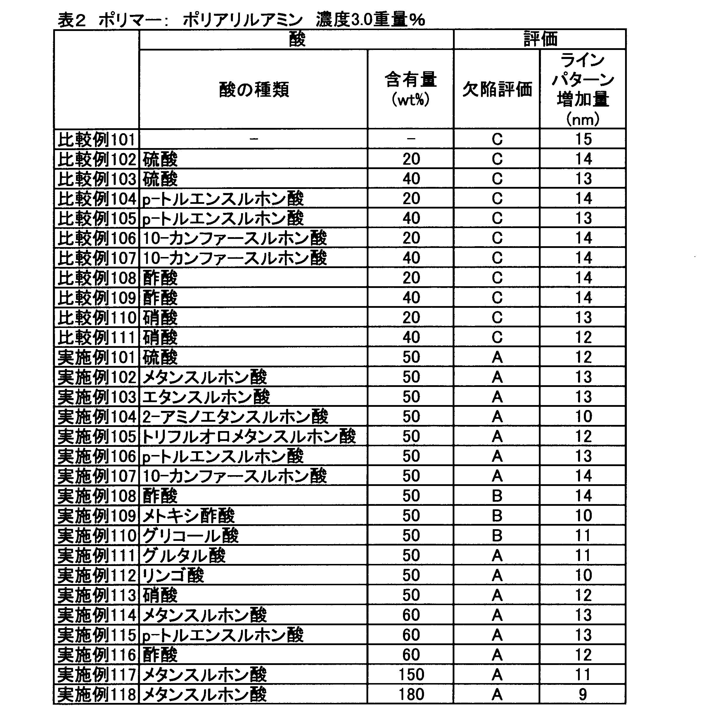
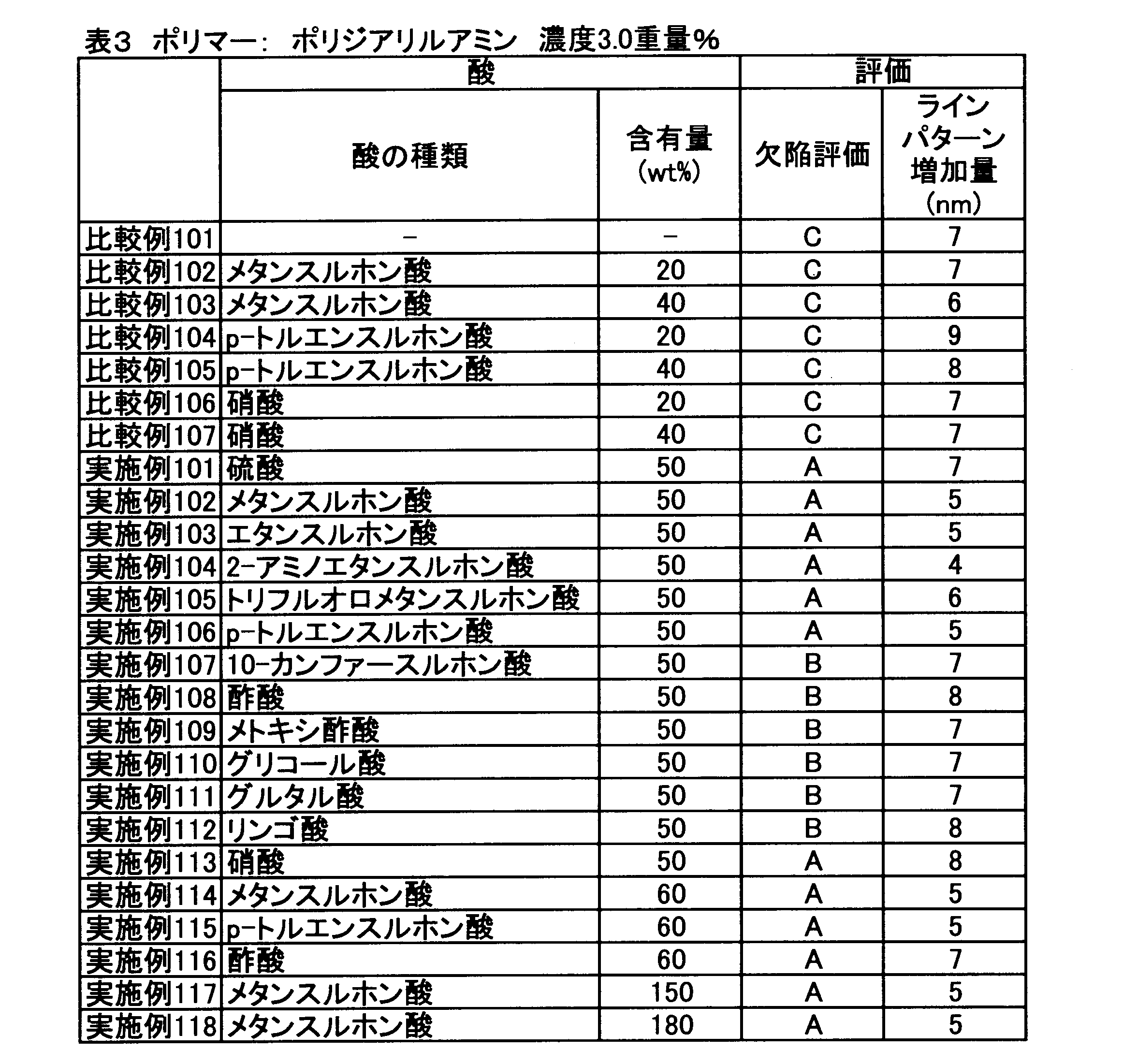
- the types of polymers, acids, and acids were blended in the amounts shown in Tables 1-5.
- the prepared composition was applied to the resist pattern 1 using a spin coater, heated at 140 ° C. for 60 seconds, washed with pure water, and dried.
- the dimension of the obtained line pattern was measured, and the increase amount of the line pattern by the composition for fine pattern formation was measured.
- the amount of increase in the line pattern means a value obtained by subtracting the line width of the pattern before processing from the line width of the pattern after processing with the fine pattern forming composition.
- the defect state of the substrate on which the pattern was formed was observed by KLA (manufactured by KLA Tencor) and evaluated according to the following evaluation criteria.
- Resist pattern formation example 2 Apply a lower antireflection film AZ ArF-1C5D (trade name, manufactured by AZ Electronic Materials Co., Ltd.) to an 8-inch silicon wafer with a spin coater (manufactured by Tokyo Electron Co., Ltd.), and bake at 200 ° C. for 60 seconds. The antireflection film having a thickness of 37 nm was obtained.
- a photosensitive resin composition AZ AX2110P (trade name, manufactured by AZ Electronic Materials Co., Ltd.) was baked at 110 ° C. for 60 seconds to obtain a film thickness of 120 nm.
- composition for forming fine resist pattern (II) The following polymers were prepared.
- Polyacrylic acid (weight average molecular weight 38,000) Polyoxyethylene (weight average molecular weight 95,000) Polyvinylamine (weight average molecular weight 25,000) Polyallylamine (weight average molecular weight 25,000) Polyvinylimidazole (weight average molecular weight 70,000) Polyethyleneimine (weight average molecular weight 10,000, polyethyleneimine 10000 (trade name, manufactured by Junsei Chemical Co., Ltd.)
- the above polymer, surfactant and methanesulfonic acid were dissolved in water to prepare a composition for forming a fine resist pattern containing the polymer at a concentration of 3% by weight.
- the blending ratio of the polymer, the acid content, and the pH were as shown in Table 6.
Landscapes
- Physics & Mathematics (AREA)
- General Physics & Mathematics (AREA)
- Chemical & Material Sciences (AREA)
- Spectroscopy & Molecular Physics (AREA)
- Organic Chemistry (AREA)
- Wood Science & Technology (AREA)
- Materials Engineering (AREA)
- Engineering & Computer Science (AREA)
- Life Sciences & Earth Sciences (AREA)
- Inorganic Chemistry (AREA)
- Photosensitive Polymer And Photoresist Processing (AREA)
- Exposure Of Semiconductors, Excluding Electron Or Ion Beam Exposure (AREA)
- Materials For Photolithography (AREA)
- Chemical Kinetics & Catalysis (AREA)
Abstract
Description
(1)形成されたレジストパターンを酸によって架橋しえる組成物で覆い、加熱によりレジストパターン中に存在する酸を拡散させ、レジストとの界面に架橋層をレジストパターンの被覆層として形成させ、現像液で非架橋部分を取り除くことでレジストパターンを太らせ、レジストパターンのホール径または分離幅が微細化される方法(特許文献1および2参照)。
(2)形成されたレジストパターンに、(メタ)アクリル酸モノマーと水溶性ビニルモノマーとからなるコポリマーの水溶液をレジストパターンに塗布し、熱処理により、レジストパターンを熱収縮させてパターンを微細化させる方法(特許文献3参照)。
(3)アミノ基、特に1級アミンを含むポリマーを含有する、フォトレジストパターンを被覆するための水溶性被覆用組成物(特許文献4参照)。
繰り返し単位中にアミノ基を含むポリマーと、
溶剤と
前記ポリマーの重量を基準として50重量%を超える酸と
を含んでなることを特徴とするものである。
繰り返し単位中にアミノ基を含むポリマーAと、
前記ポリマーAとは異なるポリマーであって、繰り返し単位中にアミノ基を含んでいても、含んでいなくてもよいポリマーBと、
溶剤と、
前記組成物中に含まれる、繰り返し単位中にアミノ基を含むポリマーの合計重量を基準として10重量%を超える酸と、
を含んでなり、
前記ポリマーAおよび前記ポリマーBのハンセン溶解度パラメーターから決定されるHSP距離が3以上であることを特徴とするものである。
繰り返し単位中にアミノ基を含むポリマーAと、
前記ポリマーAとは異なるポリマーであって、繰り返し単位中にアミノ基を含んでいても、含んでいなくてもよいポリマーBと、
溶剤と、
を含んでなり、
前記組成物のpHが5~10であり、
前記ポリマーAおよび前記ポリマーBのハンセン溶解度パラメーターから決定されるHSP距離が3以上であることを特徴とする組成物。
半導体基板上に化学増幅型フォトレジスト組成物を塗布してフォトレジスト層を形成する工程、
前記フォトレジスト層で被覆された前記半導体基板を露光する工程、
前記露光後に有機溶剤現像液で現像してフォトレジストパターンを形成する工程、
前記フォトレジストパターンの表面に、繰り返し単位中にアミノ基を含むポリマーと、前記ポリマーの重量を基準として50重量%を超える酸と、溶剤とを含んでなる微細パターン形成用組成物を塗布する工程、
塗布済みのフォトレジストパターンを加熱する工程、および
過剰の微細パターン形成用組成物を洗浄して除去する工程
を含んでなることを特徴とするものである。
半導体基板上に化学増幅型フォトレジスト組成物を塗布してフォトレジスト層を形成する工程、
前記フォトレジスト層で被覆された前記半導体基板を露光する工程、
前記露光後に有機溶剤現像液で現像する工程、
前記フォトレジストパターンの表面に、微細パターン形成用組成物を塗布する工程、
塗布済みのフォトレジストパターンを加熱する工程、および
過剰の微細パターン形成用組成物洗浄して除去する工程
を含んでなり、
前記微細パターン形成用組成物が、
繰り返し単位中にアミノ基を含むポリマーAと、
前記ポリマーAとは異なるポリマーであって、繰り返し単位中にアミノ基を含んでいても、含んでいなくてもよいポリマーBと、
溶剤と、
前記組成物中に含まれる、繰り返し単位中にアミノ基を含むポリマーの合計重量を基準として10重量%を超える酸と
を含んでなり、
前記ポリマーAおよび前記ポリマーBのハンセン溶解度パラメーターから決定されるHSP距離が3以上である
ことを特徴とするものである。
半導体基板上に化学増幅型フォトレジスト組成物を塗布してフォトレジスト層を形成する工程、
前記フォトレジスト層で被覆された前記半導体基板を露光する工程、
前記露光後に有機溶剤現像液で現像する工程、
前記フォトレジストパターンの表面に、微細パターン形成用組成物を塗布する工程、
塗布済みのフォトレジストパターンを加熱する工程、および
過剰の微細パターン形成用組成物洗浄して除去する工程
を含んでなり、
前記微細パターン形成用組成物が、
繰り返し単位中にアミノ基を含むポリマーAと、
前記ポリマーAとは異なるポリマーであって、繰り返し単位中にアミノ基を含んでいても、含んでいなくてもよいポリマーBと、
溶剤と、
を含んでなり、
前記組成物のpHが5~10であり、
前記ポリマーAおよび前記ポリマーBのハンセン溶解度パラメーターから決定されるHSP距離が3以上である
ことを特徴とするものである。
本発明による微細パターン形成用組成物は、繰り返し単位中にアミノ基を含むポリマーと、溶剤と、酸とを含んでなる。本発明において用いられるポリマーは、アミノ基を含むものである。ここでアミノ基は、第一級アミノ基(-NH2)、第二級アミノ基(-NHR)、および第3級アミノ基(-NRR’)をいう。ここで、アミノ基には、-N=のように窒素が二重結合を介して隣接元素に結合しているものも包含するものとする。これらのアミノ基は、繰り返し単位の側鎖に含まれていてもよいし、ポリマーの主鎖構造中に含まれていてもよい。
本発明による第二の微細パターン形成用組成物は、ポリマーAと、ポリマーAとは異なるポリマーBと、溶剤と、酸とを含んでなる。ここで、ポリマーAは、前記した第一の微細パターン形成用組成物の項で説明したアミノ基含有ポリマーである。そして、ポリマーBはポリマーAとは異なるものであり、ポリマーAとポリマーBとは極性に差がある。なお、ポリマーBは、ポリマーAと構造が異なることが必要であるが、アミノ基を含んでいても含まなくてもよい。
HSP距離=[(δDA-δDB)2+(δPA-δPB)2+(δHA-δHB)2]1/2
により極性の差が決定できる。本発明による第二の微細パターン形成用組成物におけるポリマーAとポリマーBのHSP距離は、3以上、好ましくは4以上である。
δD: 分子間の分散力に由来するエネルギー
δP: 分子間の極性力に由来するエネルギー
δH: 分子間の水素結合力に由来するエネルギー
物質名 (δD、δP、δH)
ポリビニルアミン (14.3, 7.8, 13.4)
ポリアリルアミン (14.8, 6.4, 11.2)
ポリビニルイミダゾール (20.1, 16.1, 10.8)
ポリメタクリル酸 (16.7, 6.0, 12.4)
ポリエチレンイミン (16.6, 6.0, 8.6)
ポリアミドアミン (19.9, 9.8, 10.6)
ポリアクリル酸エチル (16.3, 3.3, 6.8)
ポリアクリル酸プロピル (16.3, 2.6, 6.3)
ポリアクリロイルモルホリン (18.5, 8.8, 10.0)
ポリビニルオキサゾリン (17.9, 8.4, 0.0)
ポリビニルピロリドン (16.9, 10.3, 7.3)
ポリアリルアミン 2.66
ポリビニルイミダゾール 10.45
ポリメタクリル酸 3.16
ポリエチレンイミン 5.62
ポリアミドアミン 6.57
ポリアクリル酸エチル 8.23
ポリアクリル酸プロピル 9.02
ポリアクリロイルモルホリン 5.50
ポリビニルオキサゾリン 13.89
ポリビニルピロリドン 7.09
本発明による第三の微細パターン形成用組成物は、本発明による第二の微細パターン形成用組成物は、ポリマーAと、ポリマーAとは異なるポリマーBと、溶剤とを含んでなる。ここで、ポリマーおよび溶剤は、第二の微細パターン形成用組成物と同様のものから選択され、また含有率も同様の範囲から選択される。ただし、酸の含有量は限定されず、pHが限定されている点で異なっている。すなわち、第三の微細パターン形成用組成物においては、pHが5以上10以下であることが必要であり、6以上9.5以下であることが好ましい。pHをこのような範囲に調整するのに酸を用いることができるが、そのときに用いられる酸の含有量は第二の微細パターン形成用組成物で必須とされている含有量よりも低くてもよい。すなわち、酸の含有量は、組成物中に含まれる、繰り返し単位中にアミノ基を含むポリマーの合計重量を基準として、好ましくは10重量%以上、より好ましくは20重量%以上、特に好ましくは30重量%以上であるが、酸の含有量が相対的に低くても、pHが特定の範囲にあることで本発明の効果を得ることができる。
次に、本発明による微細なレジストパターンの形成方法について説明する。本発明の微細パターン形成用組成物が適用される代表的なパターン形成方法をあげると、次のような方法が挙げられる。
アミド系溶剤としては、N-メチル-2-ピロリドン、N,N-ジメチルアセトアミド、N,N-ジメチルホルムアミド等が使用できる。
スピンコーター(東京エレクトロン株式会社製)にて、下層反射防止膜AZ ArF-1C5D(商品名、AZエレクトロニックマテリアルズ株式会社製)を8インチシリコンウェハーに塗布し、200℃にて、60秒間ベークを行い、膜厚37nmの反射防止膜を得た。その上に感光性樹脂組成物AZ AX2110P(商品名、AZエレクトロニックマテリアルズ株式会社製)を、110℃にて60秒間ベークを行い120nmの膜厚を得た。得られたウェハーをArF線(193nm)の露光波長を有する露光装置(株式会社ニコン製)を用いて、マスク(ライン/スペース=1/1)を用いて、パターン露光を行った。その後110℃にて、60秒間ベークした後、2-ヘプタノンにて30秒間現像処理(ネガ型現像)を行い、ピッチ160nm、ライン幅80nmのレジストパターンを得た。
下記のポリマーを準備した。
ポリビニルアミン(重量平均分子量25,000)
ポリアリルアミン(重量平均分子量25,000)
ポリジアリルアミン(重量平均分子量5,000)
ポリエチレンイミン(重量平均分子量10,000、ポリエチレンイミン10000(商品名、純正化学株式会社製)
ポリ(アリルアミン-co-ジアリルアミン)(重量平均分子量30,000、アルリアミンとジアリルアミンの配合比は1:1(モル比)である)

調製された組成物をレジストパターン1にスピンコーターを用いて塗布し、140℃で60秒間加熱したのち、純水によって洗浄し、乾燥した。得られたラインパターンの寸法を測定し、微細パターン形成用組成物によるラインパターンの増加量を測定した。ラインパターンの増加量とは、微細化パターン形成用組成物で処理された後のパターンのライン幅から処理前のパターンのライン幅を減じたものを意味する。
A) ディフェクトの発生は見られておらず、半導体素子の製造に支障はない。
B) ディフェクトの発生は見られるが。半導体素子の製造に支障はない
C) ディフェクトの発生が顕著にみられ、半導体素子を製造するにあたり、支障をきたすものである。



スピンコーター(東京エレクトロン株式会社製)にて、下層反射防止膜AZ ArF-1C5D(商品名、AZエレクトロニックマテリアルズ株式会社製)を8インチシリコンウェハーに塗布し、200℃にて、60秒間ベークを行い、膜厚37nmの反射防止膜を得た。その上に感光性樹脂組成物AZ AX2110P(商品名、AZエレクトロニックマテリアルズ株式会社製)を、110℃にて60秒間ベークを行い120nmの膜厚を得た。得られたウェハーをArF線(193nm)の露光波長を有する露光装置(株式会社ニコン製)を用いて、粗密なパターンを有するマスク(ライン/スペース=1/1および3/1)を用いて、その後110℃にて、60秒間ベークした後、2-ヘプタノンにて30秒間現像処理(ネガ型現像)を行い、密なパターン(ピッチ160nm、ライン幅80nmのレジストパターン)及び疎なパターン(ピッチ320nm、ライン幅240nmのレジストパターン)を得た。
下記のポリマーを準備した。
ポリアクリル酸 (重量平均分子量38,000)
ポリオキシエチレン (重量平均分子量95,000)
ポリビニルアミン(重量平均分子量25,000)
ポリアリルアミン(重量平均分子量25,000)
ポリビニルイミダゾール(重量平均分子量70,000)
ポリエチレンイミン(重量平均分子量10,000、ポリエチレンイミン10000(商品名、純正化学株式会社製)
調製された組成物を、粗密のあるレジストパターンにスピンコーターを用いて塗布し、140℃で60秒間加熱したのち、純水によって洗浄し、乾燥した。その後パターン縮小量を測定し、パターン上の欠陥を観察した。得られた結果は表6に示すとおりであった。なお、表中、Xはレジストパターンが密な部分におけるライン幅の増加量であり、Yはレジストパターンが疎な部分におけるライン幅の増加量である。

Claims (15)
- 化学増幅型レジスト組成物を用いて形成したネガ型レジストパターンに適用し、レジストパターンを太らせることによってパターンを微細化するために用いられる微細パターン形成用組成物であって、
繰り返し単位中にアミノ基を含むポリマーと、
溶剤と
前記ポリマーの重量を基準として50重量%を超える酸と
を含んでなることを特徴とする組成物。 - 化学増幅型レジスト組成物を用いて形成したネガ型レジストパターンに適用し、レジストパターンを太らせることによってパターンを微細化するために用いられる微細パターン形成用組成物であって、
繰り返し単位中にアミノ基を含むポリマーAと、
前記ポリマーAとは異なるポリマーであって、繰り返し単位中にアミノ基を含んでいても、含んでいなくてもよいポリマーBと、
溶剤と、
前記組成物中に含まれる、繰り返し単位中にアミノ基を含むポリマーの合計重量を基準として10重量%を超える酸と
を含んでなり、
前記ポリマーAおよび前記ポリマーBのハンセン溶解度パラメーターから決定されるHSP距離が3以上であることを特徴とする組成物。 - 化学増幅型レジスト組成物を用いて形成したネガ型レジストパターンに適用し、レジストパターンを太らせることによってパターンを微細化するために用いられる微細パターン形成用組成物であって、
繰り返し単位中にアミノ基を含むポリマーAと、
前記ポリマーAとは異なるポリマーであって、繰り返し単位中にアミノ基を含んでいても、含んでいなくてもよいポリマーBと、
溶剤と
を含んでなり、
前記組成物のpHが5~10であり、
前記ポリマーAおよび前記ポリマーBのハンセン溶解度パラメーターから決定されるHSP距離が3以上であることを特徴とする組成物。 - 前記アミノ基が、第一級アミノ基または第二級アミノ基である、請求項1~3のいずれか1項に記載の組成物。
- 前記繰り返し単位が、アリルアミン単位、ジアリルアミン単位、およびエチレンイミン単位からなる群から選択されるものである、請求項1~3のいずれか1項に記載の組成物。
- 前記ポリマーが、ポリビニルアミン、ポリアリルアミン、ポリジアリルアミン、ポリエチレンイミン、およびポリ(アリルアミン-co-ジアリルアミン)からなる群から選択される、請求項1~3のいずれか1項に記載の組成物。
- 前記酸が、スルホン酸、カルボン酸、硫酸、硝酸、およびそれらの混合物からなる群から選択される、請求項1~6のいずれか1項に記載の組成物。
- 前記スルホン酸が、メタンスルホン酸、エタンスルホン酸、2-アミノメタンスルホン酸、トリフルオロメタンスルホン酸、p-トルエンスルホン酸、および10-カンファースルホン酸からなる群から選択されるものである、請求項7に記載の組成物。
- 前記カルボン酸が、酢酸、メトキシ酢酸、グリコール酸、グルタル酸、リンゴ酸からなる群から選択されるものである、請求項7に記載の組成物。
- 前記溶剤が水を含んでなる、請求項1~9のいずれか1項に記載の組成物。
- 界面活性剤をさらに含んでなる、請求項1~10のいずれか1項に記載の組成物。
- 半導体基板上に化学増幅型フォトレジスト組成物を塗布してフォトレジスト層を形成する工程、
前記フォトレジスト層で被覆された前記半導体基板を露光する工程、
前記露光後に有機溶剤現像液で現像する工程、
前記フォトレジストパターンの表面に、繰り返し単位中にアミノ基を含むポリマーと、前記ポリマーの重量を基準として50重量%を超える酸と、溶剤とを含んでなる微細パターン形成用組成物を塗布する工程、
塗布済みのフォトレジストパターンを加熱する工程、および
過剰の微細パターン形成用組成物洗浄して除去する工程
を含んでなることを特徴とする微細化されたネガ型レジストパターンの形成方法。 - 半導体基板上に化学増幅型フォトレジスト組成物を塗布してフォトレジスト層を形成する工程、
前記フォトレジスト層で被覆された前記半導体基板を露光する工程、
前記露光後に有機溶剤現像液で現像する工程、
前記フォトレジストパターンの表面に、微細パターン形成用組成物を塗布する工程、
塗布済みのフォトレジストパターンを加熱する工程、および
過剰の微細パターン形成用組成物洗浄して除去する工程
を含んでなり、
前記微細パターン形成用組成物が、
繰り返し単位中にアミノ基を含むポリマーAと、
前記ポリマーAとは異なるポリマーであって、繰り返し単位中にアミノ基を含んでいても、含んでいなくてもよいポリマーBと、
溶剤と
前記組成物中に含まれる、繰り返し単位中にアミノ基を含むポリマーの合計重量を基準として10重量%を超える酸と
を含んでなり、
前記ポリマーAおよび前記ポリマーBのハンセン溶解度パラメーターから決定されるHSP距離が3以上である
ことを特徴とする微細化されたネガ型レジストパターンの形成方法。 - 半導体基板上に化学増幅型フォトレジスト組成物を塗布してフォトレジスト層を形成する工程、
前記フォトレジスト層で被覆された前記半導体基板を露光する工程、
前記露光後に有機溶剤現像液で現像する工程、
前記フォトレジストパターンの表面に、微細パターン形成用組成物を塗布する工程、
塗布済みのフォトレジストパターンを加熱する工程、および
過剰の微細パターン形成用組成物洗浄して除去する工程
を含んでなり、
前記微細パターン形成用組成物が、
繰り返し単位中にアミノ基を含むポリマーAと、
前記ポリマーAとは異なるポリマーであって、繰り返し単位中にアミノ基を含んでいても、含んでいなくてもよいポリマーBと、
溶剤と、
を含んでなり、
前記組成物のpHが5~10であり、
前記ポリマーAおよび前記ポリマーBのハンセン溶解度パラメーターから決定されるHSP距離が3以上である
ことを特徴とする微細化されたネガ型レジストパターンの形成方法。 - 前記フォトレジスト組成物が、光酸発生剤をさらに含んでなる、請求項12~14のいずれか1項に記載の微細化されたネガ型レジストパターンの形成方法。
Priority Applications (6)
| Application Number | Priority Date | Filing Date | Title |
|---|---|---|---|
| CN201480008277.7A CN104995564B (zh) | 2013-02-26 | 2014-02-26 | 微细抗蚀图案形成用组合物以及使用其的图案形成方法 |
| KR1020157026718A KR101900660B1 (ko) | 2013-02-26 | 2014-02-26 | 미세 레지스트 패턴 형성용 조성물 및 이를 사용한 패턴 형성 방법 |
| US14/768,660 US9921481B2 (en) | 2013-02-26 | 2014-02-26 | Fine resist pattern-forming composition and pattern forming method using same |
| SG11201505632YA SG11201505632YA (en) | 2013-02-26 | 2014-02-26 | Fine resist pattern-forming composition and pattern forming method using same |
| EP14756352.2A EP2963499A4 (en) | 2013-02-26 | 2014-02-26 | Fine resist pattern-forming composition and pattern forming method using same |
| IL240745A IL240745B (en) | 2013-02-26 | 2015-08-20 | A preparation for creating a fine pattern of resist and a method for creating a pattern using it |
Applications Claiming Priority (2)
| Application Number | Priority Date | Filing Date | Title |
|---|---|---|---|
| JP2013036029A JP6239833B2 (ja) | 2013-02-26 | 2013-02-26 | 微細レジストパターン形成用組成物およびそれを用いたパターン形成方法 |
| JP2013-036029 | 2013-02-26 |
Publications (1)
| Publication Number | Publication Date |
|---|---|
| WO2014132992A1 true WO2014132992A1 (ja) | 2014-09-04 |
Family
ID=51428254
Family Applications (1)
| Application Number | Title | Priority Date | Filing Date |
|---|---|---|---|
| PCT/JP2014/054657 Ceased WO2014132992A1 (ja) | 2013-02-26 | 2014-02-26 | 微細レジストパターン形成用組成物およびそれを用いたパターン形成方法 |
Country Status (9)
| Country | Link |
|---|---|
| US (1) | US9921481B2 (ja) |
| EP (1) | EP2963499A4 (ja) |
| JP (1) | JP6239833B2 (ja) |
| KR (1) | KR101900660B1 (ja) |
| CN (1) | CN104995564B (ja) |
| IL (1) | IL240745B (ja) |
| SG (2) | SG10201708724WA (ja) |
| TW (1) | TWI616480B (ja) |
| WO (1) | WO2014132992A1 (ja) |
Cited By (6)
| Publication number | Priority date | Publication date | Assignee | Title |
|---|---|---|---|---|
| JP2016035576A (ja) * | 2014-07-31 | 2016-03-17 | ローム アンド ハース エレクトロニック マテリアルズ エルエルシーRohm and Haas Electronic Materials LLC | パターン収縮法 |
| CN107077081A (zh) * | 2014-10-14 | 2017-08-18 | Az电子材料(卢森堡)有限公司 | 抗蚀图案处理用组合物以及使用其的图案形成方法 |
| JP2018005199A (ja) * | 2016-07-08 | 2018-01-11 | 東京応化工業株式会社 | レジストパターン厚肉化用ポリマー組成物、及びレジストパターン形成方法 |
| WO2020210660A1 (en) * | 2019-04-12 | 2020-10-15 | Inpria Corporation | Organometallic photoresist developer compositions and processing methods |
| US11480874B2 (en) | 2018-10-17 | 2022-10-25 | Inpria Corporation | Patterned organometallic photoresists and methods of patterning |
| US11947262B2 (en) | 2020-03-02 | 2024-04-02 | Inpria Corporation | Process environment for inorganic resist patterning |
Families Citing this family (8)
| Publication number | Priority date | Publication date | Assignee | Title |
|---|---|---|---|---|
| JP6157151B2 (ja) * | 2013-03-05 | 2017-07-05 | アーゼッド・エレクトロニック・マテリアルズ(ルクセンブルグ)ソシエテ・ア・レスポンサビリテ・リミテ | 微細レジストパターン形成用組成物およびそれを用いたパターン形成方法 |
| KR102609535B1 (ko) * | 2015-07-08 | 2023-12-04 | 주식회사 동진쎄미켐 | 포토레지스트 패턴 코팅용 조성물 및 이를 이용한 미세 패턴 형성 방법 |
| TWI738775B (zh) | 2016-05-13 | 2021-09-11 | 日商住友化學股份有限公司 | 光阻組成物及製造光阻圖案之方法 |
| JP6969889B2 (ja) | 2016-05-13 | 2021-11-24 | 住友化学株式会社 | レジスト組成物及びレジストパターンの製造方法 |
| JP7316022B2 (ja) | 2016-05-13 | 2023-07-27 | 住友化学株式会社 | レジスト組成物及びレジストパターンの製造方法 |
| TWI610392B (zh) * | 2016-09-05 | 2018-01-01 | Daxin Materials Corp. | 光電元件的製備方法 |
| CN111936588A (zh) * | 2018-04-06 | 2020-11-13 | 日产化学株式会社 | 涂布膜形成组合物和半导体装置的制造方法 |
| US11287740B2 (en) | 2018-06-15 | 2022-03-29 | Taiwan Semiconductor Manufacturing Co., Ltd. | Photoresist composition and method of forming photoresist pattern |
Citations (7)
| Publication number | Priority date | Publication date | Assignee | Title |
|---|---|---|---|---|
| JPH1073927A (ja) | 1996-07-05 | 1998-03-17 | Mitsubishi Electric Corp | 微細パターン形成材料及びこれを用いた半導体装置の製造方法並びに半導体装置 |
| JP2003084459A (ja) | 2001-07-05 | 2003-03-19 | Tokyo Ohka Kogyo Co Ltd | レジストパターン微細化用被覆形成剤及びそれを用いた微細レジストパターン形成方法 |
| JP2005300853A (ja) | 2004-04-09 | 2005-10-27 | Az Electronic Materials Kk | 水溶性樹脂組成物およびそれを用いたパターン形成方法 |
| JP2006048035A (ja) * | 2004-07-22 | 2006-02-16 | Samsung Electronics Co Ltd | 半導体素子製造用のマスクパターンとその形成方法、及び微細パターンを有する半導体素子の製造方法 |
| JP2008518260A (ja) | 2004-10-26 | 2008-05-29 | エイゼット・エレクトロニック・マテリアルズ・ユーエスエイ・コーポレイション | フォトレジストパターンを被覆するための組成物 |
| JP2008310314A (ja) * | 2007-05-15 | 2008-12-25 | Fujifilm Corp | パターン形成方法 |
| JP2013003155A (ja) * | 2011-06-10 | 2013-01-07 | Tokyo Ohka Kogyo Co Ltd | レジストパターン形成方法 |
Family Cites Families (12)
| Publication number | Priority date | Publication date | Assignee | Title |
|---|---|---|---|---|
| JP2001228616A (ja) * | 2000-02-16 | 2001-08-24 | Mitsubishi Electric Corp | 微細パターン形成材料及びこれを用いた半導体装置の製造方法 |
| SG129274A1 (en) * | 2003-02-19 | 2007-02-26 | Mitsubishi Gas Chemical Co | Cleaaning solution and cleaning process using the solution |
| JP2005022282A (ja) * | 2003-07-03 | 2005-01-27 | Fuji Photo Film Co Ltd | シリカ予分散液、シリカ微粒化分散液、インク受容層塗布液及びインクジェット記録媒体 |
| KR100585138B1 (ko) * | 2004-04-08 | 2006-05-30 | 삼성전자주식회사 | 반도체 소자 제조용 마스크 패턴 및 그 형성 방법과 미세패턴을 가지는 반도체 소자의 제조 방법 |
| JP4566862B2 (ja) * | 2005-08-25 | 2010-10-20 | 富士通株式会社 | レジストパターン厚肉化材料、レジストパターンの形成方法、半導体装置及びその製造方法 |
| JP4554665B2 (ja) * | 2006-12-25 | 2010-09-29 | 富士フイルム株式会社 | パターン形成方法、該パターン形成方法に用いられる多重現像用ポジ型レジスト組成物、該パターン形成方法に用いられるネガ現像用現像液及び該パターン形成方法に用いられるネガ現像用リンス液 |
| JP5520590B2 (ja) * | 2009-10-06 | 2014-06-11 | 富士フイルム株式会社 | パターン形成方法、化学増幅型レジスト組成物及びレジスト膜 |
| JP5553210B2 (ja) * | 2010-04-01 | 2014-07-16 | ブラザー工業株式会社 | インクジェット記録用の処理液、インクセットおよびインクジェット記録方法 |
| US8852848B2 (en) | 2010-07-28 | 2014-10-07 | Z Electronic Materials USA Corp. | Composition for coating over a photoresist pattern |
| JP5785121B2 (ja) * | 2011-04-28 | 2015-09-24 | 信越化学工業株式会社 | パターン形成方法 |
| JP5705669B2 (ja) * | 2011-07-14 | 2015-04-22 | メルクパフォーマンスマテリアルズIp合同会社 | 微細パターン形成用組成物およびそれを用いた微細化されたパターン形成方法 |
| JP5846889B2 (ja) * | 2011-12-14 | 2016-01-20 | 東京応化工業株式会社 | レジスト組成物、レジストパターン形成方法、化合物 |
-
2013
- 2013-02-26 JP JP2013036029A patent/JP6239833B2/ja active Active
-
2014
- 2014-02-25 TW TW103106175A patent/TWI616480B/zh active
- 2014-02-26 EP EP14756352.2A patent/EP2963499A4/en not_active Withdrawn
- 2014-02-26 SG SG10201708724WA patent/SG10201708724WA/en unknown
- 2014-02-26 KR KR1020157026718A patent/KR101900660B1/ko active Active
- 2014-02-26 WO PCT/JP2014/054657 patent/WO2014132992A1/ja not_active Ceased
- 2014-02-26 US US14/768,660 patent/US9921481B2/en not_active Expired - Fee Related
- 2014-02-26 SG SG11201505632YA patent/SG11201505632YA/en unknown
- 2014-02-26 CN CN201480008277.7A patent/CN104995564B/zh active Active
-
2015
- 2015-08-20 IL IL240745A patent/IL240745B/en active IP Right Grant
Patent Citations (7)
| Publication number | Priority date | Publication date | Assignee | Title |
|---|---|---|---|---|
| JPH1073927A (ja) | 1996-07-05 | 1998-03-17 | Mitsubishi Electric Corp | 微細パターン形成材料及びこれを用いた半導体装置の製造方法並びに半導体装置 |
| JP2003084459A (ja) | 2001-07-05 | 2003-03-19 | Tokyo Ohka Kogyo Co Ltd | レジストパターン微細化用被覆形成剤及びそれを用いた微細レジストパターン形成方法 |
| JP2005300853A (ja) | 2004-04-09 | 2005-10-27 | Az Electronic Materials Kk | 水溶性樹脂組成物およびそれを用いたパターン形成方法 |
| JP2006048035A (ja) * | 2004-07-22 | 2006-02-16 | Samsung Electronics Co Ltd | 半導体素子製造用のマスクパターンとその形成方法、及び微細パターンを有する半導体素子の製造方法 |
| JP2008518260A (ja) | 2004-10-26 | 2008-05-29 | エイゼット・エレクトロニック・マテリアルズ・ユーエスエイ・コーポレイション | フォトレジストパターンを被覆するための組成物 |
| JP2008310314A (ja) * | 2007-05-15 | 2008-12-25 | Fujifilm Corp | パターン形成方法 |
| JP2013003155A (ja) * | 2011-06-10 | 2013-01-07 | Tokyo Ohka Kogyo Co Ltd | レジストパターン形成方法 |
Non-Patent Citations (2)
| Title |
|---|
| EMMANUEL STEFANIS; COSTAS PANAYIOTOU, INT. J. THERMOPHYS, vol. 29, 2008, pages 568 - 585 |
| See also references of EP2963499A4 |
Cited By (9)
| Publication number | Priority date | Publication date | Assignee | Title |
|---|---|---|---|---|
| JP2016035576A (ja) * | 2014-07-31 | 2016-03-17 | ローム アンド ハース エレクトロニック マテリアルズ エルエルシーRohm and Haas Electronic Materials LLC | パターン収縮法 |
| CN107077081A (zh) * | 2014-10-14 | 2017-08-18 | Az电子材料(卢森堡)有限公司 | 抗蚀图案处理用组合物以及使用其的图案形成方法 |
| JP2018005199A (ja) * | 2016-07-08 | 2018-01-11 | 東京応化工業株式会社 | レジストパターン厚肉化用ポリマー組成物、及びレジストパターン形成方法 |
| US11480874B2 (en) | 2018-10-17 | 2022-10-25 | Inpria Corporation | Patterned organometallic photoresists and methods of patterning |
| US12399426B2 (en) | 2018-10-17 | 2025-08-26 | Inpria Corporation | Patterned organometallic photoresists and methods of patterning |
| WO2020210660A1 (en) * | 2019-04-12 | 2020-10-15 | Inpria Corporation | Organometallic photoresist developer compositions and processing methods |
| US12416861B2 (en) | 2019-04-12 | 2025-09-16 | Inpria Corporation | Organometallic photoresist developer compositions and processing methods |
| US11947262B2 (en) | 2020-03-02 | 2024-04-02 | Inpria Corporation | Process environment for inorganic resist patterning |
| US12498641B2 (en) | 2020-03-02 | 2025-12-16 | Inpria Corporation | Process environment for inorganic resist patterning |
Also Published As
| Publication number | Publication date |
|---|---|
| JP6239833B2 (ja) | 2017-11-29 |
| CN104995564A (zh) | 2015-10-21 |
| SG11201505632YA (en) | 2015-08-28 |
| CN104995564B (zh) | 2019-12-10 |
| EP2963499A1 (en) | 2016-01-06 |
| TW201439184A (zh) | 2014-10-16 |
| KR101900660B1 (ko) | 2018-09-21 |
| EP2963499A4 (en) | 2017-08-02 |
| US20160002494A1 (en) | 2016-01-07 |
| KR20150125694A (ko) | 2015-11-09 |
| IL240745B (en) | 2018-05-31 |
| US9921481B2 (en) | 2018-03-20 |
| IL240745A0 (en) | 2015-10-29 |
| JP2014164177A (ja) | 2014-09-08 |
| TWI616480B (zh) | 2018-03-01 |
| SG10201708724WA (en) | 2017-12-28 |
Similar Documents
| Publication | Publication Date | Title |
|---|---|---|
| JP6239833B2 (ja) | 微細レジストパターン形成用組成物およびそれを用いたパターン形成方法 | |
| JP5758263B2 (ja) | 微細レジストパターン形成用組成物およびそれを用いたパターン形成方法 | |
| JP6157151B2 (ja) | 微細レジストパターン形成用組成物およびそれを用いたパターン形成方法 | |
| WO2013183686A1 (ja) | 上層膜形成用組成物およびそれを用いたレジストパターン形成方法 | |
| JP6790107B2 (ja) | 微細パターン形成用組成物およびそれを用いた微細パターン形成方法 | |
| JP2012137778A (ja) | ケイ素含有微細パターン形成用組成物 | |
| TW201535053A (zh) | 微細光阻圖案形成用組成物及使用其之圖案形成方法 |
Legal Events
| Date | Code | Title | Description |
|---|---|---|---|
| 121 | Ep: the epo has been informed by wipo that ep was designated in this application |
Ref document number: 14756352 Country of ref document: EP Kind code of ref document: A1 |
|
| WWE | Wipo information: entry into national phase |
Ref document number: 14768660 Country of ref document: US |
|
| WWE | Wipo information: entry into national phase |
Ref document number: 240745 Country of ref document: IL |
|
| NENP | Non-entry into the national phase |
Ref country code: DE |
|
| ENP | Entry into the national phase |
Ref document number: 20157026718 Country of ref document: KR Kind code of ref document: A |
|
| WWE | Wipo information: entry into national phase |
Ref document number: 2014756352 Country of ref document: EP |