WO2014136548A1 - 半導体装置 - Google Patents
半導体装置 Download PDFInfo
- Publication number
- WO2014136548A1 WO2014136548A1 PCT/JP2014/053410 JP2014053410W WO2014136548A1 WO 2014136548 A1 WO2014136548 A1 WO 2014136548A1 JP 2014053410 W JP2014053410 W JP 2014053410W WO 2014136548 A1 WO2014136548 A1 WO 2014136548A1
- Authority
- WO
- WIPO (PCT)
- Prior art keywords
- region
- drain
- wiring
- source
- nmos transistor
- Prior art date
- Legal status (The legal status is an assumption and is not a legal conclusion. Google has not performed a legal analysis and makes no representation as to the accuracy of the status listed.)
- Ceased
Links
Images


Classifications
-
- H—ELECTRICITY
- H10—SEMICONDUCTOR DEVICES; ELECTRIC SOLID-STATE DEVICES NOT OTHERWISE PROVIDED FOR
- H10D—INORGANIC ELECTRIC SEMICONDUCTOR DEVICES
- H10D89/00—Aspects of integrated devices not covered by groups H10D84/00 - H10D88/00
- H10D89/60—Integrated devices comprising arrangements for electrical or thermal protection, e.g. protection circuits against electrostatic discharge [ESD]
- H10D89/601—Integrated devices comprising arrangements for electrical or thermal protection, e.g. protection circuits against electrostatic discharge [ESD] for devices having insulated gate electrodes, e.g. for IGFETs or IGBTs
- H10D89/811—Integrated devices comprising arrangements for electrical or thermal protection, e.g. protection circuits against electrostatic discharge [ESD] for devices having insulated gate electrodes, e.g. for IGFETs or IGBTs using FETs as protective elements
- H10D89/813—Integrated devices comprising arrangements for electrical or thermal protection, e.g. protection circuits against electrostatic discharge [ESD] for devices having insulated gate electrodes, e.g. for IGFETs or IGBTs using FETs as protective elements specially adapted to provide an electrical current path other than the field-effect induced current path
-
- H—ELECTRICITY
- H10—SEMICONDUCTOR DEVICES; ELECTRIC SOLID-STATE DEVICES NOT OTHERWISE PROVIDED FOR
- H10D—INORGANIC ELECTRIC SEMICONDUCTOR DEVICES
- H10D64/00—Electrodes of devices having potential barriers
- H10D64/20—Electrodes characterised by their shapes, relative sizes or dispositions
- H10D64/23—Electrodes carrying the current to be rectified, amplified, oscillated or switched, e.g. sources, drains, anodes or cathodes
- H10D64/251—Source or drain electrodes for field-effect devices
- H10D64/257—Source or drain electrodes for field-effect devices for lateral devices wherein the source or drain electrodes are characterised by top-view geometrical layouts, e.g. interdigitated, semi-circular, annular or L-shaped electrodes
-
- H—ELECTRICITY
- H10—SEMICONDUCTOR DEVICES; ELECTRIC SOLID-STATE DEVICES NOT OTHERWISE PROVIDED FOR
- H10D—INORGANIC ELECTRIC SEMICONDUCTOR DEVICES
- H10D89/00—Aspects of integrated devices not covered by groups H10D84/00 - H10D88/00
- H10D89/10—Integrated device layouts
-
- H—ELECTRICITY
- H10—SEMICONDUCTOR DEVICES; ELECTRIC SOLID-STATE DEVICES NOT OTHERWISE PROVIDED FOR
- H10D—INORGANIC ELECTRIC SEMICONDUCTOR DEVICES
- H10D89/00—Aspects of integrated devices not covered by groups H10D84/00 - H10D88/00
- H10D89/60—Integrated devices comprising arrangements for electrical or thermal protection, e.g. protection circuits against electrostatic discharge [ESD]
- H10D89/601—Integrated devices comprising arrangements for electrical or thermal protection, e.g. protection circuits against electrostatic discharge [ESD] for devices having insulated gate electrodes, e.g. for IGFETs or IGBTs
- H10D89/811—Integrated devices comprising arrangements for electrical or thermal protection, e.g. protection circuits against electrostatic discharge [ESD] for devices having insulated gate electrodes, e.g. for IGFETs or IGBTs using FETs as protective elements
- H10D89/813—Integrated devices comprising arrangements for electrical or thermal protection, e.g. protection circuits against electrostatic discharge [ESD] for devices having insulated gate electrodes, e.g. for IGFETs or IGBTs using FETs as protective elements specially adapted to provide an electrical current path other than the field-effect induced current path
- H10D89/814—Integrated devices comprising arrangements for electrical or thermal protection, e.g. protection circuits against electrostatic discharge [ESD] for devices having insulated gate electrodes, e.g. for IGFETs or IGBTs using FETs as protective elements specially adapted to provide an electrical current path other than the field-effect induced current path involving a parasitic bipolar transistor triggered by the electrical biasing of the gate electrode of the FET, e.g. gate coupled transistors
-
- H—ELECTRICITY
- H10—SEMICONDUCTOR DEVICES; ELECTRIC SOLID-STATE DEVICES NOT OTHERWISE PROVIDED FOR
- H10W—GENERIC PACKAGES, INTERCONNECTIONS, CONNECTORS OR OTHER CONSTRUCTIONAL DETAILS OF DEVICES COVERED BY CLASS H10
- H10W20/00—Interconnections in chips, wafers or substrates
- H10W20/40—Interconnections external to wafers or substrates, e.g. back-end-of-line [BEOL] metallisations or vias connecting to gate electrodes
- H10W20/41—Interconnections external to wafers or substrates, e.g. back-end-of-line [BEOL] metallisations or vias connecting to gate electrodes characterised by their conductive parts
- H10W20/43—Layouts of interconnections
-
- H—ELECTRICITY
- H10—SEMICONDUCTOR DEVICES; ELECTRIC SOLID-STATE DEVICES NOT OTHERWISE PROVIDED FOR
- H10W—GENERIC PACKAGES, INTERCONNECTIONS, CONNECTORS OR OTHER CONSTRUCTIONAL DETAILS OF DEVICES COVERED BY CLASS H10
- H10W20/00—Interconnections in chips, wafers or substrates
- H10W20/40—Interconnections external to wafers or substrates, e.g. back-end-of-line [BEOL] metallisations or vias connecting to gate electrodes
- H10W20/498—Resistive arrangements or effects of, or between, wiring layers
-
- H—ELECTRICITY
- H10—SEMICONDUCTOR DEVICES; ELECTRIC SOLID-STATE DEVICES NOT OTHERWISE PROVIDED FOR
- H10D—INORGANIC ELECTRIC SEMICONDUCTOR DEVICES
- H10D30/00—Field-effect transistors [FET]
- H10D30/60—Insulated-gate field-effect transistors [IGFET]
Definitions
- the present invention relates to a semiconductor device having an ESD protection circuit using an N-channel MOS transistor.
- a semiconductor device composed of a semiconductor integrated circuit has a pad which is an electrode for external connection.
- An ESD protection circuit for protecting the internal circuit of the semiconductor device from ESD (electrostatic discharge) is usually provided in the vicinity of the pad.
- One ESD protection circuit uses a multi-finger type N-channel MOS transistor (hereinafter referred to as NMOS transistor).
- NMOS transistor multi-finger type N-channel MOS transistor
- the gate and source of the NMOS transistor are connected to a ground terminal, and the drain is connected to a pad and an internal circuit (see, for example, Patent Document 1).
- FIG. 3 shows an example of a transistor in such a situation.
- the NMOS transistor 30 of the ESD protection circuit has a drain wiring 53a connected to the pad 40 and the internal circuit, and a gate 51 and a source wiring 52a connected to the ground wiring. As shown in FIG.
- the resistance value of the drain wiring 53a is the same as that of the source wiring 52a. It becomes lower than the resistance value.
- the generated surge current flows from the pad 40 to the ground terminal via the NMOS transistor 50.
- the surge current flows in order through a resistance represented by the drain wiring 53a, a resistance in the channel region under the gate 51, and a resistance represented by the source wiring 52a.
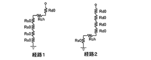
- the resistance of the drain wiring and the source wiring in one of the divided lengths is Rd0 and Rs0, and the path 1 is on the drain wiring 3a side (FIG. 3).
- the resistance components of path 1 and path 2 are as follows: Shown in
- the drain wiring resistance Rd0 includes all resistance components such as wiring metal resistance, contact resistance, and drain region resistance.
- the drain wiring width> the source wiring width, Rd0 ⁇ Rs0 and the resistance component of the path 1> the resistance component of the path 2 is established, so that the surge current flows more easily in the path 2 than in the path 1. That is, the surge current concentrates on the gate on the source wiring 52a side (the lower side in FIG. 3) in each finger. Therefore, the vicinity of the channel region of this portion is easily destroyed, and the ESD tolerance of the NMOS transistor 50 and the semiconductor device is lowered.
- This invention is made in view of the said subject, and provides a semiconductor device with high ESD tolerance.
- the present invention provides a multi-finger type semiconductor device having an NMOS transistor type ESD protection circuit, and a plurality of sources and a plurality of drains alternately arranged on a semiconductor substrate surface,
- the NMOS transistor having a plurality of channel regions arranged between the drain and a gate provided on the channel region; and provided on the gate and the source in the region of the NMOS transistor;
- a source wiring that electrically connects the gate, the source, and a ground terminal, and the drain that is provided on the drain in the region of the NMOS transistor and electrically connects the drain and a pad that is an external connection electrode.
- Wiring of the source wiring in the region of the NMOS transistor To provide a semiconductor device, characterized in that it comprises a drain wire, a having the same wire width as.
- FIG. 1 is a plan view showing an ESD protection circuit using an NMOS transistor.
- the NMOS transistor 30 is a multi-finger type, and a plurality of source regions 32 and a plurality of drain regions 33 are alternately arranged on the surface of the semiconductor substrate.
- the plurality of channel regions are arranged between the source region 32 and the drain region 33, and the gate electrode 31 is provided on the channel region.
- the source wiring 32 a is provided on the gate electrode 31 and the source region 32 in the region of the NMOS transistor 30.
- the source line 32a electrically connects the gate electrode 31, the source region 32, and the ground terminal.
- the drain wiring 33 a is provided on the drain region 33 in the region of the NMOS transistor 30 and is not provided on the gate electrode 31.
- the drain wiring 33a electrically connects the drain region 33 and the pad 20 (FIG. 2) which is an external connection electrode.
- the drain wiring 33a has the same wiring width as that of the source wiring 32a, and the arrangement of the contacts 34 is the same for both wirings.
- the source region, source wiring, drain region, and drain wiring sandwiching one gate electrode are referred to as one finger. Then, it is assumed that the NMOS transistor 30 is formed by folding one finger and continuously arranging the fingers in order.
- FIG. 2 is a circuit diagram showing an ESD protection circuit of the semiconductor device.
- the surge current is designed to flow from the pad 20 to the ground terminal via the ESD protection circuit.
- the NMOS transistor 30 causes this surge current to flow from the drain to the source by the bipolar operation triggered by the surface breakdown, so that the surge current flows through the NMOS transistor 30 and does not flow into the internal circuit.
- the internal circuit is protected from surge current.
- the surge current sequentially flows through the resistance of the drain wiring 33a, the resistance of the channel region under the gate 31, and the resistance of the source wiring 32a.
- one finger of the NMOS transistor 30 is equally divided into five in the channel width direction, the resistance of the drain wiring 33a in each region is Rd0, and the resistance of the channel region is Rch.
- the resistance of the source wiring is Rs0
- Resistance component of path 2 4Rd0 + Rch + 1Rs0
- the resistance component of path 1 is equal to the resistance component of path 2.
- the resistance of each part divided equally is equal.
- the total resistance value of the wiring resistance to the surge current is the same between the pad 20 and the ground terminal, regardless of the channel region where the surge current flows in one finger of the NMOS transistor 30. become. Then, the surge current does not concentrate on a specific part in the channel region. Therefore, the vicinity of the channel region in a specific portion is not easily destroyed, and the ESD tolerance of the NMOS transistor 30 and the semiconductor device is increased.
- the reason why the source wiring 32a is provided not only on the source region 32 but also on the gate electrode 31 is to avoid an increase in element size and a decrease in ESD tolerance.
- the same wiring width of the drain wiring 33a and the source wiring 32a contributes to the improvement of the ESD resistance.
- the wiring width of the drain wiring 33a and the source wiring 32a is ideally at least equal to that of the drain region 33.
- the source region 32 is too narrow to dispose the source wiring 32 a having the same width as the drain region 33 on the source region 32 having a width narrower than that of the drain region 33.
- One solution is to make the width of the source region 32 equal to the width of the drain region 33.
- this increases the element size and affects the increase in chip size. Therefore, without increasing the source region 32 and providing the source wiring 32a up to the gate 31 electrode, an increase in element size and a decrease in ESD tolerance can be avoided.
Landscapes
- Semiconductor Integrated Circuits (AREA)
- Metal-Oxide And Bipolar Metal-Oxide Semiconductor Integrated Circuits (AREA)
- Physics & Mathematics (AREA)
- Geometry (AREA)
- Insulated Gate Type Field-Effect Transistor (AREA)
- Engineering & Computer Science (AREA)
- General Engineering & Computer Science (AREA)
Abstract
Description
経路2の抵抗成分=4Rd0+Rch+1Rs0
この式で表される分割されたNMOSトランジスタの等価回路図を図4に示す。この図に示すように、例えばドレイン配線の抵抗Rd0は、配線金属の抵抗、コンタクトの抵抗、ドレイン領域の抵抗等すべての抵抗成分を含んでいる。ここで、ドレイン配線幅>ソース配線幅なので、Rd0<Rs0となり、経路1の抵抗成分>経路2の抵抗成分が成立するので、サージ電流は経路1より経路2において流れ易くなる。つまり、それぞれのフィンガーにおいてソース配線52a側(図3の下方側)のゲートにサージ電流が集中する。よって、この部分のチャネル領域付近が破壊されやすくなり、NMOSトランジスタ50及び半導体装置のESD耐量が低くなる。
経路1の抵抗成分=1Rd0+Rch+4Rs0
経路2の抵抗成分=4Rd0+Rch+1Rs0
と表すことができ、従来例同様に図4に示す、分割されたNMOSトランジスタの等価回路で表すことができる。しかし、図1のように、NMOSトランジスタ30の領域では、ドレイン配線53aの配線幅がソース配線52aの配線幅と同一にレイアウト設計され、コンタクト34の配置も同等であるので、Rd0=Rs0、が成立し、経路1の抵抗成分=経路2の抵抗成分、となる。
31 ゲート
32 ソース
33 ドレイン
32a ソース配線
33a ドレイン配線
34 コンタクト
20 パッド
Rs ソース配線の寄生抵抗
Rd ドレイン配線の寄生抵抗
Rch チャネル領域の寄生抵抗
Claims (2)
- 半導体基板表面に交互に配置された複数のソース領域及び複数のドレイン領域と、前記ソース領域と前記ドレイン領域との間に配置される複数のチャネル領域と、前記チャネル領域の上に設けられるゲート電極とを有する同一のフィンガーが組み合わされたマルチフィンガータイプのNMOSトランジスタと、
前記NMOSトランジスタの領域において前記ゲート電極及び前記ソース領域の上に設けられ、前記ゲート電極と前記ソース領域と接地端子とを電気的に接続するソース配線と、
前記NMOSトランジスタの領域において前記ドレイン領域の上に設けられ、前記ドレイン領域と外部接続用電極であるパッドとを電気的に接続するドレイン配線と、
を備え、
前記NMOSトランジスタの各フィンガーはチャネル幅方向に均等に分割したときに、分割された各部分の抵抗値が等しいことを特徴とする半導体装置。 - 前記ソース配線と前記ドレイン配線の幅が前記各フィンガーにおいて等しいことを特徴とする請求項1記載の半導体装置。
Priority Applications (4)
| Application Number | Priority Date | Filing Date | Title |
|---|---|---|---|
| US14/771,547 US9343457B2 (en) | 2013-03-06 | 2014-02-14 | Semiconductor device |
| CN201480012059.0A CN105009264B (zh) | 2013-03-06 | 2014-02-14 | 半导体装置 |
| EP14760598.4A EP2966675B1 (en) | 2013-03-06 | 2014-02-14 | Semiconductor device |
| KR1020157023682A KR102158458B1 (ko) | 2013-03-06 | 2014-02-14 | 반도체 장치 |
Applications Claiming Priority (2)
| Application Number | Priority Date | Filing Date | Title |
|---|---|---|---|
| JP2013044168A JP6100026B2 (ja) | 2013-03-06 | 2013-03-06 | 半導体装置 |
| JP2013-044168 | 2013-03-06 |
Publications (1)
| Publication Number | Publication Date |
|---|---|
| WO2014136548A1 true WO2014136548A1 (ja) | 2014-09-12 |
Family
ID=51491073
Family Applications (1)
| Application Number | Title | Priority Date | Filing Date |
|---|---|---|---|
| PCT/JP2014/053410 Ceased WO2014136548A1 (ja) | 2013-03-06 | 2014-02-14 | 半導体装置 |
Country Status (7)
| Country | Link |
|---|---|
| US (1) | US9343457B2 (ja) |
| EP (1) | EP2966675B1 (ja) |
| JP (1) | JP6100026B2 (ja) |
| KR (1) | KR102158458B1 (ja) |
| CN (1) | CN105009264B (ja) |
| TW (1) | TWI580005B (ja) |
| WO (1) | WO2014136548A1 (ja) |
Families Citing this family (3)
| Publication number | Priority date | Publication date | Assignee | Title |
|---|---|---|---|---|
| DE102013226575B4 (de) | 2013-12-19 | 2021-06-24 | Evonik Operations Gmbh | Zusammensetzung, geeignet zur Herstellung von Polyurethanschäumen, enthaltend mindestens einen ungesättigten Fluorkohlenwasserstoff oder ungesättigten Fluorkohlenwasserstoff als Treibmittel, Polyurethanschäume, Verfahren zu deren Herstellung und deren Verwendung |
| US10734330B2 (en) | 2015-01-30 | 2020-08-04 | Taiwan Semiconductor Manufacturing Company Limited | Semiconductor devices having an electro-static discharge protection structure |
| JP6640049B2 (ja) | 2016-08-02 | 2020-02-05 | 日立オートモティブシステムズ株式会社 | 電子装置 |
Citations (3)
| Publication number | Priority date | Publication date | Assignee | Title |
|---|---|---|---|---|
| JP2007116049A (ja) | 2005-10-24 | 2007-05-10 | Toshiba Corp | 半導体装置 |
| JP2010219504A (ja) * | 2009-02-23 | 2010-09-30 | Seiko Instruments Inc | 半導体装置 |
| JP2013008715A (ja) * | 2011-06-22 | 2013-01-10 | Semiconductor Components Industries Llc | 半導体装置 |
Family Cites Families (10)
| Publication number | Priority date | Publication date | Assignee | Title |
|---|---|---|---|---|
| JPH08139318A (ja) * | 1994-11-11 | 1996-05-31 | Fuji Electric Co Ltd | 横型電界効果トランジスタ |
| KR100188135B1 (en) * | 1996-06-27 | 1999-06-01 | Samsung Electronics Co Ltd | Protection device of semiconductor device |
| US6147538A (en) * | 1997-02-05 | 2000-11-14 | Texas Instruments Incorporated | CMOS triggered NMOS ESD protection circuit |
| US6258672B1 (en) * | 1999-02-18 | 2001-07-10 | Taiwan Semiconductor Manufacturing Company | Method of fabricating an ESD protection device |
| KR100918180B1 (ko) * | 2003-03-04 | 2009-09-22 | 삼성전자주식회사 | 쉬프트 레지스터 |
| US6849902B1 (en) * | 2004-03-11 | 2005-02-01 | Winbond Electronics Corp. | Input/output cell with robust electrostatic discharge protection |
| US7646063B1 (en) * | 2005-06-15 | 2010-01-12 | Pmc-Sierra, Inc. | Compact CMOS ESD layout techniques with either fully segmented salicide ballasting (FSSB) in the source and/or drain regions |
| US7977709B2 (en) * | 2008-01-02 | 2011-07-12 | Infineon Technologies Ag | MOS transistor and semiconductor device |
| KR100996174B1 (ko) * | 2008-12-15 | 2010-11-24 | 주식회사 하이닉스반도체 | 멀티 핑거 트랜지스터를 구비한 정전기 방전 회로 |
| US9063192B2 (en) * | 2011-03-16 | 2015-06-23 | Taiwan Semiconductor Manufacturing Co., Ltd. | Split gate structure and method of using same |
-
2013
- 2013-03-06 JP JP2013044168A patent/JP6100026B2/ja active Active
-
2014
- 2014-02-14 KR KR1020157023682A patent/KR102158458B1/ko active Active
- 2014-02-14 WO PCT/JP2014/053410 patent/WO2014136548A1/ja not_active Ceased
- 2014-02-14 CN CN201480012059.0A patent/CN105009264B/zh active Active
- 2014-02-14 EP EP14760598.4A patent/EP2966675B1/en active Active
- 2014-02-14 US US14/771,547 patent/US9343457B2/en active Active
- 2014-02-21 TW TW103105849A patent/TWI580005B/zh active
Patent Citations (3)
| Publication number | Priority date | Publication date | Assignee | Title |
|---|---|---|---|---|
| JP2007116049A (ja) | 2005-10-24 | 2007-05-10 | Toshiba Corp | 半導体装置 |
| JP2010219504A (ja) * | 2009-02-23 | 2010-09-30 | Seiko Instruments Inc | 半導体装置 |
| JP2013008715A (ja) * | 2011-06-22 | 2013-01-10 | Semiconductor Components Industries Llc | 半導体装置 |
Non-Patent Citations (1)
| Title |
|---|
| See also references of EP2966675A4 |
Also Published As
| Publication number | Publication date |
|---|---|
| TWI580005B (zh) | 2017-04-21 |
| EP2966675B1 (en) | 2021-04-14 |
| US20160020200A1 (en) | 2016-01-21 |
| CN105009264A (zh) | 2015-10-28 |
| JP6100026B2 (ja) | 2017-03-22 |
| JP2014175344A (ja) | 2014-09-22 |
| EP2966675A1 (en) | 2016-01-13 |
| KR102158458B1 (ko) | 2020-09-22 |
| US9343457B2 (en) | 2016-05-17 |
| KR20150125944A (ko) | 2015-11-10 |
| TW201511223A (zh) | 2015-03-16 |
| CN105009264B (zh) | 2017-11-21 |
| EP2966675A4 (en) | 2016-10-19 |
Similar Documents
| Publication | Publication Date | Title |
|---|---|---|
| JP5583266B2 (ja) | 半導体装置 | |
| JP6100026B2 (ja) | 半導体装置 | |
| JP6033054B2 (ja) | 半導体装置 | |
| US8710589B2 (en) | Semiconductor device | |
| TWI575747B (zh) | 半導體裝置 | |
| JP6099986B2 (ja) | 半導体装置 | |
| JP2009146976A (ja) | 半導体装置 | |
| JP2013149671A (ja) | 半導体装置 |
Legal Events
| Date | Code | Title | Description |
|---|---|---|---|
| 121 | Ep: the epo has been informed by wipo that ep was designated in this application |
Ref document number: 14760598 Country of ref document: EP Kind code of ref document: A1 |
|
| ENP | Entry into the national phase |
Ref document number: 20157023682 Country of ref document: KR Kind code of ref document: A |
|
| WWE | Wipo information: entry into national phase |
Ref document number: 14771547 Country of ref document: US |
|
| NENP | Non-entry into the national phase |
Ref country code: DE |
|
| WWE | Wipo information: entry into national phase |
Ref document number: 2014760598 Country of ref document: EP |