WO2014141838A1 - 有機半導体膜の形成方法 - Google Patents
有機半導体膜の形成方法 Download PDFInfo
- Publication number
- WO2014141838A1 WO2014141838A1 PCT/JP2014/053930 JP2014053930W WO2014141838A1 WO 2014141838 A1 WO2014141838 A1 WO 2014141838A1 JP 2014053930 W JP2014053930 W JP 2014053930W WO 2014141838 A1 WO2014141838 A1 WO 2014141838A1
- Authority
- WO
- WIPO (PCT)
- Prior art keywords
- organic semiconductor
- substrate
- semiconductor film
- cover member
- forming
- Prior art date
- Legal status (The legal status is an assumption and is not a legal conclusion. Google has not performed a legal analysis and makes no representation as to the accuracy of the status listed.)
- Ceased
Links
Images

Classifications
-
- H—ELECTRICITY
- H10—SEMICONDUCTOR DEVICES; ELECTRIC SOLID-STATE DEVICES NOT OTHERWISE PROVIDED FOR
- H10K—ORGANIC ELECTRIC SOLID-STATE DEVICES
- H10K71/00—Manufacture or treatment specially adapted for the organic devices covered by this subclass
- H10K71/10—Deposition of organic active material
-
- H—ELECTRICITY
- H10—SEMICONDUCTOR DEVICES; ELECTRIC SOLID-STATE DEVICES NOT OTHERWISE PROVIDED FOR
- H10K—ORGANIC ELECTRIC SOLID-STATE DEVICES
- H10K71/00—Manufacture or treatment specially adapted for the organic devices covered by this subclass
- H10K71/10—Deposition of organic active material
- H10K71/12—Deposition of organic active material using liquid deposition, e.g. spin coating
- H10K71/15—Deposition of organic active material using liquid deposition, e.g. spin coating characterised by the solvent used
-
- H—ELECTRICITY
- H10—SEMICONDUCTOR DEVICES; ELECTRIC SOLID-STATE DEVICES NOT OTHERWISE PROVIDED FOR
- H10K—ORGANIC ELECTRIC SOLID-STATE DEVICES
- H10K71/00—Manufacture or treatment specially adapted for the organic devices covered by this subclass
- H10K71/10—Deposition of organic active material
- H10K71/191—Deposition of organic active material characterised by provisions for the orientation or alignment of the layer to be deposited
-
- H—ELECTRICITY
- H10—SEMICONDUCTOR DEVICES; ELECTRIC SOLID-STATE DEVICES NOT OTHERWISE PROVIDED FOR
- H10K—ORGANIC ELECTRIC SOLID-STATE DEVICES
- H10K71/00—Manufacture or treatment specially adapted for the organic devices covered by this subclass
- H10K71/20—Changing the shape of the active layer in the devices, e.g. patterning
-
- H—ELECTRICITY
- H10—SEMICONDUCTOR DEVICES; ELECTRIC SOLID-STATE DEVICES NOT OTHERWISE PROVIDED FOR
- H10K—ORGANIC ELECTRIC SOLID-STATE DEVICES
- H10K10/00—Organic devices specially adapted for rectifying, amplifying, oscillating or switching; Organic capacitors or resistors having potential barriers
- H10K10/40—Organic transistors
- H10K10/46—Field-effect transistors, e.g. organic thin-film transistors [OTFT]
- H10K10/462—Insulated gate field-effect transistors [IGFETs]
- H10K10/484—Insulated gate field-effect transistors [IGFETs] characterised by the channel regions
-
- H—ELECTRICITY
- H10—SEMICONDUCTOR DEVICES; ELECTRIC SOLID-STATE DEVICES NOT OTHERWISE PROVIDED FOR
- H10K—ORGANIC ELECTRIC SOLID-STATE DEVICES
- H10K71/00—Manufacture or treatment specially adapted for the organic devices covered by this subclass
-
- H—ELECTRICITY
- H10—SEMICONDUCTOR DEVICES; ELECTRIC SOLID-STATE DEVICES NOT OTHERWISE PROVIDED FOR
- H10K—ORGANIC ELECTRIC SOLID-STATE DEVICES
- H10K71/00—Manufacture or treatment specially adapted for the organic devices covered by this subclass
- H10K71/80—Manufacture or treatment specially adapted for the organic devices covered by this subclass using temporary substrates
-
- H—ELECTRICITY
- H10—SEMICONDUCTOR DEVICES; ELECTRIC SOLID-STATE DEVICES NOT OTHERWISE PROVIDED FOR
- H10K—ORGANIC ELECTRIC SOLID-STATE DEVICES
- H10K99/00—Subject matter not provided for in other groups of this subclass
Definitions
- the present invention relates to a method for forming an organic semiconductor film used for a thin film transistor using an organic semiconductor material.
- Organic semiconductor materials can be used in devices that use logic circuits such as TFTs (thin film transistors), RFIDs (RF tags) and memories used in liquid crystal displays and organic EL displays because they can be reduced in weight, cost, and flexibility.
- An organic semiconductor element having an organic semiconductor film (organic semiconductor layer) made of is used.
- an organic semiconductor film As one method for forming an organic semiconductor film, there is a wet method in which an organic semiconductor film is formed by applying a paint obtained by dissolving an organic semiconductor material in a solvent to a substrate and drying the solution.
- This method of forming a wet organic semiconductor film has various advantages such that an organic semiconductor film can be formed at low cost, and an organic semiconductor film can be formed corresponding to a large area.
- Patent Document 1 a frame is formed so as to surround the formation position of an organic semiconductor film on a substrate, a solution in which an organic semiconductor material is dissolved is filled in the frame, and the solution is dried. Describes a method of forming an organic semiconductor crystal.
- Patent Document 2 uses a contact member having a contact surface to which a solution in which an organic semiconductor material is dissolved is attached, and the contact member is disposed so that the contact surface has a certain relationship with the surface of the substrate.
- a method of forming a crystalline organic semiconductor film by holding a solution on a contact surface of a contact member and drying the solution is described.
- a crystalline organic semiconductor film is formed by using a contact member having a contact surface standing upright to a substrate, filling a solution in a corner formed by the contact surface and the substrate, and drying the solution. How to do is described.
- a contact member having a contact surface inclined with respect to the substrate is used, the contact surface and the substrate are arranged at a predetermined interval, and the contact surface and the substrate are disposed on both sides.
- a method for forming a crystalline organic semiconductor film by filling a solution by contact and drying is also described.
- an organic semiconductor film having crystallinity can be formed.
- the demand for the formation of an organic semiconductor film in recent years has become more severe, and the emergence of a method that can stably form an organic semiconductor film that has a better crystallinity and can provide a semiconductor device with high mobility. Is desired.
- An object of the present invention is to solve such problems of the prior art, and a method for forming an organic semiconductor film that can stably form an organic semiconductor film having good crystallinity and high mobility. It is to provide.
- the organic semiconductor film forming method of the present invention uses a solution in which an organic semiconductor material is dissolved to form an organic semiconductor film made of an organic semiconductor material.
- a cover member that is disposed on the substrate on which the organic semiconductor film is formed and forms a space between the substrate, the solution is filled in the space between the cover member and the substrate, and the filled solution is dried.
- the cover member has a regulation surface in which an uppermost part farthest from the substrate and descending parts provided on both sides in the y direction of the uppermost part from the uppermost part to the substrate are formed, and the regulation surface is formed.
- the x direction orthogonal to the y direction of the space is a shape that opens, and is arranged with the regulating surface facing the substrate and the entire area of at least one end in the y direction contacting the substrate, Further, when the y-direction end that contacts the substrate over the entire area of the cover member is the base end, at least part of the solution in the y-direction end opposite to the base end on the regulation surface is from the base end.
- the shortest line that is located at a location that does not exceed the uppermost portion of the regulation surface when viewed, and that connects the base end and the separation position where the solution is most separated from the base end in the y direction on the regulation surface;
- the apparent angle which is the angle formed by the point where the perpendicular drawn from the separation position to the substrate intersects the substrate and the shortest line connecting the base ends, is 50 ° or less, and the length in the x direction is set to the y direction.
- the surface area of the portion of the solution not in contact with the substrate and the cover member is preferably 35% or less of the surface area of the entire solution.
- substrate and cover member of a solution is 1% or more of the surface area of the whole solution.
- the apparent angle is preferably 3 ° or more.
- x / y ratio is 100,000 or less.
- the cover member is disposed with both end portions in the y direction contacting the substrate.
- the cover member is disposed so that the entire area of both end portions in the y direction is in contact with the substrate.
- a cover member is plate shape.
- the cover member has a region parallel to both end portions in the y direction.
- the evaporation of the solvent is appropriately controlled, and the organic semiconductor film having good crystallinity is stably formed. be able to.
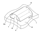
- FIG. 1 A perspective view which shows notionally an example of the formation method of the organic-semiconductor film of this invention.
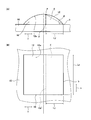
- FIG. 1 A perspective view of the formation method of the organic-semiconductor film shown in FIG. 1
- B is a top view of the formation method of the organic-semiconductor film shown in FIG.
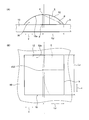
- A) is a front view of another example of the method for forming an organic semiconductor film of the present invention
- FIG. (B) is a plan view.
- A)-(I) is a figure which shows notionally another example of the formation method of the organic-semiconductor film of this invention. It is a conceptual diagram for demonstrating the formation method of the organic-semiconductor film of this invention.
- FIG. 1 and 2 conceptually show an example of a method for forming an organic semiconductor film of the present invention.
- 2A is a front view of FIG. 1 viewed from the direction of arrow x
- FIG. 2B is a plan view of FIG. 1 viewed from above.
- the method for forming an organic semiconductor film of the present invention forms an organic semiconductor film using a solution obtained by dissolving an organic semiconductor material to be an organic semiconductor film in a solvent.
- the organic semiconductor film forming method of the present invention includes a cover member 12 that forms a space 16 with a substrate 10 on a substrate 10 on which the organic semiconductor film is formed.
- the space 16 is filled with a solution obtained by dissolving an organic semiconductor material to be an organic semiconductor film in a solvent (hereinafter referred to as a coating solution E) so as to be in contact with the substrate 10 and the cover member 12.
- the coating liquid E is dried, and then the cover member 12 is removed to form an organic semiconductor film.
- the substrate 10 has an organic semiconductor film formed on the surface thereof. That is, the substrate 10 is a substrate of an organic semiconductor element.
- a plate-like material (sheet-like material / film) made of various materials such as metals such as silicon, ceramics, glass, and plastics. ) Is available.
- the substrate on which the organic semiconductor film is formed in addition to a simple plate-like material as shown in the drawing, materials having various configurations that can be used for manufacturing an organic semiconductor element can be used.
- the substrate may be one in which an insulating layer is formed on the entire surface or a part of the surface of the support (semiconductor element substrate).
- a gate electrode is formed on the support, and the support and the gate electrode are formed.
- An insulating layer may be formed so as to be covered, or an insulating layer may be formed on the surface of a support serving as a gate electrode, and a source electrode and a drain electrode may be formed thereon.
- the organic semiconductor film forming method of the present invention can be applied to various known organic semiconductor elements such as bottom gate-bottom contact type, top gate-bottom contact type, bottom gate-top contact type, top gate-bottom contact type. It can be used for forming an organic semiconductor film (organic semiconductor layer) in a manufacturing process.
- organic semiconductor film organic semiconductor layer
- various types exemplified by the above-described substrate 10 can be used as a support body of these substrates.
- the cover member 12 forms a space for filling the coating liquid E to be an organic semiconductor film with the surface of the substrate 10 on which the organic semiconductor film is formed (hereinafter also referred to as the surface) (that is, coating of the coating liquid E).
- the region is regulated), and the drying of the coating liquid E (solvent evaporation) is controlled.
- the cover member has an uppermost portion that is farthest from the surface of the substrate 10 and a descending portion that is provided on both sides of the uppermost portion in the direction of the arrow y and faces the surface of the substrate 10 from the uppermost portion.
- the control surface is disposed with the control surface facing the substrate 10. Further, the space formed by the restriction surface of the cover member together with the surface of the substrate 10 is open in the x direction orthogonal to the y direction.
- the cover member 12 has a shape formed by curving a square plate material (sheet-like material / film) into an arc shape (cylindrical circumferential surface shape).
- the concave surface of the circular arc becomes the regulating surface 12a.
- the cover member 12 is placed on the surface of the substrate 10 with the circumferential direction of the arc (the direction perpendicular to the center line) as the y direction and the concave surface that is the regulating surface 12a facing the substrate 10. Therefore, the x direction orthogonal to the y direction is parallel to the center line of this arc (in FIG. 2A, the x direction is perpendicular to the paper surface). Further, the cover member 12 is disposed so that the entire area at both ends in the y direction is in contact with the surface of the substrate 10.
- the position indicated by the alternate long and short dash line in FIG. 2 is the uppermost portion of the cover member 12 (the uppermost portion of the arc). Therefore, the regulation surface 12a of the cover member 12 has a configuration in which a descending portion that faces the surface of the substrate 10 in an arc shape from the uppermost portion indicated by the alternate long and short dash line toward both sides in the y direction.
- the base end is the end in the y direction where the entire region contacts the surface of the substrate 10, and the base end side is filled with the coating liquid E.
- both end portions in the y direction of the regulation surface 12 a are in contact with the substrate 10 over the entire surface.
- the cover member 12 may have any end portion in the y direction as a base end.
- the right side in the figure is the base end b.
- the base member b side of the space 16 formed by the cover member 12 and the substrate 10 is brought into contact with the cover member 12 and the substrate 10 and filled with the coating liquid E.
- the coating liquid E is dried to form an organic semiconductor film.
- the coating liquid E is viewed from the base end b, at least a part of the end portion in the y direction opposite to the base end b on the regulation surface 12a does not exceed the uppermost portion, that is, the alternate long and short dash line. , The space 16 is filled.
- the coating liquid E is a line in the y direction that connects the base end b and a position e where the coating liquid E is farthest from the base end b in the y direction on the regulation surface 12a (hereinafter also referred to as a separation position e).
- the apparent angle ⁇ which is an angle formed by a line in the y direction connecting the base p and the point p where the perpendicular line drawn from the separation position e to the substrate 10 intersects the substrate 10 and the base end b, is 50 ° or less.
- the space 16 is filled so as to be.
- the coating liquid E has a space such that the apex angle on the base end b side of the right triangle that forms a plane parallel to the y direction connecting the base end b, the separation position e, and the point p is 50 ° or less. 16 is filled. Further, the coating liquid E is filled in the space 16 so that the x / y ratio obtained by dividing the length Lx in the x direction by the length Ly in the y direction is 0.2 or more.
- the organic semiconductor film forming method of the present invention uses the cover member 12 having such a predetermined shape, and applies a coating solution in the space 16 formed by the substrate 10 and the cover member 12 so as to satisfy the above three conditions. E is filled, and the coating liquid E is dried to form an organic semiconductor film.
- the present invention increases the concentration of the solvent in the evaporation space of the coating liquid E, that is, the space 16 to reduce the evaporation rate of the solvent of the coating liquid E, that is, the drying speed.
- the drying speed of the coating liquid E can be suitably adjusted. Therefore, according to the method for forming an organic semiconductor film of the present invention, it is possible to appropriately control the drying of the coating liquid E, to obtain a high-quality organic semiconductor that has favorable crystallinity and crystal size and has a low defect frequency. Can be formed.
- the liquid surface of the coating liquid E filled in the space 16 is shown as a plane for the sake of simplicity of the drawings and description.
- the liquid level is not necessarily flat, and often has a convex shape or a concave shape.
- the liquid surface opposite to the base end b in the y direction may be convex.
- the liquid surface may be concave.
- a position that is the most distant from the base end b in the y direction is set as a separation position e.
- the coating liquid E is transferred to the base end on the regulation surface 12a. It is not necessary to be positioned closer to the base end b side than the uppermost portion of the regulation surface 12a when viewed from the b side. That is, in the present invention, as shown in FIG. 3, the coating liquid E is partly on the base end b side in the y direction with respect to the base end b, as viewed from the base end b. If located, there may be a region exceeding the uppermost portion in the y direction when viewed from the base end b.
- the restricting surface 12a of the cover member 12 extends in the y direction from the uppermost portion on the uppermost portion that is farthest from the substrate 10 and on both sides of the uppermost portion in the y direction. And a descending portion toward the surface. That is, the regulation surface 12a of the cover member 12 has a region that descends from the top to the substrate 10 on the other side of the top when viewed in the y direction from the base end b filled with the coating liquid E. .
- Such a regulating surface 12a of the cover member 12 forms, together with the substrate 10, a convex space 16 having the top as a vertex toward the top (the opposite side to the substrate 10). Therefore, the solvent evaporated from the coating liquid E stays in the convex space 16, and as a result, the solvent concentration in the space 16 can be increased and the drying speed of the coating liquid E can be reduced.
- the end surface in the x direction of the space 16 formed by the substrate 10 and the cover member 12 may be partially open, but it is preferable that the entire surface is open as in the illustrated example. Thereby, the controllability of drying of the coating liquid E can be further improved by the apparent angle ⁇ and the x / y ratio, and further by the contact area ratio with the outside air described later.
- the coating liquid E filling the space 16 is filled such that at least a part thereof does not exceed the uppermost portion when viewed from the base end b on the regulation surface 12a.
- the coating liquid E is opposite to the base end b in the y direction. Will flow to the end of the side. Therefore, the coating liquid E is applied to a position different from the base end b side of the space 16, that is, the place where the organic semiconductor film is formed, and the organic semiconductor film cannot be formed at the target position.
- a line connecting the base end b and the separation position e (two-dot chain line) and a line connecting the point p where the perpendicular line from the separation position e intersects the substrate 10 and the base end b are formed.
- the apparent angle ⁇ formed is an apparent angle at the base end b of the coating liquid E filling the space 16.
- the space 16 is filled with the coating liquid E so that the apparent angle ⁇ is 50 ° or less.
- the apparent angle ⁇ exceeds 50 °, the contact area of the coating liquid E with the outside air becomes too large, the drying speed of the coating liquid E becomes too fast, and the crystallinity of the organic semiconductor is lowered.
- the apparent angle is preferably 40 ° or less, more preferably 30 ° or less, and particularly preferably 20 ° or less.
- the apparent angle ⁇ only needs to exceed 0 °.
- the smaller the apparent angle ⁇ the slower the drying of the coating solution, so that the productivity is lowered and fine crystals are likely to be formed in the formed organic semiconductor film.
- the apparent angle ⁇ is preferably 3 ° or more, more preferably 5 ° or more, and particularly preferably 10 ° or more.
- the coating liquid E is filled in the space 16 so that the x / y ratio obtained by dividing the length Lx in the x direction of the coating liquid by the length Ly in the y direction is 0.2 or more. If the x / y ratio is less than 0.2, the contact area of the coating liquid E with the outside air becomes too large, the drying speed of the coating liquid E becomes too fast, and the crystallinity of the organic semiconductor decreases. Considering this point, the x / y ratio is preferably 0.2 or more, more preferably 0.3 or more, and particularly preferably 0.45 or more.
- the x / y ratio may be large considering the case where a large number of organic semiconductor elements are formed corresponding to the manufacture of TFTs (thin film transistors) for display.
- the x / y ratio is preferably 100,000 or less, more preferably 10,000 or less, further preferably 1000 or less, and particularly preferably 100 or less.
- the length Ly of the coating liquid E in the y direction is the position farthest from the base end b in the y direction on the substrate 10.
- the distance in the y direction between the base end b and the coating liquid E is defined as the length Ly of the coating liquid E in the y direction.
- the length Lx in the x direction of the coating liquid E is the distance in the x direction at the position where the liquid surface is most separated in the x direction on the substrate 10, and the length is the length Lx in the x direction.
- the surface area of the coating liquid E that is in contact with the outside air that is, the surface area of the coating liquid E that is not in contact with the substrate 10 and the cover member 12 is 35% or less of the entire surface area of the coating liquid E. It is preferably 32% or less, more preferably 30% or less, even more preferably 20% or less.
- the surface area of the coating liquid E in contact with the outside air is preferably 1% or more of the surface area of the coating liquid, more preferably 5% or more, more preferably 10% or more, and particularly preferably 15% or more is preferable.
- the liquid surface of the coating liquid E is not necessarily flat, and often has a concave or convex shape. Therefore, it is very difficult to accurately calculate the surface area of the coating liquid. is there. Therefore, in the present invention, the liquid surface opposite to the base end b in the y direction of the coating liquid E is regarded as a planar shape parallel to the x direction at a position where the base end b and the coating liquid E are most separated in the y direction. . Further, the liquid surface of the coating liquid E on both sides in the x direction is a plane parallel to the y direction connecting the base end b, the separation position e, and the point p using the liquid surface in the y direction set in this way. As a right triangle. In the present invention, the surface area of the apparent coating liquid E calculated using the liquid level set in this way is defined as the surface area of the coating liquid E.
- the cover member has a convex space as described above in addition to the arc shape in which both ends of the regulating surface 12a in the y direction are in contact with the substrate 10 as shown in the illustrated example. As long as it can be formed, various shapes can be used. Further, the cover member can be disposed on the substrate 10 in various states.
- the arc-shaped cover member may be configured such that one end in the y direction does not contact the substrate 10.
- the horizontal direction in the figure is the y direction.
- the side of the cover member that is not in contact with the substrate 10 may be supported by a columnar member. Or you may suspend and support the side which is not contacting the board
- the cover member is such that both ends in the y direction are in contact with the substrate 10 in that the solvent concentration in the evaporation space of the coating liquid E can be suitably increased and the evaporation of the coating liquid E can be easily controlled.
- it is more preferable that the entire area at both ends in the y direction is in contact with the substrate 10.
- one end portion in the y direction contacts the entire substrate 10 and the other end portion. May be configured such that a part thereof does not contact the substrate 10 but partially contacts the substrate 10.
- one end in the y direction contacts the entire substrate 10 and the other one
- the end may have a rectangular notch, and the end other than the notch may be in contact with the substrate 10.
- the cutout may have various shapes such as a triangle and a circle in addition to the rectangle. Further, the notch may be formed not at the center in the x direction but at the end.
- the cover member may have a trapezoidal shape as conceptually shown in FIGS. 4 (E) and (F). Since the cover member has regions parallel to both ends in the y direction, such as the square shown in FIG. 1, the trapezoid, or the rectangle, both ends in the y direction of the cover member can be easily brought into contact with the substrate 10. Preferably, the entire area at both ends in the y direction can contact the substrate 10.
- the cover member does not have to have a shape having a descending portion that gradually approaches the substrate 10 on both sides in the y direction from the uppermost portion as in the above example.
- the cover member having a shape in which the end portion of the rectangular parallelepiped is bent at a right angle (ie, a cube shape in which one side of the maximum surface and two opposite side surfaces are opened) is bent.
- the configuration may be such that the bent end is in contact with the substrate 10 with the side as the y direction.
- the uppermost portion is planar, and the portion bent at a right angle is the descending portion.
- the upper surface may be inclined in a triangular shape as conceptually shown in FIG. 4 (H), not in a planar shape as shown in FIG. 4 (G), and further in FIG. 4 (I). As shown specifically, it may be configured to have a portion inclined toward the substrate 10 on one side of the descending portion.
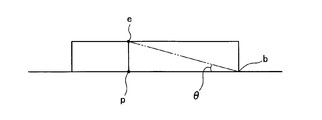
- the apparent angle ⁇ described above is used.
- the line connecting the base end b and the separation position e farthest from the base end b in the y direction on the regulation surface and the perpendicular from the separation position e are the substrate.
- An angle formed by a point p intersecting 10 and a line connecting the base end b is defined as an apparent angle ⁇ .
- the cover member is not limited to the plate-like object as shown in the illustrated example, and various kinds of materials can be used as long as the restriction surface forming the convex space as described above is formed.
- a member of the shape can be used.
- a concave portion such as an arc column is formed on one surface of a block-shaped member such as a cube or a rectangular parallelepiped, and a space for filling a solution with the substrate 10 is formed using this surface as a regulating surface.
- the number of cover members disposed on the surface of the substrate 10 is not limited to one, and a plurality of cover members are disposed on the surface of one substrate to form an organic semiconductor film. Also good.
- one cover member may have a plurality of regulating surfaces corresponding to the formation of a plurality of organic semiconductor films.
- the cover member 12 can be formed of various materials. Specifically, polytetrafluoroethylene, polychlorotrifluoroethylene (trifluorinated resin, polyvinylidene fluoride, polyvinyl fluoride, fluorinated resin copolymer, perfluoroalkoxy fluororesin, tetrafluoroethylene / hexafluoropropylene
- a liquid-repellent material such as a copolymer, a fluororesin such as an ethylene / tetrafluoroethylene copolymer or an ethylene / chlorotrifluoroethylene copolymer, or a silicone resin is preferred.
- a material such as a resin coated with a liquid repellent resin or a liquid repellent treatment is preferably used as the cover member 12.
- the size of the cover member 12 may be appropriately determined according to the organic semiconductor film to be formed.
- the cover member 12 is disposed on the surface of the substrate 10, and the organic semiconductor film is formed on the base end b side of the space 16 formed by the surface of the substrate 10 and the cover member 12.
- An organic semiconductor film is formed on the surface of the substrate 10 by filling the coating liquid E obtained by dissolving the organic semiconductor material, drying the coating liquid E, and then removing the cover member 12.
- the cover member 12 before the cover member 12 is arrange
- Various surface treatments such as treatment may be performed.
- the organic semiconductor material various known materials that can be used for an organic semiconductor film formed by a so-called wet process (wet process) such as a coating method in the manufacture of an organic semiconductor element can be used.
- wet process such as a coating method in the manufacture of an organic semiconductor element
- Specific examples include pentacenes such as 6,13-bis (triisopropylsilylethynyl) pentacene (TIPS pentacene), rubrenes, fullerenes, phthalocyanines, TCNQs, and the like.
- TIPS pentacene 6,13-bis (triisopropylsilylethynyl) pentacene
- rubrenes fullerenes
- phthalocyanines phthalocyanines
- TCNQs phthalocyanines
- solvents can be used as the solvent contained in the coating liquid E as long as it can dissolve the organic semiconductor material to be used.
- the organic semiconductor material is an acene such as TIPS pentacene, toluene, anisole, n-butylbenzene, acetone and the like are preferably exemplified.
- the concentration of the organic semiconductor material in the coating liquid E may be set as appropriate according to the type of organic semiconductor material, the type of solvent, the thickness of the organic semiconductor film to be formed, the shape of the cover member 12, and the like.
- the coating liquid E may contain a surfactant, a polymer, or the like, if necessary, in addition to the organic semiconductor material and the solvent.
- the coating liquid E contains components other than such an organic semiconductor material and a solvent, it is preferable that the content shall be 50 mass% or less.
- Example 1 An n-type silicon substrate having a size of 20 ⁇ 20 mm and a thickness of 0.5 mm was prepared. The surface of this silicon substrate was heat-treated to form a thermal oxide film having a thickness of 300 nm. Furthermore, the surface of the thermal oxide film was irradiated with UV light to improve paintability.
- Teflon plate having a size of 16 ⁇ 16 mm and a thickness of 0.2 mm was prepared.
- This Teflon plate was curved in one direction to form an arc-shaped (cylindrical circumferential surface) cover member 12 having a height of 1 mm as shown in FIGS.
- TIPS pentacene was dissolved in toluene to prepare a coating solution E.
- the concentration of TIPS pentacene in the coating solution was 1% by mass.
- the cover member 12 was placed on the substrate 10. Since the cover member 12 has an arc shape with a height of 1 mm, the height of the uppermost portion of the cover member 12 is 1 mm.
- the coating liquid E was filled on the base end b side of the space 16 using a dropper. In the filling of the coating liquid E, the position in the y direction that is farthest from the base end b on the regulating surface 12a of the cover member 12 coincides with the uppermost portion, and the x direction reaches the entire area of the cover member 12. went. Therefore, in this example, the coating liquid E has a length Ly in the y direction of 8 mm and a length Lx in the x direction of 16 mm.
- the substrate 10 and the cover member 12 filled with the coating liquid E in this way were dried for 10 minutes in a draft chamber. After drying, the substrate 10 was taken out from the draft chamber, the cover member 12 was removed, and the substrate 10 having an organic semiconductor thin film formed on the surface was produced.
- organic semiconductor film TIPS pentacene film
- two gold electrodes having a square pattern with a side of 1 mm are formed at 50 ⁇ m intervals by vacuum deposition, and an organic semiconductor element (organic thin film transistor) is formed.
- an organic semiconductor element organic thin film transistor
- the silicon wafer is a gate electrode
- the thermal oxide film is a gate insulating film
- the two gold electrodes are a source electrode and a drain electrode, respectively.
- Example 2 to [Example 9] Except for the height of the arc of the cover member 12 being 1.6 mm (Example 2), Except that the length in the x direction of the Teflon plate to be the cover member 12 is 8 mm (Example 3), Example 4 except that the length in the x direction of the Teflon plate to be the cover member 12 was 4 mm, (Example 5) except that the length in the y direction of the Teflon plate to be the cover member 12 was 32 mm (that is, the length Ly of the coating liquid was 16 mm).
- Example 9 An organic semiconductor element was produced by forming an organic semiconductor film in the same manner as in Example 1 except that the length in the x direction of the Teflon plate serving as the cover member 12 was 160 mm (Example 9). In the example in which the Teflon plate serving as the cover member 12 is larger than the substrate 10, a large n-type silicon substrate was used, and the cover member 12 was placed in the center.
- the field effect transistor was evaluated by connecting each electrode of each organic semiconductor element thus produced and each terminal of a manual prober connected to Agilent Technologies 4155C. Specifically, the field effect mobility ([cm 2 / V ⁇ sec]) was calculated by measuring the drain current-gate voltage (Id-Vg) characteristics.
- Example 1 was 1 ⁇ 10 ⁇ 1 ;
- Example 2 was 1.5 ⁇ 10 ⁇ 1 ;
- Example 3 was 8 ⁇ 10 ⁇ 2 ;
- Example 4 was 5 ⁇ 10 ⁇ 2 ;
- Example 5 was 1 .5 ⁇ 10 -1; example 6 7 ⁇ 10 -2; example 7 4 ⁇ 10 -2; example 8 1.5 ⁇ 10 -1; example 9 2 ⁇ 10 -1; in there were.
- Comparative Example 1 was 5 ⁇ 10 ⁇ 3 ; Comparative Example 2 was 5 ⁇ 10 ⁇ 3 ; Comparative Example 3 was; 1 ⁇ 10 ⁇ 3 ; Comparative Example 4 was 5 ⁇ 10 ⁇ 3 ;
- the results are also shown in the table below.
- Comparative Example 4 that does not have a descending portion directed from the top to the opposite side of the base end, the solvent evaporated from the coating liquid E is discharged to the outside of the cover member, and the solvent concentration inside the cover member cannot be increased. Similarly, the drying of the coating liquid E cannot be controlled, and high mobility is not obtained. From the above results, the effects of the present invention are clear.
Landscapes
- Engineering & Computer Science (AREA)
- Manufacturing & Machinery (AREA)
- Liquid Deposition Of Substances Of Which Semiconductor Devices Are Composed (AREA)
- Thin Film Transistor (AREA)
- Electroluminescent Light Sources (AREA)
Abstract
本発明は、良好な結晶性を有し、移動度が高い有機半導体膜を、安定して形成できる有機半導体膜の形成方法を提供することを目的とする。本発明は、有機半導体膜の形成において、基板表面の有機半導体膜の形成位置の上部を、一方向に基板から離間する凸の空間を形成する規制面を有するカバー部材で覆って、カバー部材と基板との間に、所定の条件を満たすように溶液を充填して、この溶液を乾燥することで有機半導体膜を形成するものである。これにより、有機半導体材料を溶解した溶液を用いて、良好な結晶性を有する有機半導体膜を形成するものである。
Description
本発明は、有機半導体材料を用いた薄膜トランジスタなどに用いられる有機半導体膜の形成方法に関する。
軽量化、低コスト化、柔軟化が可能であることから、液晶ディスプレイや有機ELディスプレイに用いられるTFT(薄膜トランジスタ)、RFID(RFタグ)やメモリなどの論理回路を用いる装置等に、有機半導体材料からなる有機半導体膜(有機半導体層)を有する有機半導体素子が利用されている。
有機半導体素子の製造において、有機半導体膜の形成方法の1つとして、有機半導体材料を溶剤に溶解した塗料を基板に塗布し、溶液を乾燥させることで有機半導体膜を形成する、湿式の方法が知られている。
この湿式の有機半導体膜の形成方法は、安価に有機半導体膜が形成できる、大面積に対応して有機半導体膜が形成できる等、各種の利点を有する。
この湿式の有機半導体膜の形成方法は、安価に有機半導体膜が形成できる、大面積に対応して有機半導体膜が形成できる等、各種の利点を有する。
ところで、移動度の高い有機半導体膜を得るためには、有機半導体膜の結晶性を向上することが重要である。そのため、このような湿式の有機半導体膜の形成においても、有機半導体膜の結晶性を向上する方法が、各種、提案されている。
例えば、特許文献1には、基板上の有機半導体膜の形成位置を囲むように枠体を形成し、この枠体の中に有機半導体材料を溶解した溶液を充填し、この溶液を乾燥することによって、有機半導体の結晶を形成する方法が記載されている。
また、特許文献2には、有機半導体材料を溶解した溶液を付着させる接触面を有する接触部材を用い、基板の表面に対して、この接触面が一定の関係となるように接触部材を配置し、溶液を接触部材の接触面に保持させて、乾燥することにより、結晶性の有機半導体膜を形成する方法が記載されている。
具体的には、基板に垂直に立設する接触面を有する接触部材を用い、接触面と基板とが成す角部に溶液を充填して、乾燥することにより、結晶性の有機半導体膜を形成する方法が記載されている。また、別の方法として、基板に対して傾斜する接触面を有する接触部材を用い、接触面と基板とを、所定の間隔、離間して配置し、接触面と基板との間に、両者に接触して溶液を充填して、乾燥することにより、結晶性の有機半導体膜を形成する方法も記載されている。
具体的には、基板に垂直に立設する接触面を有する接触部材を用い、接触面と基板とが成す角部に溶液を充填して、乾燥することにより、結晶性の有機半導体膜を形成する方法が記載されている。また、別の方法として、基板に対して傾斜する接触面を有する接触部材を用い、接触面と基板とを、所定の間隔、離間して配置し、接触面と基板との間に、両者に接触して溶液を充填して、乾燥することにより、結晶性の有機半導体膜を形成する方法も記載されている。
これらの方法によれば、結晶性を有する有機半導体膜を形成できる。
しかしながら、近年の有機半導体膜の形成に対する要求は、さらに厳しくなっており、より良好な結晶性を有し、高い移動度の半導体素子が得られる有機半導体膜を、安定して形成できる方法の出現が望まれている。
しかしながら、近年の有機半導体膜の形成に対する要求は、さらに厳しくなっており、より良好な結晶性を有し、高い移動度の半導体素子が得られる有機半導体膜を、安定して形成できる方法の出現が望まれている。
本発明の目的は、このような従来技術の問題点を解決することにあり、良好な結晶性を有し、移動度が高い有機半導体膜を、安定して形成できる有機半導体膜の形成方法を提供することにある。
このような目的と達成するために、本発明の有機半導体膜の形成方法は、有機半導体材料を溶解した溶液を用いて、有機半導体材料からなる有機半導体膜を形成するに際し、
有機半導体膜を形成する基板の上に配置される、基板との間で空間を形成するカバー部材を用い、カバー部材と基板との間の空間に溶液を充填して、充填した溶液を乾燥することにより、有機半導体膜を形成するものであり、
カバー部材は、基板から最も離間する最上部と、最上部から基板に向かう、最上部のy方向の両側に設けられる降下部とが形成された規制面を有し、かつ、規制面が形成する空間のy方向と直交するx方向は開放する形状であり、規制面を基板に向けて、y方向の少なくとも一方の端部の全域を基板に接触した状態で配置され、
また、カバー部材の全域を基板に接触するy方向の端部を基端とした際に、規制面上における基端と逆側のy方向の端部の溶液の少なくとも一部が、基端から見た際に規制面の最上部を超えない場所に位置し、かつ、基端、および、規制面上においてy方向に溶液が基端と最も離間する位置である離間位置を結ぶ最短の線と、離間位置から基板に下ろした垂線が基板に交差する点、および、基端を結ぶ最短の線とが成す角度である見掛け角度が50°以下となり、さらに、x方向の長さを、y方向の長さで除したx/y比が0.2以上となるように、カバー部材と基板との間の空間の基端側に溶液を充填することを特徴とする有機半導体膜の形成方法を提供する。
有機半導体膜を形成する基板の上に配置される、基板との間で空間を形成するカバー部材を用い、カバー部材と基板との間の空間に溶液を充填して、充填した溶液を乾燥することにより、有機半導体膜を形成するものであり、
カバー部材は、基板から最も離間する最上部と、最上部から基板に向かう、最上部のy方向の両側に設けられる降下部とが形成された規制面を有し、かつ、規制面が形成する空間のy方向と直交するx方向は開放する形状であり、規制面を基板に向けて、y方向の少なくとも一方の端部の全域を基板に接触した状態で配置され、
また、カバー部材の全域を基板に接触するy方向の端部を基端とした際に、規制面上における基端と逆側のy方向の端部の溶液の少なくとも一部が、基端から見た際に規制面の最上部を超えない場所に位置し、かつ、基端、および、規制面上においてy方向に溶液が基端と最も離間する位置である離間位置を結ぶ最短の線と、離間位置から基板に下ろした垂線が基板に交差する点、および、基端を結ぶ最短の線とが成す角度である見掛け角度が50°以下となり、さらに、x方向の長さを、y方向の長さで除したx/y比が0.2以上となるように、カバー部材と基板との間の空間の基端側に溶液を充填することを特徴とする有機半導体膜の形成方法を提供する。
このような本発明の有機半導体膜の形成方法において、溶液の記基板およびカバー部材に接触していない部分の表面積が、溶液全体の表面積の35%以下であるのが好ましい。
また、溶液の基板およびカバー部材に接触していない部分の表面積が、溶液全体の表面積の1%以上であるのが好ましい。
また、見掛け角度が3°以上であるのが好ましい。
また、x/y比が100000以下であるのが好ましい。
また、カバー部材を、y方向の両端部を基板に接触して配置するのが好ましい。
また、カバー部材を、y方向の両端部の全域を基板に接触して配置するのが好ましい。
また、カバー部材が板状であるのが好ましい。
さらに、カバー部材が、y方向の両端部に平行な領域を有するのが好ましい。
また、溶液の基板およびカバー部材に接触していない部分の表面積が、溶液全体の表面積の1%以上であるのが好ましい。
また、見掛け角度が3°以上であるのが好ましい。
また、x/y比が100000以下であるのが好ましい。
また、カバー部材を、y方向の両端部を基板に接触して配置するのが好ましい。
また、カバー部材を、y方向の両端部の全域を基板に接触して配置するのが好ましい。
また、カバー部材が板状であるのが好ましい。
さらに、カバー部材が、y方向の両端部に平行な領域を有するのが好ましい。
このような本発明によれば、有機半導体材料を溶解した溶液を用いる有機半導体膜の形成において、溶剤の蒸発を適正に制御して、結晶性の良好な有機半導体膜を、安定して形成することができる。
図1および図2に、本発明の有機半導体膜の形成方法の一例を概念的に示す。
なお、図2において、(A)は、図1を矢印x方向から見た正面図で、(B)は、図1を上方から見た平面図である。
なお、図2において、(A)は、図1を矢印x方向から見た正面図で、(B)は、図1を上方から見た平面図である。
本発明の有機半導体膜の形成方法(以下、単に『本発明の形成方法』とも言う)は、有機半導体膜となる有機半導体材料を溶剤に溶解してなる溶液を用いて、有機半導体膜を形成するものである。
図1および図2に概念的に示すように、本発明の有機半導体膜の形成方法は、有機半導体膜を形成する基板10の上に、基板10との間で空間16を形成するカバー部材12を配置し、この空間16に、基板10およびカバー部材12に接触するように、有機半導体膜となる有機半導体材料を溶剤に溶解してなる溶液(以下、塗布液Eとする)を充填し、この塗布液Eを乾燥して、その後、カバー部材12を取り外すことにより、有機半導体膜を形成する。
図1および図2に概念的に示すように、本発明の有機半導体膜の形成方法は、有機半導体膜を形成する基板10の上に、基板10との間で空間16を形成するカバー部材12を配置し、この空間16に、基板10およびカバー部材12に接触するように、有機半導体膜となる有機半導体材料を溶剤に溶解してなる溶液(以下、塗布液Eとする)を充填し、この塗布液Eを乾燥して、その後、カバー部材12を取り外すことにより、有機半導体膜を形成する。
本発明の形成方法において、基板10は、その表面に有機半導体膜を形成されるものである。すなわち、基板10は、有機半導体素子の基板等となる。
基板10としては、有機半導体材料を溶解した有機半導体膜の形成が可能なものであれば、シリコン等の金属、セラミック、ガラス、プラスチックなど、各種の材料からなる板状物(シート状物/フィルム)が利用可能である。
また、有機半導体膜を形成する基板は、図示例のような単純な板状物以外にも、有機半導体素子の製造おける、各種の構成の物が利用可能である。
一例として、基板は、支持体(半導体素子の基板)の表面の全面あるいは一部に絶縁層が形成された物でもよく、支持体の上にゲート電極を形成して、支持体およびゲート電極を覆って絶縁層を形成した物でもよく、ゲート電極となる支持体の表面に絶縁層を形成して、その上にソース電極およびドレイン電極を形成した物でもよい。
すなわち、本発明の有機半導体膜の形成方法は、ボトムゲート-ボトムコンタクト型、トップゲート-ボトムコンタクト型、ボトムゲート-トップコンタクト型、トップゲート-ボトムコンタクト型など、公知の各種の有機半導体素子の製造工程における、有機半導体膜(有機半導体層)の形成に利用可能である。
なお、これらの基板の支持体としては、前述の基板10で例示したものが、各種、利用可能である。
一例として、基板は、支持体(半導体素子の基板)の表面の全面あるいは一部に絶縁層が形成された物でもよく、支持体の上にゲート電極を形成して、支持体およびゲート電極を覆って絶縁層を形成した物でもよく、ゲート電極となる支持体の表面に絶縁層を形成して、その上にソース電極およびドレイン電極を形成した物でもよい。
すなわち、本発明の有機半導体膜の形成方法は、ボトムゲート-ボトムコンタクト型、トップゲート-ボトムコンタクト型、ボトムゲート-トップコンタクト型、トップゲート-ボトムコンタクト型など、公知の各種の有機半導体素子の製造工程における、有機半導体膜(有機半導体層)の形成に利用可能である。
なお、これらの基板の支持体としては、前述の基板10で例示したものが、各種、利用可能である。
カバー部材12は、基板10の有機半導体膜の形成面(以下、表面とも言う)との間で、有機半導体膜となる塗布液Eを充填するための空間を形成(すなわち、塗布液Eの塗布領域を規制)し、さらに、塗布液Eの乾燥(溶剤の蒸発)を制御するものである。
本発明の形成方法において、カバー部材は、基板10の表面と最も離間する最上部と、この最上部の矢印y方向の両側に設けられる、最上部から基板10の表面に向かう降下部とを有する、規制面を有し、この規制面を基板10に向けて、配置される。また、カバー部材の規制面が基板10の表面と共に形成する空間は、y方向と直交するx方向が開放している。
本発明の形成方法において、カバー部材は、基板10の表面と最も離間する最上部と、この最上部の矢印y方向の両側に設けられる、最上部から基板10の表面に向かう降下部とを有する、規制面を有し、この規制面を基板10に向けて、配置される。また、カバー部材の規制面が基板10の表面と共に形成する空間は、y方向と直交するx方向が開放している。
図1および図2に示す例において、カバー部材12は、正方形の板材(シート状物/フィルム)を、円弧状(円筒の周面状)に湾曲させてなる形状を有する。
このカバー部材12においては、円弧の凹面が規制面12aとなる。カバー部材12は、円弧の周方向(中心線と直交する方向)をy方向として、規制面12aである凹面を基板10に向けて、基板10の表面に載置される。従って、y方向と直交するx方向は、この円弧の中心線と平行になる(図2(A)では、x方向は紙面に垂直方向)。
また、このカバー部材12は、y方向の両端の全域を基板10の表面に接触して配置される。
このカバー部材12においては、円弧の凹面が規制面12aとなる。カバー部材12は、円弧の周方向(中心線と直交する方向)をy方向として、規制面12aである凹面を基板10に向けて、基板10の表面に載置される。従って、y方向と直交するx方向は、この円弧の中心線と平行になる(図2(A)では、x方向は紙面に垂直方向)。
また、このカバー部材12は、y方向の両端の全域を基板10の表面に接触して配置される。
図示例においては、図2に一点鎖線で示す位置が、カバー部材12の最上部(円弧の最上部)である。
従って、カバー部材12の規制面12aは、一点鎖線で示す最上部からy方向の両側に向けて、円弧状に基板10の表面に向かう降下部を有する構成となる。
従って、カバー部材12の規制面12aは、一点鎖線で示す最上部からy方向の両側に向けて、円弧状に基板10の表面に向かう降下部を有する構成となる。
本発明の形成方法においては、全域が基板10の表面に接触するy方向の端部を、基端として、この基端側に塗布液Eを充填する。
前述のように、図示例のカバー部材12は、規制面12aのy方向の両端部が、全面を基板10に接触している。従って、このカバー部材12は、y方向のいずれの端部を基端としてもよい。図示例においては、一例として、図中、右側を基端bとする。
前述のように、図示例のカバー部材12は、規制面12aのy方向の両端部が、全面を基板10に接触している。従って、このカバー部材12は、y方向のいずれの端部を基端としてもよい。図示例においては、一例として、図中、右側を基端bとする。
本発明の形成方法においては、このようなカバー部材12と基板10とで形成される空間16の基端b側に、カバー部材12と基板10とに接触して、塗布液Eを充填して、この塗布液Eを乾燥することにより、有機半導体膜を形成する。
ここで、塗布液Eは、基端bから見た際に、規制面12a上における基端bと逆側のy方向の端部の少なくとも一部が、最上部すなわち一点鎖線を超えないように、空間16に充填される。
また、塗布液Eは、基端bと、規制面12a上においてy方向に塗布液Eが基端bと最も離間する位置e(以下、離間位置eとも言う)とを結ぶy方向の線(二点鎖線)、および、離間位置eから基板10に下ろした垂線が基板10と交差する点pと、基端bとを結ぶy方向の線が成す角度である見掛け角度θが50°以下となるように、空間16に充填される。言い換えれば、塗布液Eは、基端b、離間位置eおよび点pを結ぶ、y方向と平行な平面となる直角三角形の基端b側の頂角が、50°以下となるように、空間16に充填される。
さらに、塗布液Eは、x方向の長さLxを、y方向の長さLyで除したx/y比が0.2以上となるように、空間16に充填される。
ここで、塗布液Eは、基端bから見た際に、規制面12a上における基端bと逆側のy方向の端部の少なくとも一部が、最上部すなわち一点鎖線を超えないように、空間16に充填される。
また、塗布液Eは、基端bと、規制面12a上においてy方向に塗布液Eが基端bと最も離間する位置e(以下、離間位置eとも言う)とを結ぶy方向の線(二点鎖線)、および、離間位置eから基板10に下ろした垂線が基板10と交差する点pと、基端bとを結ぶy方向の線が成す角度である見掛け角度θが50°以下となるように、空間16に充填される。言い換えれば、塗布液Eは、基端b、離間位置eおよび点pを結ぶ、y方向と平行な平面となる直角三角形の基端b側の頂角が、50°以下となるように、空間16に充填される。
さらに、塗布液Eは、x方向の長さLxを、y方向の長さLyで除したx/y比が0.2以上となるように、空間16に充填される。
本発明の有機半導体膜の形成方法は、このような所定形状を有するカバー部材12を用い、かつ、上記3つの条件を満たすように、基板10とカバー部材12とで形成する空間16に塗布液Eを充填して、塗布液Eを乾燥して、有機半導体膜を形成する。
本発明は、このような構成を有することにより、塗布液Eの蒸発空間すなわち空間16における溶剤濃度を高くして、塗布液Eの溶剤の蒸発速度すなわち乾燥速度を遅くすると共に、塗布液Eと外気との接触面積(すなわち溶剤の蒸発面積)を制御して、塗布液Eの乾燥速度を好適に調節できる。
そのため、本発明の有機半導体膜の形成方法によれば、塗布液Eの乾燥を適正に制御して、結晶性および結晶のサイズが好適で、かつ、欠陥頻度が少ない、高品質な有機半導体を形成できる。
本発明は、このような構成を有することにより、塗布液Eの蒸発空間すなわち空間16における溶剤濃度を高くして、塗布液Eの溶剤の蒸発速度すなわち乾燥速度を遅くすると共に、塗布液Eと外気との接触面積(すなわち溶剤の蒸発面積)を制御して、塗布液Eの乾燥速度を好適に調節できる。
そのため、本発明の有機半導体膜の形成方法によれば、塗布液Eの乾燥を適正に制御して、結晶性および結晶のサイズが好適で、かつ、欠陥頻度が少ない、高品質な有機半導体を形成できる。
なお、図1および図2においては、図面および説明を簡潔にするため、空間16に充填される塗布液Eの液面を平面状に示しているが、空間16に充填される塗布液Eの液面は、必ずしも、平面状にはならず、凸面状や凹面状などの形状になる場合も多い。例えば、図3(A)および(B)に概念的に示すように、y方向の基端bと逆側の液面が、凸状になる場合もある。あるいは、逆に、この液面が凹状になる場合も有る。
この場合には、図3に示すように、規制面12a上の基端bと逆側の液面において、y方向に基端bと最も離間する位置を、離間位置eとする。
この場合には、図3に示すように、規制面12a上の基端bと逆側の液面において、y方向に基端bと最も離間する位置を、離間位置eとする。
また、図3に示すように、y方向の基端bと逆側の液面が凸状などの平面状ではない場合などには、規制面12a上において、全ての塗布液Eが、基端b側から見て規制面12aの最上部よりも基端b側に位置する必要はない。
すなわち、本発明において、塗布液Eは、図3に示すように、規制面12a上において、一部が、基端bから見て最上部(一点鎖線)よりもy方向の基端b側に位置していれば、基端bからみてy方向に最上部を超える領域が存在してもよい。
すなわち、本発明において、塗布液Eは、図3に示すように、規制面12a上において、一部が、基端bから見て最上部(一点鎖線)よりもy方向の基端b側に位置していれば、基端bからみてy方向に最上部を超える領域が存在してもよい。
前述のように、カバー部材12の規制面12aは、基板10から最も離間する最上部と、この最上部のy方向の両側に、最上部からy方向に延在して、最上部から基板10の表面に向かう降下部とを有する。すなわち、カバー部材12の規制面12aは、塗布液Eが充填される基端bからy方向に見た際に、最上部の向こう側に、最上部から基板10に向かって降下する領域を有する。
このようなカバー部材12の規制面12aは、基板10と共に、上(基板10と逆側)に向かって、最上部を頂点とする凸状の空間16を形成する。そのため、塗布液Eから蒸発した溶剤は、この凸状の空間16内に留まり、その結果、空間16内における溶剤濃度を高くして、塗布液Eの乾燥速度を低減できる。
このようなカバー部材12の規制面12aは、基板10と共に、上(基板10と逆側)に向かって、最上部を頂点とする凸状の空間16を形成する。そのため、塗布液Eから蒸発した溶剤は、この凸状の空間16内に留まり、その結果、空間16内における溶剤濃度を高くして、塗布液Eの乾燥速度を低減できる。
なお、基板10とカバー部材12とで形成する空間16のx方向の端面は、一部が開放していればよいが、図示例のように、全面が開放しているのが好ましい。
これにより、見掛け角度θやx/y比、さらには、後述する外気との接触面積割合による、塗布液Eの乾燥の制御性を、より向上できる。
これにより、見掛け角度θやx/y比、さらには、後述する外気との接触面積割合による、塗布液Eの乾燥の制御性を、より向上できる。
本発明の形成方法において、空間16に充填される塗布液Eが、少なくとも一部が、規制面12a上において、基端bから見て最上部を超えないように充填される。
空間16に充填される塗布液Eが、全て、規制面12a上において、基端bから見て最上部を超えるように充填されると、塗布液Eが、y方向の基端bとは逆側の端部に流れてしまう。そのため、空間16の基端b側すなわち有機半導体膜を形成する場所とは、異なる位置に塗布液Eが塗布されて、目的とする位置に有機半導体膜を形成できない。
空間16に充填される塗布液Eが、全て、規制面12a上において、基端bから見て最上部を超えるように充填されると、塗布液Eが、y方向の基端bとは逆側の端部に流れてしまう。そのため、空間16の基端b側すなわち有機半導体膜を形成する場所とは、異なる位置に塗布液Eが塗布されて、目的とする位置に有機半導体膜を形成できない。
また、本発明の形成方法において、基端bおよび離間位置eを結ぶ線(二点鎖線)と、離間位置eからの垂線と基板10とが交差する点pおよび基端bを結ぶ線とが成す見掛け角度θとは、すなわち、空間16に充填される塗布液Eの、基端bにおける見かけ上の角度である。
本発明においては、この見掛け角度θは50°以下となるように、空間16に塗布液Eを充填する。見掛け角度θが50°を超えると、塗布液Eの外気との接触面積が大きく成り過ぎて、塗布液Eの乾燥速度が早くなり過ぎてしまい、有機半導体の結晶性が低下していまう。
この点を考慮すると、見掛け角度は、40°以下が好ましく、30°以下が、より好ましく、特に、20°以下が好ましい。
本発明においては、この見掛け角度θは50°以下となるように、空間16に塗布液Eを充填する。見掛け角度θが50°を超えると、塗布液Eの外気との接触面積が大きく成り過ぎて、塗布液Eの乾燥速度が早くなり過ぎてしまい、有機半導体の結晶性が低下していまう。
この点を考慮すると、見掛け角度は、40°以下が好ましく、30°以下が、より好ましく、特に、20°以下が好ましい。
他方、見掛け角度θは、0°を超えればよい。しかしながら、見掛け角度θは、小さくなるほど、塗布液の乾燥が遅くなるため、生産性が低下し、また、形成された有機半導体膜に、細かい結晶が生じ易い。
この点を考慮すると、見掛け角度θは、3°以上が好ましく、5°以上が、より好ましく、特に、10°以上が好ましい。
この点を考慮すると、見掛け角度θは、3°以上が好ましく、5°以上が、より好ましく、特に、10°以上が好ましい。
本発明においては、塗布液のx方向の長さLxを、y方向の長さLyで除したx/y比が0.2以上となるように、塗布液Eを空間16に充填する。
x/y比が0.2未満では、塗布液Eの外気との接触面積が大きく成り過ぎて、塗布液Eの乾燥速度が早くなり過ぎてしまい、有機半導体の結晶性が低下してしまう。
この点を考慮すると、x/y比は、0.2以上が好ましく、0.3以上が、より好ましく、特に、0.45以上が好ましい。
x/y比が0.2未満では、塗布液Eの外気との接触面積が大きく成り過ぎて、塗布液Eの乾燥速度が早くなり過ぎてしまい、有機半導体の結晶性が低下してしまう。
この点を考慮すると、x/y比は、0.2以上が好ましく、0.3以上が、より好ましく、特に、0.45以上が好ましい。
他方、ディスプレイ用のTFT(薄膜トランジスタ)の製造などに対応して、多数の有機半導体素子を形成する場合を考慮すると、x/y比は、大きくてもよい。
しかしながら、本発明者の検討によれば、x/y比は、100000以下が好ましく、10000以下が、より好ましく、1000以下が、さらに好ましく、特に、100以下が好ましい。
しかしながら、本発明者の検討によれば、x/y比は、100000以下が好ましく、10000以下が、より好ましく、1000以下が、さらに好ましく、特に、100以下が好ましい。
なお、前述のように、塗布液Eの液面が、平面ではない場合には、y方向の塗布液Eの長さLyは、基板10上において、y方向に最も基端bと離間する位置における、基端bと塗布液Eとのy方向の距離を、y方向の塗布液Eの長さLyとする。
また、塗布液Eのx方向の長さLxは、基板10上において、x方向に液面が最も離間する位置のx方向の距離を、長さを、x方向の長さLxとする。
また、塗布液Eのx方向の長さLxは、基板10上において、x方向に液面が最も離間する位置のx方向の距離を、長さを、x方向の長さLxとする。
本発明の有機半導体膜の形成方法においては、塗布液Eが外気と接触している面積が大き過ぎると、塗布液Eの乾燥速度が早くなり過ぎてしまい、有機半導体の結晶性が低下してしまう可能性が有る。
この点を考慮すると、塗布液Eの外気に接触している表面積、すなわち、塗布液Eの基板10およびカバー部材12に接触していない表面積は、塗布液E全体の表面積の35%以下であるのが好ましく、32%以下が、より好ましく、30%以下が、さらに好ましく、特に、20%以下が好ましい。
この点を考慮すると、塗布液Eの外気に接触している表面積、すなわち、塗布液Eの基板10およびカバー部材12に接触していない表面積は、塗布液E全体の表面積の35%以下であるのが好ましく、32%以下が、より好ましく、30%以下が、さらに好ましく、特に、20%以下が好ましい。
逆に、本発明の形成方法において、塗布液Eの外気に接触している面積が小さくなるほど、塗布液の乾燥が遅くなるため、生産性が低下し、また、形成された有機半導体膜に、細かい結晶が生じ易い。
この点を考慮すると、塗布液Eの外気に接触している表面積は、塗布液の表面積の1%以上であるのが好ましく、5%以上が、より好ましく、10%以上が、さらに好ましく、特に、15%以上が好ましい。
この点を考慮すると、塗布液Eの外気に接触している表面積は、塗布液の表面積の1%以上であるのが好ましく、5%以上が、より好ましく、10%以上が、さらに好ましく、特に、15%以上が好ましい。
なお、前述のように、塗布液Eの液面は、必ずしも平面状にはならず、凹状や凸状になる場合も多いので、塗布液の表面積を正確に算出するのは、非常に困難である。
従って、本発明では、塗布液Eのy方向の基端bと逆側の液面は、基端bと塗布液Eとがy方向に最も離間する位置においてx方向と平行な平面状と見なす。また、x方向の両側の塗布液Eの液面は、このようにして設定したy方向の液面を用いて、基端b、離間位置eおよび点pを結ぶ、y方向と平行な平面となる直角三角形と見なす。本発明においては、このように設定した液面を用いて算出した、見掛けの塗布液Eの表面積を、塗布液Eの表面積とする。
従って、本発明では、塗布液Eのy方向の基端bと逆側の液面は、基端bと塗布液Eとがy方向に最も離間する位置においてx方向と平行な平面状と見なす。また、x方向の両側の塗布液Eの液面は、このようにして設定したy方向の液面を用いて、基端b、離間位置eおよび点pを結ぶ、y方向と平行な平面となる直角三角形と見なす。本発明においては、このように設定した液面を用いて算出した、見掛けの塗布液Eの表面積を、塗布液Eの表面積とする。
本発明の有機半導体膜の形成方法において、カバー部材は、図示例のような、規制面12aのy方向の両端を基板10に接触する円弧状以外にも、前述のような凸状の空間を形成できるものであれば、各種の形状のものが利用可能である。
また、カバー部材は、各種の状態で、基板10の上に配置できる。
また、カバー部材は、各種の状態で、基板10の上に配置できる。
例えば、図4(A)および(B)に概念的に示すように、円弧状のカバー部材において、y方向の一端が、基板10に接触しない構成でもよい。なお、図4においては、全ての例において、図中の横方向がy方向である。
また、この際には、必要に応じて、カバー部材の基板10に接触していない側を、柱状の部材で支えてもよい。あるいは、カバー部材の基板10に接触していない側を上方から吊り下げて支持してもよい。
しかしながら、塗布液Eの蒸発空間における溶剤濃度を好適に高くできる、塗布液Eの蒸発の制御が行い易い等の点で、カバー部材は、y方向の両端が基板10に接触しているのが好ましく、特に、図1等に示すように、y方向の両端の全域が基板10に接触しているのが、より好ましい。
また、この際には、必要に応じて、カバー部材の基板10に接触していない側を、柱状の部材で支えてもよい。あるいは、カバー部材の基板10に接触していない側を上方から吊り下げて支持してもよい。
しかしながら、塗布液Eの蒸発空間における溶剤濃度を好適に高くできる、塗布液Eの蒸発の制御が行い易い等の点で、カバー部材は、y方向の両端が基板10に接触しているのが好ましく、特に、図1等に示すように、y方向の両端の全域が基板10に接触しているのが、より好ましい。
また、図4(C)に概念的に示すように、図1や図2と同様の円弧状のカバー部材において、y方向の一方の端部は全域を基板10に接触し、他方の端部は、一部が基板10に接触せず、部分的に基板10に接触する構成でもよい。
あるいは、図4(D)に概念的に示すように、図1や図2と同様の円弧状のカバー部材において、y方向の一方の端部は全域を基板10に接触し、他方の一方の端部は矩形状の切欠きを有し、この切欠き以外の端部が、基板10に接触する構成でもよい。この切欠きは、矩形以外にも、三角形や円形等の各種の形状であってもよい。さらに、切欠きは、x方向の中央ではなく、端部に形成してもよい。
あるいは、図4(D)に概念的に示すように、図1や図2と同様の円弧状のカバー部材において、y方向の一方の端部は全域を基板10に接触し、他方の一方の端部は矩形状の切欠きを有し、この切欠き以外の端部が、基板10に接触する構成でもよい。この切欠きは、矩形以外にも、三角形や円形等の各種の形状であってもよい。さらに、切欠きは、x方向の中央ではなく、端部に形成してもよい。
また、カバー部材の平面形状(カバー部材となる板材の形状)は、図示例のような正方形以外にも、各種の形状が利用可能である。
例えば、カバー部材は、図4(E)および(F)に概念的に示すように、台形状であってもよい。図1等に示す正方形や、この台形や長方形のように、カバー部材が、y方向の両端部に平行な領域を有することにより、容易にカバー部材のy方向の両端を基板10に接触でき、好ましくは、y方向の両端の全域を基板10に接触できる。
例えば、カバー部材は、図4(E)および(F)に概念的に示すように、台形状であってもよい。図1等に示す正方形や、この台形や長方形のように、カバー部材が、y方向の両端部に平行な領域を有することにより、容易にカバー部材のy方向の両端を基板10に接触でき、好ましくは、y方向の両端の全域を基板10に接触できる。
さらに、カバー部材は、以上の例のように、最上部から、y方向の両側に、漸次、基板10に近接する降下部を有する形状ではなくてもよい。
例えば、図4(G)に概念的に示すように、直方体の端部を直角に折り曲げた形状(すなわち、最大面の一面および対向する2側面を開放した立方体形状)のカバー部材の、折り曲げた側をy方向として、折り曲げた端部を基板10に接触した構成であってもよい。この際には、最上部は平面状となり、直角に折り曲げた部分が降下部となる。
あるいは、上面が図4(G)に示すような平面状ではなく、図4(H)に概念的に示すように、三角形状に傾斜していてもよく、さらに、図4(I)に概念的に示すように、降下部の一方の側に基板10に向けて傾斜する部分を有するような構成でもよい。
例えば、図4(G)に概念的に示すように、直方体の端部を直角に折り曲げた形状(すなわち、最大面の一面および対向する2側面を開放した立方体形状)のカバー部材の、折り曲げた側をy方向として、折り曲げた端部を基板10に接触した構成であってもよい。この際には、最上部は平面状となり、直角に折り曲げた部分が降下部となる。
あるいは、上面が図4(G)に示すような平面状ではなく、図4(H)に概念的に示すように、三角形状に傾斜していてもよく、さらに、図4(I)に概念的に示すように、降下部の一方の側に基板10に向けて傾斜する部分を有するような構成でもよい。
なお、本発明の形成方法においては、この図4(G)~(I)に示すような、カバー部材が平面状(直線状)の最上部を有する構成であっても、前述の見掛け角度θは、先と同様、図5に概念的に示すように、規制面上においてy方向に最も基端bと離間する離間位置eおよび基端bを結ぶ線と、離間位置eからの垂線が基板10と交差する点pおよび基端bを結ぶ線とが成す角度を、見掛け角度θとする。
さらに、本発明の形成方法において、カバー部材は、図示例のような板状物に限定はされず、前述のような凸状の空間を形成する規制面が形成された物であれば、各種の形状の部材が利用可能である。例えば、立方体や直方体のようなブロック状の部材の一面に、円弧柱状等の凹部を形成して、この面を規制面として、基板10との間で溶液を充填するための空間を形成してもよい。
また、本発明の形成方法において、基板10の表面に配置するカバー部材は、1個に限定はされず、複数のカバー部材を1つの基板の表面に配置して、有機半導体膜を形成してもよい。さらに、1つのカバー部材が、複数の有機半導体膜の形成に対応する、複数の規制面を有してもよい。
また、本発明の形成方法において、基板10の表面に配置するカバー部材は、1個に限定はされず、複数のカバー部材を1つの基板の表面に配置して、有機半導体膜を形成してもよい。さらに、1つのカバー部材が、複数の有機半導体膜の形成に対応する、複数の規制面を有してもよい。
本発明の形成方法において、カバー部材12は、各種の材料で形成可能である。
具体的には、ポリテトラフルオロエチレン、ポリクロロトリフルオロエチレン(三フッ素化樹脂、ポリフッ化ビニリデン、ポリフッ化ビニル、フッ素化樹脂共重合体、ペルフルオロアルコキシフッ素樹脂、四フッ化エチレン・六フッ化プロピレン共重合体、エチレン・四フッ化エチレン共重合体、エチレン・クロロトリフルオロエチレン共重合体等のフッ素樹脂、シリコーン樹脂などの撥液性の材料が好ましい。
また、樹脂などの表面に、撥液性樹脂をコーティングしたり、撥液処理を施したものも、カバー部材12として好ましく用いられる。
具体的には、ポリテトラフルオロエチレン、ポリクロロトリフルオロエチレン(三フッ素化樹脂、ポリフッ化ビニリデン、ポリフッ化ビニル、フッ素化樹脂共重合体、ペルフルオロアルコキシフッ素樹脂、四フッ化エチレン・六フッ化プロピレン共重合体、エチレン・四フッ化エチレン共重合体、エチレン・クロロトリフルオロエチレン共重合体等のフッ素樹脂、シリコーン樹脂などの撥液性の材料が好ましい。
また、樹脂などの表面に、撥液性樹脂をコーティングしたり、撥液処理を施したものも、カバー部材12として好ましく用いられる。
また、カバー部材12の大きさは、形成する有機半導体膜に応じて、適宜、決定すればよい。
前述のように、本発明の形成方法は、基板10の表面にカバー部材12を配置し、基板10の表面とカバー部材12とで形成された空間16の基端b側に、有機半導体膜となる有機半導体材料を溶解してなる塗布液Eを充填し、塗布液Eを乾燥した後、カバー部材12を取り外すことにより、基板10の表面に有機半導体膜を形成する。
なお、本発明の形成方法においては、必要に応じて、カバー部材12を基板10上に配置する前に、基板10の表面にUV光の照射やオゾン処理などの基板10の塗れ性を向上する処理など、各種の表面処理を施してもよい。
なお、本発明の形成方法においては、必要に応じて、カバー部材12を基板10上に配置する前に、基板10の表面にUV光の照射やオゾン処理などの基板10の塗れ性を向上する処理など、各種の表面処理を施してもよい。
本発明において、有機半導体材料は、有機半導体素子の製造において、塗布法などの、いわゆる湿式のプロセス(ウエットプロセス)で形成される有機半導体膜に利用される公知の材料が、各種、利用可能である。
具体的には、6,13-ビス(トリイソプロピルシリルエチニル)ペンタセン(TIPSペンタセン)などのペンタセン類、ルブレン類、フラーレン類、フタロシアニン類、TCNQ類等が例示される。
また、本発明においては、これらの有機半導体材料に限らず、低分子系の有機半導体材料は、好ましく利用される。
具体的には、6,13-ビス(トリイソプロピルシリルエチニル)ペンタセン(TIPSペンタセン)などのペンタセン類、ルブレン類、フラーレン類、フタロシアニン類、TCNQ類等が例示される。
また、本発明においては、これらの有機半導体材料に限らず、低分子系の有機半導体材料は、好ましく利用される。
また、塗布液Eに含有される溶剤は、用いる有機半導体材料を溶解できるものであれば、各種の溶剤(溶媒)が利用可能である。
例えば、有機半導体材料がTIPSペンタセンなどのアセン類等である場合には、トルエン、アニソール、n-ブチルベンゼン、アセトン等が好適に例示される。
例えば、有機半導体材料がTIPSペンタセンなどのアセン類等である場合には、トルエン、アニソール、n-ブチルベンゼン、アセトン等が好適に例示される。
また、塗布液Eにおける有機半導体材料の濃度は、有機半導体材料の種類、溶剤の種類、形成する有機半導体膜の厚さ、カバー部材12の形状等に応じて、適宜、設定すればよい。
本発明の有機半導体膜の形成方法において、塗布液Eは、有機半導体材料および溶剤以外にも、必要に応じて、界面活性剤やポリマー等を含有してもよい。
なお、塗布液Eが、このような有機半導体材料および溶剤以外の成分を含有する場合には、その含有量は50質量%以下とするのが好ましい。
なお、塗布液Eが、このような有機半導体材料および溶剤以外の成分を含有する場合には、その含有量は50質量%以下とするのが好ましい。
以上、本発明の有機半導体膜の形成方法について詳細に説明したが、本発明は、上述の例に限定はされず、本発明の要旨を逸脱しない範囲において、各種の改良や変更を行ってもよいのは、もちろんである。
以下、本発明の具体的実施例を挙げ、本発明の有機半導体膜の形成方法について、より詳細に説明する。
[実施例1]
20×20mmで、厚さが0.5mmのn型シリコン基板を準備した。このシリコン基板の表面を熱処理して、厚さが300nmの熱酸化膜を形成して、基板10とした。
さらに、熱酸化膜の表面にUV光を照射して、塗れ性を高めた。
20×20mmで、厚さが0.5mmのn型シリコン基板を準備した。このシリコン基板の表面を熱処理して、厚さが300nmの熱酸化膜を形成して、基板10とした。
さらに、熱酸化膜の表面にUV光を照射して、塗れ性を高めた。
一方で、16×16mmで、厚さが0.2mmのテフロン板を用意した。
このテフロン板を1方向に湾曲して、図1および2に示すような、高さが1mmの円弧状(円筒周面状)のカバー部材12とした。
このテフロン板を1方向に湾曲して、図1および2に示すような、高さが1mmの円弧状(円筒周面状)のカバー部材12とした。
さらに、トルエンにTIPSペンタセンを溶解して、塗布液Eを調製した。塗布液のTIPSペンタセンの濃度は、1質量%とした。
図1に示すように、基板10の上に、カバー部材12を載置した。カバー部材12は、高さ1mmの円弧状であるので、カバー部材12の最上部の高さは1mmである。
次いで、スポイトを用いて、空間16の基端b側に、塗布液Eを充填した。なお、塗布液Eの充填は、y方向は、カバー部材12の規制面12a上において基端bから最も離れる位置が最上部と一致し、x方向は、カバー部材12の全域に至るように、行った。従って、本例では、塗布液Eは、y方向の長さLyが8mm、x方向の長さLxが16mmである。
この状態における、塗布液Eのy方向の長さLyおよびx方向の長さLx、見掛け角度θ[°]、塗布液Eの表面積[mm2]、外気との接触面積[mm2]および同外気と接触する面積の割合[%]、x/y比を、下記表に示す。
次いで、スポイトを用いて、空間16の基端b側に、塗布液Eを充填した。なお、塗布液Eの充填は、y方向は、カバー部材12の規制面12a上において基端bから最も離れる位置が最上部と一致し、x方向は、カバー部材12の全域に至るように、行った。従って、本例では、塗布液Eは、y方向の長さLyが8mm、x方向の長さLxが16mmである。
この状態における、塗布液Eのy方向の長さLyおよびx方向の長さLx、見掛け角度θ[°]、塗布液Eの表面積[mm2]、外気との接触面積[mm2]および同外気と接触する面積の割合[%]、x/y比を、下記表に示す。
このようにして塗布液Eを充填した基板10およびカバー部材12を、ドラフトチャンバで10分間、乾燥した。
乾燥後、ドラフトチャンバから基板10を取り出して、カバー部材12を取り外し、表面に有機半導体薄膜を形成した基板10を作製した。
乾燥後、ドラフトチャンバから基板10を取り出して、カバー部材12を取り外し、表面に有機半導体薄膜を形成した基板10を作製した。
このように形成した有機半導体膜(TIPSペンタセン膜)の上に、真空蒸着によって1辺が1mmの正方形パターンの金電極を50μm間隔で、2つ、形成して、有機半導体素子(有機薄膜トランジスタ)を作製した。
この有機半導体素子の構成では、シリコンウエハがゲート電極、熱酸化膜がゲート絶縁膜、2つの金電極が、それぞれ、ソース電極およびドレイン電極となる。
この有機半導体素子の構成では、シリコンウエハがゲート電極、熱酸化膜がゲート絶縁膜、2つの金電極が、それぞれ、ソース電極およびドレイン電極となる。
[実施例2]~[実施例9]
カバー部材12の円弧の高さを1.6mmにした以外(実施例2)、
カバー部材12となるテフロン板のx方向の長さを8mmにした以外(実施例3)、
カバー部材12となるテフロン板のx方向の長さを4mmにした以外(実施例4)、
カバー部材12となるテフロン板のy方向の長さを32mm(すなわち、塗布液の長さLyは16mm)にした以外(実施例5)、
カバー部材の円弧の高さを2.5mmにした以外(実施例6)、
カバー部材の円弧の高さを5mmにした以外(実施例7)、
カバー部材12となるテフロン板のx方向の長さを64mmにした以外(実施例8)、
カバー部材12となるテフロン板のx方向の長さを160mmにした以外(実施例9)は、それぞれ、実施例1と同様にして、有機半導体膜を形成して、有機半導体素子を作製した。
なお、カバー部材12となるテフロン板が基板10よりも大きい例では、大きなn型シリコン基板を用い、その中央部にカバー部材12を載置した。
カバー部材12の円弧の高さを1.6mmにした以外(実施例2)、
カバー部材12となるテフロン板のx方向の長さを8mmにした以外(実施例3)、
カバー部材12となるテフロン板のx方向の長さを4mmにした以外(実施例4)、
カバー部材12となるテフロン板のy方向の長さを32mm(すなわち、塗布液の長さLyは16mm)にした以外(実施例5)、
カバー部材の円弧の高さを2.5mmにした以外(実施例6)、
カバー部材の円弧の高さを5mmにした以外(実施例7)、
カバー部材12となるテフロン板のx方向の長さを64mmにした以外(実施例8)、
カバー部材12となるテフロン板のx方向の長さを160mmにした以外(実施例9)は、それぞれ、実施例1と同様にして、有機半導体膜を形成して、有機半導体素子を作製した。
なお、カバー部材12となるテフロン板が基板10よりも大きい例では、大きなn型シリコン基板を用い、その中央部にカバー部材12を載置した。
[比較例1]および[比較例2]
カバー部材12となるテフロン板のx方向の長さを1mmにした以外(比較例1)、および、カバー部材12の円弧の高さを7mmにした以外(比較例2)は、それぞれ、実施例1と同様にして、有機半導体膜を形成して、有機半導体素子を作製した。
[比較例3]
カバー部材を用いずに、スポイトで基板10に塗布液を滴下して、実施例1で形成した有機半導体膜と同サイズの有機半導体膜を形成した以外は、実施例1と同様にして、有機半導体素子を作製した。
[比較例4]
テフロン板を湾曲せずに,平面のまま、1端部の全域を基板10に接触して、角度7.2°で基板10の上に立設した。
このテフロン板と基板10とが接触する端部側に、y方向の長さLyが8mmとなるように塗布液Eを充填した以外は、実施例1と同様にして有機半導体膜を形成して、有機半導体素子を作製した。
カバー部材12となるテフロン板のx方向の長さを1mmにした以外(比較例1)、および、カバー部材12の円弧の高さを7mmにした以外(比較例2)は、それぞれ、実施例1と同様にして、有機半導体膜を形成して、有機半導体素子を作製した。
[比較例3]
カバー部材を用いずに、スポイトで基板10に塗布液を滴下して、実施例1で形成した有機半導体膜と同サイズの有機半導体膜を形成した以外は、実施例1と同様にして、有機半導体素子を作製した。
[比較例4]
テフロン板を湾曲せずに,平面のまま、1端部の全域を基板10に接触して、角度7.2°で基板10の上に立設した。
このテフロン板と基板10とが接触する端部側に、y方向の長さLyが8mmとなるように塗布液Eを充填した以外は、実施例1と同様にして有機半導体膜を形成して、有機半導体素子を作製した。
実施例2~実施例9、ならびに、比較例1、比較例2および比較例4における、各例の塗布液Eを空間16に充填した状態における、塗布液Eのy方向の長さLyおよびx方向の長さLx、見掛け角度θ[°]、塗布液Eの表面積[mm2]、外気との接触面積[mm2]および同外気と接触する面積の割合[%]、x/y比を、下記表に示す。
<移動度の測定>
このようにして作製した各有機半導体素子の各電極と、Agilent Technologies社製の4155Cに接続されたマニュアルプローバの各端子とを接続して、電界効果トランジスタ(FET)の評価を行なった。具体的には、ドレイン電流‐ゲート電圧(Id‐Vg)特性を測定することにより電界効果移動度([cm2/V・sec])を算出した。
その結果、実施例1は1×10⁻¹; 実施例2は1.5×10⁻¹; 実施例3は8×10⁻²; 実施例4は5×10⁻²; 実施例5は1.5×10⁻¹; 実施例6は7×10⁻²; 実施例7は4×10⁻²; 実施例8は1.5×10⁻¹; 実施例9は2×10⁻¹; であった。
また、比較例1は5×10⁻³; 比較例2は5×10⁻³; 比較例3は;1×10⁻³; 比較例4は5×10⁻³;であった。
結果を下記表に併記する。
このようにして作製した各有機半導体素子の各電極と、Agilent Technologies社製の4155Cに接続されたマニュアルプローバの各端子とを接続して、電界効果トランジスタ(FET)の評価を行なった。具体的には、ドレイン電流‐ゲート電圧(Id‐Vg)特性を測定することにより電界効果移動度([cm2/V・sec])を算出した。
その結果、実施例1は1×10⁻¹; 実施例2は1.5×10⁻¹; 実施例3は8×10⁻²; 実施例4は5×10⁻²; 実施例5は1.5×10⁻¹; 実施例6は7×10⁻²; 実施例7は4×10⁻²; 実施例8は1.5×10⁻¹; 実施例9は2×10⁻¹; であった。
また、比較例1は5×10⁻³; 比較例2は5×10⁻³; 比較例3は;1×10⁻³; 比較例4は5×10⁻³;であった。
結果を下記表に併記する。

上記表に示されるように、本発明の製造方法で作製した半導体素子(TFT)は、塗布液Eの乾燥を適正に制御して、有機半導体素子を形成できるため、いずれも良好な移動度を有する。
これに対して、塗布液のx/y比が小さすぎる比較例1、塗布液Eの見掛け角度が大きすぎる比較例2、および、カバー部材を用いずに有機半導体膜を形成した比較例3は、いずれも、塗布液Eの乾燥を制御できず、高い移動度が得られていない。さらに、最上部から基端の逆側に向かう降下部を有さない比較例4は、塗布液Eから蒸発した溶剤がカバー部材の外部に排出され、カバー部材内部の溶剤濃度を高くできないので、同様に、塗布液Eの乾燥を制御できず、高い移動度が得られていない。
以上の結果より、本発明の効果は明らかである。
これに対して、塗布液のx/y比が小さすぎる比較例1、塗布液Eの見掛け角度が大きすぎる比較例2、および、カバー部材を用いずに有機半導体膜を形成した比較例3は、いずれも、塗布液Eの乾燥を制御できず、高い移動度が得られていない。さらに、最上部から基端の逆側に向かう降下部を有さない比較例4は、塗布液Eから蒸発した溶剤がカバー部材の外部に排出され、カバー部材内部の溶剤濃度を高くできないので、同様に、塗布液Eの乾燥を制御できず、高い移動度が得られていない。
以上の結果より、本発明の効果は明らかである。
TFT等の有機半導体材料を用いる有機半導体素子の製造に、好適に利用可能である。
10 基板
12 カバー部材
16 空間
12 カバー部材
16 空間
Claims (9)
- 有機半導体材料を溶解した溶液を用いて、前記有機半導体材料からなる有機半導体膜を形成するに際し、
前記有機半導体膜を形成する基板の上に配置される、前記基板との間で空間を形成するカバー部材を用い、前記カバー部材と基板との間の空間に前記溶液を充填して、充填した溶液を乾燥することにより、前記有機半導体膜を形成するものであり、
前記カバー部材は、前記基板から最も離間する最上部と、前記最上部から基板に向かう、前記最上部のy方向の両側に設けられる降下部とが形成された規制面を有し、かつ、前記規制面が形成する空間の前記y方向と直交するx方向は開放する形状であり、前記規制面を基板に向けて、y方向の少なくとも一方の端部の全域を前記基板に接触した状態で配置され、
また、前記カバー部材の全域を前記基板に接触するy方向の端部を基端とした際に、
前記規制面上における前記基端と逆側のy方向の端部の溶液の少なくとも一部が、前記基端から見た際に前記規制面の最上部を超えない場所に位置し、かつ、
前記基端、および、前記規制面上においてy方向に溶液が基端と最も離間する位置である離間位置を結ぶ最短の線と、前記離間位置から基板に下ろした垂線が基板に交差する点、および、前記基端を結ぶ最短の線とが成す角度である見掛け角度が50°以下となり、
さらに、前記x方向の長さを、前記y方向の長さで除したx/y比が0.2以上となるように、前記カバー部材と基板との間の空間の基端側に前記溶液を充填することを特徴とする有機半導体膜の形成方法。 - 前記溶液の前記基板およびカバー部材に接触していない部分の表面積が、前記溶液全体の表面積の35%以下である請求項1に記載の有機半導体膜の形成方法。
- 前記溶液の前記基板およびカバー部材に接触していない部分の表面積が、前記溶液全体の表面積の1%以上である請求項1または2に記載の有機半導体膜の形成方法。
- 前記見掛け角度が3°以上である請求項1~3のいずれか1項に記載の有機半導体膜の形成方法。
- 前記x/y比が100000以下である請求項1~4のいずれか1項に記載の有機半導体膜の形成方法。
- 前記カバー部材を、前記y方向の両端部を前記基板に接触して配置する請求項1~5のいずれか1項に記載の有機半導体膜の形成方法。
- 前記カバー部材を、前記y方向の両端部の全域を前記基板に接触して配置する請求項6に記載の有機半導体膜の形成方法。
- 前記カバー部材が板状である請求項1~7のいずれか1項に記載の有機半導体膜の形成方法。
- 前記カバー部材が、前記y方向の両端部に平行な領域を有する請求項1~8のいずれか1項に記載の有機半導体膜の形成方法。
Priority Applications (3)
| Application Number | Priority Date | Filing Date | Title |
|---|---|---|---|
| EP14764302.7A EP2975636B1 (en) | 2013-03-15 | 2014-02-19 | Process for forming organic semiconductor film |
| CN201480011019.4A CN105144357B (zh) | 2013-03-15 | 2014-02-19 | 有机半导体膜的形成方法 |
| US14/842,445 US9472760B2 (en) | 2013-03-15 | 2015-09-01 | Process for forming organic semiconductor film |
Applications Claiming Priority (2)
| Application Number | Priority Date | Filing Date | Title |
|---|---|---|---|
| JP2013054250A JP6061743B2 (ja) | 2013-03-15 | 2013-03-15 | 有機半導体膜の形成方法 |
| JP2013-054250 | 2013-03-15 |
Related Child Applications (1)
| Application Number | Title | Priority Date | Filing Date |
|---|---|---|---|
| US14/842,445 Continuation US9472760B2 (en) | 2013-03-15 | 2015-09-01 | Process for forming organic semiconductor film |
Publications (1)
| Publication Number | Publication Date |
|---|---|
| WO2014141838A1 true WO2014141838A1 (ja) | 2014-09-18 |
Family
ID=51536514
Family Applications (1)
| Application Number | Title | Priority Date | Filing Date |
|---|---|---|---|
| PCT/JP2014/053930 Ceased WO2014141838A1 (ja) | 2013-03-15 | 2014-02-19 | 有機半導体膜の形成方法 |
Country Status (6)
| Country | Link |
|---|---|
| US (1) | US9472760B2 (ja) |
| EP (1) | EP2975636B1 (ja) |
| JP (1) | JP6061743B2 (ja) |
| CN (1) | CN105144357B (ja) |
| TW (1) | TWI595571B (ja) |
| WO (1) | WO2014141838A1 (ja) |
Cited By (1)
| Publication number | Priority date | Publication date | Assignee | Title |
|---|---|---|---|---|
| WO2017134991A1 (ja) * | 2016-02-03 | 2017-08-10 | 富士フイルム株式会社 | 有機半導体膜の製造装置 |
Citations (5)
| Publication number | Priority date | Publication date | Assignee | Title |
|---|---|---|---|---|
| WO2007125950A1 (ja) * | 2006-04-26 | 2007-11-08 | Konica Minolta Holdings, Inc. | 有機半導体薄膜および有機半導体デバイス |
| WO2007142238A1 (ja) | 2006-06-07 | 2007-12-13 | Panasonic Corporation | 半導体素子およびその製造方法ならびに電子デバイスおよびその製造方法 |
| WO2011040155A1 (ja) | 2009-10-02 | 2011-04-07 | 国立大学法人大阪大学 | 有機半導体膜の製造方法および有機半導体膜アレイ |
| JP2011181698A (ja) * | 2010-03-01 | 2011-09-15 | Iwate Univ | 磁場中有機単結晶薄膜作成法及び作成装置 |
| WO2013024678A1 (ja) * | 2011-08-15 | 2013-02-21 | 国立大学法人大阪大学 | 自己組織化単分子膜形成用の化合物及びそれを用いた有機半導体素子 |
Family Cites Families (4)
| Publication number | Priority date | Publication date | Assignee | Title |
|---|---|---|---|---|
| EP2028683B1 (en) * | 2006-05-24 | 2017-12-27 | Nissan Chemical Industries, Ltd. | Process for producing an organic transistor. |
| US9741901B2 (en) * | 2006-11-07 | 2017-08-22 | Cbrite Inc. | Two-terminal electronic devices and their methods of fabrication |
| CN102449190B (zh) * | 2009-05-26 | 2014-08-27 | Imec公司 | 在基板上形成有机材料层的方法 |
| EP2610899A1 (en) * | 2010-08-23 | 2013-07-03 | Sony Corporation | Method and device for forming organic thin film, and method for manufacturing of organic device |
-
2013
- 2013-03-15 JP JP2013054250A patent/JP6061743B2/ja not_active Expired - Fee Related
-
2014
- 2014-02-19 EP EP14764302.7A patent/EP2975636B1/en not_active Not-in-force
- 2014-02-19 WO PCT/JP2014/053930 patent/WO2014141838A1/ja not_active Ceased
- 2014-02-19 CN CN201480011019.4A patent/CN105144357B/zh not_active Expired - Fee Related
- 2014-02-26 TW TW103106369A patent/TWI595571B/zh not_active IP Right Cessation
-
2015
- 2015-09-01 US US14/842,445 patent/US9472760B2/en not_active Expired - Fee Related
Patent Citations (5)
| Publication number | Priority date | Publication date | Assignee | Title |
|---|---|---|---|---|
| WO2007125950A1 (ja) * | 2006-04-26 | 2007-11-08 | Konica Minolta Holdings, Inc. | 有機半導体薄膜および有機半導体デバイス |
| WO2007142238A1 (ja) | 2006-06-07 | 2007-12-13 | Panasonic Corporation | 半導体素子およびその製造方法ならびに電子デバイスおよびその製造方法 |
| WO2011040155A1 (ja) | 2009-10-02 | 2011-04-07 | 国立大学法人大阪大学 | 有機半導体膜の製造方法および有機半導体膜アレイ |
| JP2011181698A (ja) * | 2010-03-01 | 2011-09-15 | Iwate Univ | 磁場中有機単結晶薄膜作成法及び作成装置 |
| WO2013024678A1 (ja) * | 2011-08-15 | 2013-02-21 | 国立大学法人大阪大学 | 自己組織化単分子膜形成用の化合物及びそれを用いた有機半導体素子 |
Non-Patent Citations (2)
| Title |
|---|
| KENGO NAKAYAMA ET AL.: "Patternable Solution- Crystallized Organic Transistors with High Charge Carrier Mobility", ADVANCED MATERIALS, vol. 23, no. 14, 2011, pages 1626 - 1629, XP055121933 * |
| See also references of EP2975636A4 |
Cited By (3)
| Publication number | Priority date | Publication date | Assignee | Title |
|---|---|---|---|---|
| WO2017134991A1 (ja) * | 2016-02-03 | 2017-08-10 | 富士フイルム株式会社 | 有機半導体膜の製造装置 |
| JPWO2017134991A1 (ja) * | 2016-02-03 | 2018-11-22 | 富士フイルム株式会社 | 有機半導体膜の製造装置 |
| US10549311B2 (en) | 2016-02-03 | 2020-02-04 | Fujifilm Corporation | Manufacturing device of organic semiconductor film |
Also Published As
| Publication number | Publication date |
|---|---|
| US9472760B2 (en) | 2016-10-18 |
| JP6061743B2 (ja) | 2017-01-18 |
| EP2975636A1 (en) | 2016-01-20 |
| CN105144357A (zh) | 2015-12-09 |
| EP2975636B1 (en) | 2020-10-21 |
| US20150372233A1 (en) | 2015-12-24 |
| CN105144357B (zh) | 2017-07-14 |
| TW201440149A (zh) | 2014-10-16 |
| EP2975636A4 (en) | 2016-03-30 |
| JP2014179568A (ja) | 2014-09-25 |
| TWI595571B (zh) | 2017-08-11 |
Similar Documents
| Publication | Publication Date | Title |
|---|---|---|
| CN102598232B (zh) | 有机半导体膜的制造方法及有机半导体膜阵列 | |
| Lee et al. | Control of droplet morphology for inkjet-printed TIPS-pentacene transistors | |
| US9466805B2 (en) | Semiconductor devices and methods of manufacturing the same | |
| CN111564558B (zh) | 有机晶态薄膜的制备方法及有机场效应晶体管 | |
| US7829474B2 (en) | Method for arraying nano material and method for fabricating liquid crystal display device using the same | |
| Park et al. | Optimization of electrohydrodynamic-printed organic electrodes for bottom-contact organic thin film transistors | |
| Bharti et al. | Directional solvent vapor annealing for crystal alignment in solution-processed organic semiconductors | |
| US9070881B2 (en) | Method of manufacturing an organic semiconductor thin film | |
| CN105185910A (zh) | 利用毛笔制备有机半导体单晶微纳线阵列的方法 | |
| JP6061743B2 (ja) | 有機半導体膜の形成方法 | |
| US10262860B2 (en) | Method of fabricating electrodes, method of fabricating thin film transistor, method of fabricating array substrate, thin film transistor, array substrate, and display apparatus | |
| JP6008763B2 (ja) | 有機半導体膜の形成方法 | |
| JP6071925B2 (ja) | 有機半導体膜の形成方法および有機半導体膜の形成装置 | |
| JP6229924B2 (ja) | 大面積ドメイン有機半導体結晶膜の作成方法及び大面積ドメイン有機半導体結晶膜 | |
| CN105264683A (zh) | 有机薄膜晶体管及其制造和使用方法 | |
| US11165033B2 (en) | Active device | |
| US7855121B2 (en) | Method of forming organic thin film and method of manufacturing semiconductor device using the same | |
| JP6202714B2 (ja) | 薄膜トランジスタ素子の製造方法及び塗布型半導体層のパターニング方法 | |
| KR102153046B1 (ko) | 기판 고정 장치 및 이를 이용한 기판 처리 방법 | |
| CN108305938A (zh) | 一种薄膜晶体管及其制作方法、阵列基板、显示装置 | |
| CN106328812B (zh) | 有源元件及其制作方法 | |
| CN119300686A (zh) | 一种柔性材料表面润湿性图案化处理方法及其应用 | |
| JP2007158002A (ja) | 有機電子デバイス、及び有機電子デバイスの作成方法 | |
| KR20110127330A (ko) | 단결정 채널층을 가진 유기박막 트랜지스터 및 그의 제조방법 |
Legal Events
| Date | Code | Title | Description |
|---|---|---|---|
| WWE | Wipo information: entry into national phase |
Ref document number: 201480011019.4 Country of ref document: CN |
|
| 121 | Ep: the epo has been informed by wipo that ep was designated in this application |
Ref document number: 14764302 Country of ref document: EP Kind code of ref document: A1 |
|
| WWE | Wipo information: entry into national phase |
Ref document number: 2014764302 Country of ref document: EP |
|
| NENP | Non-entry into the national phase |
Ref country code: DE |