WO2014148300A1 - 機能性フィルム - Google Patents
機能性フィルム Download PDFInfo
- Publication number
- WO2014148300A1 WO2014148300A1 PCT/JP2014/056231 JP2014056231W WO2014148300A1 WO 2014148300 A1 WO2014148300 A1 WO 2014148300A1 JP 2014056231 W JP2014056231 W JP 2014056231W WO 2014148300 A1 WO2014148300 A1 WO 2014148300A1
- Authority
- WO
- WIPO (PCT)
- Prior art keywords
- film
- organic
- layer
- support
- inorganic film
- Prior art date
- Legal status (The legal status is an assumption and is not a legal conclusion. Google has not performed a legal analysis and makes no representation as to the accuracy of the status listed.)
- Ceased
Links
Images

Classifications
-
- B—PERFORMING OPERATIONS; TRANSPORTING
- B32—LAYERED PRODUCTS
- B32B—LAYERED PRODUCTS, i.e. PRODUCTS BUILT-UP OF STRATA OF FLAT OR NON-FLAT, e.g. CELLULAR OR HONEYCOMB, FORM
- B32B7/00—Layered products characterised by the relation between layers; Layered products characterised by the relative orientation of features between layers, or by the relative values of a measurable parameter between layers, i.e. products comprising layers having different physical, chemical or physicochemical properties; Layered products characterised by the interconnection of layers
- B32B7/02—Physical, chemical or physicochemical properties
- B32B7/027—Thermal properties
-
- B—PERFORMING OPERATIONS; TRANSPORTING
- B32—LAYERED PRODUCTS
- B32B—LAYERED PRODUCTS, i.e. PRODUCTS BUILT-UP OF STRATA OF FLAT OR NON-FLAT, e.g. CELLULAR OR HONEYCOMB, FORM
- B32B27/00—Layered products comprising a layer of synthetic resin
- B32B27/32—Layered products comprising a layer of synthetic resin comprising polyolefins
-
- B—PERFORMING OPERATIONS; TRANSPORTING
- B32—LAYERED PRODUCTS
- B32B—LAYERED PRODUCTS, i.e. PRODUCTS BUILT-UP OF STRATA OF FLAT OR NON-FLAT, e.g. CELLULAR OR HONEYCOMB, FORM
- B32B27/00—Layered products comprising a layer of synthetic resin
- B32B27/32—Layered products comprising a layer of synthetic resin comprising polyolefins
- B32B27/325—Layered products comprising a layer of synthetic resin comprising polyolefins comprising polycycloolefins
-
- B—PERFORMING OPERATIONS; TRANSPORTING
- B32—LAYERED PRODUCTS
- B32B—LAYERED PRODUCTS, i.e. PRODUCTS BUILT-UP OF STRATA OF FLAT OR NON-FLAT, e.g. CELLULAR OR HONEYCOMB, FORM
- B32B7/00—Layered products characterised by the relation between layers; Layered products characterised by the relative orientation of features between layers, or by the relative values of a measurable parameter between layers, i.e. products comprising layers having different physical, chemical or physicochemical properties; Layered products characterised by the interconnection of layers
- B32B7/04—Interconnection of layers
- B32B7/10—Interconnection of layers at least one layer having inter-reactive properties
-
- B—PERFORMING OPERATIONS; TRANSPORTING
- B32—LAYERED PRODUCTS
- B32B—LAYERED PRODUCTS, i.e. PRODUCTS BUILT-UP OF STRATA OF FLAT OR NON-FLAT, e.g. CELLULAR OR HONEYCOMB, FORM
- B32B7/00—Layered products characterised by the relation between layers; Layered products characterised by the relative orientation of features between layers, or by the relative values of a measurable parameter between layers, i.e. products comprising layers having different physical, chemical or physicochemical properties; Layered products characterised by the interconnection of layers
- B32B7/04—Interconnection of layers
- B32B7/12—Interconnection of layers using interposed adhesives or interposed materials with bonding properties
-
- H—ELECTRICITY
- H10—SEMICONDUCTOR DEVICES; ELECTRIC SOLID-STATE DEVICES NOT OTHERWISE PROVIDED FOR
- H10K—ORGANIC ELECTRIC SOLID-STATE DEVICES
- H10K50/00—Organic light-emitting devices
- H10K50/80—Constructional details
- H10K50/84—Passivation; Containers; Encapsulations
- H10K50/842—Containers
- H10K50/8426—Peripheral sealing arrangements, e.g. adhesives, sealants
-
- H—ELECTRICITY
- H10—SEMICONDUCTOR DEVICES; ELECTRIC SOLID-STATE DEVICES NOT OTHERWISE PROVIDED FOR
- H10K—ORGANIC ELECTRIC SOLID-STATE DEVICES
- H10K50/00—Organic light-emitting devices
- H10K50/80—Constructional details
- H10K50/84—Passivation; Containers; Encapsulations
- H10K50/844—Encapsulations
-
- H—ELECTRICITY
- H10—SEMICONDUCTOR DEVICES; ELECTRIC SOLID-STATE DEVICES NOT OTHERWISE PROVIDED FOR
- H10K—ORGANIC ELECTRIC SOLID-STATE DEVICES
- H10K50/00—Organic light-emitting devices
- H10K50/80—Constructional details
- H10K50/84—Passivation; Containers; Encapsulations
- H10K50/844—Encapsulations
- H10K50/8445—Encapsulations multilayered coatings having a repetitive structure, e.g. having multiple organic-inorganic bilayers
-
- H—ELECTRICITY
- H10—SEMICONDUCTOR DEVICES; ELECTRIC SOLID-STATE DEVICES NOT OTHERWISE PROVIDED FOR
- H10K—ORGANIC ELECTRIC SOLID-STATE DEVICES
- H10K50/00—Organic light-emitting devices
- H10K50/80—Constructional details
- H10K50/85—Arrangements for extracting light from the devices
-
- B—PERFORMING OPERATIONS; TRANSPORTING
- B32—LAYERED PRODUCTS
- B32B—LAYERED PRODUCTS, i.e. PRODUCTS BUILT-UP OF STRATA OF FLAT OR NON-FLAT, e.g. CELLULAR OR HONEYCOMB, FORM
- B32B2255/00—Coating on the layer surface
- B32B2255/10—Coating on the layer surface on synthetic resin layer or on natural or synthetic rubber layer
-
- B—PERFORMING OPERATIONS; TRANSPORTING
- B32—LAYERED PRODUCTS
- B32B—LAYERED PRODUCTS, i.e. PRODUCTS BUILT-UP OF STRATA OF FLAT OR NON-FLAT, e.g. CELLULAR OR HONEYCOMB, FORM
- B32B2255/00—Coating on the layer surface
- B32B2255/20—Inorganic coating
-
- B—PERFORMING OPERATIONS; TRANSPORTING
- B32—LAYERED PRODUCTS
- B32B—LAYERED PRODUCTS, i.e. PRODUCTS BUILT-UP OF STRATA OF FLAT OR NON-FLAT, e.g. CELLULAR OR HONEYCOMB, FORM
- B32B2255/00—Coating on the layer surface
- B32B2255/26—Polymeric coating
-
- B—PERFORMING OPERATIONS; TRANSPORTING
- B32—LAYERED PRODUCTS
- B32B—LAYERED PRODUCTS, i.e. PRODUCTS BUILT-UP OF STRATA OF FLAT OR NON-FLAT, e.g. CELLULAR OR HONEYCOMB, FORM
- B32B2255/00—Coating on the layer surface
- B32B2255/28—Multiple coating on one surface
-
- B—PERFORMING OPERATIONS; TRANSPORTING
- B32—LAYERED PRODUCTS
- B32B—LAYERED PRODUCTS, i.e. PRODUCTS BUILT-UP OF STRATA OF FLAT OR NON-FLAT, e.g. CELLULAR OR HONEYCOMB, FORM
- B32B2307/00—Properties of the layers or laminate
- B32B2307/30—Properties of the layers or laminate having particular thermal properties
- B32B2307/31—Heat sealable
-
- B—PERFORMING OPERATIONS; TRANSPORTING
- B32—LAYERED PRODUCTS
- B32B—LAYERED PRODUCTS, i.e. PRODUCTS BUILT-UP OF STRATA OF FLAT OR NON-FLAT, e.g. CELLULAR OR HONEYCOMB, FORM
- B32B2307/00—Properties of the layers or laminate
- B32B2307/40—Properties of the layers or laminate having particular optical properties
-
- B—PERFORMING OPERATIONS; TRANSPORTING
- B32—LAYERED PRODUCTS
- B32B—LAYERED PRODUCTS, i.e. PRODUCTS BUILT-UP OF STRATA OF FLAT OR NON-FLAT, e.g. CELLULAR OR HONEYCOMB, FORM
- B32B2457/00—Electrical equipment
- B32B2457/20—Displays, e.g. liquid crystal displays, plasma displays
- B32B2457/206—Organic displays, e.g. OLED
-
- H—ELECTRICITY
- H10—SEMICONDUCTOR DEVICES; ELECTRIC SOLID-STATE DEVICES NOT OTHERWISE PROVIDED FOR
- H10K—ORGANIC ELECTRIC SOLID-STATE DEVICES
- H10K2101/00—Properties of the organic materials covered by group H10K85/00
-
- Y—GENERAL TAGGING OF NEW TECHNOLOGICAL DEVELOPMENTS; GENERAL TAGGING OF CROSS-SECTIONAL TECHNOLOGIES SPANNING OVER SEVERAL SECTIONS OF THE IPC; TECHNICAL SUBJECTS COVERED BY FORMER USPC CROSS-REFERENCE ART COLLECTIONS [XRACs] AND DIGESTS
- Y10—TECHNICAL SUBJECTS COVERED BY FORMER USPC
- Y10T—TECHNICAL SUBJECTS COVERED BY FORMER US CLASSIFICATION
- Y10T428/00—Stock material or miscellaneous articles
- Y10T428/24—Structurally defined web or sheet [e.g., overall dimension, etc.]
- Y10T428/24942—Structurally defined web or sheet [e.g., overall dimension, etc.] including components having same physical characteristic in differing degree
-
- Y—GENERAL TAGGING OF NEW TECHNOLOGICAL DEVELOPMENTS; GENERAL TAGGING OF CROSS-SECTIONAL TECHNOLOGIES SPANNING OVER SEVERAL SECTIONS OF THE IPC; TECHNICAL SUBJECTS COVERED BY FORMER USPC CROSS-REFERENCE ART COLLECTIONS [XRACs] AND DIGESTS
- Y10—TECHNICAL SUBJECTS COVERED BY FORMER USPC
- Y10T—TECHNICAL SUBJECTS COVERED BY FORMER US CLASSIFICATION
- Y10T428/00—Stock material or miscellaneous articles
- Y10T428/24—Structurally defined web or sheet [e.g., overall dimension, etc.]
- Y10T428/24942—Structurally defined web or sheet [e.g., overall dimension, etc.] including components having same physical characteristic in differing degree
- Y10T428/2495—Thickness [relative or absolute]
Definitions
- the present invention relates to a functional film suitably used as a sealing substrate of an organic EL device that protects a light emitting element with a passivation film.
- Organic EL devices OLED devices
- organic EL Electro-Luminescence
- the organic EL material used for this organic EL device is very sensitive to moisture. Therefore, in the organic EL device, deterioration of the organic EL material due to moisture is prevented by using a structure in which the peripheral portion is sealed with a glass plate or a metal plate. However, in this method, since the entire apparatus is sealed with metal or glass, the organic EL device becomes heavy and thick. Further, in recent years, it has been difficult to cope with the flexibility required for an organic EL apparatus using an organic EL device such as an organic EL display.
- Patent Document 1 and Patent Document 2 a method for reducing the weight and thickness of an organic EL device by providing a gas barrier property to a light-emitting element (organic EL element) using an organic EL material.
- a light-emitting element having an organic EL material or an electrode on an element substrate is covered with a passivation film (protective film) having a gas barrier property, and a sealing substrate is formed on the passivation film using an adhesive.
- a passivation film protecting film having a gas barrier property
- a sealing substrate is formed on the passivation film using an adhesive.
- examples of the passivation film forming material include inorganic materials such as silicon nitride, silicon oxide, and silicon oxynitride that exhibit gas barrier properties.
- examples of the material for forming the sealing substrate include glass, plastic, quartz, resin, metal, and the like.
- the sealing substrate it is not necessary to seal the periphery with a metal plate or a glass plate, so that the organic EL device can be reduced in weight and thickness.
- the sealing substrate is usually bonded to an organic EL device (passivation film) with an adhesive.
- an organic EL device passivation film
- a sealant material that performs so-called thermal welding that melts by heating and bonds members together is also known.
- the surface of the organic EL device has irregularities corresponding to the formed light emitting element.
- JP 2010-198926 A Japanese Patent No. 5036628 Japanese Patent Laid-Open No. 2008-1760 Special table 2011-526052 gazette
- An object of the present invention is to solve such problems of the prior art, and is a functional film suitable as a sealing substrate for an organic EL device in which a light emitting element using an organic EL material is covered with a passivation film.
- an object of the present invention is to provide a functional film that can suitably prevent deterioration of a light-emitting element due to moisture while suppressing deterioration of optical characteristics and the like.
- At least one functional film of the present invention is formed on a support having a retardation value of 50 nm or less, a protective inorganic film formed on the support, and a protective inorganic film.
- the sealant layer is a retardation layer.
- a functional film having a value of 300 nm or less and a glass transition temperature lower than that of a support is provided.
- a mixed layer in which a component of the adhesive layer and a component of the sealant layer are mixed between the adhesive layer and the sealant layer.
- the 2nd mixed layer in which the component of the support body and the component of the protection inorganic film
- the glass transition temperature of a sealant layer is lower than an adhesive bond layer, and the glass transition temperature of an adhesive bond layer is lower than a support body and an organic film.
- the thickness of the sealant layer is 10 to 100 ⁇ m and the adhesive layer is thinner than the sealant layer.
- the support and the sealant layer are formed of similar materials. Moreover, it is preferable that at least one of the support and the sealant layer is formed of a cycloolefin copolymer.
- the adhesive layer has a silane coupling agent, and the inorganic film formed on the top of the combination is a silicon compound film, and at least one of —O group and —OH group is introduced into the surface of this film. It is preferable.
- the protective inorganic film and the inorganic film are preferably silicon nitride films.
- an organic EL device (particularly, a top emission type) in which a light emitting element using an organic EL material is covered with a passivation film without causing delamination or deterioration of optical characteristics of the organic EL device.
- the organic EL device can be sealed to prevent the light emitting element from being deteriorated due to moisture.
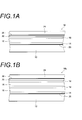
- FIG. 1A and FIG. 1B are diagrams conceptually illustrating an example of a functional film. It is a figure which shows notionally an example of the organic EL laminated body which sealed the organic EL device using the functional film shown by FIG. 1 (A).
- FIG. 1A conceptually shows an example of the functional film of the present invention.
- the functional film 10 has a protective inorganic film 14 on a support 12, an inorganic film 18, and an organic film 16 that is a base of the inorganic film 18, and an adhesive.
- the inorganic film 18 and the sealant layer 24 are bonded by the layer 20.
- the functional film 10 has a mixed layer 26 in which components of both layers are mixed between the adhesive layer 20 and the sealant layer 24.
- the functional film 10 has the mixed layer 28 (2nd mixed layer) by which both components were mixed between the support body 12 and the protective inorganic film
- the functional film 10 includes a mixed layer 28, a protective inorganic layer 14, an organic film 16, an inorganic film 18, an adhesive layer 20, and a mixed layer in this order from the support 12 side (the lower side in FIG. 1A). 26 and a sealant layer 24.
- the functional film 10 has one combination of the inorganic film 18 and the underlying organic film 16, but not limited to this, the functional film 10 includes the organic film 16 and the inorganic film 18. You may have two or more combinations. For example, the functional film 10 may have two combinations of the inorganic film 18 and the underlying organic film 16 as in the functional film 10b shown in FIG. Also good.
- the functional film 10 may have one or a combination of the underlying organic film 16 and the inorganic film 18, or may have a plurality of combinations, and the uppermost layer (support 12) of the laminated structure of the inorganic film 18 and the underlying organic film 16. The most separated film) is the inorganic film 18.
- the uppermost inorganic film 18 and the sealant layer 24 are bonded together by the adhesive layer 20.
- the functional film 10 is suitably used as a sealing substrate for the organic EL device 36.
- the organic EL device 36 includes a light emitting element 32 formed on an element substrate 30 such as a glass plate, and a passivation film 34 made of silicon nitride or the like and covering the light emitting element 32 (and the element substrate 30).
- the functional film 10 is formed by laminating the sealant layer 24 facing the passivation film 34 and melting the sealant layer 24 to heat the sealant layer 24 and the passivation film 34.
- the organic EL device 36 is sealed by fusing. Thereby, the organic EL laminated body in which the organic EL device 36 is sealed with the functional film 10 is formed.
- the functional film 10 is particularly preferably used as a sealing substrate for a top emission type organic EL device (organic EL device) that emits light on the side opposite to the element substrate 30 (passivation film 34 side). .
- the support 12 (substrate or base material) is a transparent sheet having a retardation value (Retardation) of 50 nm or less.
- the retardation value of the support 12 is preferably 20 nm or less, and more preferably 5 nm or less.
- the Tg of the support 12 is 160 to 180 ° C., for example.
- the support 12 a transparent one having a retardation value of 50 nm or less and being transparent can be used.
- the support 12 is preferably a plastic film made of polycarbonate (PC), cycloolefin polymer (COP), cycloolefin copolymer (COC), triacetylcellulose (TAC), transparent polyimide, or the like, having a retardation value of 50 nm or less. Illustrated.
- a plastic film having a retardation value of 50 nm or less is also referred to as a “low retardation film”.
- the support 12 has low moisture permeability and water content. A small amount is preferred.
- the support 12 is also excellent in flexibility. Considering this point, the support 12 is particularly preferably a low retardation film made of polycarbonate, cycloolefin polymer or cycloolefin copolymer.
- the support 12 is preferably a low retardation film made of a cycloolefin polymer or a cycloolefin copolymer.
- the support 12 is particularly preferably a low retardation film made of a cycloolefin copolymer.
- the thickness of the support 12 may be appropriately set according to the use and size of the functional film 10. According to the study of the present inventor, it was found that the thickness of the support 12 is preferably about 10 to 200 ⁇ m. By setting the thickness of the support 12 within this range, it is preferable in terms of weight reduction and thinning of an organic EL laminate (organic EL device) using the functional film 10 as a sealing substrate.
- the support body 12 may be formed by forming a film exhibiting a necessary function such as an antireflection film on the surface of the exemplified low retardation film.
- a protective inorganic film 14 is formed (deposited) on the surface of the support 12.
- the protective inorganic film 14 is a film made of an inorganic compound (a film (layer) containing an inorganic compound as a main component), and protects the support 12 when the organic film 16 is formed.
- the organic film 16 serving as the base of the inorganic film 18 is usually formed by a so-called coating method or flash vapor deposition. Specifically, the organic film 16 is formed using a paint in which an organic compound is dissolved in a solvent. In these methods, the coating material for forming the organic film 16 has a low boiling point such as methyl ethyl ketone (MEK) or methyl isobutyl ketone (MIBK) in order to ensure the coating property of the coating material and the smoothness of the surface of the formed film. It is preferable to include an organic solvent.
- MEK methyl ethyl ketone
- MIBK methyl isobutyl ketone
- a low retardation film generally tends to be dissolved or altered by an organic solvent. Therefore, when the organic film 16 is formed on the surface of the support 12 that is a low retardation film by a coating method or the like, the solvent may cause dissolution or alteration of the surface of the support 12 when the paint is applied. If dissolution or alteration of the surface of the support 12 occurs, the retardation value of the support 12 changes, light transmittance decreases, haze increases, and the optical characteristics of the functional film 10 deteriorate. To do. That is, even if a low retardation film is used for the support 12, the effect cannot be sufficiently exhibited. As a result, the performance of the organic EL device using the functional film 10 as a sealing substrate is degraded.
- the functional film 10 forms the protective inorganic film 14 on the surface of the support 12 which is a low retardation film, and forms a combination of the organic film 16 and the inorganic film 18 as a base thereon. Therefore, even if the functional film 10 forms the organic film
- the functional film 10 having high transparency and low haze and excellent optical properties can be realized.
- the material for forming the protective inorganic film 14 various inorganic compounds can be used as long as they can form a film that does not allow the organic solvent to permeate.
- the material for forming the protective inorganic film 14 include metal oxides such as aluminum oxide, magnesium oxide, tantalum oxide, zirconium oxide, titanium oxide, and indium tin oxide (ITO); metal nitrides such as aluminum nitride; metals such as aluminum carbide Carbides; Silicon oxides such as silicon oxide, silicon oxynitride, silicon oxycarbide, and silicon oxynitride carbide; silicon nitrides such as silicon nitride and silicon nitride carbide; and inorganic compounds such as silicon carbide such as silicon carbide Is done.
- metal oxides such as aluminum oxide, magnesium oxide, tantalum oxide, zirconium oxide, titanium oxide, and indium tin oxide (ITO)
- metal nitrides such as aluminum nitride
- metals such
- a hydride or hydrogen-containing material of the above-described inorganic compound and a mixture of two or more of the above-described inorganic compounds are also preferably used as the material for forming the protective inorganic film 14.
- silicon nitride, silicon oxide, silicon oxynitride, and aluminum oxide are preferably used because they are highly transparent and dense.
- silicon nitride is particularly preferably used because it is denser and highly transparent.
- the protective inorganic film 14 also exhibits gas barrier property like the inorganic film 18.
- the protective inorganic film 14 is preferably formed using the same material as the inorganic film 18 that mainly expresses the target gas barrier properties.
- the protective inorganic film 14 is preferably formed of silicon nitride that has high transparency and high gas barrier properties.
- the protective inorganic film 14 is formed of a silicon compound, it is preferable that at least one of —O group and —OH group is introduced on the surface of the protective inorganic film 14, and in particular, —OH group is introduced. It is preferable. Introduction of —OH groups or the like into the protective inorganic film 14 may be performed in the same manner as described later for the inorganic film 18. Adhesion between the protective inorganic film 14 and the organic film 16 is obtained by introducing —O groups or —OH groups on the surface of the protective inorganic film 14 on the surface layer and the organic film 16 containing a silane coupling agent. Can be more suitably secured. In this regard, the inorganic film 18 and the adhesive layer 20 are illustrated and described in detail later.
- the thickness of the protective inorganic film 14 is appropriately set according to the forming material so that the paint (organic solvent) forming the organic film 16 can be prevented from reaching the support 12. That's fine.
- the thickness of the protective inorganic film 14 is preferably 5 to 200 nm.
- the thickness of the protective inorganic film 14 is more preferably 10 to 100 nm.
- the protective inorganic film 14 exhibits gas barrier properties, which can improve the gas barrier properties, reduce the number of stacked organic films 16 and inorganic films 18, and the like. Moreover, it can prevent suitably that a crack and a crack generate
- the functional film 10 preferably has a mixed layer 28 (second mixed layer) in which both components are mixed between the support 12 and the protective inorganic film 14.
- the support 12 which is a low retardation film and the protective inorganic film 14 have completely different optical characteristics such as refractive index.
- the protective inorganic film 14 having completely different optical properties is directly laminated on the support 12, the optical properties may vary greatly between the layers due to the difference between the optical properties. For this reason, even if a low retardation film having a retardation value of 50 nm or less is used as the support 12, the optical characteristics may not be sufficiently exhibited.
- the mixed layer 28 in which the component of the support 12 and the component of the protective inorganic film 14 are mixed has intermediate optical characteristics. Therefore, the mixed layer 28 acts like a buffer layer that suppresses a rapid change in optical characteristics such as a refractive index between the support 12 and the protective inorganic film 14.
- the functional film 10 having excellent optical properties that further expresses the optical properties of the support 12 that is a low retardation film is obtained. be able to.
- damage to the functional film 10 (particularly the inorganic film 18) due to changes in temperature and humidity can be suitably prevented.
- the adhesion between the support 12 and the protective inorganic film 14 can be further improved.
- the protective inorganic film 14 made of an inorganic compound such as silicon nitride is usually formed by a vapor deposition method such as plasma CVD or sputtering, like the inorganic film 18.
- the mixed layer 28 obtained by mixing the components of the support 12 and the protective inorganic film 14 is subjected to etching of the support 12 by plasma or the support 12 when forming the protective inorganic film 14 by vapor deposition. It can be formed by controlling the drawing of ions or the like by the bias.
- the thickness of the mixed layer 28 is preferably 1 to 100 nm.
- the thickness of the mixed layer 28 is more preferably 2 to 30 nm, and further preferably 5 to 15 nm. If the thickness of the mixed layer 28 is less than 1 nm, the effect of forming the mixed layer 28 may not be sufficiently obtained. Conversely, if the thickness of the mixed layer 28 exceeds 100 nm, the mixed layer 28 is too thick, and there is a concern that the optical characteristics of the functional film 10 are deteriorated. On the other hand, if the thickness of the mixed layer 28 exceeds 100 nm, the mixed layer 28 may be cracked or cracked, and the gas barrier property may be lowered due to this.
- the thickness of the mixed layer 28 is measured as follows as an example.
- the cross section of the laminate in which the protective inorganic film 14 is formed on the surface of the support 12 is observed with a scanning electron microscope or the like, and the distance between the lower end (support 12 side) and the upper end of the mixed layer 28 (thickness direction)
- the thickness of the mixed layer 28 in this cross section is measured.
- the thickness of the cross section is measured at 10 arbitrarily selected positions (10 cross sections), and the average of the thicknesses of the mixed layer 28 at the 10 cross sections is defined as the total thickness of the mixed layer 28.
- the organic film 16 is formed on the protective inorganic film 14.
- the organic film 16 is a film made of an organic compound (a film (layer) containing an organic compound as a main component) and is basically obtained by crosslinking (polymerizing) at least one of a monomer and an oligomer.
- the Tg of the organic film 16 is 160 to 180 ° C., for example.
- the organic film 16 serves as a base layer for the inorganic film 18 that mainly exhibits gas barrier properties.
- the functional film 10 has an organic film 16 that serves as a base for the inorganic film 18, thereby embedding (covering) the irregularities on the surface of the support 12, foreign matters adhering to the surface, and the like.
- the formation surface (film formation surface) of the film 18 can be made appropriate.
- the organic film 16 By forming the organic film 16, the surface on which the inorganic film 18 is formed becomes more suitable for film formation. As a result, an appropriate inorganic film 18 can be formed on the entire formation surface without any gaps and without cracks or cracks.
- the functional film 10 of the present invention has such an organic and inorganic laminated structure, it has a high gas barrier performance in which the water vapor transmission rate is less than 1 ⁇ 10 ⁇ 4 [g / (m 2 ⁇ day)]. Obtainable. That is, by using the functional film 10 having an organic and inorganic laminated structure and high gas barrier performance as a sealing substrate for an organic EL device, it is possible to suitably prevent the light emitting element 32 from being deteriorate
- the organic film 16 serving as the base of the inorganic film 18 also functions as a cushion for the inorganic film 18. Therefore, the inorganic film 18 is damaged by the cushioning effect of the organic film 16 when the organic EL device 36 and the functional film 10 are pressed or when the organic EL device 36 receives an impact from the outside. Can be prevented. Thereby, in the organic EL device 36 as shown in FIG. 2, the functional film 10 appropriately exhibits the gas barrier performance, and the deterioration of the light emitting element 32 due to moisture can be suitably prevented.
- organic compounds can be used as the material for forming the organic film 16.
- polyester acrylic resin, methacrylic resin, methacrylic acid-maleic acid copolymer, polystyrene, transparent fluororesin, polyimide, fluorinated polyimide, polyamide, polyamideimide, polyetherimide, cellulose acylate , Polyurethane, polyether ether ketone, polycarbonate, alicyclic polyolefin, polyarylate, polyether sulfone, polysulfone, fluorene ring modified polycarbonate, alicyclic modified polycarbonate, fluorene ring modified polyester, acryloyl compound, thermoplastic resin, or poly Preferred examples include siloxane and other organosilicon compounds. A plurality of these may be used in combination.
- the material for forming the organic film 16 is preferably a polymer of a radical polymerizable compound and / or a cationic polymerizable compound having an ether group as a functional group in terms of excellent glass transition temperature and strength.
- an acrylate and / or methacrylate monomer or oligomer polymer is a main component in that the refractive index is low, the transparency is high, and the optical properties are excellent.
- An acrylic resin or a methacrylic resin having a glass transition temperature of 120 ° C. or higher is more preferable.
- the organic film 16 in particular, dipropylene glycol di (meth) acrylate (DPGDA), trimethylolpropane tri (meth) acrylate (TMPTA), dipentaerythritol hexa (meth) acrylate (DPHA), and the like.
- DPGDA dipropylene glycol di (meth) acrylate
- TMPTA trimethylolpropane tri (meth) acrylate
- DPHA dipentaerythritol hexa
- Acrylic resin and methacrylic resin which are mainly composed of a bifunctional or higher, especially trifunctional or higher, acrylate and / or methacrylate monomer or oligomer polymer, are more preferred.
- the material for forming the organic film 16 it is also preferable to use a plurality of these acrylic resins and methacrylic resins.
- the inorganic film 18 can be formed on a base having a solid (stable) skeleton, so that the inorganic film 18 with higher density and higher gas barrier properties is formed. Is done.
- the thickness of the organic film 16 is preferably 0.5 to 5 ⁇ m, and more preferably 1 to 3 ⁇ m.
- the thickness of the organic film 16 is preferably 0.5 to 5 ⁇ m, and more preferably 1 to 3 ⁇ m.
- the surface on which the inorganic film 18 is formed is more suitable. For this reason, an appropriate inorganic film 18 free from cracks and cracks is formed over a wider range of the formation surface.
- the thickness of the organic film 16 by setting the thickness of the organic film 16 to 0.5 ⁇ m or more, the effect as a cushion is sufficiently exhibited at the time of pressing when the organic EL device 36 and the functional film 10 are bonded, and the inorganic film 16 is inorganic. Damage to the film 18 can be prevented more reliably.
- the thickness of the organic film 16 is set to 5 ⁇ m or less, it is possible to suitably prevent the occurrence of problems such as cracks in the organic film 16 and curling of the functional film 10 due to the organic film 16 being too thick. can do.
- each organic film 16 When a plurality of organic films 16 are provided as in the gas barrier film shown in FIG. 1B, the thickness of each organic film 16 may be the same or different from each other. Moreover, when it has the some organic film 16, the formation material of each organic film 16 may be the same, and may differ. From the viewpoint of productivity and the like, it is preferable to form all the organic films 16 with the same material.
- the organic film 16 may be formed by a coating method, flash vapor deposition, or the like.
- the organic film 16 preferably contains a silane coupling agent.
- the protective inorganic film 14 is formed of a silicon compound, -OH groups or the like are introduced on the surface of the protective inorganic film 14, and the organic film 16 contains a silane coupling agent, whereby the inorganic film 18 and the adhesive layer 20 The adhesion between the protective inorganic film 14 and the organic film 16 can be ensured by the same action as described later.
- an inorganic film 18 is formed using the organic film 16 as a base.
- the inorganic film 18 is a film made of an inorganic compound (film (layer) containing an inorganic compound as a main component), and the functional film 10 mainly exhibits gas barrier properties.
- the uppermost layer is the inorganic film 18, and the uppermost inorganic film 18 and the sealant layer 24 are bonded by the adhesive layer 20.
- the inorganic film 18 various kinds of films made of an inorganic compound that exhibits gas barrier properties can be used.
- a film made of the inorganic compound exemplified in the above protective inorganic film 14 is preferably exemplified.
- a film made of a silicon compound is suitable because it is highly transparent and can exhibit excellent gas barrier properties.
- a film made of silicon nitride is particularly preferable because it has high transparency in addition to excellent gas barrier properties.
- each inorganic film 18 may mutually differ. Considering productivity and the like, it is preferable to form all the inorganic films 18 with the same material.
- the inorganic film 18 and the protective inorganic film 14 may be formed of different materials. Considering productivity and the like, the inorganic film 18 and the protective inorganic film 14 are preferably formed of the same material.
- the inorganic film 18 is formed of a silicon compound, it is preferable that at least one of —O groups and —OH groups is introduced on the surface of the uppermost inorganic film 18, and in particular, —OH groups are introduced. It is preferable. In particular, it is preferable that the uppermost inorganic film 18 is formed of silicon nitride, and at least one of —O groups and —OH groups, in particular —OH groups, is introduced into the surface thereof. Adhesiveness between the inorganic film 18 and the adhesive layer 20 is obtained by introducing —O groups or —OH groups on the surface of the surface inorganic film 18 and the adhesive layer 20 containing a silane coupling agent. Can be more suitably secured. This will be described in detail later.
- the thickness of the inorganic film 18 may be determined as appropriate according to the forming material so that the target gas barrier property can be exhibited. According to the study by the inventors, it has been found that the thickness of the inorganic film 18 is preferably 10 to 200 nm. The thickness of the inorganic film 18 is preferably 10 to 100 nm, and more preferably 20 to 75 nm. By setting the thickness of the inorganic film 18 to 10 nm or more, the inorganic film 18 that stably expresses sufficient gas barrier performance can be formed. Further, the inorganic film 18 is generally fragile, and if it is too thick, there is a possibility of causing cracks, cracks, peeling, and the like.
- membrane 18 being 200 nm or less.
- the thickness of each inorganic film 18 may be the same or different.
- the functional film 10 preferably has a water vapor transmission rate of 1 ⁇ 10 ⁇ 4 [g / (m 2 ⁇ day)] before the adhesive layer 20 and the sealant layer 24 are formed.
- the inorganic film 18 can be formed by a known method.
- a vapor deposition method such as plasma CVD such as CCP-CVD or ICP-CVD, sputtering such as magnetron sputtering or reactive sputtering, or vacuum deposition is preferably exemplified. Is done.
- a film made of a silicon compound formed by a vapor deposition method not all of the silicon in the film forms a target compound such as silicon nitride, and has unbonded bonds. Silicon is also present. In particular, a large amount of silicon having unbonded bonds is present on the surface of the film. Therefore, after the inorganic film 18 is formed, the surface of the film is exposed to air (atmosphere), whereby —O groups and —OH groups are bonded to the unbonded bonds. In this way, —O groups and —OH groups (particularly —OH groups) are introduced onto the surface of the inorganic film 18 as described above.
- a sealant layer (thermal welding layer) 24 is bonded by an adhesive layer 20.
- the sealant layer 24 thermally welds (heat seals or heat seals) the functional film 10 to the organic EL device 36 (passivation film 34) or the like.
- the sealant layer 24 is formed of a material having a retardation value of 300 nm or less and a glass transition temperature (Tg) lower than that of the support 12.
- the functional film 10 has a protective inorganic film 14 on a support 12 that is a low retardation film, and an organic and inorganic film including an inorganic film 18 and a base organic film 16 thereon. It has a laminate structure. That is, the functional film 10 has a low retardation, a low retardation, and a low retardation sealant layer 24 formed by an adhesive layer 20 on a gas barrier film having an organic and inorganic laminated structure. It is glued.
- the organic EL device is also required to be flexible enough to be bent.
- a plastic film as the sealing substrate for sealing the organic EL device 36.
- FIG. 2 by sealing the organic EL device 36 using the functional film 10 as a sealing substrate, a conventional organic EL laminate using a glass plate or the like as the sealing substrate is obtained.
- the weight can be reduced and the thickness can be reduced.
- the functional film 10 is used as a sealing substrate, the weight and thickness are reduced in the same manner as when a plastic film is used as a sealing substrate.
- the functional film 10 Since the functional film 10 is bonded to the organic EL device 36 by heat welding with the sealant layer 24, the melted sealant layer 24 follows the unevenness of the organic EL device 36 (passivation film 34). For this reason, the functional film 10 fills the unevenness
- the functional film 10 has a support 12 and a sealant layer 24 with low retardation, and has a protective inorganic film 14.
- the organic EL device 36 when the organic EL device 36 is sealed, the adverse effect of the functional film 10 on the optical characteristics of the organic EL device 36 is suppressed. As a result, an organic EL device having excellent optical characteristics such as a high-quality organic EL display can be manufactured.
- the functional film 10 is thermally welded to the organic EL device 36 or the like. At this time, the sealant layer 24 of the functional film 10 is melted and solidified again. At this time, it is considered that the sealant layer 24 becomes Tg or more and adhesion is performed without stretching. As a result, the retardation value is lowered, and an organic EL laminate having more excellent optical characteristics is formed.
- the functional film 10 has an organic and inorganic laminated structure, and has a high gas barrier performance with a water vapor permeability of less than 1 ⁇ 10 ⁇ 4 [g / (m 2 ⁇ day)]. Therefore, it can prevent more suitably that the light emitting element 32 of the organic EL device 36 deteriorates with moisture by using the functional film 10 as a sealing substrate.
- the Tg of the sealant layer 24 is lower than the Tg of the support 12, the support 12 can maintain its own strength during heat welding. Therefore, the inorganic film 18 and the like are prevented from being damaged by deformation of the support 12 and the functional film 10 can appropriately exhibit excellent gas barrier performance.
- the functional film 10 can be thermally welded to the organic EL device 36 at a lower temperature by making the Tg of the sealant layer 24 lower than the Tg of the support 12.
- the sealant layer 24 is a sheet-like material having a retardation value of 300 nm or less and a Tg lower than that of the support 12.
- the Tg of the sealant layer 24 is 40 to 90 ° C., for example.
- the functional film 10 is suitably used for sealing a top emission type organic EL device. Therefore, when the retardation value of the sealant layer 24 exceeds 300 nm, the same problems as the above-described decrease in light utilization efficiency and image quality deterioration of the organic EL display occur with respect to the support 12.
- the retardation value of the sealant layer 24 is preferably 200 nm or less, more preferably 150 nm or less, still more preferably 100 nm or less, and particularly preferably 50 nm or less.
- the sealant layer 24 having the above retardation value and having a Tg lower than that of the support 12 can be used.
- a plastic film formed of a material having a low Tg and having a retardation value of 300 nm or less among the materials forming the low retardation film exemplified for the support 12 is preferably exemplified.
- these materials and various components for example, polyethylene (PE) or the like
- PE polyethylene
- a plastic film formed of a material having a low Tg and having a retardation value of 300 nm or less is also suitable. Illustrated.
- a plastic film having a retardation value of 300 nm or less may be referred to as a “low retardation film”.
- the sealant layer 24 is made of, in particular, a low Tg polycarbonate (low Tg), a low retardation film made of a cycloolefin polymer or a cycloolefin copolymer, or a low Tg blended with these materials.
- a low retardation film made of a material is suitable.
- a low retardation film composed of a low Tg cycloolefin polymer or a cycloolefin copolymer, or a low retardation film composed of a low Tg material containing these materials is suitable as the sealant layer 24.
- a low retardation film made of a low Tg cycloolefin copolymer or a low retardation film made of a low Tg material blended with a low Tg cycloolefin copolymer is particularly preferably exemplified as the sealant layer 24.
- the support 12 and the sealant layer 24 are preferably formed of similar materials.
- the material for forming the support 12 is cycloolefin-based (for example, cycloolefin copolymer (COC) or cycloolefin polymer (COP))
- the material for forming the sealant layer 24 is also cycloolefin-based (COC or COP).
- the material for forming the support 12 and the sealant layer 24 is both polycarbonate (PC) or cellulose (for example, triacetyl cellulose (TAC)).
- the Tg of the sealant layer 24 may be lower than the Tg of the support 12, but it is preferable that the difference between the two Tg is larger.
- the Tg of the sealant layer 24 is preferably 50 ° C. or more lower than the Tg of the support 12, and particularly preferably 80 ° C. or more.
- the sealant layer 24 is a gas barrier having a water vapor transmission rate measured in accordance with, for example, JIS Z 0208 of less than 50 [g / (m 2 ⁇ day)] when converted to 100 ⁇ m in an environment of 60 ° C. and 90% RH. It is preferable to have properties.
- JIS Z 0208 As the cause of deterioration of the light emitting element 32 when the organic EL device 36 is sealed, moisture entering from the end of the sealant layer 24 and outgas from the adhesive layer 20 and the mixed layer 26 are assumed. In particular, the outgas from the adhesive layer 20 and the mixed layer 26 exists in the space between the inorganic film 18 having gas barrier properties and the passivation film 34.
- this outgas does not have a refuge at the time of heat welding or the like, and may have a great adverse effect on the light emitting element 32.
- the water vapor transmission rate of the sealant layer 24 is less than 50 [g / (m 2 ⁇ day)]
- Deterioration of the light emitting element 32 due to outgassing is preferably prevented.
- the sealant layer 24 is too thick, moisture that causes deterioration of the light emitting element 32 easily enters from the end of the sealant layer 24.
- the sealant layer 24 sufficiently fills the unevenness of the surface of the organic EL device 36 and the inorganic film 18 is damaged by the unevenness. It must also have an effect as a cushion to prevent. For this reason, it is preferable that the sealant layer 24 has a certain thickness. Considering the above points, the thickness of the sealant layer 24 is preferably 5 to 100 ⁇ m, more preferably 10 to 70 ⁇ m.
- the adhesive layer 20 various adhesives can be used as long as they can adhere the inorganic film 18 and the sealant layer 24 and do not adversely affect the optical characteristics of the functional film 10.
- the Tg of the adhesive layer 20 is, for example, 120 to 150 ° C.
- the adhesive layer 20 is exemplified by an adhesive such as an epoxy resin, an acrylic resin, and a urethane resin.
- an acrylic resin adhesive is preferably used in terms of optical characteristics and the like.
- the adhesive layer 20 preferably contains a silane coupling agent.
- the inorganic film 18 bonded to the sealant layer 24 by the adhesive layer 20 preferably has —O groups and / or —OH groups introduced on the surface. Thereby, the adhesive force of the adhesive bond layer 20 and the inorganic film
- the silane coupling agent is obtained by bonding a hydrolyzable group such as an alkoxy group and an organic functional group that can be expected to react and interact with an organic substance such as an amino group to silicon.
- the silane coupling agent is converted into —OH group by hydrolyzing the hydrolyzable group, and dehydration condensation between this —OH group and —OH group on the surface of the inorganic compound results in strong strength between the surface of the inorganic compound. causess a covalent bond.
- the silane coupling agent is firmly bound to the organic compound by copolymerization of an organic functional group and the organic compound. Thereby, a silane coupling agent improves the adhesiveness of organic substance and inorganic substance.
- the inorganic film 18 is a silicon compound
- —O group preferably —OH group
- —OH group a state like “SiOH”
- Hydrolysis reaction of the silane coupling agent occurs due to the released —OH group or the like, and the silicon compound and the silane coupling agent are bonded by a covalent bond by dehydration condensation. In this way, higher adhesion between the adhesive layer 20 and the inorganic film 18 is obtained.
- a pH adjuster is added (acid or alkali is added) to adjust the pH.
- a pH adjuster is added to an adhesive containing a silane coupling agent, hydrolysis proceeds due to atmospheric humidity or water supply from an organic solvent, causing problems such as an increase in viscosity of the adhesive.
- the adhesive layer 20 contains a silane coupling agent and an -O group or OH group is introduced on the surface of the inorganic film 18 made of a silicon compound, a pH adjuster is added to adjust the pH. Even without adjustment, high adhesion can be obtained. That is, according to this configuration, it is possible to omit from the adhesive layer 20 a pH adjuster that may cause inconvenience.
- the adhesive layer 20 is thin as long as the inorganic film 18 and the sealant layer 24 can be bonded together.
- the adhesive layer 20 is preferably thinner than the sealant layer 24. Therefore, the thickness of the adhesive layer 20 is preferably 10 ⁇ m or less, and particularly preferably 5 ⁇ m or less.
- the Tg of the sealant layer 24 is lower than the Tg of the support 12.
- the Tg of the sealant layer 24 is lower than the Tg of the adhesive layer 20
- the Tg of the adhesive layer 20 is preferably lower than the Tg of the support 12 and the Tg of the organic film 16.
- the Tg of the sealant layer 24 is preferably 60 ° C. or more lower than the Tg of the adhesive layer 20, and more preferably 80 ° C. or less.
- the Tg of the adhesive layer 20 is preferably 30 ° C. or more lower than the Tg of the support 12 (and the organic film 16), and more preferably 40 ° C. or less.
- the adhesive layer 20 can suppress the deformation from being transmitted to the inorganic film 18. Furthermore, even if the sealant layer 24 (adhesive layer 20) is deformed when the functional film 10 is heat-sealed, the inorganic film 18 (protective inorganic film 14) can be supported by the organic film 16 and the support 12. . Therefore, by having this configuration, it is possible to suitably prevent the inorganic film 18 from being damaged following the deformation of the sealant layer 24 when the functional film 10 is heat-sealed.
- the adhesive layer 20 is preferably highly flexible. Specifically, the adhesive layer 20 preferably has a pencil hardness of 3H or lower and lower than the pencil hardness of the organic film 16. By having such a configuration, the adhesive layer 20 is prevented from obstructing the flow of the sealant layer 24 when the functional film 10 is heat-sealed, so that more reliable heat-welding is possible. Moreover, even if the adhesive layer 20 is deformed at the time of heat welding, the organic film 16 can support the inorganic film 18, so that the inorganic film 18 can be more reliably prevented from being damaged.
- the functional film 10 has the mixed layer 26 by which the component of the adhesive bond layer 20 and the component of the sealant layer 24 were mixed between the adhesive bond layer 20 and the sealant layer 24 as a preferable aspect.
- the sealant layer 24 is a low retardation film having a retardation value of 300 nm or less. Further, the sealant layer 24 and the adhesive layer 20 often have completely different optical characteristics such as a refractive index. When the adhesive layer 20 having completely different optical characteristics is directly laminated on the sealant layer 24, the optical characteristics may vary greatly between the layers due to the difference in optical characteristics. Therefore, even when a low retardation film having a retardation value of 300 nm or less is used as the sealant layer 24, the optical characteristics may not be sufficiently exhibited.
- the mixed layer 26 in which the component of the adhesive layer 20 and the component of the sealant layer 24 are mixed has intermediate optical characteristics. Therefore, the mixed layer 26 acts like a buffer layer that suppresses a rapid change in optical characteristics such as a refractive index between the adhesive layer 20 and the sealant layer 24. Therefore, by having such a mixed layer 26 between the adhesive layer 20 and the sealant layer 24, the optical properties of the sealant layer 24, which is a low retardation film, are further expressed and have excellent optical properties.
- the functional film 10 can be obtained.
- the adhesive force between the adhesive layer 20 and the sealant layer 24 is increased, and the peeling between the two layers is more preferably performed. Can be prevented.
- the adhesive layer 20 can suitably follow the deformation of the sealant layer 24 when performing heat welding, and can maintain the adhesion, and the inorganic film 18 can be used as the sealant layer 24. It is also possible to prevent damage following the deformation.
- the mixed layer 26 is applied with an adhesive (coating material) to be the adhesive layer 20, and after the sealant layer 24 (low retardation film to be the sealant layer 24) is laminated, before the adhesive is cured, It is formed by heating the sealant layer 24 to a temperature higher than the Tg of the sealant layer 24 and curing the adhesive while melting the sealant layer 24.
- the melt of the sealant layer 24 for forming the mixed layer 26 is sufficient in a short time, for example, about 1 to 60 seconds.
- the mixed layer 26 sufficiently exhibits the above-described effect even if it is extremely thin, but it is preferable to have a thickness that does not affect the optical characteristics of the functional film 10.
- the thickness of the mixed layer 26 is preferably about 5 to 100 nm, and particularly preferably about 10 to 50 nm.
- the thickness of the mixed layer 26 may be measured in the same manner as the measurement method described for the mixed layer 28.
- the functional film 10 has a retardation value of preferably 300 nm or less, more preferably 100 nm or less, and particularly preferably 50 nm or less as a whole laminate in which the sealant layer 24 is laminated.
- the functional film 10 can be manufactured using the following film formation method or the like.
- the protective inorganic film 14 is formed on the surface of the low retardation film to be the support 12 by plasma CVD.
- an organic film 16 is formed on the protective inorganic film 14 by a coating method, and an inorganic film 18 is further formed on the organic film 16 by plasma CVD.
- a mixed layer 28 (second mixed layer) in which the component of the support 12 and the component of the protective inorganic film 14 are mixed.
- an adhesive is applied to the surface of the inorganic film 18 and a low retardation film to be the sealant layer 24 is laminated.
- the adhesive is cured by irradiating with ultraviolet rays, heating or the like while pressing the laminate as necessary.
- the inorganic film 18 and the sealant layer 24 are bonded by the adhesive layer 20 to obtain the functional film 10.
- the sealant layer 24 is heated to a temperature equal to or higher than the Tg of the sealant layer 24, and the sealant layer 24 is melted and bonded. .
- the mixed layer 26 can be formed between the adhesive layer 20 and the sealant layer 24.
- the lamination of the sealant layer 24 by RtoR may include one or more of application of an adhesive to be the adhesive layer 20, curing of the adhesive, and formation of the mixed layer 26.
- RtoR refers to the process of continuously sending out the substrate to be processed from a substrate roll obtained by winding a long substrate to be processed into a roll, and transporting it in the longitudinal direction while forming each film, bonding the sealant layer 24, and the like.
- the functional film 10 can be manufactured with good production efficiency.
- you may perform all the processes by sending out and winding up the to-be-processed substrate once.
- each film may be formed and the sealant layer 24 may be bonded together by feeding and winding the separate substrates to be processed.
- one or more appropriately selected processes such as the formation of the organic film 16 and the formation of the inorganic film 18 are performed by feeding and winding the substrate to be processed once, and the substrate to be processed is wound and wound once. You may make it carry out.
- the functional film 10 may be manufactured by a so-called single wafer type (batch type) manufacturing method in which not only RtoR but also each film is formed on the cut sheet-like support 12.
- the functional film 10 is laminated on the organic EL device 36 with the passivation film 34 and the sealant layer 24 facing each other.
- the functional film 10 is heated from the support 12 side to bring the sealant layer 24 to a temperature equal to or higher than Tg and melt the sealant layer 24.
- the functional film 10 is pressed against the organic EL device 36, and the functional film 10 and the organic EL device 36 are thermally welded to obtain an organic EL laminate.
- the functional film 10 has a protective inorganic film 14 on the surface of the support 12, the retardation value of the support 12 is 50 nm or less, the retardation value of the sealant layer 24 is 300 nm or less, and the support 12 Tg is higher than Tg of the sealant layer 24. For this reason, it is suppressed that the inorganic film 18 is damaged by the flow of the sealant layer 24 during the thermal welding. Moreover, the organic EL laminated body after sealing also prevents the optical properties of the organic EL device 36 from being impaired.
- Example 1 As the support 12, a COP film (Arton film manufactured by JSR) having a thickness of 100 ⁇ m, a width of 1000 mm, and a length of 50 m was prepared. This support 12 has a retardation value of 3 nm and a Tg of 135 ° C.
- the support 12 was loaded into a general plasma CVD apparatus, and a protective inorganic film 14 having a thickness of 25 nm made of silicon nitride was formed by plasma CVD (CCP-CVD).
- Silane gas (SiH 4 ), ammonia gas (NH 3 ), nitrogen gas (N 2 ), and hydrogen gas (H 2 ) were used as source gases.
- the supply amount of each gas was 100 sccm for silane gas, 200 sccm for ammonia gas, 500 sccm for nitrogen gas, and 500 sccm for hydrogen gas.
- the forming pressure (film forming pressure) was 50 Pa.
- the plasma excitation power to be supplied was 3000 W at a frequency of 13.56 MHz. During film formation, bias power of 500 W was supplied to the support 12 side (substrate holder) at a frequency of 400 kHz.
- the paint for forming the organic film 16 is MEK (methyl ethyl ketone), TMPTA (trimethylolpropane triacrylate: manufactured by Daicel-Cytec), surfactant (BYK378 manufactured by BYK Chemie Japan), photopolymerization initiator (Ciba Chemicals). Irg 184) and a silane coupling agent (KBM5103 manufactured by Shin-Etsu Silicone Co., Ltd.) were added to prepare.
- the addition amount of the surfactant is 1% by mass at a concentration excluding MEK
- the addition amount of the photopolymerization initiator is 2% by mass at the concentration excluding MEK
- the addition amount of the silane coupling agent is 10 at the concentration excluding MEK. It was set as mass%.
- the solid content concentration of the paint obtained by diluting these components in MEK was 15% by mass. This paint was applied to the surface of the support 12 on which the protective inorganic film 14 was formed using a die coater. Subsequently, the coating material was dried with 80 degreeC drying air. Polymerization was performed by irradiating the dried paint with ultraviolet rays to form an organic film 16.
- the support 12 on which the organic film 16 was formed was loaded again into the plasma CVD apparatus described above, and an inorganic film 18 having a thickness of 50 nm made of silicon nitride was formed by plasma CVD (CCP-CVD).
- the inorganic film 18 was formed under the same conditions using the same source gas as that of the protective inorganic film 14 described above.
- the laminate in which the protective inorganic film 14, the organic film 16, and the inorganic film 18 were formed on the support 12 was cut into a sheet of 100 ⁇ 100 mm.
- Two kinds of epoxy resins JER1001 and JER152 manufactured by Japan Epoxy Resin
- photopolymerization initiator Irg184 manufactured by Ciba Chemicals
- silane coupling agent KBM502 manufactured by Shin-Etsu Silicone
- An agent a coating material to become the adhesive layer 20
- the addition amount of the two epoxy resins is 47% by mass excluding MEK
- the addition amount of the photopolymerization initiator is 2% by mass excluding MEK
- the addition amount of the silane coupling agent is excluding MEK.
- the concentration was 4% by mass.
- the solid content concentration of the paint obtained by diluting these components in MEK was 50% by mass.
- sealant layer 24 COC and PE (LLDPE) were blended to produce a 100 ⁇ 100 mm film having a thickness of 50 ⁇ m.
- This sealant layer 24 has a retardation value of 100 nm and a Tg of 50 ° C.
- the prepared adhesive was applied to the surface of the cut-sheet laminated inorganic film 18 using a bar coater.
- the adhesive was applied so that the thickness of the adhesive layer 20 was 10 ⁇ m.
- the adhesive was dried in an oven at 100 ° C. for 1 minute.
- a sealant layer 24 was laminated on the dried adhesive.
- the adhesive was cured by irradiating ultraviolet rays, and the inorganic film 18 and the sealant layer 24 were adhered by the adhesive layer 20.
- the functional film 10 was produced.
- the substrate 12 was heated from the side of the support 12 with a hot plate, and the temperature of the support 12 was kept at 80 ° C. for 30 seconds.
- a mixed layer 28 having a thickness of 25 nm was formed between the support 12 and the protective inorganic film 14, and the adhesive layer 20 and A mixed layer 26 having a thickness of 30 nm was formed between the sealant layer 24 and the sealant layer 24.
- the method for measuring the thickness of the mixed layer is as described above.
- Example 2 When forming the protective inorganic film
- Example 3 A functional film 10 was produced in the same manner as in Example 1 except that the bias power supplied to the support 12 side when forming the protective inorganic film 14 was 300 W. When confirmed in the same manner as in Example 1, a mixed layer 28 having a thickness of 10 nm was formed between the support 12 and the protective inorganic film 14.
- Example 4 A functional film 10 was produced in the same manner as in Example 1 except that heating was not performed simultaneously with the curing of the paint (adhesive) to be the adhesive layer 20. When the cross section of the functional film 10 was confirmed as in Example 1, the mixed layer 26 was not formed between the adhesive layer 20 and the sealant layer 24.
- Example 5 A functional film 10 was produced in the same manner as in Example 1 except that the temperature of the support 12 was maintained at 60 ° C. in the heating performed simultaneously with the curing of the paint (adhesive) to be the adhesive layer 20. As in Example 1, when the cross section of the functional film 10 was confirmed, a mixed layer 26 having a thickness of 20 nm was formed between the adhesive layer 20 and the sealant layer 24.
- Example 1 A functional film was produced in the same manner as in Example 1 except that the sealant layer 24 was changed to a COP film having a thickness of 100 ⁇ m (Arton film manufactured by JSR). This sealant layer 24 has a retardation value of 5 nm and a Tg of 142 ° C.
- Example 2 A functional film is produced in the same manner as in Example 1, except that COC and PE (LLDPE) are blended in a larger amount than in Example 1 to produce a film that becomes the sealant layer 24. did.
- the sealant layer 24 has a retardation value of 500 nm and a Tg of 40 ° C.
- Example 3 A functional film was produced in the same manner as in Example 1 except that the support 12 was changed to a polyethylene terephthalate film (Cosmo Shine manufactured by Toyobo Co., Ltd.) having a thickness of 100 ⁇ m, a width of 1000 mm, and a length of 50 m. .
- This support 12 has a retardation value of 306 nm and a Tg of 90 ° C.
- the support 12 is changed to a COC film (Appel, manufactured by Mitsui Chemicals) having a thickness of 100 ⁇ m, a width of 1000 mm, and a length of 50 m, and the sealant layer 24 is changed to a COC film (Eiwa) having a thickness of 50 ⁇ m.
- a functional film was produced in the same manner as in Example 1 except that the product was changed to “Opcon”.
- This support 12 has a retardation value of 5 nm and a Tg of 125 ° C.
- the sealant layer 24 has a retardation value of 5 nm and a Tg of 130 ° C.
- a glass plate having a thickness of 500 ⁇ m and 20 ⁇ 20 mm was prepared as the element substrate 30.
- the periphery of this element substrate 30 was masked with ceramic.
- the element substrate 30 subjected to masking was loaded into a general vacuum deposition apparatus, and an electrode made of metallic aluminum having a thickness of 100 nm was formed by vacuum deposition. Subsequently, a lithium fluoride layer having a thickness of 1 nm was formed.
- the element substrate 30 on which these organic compound layers are formed is loaded into a general sputtering apparatus, and a thickness of 0.2 ⁇ m is formed by DC magnetron sputtering using ITO (Indium Tin Oxide) as a target. A transparent electrode made of an ITO thin film was formed. Thus, the light emitting element 32 using the organic EL material was formed.
- ITO Indium Tin Oxide
- the masking was removed from the element substrate 30 on which the light emitting element 32 was formed.
- the element substrate 30 from which the masking was removed was loaded into a general plasma CVD apparatus, and a 1500 nm thick passivation film 34 made of silicon nitride was formed by plasma CVD (CCP-CVD).
- CCP-CVD plasma CVD
- the organic EL device 36 was produced. That is, the organic EL device 36 has a configuration in which one light emitting element 32 is formed in the center, and a passivation film 34 is formed so as to cover the entire surface of the light emitting element 32 and the element substrate 30.
- Silane gas (SiH 4 ), ammonia gas (NH 3 ), nitrogen gas (N 2 ), and hydrogen gas (H 2 ) were used as source gases for forming the passivation film 34.
- the supply amount of each gas was 100 sccm for silane gas, 200 sccm for ammonia gas, 500 sccm for nitrogen gas, and 500 sccm for hydrogen gas.
- the forming pressure was 50 Pa.
- the plasma excitation power to be supplied was 3000 W at a frequency of 13.56 MHz.
- the functional film was pressed against the organic EL device 36, and the functional film and the organic EL device 36 were thermally welded.
- the organic electroluminescent laminated body which sealed the organic electroluminescent device 36 with the functional film as shown in FIG. 2 was produced.
- the produced organic EL laminate was left in an environment of a temperature of 60 ° C. and a humidity of 90% RH for 200 hours.
- each organic EL laminated body was made to emit light by applying a voltage of 7 V using an SMU2400 type source measure unit manufactured by Keithley. Observation with a microscope from the support 12 side of the functional film confirmed the presence or absence of dark spots. About each organic EL laminated body, gas barrier property was evaluated based on the following references
- AA when the area of the dark spot portion is 0.1% or less of the area of the light emitting element 32; A when the area of the dark spot portion is more than 0.1% and not more than 1% of the area of the light emitting element 32; B when the area of the dark spot portion is more than 1% and not more than 3% of the area of the light emitting element 32; C when the area of the dark spot portion is more than 3% of the area of the light emitting element 32;
- Total light transmittance> The total light transmittance of the produced functional film was measured based on JIS K 7361 using NDH5000 manufactured by Nippon Denshoku Industries Co., Ltd.
- the functional films 10 of Examples 1 to 5 exhibit better gas barrier properties when the organic EL element is sealed as compared with Comparative Examples 1 to 4, and also, the optical properties such as total light transmittance, haze, retardation value (Re) and the like are excellent.
- the functional films 10 of Examples 1 to 5 have good gas barrier properties while suppressing deterioration of optical properties.
- the mixed layer 28 was not confirmed between the support 12 and the protective inorganic film 14, and in Example 3, the mixed layer 28 was as thin as 10 nm. It is considered that the optical characteristics have been lowered.
- the mixed layer 26 was not confirmed between the adhesive layer 20 and the sealant layer 24.
- Example 5 the mixed layer 26 was as thin as 20 nm, and thus the adhesion between the two layers was slightly weak. It is thought that some moisture entered. For this reason, Examples 4 and 5 are considered to have lower gas barrier properties and lower optical properties than Example 1.
- the Tg of the sealant layer 24 is higher than the Tg of the support 12. For this reason, when the organic EL device 36 is sealed, it is considered that the inorganic film 18 and the like are destroyed by the deformation of the support 12 and the gas barrier property is lowered.
- the retardation value of the sealant layer 24 is high, and in Comparative Example 3, the retardation value of the support 12 is high. For this reason, it is thought that the optical characteristic of the functional film has become low.
- the Tg of the sealant layer 24 is higher than the Tg of the support 12. For this reason, when the organic EL device 36 is sealed, it is considered that the inorganic film 18 and the like are destroyed by the deformation of the support 12 and the gas barrier property is lowered. From the above results, the effects of the present invention are clear.
Landscapes
- Physics & Mathematics (AREA)
- Optics & Photonics (AREA)
- Thermal Sciences (AREA)
- Chemical & Material Sciences (AREA)
- Inorganic Chemistry (AREA)
- Electroluminescent Light Sources (AREA)
- Laminated Bodies (AREA)
Abstract
Description
しかしながら、この方法では、金属やガラスによって装置全体を封止するので、有機ELデバイスが、重く、厚いものになってしまう。また、近年、有機ELディスプレイ等の有機ELデバイスを利用する有機EL装置に要求されているフレキシブル化への対応も、この方法では困難である。
具体的には、素子基板の上に有機EL材料や電極等を有する発光素子を、ガスバリア性を有するパッシベーション膜(保護膜)で覆い、このパッシベーション膜の上に封止基板を接着剤を用いて接着した積層体構造(有機EL積層体)とすることで、水分による発光素子の劣化を防止している。
また、封止基板の形成材料としては、ガラス、プラスチック、石英、樹脂、金属等が例示されている。
また、より良好に装置の軽量化や薄手化を図るためには、封止基板としてガラス等を用いるのと比較して、プラスチックフィルムを用いる方が有利である。
一方、特許文献3や特許文献4等に示されるような、加熱されることで溶融して、部材同士等を接着する、いわゆる熱溶着を行うシーラント材も知られている。周知のように、有機ELデバイスの表面は、形成された発光素子に応じた凹凸を有する。このようなシーラント材を用いて、封止基板を熱溶着することにより、溶融したシーラント剤で有機ELデバイスの表面の凹凸を埋めつつ、有機ELデバイスを封止基板によって封止できる。
しかしながら、本発明者の検討によれば、シーラント材を用いてプラスチックフィルムによって有機ELデバイスを封止すると、シーラント材とプラスチックフィルムとの層間の剥離や、特にトップエミッション型の有機ELデバイスでは光学特性の劣化など、様々な問題が生じる。
また、支持体と保護無機膜との間に、支持体の成分と保護無機膜の成分とが混合された第2混合層を有するのが好ましい。
また、シーラント層のガラス転移温度が接着剤層よりも低く、接着剤層のガラス転移温度が支持体および有機膜よりも低いのが好ましい。
また、シーラント層の厚さが10~100μmであり、かつ、接着剤層がシーラント層よりも薄いのが好ましい。
また、支持体とシーラント層とが、同系の材料で形成されるのが好ましい。
また、支持体およびシーラント層の少なくとも一方が、シクロオレフィンコポリマーで形成されるのが好ましい。
また、接着剤層がシランカップリング剤を有し、組み合わせのうち最も上に形成される無機膜がケイ素化合物の膜であり、この膜の表面に-O基および-OH基の少なくとも一方が導入されているのが好ましい。
さらに、保護無機膜および無機膜が窒化ケイ素の膜であるのが好ましい。
機能性フィルム10は、支持体12の上に、保護無機膜14を有し、この上に、無機膜18と、この無機膜18の下地となる有機膜16とを有し、さらに、接着剤層20によって、無機膜18と、シーラント層24とを接着してなるものである。機能性フィルム10は、好ましい態様として、接着剤層20とシーラント層24との間に、両層の成分が混合された混合層26を有する。また、機能性フィルム10は、好ましい態様として、支持体12と保護無機膜14との間に、両者の成分が混合された混合層28(第2混合層)を有する。本実施形態において機能性フィルム10は、支持体12側(図1(A)において下側)から順に、混合層28、保護無機層14、有機膜16、無機膜18、接着層20、混合層26及びシーラント層24を有する。
例えば、機能性フィルム10は、図1(B)に示す機能性フィルム10bのように、無機膜18と下地の有機膜16との組み合わせを2つ有してもよいし、3以上有してもよい。機能性フィルム10は、下地の有機膜16と無機膜18との組み合わせを1つ有する場合でも、複数有する場合でも、無機膜18と下地の有機膜16との積層構造の最上層(支持体12と最も離間する膜)は、無機膜18である。最上層の無機膜18とシーラント層24とが、接着剤層20によって接着される。
具体的には、図2に示すように、機能性フィルム10は、シーラント層24をパッシベーション膜34に対面して積層し、シーラント層24を溶融してこのシーラント層24とパッシベーション膜34とを熱融着することで、有機ELデバイス36を封止する。これにより、有機ELデバイス36が機能性フィルム10で封止された有機EL積層体が形成される。
中でも、機能性フィルム10は、素子基板30と逆側(パッシベーション膜34側)に光を発光する、トップエミッション型の有機ELデバイス(有機EL装置)の封止基板として、特に好適に利用される。
支持体12のリタデーション値が50nm超えると、機能性フィルム10を封止基板としてトップエミッション型の有機ELデバイス36を封止した際に、光の利用効率が悪くなる、有機ELディスプレイに利用した場合に画質が劣化する、コントラストが低下する、干渉縞が視認され易くなる等の問題が生じる。
支持体12としては、ポリカーボネート(PC)、シクロオレフィンポリマー(COP)、シクロオレフィンコポリマー(COC)、トリアセチルセルロース(TAC)、透明ポリイミドなどからなる、リタデーション値が50nm以下のプラスチックフィルムが、好適に例示される。
なお、支持体12について、以下の説明では、リタデーション値が50nm以下のプラスチックフィルムを、「低リタデーションフィルム」とも言う。
加えて、フレキシブルな有機ELディスプレイや有機EL照明等の有機EL装置を製造するためには、支持体12も可撓性に優れることが好ましい。
この点を考慮すると、支持体12としては、特に、ポリカーボネート、シクロオレフィンポリマーまたはシクロオレフィンコポリマーからなる低リタデーションフィルムが好適である。その中でも、支持体12としては、シクロオレフィンポリマーまたはシクロオレフィンコポリマーからなる低リタデーションフィルムが好適である。その中でも特に、支持体12としては、シクロオレフィンコポリマーからなる低リタデーションフィルムが好適である。
なお、支持体12は、例示した低リタデーションフィルムの表面に、反射防止膜などの必要な機能を発現する膜が形成されたものであってもよい。
支持体12の表面の溶解や変質等が生じると、支持体12のリタデーション値が変化する、光透過率が下がる、ヘイズが上がる等の不都合が生じ、機能性フィルム10の光学的な特性が低下する。すなわち、支持体12に低リタデーションフィルムを用いても、その効果を十分に発現することができない。その結果、機能性フィルム10を封止基板として用いる有機EL装置の性能が低下してしまう。
そのため、機能性フィルム10は、低リタデーションフィルムを支持体12として用いて有機膜16を形成しても、支持体12の光学特性の低下や変動を防止できる。これにより、支持体12として低リタデーションフィルムを用いた効果を十分に発現して、支持体12のリタデーション値の変動が無く(極めて小さく)、また、リタデーション値が低く、かつ、全光線透過率等の透明性が高く、さらに、ヘイズも低い、光学特性に優れた機能性フィルム10を実現できる。
保護無機膜14の形成材料としては、酸化アルミニウム、酸化マグネシウム、酸化タンタル、酸化ジルコニウム、酸化チタン、酸化インジウムスズ(ITO)などの金属酸化物; 窒化アルミニウムなどの金属窒化物; 炭化アルミニウムなどの金属炭化物; 酸化ケイ素、酸化窒化ケイ素、酸炭化ケイ素、酸化窒化炭化ケイ素などのケイ素酸化物; 窒化ケイ素、窒化炭化ケイ素などのケイ素窒化物; 炭化ケイ素等のケイ素炭化物等の無機化合物が、好適に例示される。保護無機膜14の形成材料としては、上述した無機化合物の水素化物または水素含有物、および、上述した無機化合物のうち2種以上の混合物も、保護無機膜14の形成材料として好適に用いられる。
特に、窒化ケイ素、酸化ケイ素、酸窒化ケイ素、酸化アルミニウムは、透明性が高く、かつ、緻密であるため、好適に利用される。中でも特に、窒化ケイ素は、より緻密で、透明性が高いため、好適に利用される。
ガスバリア性および生産性を考慮すると、保護無機膜14は、目的とするガスバリア性を主に発現する無機膜18と同じ材料を用いて形成するのが好ましい。また、ガスバリア性および支持体12の光学特性の確保を考慮すると、保護無機膜14は、透明性が高く、かつ、高いガスバリア性が得られる窒化ケイ素によって形成されるのが好ましい。
表層の保護無機膜14の表面に-O基や-OH基が導入されており、かつ、有機膜16がシランカップリング剤を含有することで、保護無機膜14と有機膜16との密着性を、より好適に確保できる。この点に関しては、無機膜18と接着剤層20とを例示して、後に詳述する。
保護無機膜14の厚さを5nm以上とすることにより、より確実に、有機膜16を形成する塗料による支持体12の溶解を防止できる。また、保護無機膜14がガスバリア性を発現して、ガスバリア性の向上や、有機膜16および無機膜18の積層数の低減等を図ることができる。
また、保護無機膜14の厚さを200nm以下とすることにより、保護無機膜14に割れやヒビが生じることを好適に防止できる。このため、保護無機膜14によるガスバリア性の向上効果や、有機膜16の塗料による支持体12の溶解防止効果が、より確実に得られる。
低リタデーションフィルムである支持体12と、保護無機膜14とは、屈折率等の光学特性が全く異なる場合も多い。支持体12に、光学特性が全く異なる保護無機膜14が直接的に積層されると、両者の光学特性の違いによって、層間で光学特性が大きく変動してしまう可能性がある。そのため、支持体12としてリタデーション値が50nm以下の低リタデーションフィルムを用いても、その光学特性を十分に発現できなくなってしまう場合がある。
支持体12と保護無機膜14との間に、混合層28を有することにより、温度や湿度の変化に起因する機能性フィルム10(特に無機膜18)の損傷を、好適に防止でき、さらに、支持体12と保護無機膜14との密着性をより向上できる。
支持体12と保護無機膜14との成分が混合されてなる混合層28は、気相堆積法による保護無機膜14の形成の際に、プラズマによる支持体12のエッチングや、支持体12にかけるバイアスによるイオン等の引き込みを制御することで、形成できる。
混合層28の厚さが1nm未満では、混合層28を形成する効果を十分に得ることができない場合が有る。逆に、混合層28の厚さが100nmを超えると、混合層28が厚すぎて、機能性フィルム10の光学特性が低下する懸念が有る。また、混合層28の厚さが100nmを超えると、混合層28に割れやヒビ等を生じ、これに起因して、ガスバリア性が低下する可能性が有る。
有機膜16は、機能性フィルム10において、主にガスバリア性を発現する無機膜18の下地層となる。
本発明の機能性フィルム10は、このような有機および無機の積層構造を有することにより、水蒸気透過率が1×10⁻⁴[g/(m2・day)]未満となる、高いガスバリア性能を得ることができる。すなわち、有機および無機の積層構造を備え高いガスバリア性能を有する機能性フィルム10を有機ELデバイスの封止基板として用いることにより、好適に、水分等による発光素子32の劣化を防止できる。
これにより、図2に示すような有機ELデバイス36において、機能性フィルム10が適正にガスバリア性能を発現して、水分による発光素子32の劣化を、好適に防止できる。
有機膜16の形成材料としては、ポリエステル、アクリル樹脂、メタクリル樹脂、メタクリル酸-マレイン酸共重合体、ポリスチレン、透明フッ素樹脂、ポリイミド、フッ素化ポリイミド、ポリアミド、ポリアミドイミド、ポリエーテルイミド、セルロースアシレート、ポリウレタン、ポリエーテルエーテルケトン、ポリカーボネート、脂環式ポリオレフィン、ポリアリレート、ポリエーテルスルホン、ポリスルホン、フルオレン環変性ポリカーボネート、脂環変性ポリカーボネート、フルオレン環変性ポリエステル、アクリロイル化合物、などの熱可塑性樹脂、あるいはポリシロキサン、その他の有機ケイ素化合物が好適に例示される。これらは、複数を併用してもよい。
中でも特に、有機膜16の形成材料としては、上記強度に加え、屈折率が低い、透明性が高く光学特性に優れる等の点で、アクリレートおよび/またはメタクリレートのモノマーやオリゴマの重合体を主成分とする、ガラス転移温度が120℃以上のアクリル樹脂やメタクリル樹脂がより好適である。
その中でも特に、有機膜16の形成材料としては、ジプロピレングリコールジ(メタ)アクリレート(DPGDA)、トリメチロールプロパントリ(メタ)アクリレート(TMPTA)、ジペンタエリスリトールヘキサ(メタ)アクリレート(DPHA)などの、2官能以上、特に3官能以上のアクリレートおよび/またはメタクリレートのモノマーやオリゴマの重合体を主成分とする、アクリル樹脂やメタクリル樹脂が、さらに好適である。また、有機膜16の形成材料としては、これらのアクリル樹脂やメタクリル樹脂を、複数、用いるのも好ましい。
有機膜16を、このようなアクリル樹脂やメタクリル樹脂で形成することにより、骨格がしっかり(安定)した下地の上に無機膜18を形成できるので、より緻密でガスバリア性が高い無機膜18が形成される。
有機膜16の厚さを0.5μm以上とすることにより、無機膜18の形成面がより好適に適正される。このため、割れやヒビ等の無い適正な無機膜18が、形成面のより広い範囲に渡って形成される。また、有機膜16の厚さを0.5μm以上とすることにより、有機ELデバイス36と機能性フィルム10とを接着する際の押圧時などに、クッションとしての効果を十分に発揮して、無機膜18の損傷をより確実に防止できる。
また、有機膜16の厚さを5μm以下とすることにより、有機膜16が厚すぎることに起因する、有機膜16のクラックや、機能性フィルム10のカール等の問題の発生を、好適に防止することができる。
また、複数の有機膜16を有する場合には、各有機膜16の形成材料は、同じでもよいし異なってもよい。生産性等の点からは、全ての有機膜16を、同じ材料で形成するのが好ましい。
保護無機膜14との密着性を向上するために、有機膜16は、シランカップリング剤を含有するのが好ましい。保護無機膜14をケイ素化合物で形成し、保護無機膜14の表面に-OH基等を導入し、かつ、有機膜16がシランカップリング剤を含有することにより、無機膜18と接着剤層20との密着性について後述するのと同様の作用で、保護無機膜14と有機膜16との密着性を確保できる。
無機膜18は、無機化合物からなる膜(無機化合物を主成分とする膜(層))であり、機能性フィルム10において、ガスバリア性を主に発現する。
有機膜16と無機膜18との積層構造において、最上層は無機膜18となり、この最上層の無機膜18とシーラント層24とが接着剤層20によって接着される。
無機膜18としては、前述の保護無機膜14において例示した無機化合物からなる膜が、好適に例示される。特に、透明性が高く、かつ、優れたガスバリア性を発現できる点で、ケイ素化合物からなる膜が、好適である。その中でも特に、窒化ケイ素からなる膜は、より優れたガスバリア性に加え、透明性も高く、好適である。
無機膜18と保護無機膜14は、異なる材料で形成してもよい。生産性等を考慮すれば、無機膜18と保護無機膜14は、同じ材料で形成するのが好ましい。
表層の無機膜18の表面に-O基や-OH基が導入されており、かつ、接着剤層20がシランカップリング剤を含有することで、無機膜18と接着剤層20との密着性を、より好適に確保できる。この点に関しては、後に詳述する。
無機膜18の厚さを10nm以上とすることにより、十分なガスバリア性能を安定して発現する無機膜18が形成できる。また、無機膜18は、一般的に脆く、厚過ぎると、割れやヒビ、剥がれ等を生じる可能性が有る。このため、無機膜18の厚さを200nm以下とすることにより、割れが発生することを防止できる。
図1(B)に示す機能性フィルム10bのように、複数の無機膜18を有する場合には、各無機膜18の厚さは、同じでもよいし異なってもよい。
このような構成を有することにより、機能性フィルム10を封止基板として用いた有機ELデバイス36の発光素子32が、水分によって劣化するのをより好適に防止できる。
シーラント層24は、機能性フィルム10を有機ELデバイス36(パッシベーション膜34)等に熱溶着(ヒートシールまたは熱シール)する。
シーラント層24は、リタデーション値が300nm以下で、かつ、ガラス転移温度(Tg)が支持体12よりも低い材料で形成される。
これに対して、図2に示すように、機能性フィルム10を封止基板として有機ELデバイス36を封止することにより、封止基板としてガラス板等を用いている従来の有機EL積層体に比して、軽量化および薄手化を図ることができる。機能性フィルム10を封止基板として用いた場合、プラスチックフィルムを封止基板として用いた場合と同様に、軽量化および薄手化される。
機能性フィルム10は、支持体12およびシーラント層24が低リタデーションであり、かつ、保護無機膜14を有する。このため、有機ELデバイス36を封止した際に、機能性フィルム10が有機ELデバイス36の光学特性に与える悪影響が抑制される。この結果、高画質な有機ELディスプレイなど光学特性に優れる有機EL装置を、製造することができる。
機能性フィルム10は、有機ELデバイス36等に熱溶着される。このとき、機能性フィルム10のシーラント層24が溶融し、再度、固化する。この際に、シーラント層24は、Tg以上になって、延伸することなく接着が行われると考えられる。その結果、リタデーション値が低下して、より光学特性に優れた有機EL積層体が形成される。
また、シーラント層24のTgが支持体12のTgよりも低いので、熱溶着する際に、支持体12は自身の強度を保つことができる。そのため、支持体12の変形等によって無機膜18等が損傷することが防止され、機能性フィルム10が、優れたガスバリア性能を適正に発現できる。加えて、シーラント層24のTgを支持体12のTgよりも低くすることで、より低温で機能性フィルム10を有機ELデバイス36に熱溶着できる。
機能性フィルム10は、トップエミッション型の有機ELデバイスの封止に好適に利用される。そのため、シーラント層24のリタデーション値が300nm超えると、支持体12について前述した、光の利用効率の低下や有機ELディスプレイの画質劣化などと同様の問題が生じる。
この点を考慮すると、シーラント層24のリタデーション値は、200nm以下が好ましく、150nm以下がより好ましく、100nm以下がさらに好ましく、50nm以下が特に好ましい。
具体的には、シーラント層24としては、支持体12について例示した低リタデーションフィルムを形成する材料のうち、Tgが低い材料で形成されリタデーション値が300nm以下であるプラスチックフィルムが好適に例示される。また、シーラント層24としては、これらの材料と各種の成分(例えば、ポリエチレン(PE)等)とを配合したものであり、Tgが低い材料で形成されリタデーション値が300nm以下のプラスチックフィルムも好適に例示される。
シーラント層24について、以下、便宜的に、リタデーション値が300nm以下のプラスチックフィルムを、「低リタデーションフィルム」という場合がある。
支持体12と同様の理由で、シーラント層24は、特に、Tgの低い(低Tgの)ポリカーボネート、シクロオレフィンポリマーもしくはシクロオレフィンコポリマーからなる低リタデーションフィルム、または、これらの材料を配合した低Tgの材料からなる低リタデーションフィルムが好適である。その中でも、低Tgのシクロオレフィンポリマーもしくはシクロオレフィンコポリマーからなる低リタデーションフィルム、または、これらの材料を配合した低Tgの材料からなる低リタデーションフィルムは、シーラント層24として好適である。その中でも特に、低Tgのシクロオレフィンコポリマーからなる低リタデーションフィルムまたは低Tgのシクロオレフィンコポリマーを配合した低Tgの材料からなる低リタデーションフィルムは、シーラント層24として好適に例示される。
これにより、機能性フィルム10内において、透湿による各層(膜)の変形量の違いを抑制することができる。このため、湿熱環境下における、変形による無機膜18(保護無機膜14)の破壊を好適に防止できる等の点で好ましい結果を得ることができる。
これにより、有機ELデバイス36を機能性フィルム10で封止する際に、より確実に、支持体12が加熱による変形に対して強度を保つことができる。このため、支持体12の変形に起因する無機膜18の損傷等を、より好適に防止できる。また、熱溶着の温度を低下できる。
有機ELデバイス36を封止した場合における、発光素子32の劣化の原因として、シーラント層24の端部から侵入する水分と、接着剤層20および混合層26からのアウトガスとが想定される。特に、接着剤層20および混合層26からのアウトガスは、ガスバリア性を有する無機膜18とパッシベーション膜34との間の空間に存在する。このため、このアウトガスは、加熱溶着時等に逃げ場が無く、発光素子32に大きな悪影響を与える可能性が有る。
これに対し、シーラント層24の水蒸気透過率が50[g/(m2・day)]未満であると、シーラント層24の端部から侵入した水分や、接着剤層20および混合層26からのアウトガスによる発光素子32の劣化が、好適に防止される。
以上の点を考慮すると、シーラント層24の厚さは、5~100μmが好ましく、10~70μmがより好ましい。
具体的には、接着剤層20としては、エポキシ樹脂、アクリル樹脂、ウレタン樹脂等の接着剤が例示される。中でも、接着剤層20としては、光学特性等の点で、アクリル樹脂の接着剤が好適に用いられる。
また、接着剤層20は、アウトガスの放出が少ない物を用いるのが好ましく、アウトガスを放出しない物を用いるのがより好ましい。
これにより、接着剤層20と無機膜18との密着力を、より高くできる。
シランカップリング剤は、加水分解性基が加水分解することにより-OH基となり、この-OH基と無機化合物表面の-OH基とが脱水縮合することにより、無機化合物表面との間で、強い共有結合を生じる。また、シランカップリング剤は、有機性官能基と有機化合物との共重合等によって、有機化合物とも強固に結び着く。これにより、シランカップリング剤は、有機物と無機物との密着性を向上する。
無機膜18の表面に-OH基等を導入することにより、無機膜18の表面から-OH基等が放出されり。放出された-OH基等によりシランカップリング剤の加水分解反応が生じ、ケイ素化合物とシランカップリング剤とが脱水縮合による共有結合によって結合される。このようにして、接着剤層20と無機膜18とのより高い密着力が得られる。
これに対し、接着剤層20がシランカップリング剤を含有し、かつ、ケイ素化合物からなる無機膜18の表面に-O基やOH基を導入しておけば、pH調整剤を添加してpH調整を行わなくても、高い密着力が得られる。すなわち、この構成によれば、接着剤層20から、不都合の原因ともなり得るpH調整剤を省くことも可能である。
具体的には、接着剤層20は、シーラント層24よりも薄くするのが好ましい。従って、接着剤層20の厚さは、10μm以下が好ましく、特に5μm以下とするのが好ましい。
このような構成を有することにより、機能性フィルム10を熱融着する際にシーラント層24が変形しても、この変形が無機膜18に伝わるのを接着剤層20によって抑制することができる。さらに、機能性フィルム10を熱融着する際にシーラント層24(接着剤層20)が変形しても、有機膜16および支持体12によって無機膜18(保護無機膜14)を支えることができる。そのため、この構成を有することにより、機能性フィルム10を熱融着する際に無機膜18がシーラント層24の変形に追従して損傷することを、好適に防止できる。
このような構成を有することにより、機能性フィルム10を熱融着する際に接着剤層20がシーラント層24の流動を阻害することを防止して、より確実な熱溶着が可能となる。また、熱溶着の際に接着剤層20が変形しても、有機膜16が無機膜18を支えることができるので、無機膜18の損傷をより確実に防止できる。
シーラント層24は、リタデーション値が300nm以下の低リタデーションフィルムである。また、シーラント層24と接着剤層20とは、屈折率等の光学特性が全く異なる場合も多い。シーラント層24に、光学特性が全く異なる接着剤層20が直接的に積層されると、この光学特性の差等によって、層間で光学特性が大きく変動してしまう可能性が有る。そのため、シーラント層24としてリタデーション値が300nm以下の低リタデーションフィルムを用いても、その光学特性を十分に発現できなくなってしまう場合がある。
接着剤層20とシーラント層24との間に、混合層26を有することにより、接着剤層20とシーラント層24との密着力を高くして、両層の層間での剥離を、より好適に防止できる。さらに、混合層26を有することにより、接着剤層20が、熱溶着を行う際におけるシーラント層24の変形にも好適に追従して、密着力を維持できると共に、無機膜18がシーラント層24の変形に追従して損傷することも防止できる。
この混合層26を形成するためのシーラント層24の溶融は、短時間で十分であり、例えば、1~60秒程度で良い。
また、混合層26は、極薄くても十分に前述の効果を発現するが、機能性フィルム10の光学特性に影響を及ぼさない厚さとするのが好ましい。混合層26の厚さは、5~100nm程度が好ましく、特に、10~50nm程度が好ましい。
混合層26の厚さの測定は、混合層28について述べた測定方法と同様にすればよい。
機能性フィルム10は、シーラント層24を積層した全積層体として、リタデーション値が300nm以下であるのが好ましく、100nm以下であるのがより好ましく、50nm以下であるのが特に好ましい。
このような構成を有することにより、機能性フィルム10で、トップエミッション型の有機ELデバイス36を封止した際に、光の利用効率の低下や画質劣化などが抑制された、高品質な有機ELディスプレイ等を、より安定して作製できる。
一例として、まず、支持体12となる低リタデーションフィルムの表面に、プラズマCVDによって保護無機膜14を形成する。次いで、保護無機膜14の上に塗布法によって有機膜16を形成し、さらに、有機膜16の上にプラズマCVDによって無機膜18を形成する。この保護無機膜14の形成の際に、支持体12の成分と保護無機膜14の成分とが混合された混合層28(第2混合層)を形成するのが好ましい。
次いで、無機膜18の表面に接着剤を塗布して、シーラント層24となる低リタデーションフィルムを積層する。必要に応じて積層体を押圧した状態で、紫外線の照射や加熱等によって、接着剤を硬化する。接着剤層20によって、無機膜18とシーラント層24とを接着して、機能性フィルム10とする。
無機膜18とシーラント層24との接着を行う際、接着剤が未硬化のときに、シーラント層24のTg以上の温度にシーラント層24を加熱して、シーラント層24を溶融しつつ、接着する。これにより、接着剤層20とシーラント層24との間に、混合層26を形成できる。
RtoRとは、長尺な被処理基板をロール状に巻回した基板ロールからこの被処理基板を連続的に送り出し、長手方向に搬送しつつ、各膜の成膜、シーラント層24の貼り合わせ等を行い、処理済の被処理基板を再度ロール状に巻回する製造方法である。このRtoRを利用することにより、機能性フィルム10を、良好な生産効率で製造することができる。
なお、RtoRを利用して機能性フィルム10を製造する場合には、1回の被処理基板の送り出しおよび巻取りで、全ての処理を行ってもよい。あるいは、各膜の成膜や、シーラント層24の貼り合わせ等を、全て、別々の被処理基板の送り出しおよび巻取りで行ってもよい。あるいは、有機膜16の成膜と無機膜18の成膜とを1回の被処理基板の送り出しおよび巻取りで行う等、適宜選択した1以上の処理を1回の被処理基板の送り出しおよび巻取りで行うようにしてもよい。
なお、機能性フィルム10は、カットシート状の支持体12に、RtoRのみならず、各膜の成膜等を行う、いわゆる枚葉式(バッチ式)の製造方法で製造してもよい。
まず、パッシベーション膜34とシーラント層24とを対面した状態で、有機ELデバイス36に機能性フィルム10を積層する。
次いで、支持体12側から機能性フィルム10を加熱して、シーラント層24をTg以上の温度にして、シーラント層24を溶融する。機能性フィルム10を有機ELデバイス36に押圧して、機能性フィルム10と有機ELデバイス36とを熱溶着して、有機EL積層体とする。
機能性フィルム10は、支持体12の表面に保護無機膜14を有し、支持体12のリタデーション値が50nm以下であり、シーラント層24のリタデーション値が300nm以下であり、かつ、支持体12のTgがシーラント層24のTgよりも高い。このため、熱溶着の際にシーラント層24の流動で無機膜18が損傷することが抑制される。また、封止後の有機EL積層体は、有機ELデバイス36の光学特性が損なわれることも防止される。
支持体12として、厚さが100μm、幅が1000mm、長さが50mのCOPフィルム(JSR社製 アートンフィルム)を用意した。
この支持体12は、リタデーション値が3nmで、Tgが135℃である。
原料ガスは、シランガス(SiH4)、アンモニアガス(NH3)、窒素ガス(N2)および水素ガス(H2)を用いた。各ガスの供給量は、シランガスが100sccm、アンモニアガスが200sccm、窒素ガスが500sccm、水素ガスが500sccmとした。形成圧力(成膜圧力)は50Paとした。
供給するプラズマ励起電力は、周波数13.56MHzで3000Wとした。成膜中は、支持体12側(基板ホルダ)に、周波数400kHzで500Wのバイアス電力を供給した。
有機膜16を形成する塗料は、MEK(メチルエチルケトン)に、TMPTA(トリメチロールプロパントリアクリレート:ダイセル・サイテック社製)、界面活性剤(ビックケミージャパン社製 BYK378)、光重合開始剤(チバケミカルズ社製 Irg184)、および、シランカップリング剤(信越シリコーン社製 KBM5103)を添加して、調製した。
界面活性剤の添加量はMEKを除いた濃度で1質量%、光重合開始剤の添加量はMEKを除いた濃度で2質量%、シランカップリング剤の添加量はMEKを除いた濃度で10質量%とした。これらの成分をMEKに希釈した塗料の固形分濃度は、15質量%とした。
この塗料を、保護無機膜14が形成された支持体12の表面にダイコーターを用いて塗布した。次いで、80℃の乾燥風で、塗料の乾燥を行った。乾燥した塗料に紫外線を照射して重合を行い、有機膜16を形成した。
無機膜18は、前述の保護無機膜14と、同じ原料ガスを用い、同じ条件で形成した。
2種のエポキシ樹脂の添加量はともにMEKを除いた濃度で47質量%、光重合開始剤の添加量はMEKを除いた濃度で2質量%、シランカップリング剤の添加量は、MEKを除いた濃度で4質量%とした。これらの成分をMEKに希釈した塗料の固形分濃度は、50質量%とした。
このシーラント層24は、リタデーション値が100nmで、Tgが50℃である。
なお、接着剤の硬化と同時に、ホットプレートで支持体12側から加熱して、30秒間、支持体12の温度を80℃に保った。
作製した機能性フィルム10の断面を走査型電子顕微鏡(SEM)によって確認したところ、支持体12と保護無機膜14との間に、厚さ25nmの混合層28が形成され、接着剤層20とシーラント層24との間に、厚さ30nmの混合層26が形成されていた。なお、混合層の厚さの測定方法は、前述の通りである。
保護無機膜14を形成する際に、支持体12側にバイアス電力を供給しない以外は、実施例1と同様にして機能性フィルム10を作製した。
実施例1と同様に、機能性フィルム10の断面を確認したところ、支持体12と保護無機膜14との間に、両者の成分が混合された領域が散見されたが、明らかな混合層28は形成されていなかった。
保護無機膜14を形成する際に支持体12側に供給するバイアス電力を300Wとした以外は、実施例1と同様にして機能性フィルム10を作製した。
実施例1と同様に確認したところ、支持体12と保護無機膜14との間に、厚さ10nmの混合層28が形成されていた。
接着剤層20となる塗料(接着剤)の硬化と同時に加熱を行わない以外は、実施例1と同様にして機能性フィルム10を作製した。
実施例1と同様に、機能性フィルム10の断面を確認したところ、接着剤層20とシーラント層24との間に、混合層26は形成されていなかった。
接着剤層20となる塗料(接着剤)の硬化と同時に行った加熱において、支持体12の温度を60℃に保ったこと以外は、実施例1と同様にして機能性フィルム10を作製した。
実施例1と同様に、機能性フィルム10の断面を確認したところ、接着剤層20とシーラント層24との間に、厚さ20nmの混合層26が形成されていた。
シーラント層24を、厚さが100μmのCOPフィルム(JSR社製 アートンフィルム)に変更した以外は、実施例1と同様にして、機能性フィルムを作製した。
このシーラント層24は、リタデーション値が5nmで、Tgが142℃のものである。
実施例1よりもPEの配合量を多くしてCOCとPE(LLDPE)とを配合して、シーラント層24となるフィルムを作製した以外は、実施例1と同様にして、機能性フィルムを作製した。
なお、このシーラント層24は、リタデーション値が500nmで、Tgが40℃のものである。
支持体12を、厚さが100μmで、幅が1000mmで長さが50mのポリエチレンテレフタレートフィルム(東洋紡社製 コスモシャイン)に変更した以外は、実施例1と同様にして、機能性フィルムを作製した。
この支持体12は、リタデーション値が306nmで、Tgが90℃のものである。
支持体12を、厚さが100μmで、幅が1000mmで長さが50mのCOCフィルム(三井化学社製 アペル)に変更し、さらに、シーラント層24を、厚さが50μmのCOCフィルム(恵和社製 オプコン)に変更した以外は、実施例1と同様にして、機能性フィルムを作製した。
この支持体12は、リタデーション値が5nmであり、Tgが125℃である。また、このシーラント層24は、リタデーション値が5nmであり、Tgが130℃である。
厚さ500μm、20×20mmのガラス板を素子基板30として用意した。
この素子基板30の周囲2mmを、セラミックによってマスキングした。マスキングを施した素子基板30を一般的な真空蒸着装置に装填して、真空蒸着によって、厚さ100nmの金属アルミニウムからなる電極を形成した。続けて、厚さ1nmのフッ化リチウム層を形成した。
(発光層兼電子輸送層)
トリス(8-ヒドロキシキノリナト)アルミニウム: 膜厚60nm
(第2正孔輸送層)
N,N’-ジフェニル-N,N’-ジナフチルベンジジン: 膜厚40nm
(第1正孔輸送層)
銅フタロシアニン: 膜厚10nm
マスキングを除去した素子基板30を、一般的なプラズマCVD装置に装填して、プラズマCVD(CCP-CVD)によって、窒化ケイ素からなる、厚さ1500nmのパッシベーション膜34を形成した。このようにして、有機ELデバイス36を作製した。
すなわち、この有機ELデバイス36は、中央に1個の発光素子32が形成され、発光素子32および素子基板30の全面を覆ってパッシベーション膜34が形成された構成を有する。
供給するプラズマ励起電力は、周波数13.56MHzで3000Wとした。
実施例1~5および比較例1~4の機能性フィルムそれぞれを用いて、有機ELデバイス36を封止した有機EL積層体を作製した。
具体的には、実施例1~5および比較例1~4の機能性フィルムを、20×20mmに切断した。それぞれの機能性フィルムについて、切断した機能性フィルムと、作製した有機ELデバイス36とを、シーラント層24とパッシベーション膜34とを対面させて積層した。
この積層体を、シーラント層24の温度が、このシーラント層24のTg+30℃となるように、支持体12側からホットプレートによって加熱した。シーラント層24の温度が、目的とする温度となった時点で機能性フィルムを有機ELデバイス36に押圧して、機能性フィルムと有機ELデバイス36とを熱溶着した。このようにして、図2に示すような、機能性フィルムにより有機ELデバイス36を封止した有機EL積層体を作製した。
顕微鏡によって、機能性フィルムの支持体12側から観測して、ダークスポットの発生の有無を確認した。各有機EL積層体について、ガスバリア性を以下の基準に基づいて評価した。
ダークスポット部の面積が発光素子32の面積の0.1%以下の場合をAA;
ダークスポット部の面積が発光素子32の面積の0.1%超1%以下の場合をA;
ダークスポット部の面積が発光素子32の面積の1%超3%以下の場合をB;
ダークスポット部の面積が発光素子32の面積の3%超の場合をC;
作製した機能性フィルムの全光線透過率を、日本電色工業社製のNDH5000を用いて、JIS K 7361に準拠して測定した。
作製した機能性フィルムのヘイズを、日本電色工業社製のNDH5000を用いて、JIS K 7136に準拠して測定した。
作製した機能性フィルムのリタデーション値を、王子計測機器社製のKOBRAを用いて、入射角度0°、測定波長500nmで測定した。
以上の結果を、下記表に示す。

実施例2は支持体12と保護無機膜14との間に混合層28が確認されず、また、実施例3は混合層28が10nmと薄いため、実施例1に比して、ガスバリア性および光学特性が低くなったと考えられる。実施例4は接着剤層20とシーラント層24との間に混合層26が確認されず、実施例5は混合層26が20nmと薄いため、両層間の密着性が若干弱く、両層の間から若干の水分が侵入したと考えられる。このため、実施例4及び5は、実施例1に比してガスバリア性が低く、また、光学特性も低下したと考えられる。
比較例2はシーラント層24のリタデーション値が高く、比較例3は支持体12のリタデーション値が高い。このため、機能性フィルムの光学特性が低くなってしまったと考えられる。
比較例4はシーラント層24のTgが支持体12のTgよりも高い。このため、有機ELデバイス36を封止する際に、支持体12の変形等によって無機膜18等が破壊され、ガスバリア性が低下したと考えられる。
以上の結果より、本発明の効果は明らかである。
12 支持体
14 保護無機膜
16 有機膜
18 無機膜
20 接着剤層
24 シーラント層
26,28 混合層
30 素子基板
32 発光素子
34 パッシベーション膜
36 有機ELデバイス
Claims (9)
- リタデーション値が50nm以下である支持体と、
前記支持体の上に形成される保護無機膜と、
前記保護無機膜の上に1以上形成される、無機膜、および、この無機膜の下地となる有機膜の組み合わせと、
最も上の前記無機膜の上に、接着剤層によって接着されるシーラント層と、
を有し、
前記シーラント層は、リタデーション値が300nm以下であり、ガラス転移温度が前記支持体よりも低い機能性フィルム。
- 前記接着剤層と前記シーラント層との間に、前記接着剤層の成分と前記シーラント層の成分とが混合された混合層を有する請求項1に記載の機能性フィルム。
- 前記支持体と前記保護無機膜との間に、前記支持体の成分と前記保護無機膜の成分とが混合された第2混合層を有する請求項1または2に記載の機能性フィルム。
- 前記シーラント層のガラス転移温度が前記接着剤層よりも低く、前記接着剤層のガラス転移温度が前記支持体および前記有機膜よりも低い請求項1~3のいずれか1項に記載の機能性フィルム。
- 前記シーラント層の厚さが10~100μmであり、前記接着剤層が前記シーラント層よりも薄い請求項1~4のいずれか1項に記載の機能性フィルム。
- 前記支持体と前記シーラント層とが、同系の材料で形成される請求項1~5のいずれか1項に記載の機能性フィルム。
- 前記支持体および前記シーラント層の少なくとも一方が、シクロオレフィンコポリマーで形成される請求項1~6のいずれか1項に記載の機能性フィルム。
- 前記接着剤層がシランカップリング剤を有し、
前記組み合わせのうち最も上に形成される前記無機膜がケイ素化合物の膜であり、該膜の表面に-O基および-OH基の少なくとも一方が導入された請求項1~7のいずれか1項に記載の機能性フィルム。
- 前記保護無機膜および前記無機膜が窒化ケイ素の膜である請求項1~8のいずれか1項に記載の機能性フィルム。
Priority Applications (3)
| Application Number | Priority Date | Filing Date | Title |
|---|---|---|---|
| KR1020157022266A KR101729880B1 (ko) | 2013-03-19 | 2014-03-11 | 기능성 필름 |
| EP14767426.1A EP2982505B1 (en) | 2013-03-19 | 2014-03-11 | Functional film with optical properties |
| US14/825,354 US10164210B2 (en) | 2013-03-19 | 2015-08-13 | Functional film |
Applications Claiming Priority (2)
| Application Number | Priority Date | Filing Date | Title |
|---|---|---|---|
| JP2013-056112 | 2013-03-19 | ||
| JP2013056112A JP5914397B2 (ja) | 2013-03-19 | 2013-03-19 | 機能性フィルム |
Related Child Applications (1)
| Application Number | Title | Priority Date | Filing Date |
|---|---|---|---|
| US14/825,354 Continuation US10164210B2 (en) | 2013-03-19 | 2015-08-13 | Functional film |
Publications (1)
| Publication Number | Publication Date |
|---|---|
| WO2014148300A1 true WO2014148300A1 (ja) | 2014-09-25 |
Family
ID=51579987
Family Applications (1)
| Application Number | Title | Priority Date | Filing Date |
|---|---|---|---|
| PCT/JP2014/056231 Ceased WO2014148300A1 (ja) | 2013-03-19 | 2014-03-11 | 機能性フィルム |
Country Status (6)
| Country | Link |
|---|---|
| US (1) | US10164210B2 (ja) |
| EP (1) | EP2982505B1 (ja) |
| JP (1) | JP5914397B2 (ja) |
| KR (1) | KR101729880B1 (ja) |
| TW (1) | TWI587554B (ja) |
| WO (1) | WO2014148300A1 (ja) |
Cited By (2)
| Publication number | Priority date | Publication date | Assignee | Title |
|---|---|---|---|---|
| EP3089551A4 (en) * | 2013-12-26 | 2017-08-09 | Zeon Corporation | Sealing film, organic electroluminescent display, and organic semiconductor device |
| CN110739337A (zh) * | 2019-10-24 | 2020-01-31 | 云谷(固安)科技有限公司 | 柔性基板、显示面板及显示面板的制备方法 |
Families Citing this family (12)
| Publication number | Priority date | Publication date | Assignee | Title |
|---|---|---|---|---|
| KR20160001799A (ko) * | 2014-06-26 | 2016-01-07 | 삼성디스플레이 주식회사 | 표시 장치 및 그 제조 방법 |
| JP6490921B2 (ja) * | 2014-08-08 | 2019-03-27 | 株式会社ジャパンディスプレイ | 表示装置、及びその製造方法 |
| JP2016095974A (ja) * | 2014-11-13 | 2016-05-26 | 日本ゼオン株式会社 | 基材フィルム、バリア積層体及び有機エレクトロルミネッセンス表示装置 |
| CN108290377A (zh) * | 2015-11-24 | 2018-07-17 | 柯尼卡美能达株式会社 | 气体阻隔性膜及电子器件 |
| KR101793897B1 (ko) * | 2016-05-17 | 2017-11-06 | 주식회사 테스 | 발광소자의 보호막 증착방법 |
| JP6788935B2 (ja) * | 2016-08-16 | 2020-11-25 | 株式会社日本製鋼所 | 有機el素子用の保護膜の形成方法および表示装置の製造方法 |
| CN206412029U (zh) * | 2017-01-25 | 2017-08-15 | 合肥鑫晟光电科技有限公司 | 一种膜状结构及柔性显示装置 |
| CN107958960B (zh) * | 2017-11-16 | 2019-12-13 | 武汉华星光电半导体显示技术有限公司 | 封装薄膜及显示装置 |
| CN113167929B (zh) * | 2018-11-27 | 2022-10-11 | 富士胶片株式会社 | 硬涂膜、具备硬涂膜的物品及图像显示装置 |
| CN111384223B (zh) * | 2018-12-29 | 2021-07-23 | Tcl科技集团股份有限公司 | 封装薄膜和发光器件的封装方法以及发光装置 |
| JP2021015803A (ja) * | 2020-10-29 | 2021-02-12 | 株式会社日本製鋼所 | 有機el素子用の保護膜の形成方法および表示装置の製造方法 |
| KR102832574B1 (ko) * | 2021-03-25 | 2025-07-11 | 주성엔지니어링(주) | 유기 발광 표시 장치 및 이의 제조 방법 |
Citations (7)
| Publication number | Priority date | Publication date | Assignee | Title |
|---|---|---|---|---|
| JPH0536628B2 (ja) | 1983-12-09 | 1993-05-31 | Toyota Motor Co Ltd | |
| JP2008001760A (ja) | 2006-06-20 | 2008-01-10 | Daicel Chem Ind Ltd | 接着性樹脂組成物 |
| JP2009067040A (ja) * | 2007-08-21 | 2009-04-02 | Fujifilm Corp | 複合ガスバリアフィルムおよびこれを用いた表示素子 |
| JP2010198926A (ja) | 2009-02-25 | 2010-09-09 | Kyocera Corp | 画像表示装置 |
| JP2011526052A (ja) | 2008-06-02 | 2011-09-29 | スリーエム イノベイティブ プロパティズ カンパニー | 接着剤封入組成物及びそれで作られた電子デバイス |
| JP2012076294A (ja) * | 2010-09-30 | 2012-04-19 | Dainippon Printing Co Ltd | ガスバリア性フィルム積層体 |
| WO2013031217A1 (ja) * | 2011-09-02 | 2013-03-07 | 富士フイルム株式会社 | フレキシブル有機電子デバイス |
Family Cites Families (7)
| Publication number | Priority date | Publication date | Assignee | Title |
|---|---|---|---|---|
| US6217995B1 (en) * | 1997-11-28 | 2001-04-17 | Mitsubishi Chemical Corporation | Optical sheet and optical part made of transparent resin, and method of fabricating thereof |
| US7288316B2 (en) * | 2003-11-21 | 2007-10-30 | Topas Advanced Polymers, Inc. | Cycloolefin copolymer heat sealable films |
| KR100682962B1 (ko) * | 2006-02-03 | 2007-02-15 | 삼성전자주식회사 | 평판표시장치 및 그 제조방법 |
| CN101535040A (zh) * | 2006-11-16 | 2009-09-16 | 三菱树脂株式会社 | 阻气膜叠层体 |
| JP5036628B2 (ja) | 2008-05-29 | 2012-09-26 | エルジー ディスプレイ カンパニー リミテッド | 有機el表示装置の製造方法 |
| JP5024220B2 (ja) | 2008-07-24 | 2012-09-12 | セイコーエプソン株式会社 | 有機エレクトロルミネッセンス装置、有機エレクトロルミネッセンス装置の製造方法、電子機器 |
| JP5631822B2 (ja) | 2011-08-24 | 2014-11-26 | 富士フイルム株式会社 | バリア性積層体およびガスバリアフィルム |
-
2013
- 2013-03-19 JP JP2013056112A patent/JP5914397B2/ja active Active
-
2014
- 2014-03-11 WO PCT/JP2014/056231 patent/WO2014148300A1/ja not_active Ceased
- 2014-03-11 EP EP14767426.1A patent/EP2982505B1/en not_active Not-in-force
- 2014-03-11 KR KR1020157022266A patent/KR101729880B1/ko not_active Expired - Fee Related
- 2014-03-17 TW TW103109840A patent/TWI587554B/zh not_active IP Right Cessation
-
2015
- 2015-08-13 US US14/825,354 patent/US10164210B2/en not_active Expired - Fee Related
Patent Citations (7)
| Publication number | Priority date | Publication date | Assignee | Title |
|---|---|---|---|---|
| JPH0536628B2 (ja) | 1983-12-09 | 1993-05-31 | Toyota Motor Co Ltd | |
| JP2008001760A (ja) | 2006-06-20 | 2008-01-10 | Daicel Chem Ind Ltd | 接着性樹脂組成物 |
| JP2009067040A (ja) * | 2007-08-21 | 2009-04-02 | Fujifilm Corp | 複合ガスバリアフィルムおよびこれを用いた表示素子 |
| JP2011526052A (ja) | 2008-06-02 | 2011-09-29 | スリーエム イノベイティブ プロパティズ カンパニー | 接着剤封入組成物及びそれで作られた電子デバイス |
| JP2010198926A (ja) | 2009-02-25 | 2010-09-09 | Kyocera Corp | 画像表示装置 |
| JP2012076294A (ja) * | 2010-09-30 | 2012-04-19 | Dainippon Printing Co Ltd | ガスバリア性フィルム積層体 |
| WO2013031217A1 (ja) * | 2011-09-02 | 2013-03-07 | 富士フイルム株式会社 | フレキシブル有機電子デバイス |
Non-Patent Citations (1)
| Title |
|---|
| See also references of EP2982505A4 |
Cited By (2)
| Publication number | Priority date | Publication date | Assignee | Title |
|---|---|---|---|---|
| EP3089551A4 (en) * | 2013-12-26 | 2017-08-09 | Zeon Corporation | Sealing film, organic electroluminescent display, and organic semiconductor device |
| CN110739337A (zh) * | 2019-10-24 | 2020-01-31 | 云谷(固安)科技有限公司 | 柔性基板、显示面板及显示面板的制备方法 |
Also Published As
| Publication number | Publication date |
|---|---|
| TWI587554B (zh) | 2017-06-11 |
| TW201438314A (zh) | 2014-10-01 |
| JP2014180794A (ja) | 2014-09-29 |
| US20150349290A1 (en) | 2015-12-03 |
| KR101729880B1 (ko) | 2017-04-24 |
| JP5914397B2 (ja) | 2016-05-11 |
| EP2982505B1 (en) | 2017-08-02 |
| EP2982505A4 (en) | 2016-06-08 |
| US10164210B2 (en) | 2018-12-25 |
| KR20150110638A (ko) | 2015-10-02 |
| EP2982505A1 (en) | 2016-02-10 |
Similar Documents
| Publication | Publication Date | Title |
|---|---|---|
| JP5914397B2 (ja) | 機能性フィルム | |
| KR101777488B1 (ko) | 유기 el 적층체 | |
| JP6527053B2 (ja) | ガスバリアフィルムおよびガスバリアフィルムの転写方法 | |
| CN107405873A (zh) | 功能性膜及功能性膜的制造方法 | |
| KR101745293B1 (ko) | 전자 디바이스의 제조 방법 및 복합 필름 | |
| JP6377541B2 (ja) | フレキシブルデバイスの製造方法、および、フレキシブルデバイス積層体 | |
| JP6321169B2 (ja) | 封止積層体および有機電子装置 | |
| WO2016133130A1 (ja) | 封止構造体 | |
| JP6026331B2 (ja) | 有機el積層体 | |
| JPWO2018179458A1 (ja) | ガスバリア性積層体、及び封止体 | |
| JP7112505B2 (ja) | 電子デバイス積層体の製造方法、および、電子デバイス積層体 | |
| WO2016136389A1 (ja) | 有機エレクトロルミネッセンス装置 | |
| JP2020129429A (ja) | 有機エレクトロルミネッセンス発光装置 |
Legal Events
| Date | Code | Title | Description |
|---|---|---|---|
| 121 | Ep: the epo has been informed by wipo that ep was designated in this application |
Ref document number: 14767426 Country of ref document: EP Kind code of ref document: A1 |
|
| REEP | Request for entry into the european phase |
Ref document number: 2014767426 Country of ref document: EP |
|
| WWE | Wipo information: entry into national phase |
Ref document number: 2014767426 Country of ref document: EP |
|
| ENP | Entry into the national phase |
Ref document number: 20157022266 Country of ref document: KR Kind code of ref document: A |
|
| NENP | Non-entry into the national phase |
Ref country code: DE |