WO2014156885A1 - 光回路 - Google Patents
光回路 Download PDFInfo
- Publication number
- WO2014156885A1 WO2014156885A1 PCT/JP2014/057541 JP2014057541W WO2014156885A1 WO 2014156885 A1 WO2014156885 A1 WO 2014156885A1 JP 2014057541 W JP2014057541 W JP 2014057541W WO 2014156885 A1 WO2014156885 A1 WO 2014156885A1
- Authority
- WO
- WIPO (PCT)
- Prior art keywords
- optical
- light
- coupler
- waveguide
- grating
- Prior art date
- Legal status (The legal status is an assumption and is not a legal conclusion. Google has not performed a legal analysis and makes no representation as to the accuracy of the status listed.)
- Ceased
Links
Images


Classifications
-
- G—PHYSICS
- G02—OPTICS
- G02B—OPTICAL ELEMENTS, SYSTEMS OR APPARATUS
- G02B6/00—Light guides; Structural details of arrangements comprising light guides and other optical elements, e.g. couplings
- G02B6/24—Coupling light guides
- G02B6/42—Coupling light guides with opto-electronic elements
- G02B6/4201—Packages, e.g. shape, construction, internal or external details
- G02B6/4204—Packages, e.g. shape, construction, internal or external details the coupling comprising intermediate optical elements, e.g. lenses, holograms
- G02B6/4207—Packages, e.g. shape, construction, internal or external details the coupling comprising intermediate optical elements, e.g. lenses, holograms with optical elements reducing the sensitivity to optical feedback
-
- G—PHYSICS
- G02—OPTICS
- G02B—OPTICAL ELEMENTS, SYSTEMS OR APPARATUS
- G02B6/00—Light guides; Structural details of arrangements comprising light guides and other optical elements, e.g. couplings
- G02B6/10—Light guides; Structural details of arrangements comprising light guides and other optical elements, e.g. couplings of the optical waveguide type
- G02B6/12—Light guides; Structural details of arrangements comprising light guides and other optical elements, e.g. couplings of the optical waveguide type of the integrated circuit kind
- G02B6/12004—Combinations of two or more optical elements
-
- G—PHYSICS
- G02—OPTICS
- G02B—OPTICAL ELEMENTS, SYSTEMS OR APPARATUS
- G02B6/00—Light guides; Structural details of arrangements comprising light guides and other optical elements, e.g. couplings
- G02B6/10—Light guides; Structural details of arrangements comprising light guides and other optical elements, e.g. couplings of the optical waveguide type
- G02B6/12—Light guides; Structural details of arrangements comprising light guides and other optical elements, e.g. couplings of the optical waveguide type of the integrated circuit kind
- G02B6/122—Basic optical elements, e.g. light-guiding paths
- G02B6/125—Bends, branchings or intersections
-
- G—PHYSICS
- G02—OPTICS
- G02B—OPTICAL ELEMENTS, SYSTEMS OR APPARATUS
- G02B6/00—Light guides; Structural details of arrangements comprising light guides and other optical elements, e.g. couplings
- G02B6/24—Coupling light guides
- G02B6/26—Optical coupling means
- G02B6/30—Optical coupling means for use between fibre and thin-film device
- G02B6/305—Optical coupling means for use between fibre and thin-film device and having an integrated mode-size expanding section, e.g. tapered waveguide
-
- G—PHYSICS
- G02—OPTICS
- G02B—OPTICAL ELEMENTS, SYSTEMS OR APPARATUS
- G02B6/00—Light guides; Structural details of arrangements comprising light guides and other optical elements, e.g. couplings
- G02B6/24—Coupling light guides
- G02B6/26—Optical coupling means
- G02B6/34—Optical coupling means utilising prism or grating
-
- H—ELECTRICITY
- H01—ELECTRIC ELEMENTS
- H01S—DEVICES USING THE PROCESS OF LIGHT AMPLIFICATION BY STIMULATED EMISSION OF RADIATION [LASER] TO AMPLIFY OR GENERATE LIGHT; DEVICES USING STIMULATED EMISSION OF ELECTROMAGNETIC RADIATION IN WAVE RANGES OTHER THAN OPTICAL
- H01S5/00—Semiconductor lasers
- H01S5/005—Optical components external to the laser cavity, specially adapted therefor, e.g. for homogenisation or merging of the beams or for manipulating laser pulses, e.g. pulse shaping
- H01S5/0064—Anti-reflection components, e.g. optical isolators
-
- H—ELECTRICITY
- H01—ELECTRIC ELEMENTS
- H01S—DEVICES USING THE PROCESS OF LIGHT AMPLIFICATION BY STIMULATED EMISSION OF RADIATION [LASER] TO AMPLIFY OR GENERATE LIGHT; DEVICES USING STIMULATED EMISSION OF ELECTROMAGNETIC RADIATION IN WAVE RANGES OTHER THAN OPTICAL
- H01S5/00—Semiconductor lasers
- H01S5/005—Optical components external to the laser cavity, specially adapted therefor, e.g. for homogenisation or merging of the beams or for manipulating laser pulses, e.g. pulse shaping
- H01S5/0085—Optical components external to the laser cavity, specially adapted therefor, e.g. for homogenisation or merging of the beams or for manipulating laser pulses, e.g. pulse shaping for modulating the output, i.e. the laser beam is modulated outside the laser cavity
-
- G—PHYSICS
- G02—OPTICS
- G02B—OPTICAL ELEMENTS, SYSTEMS OR APPARATUS
- G02B6/00—Light guides; Structural details of arrangements comprising light guides and other optical elements, e.g. couplings
- G02B6/10—Light guides; Structural details of arrangements comprising light guides and other optical elements, e.g. couplings of the optical waveguide type
- G02B6/12—Light guides; Structural details of arrangements comprising light guides and other optical elements, e.g. couplings of the optical waveguide type of the integrated circuit kind
- G02B2006/12083—Constructional arrangements
- G02B2006/12123—Diode
-
- G—PHYSICS
- G02—OPTICS
- G02B—OPTICAL ELEMENTS, SYSTEMS OR APPARATUS
- G02B6/00—Light guides; Structural details of arrangements comprising light guides and other optical elements, e.g. couplings
- G02B6/10—Light guides; Structural details of arrangements comprising light guides and other optical elements, e.g. couplings of the optical waveguide type
- G02B6/12—Light guides; Structural details of arrangements comprising light guides and other optical elements, e.g. couplings of the optical waveguide type of the integrated circuit kind
- G02B2006/12133—Functions
- G02B2006/12142—Modulator
-
- G—PHYSICS
- G02—OPTICS
- G02B—OPTICAL ELEMENTS, SYSTEMS OR APPARATUS
- G02B6/00—Light guides; Structural details of arrangements comprising light guides and other optical elements, e.g. couplings
- G02B6/24—Coupling light guides
- G02B6/26—Optical coupling means
- G02B6/28—Optical coupling means having data bus means, i.e. plural waveguides interconnected and providing an inherently bidirectional system by mixing and splitting signals
Definitions
- the present invention relates to an optical circuit, and more particularly to an optical circuit that prevents performance degradation due to reflected light.
- Patent Document 1 proposes preventing light reflected from the wavelength filter from returning to the semiconductor laser when the oscillation wavelength of the semiconductor laser is monitored by a photodetector through the wavelength filter. Yes.
- Patent Document 2 proposes to guide light reflected from an optical resonator disposed inside an external modulator in a direction different from that of the semiconductor laser.
- an optical isolator is disposed near the output end of the semiconductor laser to prevent the reflected light from returning to the semiconductor laser. Conceivable.
- the optical isolator is an expensive optical component, this configuration causes an increase in cost.
- the present invention provides a low-cost optical circuit that reduces the influence of reflected light caused by optical components.
- an optical circuit includes a first branching unit that branches light, and a first branching unit that couples the first branched light of the branched light to a first optical waveguide for transmission.
- the phase difference is (2m ⁇ 1) ⁇ (m is an integer) on the light source side of the first branch portion.
- the length of the second optical waveguide between the first branch and the first optical coupler and the third optical waveguide between the first branch and the light reflector are different.
- the difference from the length is 1/100 or less of (c / ng) ⁇ (1 / k) (unit: m)
- ng is the group refractive index of the second optical waveguide and the third optical waveguide
- c ( m / s) is the speed of light
- k (bps) is the signal transmission speed.
- the first branch has at least two inputs
- a photodetector is connected to one of the at least two inputs, and the first on the third optical waveguide.
- the optical phase adjustment unit is provided, and the first optical phase adjustment unit can be controlled so that the optical power detected by the photodetector is maximized.
- a second optical phase adjustment unit may be provided on the second optical waveguide.
- the optical circuit further includes a light source and an optical modulator that modulates light emitted from the light source and outputs a modulated optical signal.
- the optical modulator has at least two inputs, a photodetector is connected to one of the at least two inputs, an output of the optical modulator is connected to the first branch, and a third optical waveguide is provided.
- a first optical phase adjustment unit is provided on the road, and the first optical phase adjustment unit can be controlled so that the optical power detected by the photodetector is minimized.
- a second optical phase adjustment unit may be provided on the second optical waveguide.
- the light reflecting portion is a second optical coupler, and the reflected light from the first optical coupler is the same as the reflected light from the second optical coupler. Coupled to the optical waveguide.
- the first optical coupler and the second optical coupler are a first grating coupler and a second grating coupler, respectively, and the first optical waveguide is a multimode optical fiber. .
- the optical circuit is formed on the same substrate, the first grating coupler and the second grating coupler are arranged in parallel, and the first grating coupler and the second grating coupler are arranged in parallel.
- the diffraction angles with respect to the substrate are the same and opposite to each other.
- the first and second grating couplers are arranged in parallel, the grating of the first grating coupler is formed obliquely with respect to the second optical waveguide, and the second grating coupler
- the first grating coupler and the second grating coupler are configured so that the reflection coefficient phases are different from each other, but the absolute values of the reflection coefficients are substantially equal to each other.
- an optical circuit modulates a light source, a second branch that branches light emitted from the light source, and a first portion of light from the second branch, A first optical modulator that outputs a modulated optical signal; and a second optical modulator that modulates a second portion of the light from the second branch and outputs the modulated optical signal.
- the phase difference between the reflected light from the first optical modulator and the reflected light from the second optical modulator is (2m ⁇ 1) ⁇ (m is an integer) on the light source side of the second branching unit. It is comprised so that.
- the light reflecting portion has the same reflection characteristics as the first optical coupler.
- the difference between the phase of the reflection coefficient of the first optical coupler and the phase of the reflection coefficient of the light reflecting portion is ⁇
- the light source side of the first branch portion and the first The difference between the optical path length between the optical couplers and the optical path length between the light source side of the first branching section and the light reflecting section is one-way ((m ⁇ 1 / 2) ⁇ / ⁇ / 2) ⁇ / 2, m is an integer, and ⁇ is the wavelength of light.
- the first branch portion and the first optical coupler have a branch configuration in which no phase difference occurs between two output sides with respect to the input of the branch portion of the first 1 ⁇ 2 configuration.
- the optical path length between the first optical coupler and the optical path length between the first branching section and the light reflecting section is equal, and the phase and light reflection of the light reflected from the first optical coupler at the incident end of the first optical coupler
- the phase difference between the light reflected from the part and the phase at the incident end of the light reflecting part is (2m ⁇ 1) ⁇ , and m is an integer.
- the optical circuit is formed on the same substrate, and the first optical coupler and the light reflecting portion are a first grating coupler and a second grating coupler, respectively.
- ⁇ is a coupling constant
- ⁇ ⁇ K
- ⁇ a light propagation constant
- K 2 ⁇ / ⁇
- ⁇ is a grating pitch.
- a fourth optical waveguide from the second branch to the first optical modulator, and a fifth optical waveguide from the second branch to the second optical modulator May be arranged in parallel at a distance of not more than a directional coupler and not more than 50 ⁇ m.
- the second optical waveguide from the first branching unit to the first optical coupler and the third optical waveguide from the first branching unit to the light reflecting unit are not coupled as a directional coupler. And may be arranged in parallel at a distance of 50 ⁇ m or less.
- the light reflecting portion is an optical power monitor.
- the phase difference can be determined by (a) changing the length of the straight portion of the optical waveguide, (b) changing the bending radius of the optical waveguide, (c) changing the width of the optical waveguide, (d) changing the width of the optical waveguide. At least one of changing the height, (e) changing the temperature of the optical waveguide, (f) changing the stress on the optical waveguide, (g) changing at least one material of the core or cladding of the optical waveguide. May be provided by changing the optical path length.
- FIG. 1 schematically illustrates an optical circuit 100 according to one embodiment of the present invention.
- the optical circuit 100 includes a light source 102, optical branches 104, 106A and 106B, and optical modulators 108A, 108B, 108C and 108D.
- the light source 102 may be a semiconductor laser.
- the light emitted from the light source 102 is branched into two waveguides by the light branch 104, further branched into four waveguides by the light branches 106A and 106B, and incident on the light modulators 108A, 108B, 108C, and 108D. .
- the light from the light source 102 is branched into four optical waveguides, but the light from the light source may be guided to a single optical waveguide or may be branched to any number of optical waveguides.
- the optical modulators 108A, 108B, 108C and 108D may be Mach-Zehnder interferometer (MZI) optical modulators or other types of external optical modulators.
- MZI Mach-Zehnder interferometer
- the light emitted from the light source 102 is coupled to the waveguide using the spot size converter 103, but other methods may be used.
- the optical circuit 100 includes an optical branch 110 connected to the optical modulator 108A, and is configured to intentionally branch light output from the optical modulator 108A.
- the optical branch 110 may be a multimode interference (MMI) optical coupler.
- MMI multimode interference
- the optical modulator 108A is connected to the optical waveguides 112A and 112B via the optical branch 110.
- the optical waveguide 112A is connected to the optical coupler 114, and the optical waveguide 112B is connected to the light reflecting portion 116.
- the optical coupler 114 may be a grating coupler or another type of optical coupler.
- the optical coupler 114 is configured to couple the light propagated through the optical waveguide 112A via the optical branch 110 to the optical waveguide 118 for transmission.
- the optical waveguide 118 may be an optical fiber or another type of optical waveguide.
- a grating coupler is used as the optical coupler 114, and an optical fiber is used as the optical waveguide 118.
- FIG. 1 shows a cross section of the optical fiber 118 and schematically shows that the optical circuit 100 is configured such that the light diffracted from the grating coupler 114 is coupled to the optical fiber 118.
- the light reflecting section 116 is desirably an optical element having substantially the same reflection characteristics as the reflection characteristics of the optical coupler 114.
- the light branch 110 is one that equally splits light into two waveguides.
- the light reflection unit 116 may be configured to have substantially the same reflection spectrum and reflection coefficient as the optical coupler 114. In this configuration, the spectrum and power of the light reflected from the light reflecting unit 116 are equivalent to the spectrum and power of the light returned from the optical coupler 114.
- the light reflecting unit 116 may be a grating coupler or other type of optical coupler, or may be another optical element such as an optical power monitor.
- the light reflecting unit 116 is an optical coupler
- the light transmitted through the light reflecting unit 116 may be terminated.
- the light reflection unit 116 is an optical monitor, the spectrum and power of light transmitted through the light reflection unit 116 can be measured.
- the absolute value of the reflection coefficient of the designed light reflecting portion is different from that of the optical coupler 114, the returning optical power may be adjusted by changing the branch ratio of the optical branch 110 by design.
- FIG. 2 shows an optical circuit 100 according to one embodiment using a grating coupler as the light reflecting portion 116.
- the optical elements constituting the optical circuit 100 may be formed on the same substrate.
- the optical circuit 100 integrates Si waveguides and optical elements on a silica glass (SiO 2 ) layer deposited on a silicon (Si) substrate using silicon photonics technology. May be formed.
- the optical coupler 114 is configured as a grating coupler, for example, and diffracts the light with respect to the substrate, for example, upward so that the incident light is coupled into the optical waveguide 118.
- the optical coupler 114 is configured to emit light with a spot size such that the optical coupling efficiency with the optical waveguide 118 is sufficiently high.
- the grating coupler can be configured as shown in FIG.
- FIG. 3 shows an example of optical coupling between an optical coupler and an optical waveguide according to an embodiment of the present invention.
- the grating coupler 300 includes a Si thin wire 302, a tapered waveguide 304 connected to the Si thin wire 302, a wide waveguide 308 connected to the tapered waveguide 304 and having a grating 306 formed therein.
- the wavelength of the signal light may be 1.55 ⁇ m band or 1.31 ⁇ m band.
- the core of the Si thin wire 302 has a thickness of 60 nm and a width of 500 nm, for example.
- the tapered waveguide 304 has a length of, for example, 700 ⁇ m, widens the waveguide width of 500 nm to 10 ⁇ m, and is connected to the wide waveguide 308.
- the grating 306 has, for example, a 635 nm period and a 50% duty cycle.
- the grating 306 can be configured to have a thickness of 120 nm and an etching depth of 60 nm.
- an optical signal in a wavelength band of 1.31 ⁇ m incident from the Si thin wire 302 is spread by the tapered waveguide 304 so as to have a spot size having a width of about 10 ⁇ m, diffracted by the grating 306, To 310.
- the optical signal can be coupled to the single mode optical fiber 310 as described above.
- Part of the light output from the optical modulator 108A is reflected by the optical coupler 114 when the light is coupled to the optical waveguide 118 via the optical coupler 114.
- the reflected optical signal returns to the light source 102 via the modulator 108A, the optical branch 106A, and the optical branch 104, the operation of the light source 102 becomes unstable.
- the light output from the optical modulator 108A is not guided to the single optical coupler 114, but the light is split into two optical waveguides using the optical branch 110. Branch intentionally to 112A and 112B.
- the optical waveguide 112A is connected to the optical coupler 114, and the optical waveguide 112B is connected to the light reflecting portion 116.
- the optical waveguides 112A and 112B, the optical coupler 114, and the light reflecting unit 116 have the phase difference of the light reflected from the optical coupler 114 and the light reflecting unit 116 and returned to the optical branch 110 through the optical waveguides 112A and 112B, respectively.
- the phase to the optical waveguide 112A with respect to the modulator-side waveguide in the optical branch 110 is equal to the phase to the optical waveguide 112B with respect to the modulator-side waveguide.
- 114 and the light reflecting section 116 have the same reflection coefficient, and the optical path length of the optical waveguides 112A and 112B is (m ⁇ 1 / 2) ⁇ (m is an integer, ⁇ is the light emitted from the light source 102) (Wavelength) may be different.
- the optical waveguides 112A and 112B are configured such that the one-way optical path lengths differ by ((m ⁇ 1 / 2) ⁇ ) / 2.
- the optical circuit 100 of the present embodiment reduces the return light of the optical signal modulated by the optical modulator 108A, the optical signal reflected from each of the optical coupler 114 and the light reflecting unit 116 is shifted. Is preferably 1/100 bits or less in the optical branch 110, for example.
- the difference in length between the optical waveguide 112A and the optical waveguide 112B is desirably 1/100 or less of (c / ng) ⁇ (1 / k) (unit: m).
- ng is the group refractive index of the optical waveguides 112A and 112B
- c (m / s) is the speed of light
- k (bps) is the signal transmission speed.
- the optical circuit 100 has a phase difference between the light reflected from the optical coupler 114 and returned to the optical branch 110 and the light reflected from the optical reflector 116 and returned to the optical branch 110 at the optical branch 110 (2m ⁇ ).
- the phase to the optical waveguide 112A with respect to the modulator-side waveguide in the optical branch 110 is equal to the phase to the optical waveguide 112B with respect to the modulator-side waveguide, and the optical waveguides 112A and 112B are different so as to be ⁇ . It may have an optical path length, and the optical coupler 114 and the light reflection unit 116 may be configured to have different reflection coefficients.
- the optical circuit 100 is configured such that the difference between the phase of the reflection coefficient of the optical coupler 114 and the phase of the reflection coefficient of the light reflection unit 116 is ⁇ , and between the optical branch 110 and the optical coupler 114. Is a one-way difference of ((m ⁇ 1 / 2) ⁇ / ⁇ / 2) ⁇ / 2, and m is an integer, ⁇ may be configured to be the wavelength of the optical signal.
- phase to the optical waveguide 112A with respect to the waveguide on the modulator side in the optical branch 110 is different from the phase to the optical waveguide 112B with respect to the waveguide on the modulator side by ⁇ / 2.
- the difference between the phase of the reflection coefficient of the optical coupler 114 and the phase of the reflection coefficient of the light reflector 116 is ⁇ , and the optical path length between the optical branch 110 and the optical coupler 114 is configured.
- the optical path length between the optical branch 110 and the optical reflector 116 is one way (m ⁇ / ⁇ / 2) ⁇ / 2, m is an integer, and ⁇ is the wavelength of the optical signal. May be configured.
- the phase difference between the reflected light from the optical coupler and the reflected light from the light reflecting portion is (2m ⁇ 1) ⁇ (m is an integer) at the port where the light from the light source side of the branching portion is incident. ).
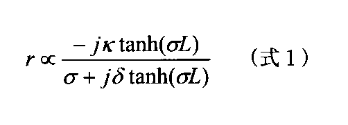
- j is an imaginary unit
- ⁇ is a coupling constant
- ⁇ 2 ⁇ 2 ⁇ 2
- L is the length of the grating.
- the angle of the light emitted from the grating of the optical coupler 114 with respect to the waveguide substrate is different from the angle of the light emitted from the grating of the light reflector 116 with respect to the waveguide substrate, but the reflection returns to the optical branch 110.
- the absolute value of the coefficient may be configured to be the same. With this configuration, the optical circuit 100 can clearly separate the light emitted from the grating of the optical coupler 114 and the light emitted from the grating of the optical reflector 116, and can suppress crosstalk of stray light. .
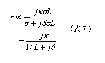
- the reflection coefficient of the optical coupler 114 and the reflection coefficient of the light reflection unit 116 as represented by Expression 1 have substantially the same absolute value of the reflection coefficient, but are different in phase from each other.
- the phase to the optical waveguide 112 ⁇ / b> A with respect to the waveguide on the modulator side is equal to the phase to the optical waveguide 112 ⁇ / b> B with respect to the waveguide on the modulator side, and the reflection coefficients of the optical coupler 114 and the light reflection unit 116 are absolute.
- the optical circuit 100 has an optical path length difference between the optical waveguides 112A and 112B of ((m ⁇ 1 / 2) ⁇ / ⁇ / 2. ) ⁇ / 2.
- the angle of the light emitted from the optical coupler 114 with respect to the waveguide substrate and the light emitted from the light reflecting portion 116 are increased.
- the angle with respect to the waveguide substrate is different, and the phase difference of the light reflected from the optical coupler 114 and the light reflector 116 and returned to the optical branch 110 via the optical waveguides 112A and 112B is (2m ⁇ ) in the optical branch 110.
- the optical circuit 100 can be realized such that ⁇ (m is an integer).
- the optical waveguides 112A and 112B are configured to have equal optical path lengths, and the phase of light reflected from the optical coupler 114 at the connection point between the optical waveguide 112A and the optical coupler 114 And the phase of the light reflected from the light reflecting portion 116 at the connection point between the optical waveguide 112B and the light reflecting portion 116 may be shifted by (2m ⁇ 1) ⁇ (m is an integer). .
- the phase of the reflection coefficient r expressed by Equation 1 is different by (2m ⁇ 1) ⁇ (m is an integer) between the grating of the optical coupler 114 and the grating of the light reflector 116.
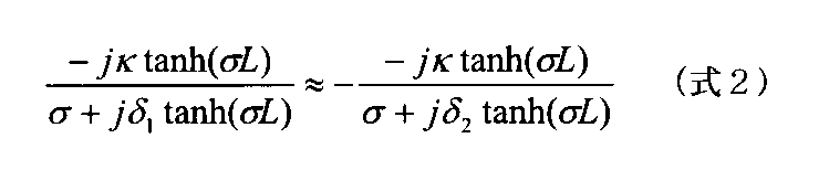
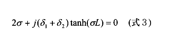
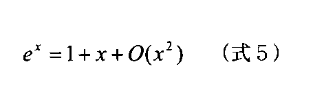
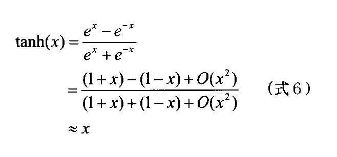
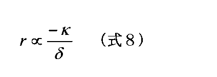
- the pitch ⁇ of each grating may be set. For example, in Equation 1, if ⁇ is equal and only the grating pitch is different and the phase of the reflection coefficient is shifted by ⁇ ,
- the optical coupler 114 and the light reflecting portion 116 are fabricated by the same manufacturing process. It is desirable to have the same structure.
- the optical coupler 114 and the light reflecting unit 116 are preferably configured as a grating coupler as in the above example.
- the above embodiment of the present invention has an advantageous effect. For example, when the edge emission type spot size conversion according to the prior art is applied to the light reflecting section 116, the end face is exposed by cleaving, dicing, or the like, so that the manufacturing error of the waveguide length increases.
- the grating coupler is used as the light reflecting portion 116 as in the embodiment of the present invention, the light reflecting portion 116 can be produced using an electron beam (EB). Increases accuracy. Further, if the grating couplers constituting the optical coupler 114 and the light reflecting portion 116 have exactly the same structure, they may not be configured with a uniform grating pitch.
- the optical waveguides 112A and 112B may have the same cross-sectional structure.
- the refractive index of the waveguide varies with temperature.
- the optical waveguides 112A and 112B may be arranged so as to be separated from each other by a distance that does not couple as a directional coupler and at a sufficiently close distance (for example, in parallel).
- the optical waveguides 112A and 112B are similarly subjected to a change in refractive index due to the influence of heat generated from an IC or a semiconductor laser.
- a change in refractive index due to the influence of heat generated from an IC or a semiconductor laser.
- only the difference in length between the optical waveguides 112A and 112B is affected by the temperature change.
- the optical path length of the optical waveguide 112A is L + ((m ⁇ 1 / 2) ⁇ ) / 2
- the optical path length of the optical waveguide 112B is L.
- the optical path length of the optical waveguide 112A is (1 + ⁇ ) (L + ((m ⁇ 1 / 2) ⁇ ) / 2), and the optical path of the optical waveguide 112B.
- the length is (1 + ⁇ ) L, and the difference between the optical path lengths of the two waveguides is (1 + ⁇ ) ((m ⁇ 1 / 2) ⁇ ) / 2.
- m is 1
- the optical path difference is (1 + ⁇ ) ⁇ / 4. Since ⁇ is small, the round-trip optical path difference is (1 + ⁇ ) ⁇ / 2 to ⁇ / 2, and the round-trip phase difference is held at ⁇ .
- the optical path length of the waveguide 112A is (1 + ⁇ ) (L + ((m ⁇ 1 / 2) ⁇ ) / 2), and the optical path length of the optical waveguide 112B.
- the difference between the optical path lengths of the two waveguides is ⁇ L + (1 + ⁇ ) ((m ⁇ 1 / 2) ⁇ ) / 2.
- the round-trip optical path difference is 2 ⁇ L + ⁇ / 2, and it is difficult to maintain the round-trip phase difference between the optical waveguides 112A and 112B at ⁇ . Therefore, by arranging the optical waveguides 112A and 112B so as to be separated from each other by a distance that is not coupled as a directional coupler and at a sufficiently close distance (for example, in parallel), the optical path difference between these waveguides is desired. It becomes easy to control so as to be held in the vicinity of the phase difference.
- the round-trip phase difference between the waveguides is ⁇ , but the present invention is not limited to this.
- the interval between the optical waveguide 112A and the optical waveguide 112B is desirably 50 ⁇ m or less.
- the optical waveguides 112A and 112B may be configured intentionally so that the respective cross-sectional structures are different and a desired phase difference is generated.
- the optical waveguides 112A and 112B may be configured to have the same length and different effective refractive indices.
- the optical waveguides 112A and 112B are arranged so that the phase difference of the light returned to the optical branch 110 via each of them is (2m ⁇ 1) ⁇ (m is an integer) in the optical branch 110.
- the refractive index can be configured to be different, or the core diameter can be configured to be different.
- FIG. 4 shows an optical circuit 400 according to another embodiment of the present invention. Similar to the optical circuit 100 shown in FIG. 1, the optical circuit 400 includes a light source 402, optical branches 404, 406A and 406B, optical modulators 408A, 408B, 408C and 408D, an optical branch 410, optical waveguides 412A and 412B, and optical coupling. And a light reflecting portion 416.
- the optical coupler 414 is configured to couple the light propagated through the optical waveguide 412A via the optical branch 410 to the optical waveguide 418 for transmission.
- the optical branch 410 is configured as a coupler (eg, 2 ⁇ 2 coupler) having at least two inputs and at least two outputs.
- the optical circuit 400 further includes an optical phase adjustment unit 420 on the optical waveguide 412B.
- the first input of the two inputs of the optical branch 410 is connected to the optical modulator 408A, and the second input is connected to a photodetector 422 such as a photodiode.
- the optical phase adjustment unit 420 may be configured as, for example, a MOS structure, a PN structure, a heater, or the like.
- MOS structure the phase of light propagating through the optical waveguide 412B is adjusted by applying a voltage to the optical phase adjustment unit 420.
- PN structure current is injected into the optical phase adjustment unit 420, and in the case of the heater, the optical phase adjustment unit 420 is heated.
- the optical power returning to the second input of the optical branch 410 is monitored by the photodetector 422. .
- the optical power detected by the photodetector 422 is maximized, the optical power returning from the first input of the optical branch 410 to the optical modulator 408A is minimized.
- the phase of the light reflected by the optical coupler 414 and returned to the first input of the optical branch 410 and the phase of the light reflected by the light reflector 416 and returned to the first input of the optical branch 410 are calculated.
- the phase difference between them is (2m ⁇ 1) ⁇ (m is an integer).
- the operation of the light source 402 can be stabilized by controlling the optical phase adjustment unit 420 so that the optical power detected by the photodetector 422 is maximized.
- the optical phase adjustment unit 420 and the photodetector 422 can be manufactured by the same process as other optical elements, and it is not necessary to increase the number of manufacturing steps.
- FIG. 5 shows an optical circuit 500 according to another embodiment of the present invention.
- the optical circuit 500 includes an optical phase adjusting unit 520A on the optical waveguide 512A in addition to the same configuration as the optical circuit 400 shown in FIG.
- the optical phase adjustment unit 520A is configured to have an optical loss equivalent to that of the optical phase adjustment unit 520B.
- the optical phase adjustment unit 520B is controlled so that the optical power detected by the photodetector 522 is maximized, while the optical phase adjustment unit 520A is not driven. According to the configuration of FIG.
- the optical loss in the optical waveguide 512A is equivalent to the optical loss in the optical waveguide 512B, so that the power of the light reflected by the optical coupler 514 and returned to the optical branch 510 and the light reflecting unit 510 The power of the light reflected and returned to the optical branch 510 becomes substantially equal. Therefore, by controlling the optical phase adjustment unit 520B so that the light detected by the photodetector 522 is maximized, the optical power returned from the optical branch 510 to the optical modulator 508A can be almost suppressed.
- the optical branches 410 and 510 equally divide the light from the modulator into two waveguides connected to the optical coupler from the viewpoint of suppressing manufacturing variations and maximizing the return light. It is desirable to be a thing. However, when the absolute values of the reflection coefficients of the designed light reflecting portions 416 and 516 are different from those of the optical couplers 414 and 514, the returning optical power is adjusted by changing the branching ratio of the optical branching by design. May be.
- FIG. 6 shows an optical circuit 600 according to another embodiment of the present invention. This is a modification of the optical circuit 400 of FIG.
- optical circuit 600 optical branch 610 has one input, and photodetector 622 is connected to one input of optical modulator 608A rather than the input of optical branch 610.
- the optical circuit 600 can stabilize the operation of the light source 602 by controlling the optical phase adjustment unit 620 so that the optical power detected by the photodetector 622 is minimized.
- the driving condition of the optical phase adjustment unit 620 that minimizes the optical power in the photodetector 622 may be determined directly.
- one driving condition of the optical phase adjusting unit 620 that maximizes the optical power in the photodetector 622 is determined, and further another driving condition of the optical phase adjusting unit 620 that maximizes the optical power is determined.
- the optical phase adjustment unit 620 may be driven using an intermediate value between these driving conditions.
- optical circuit 600 of FIG. 5 can also be configured such that the photodetector 522 is connected to one input of the optical modulator 508A as shown in FIG.
- another optical phase adjustment unit may be provided on the waveguide 612A as shown in FIG.
- an optical circuit can be manufactured at low cost. If an optical circuit is formed on an SOI (silicon on insulator) substrate using silicon photonics technology, an optical circuit having the above characteristics can be highly integrated on the substrate using a silicon process. Can be miniaturized, the manufacturing process can be simplified, and the manufacturing cost can be reduced.
- SOI silicon on insulator
- FIG. 7 shows an optical circuit 700 capable of reducing the instability of the operation of the light source due to the reflected light generated in the optical circuit after the optical modulator according to another embodiment of the present invention.
- the optical circuit 700 may be formed by integrating optical elements on an SOI substrate using silicon photonics technology.
- the configuration of the optical circuit connected to the output of the optical modulator 708A will be specifically described.
- similarly configured optical circuits may be connected to other optical modulators 708B, 708C, and 708D. .
- the optical circuit 700 is configured to branch the light output from the optical modulator 708A into two optical waveguides 712A and 712B via an optical branch 710.
- Optical waveguides 712A and 712B are connected to optical couplers 714A and 714B, respectively.
- FIG. 7 shows an example in which a grating coupler is used as the optical couplers 714A and 714B.
- the grating coupler includes a Si thin wire, a tapered waveguide connected to the Si thin wire, and a wide waveguide connected to the tapered waveguide and having a grating formed thereon.
- the core of the Si fine wire has, for example, a thickness of 60 nm and a width of 500 nm.
- the tapered waveguide has a length of, for example, 700 ⁇ m, widens the waveguide width of 500 nm to 10 ⁇ m, and is connected to the wide waveguide.
- the grating has, for example, a 635 nm period and a 50% duty cycle.
- the grating can be configured, for example, to have a thickness of 120 nm and an etching depth of 60 nm.
- an optical signal incident from a Si wire is spread by a tapered waveguide so as to have a spot size with a width of about 10 ⁇ m, diffracted by a grating (for example, upward), and directed to an optical waveguide such as an optical fiber.
- the grating couplers 714A and 714B are each configured to diffract part of the light branched by the optical branch 710 and couple it to the same optical waveguide 718 for transmission.
- the two grating couplers 714A and 714B are arranged to face each other, but the arrangement method is not limited.
- the grating couplers may be arranged in parallel as shown in FIG.
- the two grating couplers 714A and 714B are preferably in close proximity so that they can be coupled to the optical waveguide 718.
- the angle of the light emitted from the grating of the grating coupler 714A with respect to the waveguide substrate is different from the angle of the light emitted from the grating of the grating coupler 714B with respect to the waveguide substrate, but the reflection coefficient returns to the optical branch 710.
- the absolute value may be configured to be the same. For example, as shown in FIG. 12, when a grating is formed in a waveguide obliquely with respect to the waveguide, light is diffracted with respect to the oblique grating.
- the optical waveguide 718 may be an optical fiber.
- the optical waveguides 712A and 712B and the grating couplers 714A and 714B are configured such that the phase difference of the light reflected from the grating couplers 714A and 714B and returned to the optical branch 710 via the optical waveguides 712A and 712B is reduced on the light source side of the optical branch 710. It is configured to be (2m ⁇ 1) ⁇ (m is an integer).
- the phase to the optical waveguide 712A with respect to the modulator-side waveguide in the branch 710 and the optical waveguide 712B to the modulator-side waveguide The optical waveguides 712A and 712B have the same phase, and are configured so that the optical path length of the round trip differs by (m ⁇ 1 / 2) ⁇ (m is an integer, ⁇ is the wavelength of light emitted from the light source 402). Also good.
- the optical waveguides 712A and 712B are configured such that the one-way optical path lengths differ by ((m ⁇ 1 / 2) ⁇ ) / 2.
- the shift of the optical signal reflected from each of the grating couplers 714 and 716 is, for example, 1/100 in the optical branch 710. It is desirable to be less than a bit. In order to realize this, it is desirable that the difference in length between the optical waveguide 712A and the optical waveguide 712B is 1/100 or less of (c / ng) ⁇ (1 / k) (unit: m).
- ng is the group refractive index of the optical waveguides 712A and 712B
- c (m / s) is the speed of light
- k (bps) is the signal transmission speed.
- the optical circuit 700 has a phase difference between the light reflected from the grating coupler 714A and returned to the optical branch 710 and the light reflected from the grating coupler 714B and returned to the optical branch 710 at the optical branch 710 (2m ⁇ 1).
- the optical waveguides 712A and 712B may have different optical path lengths, and the grating coupler 714A and the grating coupler 714B may have different reflection coefficients so as to be ⁇ .
- the optical circuit 700 uses a 1 ⁇ 2 MMI and the phase to the optical waveguide 712A with respect to the modulator-side waveguide in the branch 710 is equal to the phase to the optical waveguide 712B with respect to the modulator-side waveguide.
- the difference between the phase of the reflection coefficient of the coupler 714A and the phase of the reflection coefficient of the grating coupler 714B is ⁇ , and the optical path length between the optical branch 710 and the grating coupler 714A and the optical branch 710 and the grating coupler 714B are configured.
- the difference between the optical path length and the optical path length is ((m ⁇ 1 / 2) ⁇ / ⁇ / 2) ⁇ / 2, m is an integer, and ⁇ is the wavelength of the optical signal. Good.
- a 2 ⁇ 2 multimode interference (MMI) optical coupler may be used in the optical branching unit used in the optical circuits 800 and 900 described later.
- the phase to the optical waveguide 712A with respect to the waveguide on the modulator side is different from the phase to the optical waveguide 712B with respect to the waveguide on the modulator side by ⁇ / 2. Therefore, for example, the difference between the phase of the reflection coefficient of the grating coupler 714A and the phase of the reflection coefficient of the grating coupler 714B is ⁇ , and the optical path length and the optical branch between the optical branch 710 and the grating coupler 714A are configured.
- the difference between the optical path length between 710 and the grating coupler 714B is (m ⁇ / ⁇ / 2) ⁇ / 2 in one way, m is an integer, and ⁇ is the wavelength of the optical signal. Also good. Also in this case, the phase difference between the reflected light from the grating coupler 714A and the reflected light from the grating coupler 714B is (2m-1) ⁇ (m is an integer) at the port where the light from the light source on the branching portion is incident. ). In view of manufacturing variations, it is desirable to use a 1 ⁇ 2 multimode interference (MMI) optical coupler rather than a 2 ⁇ 2 multimode interference (MMI) optical coupler. When the absolute value of the reflection coefficient is different between the optical couplers 714A and 714B, the returning optical power may be adjusted by changing the branching ratio of the optical branching by design.
- MMI multimode interference
- one grating may be formed obliquely with respect to the waveguide in the waveguide, and the other grating coupler may be disposed so as to be generally orthogonal to the waveguide.
- the grating couplers By arranging the grating couplers in parallel, the light from the grating coupler 1314A is diffracted and can be condensed by approaching the light of the grating coupler 1314B, and coupling from two separated grating couplers to one waveguide is possible. Becomes easy.
- the optical circuit 700 has a difference in optical path length between the optical waveguides 712A and 712B ( (M ⁇ 1 / 2) ⁇ / ⁇ / 2) ⁇ / 2 can be obtained.
- the angle of the light emitted from the grating coupler 714A with respect to the waveguide substrate is different from the angle of the light emitted from the grating coupler 714B with respect to the waveguide substrate, and the grating coupler 714A and the grating coupler 714B respectively.
- the branching ratio of the light branching 710 is preferably 1: 1.
- the reflection coefficient of the grating coupler 714A and the reflection coefficient of the grating coupler 714B are different from each other in the phase of the reflection coefficient by adjusting the grating pitch, grating depth, length L, coupling constant ⁇ , and duty ratio.
- the absolute values of the coefficients can be designed to be approximately equal. Return light can be reduced by making the absolute value of the reflection coefficient the same.
- the returning optical power can be adjusted by changing the branching ratio of the optical branching by design. Return light can be suppressed by coupling to the original waveguide with a phase difference ⁇ .
- the phase to the optical waveguide 712A with respect to the modulator-side waveguide in the branch 710 is equal to the phase to the optical waveguide 712B with respect to the modulator-side waveguide, and the optical waveguides 712A and 712B.
- the phase at the connection point with the coupler 714B may be shifted by (2m ⁇ 1) ⁇ (m is an integer).
- each grating is set such that the phase of the reflection coefficient r expressed by Equation 1 differs by (2m ⁇ 1) ⁇ (m is an integer) between the grating of the grating coupler 714A and the grating of the grating coupler 714B.
- the grating coupler 714A and the grating coupler 714B are configured in this way, the light reflected by the grating coupler 714A and the light reflected by the grating coupler 714B have substantially the same amplitude and a phase difference of ⁇ . Light can be canceled at the light branch 710.
- the reflection coefficient r may be adjusted by changing the depth, length L, coupling constant ⁇ , and duty ratio of the grating instead of changing the pitch of the grating.
- the grating coupler 714A and the grating coupler 714B can be manufactured by the same manufacturing process. Therefore, the reproducibility of the fabrication of the optical circuit 700 can be enhanced while achieving the effect of canceling the reflected light generated in the grating coupler.
- the optical waveguides 712A and 712B may have the same cross-sectional structure.
- the refractive index of the waveguide can vary with temperature.
- the optical waveguides 712A and 712B may be arranged so as to be separated from each other by a distance that is not coupled as a directional coupler and at a sufficiently close distance (for example, in parallel).
- the optical waveguides 712A and 712B are similarly subjected to a change in refractive index due to the influence of heat generated from an IC, a semiconductor laser, or the like.
- the difference between the lengths of the optical waveguides 712A and 712B is affected by the temperature change.
- the grating coupler 714 and the grating coupler 716 have the same reflection coefficient, and the reflection coefficient has the same absolute value and phase.
- the optical path length of the optical waveguide 712A is L + ((m ⁇ 1 / 2) ⁇ ) / 2
- the optical path length of the optical waveguide 712B is L.
- the optical path length of the optical waveguide 712A is (1 + ⁇ ) (L + ((m ⁇ 1 / 2) ⁇ ) / 2), and the optical waveguide 712B
- the optical path length is (1 + ⁇ ) L
- the difference between the optical path lengths of the two waveguides is (1 + ⁇ ) ((m ⁇ 1 / 2) ⁇ ) / 2.
- m 1, the optical path difference is (1 + ⁇ ) ⁇ / 4. Since ⁇ is small, the round trip optical path difference is (1 + ⁇ ) ⁇ / 2 to ⁇ / 2, and the round trip phase difference is held at ⁇ .
- the reciprocal phase difference between the waveguides is ⁇ .
- the distance between the optical waveguide 712A and the optical waveguide 712B is preferably 50 ⁇ m or less.
- the optical waveguides 712A and 712B may be intentionally configured so that the respective cross-sectional structures are different and a desired phase difference is generated.
- the optical waveguides 712A and 712B may be configured to have different effective refractive indices.
- the optical waveguides 712A and 712B are arranged so that the phase difference of the light returned to the optical branch 710 via each is (2m ⁇ 1) ⁇ (m is an integer) on the light source side of the optical branch 710. And it can comprise so that the refractive index of a clad may differ, or it may comprise so that a core diameter may differ.
- the optical circuit 700 of the present embodiment branches the light output from the optical modulator 708A into the two optical waveguides 712A and 712B by the optical branch 710, and further, the two optical waveguides 712A and 712B.
- the optical signal propagated by the optical fiber is coupled to one optical waveguide 718 again using two grating couplers 714A and 714B.
- the optical circuit 700 may be configured such that the optical signals diffracted by the grating couplers 714A and 714B are coupled to the same multimode optical waveguide 718, respectively.
- the multimode optical waveguide 718 may be, for example, a multimode optical fiber.
- the grating couplers 714A and 714B may be configured such that the spot size of light diffracted from each of them is within the core of the multimode optical waveguide 718 at the incident end of the multimode optical waveguide 718.
- the multimode optical waveguide 718 may be a multimode optical fiber having a core diameter of about 50 ⁇ m, and the grating couplers 714A and 714B have a spot size of light diffracted from each of about 10 ⁇ m. It may be configured.
- the optical signals diffracted from each of the grating couplers 714A and 714B can be made identical by simply placing the grating couplers 714A and 714B in close proximity and using no additional special optical element.
- the multimode optical waveguide 718 can be coupled. Therefore, the power of the optical signal coupled and transmitted to the optical waveguide 718 can be increased as compared with the embodiment of FIGS.
- the optical circuit 700 is configured to use a multimode optical waveguide 718 such as a multimode optical fiber as in this embodiment, the operation of the light source 702 is unstable due to reflection of light output from the optical modulator 708A.
- the optical modulator 708A In addition to reducing both the light diffracted from each of the grating couplers 714A and 714B into the same multimode optical waveguide 718, light resulting from intentional branching using the optical branch 710 Loss can be suppressed.
- the adverse effect of the reflected light from the optical element after the optical modulator 108A can be reduced, but the power of the optical signal coupled to the optical waveguide 118 is reduced by the optical branch 110 (for example, , 1 ⁇ 2).
- the problem of attenuation of the power of the optical signal can be solved at the same time.
- the optical circuit 700 can be manufactured at low cost. it can. If the optical circuit 700 is formed on an SOI substrate using silicon photonics technology, the optical circuit 700 having the above characteristics can be highly integrated on the substrate using a silicon process. Therefore, the optical circuit 700 can be downsized, the manufacturing process can be simplified, and the manufacturing cost can be reduced. Further, if a multimode optical waveguide is used as the optical signal transmission optical waveguide 718, the position between the optical circuit 700 and the optical waveguide 718 when the SOI circuit is highly integrated and miniaturized is reduced. Increased tolerance for alignment error.
- FIG. 8 schematically shows an optical circuit 800 according to another embodiment of the present invention.
- the optical branching unit 810 is configured as a coupler (eg, 2 ⁇ 2 coupler) having at least two inputs and at least two outputs.
- Light from modulator 808 is split in half by optical branch 810 and coupled to optical waveguides 812A and 812B.
- the optical circuit 800 further includes an optical phase adjustment unit 820 on the optical waveguide 812B.
- a first input of the two inputs of the optical branch 810 is connected to the optical modulator 808A, and a photodetector 822 such as a photodiode is connected to the other second input.
- the optical phase adjustment unit 820 may be, for example, a MOS structure, a PN structure, a heater, or the like.
- the power of the light returning to the second input among the return light to the optical branch 810 is monitored by the photodetector 822.
- the optical power detected by the photodetector 822 is maximized, the optical power returning from the first input of the optical branch 810 to the optical modulator 808A is minimized.
- the phase difference is (2m ⁇ 1) ⁇ (m is an integer).
- the operation of the light source 802 can be stabilized by controlling the optical phase adjustment unit 820 so that the optical power detected by the photodetector 822 is maximized.
- the optical phase adjustment unit 820 in addition to the effect of the optical circuit 700 shown in FIG. 7, even if manufacturing variations occur in the lengths of the optical waveguides 812A and 812B, the optical power returning to the optical modulator 808A is minimized. And the operation of the light source 802 can be further stabilized.
- FIG. 9 shows an optical circuit 900 according to another embodiment of the present invention.
- the optical circuit 900 includes an optical phase adjustment unit 920A on the optical waveguide 912A.
- the optical phase adjustment unit 920A is configured to have an optical loss equivalent to that of the optical phase adjustment unit 920B.
- the optical phase adjustment unit 920B is driven so that the optical power detected by the photodetector 922 is maximized, while the optical phase adjustment unit 920A is not driven.
- the optical loss in the optical waveguide 912A is equivalent to the optical loss in the optical waveguide 912B.
- the power of the light reflected by the grating coupler 914A and returned to the optical branch 910 is substantially equal to the power of the light reflected by the grating coupler 914B and returned to the optical branch 910, so that the light detected by the photodetector 922 is detected.
- the optical phase adjustment unit 920B By controlling the optical phase adjustment unit 920B so that becomes maximum, the optical power returned from the optical branching unit 910 to the optical modulator 908A can be minimized.
- FIG. 10 shows an optical circuit 1000 according to another embodiment of the present invention.
- the optical branch 1010 has one input, and the photodetector 1022 is connected to one input of the optical modulator 1008A.
- the optical circuit 1000 can stabilize the operation of the light source 1002 by controlling the optical phase adjustment unit 1020 so that the optical power detected by the photodetector 1022 is minimized.
- the driving condition of the optical phase adjustment unit 1020 that minimizes the optical power in the photodetector 1022 (for example, the applied voltage when the optical phase adjustment unit 1020 has a MOS structure) may be determined directly.
- one driving condition for the optical phase adjustment unit 1020 that maximizes the optical power in the photodetector 1022 is determined, and another driving condition for the optical phase adjustment unit 1020 that further maximizes the optical power is determined.
- the optical phase adjusting unit 1020 may be operated using an intermediate value between these driving conditions.
- the optical phase adjustment unit is formed only on the optical waveguide 1012B side, but from the viewpoint of adjusting the returning optical power, the optical phase adjustment unit is also formed on the optical waveguide 1012A side like the optical circuit 900. May be.
- the two grating couplers 814A and 814B, 914A and 914B, 1014A and 1014B have the same configuration from the viewpoint of suppressing manufacturing variation.
- the optical branching 810, 910, and 1010 may branch the light equally into two waveguides that connect the light from the modulator to the grating coupler from the viewpoint of maximizing the return light. desirable.
- the optical phase adjusting unit 820 is formed only on one side as in the optical circuit 800 and the absolute value of the optical power returning to the optical branching unit is different, the returning optical power is set to the optical branching ratio. You may adjust by changing by design.
- optical circuit 900 of FIG. 9 can also be configured such that the photodetector 922 is connected to one input of the optical modulator 908A as shown in FIG.
- another optical phase adjustment unit may be provided on the waveguide 1012A as shown in FIG.
- FIG. 11 schematically shows an optical circuit 1100 according to another embodiment of the present invention.
- the configuration after the optical modulators 1108A to 1108D is the same as that of the embodiment shown in FIG.
- the optical circuit 1100 has a difference between the phase of the reflected light from the optical modulators 1108A and 1108B and the phase of the reflected light from the optical modulators 1108C and 1108D before the light source 1102 (2m ⁇ 1) ⁇ .
- M is an integer).
- the optical waveguide between the optical modulators 1108A and 1108B and the light source 1102 and the optical waveguide between the optical modulators 1108C and 1108D and the light source 1102 have a reciprocal optical path length of (m ⁇ 1). / 2) ⁇ (m is an integer, ⁇ is the wavelength of light emitted from the light source 1102) may be different.
- ⁇ m is an integer, ⁇ is the wavelength of light emitted from the light source 1102
- the phase of the reflected light from the optical modulator 1108A and the phase of the reflected light from the optical modulator 1108B are (2m ⁇ 1) ⁇ (m is an integer) before the light source 1102, and the optical modulator 1108C
- the phase of the reflected light from the light source and the phase of the reflected light from the light modulator 1108D may be (2m ⁇ 1) ⁇ (m is an integer) before the light source 1102.
- the optical circuit 1100 has the phase of the reflected light from the optical modulator 1108A and the phase of the reflected light from the optical modulator 1108C become (2m ⁇ 1) ⁇ (m is an integer) before the light source 1102, and the optical modulation is performed.
- the phase of the reflected light from the optical device 1108B and the phase of the reflected light from the optical modulator 1108D may be (2m ⁇ 1) ⁇ (m is an integer) before the light source 1102.
- the optical path length can be expressed by multiplying the light propagation distance (d) by the effective refractive index (n) of the propagated light. Accordingly, the optical path length can be changed by changing the length of the linear portion of the waveguide by shifting the positional relationship of the optical element such as the branch element.
- the optical path length can be changed by changing the bending radius of the waveguide between the optical elements without changing the position of the optical elements.
- the waveguide may have a bent part of 90 °, for example, or may have another bending angle.
- various optical path lengths can be obtained by changing the effective refractive index by changing the width of the waveguide.
- each of the plurality of waveguides is affected by changing the height of the waveguide, changing the temperature of the waveguide, or covering the waveguide with one or more waveguides (for example, by applying a stressful film).
- Various optical path lengths can be obtained by changing the stress or changing the material of the waveguide core and cladding.
Landscapes
- Physics & Mathematics (AREA)
- General Physics & Mathematics (AREA)
- Optics & Photonics (AREA)
- Condensed Matter Physics & Semiconductors (AREA)
- Electromagnetism (AREA)
- Engineering & Computer Science (AREA)
- Microelectronics & Electronic Packaging (AREA)
- Optical Modulation, Optical Deflection, Nonlinear Optics, Optical Demodulation, Optical Logic Elements (AREA)
- Optical Integrated Circuits (AREA)
- Light Receiving Elements (AREA)
- Optical Couplings Of Light Guides (AREA)
Abstract
Description
Claims (18)
- 光を分岐する第1の分岐部と、
前記分岐された光のうちの第1の分岐光を伝送のために第1の光導波路に結合する第1の光結合器と、
前記分岐された光のうちの第2の分岐光を反射する光反射部と
を具備し、
前記第1の光結合器からの反射光と前記光反射部からの反射光との位相差が前記第1の分岐部の入力側において(2m-1)πであり、mは整数である光回路。 - 前記第1の分岐部及び前記第1の光結合器の間の第2の光導波路の長さと前記第1の分岐部及び前記光反射部の間の第3の光導波路の長さとの差が(c/ng)×(1/k)(単位:m)の100分の1以下であり、ngは前記第2の光導波路及び前記第3の光導波路の群屈折率、c(m/s)は光の速度、k(bps)は信号の伝送速度である請求項1に記載の光回路。
- 前記第1の分岐部は少なくとも2つの入力を有し、前記少なくとも2つの入力のうちの1つに光検出器が接続され、前記第3の光導波路上に第1の光位相調整部が設けられ、前記第1の光位相調整部は前記光検出器において検出される光パワーが最大となるように制御可能である請求項2に記載の光回路。
- 前記第2の光導波路上に第2の光位相調整部が設けられる請求項3に記載の光回路。
- 光源と、
前記光源から放射される光を変調して変調された光信号を出力する光変調器と
をさらに具備し、
前記光変調器は少なくとも2つの入力を有し、該少なくとも2つの入力のうちの1つに光検出器が接続され、前記光変調器の出力が前記第1の分岐部に接続され、前記第3の光導波路上に第1の光位相調整部が設けられ、前記第1の光位相調整部は前記光検出器において検出される光パワーが最小となるように制御可能である請求項2に記載の光回路。 - 前記第2の光導波路上に第2の光位相調整部が設けられる請求項5に記載の光回路。
- 前記光反射部は第2の光結合器であり、前記第1の光結合器からの反射光と前記第2の光結合器からの反射光とが前記第1の光導波路へ結合される請求項1乃至6のいずれか1項に記載の光回路。
- 前記第1の光結合器及び前記第2の光結合器はそれぞれ第1のグレーティングカプラ及び第2のグレーティングカプラであり、前記第1の光導波路はマルチモード光導波路である請求項7に記載の光回路。
- 前記光回路は同一の基板上に形成され、前記第1のグレーティングカプラ及び前記第2のグレーティングカプラは並行して配置され、前記第1のグレーティングカプラ及び前記第2のグレーティングカプラの前記基板に対する回折角は同じ角度であり互いに逆向きである請求項8に記載の光回路。
- 前記第1のグレーティングカプラ及び前記第2のグレーティングカプラは並行して配置され、前記第1のグレーティングカプラのグレーティングは前記第2の光導波路に対して斜めに形成され、前記第2のグレーティングカプラのグレーティングは前記第3の光導波路に対して直交するように形成され、前記第1のグレーティングカプラ及び前記第2のグレーティングカプラは反射係数の位相が互いに異なるが反射係数の絶対値がほぼ等しいように構成される請求項8に記載の光回路。
- 光源と、
前記光源から放射される光を分岐する第2の分岐部と、
前記第2の分岐部からの光の第1の部分を変調して、変調された光信号を出力する第1の光変調器と、
前記第2の分岐部からの光の第2の部分を変調して、変調された光信号を出力する第2の光変調器と
をさらに具備し、
前記第1の光変調器からの反射光と前記第2の光変調器からの反射光との位相差が前記第2の分岐部の入力側において(2m-1)πであり、mは整数である請求項1乃至4及び7乃至8のいずれか1項に記載の光回路。 - 前記光反射部は前記第1の光結合器と同一の反射係数を有する請求項1乃至11のいずれか1項に記載の光回路。
- 前記第1の光結合器の反射係数の位相と前記光反射部の反射係数の位相との間の差がφであり、前記第1の分岐部の入力側及び前記第1の光結合器の間の光路長と前記第1の分岐部の入力側及び前記光反射部の間の光路長との差分が((m-1/2)-φ/π/2)λ/2であり、mは整数であり、λは光の波長である請求項1乃至11のいずれか1項に記載の光回路。
- 前記第1の1x2構成の分岐部について入力に対し二つの出力側の間で位相差が生じない分岐構成で、前記第1の分岐部及び前記第1の光結合器の間の光路長と前記第1の分岐部及び前記光反射部の間の光路長とが等しく、前記第1の光結合器から反射される光の前記第1の光結合器の入射端における位相と前記光反射部から反射される光の前記光反射部の入射端における位相との間の位相差が(2m-1)πであり、mは整数である請求項1乃至11のいずれか1項に記載の光回路。
- 前記光回路は同一の基板上に形成され、前記第1の光結合器及び前記光反射部はそれぞれ第1のグレーティングカプラ及び第2のグレーティングカプラであり、前記第1のグレーティングカプラについてディチューニングδ=κであり、前記第2のグレーティングカプラについてδ=-κであるように、前記第1及び第2のグレーティングカプラのグレーティングピッチが決定され、ここで、κは結合定数であり、δ=β-Kであり、βは光の伝搬定数であり、K=2π/Λであり、Λはグレーティングピッチである請求項14に記載の光回路。
- 前記第2の分岐部から前記第1の光変調器までの第4の光導波路と、前記第2の分岐部から前記第2の光変調器までの第5の光導波路とは、方向性結合器として結合しない程度の距離だけ離れ且つ50μm以下の距離に並行に配置されることを特徴とする請求項11に記載の光回路。
- 前記第1の分岐部から前記第1の光結合器までの第2の光導波路と、前記第1の分岐部から前記光反射部までの第3の光導波路とは、方向性結合器として結合しない程度の距離だけ離れ且つ50μm以下の距離に並行に配置されることを特徴とする請求項1乃至16のいずれか1項に記載の光回路。
- 位相差は、
(a)光導波路の直線部の長さを変えること、
(b)光導波路の曲げ半径を変えること、
(c)光導波路の幅を変えること、
(d)光導波路の高さを変えること、
(e)光導波路の温度を変えること、
(f)光導波路にかかる応力を変えること、
(g)光導波路のコア又はクラッドの少なくとも1つの材料を変えること
の少なくとも1つによって光導波路の光路長を変えることによりもたらされる請求項1乃至17のいずれか1項に記載の光回路。
Priority Applications (3)
| Application Number | Priority Date | Filing Date | Title |
|---|---|---|---|
| US14/780,449 US9519115B2 (en) | 2013-03-25 | 2014-03-19 | Optical circuit |
| EP14773895.9A EP2980618B1 (en) | 2013-03-25 | 2014-03-19 | Optical circuit |
| JP2015508382A JP6422856B2 (ja) | 2013-03-25 | 2014-03-19 | 光回路 |
Applications Claiming Priority (2)
| Application Number | Priority Date | Filing Date | Title |
|---|---|---|---|
| JP2013062645 | 2013-03-25 | ||
| JP2013-062645 | 2013-03-25 |
Publications (1)
| Publication Number | Publication Date |
|---|---|
| WO2014156885A1 true WO2014156885A1 (ja) | 2014-10-02 |
Family
ID=51623864
Family Applications (1)
| Application Number | Title | Priority Date | Filing Date |
|---|---|---|---|
| PCT/JP2014/057541 Ceased WO2014156885A1 (ja) | 2013-03-25 | 2014-03-19 | 光回路 |
Country Status (4)
| Country | Link |
|---|---|
| US (1) | US9519115B2 (ja) |
| EP (1) | EP2980618B1 (ja) |
| JP (1) | JP6422856B2 (ja) |
| WO (1) | WO2014156885A1 (ja) |
Cited By (9)
| Publication number | Priority date | Publication date | Assignee | Title |
|---|---|---|---|---|
| JP2016191817A (ja) * | 2015-03-31 | 2016-11-10 | 日本電気株式会社 | 光集積回路、および光集積回路の制御方法 |
| JP2018054933A (ja) * | 2016-09-29 | 2018-04-05 | 沖電気工業株式会社 | 波長フィルタ |
| JP2018512626A (ja) * | 2015-03-12 | 2018-05-17 | メドルミクス, エセ.エレ.Medlumics, S.L. | 反射が抑制された双方向フォトニック集積回路 |
| US10228512B2 (en) | 2016-09-29 | 2019-03-12 | Oki Electric Industry Co., Ltd. | Wavelength filter |
| JP2019045749A (ja) * | 2017-09-05 | 2019-03-22 | 日本電信電話株式会社 | 光回路 |
| KR20200053520A (ko) * | 2017-09-21 | 2020-05-18 | 키옵티크 포토닉스 게엠베하 운트 콤파니 카게 | 다중 모드 공진 광 파라메트릭 발진기 기술에 기초하여 출력된 다중 세로 모드 연속파를 가진 광원 |
| KR20200118790A (ko) * | 2018-02-16 | 2020-10-16 | 아날로그 포토닉스, 엘엘씨 | 간섭을 통한 광학 위상 어레이 교정을 위한 시스템들, 방법들, 및 구조들 |
| CN113340808A (zh) * | 2020-03-02 | 2021-09-03 | 富士通光器件株式会社 | 光学装置和光学装置测试方法 |
| JP2025525645A (ja) * | 2022-07-25 | 2025-08-05 | 賽麗科技(蘇州)有限公司 | 光検出器、アレイ及び端末 |
Families Citing this family (26)
| Publication number | Priority date | Publication date | Assignee | Title |
|---|---|---|---|---|
| US11726332B2 (en) | 2009-04-27 | 2023-08-15 | Digilens Inc. | Diffractive projection apparatus |
| CN106125308B (zh) | 2012-04-25 | 2019-10-25 | 罗克韦尔柯林斯公司 | 用于显示图像的装置和方法 |
| JP6206409B2 (ja) * | 2012-08-29 | 2017-10-04 | 日本電気株式会社 | 光集積回路、および光集積回路における光デバイスの検査方法 |
| US9933684B2 (en) | 2012-11-16 | 2018-04-03 | Rockwell Collins, Inc. | Transparent waveguide display providing upper and lower fields of view having a specific light output aperture configuration |
| US10151865B2 (en) * | 2014-05-02 | 2018-12-11 | Futurewei Technologies, Inc. | Compact external grating PBS/PBC coupler |
| US9632226B2 (en) | 2015-02-12 | 2017-04-25 | Digilens Inc. | Waveguide grating device |
| US10690916B2 (en) | 2015-10-05 | 2020-06-23 | Digilens Inc. | Apparatus for providing waveguide displays with two-dimensional pupil expansion |
| CN108780224B (zh) * | 2016-03-24 | 2021-08-03 | 迪吉伦斯公司 | 用于提供偏振选择性全息波导装置的方法和设备 |
| EP3548939A4 (en) | 2016-12-02 | 2020-11-25 | DigiLens Inc. | UNIFORM OUTPUT LIGHTING WAVEGUIDE DEVICE |
| US10401655B2 (en) * | 2016-12-16 | 2019-09-03 | Elenion Technologies, Llc | Bias control of optical modulators |
| WO2018129398A1 (en) | 2017-01-05 | 2018-07-12 | Digilens, Inc. | Wearable heads up displays |
| US10514584B2 (en) | 2017-08-10 | 2019-12-24 | Sicoya Gmbh | Optical signal generator comprising a phase shifter |
| KR102745805B1 (ko) | 2018-01-08 | 2024-12-20 | 디지렌즈 인코포레이티드. | 광 도파관의 제조 방법 |
| US10732569B2 (en) | 2018-01-08 | 2020-08-04 | Digilens Inc. | Systems and methods for high-throughput recording of holographic gratings in waveguide cells |
| EP3710876A4 (en) | 2018-01-08 | 2022-02-09 | DigiLens Inc. | SYSTEMS AND PROCESSES FOR THE MANUFACTURE OF WAVEGUIDE CELLS |
| US20200225471A1 (en) | 2019-01-14 | 2020-07-16 | Digilens Inc. | Holographic Waveguide Display with Light Control Layer |
| GB2580607B (en) * | 2019-01-15 | 2021-11-17 | Gooch & Housego Torquay Ltd | Dual fibre optical apparatus |
| US20200247017A1 (en) | 2019-02-05 | 2020-08-06 | Digilens Inc. | Methods for Compensating for Optical Surface Nonuniformity |
| US20220283377A1 (en) | 2019-02-15 | 2022-09-08 | Digilens Inc. | Wide Angle Waveguide Display |
| JP2020181076A (ja) * | 2019-04-25 | 2020-11-05 | 日本電信電話株式会社 | 調芯用光回路および光調芯方法 |
| US20200386947A1 (en) | 2019-06-07 | 2020-12-10 | Digilens Inc. | Waveguides Incorporating Transmissive and Reflective Gratings and Related Methods of Manufacturing |
| US12099266B2 (en) * | 2019-06-24 | 2024-09-24 | Nippon Telegraph And Telephone Corporation | Optical circuit with common ground configuration for resistors and thermo-optic phase shifters |
| KR102775783B1 (ko) | 2019-08-29 | 2025-02-28 | 디지렌즈 인코포레이티드. | 진공 격자 및 이의 제조 방법 |
| US12253716B1 (en) * | 2019-10-15 | 2025-03-18 | Acacia Communications, Inc. | Photonic circuits with selectable number of input ports |
| CN118661138A (zh) | 2021-12-29 | 2024-09-17 | 迪吉伦斯公司 | 利用倒置母版进行全息记录的方法和系统 |
| CN119045118B (zh) * | 2024-09-23 | 2025-11-07 | 吉林大学 | 一种基于绝热耦合结构的薄膜铌酸锂与聚合物异质集成波导的光功率分配器及其制备方法 |
Citations (7)
| Publication number | Priority date | Publication date | Assignee | Title |
|---|---|---|---|---|
| JPH03259203A (ja) * | 1990-03-09 | 1991-11-19 | Sony Corp | 光導波路装置 |
| JPH09269428A (ja) * | 1996-03-29 | 1997-10-14 | Nec Corp | 反射戻り光補償回路 |
| JP2007047534A (ja) * | 2005-08-11 | 2007-02-22 | Ricoh Co Ltd | マルチビーム光源ユニット、光走査装置及び画像形成装置 |
| WO2008107963A1 (ja) | 2007-03-05 | 2008-09-12 | Fujitsu Limited | 光半導体素子 |
| JP2009204694A (ja) | 2008-02-26 | 2009-09-10 | Nec Corp | 波長フィルター及び、該波長フィルターを備えた光送信器 |
| US8168939B2 (en) | 2008-07-09 | 2012-05-01 | Luxtera, Inc. | Method and system for a light source assembly supporting direct coupling to an integrated circuit |
| JP2012133363A (ja) * | 2010-12-17 | 2012-07-12 | Samsung Electronics Co Ltd | 小型光変調器及びそれを含む光送信器 |
Family Cites Families (3)
| Publication number | Priority date | Publication date | Assignee | Title |
|---|---|---|---|---|
| US20030099420A1 (en) * | 2001-11-13 | 2003-05-29 | Achintya Bhowmik | Electro-optic modulator |
| JP5059601B2 (ja) * | 2004-04-15 | 2012-10-24 | インフィネラ コーポレイション | Wdm送信ネットワーク用クーラーレス集積回路および浮動波長グリッドフォトニック集積回路(pic) |
| EP2628038B1 (en) * | 2010-10-14 | 2020-02-19 | RWTH Aachen | Laser to chip coupler |
-
2014
- 2014-03-19 JP JP2015508382A patent/JP6422856B2/ja not_active Expired - Fee Related
- 2014-03-19 US US14/780,449 patent/US9519115B2/en not_active Expired - Fee Related
- 2014-03-19 WO PCT/JP2014/057541 patent/WO2014156885A1/ja not_active Ceased
- 2014-03-19 EP EP14773895.9A patent/EP2980618B1/en not_active Not-in-force
Patent Citations (7)
| Publication number | Priority date | Publication date | Assignee | Title |
|---|---|---|---|---|
| JPH03259203A (ja) * | 1990-03-09 | 1991-11-19 | Sony Corp | 光導波路装置 |
| JPH09269428A (ja) * | 1996-03-29 | 1997-10-14 | Nec Corp | 反射戻り光補償回路 |
| JP2007047534A (ja) * | 2005-08-11 | 2007-02-22 | Ricoh Co Ltd | マルチビーム光源ユニット、光走査装置及び画像形成装置 |
| WO2008107963A1 (ja) | 2007-03-05 | 2008-09-12 | Fujitsu Limited | 光半導体素子 |
| JP2009204694A (ja) | 2008-02-26 | 2009-09-10 | Nec Corp | 波長フィルター及び、該波長フィルターを備えた光送信器 |
| US8168939B2 (en) | 2008-07-09 | 2012-05-01 | Luxtera, Inc. | Method and system for a light source assembly supporting direct coupling to an integrated circuit |
| JP2012133363A (ja) * | 2010-12-17 | 2012-07-12 | Samsung Electronics Co Ltd | 小型光変調器及びそれを含む光送信器 |
Non-Patent Citations (1)
| Title |
|---|
| See also references of EP2980618A4 * |
Cited By (19)
| Publication number | Priority date | Publication date | Assignee | Title |
|---|---|---|---|---|
| JP2018512626A (ja) * | 2015-03-12 | 2018-05-17 | メドルミクス, エセ.エレ.Medlumics, S.L. | 反射が抑制された双方向フォトニック集積回路 |
| JP2016191817A (ja) * | 2015-03-31 | 2016-11-10 | 日本電気株式会社 | 光集積回路、および光集積回路の制御方法 |
| JP2018054933A (ja) * | 2016-09-29 | 2018-04-05 | 沖電気工業株式会社 | 波長フィルタ |
| US10228512B2 (en) | 2016-09-29 | 2019-03-12 | Oki Electric Industry Co., Ltd. | Wavelength filter |
| JP2019045749A (ja) * | 2017-09-05 | 2019-03-22 | 日本電信電話株式会社 | 光回路 |
| KR20200053520A (ko) * | 2017-09-21 | 2020-05-18 | 키옵티크 포토닉스 게엠베하 운트 콤파니 카게 | 다중 모드 공진 광 파라메트릭 발진기 기술에 기초하여 출력된 다중 세로 모드 연속파를 가진 광원 |
| KR102544583B1 (ko) * | 2017-09-21 | 2023-06-20 | 키옵티크 포토닉스 게엠베하 운트 콤파니 카게 | 다중 모드 공진 광 파라메트릭 발진기 기술에 기초하여 출력된 다중 세로 모드 연속파를 가진 광원 |
| KR102479006B1 (ko) * | 2018-02-16 | 2022-12-20 | 아날로그 포토닉스, 엘엘씨 | 간섭을 통한 광학 위상 어레이 교정을 위한 시스템들, 방법들, 및 구조들 |
| JP7165734B2 (ja) | 2018-02-16 | 2022-11-04 | アナログ フォトニクス エルエルシー | 光構造物とこれを較正する方法 |
| JP2022184848A (ja) * | 2018-02-16 | 2022-12-13 | アナログ フォトニクス エルエルシー | 光構造物 |
| JP2022184849A (ja) * | 2018-02-16 | 2022-12-13 | アナログ フォトニクス エルエルシー | 光構造物 |
| JP2021517656A (ja) * | 2018-02-16 | 2021-07-26 | アナログ フォトニクス エルエルシー | 光構造物とこれを較正する方法 |
| KR20200118790A (ko) * | 2018-02-16 | 2020-10-16 | 아날로그 포토닉스, 엘엘씨 | 간섭을 통한 광학 위상 어레이 교정을 위한 시스템들, 방법들, 및 구조들 |
| JP7324916B2 (ja) | 2018-02-16 | 2023-08-10 | アナログ フォトニクス エルエルシー | 光構造物 |
| JP7392066B2 (ja) | 2018-02-16 | 2023-12-05 | アナログ フォトニクス エルエルシー | 光構造物 |
| CN113340808A (zh) * | 2020-03-02 | 2021-09-03 | 富士通光器件株式会社 | 光学装置和光学装置测试方法 |
| CN113340808B (zh) * | 2020-03-02 | 2023-10-10 | 富士通光器件株式会社 | 光学装置和光学装置测试方法 |
| JP2025525645A (ja) * | 2022-07-25 | 2025-08-05 | 賽麗科技(蘇州)有限公司 | 光検出器、アレイ及び端末 |
| JP7901392B2 (ja) | 2022-07-25 | 2026-08-06 | シリス テクノロジー プライベート リミテッド | 光検出器、アレイ及び端末 |
Also Published As
| Publication number | Publication date |
|---|---|
| EP2980618B1 (en) | 2018-07-04 |
| US20160054529A1 (en) | 2016-02-25 |
| US9519115B2 (en) | 2016-12-13 |
| EP2980618A4 (en) | 2016-12-07 |
| JP6422856B2 (ja) | 2018-11-14 |
| JPWO2014156885A1 (ja) | 2017-02-16 |
| EP2980618A1 (en) | 2016-02-03 |
Similar Documents
| Publication | Publication Date | Title |
|---|---|---|
| JP6422856B2 (ja) | 光回路 | |
| US12313885B2 (en) | Photonics grating coupler and method of manufacture | |
| US10236985B2 (en) | Method and system for silicon photonics wavelength division multiplexing transceivers | |
| US9620931B2 (en) | Optical device, optical transmission device, optical reception device, hybrid laser and optical transmission apparatus | |
| JP6089077B1 (ja) | 導波路型光回折格子及び光波長フィルタ | |
| KR101333418B1 (ko) | 광학 디바이스, 광학 디바이스 사용 방법 및 광학 디바이스 제조 방법 | |
| JP6200642B2 (ja) | 光学装置 | |
| US11143816B2 (en) | Method and system for stabilized directional couplers | |
| US20160116680A1 (en) | Light coupling structure and optical device including a grating coupler | |
| CN101952753B (zh) | 光波导元件、波长色散补偿元件及其设计方法、滤光器及其设计方法、以及光谐振器及其设计方法 | |
| US10444429B1 (en) | Single edge coupling of chips with integrated waveguides | |
| JP6771602B2 (ja) | 波長制御素子及び波長制御方法 | |
| WO2010007888A1 (ja) | 光波長合分波回路 | |
| JP6402519B2 (ja) | 光導波路素子 | |
| US9151901B2 (en) | Wavelength-selective path-switching element | |
| JP6127171B1 (ja) | 偏波無依存波長フィルタ | |
| CN115398296B (zh) | 具有包括集成控制装置的相控阵天线的光电发射器 | |
| US9933576B2 (en) | Electro-optic device with an optical grating coupler having a grating period variation and methods of formation thereof | |
| US20250028218A1 (en) | Optoelectronic emitter having a phase-controlled antenna array comprising optical antennas suitable for emitting light radiation according to a predefined emission profile and in a predefined direction | |
| JP6109002B2 (ja) | 光導波素子 | |
| JP2012047852A (ja) | 光結合構造、光回路、および光結合方法 |
Legal Events
| Date | Code | Title | Description |
|---|---|---|---|
| 121 | Ep: the epo has been informed by wipo that ep was designated in this application |
Ref document number: 14773895 Country of ref document: EP Kind code of ref document: A1 |
|
| ENP | Entry into the national phase |
Ref document number: 2015508382 Country of ref document: JP Kind code of ref document: A |
|
| NENP | Non-entry into the national phase |
Ref country code: DE |
|
| WWE | Wipo information: entry into national phase |
Ref document number: 14780449 Country of ref document: US |
|
| WWE | Wipo information: entry into national phase |
Ref document number: 2014773895 Country of ref document: EP |