WO2014157619A1 - 有機エレクトロルミネッセンス素子 - Google Patents
有機エレクトロルミネッセンス素子 Download PDFInfo
- Publication number
- WO2014157619A1 WO2014157619A1 PCT/JP2014/059121 JP2014059121W WO2014157619A1 WO 2014157619 A1 WO2014157619 A1 WO 2014157619A1 JP 2014059121 W JP2014059121 W JP 2014059121W WO 2014157619 A1 WO2014157619 A1 WO 2014157619A1
- Authority
- WO
- WIPO (PCT)
- Prior art keywords
- light emitting
- emitting material
- layer
- light
- organic electroluminescence
- Prior art date
- Legal status (The legal status is an assumption and is not a legal conclusion. Google has not performed a legal analysis and makes no representation as to the accuracy of the status listed.)
- Ceased
Links
Images


Classifications
-
- H—ELECTRICITY
- H10—SEMICONDUCTOR DEVICES; ELECTRIC SOLID-STATE DEVICES NOT OTHERWISE PROVIDED FOR
- H10K—ORGANIC ELECTRIC SOLID-STATE DEVICES
- H10K50/00—Organic light-emitting devices
- H10K50/10—OLEDs or polymer light-emitting diodes [PLED]
- H10K50/11—OLEDs or polymer light-emitting diodes [PLED] characterised by the electroluminescent [EL] layers
- H10K50/12—OLEDs or polymer light-emitting diodes [PLED] characterised by the electroluminescent [EL] layers comprising dopants
- H10K50/121—OLEDs or polymer light-emitting diodes [PLED] characterised by the electroluminescent [EL] layers comprising dopants for assisting energy transfer, e.g. sensitization
-
- H—ELECTRICITY
- H10—SEMICONDUCTOR DEVICES; ELECTRIC SOLID-STATE DEVICES NOT OTHERWISE PROVIDED FOR
- H10K—ORGANIC ELECTRIC SOLID-STATE DEVICES
- H10K50/00—Organic light-emitting devices
- H10K50/10—OLEDs or polymer light-emitting diodes [PLED]
- H10K50/11—OLEDs or polymer light-emitting diodes [PLED] characterised by the electroluminescent [EL] layers
- H10K50/125—OLEDs or polymer light-emitting diodes [PLED] characterised by the electroluminescent [EL] layers specially adapted for multicolour light emission, e.g. for emitting white light
- H10K50/13—OLEDs or polymer light-emitting diodes [PLED] characterised by the electroluminescent [EL] layers specially adapted for multicolour light emission, e.g. for emitting white light comprising stacked EL layers within one EL unit
-
- H—ELECTRICITY
- H10—SEMICONDUCTOR DEVICES; ELECTRIC SOLID-STATE DEVICES NOT OTHERWISE PROVIDED FOR
- H10K—ORGANIC ELECTRIC SOLID-STATE DEVICES
- H10K2101/00—Properties of the organic materials covered by group H10K85/00
- H10K2101/20—Delayed fluorescence emission
-
- H—ELECTRICITY
- H10—SEMICONDUCTOR DEVICES; ELECTRIC SOLID-STATE DEVICES NOT OTHERWISE PROVIDED FOR
- H10K—ORGANIC ELECTRIC SOLID-STATE DEVICES
- H10K50/00—Organic light-emitting devices
- H10K50/10—OLEDs or polymer light-emitting diodes [PLED]
- H10K50/11—OLEDs or polymer light-emitting diodes [PLED] characterised by the electroluminescent [EL] layers
- H10K50/12—OLEDs or polymer light-emitting diodes [PLED] characterised by the electroluminescent [EL] layers comprising dopants
-
- H—ELECTRICITY
- H10—SEMICONDUCTOR DEVICES; ELECTRIC SOLID-STATE DEVICES NOT OTHERWISE PROVIDED FOR
- H10K—ORGANIC ELECTRIC SOLID-STATE DEVICES
- H10K50/00—Organic light-emitting devices
- H10K50/10—OLEDs or polymer light-emitting diodes [PLED]
- H10K50/14—Carrier transporting layers
- H10K50/15—Hole transporting layers
-
- H—ELECTRICITY
- H10—SEMICONDUCTOR DEVICES; ELECTRIC SOLID-STATE DEVICES NOT OTHERWISE PROVIDED FOR
- H10K—ORGANIC ELECTRIC SOLID-STATE DEVICES
- H10K50/00—Organic light-emitting devices
- H10K50/10—OLEDs or polymer light-emitting diodes [PLED]
- H10K50/14—Carrier transporting layers
- H10K50/16—Electron transporting layers
-
- H—ELECTRICITY
- H10—SEMICONDUCTOR DEVICES; ELECTRIC SOLID-STATE DEVICES NOT OTHERWISE PROVIDED FOR
- H10K—ORGANIC ELECTRIC SOLID-STATE DEVICES
- H10K50/00—Organic light-emitting devices
- H10K50/10—OLEDs or polymer light-emitting diodes [PLED]
- H10K50/17—Carrier injection layers
-
- H—ELECTRICITY
- H10—SEMICONDUCTOR DEVICES; ELECTRIC SOLID-STATE DEVICES NOT OTHERWISE PROVIDED FOR
- H10K—ORGANIC ELECTRIC SOLID-STATE DEVICES
- H10K50/00—Organic light-emitting devices
- H10K50/10—OLEDs or polymer light-emitting diodes [PLED]
- H10K50/17—Carrier injection layers
- H10K50/171—Electron injection layers
-
- H—ELECTRICITY
- H10—SEMICONDUCTOR DEVICES; ELECTRIC SOLID-STATE DEVICES NOT OTHERWISE PROVIDED FOR
- H10K—ORGANIC ELECTRIC SOLID-STATE DEVICES
- H10K50/00—Organic light-emitting devices
- H10K50/10—OLEDs or polymer light-emitting diodes [PLED]
- H10K50/18—Carrier blocking layers
-
- H—ELECTRICITY
- H10—SEMICONDUCTOR DEVICES; ELECTRIC SOLID-STATE DEVICES NOT OTHERWISE PROVIDED FOR
- H10K—ORGANIC ELECTRIC SOLID-STATE DEVICES
- H10K85/00—Organic materials used in the body or electrodes of devices covered by this subclass
- H10K85/60—Organic compounds having low molecular weight
- H10K85/615—Polycyclic condensed aromatic hydrocarbons, e.g. anthracene
- H10K85/626—Polycyclic condensed aromatic hydrocarbons, e.g. anthracene containing more than one polycyclic condensed aromatic rings, e.g. bis-anthracene
-
- H—ELECTRICITY
- H10—SEMICONDUCTOR DEVICES; ELECTRIC SOLID-STATE DEVICES NOT OTHERWISE PROVIDED FOR
- H10K—ORGANIC ELECTRIC SOLID-STATE DEVICES
- H10K85/00—Organic materials used in the body or electrodes of devices covered by this subclass
- H10K85/60—Organic compounds having low molecular weight
- H10K85/631—Amine compounds having at least two aryl rest on at least one amine-nitrogen atom, e.g. triphenylamine
- H10K85/633—Amine compounds having at least two aryl rest on at least one amine-nitrogen atom, e.g. triphenylamine comprising polycyclic condensed aromatic hydrocarbons as substituents on the nitrogen atom
-
- H—ELECTRICITY
- H10—SEMICONDUCTOR DEVICES; ELECTRIC SOLID-STATE DEVICES NOT OTHERWISE PROVIDED FOR
- H10K—ORGANIC ELECTRIC SOLID-STATE DEVICES
- H10K85/00—Organic materials used in the body or electrodes of devices covered by this subclass
- H10K85/60—Organic compounds having low molecular weight
- H10K85/649—Aromatic compounds comprising a hetero atom
- H10K85/654—Aromatic compounds comprising a hetero atom comprising only nitrogen as heteroatom
-
- H—ELECTRICITY
- H10—SEMICONDUCTOR DEVICES; ELECTRIC SOLID-STATE DEVICES NOT OTHERWISE PROVIDED FOR
- H10K—ORGANIC ELECTRIC SOLID-STATE DEVICES
- H10K85/00—Organic materials used in the body or electrodes of devices covered by this subclass
- H10K85/60—Organic compounds having low molecular weight
- H10K85/649—Aromatic compounds comprising a hetero atom
- H10K85/657—Polycyclic condensed heteroaromatic hydrocarbons
- H10K85/6572—Polycyclic condensed heteroaromatic hydrocarbons comprising only nitrogen in the heteroaromatic polycondensed ring system, e.g. phenanthroline or carbazole
-
- H—ELECTRICITY
- H10—SEMICONDUCTOR DEVICES; ELECTRIC SOLID-STATE DEVICES NOT OTHERWISE PROVIDED FOR
- H10K—ORGANIC ELECTRIC SOLID-STATE DEVICES
- H10K85/00—Organic materials used in the body or electrodes of devices covered by this subclass
- H10K85/60—Organic compounds having low molecular weight
- H10K85/649—Aromatic compounds comprising a hetero atom
- H10K85/657—Polycyclic condensed heteroaromatic hydrocarbons
- H10K85/6576—Polycyclic condensed heteroaromatic hydrocarbons comprising only sulfur in the heteroaromatic polycondensed ring system, e.g. benzothiophene
Definitions
- the present invention relates to a multi-wavelength light emitting type organic electroluminescence element.
- organic electroluminescent elements having a structure in which a cathode, an anode, and a light-emitting layer containing a light-emitting material are formed between the anode and the cathode has been actively conducted. Most of them are intended to develop a monochromatic organic electroluminescence device by incorporating a single light emitting material having a specific light emission wavelength into a light emitting layer. Among them, there are a plurality of light emitting materials having different light emission wavelengths. Some have aimed to develop a multi-wavelength light-emitting organic electroluminescence device using the above.
- a light emitting layer containing a blue light emitting material, a light emitting layer containing a green light emitting material, and a light emitting layer containing a red light emitting material are formed, and light emission from each light emitting material is mixed to achieve white light emission.
- Cited Document 1 has a light emitting layer containing a blue or blue-green fluorescent light emitting material and a light emitting layer containing a phosphorescent light emitting material other than blue, and the lowest excited triplet energy level of the fluorescent light emitting material is phosphorescent.
- An organic electroluminescent device is described which is characterized by being greater than the lowest excited triplet energy level of the luminescent material.
- an organic electroluminescence device in which an anode, a hole transport layer, a hole side mediating layer, an orange-red light emitting layer, a blue light emitting layer, a green light emitting layer, an electron side mediating layer, an electron transport layer, and a cathode are formed in this order. Is described.
- Cited Document 2 a green light emitting layer containing a green delayed fluorescent material is formed in the light emitting layer so as to be in contact with the hole transport layer, a red phosphorescent light emitting layer containing a red light emitting material is formed so as to be in contact with the green light emitting layer, Furthermore, an organic electroluminescence element is described in which a blue light emitting layer containing a blue light emitting material is formed so as to be in contact with the red light emitting layer.
- This organic electroluminescence device is designed so that the HOMO of the green delayed fluorescent material is deeper than the HOMO of the material of the hole transport layer and shallower than the HOMO of the red phosphorescent material.
- the organic electroluminescence element described in Patent Document 1 has a problem that the blue fluorescence intensity is insufficient because the internal quantum efficiency of blue fluorescence from the blue fluorescent material cannot be more than 25%. . Since this is a theoretical limit value, the problem cannot be solved as long as the configuration of Patent Document 1 is adopted.
- the organic electroluminescence element described in Patent Document 2 it is possible to improve the luminous efficiency of red phosphorescence, but nothing about effectively increasing the luminous efficiency of short wavelengths such as blue. No suggestion has been made.
- the present inventors have found that a multi-wavelength light-emitting organic electroluminescence device can be provided by using delayed fluorescence so as to satisfy specific conditions.
- the organic electroluminescence element developed by the present inventors is based on an unprecedented technical idea, and has a high degree of freedom in design, and is therefore highly practical. Based on these findings, the present inventors have provided the following present invention as means for solving the above problems.
- a multi-wavelength light emitting organic electroluminescence which has a cathode, an anode, and at least one organic layer containing a plurality of light emitting materials between the cathode and the anode, and emits light from the plurality of light emitting materials.
- An organic electroluminescence device which is an element, and the light having the shortest wavelength among the light emitted from the light emitting material includes delayed fluorescence.
- the energy difference ( ⁇ E ST ) between the lowest excited triplet energy level of 5K and the lowest excited singlet energy level ( ⁇ E ST ) of the light emitting material that emits light at the shortest wavelength is 0.3 eV or less
- the organic electroluminescent element according to any one of [1] to [3], wherein the light emitting material that emits light at the shortest wavelength is a blue light emitting material.
- a light-emitting material that emits light at the shortest wavelength and at least one light-emitting material that emits light at other wavelengths are included in one organic layer, and the light-emitting material that emits light at the shortest wavelength can be used as a host material.
- a light emitting material that emits light at the shortest wavelength and at least two kinds of light emitting materials that emit light at other wavelengths are included in one organic layer, and the light emitting material that emits light at the shortest wavelength is the host material.
- the organic electroluminescent device according to any one of [1] to [7], wherein the light emitting material that emits light at the shortest wavelength independently forms at least one organic layer. .
- Two or more layers containing a light emitting material are formed, and the layer closest to the cathode and the layer closest to the anode are both layers containing a light emitting material that emits light at the shortest wavelength.
- the organic electroluminescence device according to any one of [8].
- the organic electroluminescence device according to any one of [1] to [10], wherein the blue light-emitting material includes a layer doped with a green light-emitting material or a red light-emitting material.
- a layer containing a blue light emitting material, a layer obtained by laminating a layer containing a blue light emitting material doped with a green light emitting material or a red light emitting material, and a layer containing a blue light emitting material [1] to [10] Organic electroluminescent element of any one of these.
- the organic electroluminescence element according to any one of [1] to [12], wherein the plurality of light emitting materials include a blue light emitting material, a green light emitting material, and a red light emitting material.
- the blue light-emitting material includes a layer doped with a green light-emitting material and a red light-emitting material.
- the organic electroluminescent element of the item [16] The organic electroluminescence device according to any one of [1] to [15], wherein all of the plurality of light emitting materials emit delayed fluorescence. [17] The organic electroluminescent element according to any one of [1] to [15], wherein at least one of the plurality of light emitting materials emits phosphorescence. [18] The organic electroluminescence device as described in any one of [1] to [17], wherein light emitted from the plurality of light emitting materials is mixed to emit white light.
- the light emitting material that emits light having the shortest wavelength also emits delayed fluorescence. For this reason, the efficiency of light emission with a short wavelength such as blue can be increased and the color can be improved. Further, the organic electroluminescence device of the present invention has a high degree of design freedom, and a desired multi-wavelength light-emitting organic electroluminescence device can be produced with a simple structure.
- FIG. 2 is an emission spectrum of the organic electroluminescence element of Example 1.
- FIG. 3 is a current density-external quantum efficiency characteristic of the organic electroluminescent element of Example 1.
- FIG. 2 is an energy band diagram of the organic electroluminescence element of Example 1.
- 2 is an emission spectrum of organic electroluminescence elements of Examples 2 to 4.
- FIG. 6 is a graph showing current density-external quantum efficiency characteristics of organic electroluminescent elements of Examples 2 to 4.
- FIG. 5 is an energy band diagram of organic electroluminescence elements of Examples 2 to 4. 6 is an emission spectrum of the organic electroluminescence element of Example 5.
- FIG. 5 is an energy band diagram of organic electroluminescence elements of Examples 2 to 4. 6 is an emission spectrum of the organic electroluminescence element of Example 5.
- FIG. 10 is a current density-external quantum efficiency characteristic of the organic electroluminescent element of Example 5.
- FIG. FIG. 6 is an energy band diagram of the organic electroluminescence element of Example 5.
- 7 is an emission spectrum of the organic electroluminescent element A of Example 6.
- 6 shows voltage-current density characteristics of organic electroluminescent elements A to C of Examples 6 to 8. This is the current density-external quantum efficiency characteristics of the organic electroluminescent elements A to C of Examples 6 to 8.
- FIG. 6 is an energy band diagram of organic electroluminescence elements of Examples 6 to 8.
- FIG. 6 is an emission spectrum of organic electroluminescent elements D to F in Examples 9 to 11.
- FIG. This is a voltage-current density characteristic of the organic electroluminescent elements D to F of Examples 9 to 11. This is the current density-external quantum efficiency characteristics of the organic electroluminescent elements D to F of Examples 9 to 11.
- a numerical range represented by using “to” means a range including numerical values described before and after “to” as a lower limit value and an upper limit value.
- the multi-wavelength light-emitting organic electroluminescence element of the present invention includes at least a cathode, an anode, and an organic layer sandwiched between them. It is sufficient that at least one organic layer is formed, and a plurality of light emitting materials are included in the organic layer. At this time, the plurality of light emitting materials may be included in different organic layers, or may be included in the same organic layer. For example, in the case of using three kinds of light emitting materials of a blue light emitting material, a green light emitting material, and a red light emitting material, these three kinds of light emitting materials may be included in one light emitting layer, or each of the three organic layers. May be included.
- a specific light emitting material may be included in a plurality of organic layers.
- these light emitting materials each emit light and function as a multi-wavelength light emitting type.
- a light emitting material having a maximum emission wavelength of 400 nm or more and 490 nm or less is a blue light emitting material
- a light emitting material having a maximum emission wavelength of more than 490 nm and less than 580 nm is a green light emitting material
- a maximum is more than 580 nm and less than 700 nm.
- a light emitting material having an emission wavelength is a red light emitting material.
- the light having the shortest wavelength among the light emitted from the light emitting material contained in the device contains delayed fluorescence.
- delayed fluorescence can be emitted by selecting a delayed fluorescent material (delayed phosphor) that emits delayed fluorescence as a light emitting material and using it in an organic electroluminescence element. If such a delayed fluorescent material is used, the luminous efficiency of the fluorescent wavelength of the delayed fluorescent material can be increased. The principle is explained as follows.
- an organic electroluminescence element carriers are injected into a light emitting material from both positive and negative electrodes to generate an excited light emitting material and emit light.
- 25% of the generated excitons are excited to the excited singlet state, and the remaining 75% are excited to the excited triplet state. Therefore, the use efficiency of energy is higher when phosphorescence, which is light emission from an excited triplet state, is used.
- the excited triplet state has a long lifetime, energy saturation occurs due to saturation of the excited state and interaction with excitons in the excited triplet state, and in general, the quantum yield of phosphorescence is often not high.
- delayed fluorescent materials after energy transition to an excited triplet state due to intersystem crossing, etc., are then crossed back to an excited singlet state due to triplet-triplet annihilation or absorption of thermal energy, and emit fluorescence.
- a thermally activated delayed fluorescent material by absorption of thermal energy is particularly useful.
- excitons in the excited singlet state emit fluorescence as usual.
- excitons in the excited triplet state absorb heat generated by the device and cross between the excited singlets to emit fluorescence.
- the light is emitted from the excited singlet, the light is emitted at the same wavelength as the fluorescence, but the light lifetime (luminescence lifetime) generated by the reverse intersystem crossing from the excited triplet state to the excited singlet state is normal. Since the fluorescence becomes longer than the fluorescence and phosphorescence, it is observed as fluorescence delayed from these. This can be defined as delayed fluorescence. If such a heat-activated exciton transfer mechanism is used, the ratio of the compound in an excited singlet state, which normally generated only 25%, is increased to 25% or more by absorbing thermal energy after carrier injection. It can be raised.
- the energy difference ( ⁇ E ST ) between the lowest excited triplet energy level at 77 ° K and the lowest excited singlet energy level ( ⁇ E ST ) of the delayed fluorescent material is preferably 0.2 eV or less, more preferably 0.1 eV or less. preferable.
- the light emitting material having the shortest emission wavelength is selected as a light emitting material that emits such delayed fluorescence.
- This not only dramatically improves the light emission efficiency of the emission wavelength, but also moves the excited triplet state excitons to the excited triplet state of other long wavelength light emitting materials as shown in FIG.
- the luminous efficiency of other light emitting materials can be improved.
- Phosphorescence may be emitted from other light emitting materials, fluorescence may be emitted, or delayed fluorescence may be emitted when the other light emitting materials are also delayed fluorescent materials. If a delayed fluorescent material is selected as the other light emitting material, the luminous efficiency of the other light emitting material can be dramatically improved by the same mechanism as described above.
- FIG. 1 is a diagram illustrating, as an example, an embodiment using three light emitting materials of a blue light emitting material, a green light emitting material, and a red light emitting material.
- the blue light emitting material which is the light emitting material having the shortest wavelength only needs to be the delayed fluorescent material.
- the green light emitting material and the red light emitting material may be ordinary phosphorescent light emitting materials, one of which may be a delayed fluorescent material and the other may be a phosphorescent light emitting material.
- blue delayed fluorescent light (TADF) is emitted together with normal blue fluorescent light (Fluo), and the blue light emitting efficiency is dramatically improved.
- excitons in the excited triplet state of the blue light-emitting material move to the excited triplet state of the green light-emitting material and the excited triplet state of the red light-emitting material, and these emit phosphorescence and delayed fluorescence, respectively.
- Blue light emission, green light emission, and red light emission are mixed and recognized as white light emission.
- the type of delayed fluorescent material that can be used in the present invention is not particularly limited. It can be selected in consideration of the emission wavelength from those that can emit delayed fluorescence.
- the delayed fluorescent material generally has a structure in which an acceptor site (A) and a donor site (D) are bonded.
- the number of acceptor sites and donor sites may be one or more, and the number of acceptor sites and the number of donor sites in one molecule may or may not match.
- there are delayed fluorescent materials having various structural patterns such as AD type, A- (D) n type, (A) nD type, and-(AD) n-type (n is 2). Represents the above integer, for example, any one of 2 to 6).
- the molecular weight of the delayed fluorescent material is preferably 1500 or less, more preferably 1200 or less, and more preferably 1000 or less when the light-emitting layer is intended to be formed by vapor deposition. More preferably, it is still more preferably 800 or less.
- the delayed fluorescent material can be formed by a coating method regardless of the molecular weight. If a coating method is used, a film can be formed even with a compound having a relatively large molecular weight.
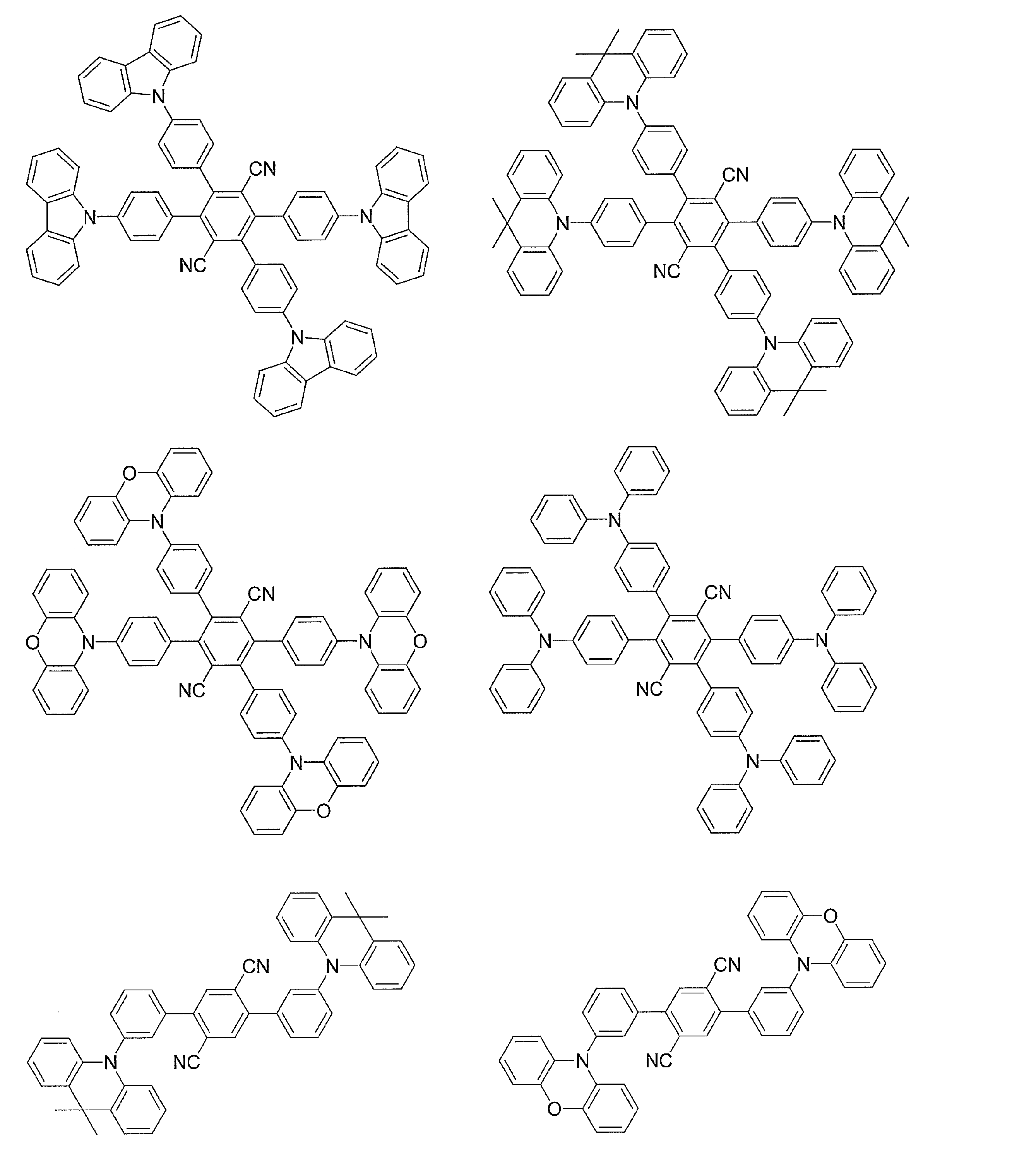
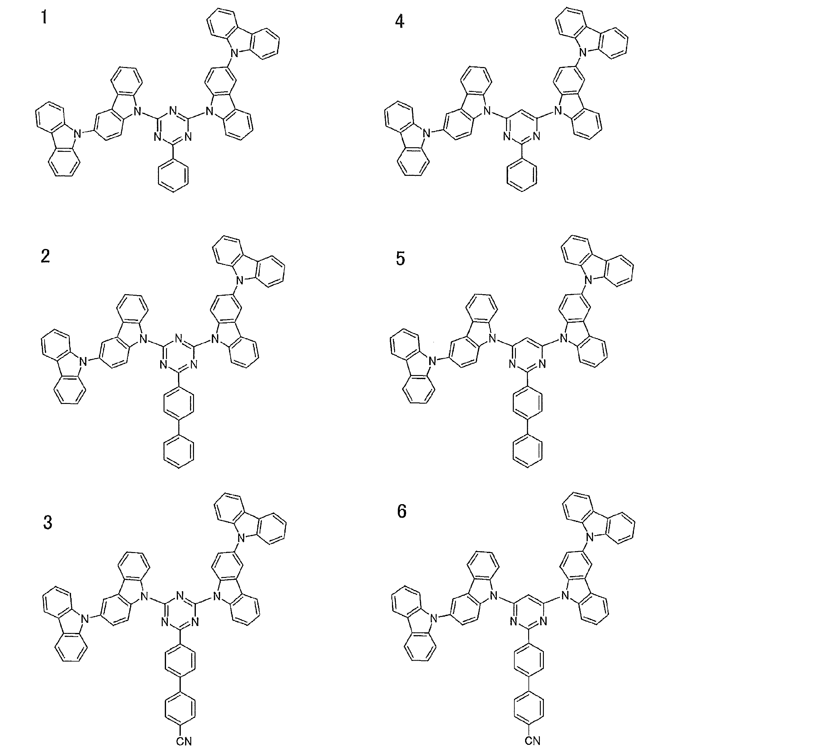
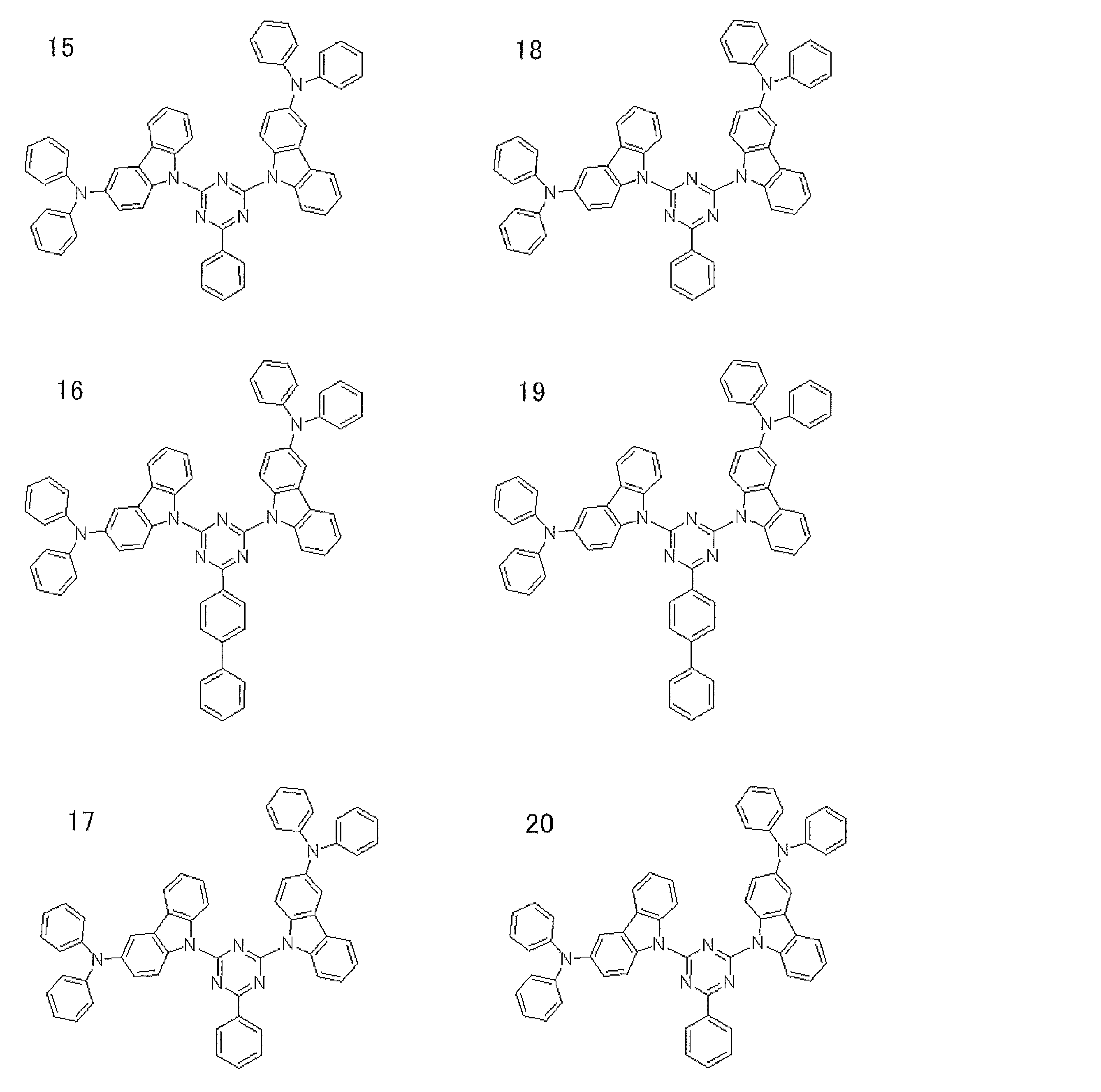
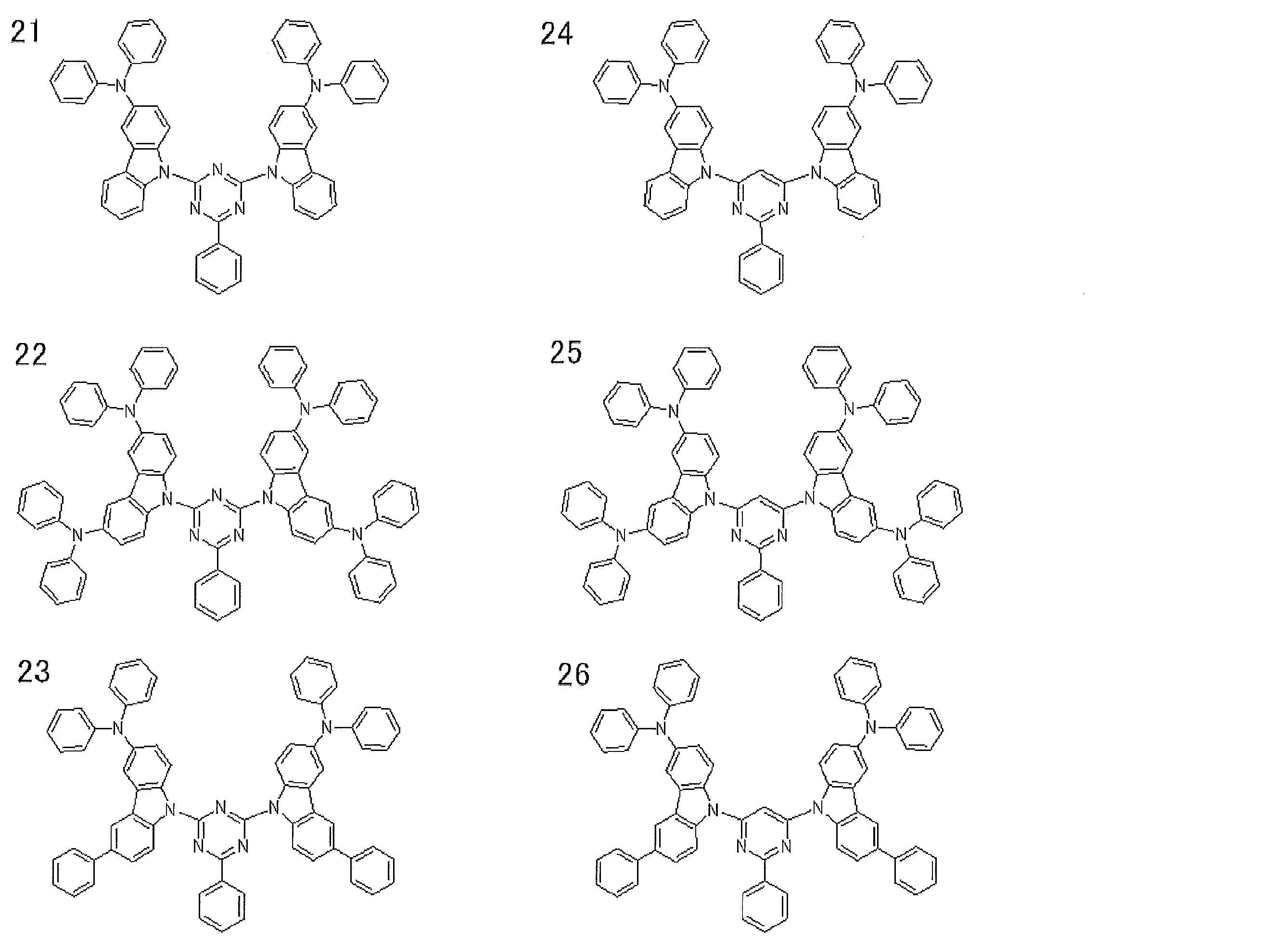
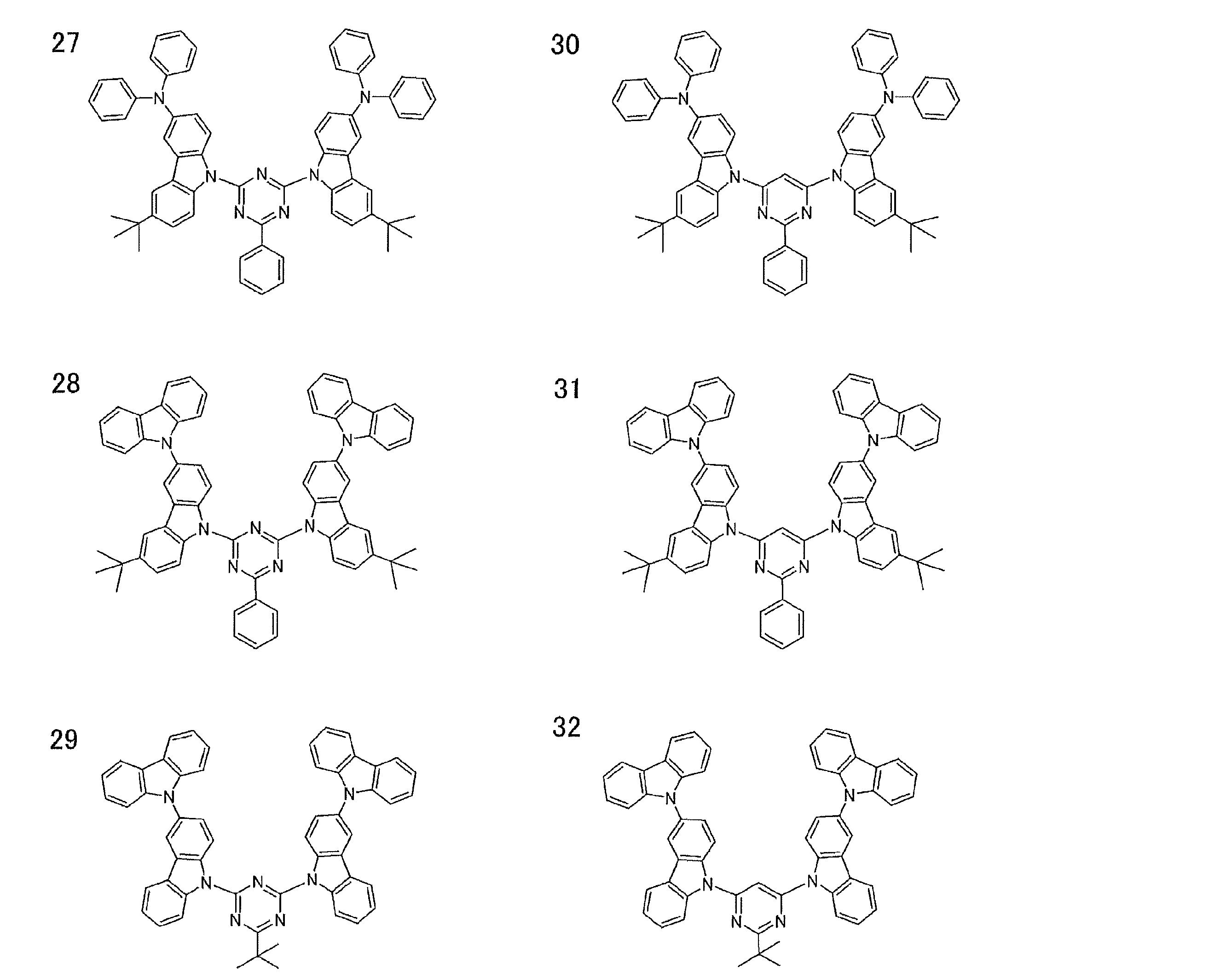
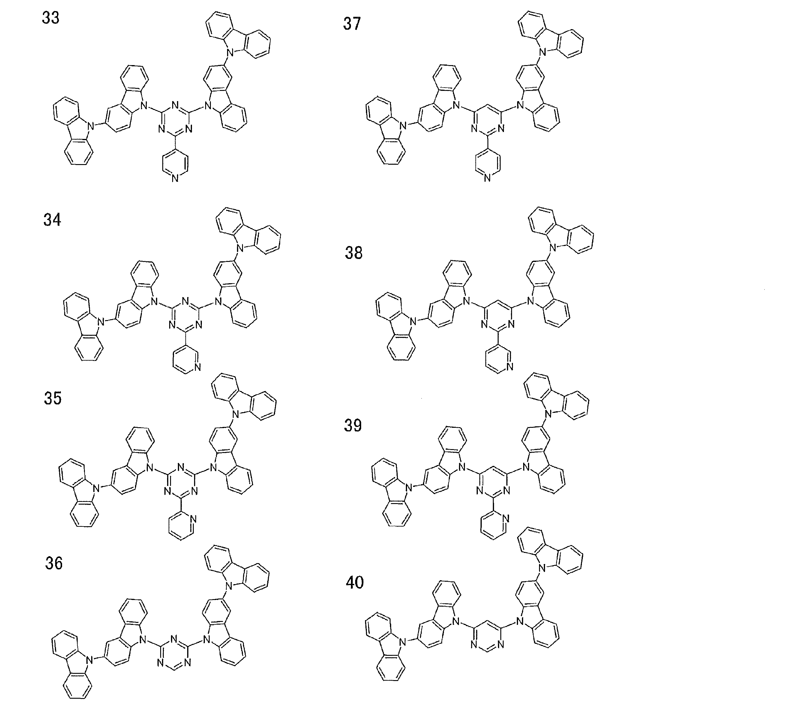
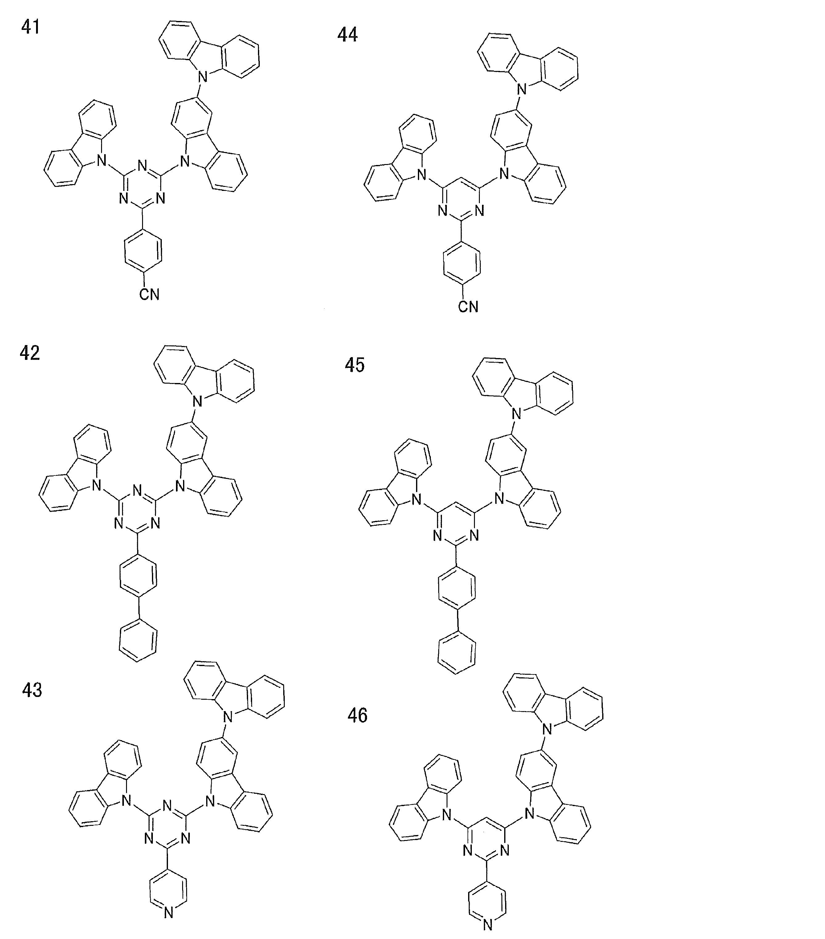
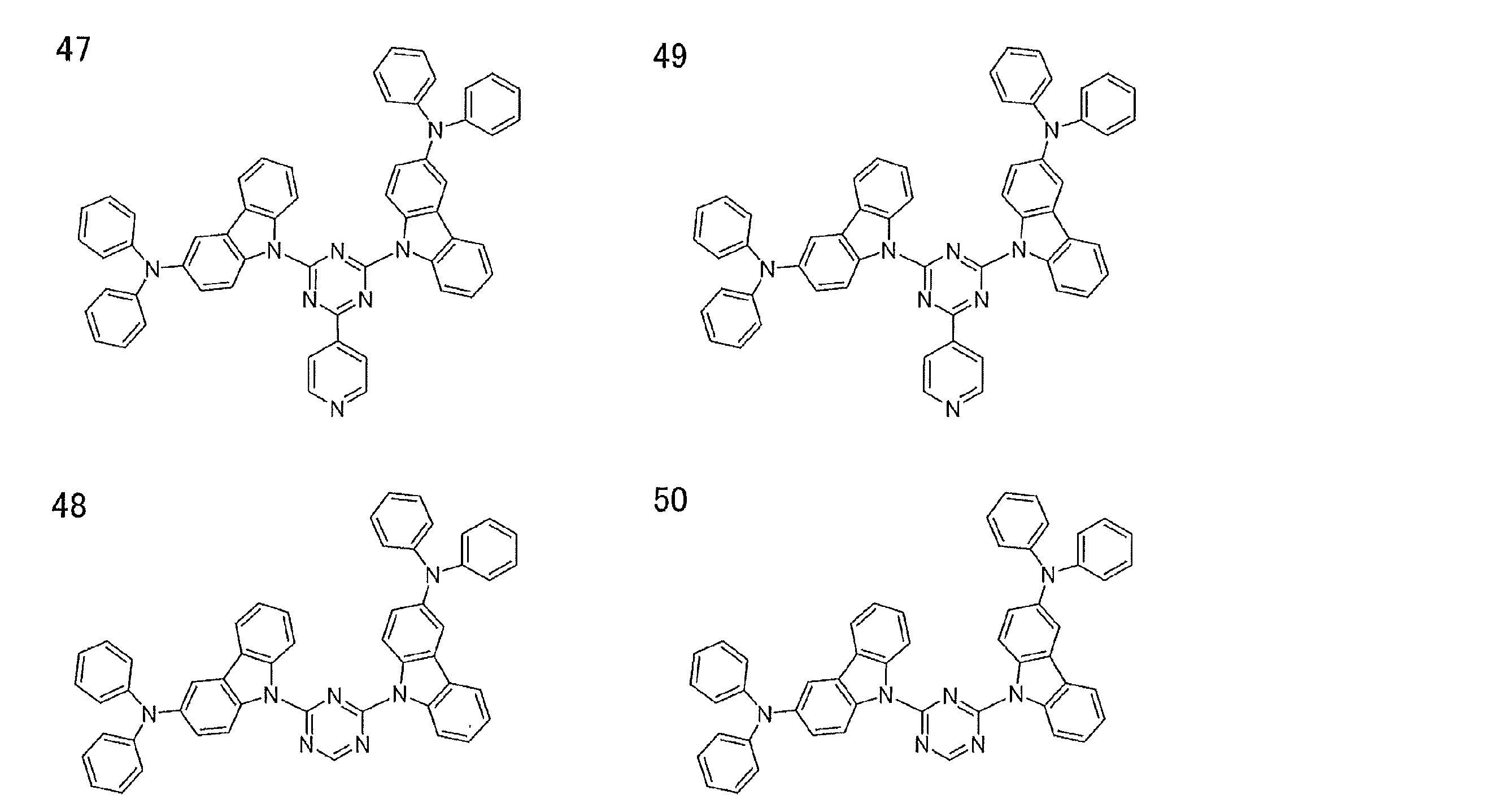
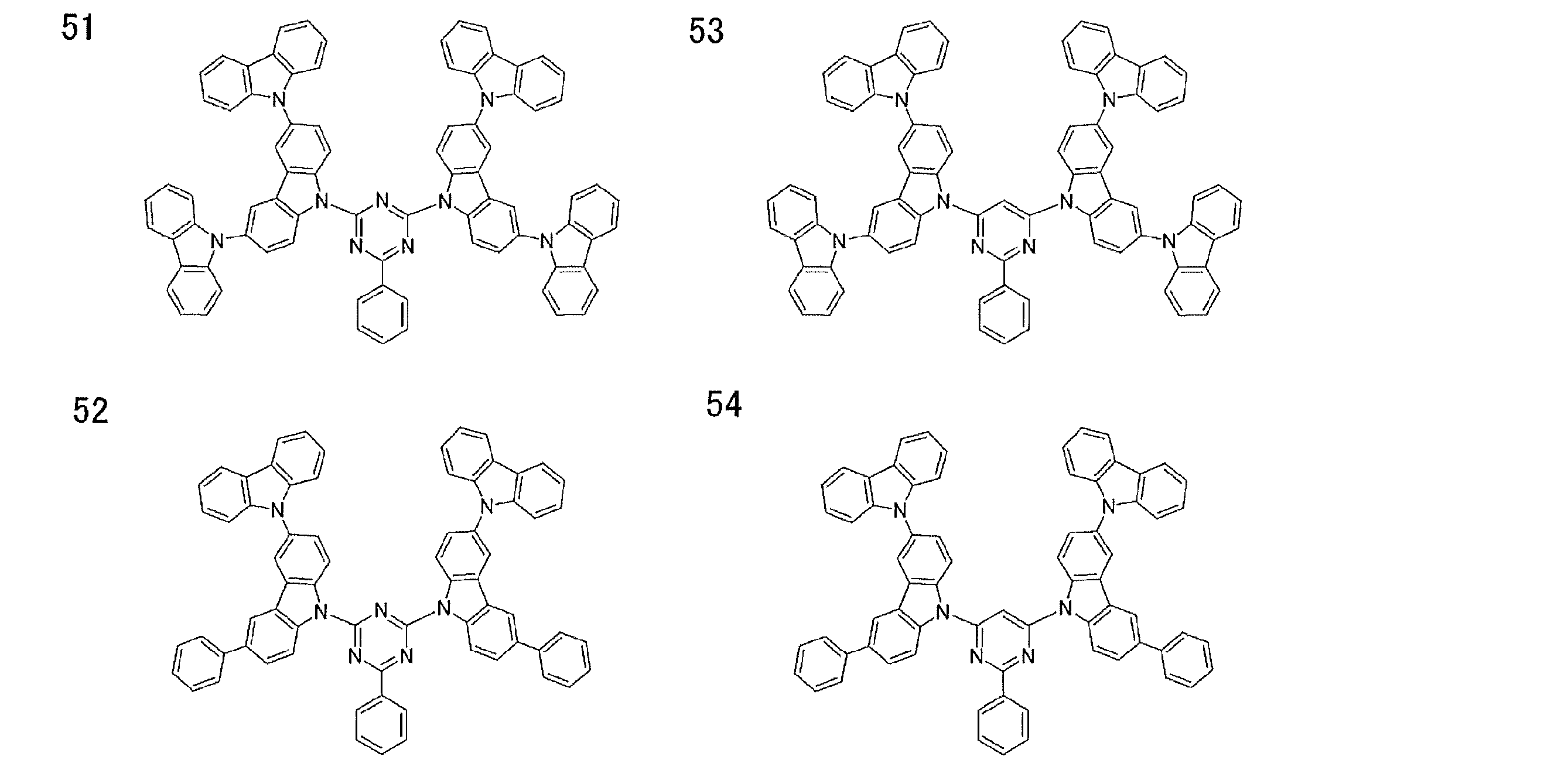
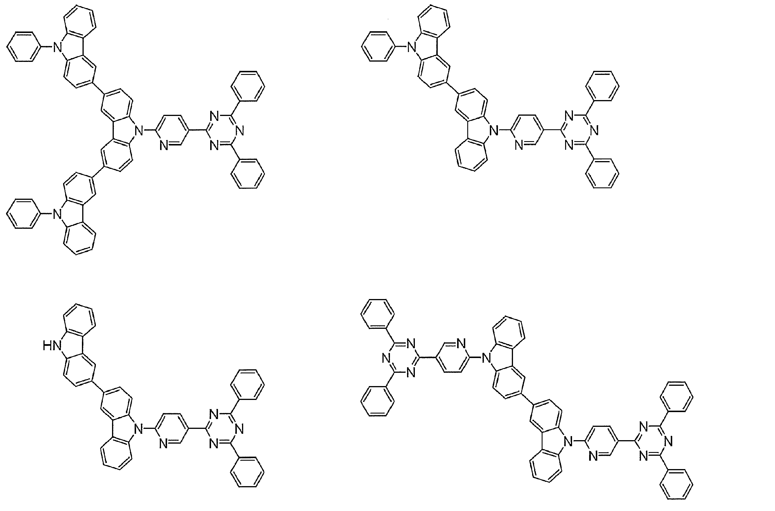
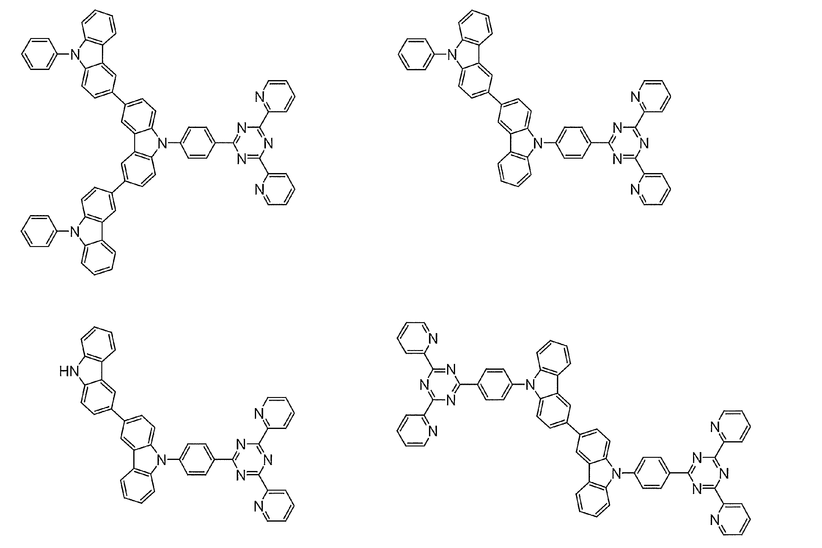
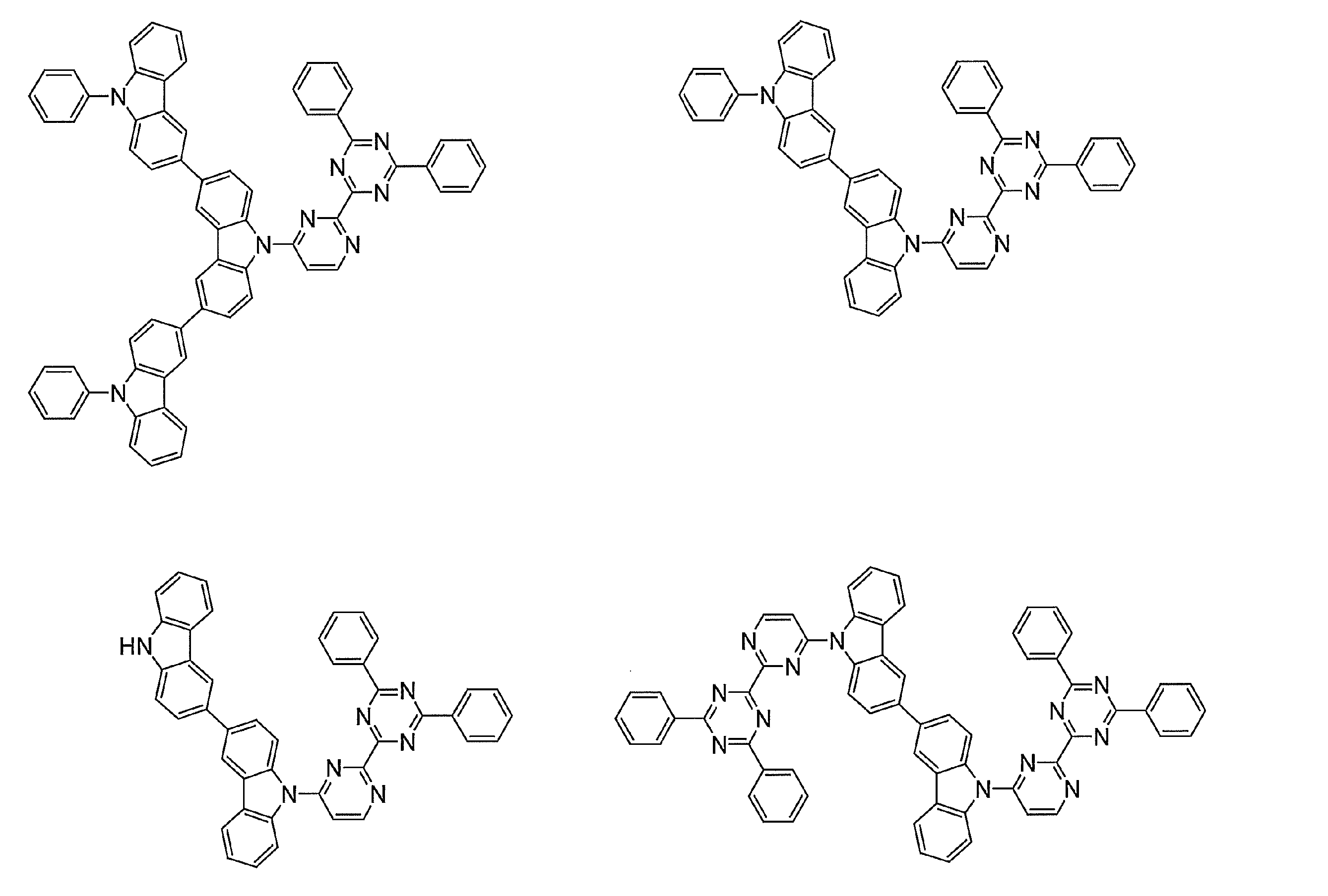
- Preferred examples of the luminescent material that can emit delayed fluorescence include compounds represented by the following general formula.
- the entire specification of the publication including the description of paragraphs 0008 to 0048 and 0095 to 0133 of WO2013 / 154064 is cited herein as a part of this specification.
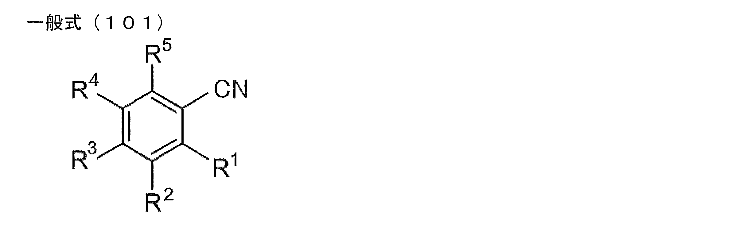
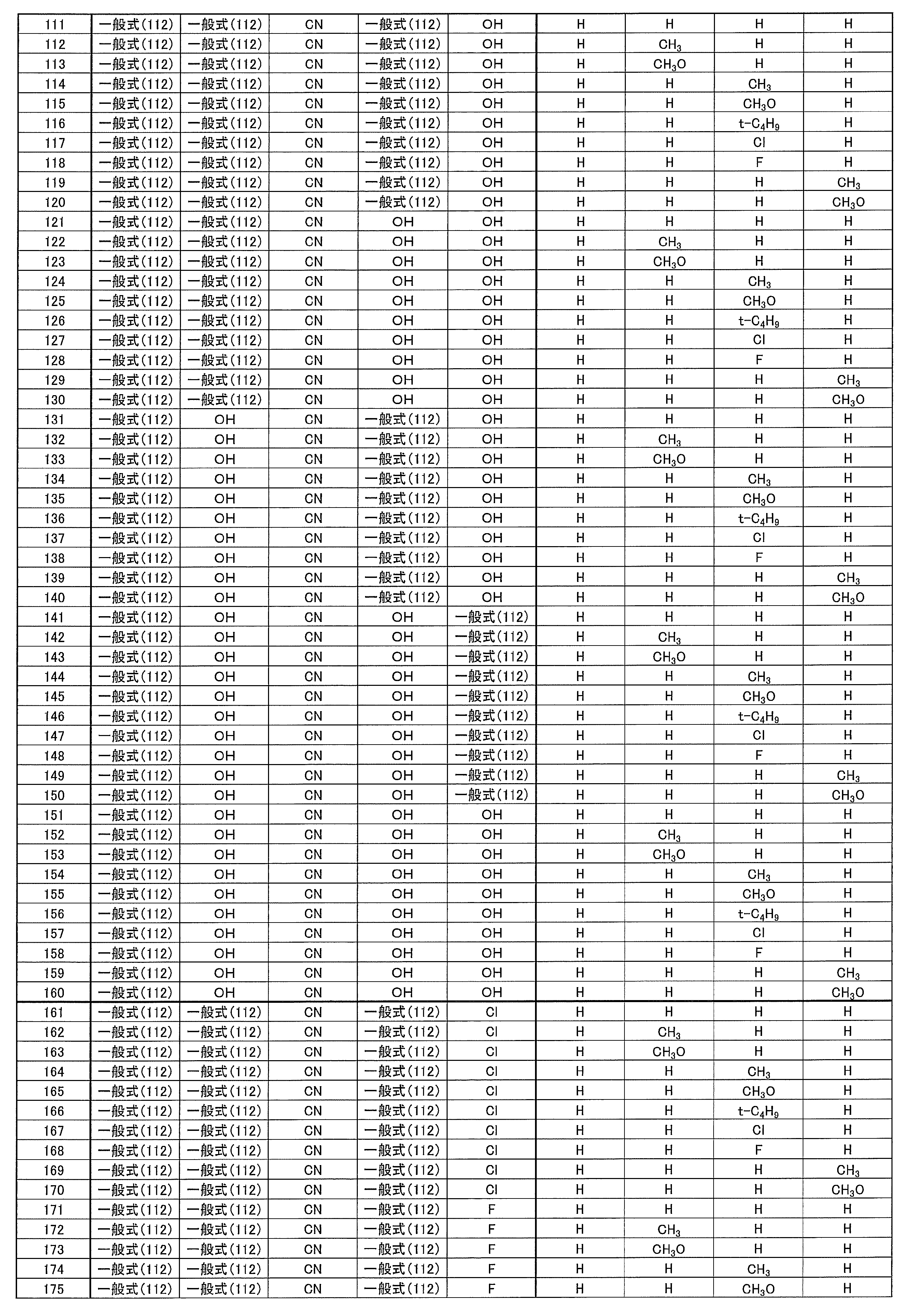
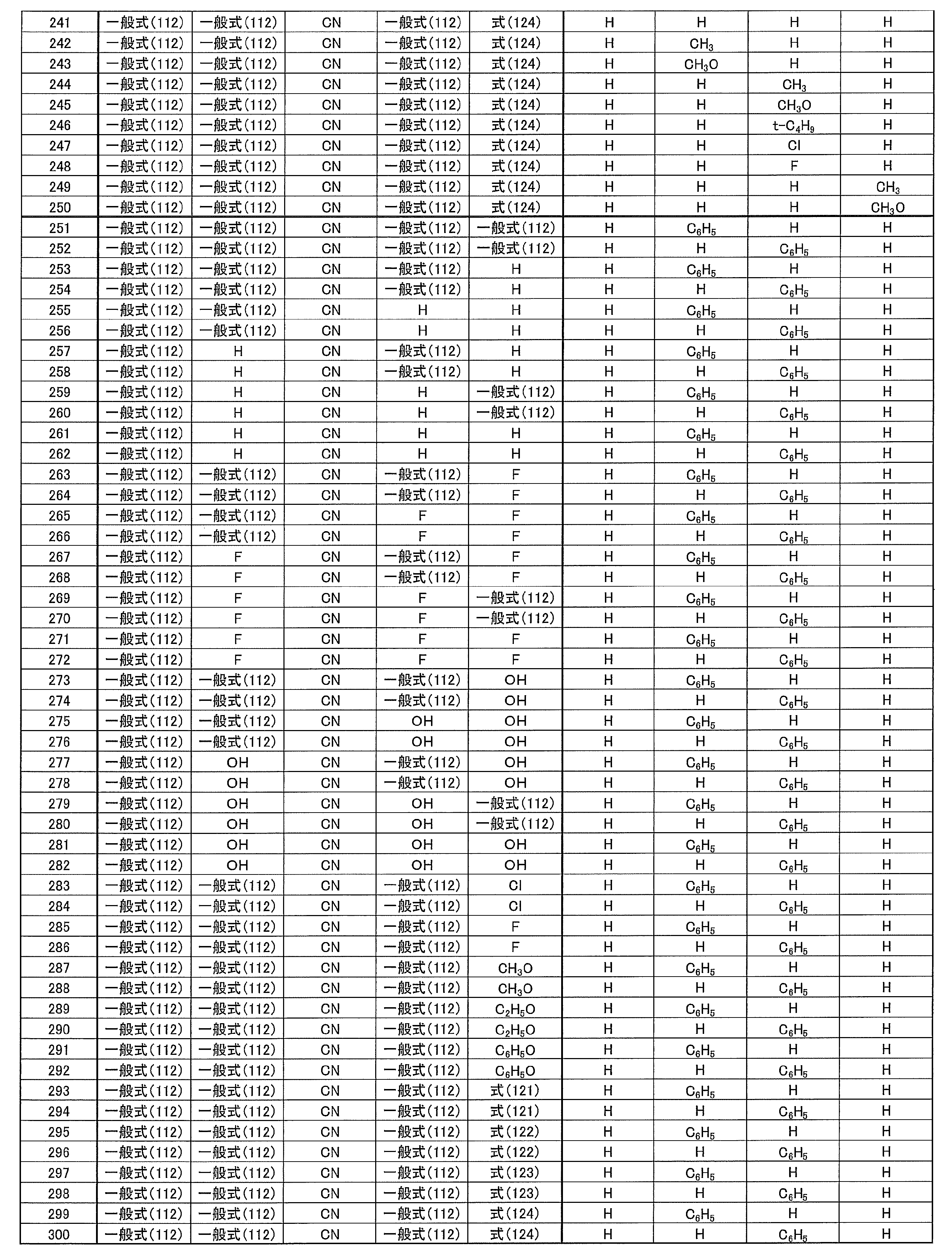
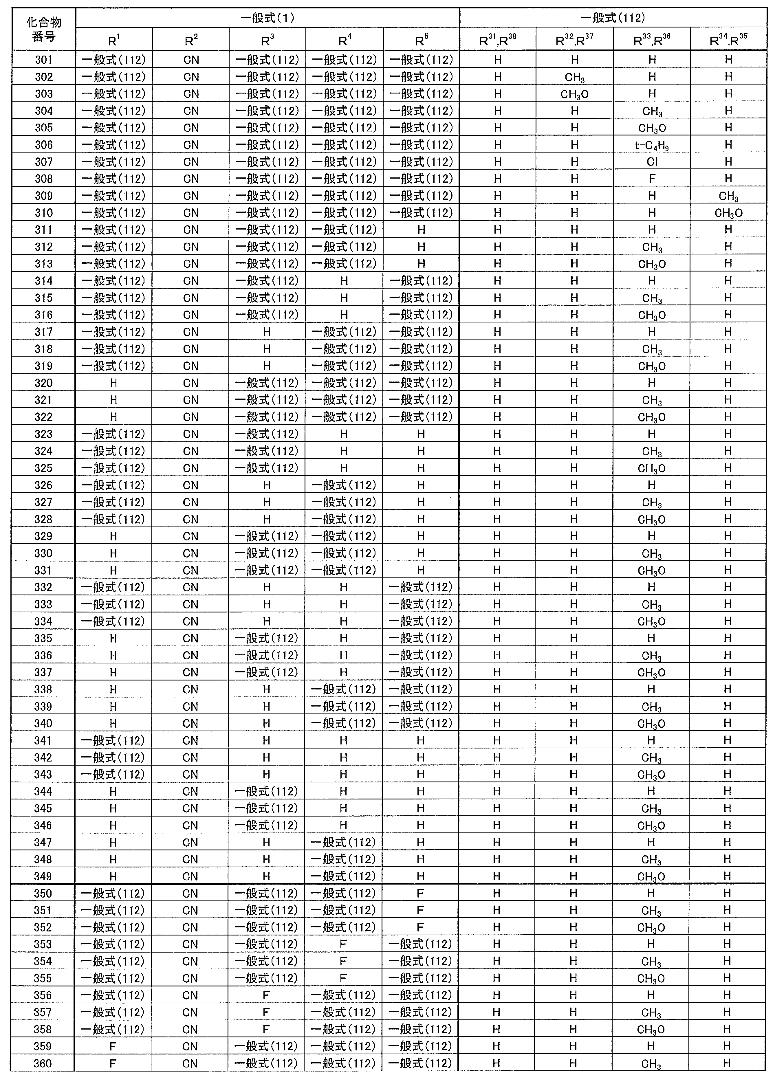
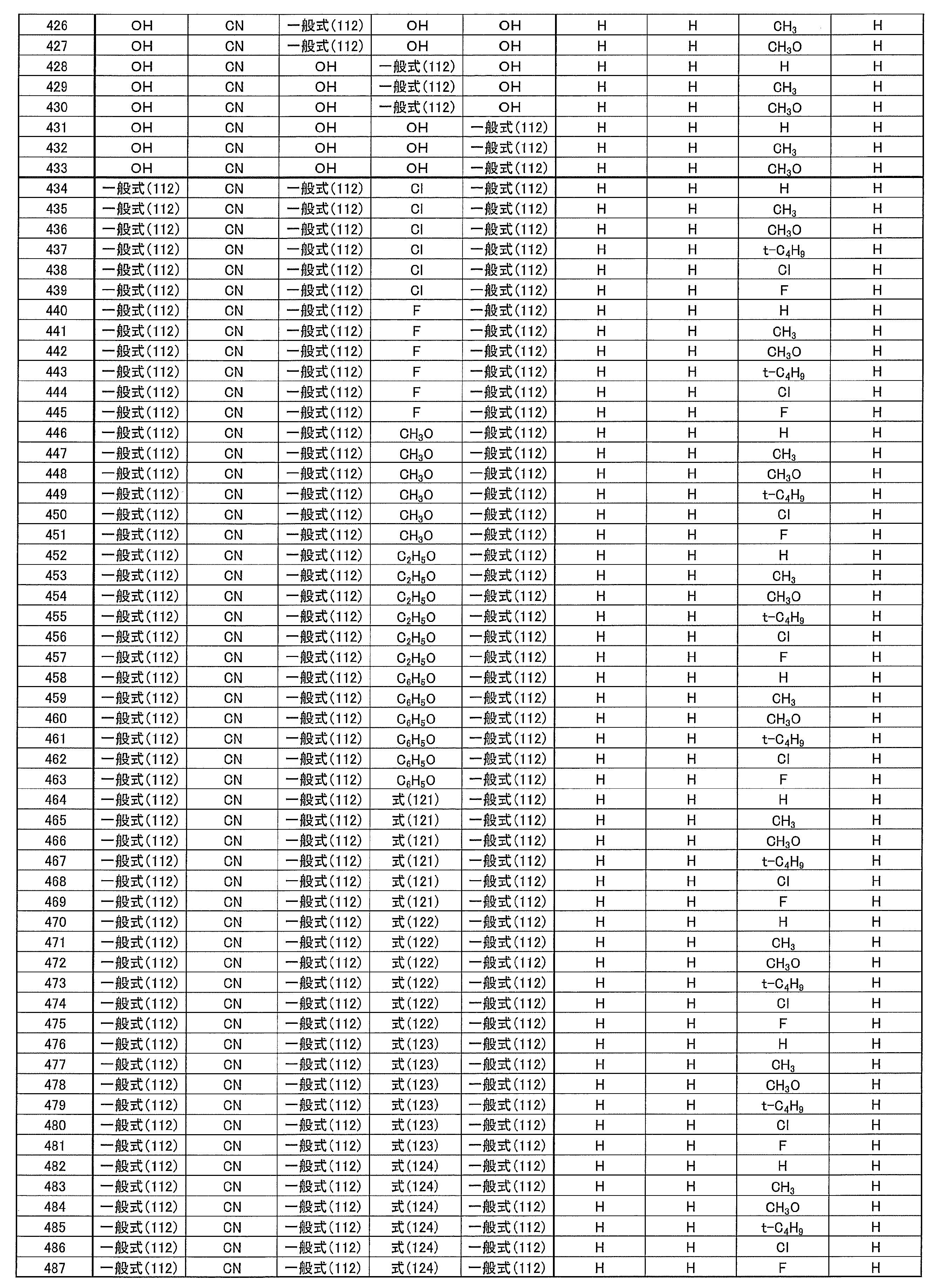
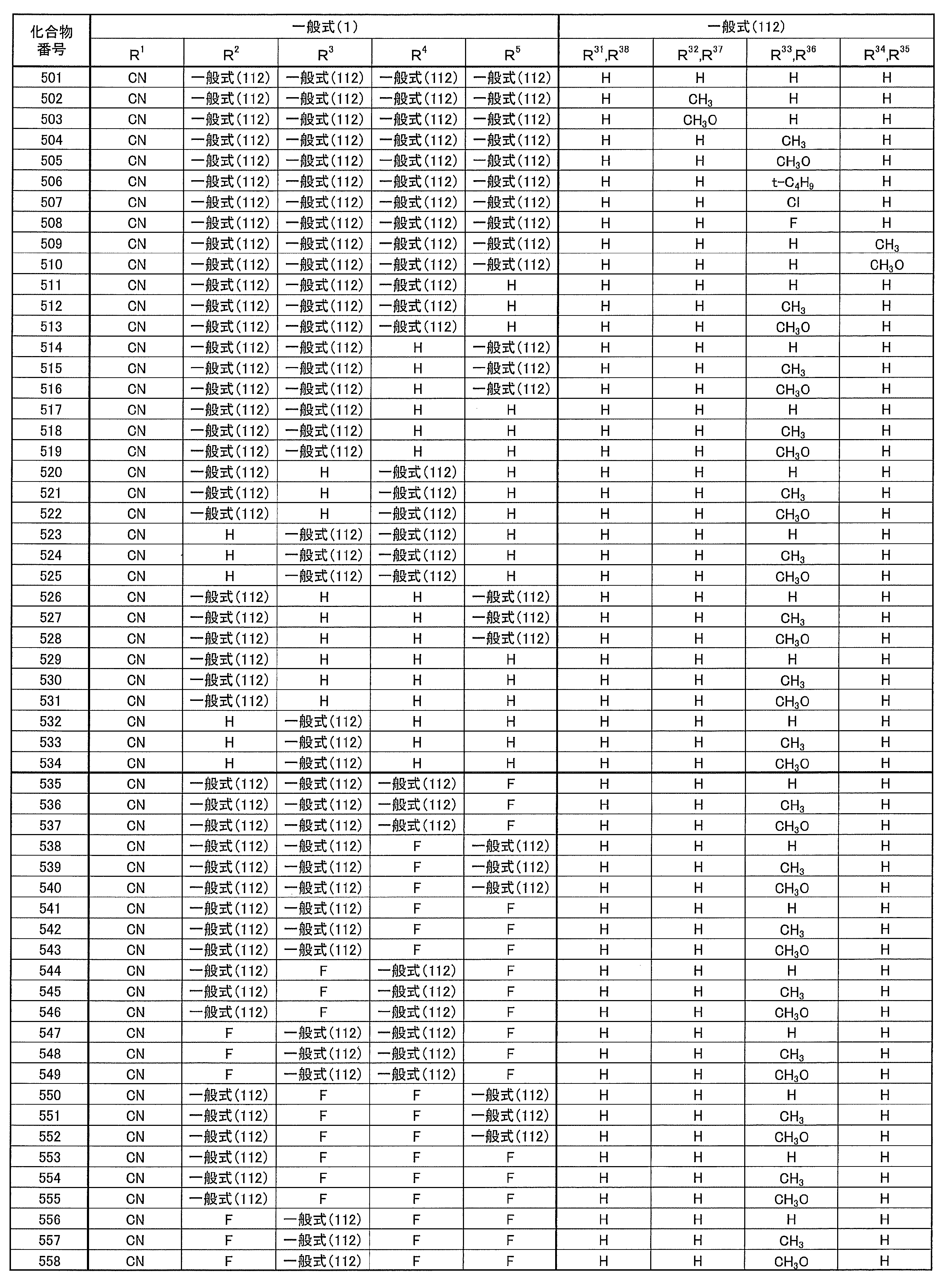
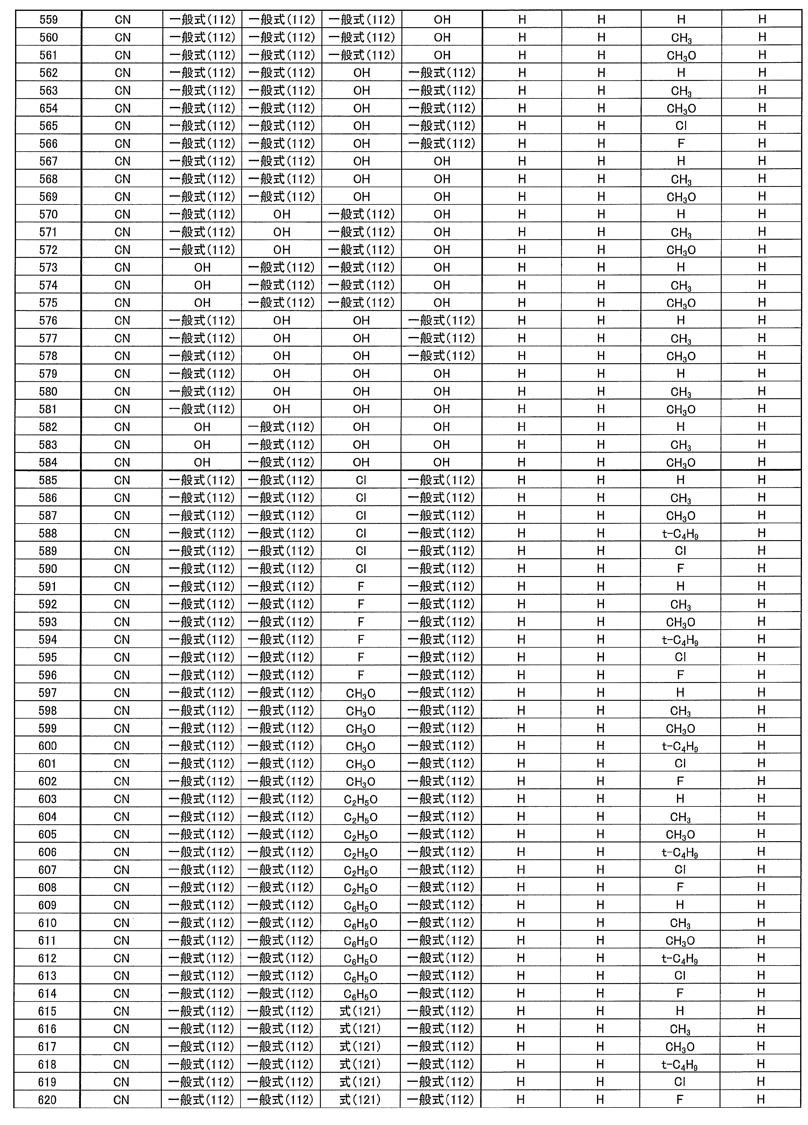
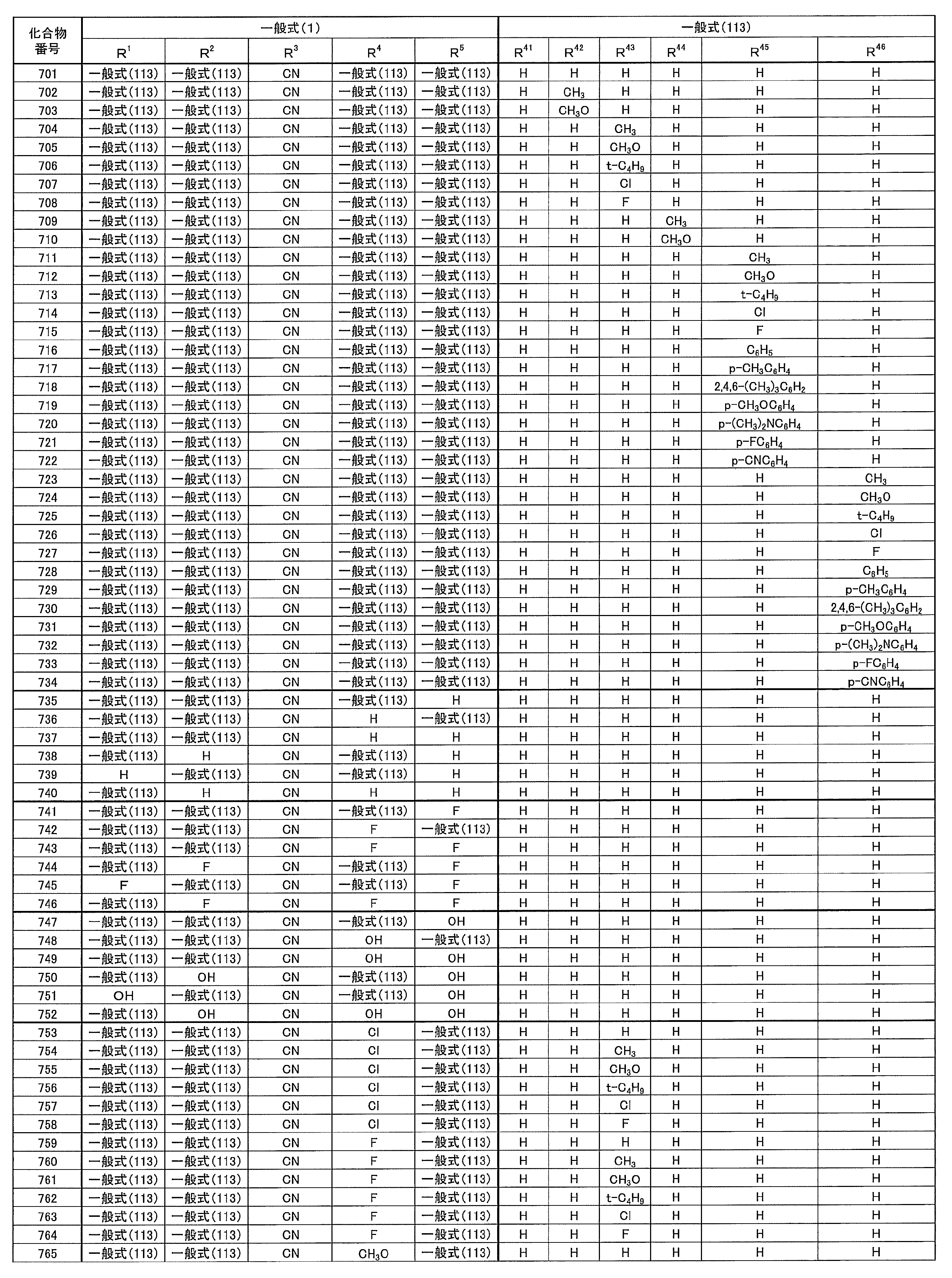
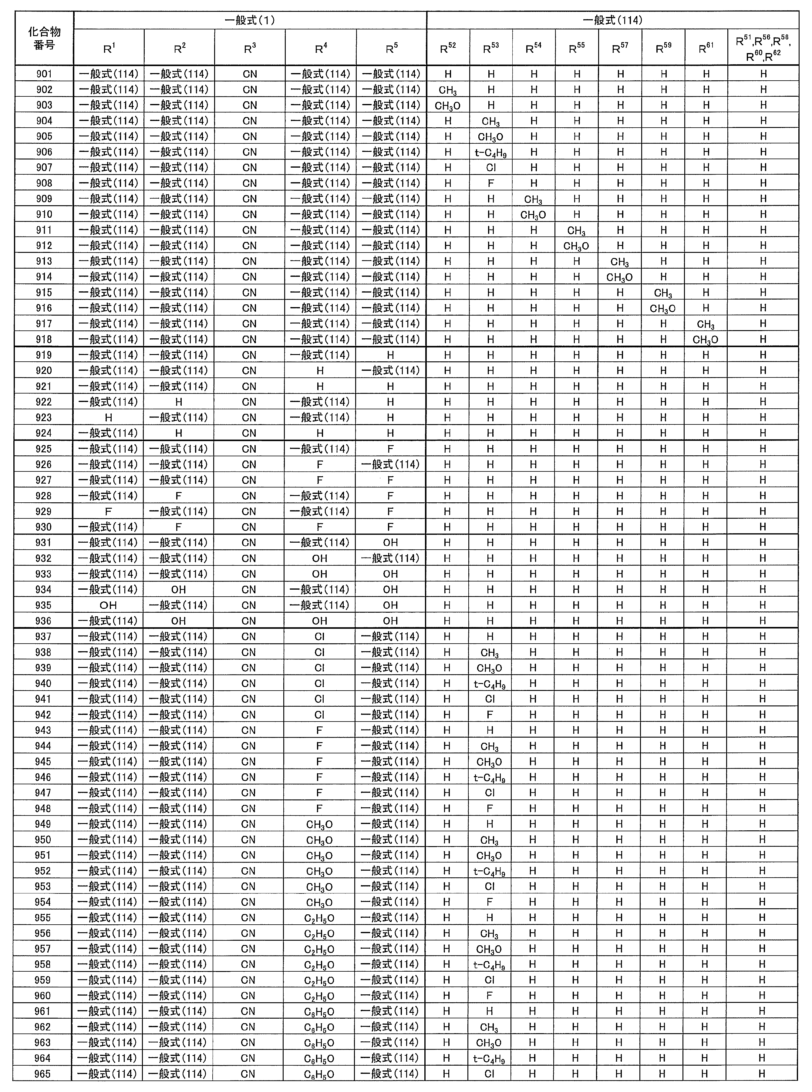
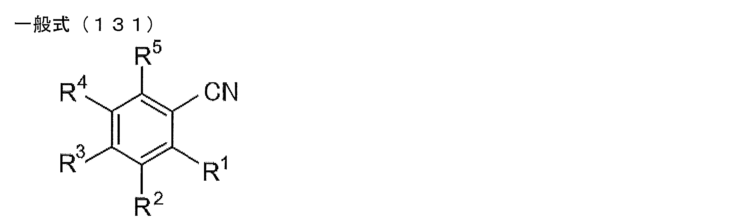
- at least one of R 1 ⁇ R 5 represents a cyano group
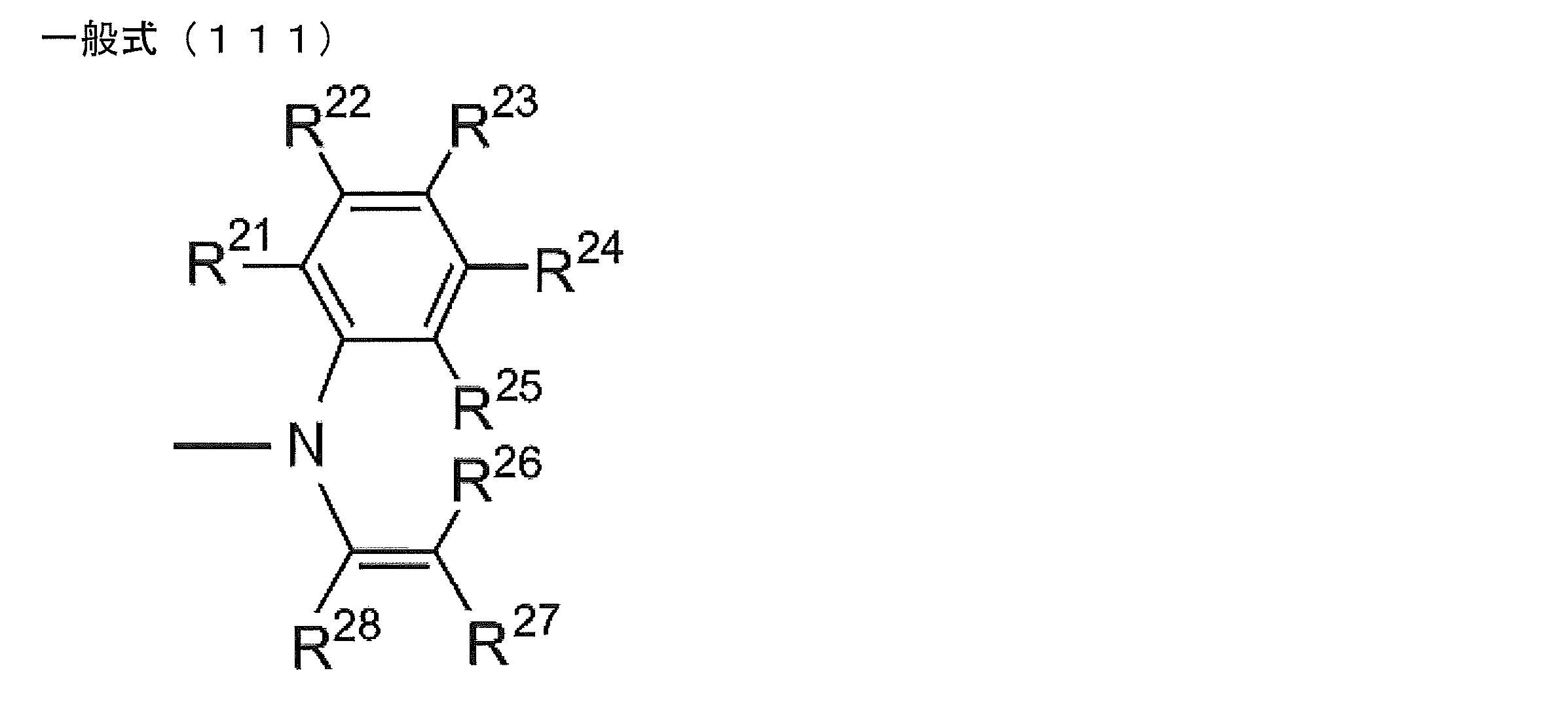
- at least one of R 1 ⁇ R 5 represents a group represented by the following general formula (111)
- the remaining R 1 to R 5 each represents a hydrogen atom or a substituent.
- R 21 to R 28 each independently represents a hydrogen atom or a substituent.
- ⁇ A> R 25 and R 26 together form a single bond.
- ⁇ B> R 27 and R 28 together represent an atomic group necessary for forming a substituted or unsubstituted benzene ring.
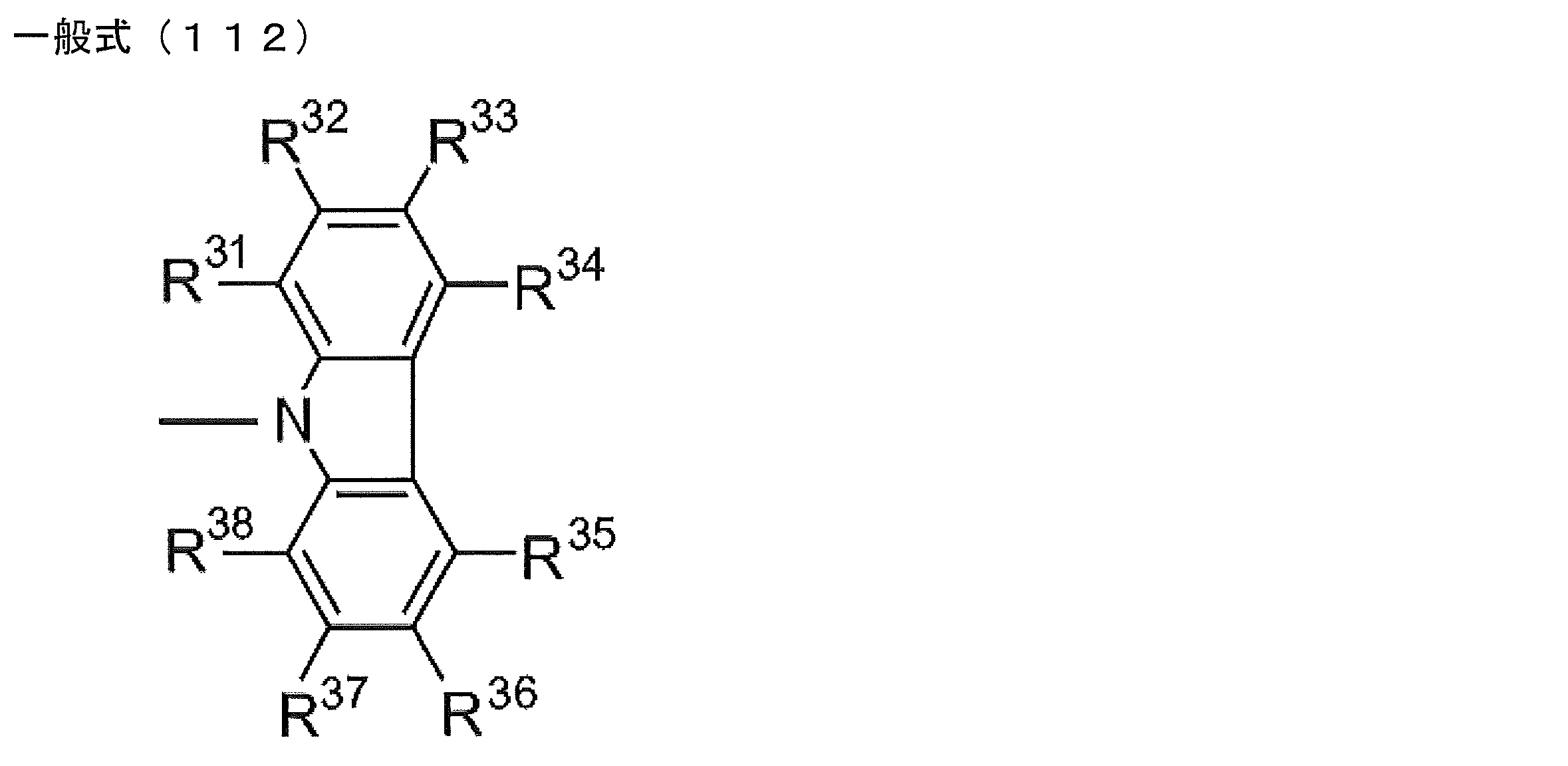
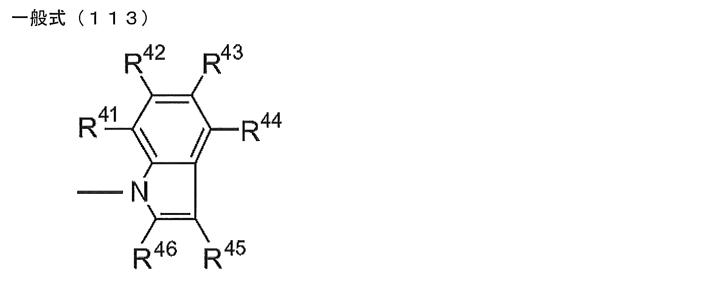
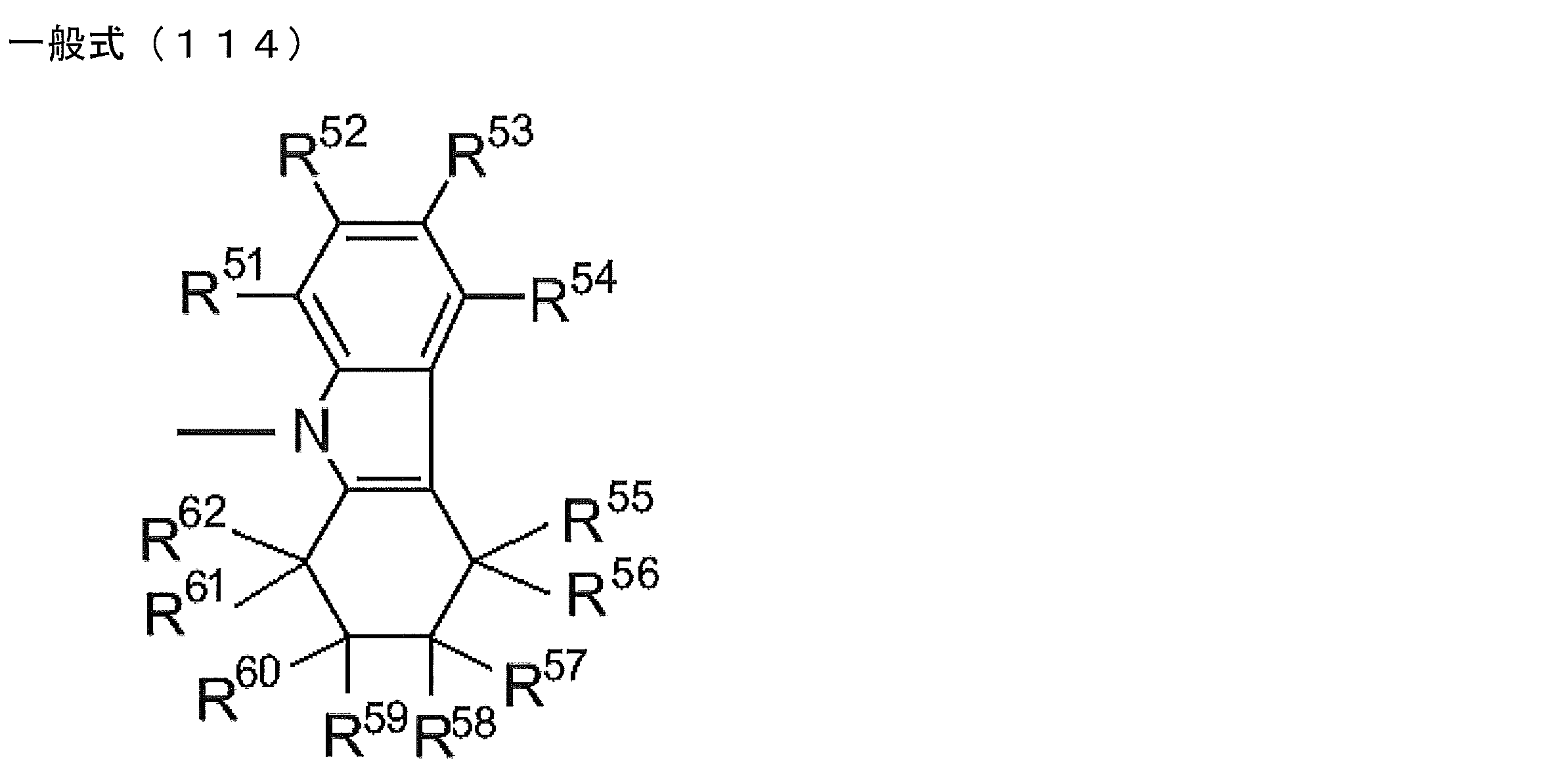
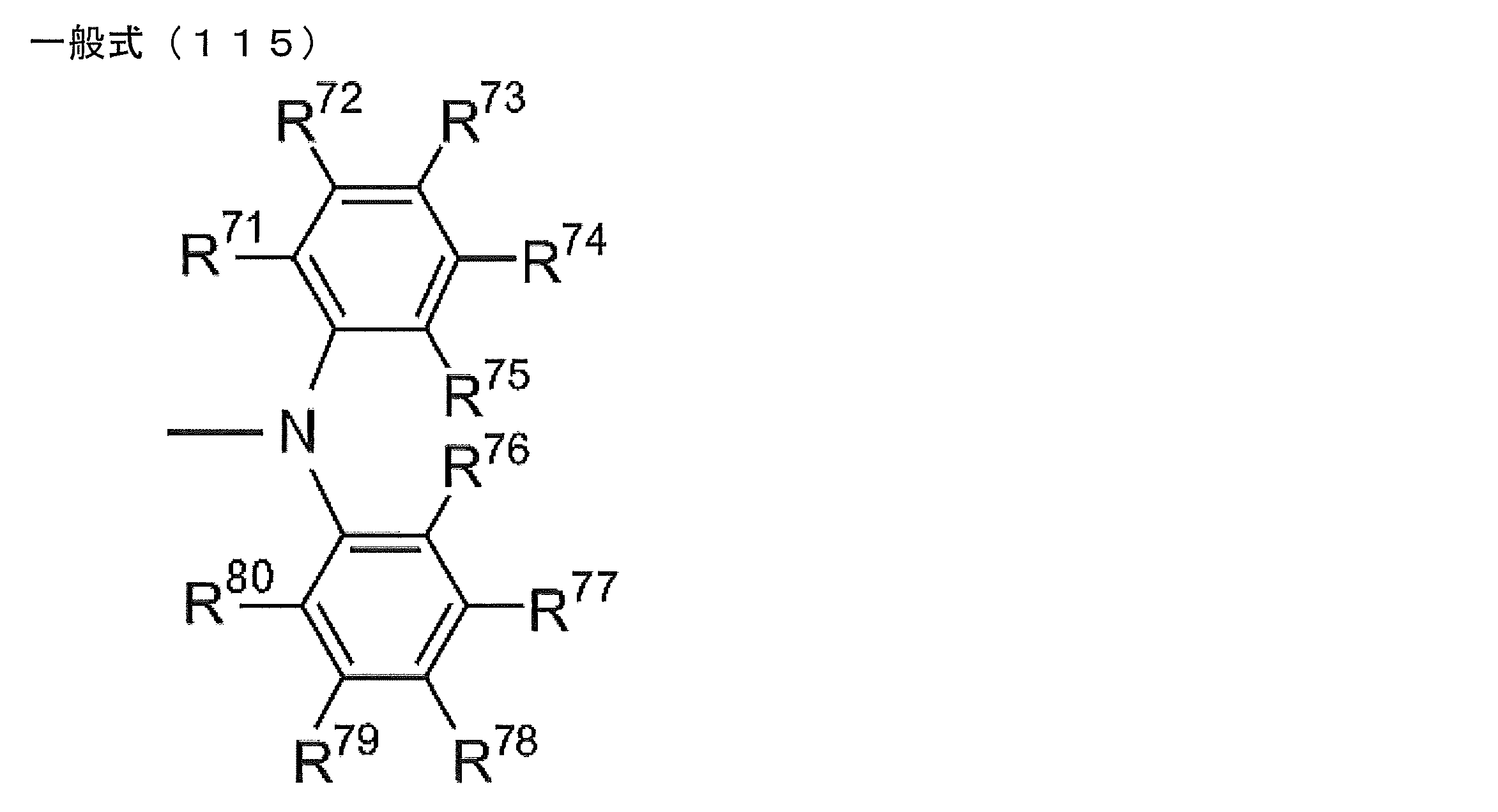
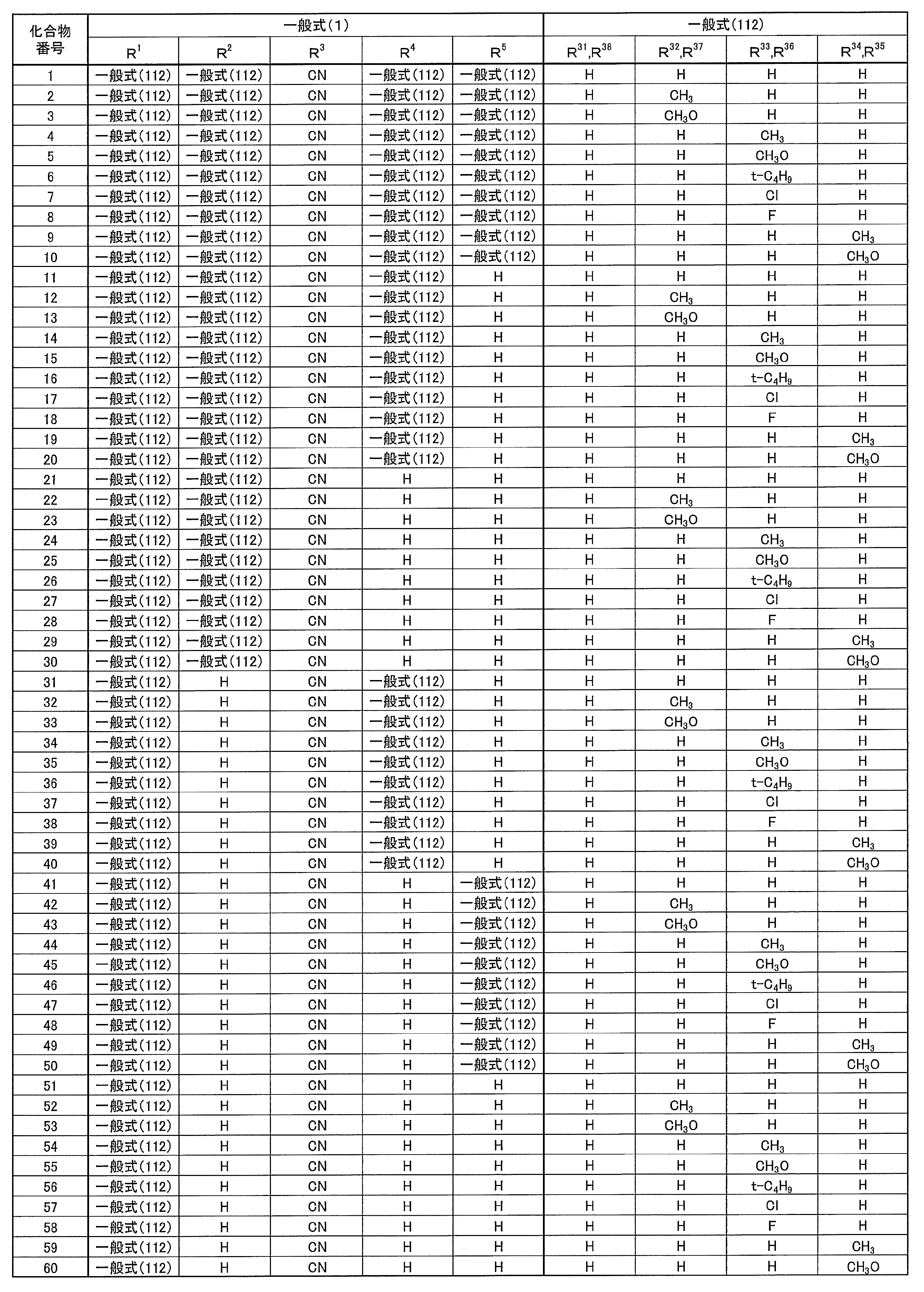
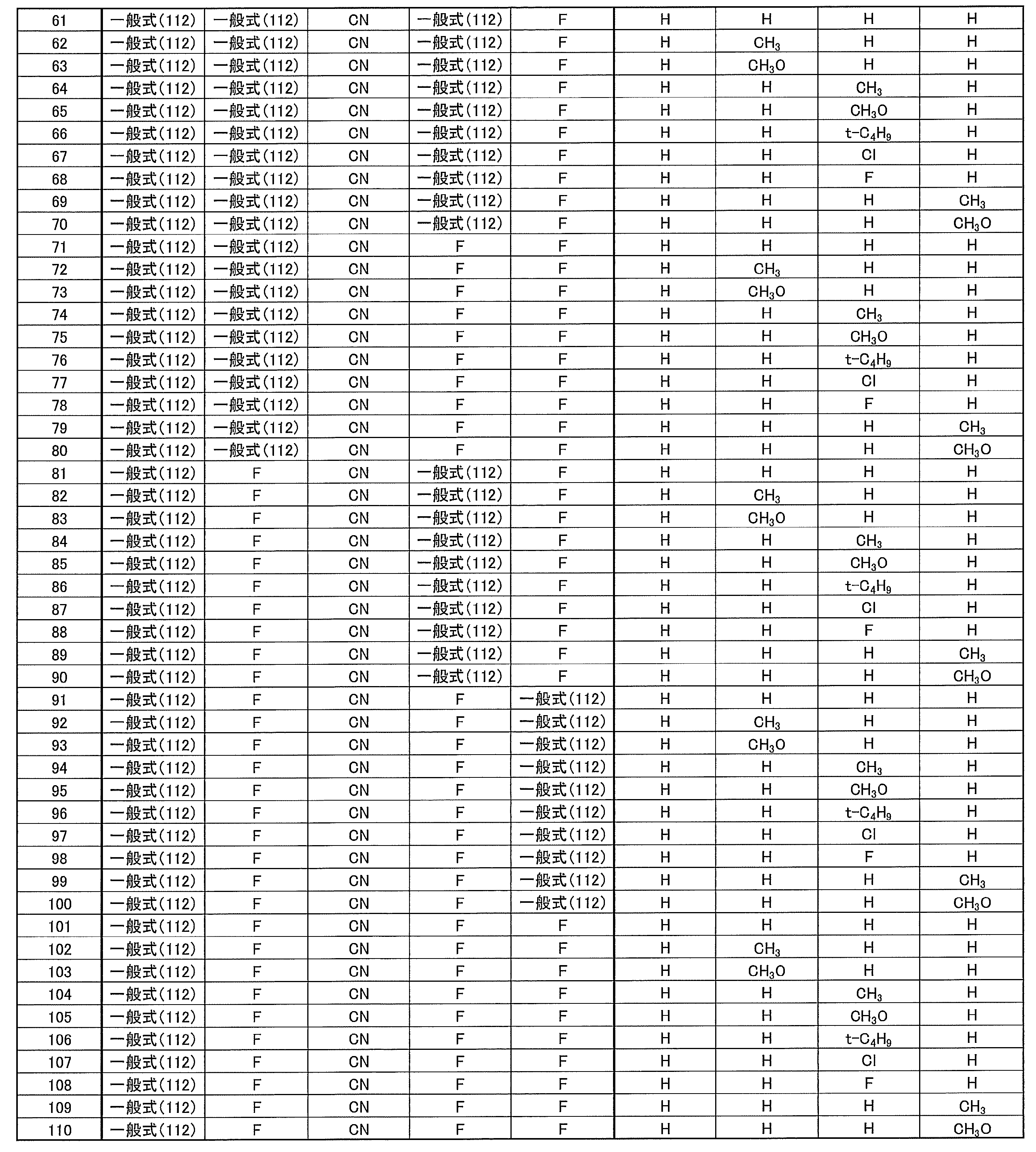
- R 1 to R 5 is preferably a group represented by any one of the following general formulas (112) to (115).
- R 31 to R 38 each independently represents a hydrogen atom or a substituent.
- R 41 to R 46 each independently represents a hydrogen atom or a substituent.
- R 51 to R 62 each independently represents a hydrogen atom or a substituent.
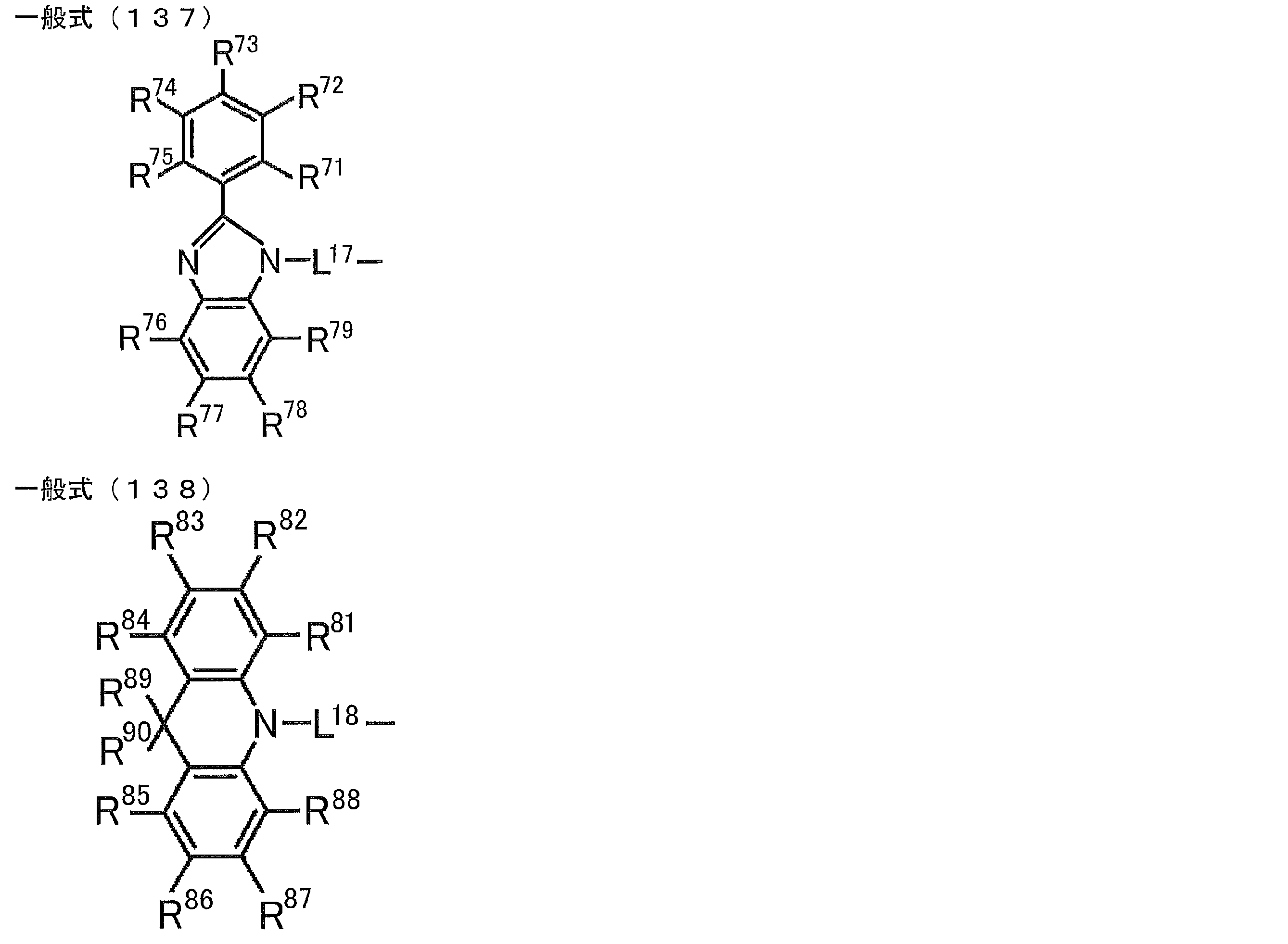
- R 71 to R 80 each independently represents a hydrogen atom or a substituent.
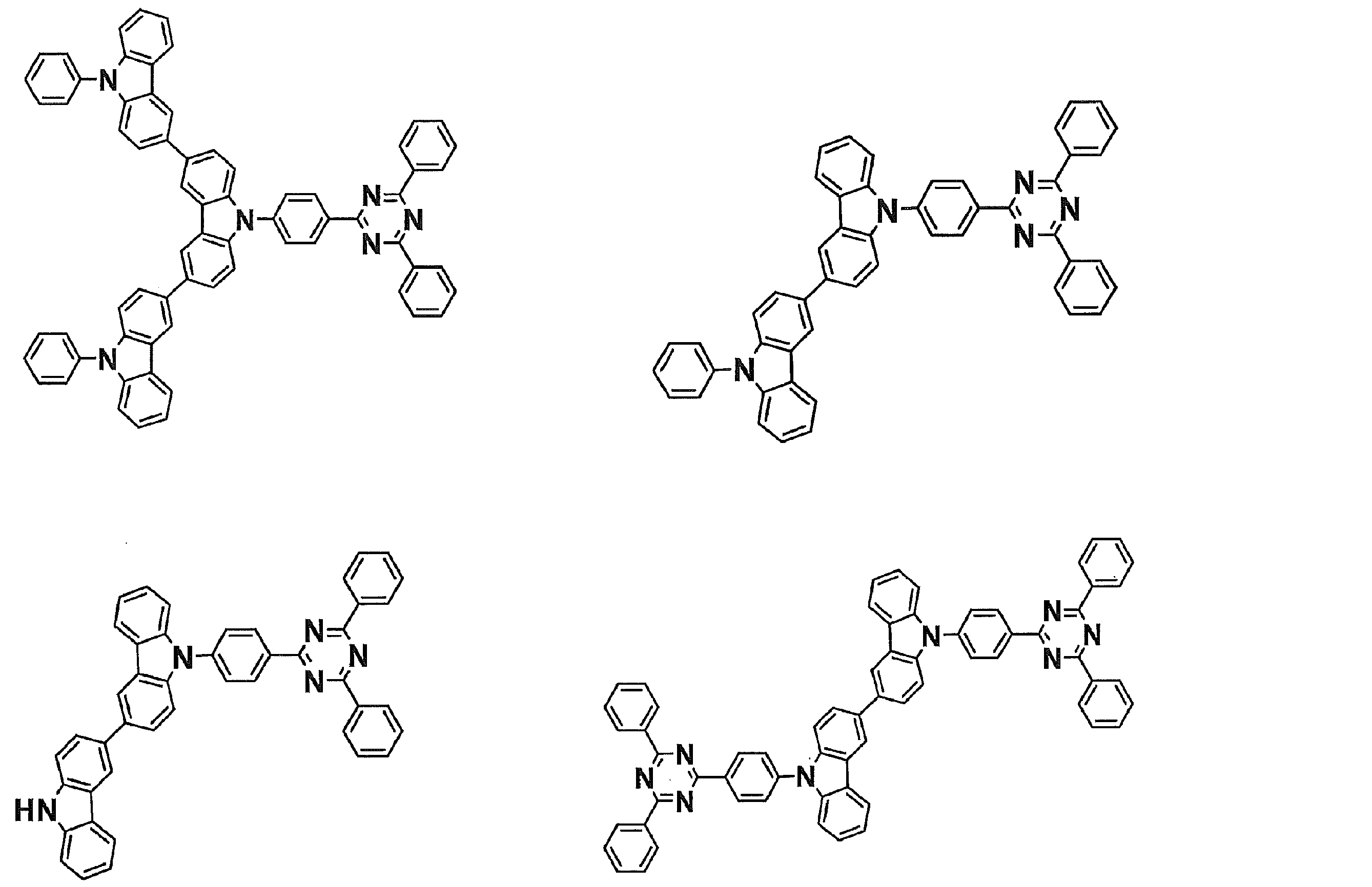
- Examples of preferable luminescent materials that can emit delayed fluorescence include the following compounds.
- 0 to 1 of R 1 to R 5 are cyano groups
- 1 to 5 of R 1 to R 5 are groups represented by the following General Formula (132)
- the rest R 1 to R 5 are a hydrogen atom or a substituent other than those described above.
- R 11 to R 20 each independently represents a hydrogen atom or a substituent.
- R 11 and R 12 , R 12 and R 13 , R 13 and R 14 , R 14 and R 15 , R 15 and R 16 , R 16 and R 17 , R 17 and R 18 , R 18 and R 19 , R 19 And R 20 may be bonded to each other to form a cyclic structure.
- L 12 represents a substituted or unsubstituted arylene group or a substituted or unsubstituted heteroarylene group.
- R 21 to R 24 , R 27 to R 38 , R 41 to R 48 , R 51 to R 58 , R 61 to R 65 , R 71 to R 79 , R 81 R 90 each independently represents a hydrogen atom or a substituent.
- L 13 to L 18 each independently represents a substituted or unsubstituted arylene group or a substituted or unsubstituted heteroarylene group.
- [3] The compound according to [1] or [2], wherein R 3 in the general formula (131) is a cyano group.
- [4] The compound according to any one of [1] to [3], wherein R 1 and R 4 in the general formula (131) are a group represented by the general formula (132).
- [5] The compound according to any one of [1] to [4], wherein L 12 in the general formula (132) is a phenylene group.
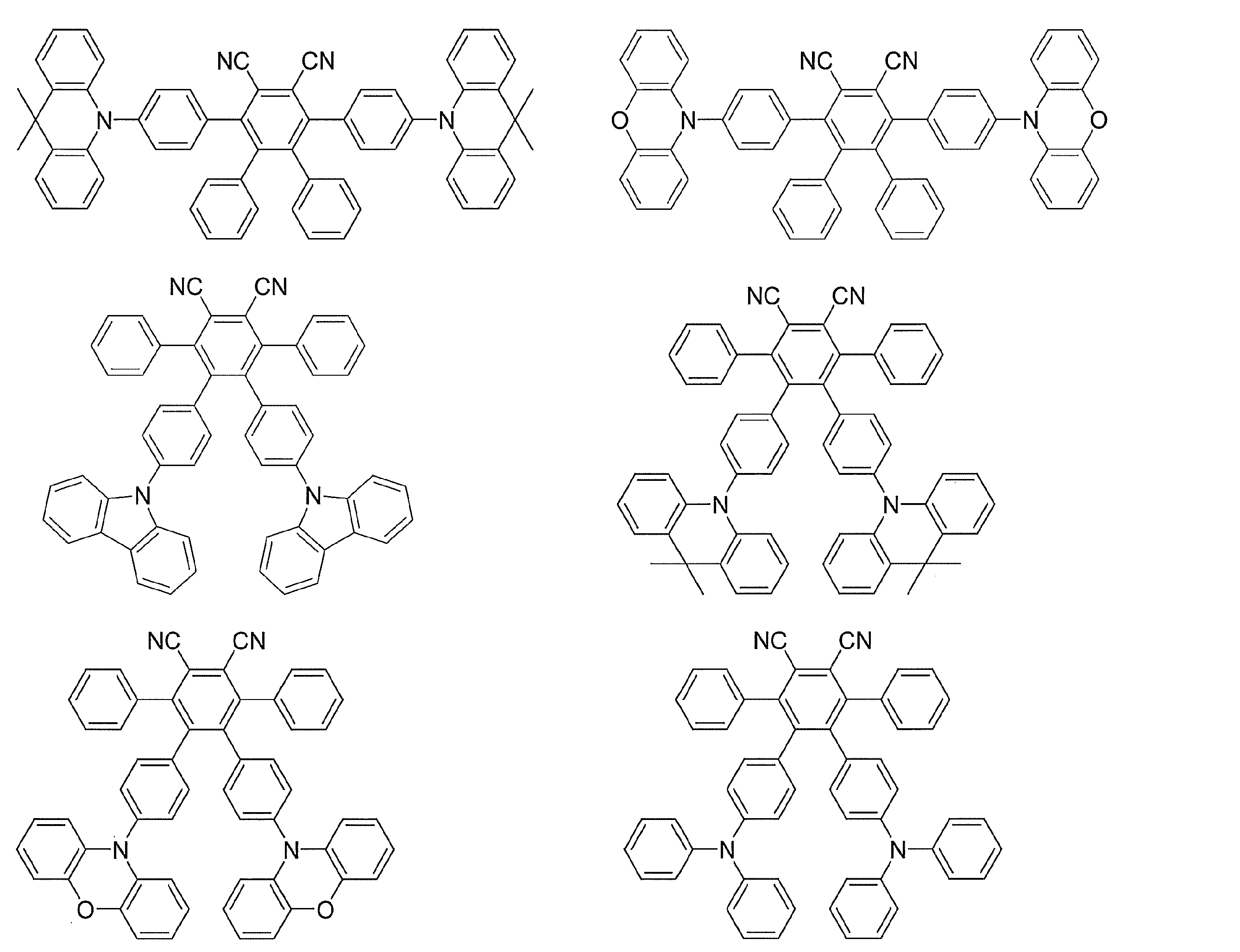
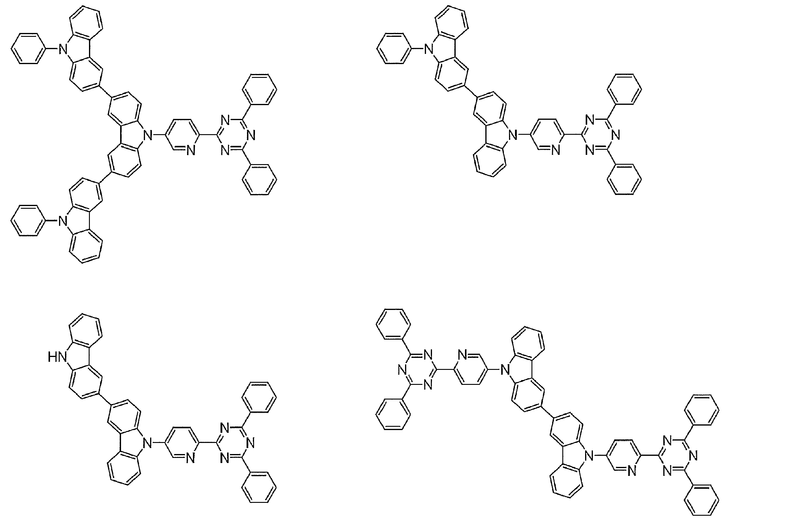
- Preferred examples of the luminescent material that can emit delayed fluorescence include compounds represented by the following general formula.
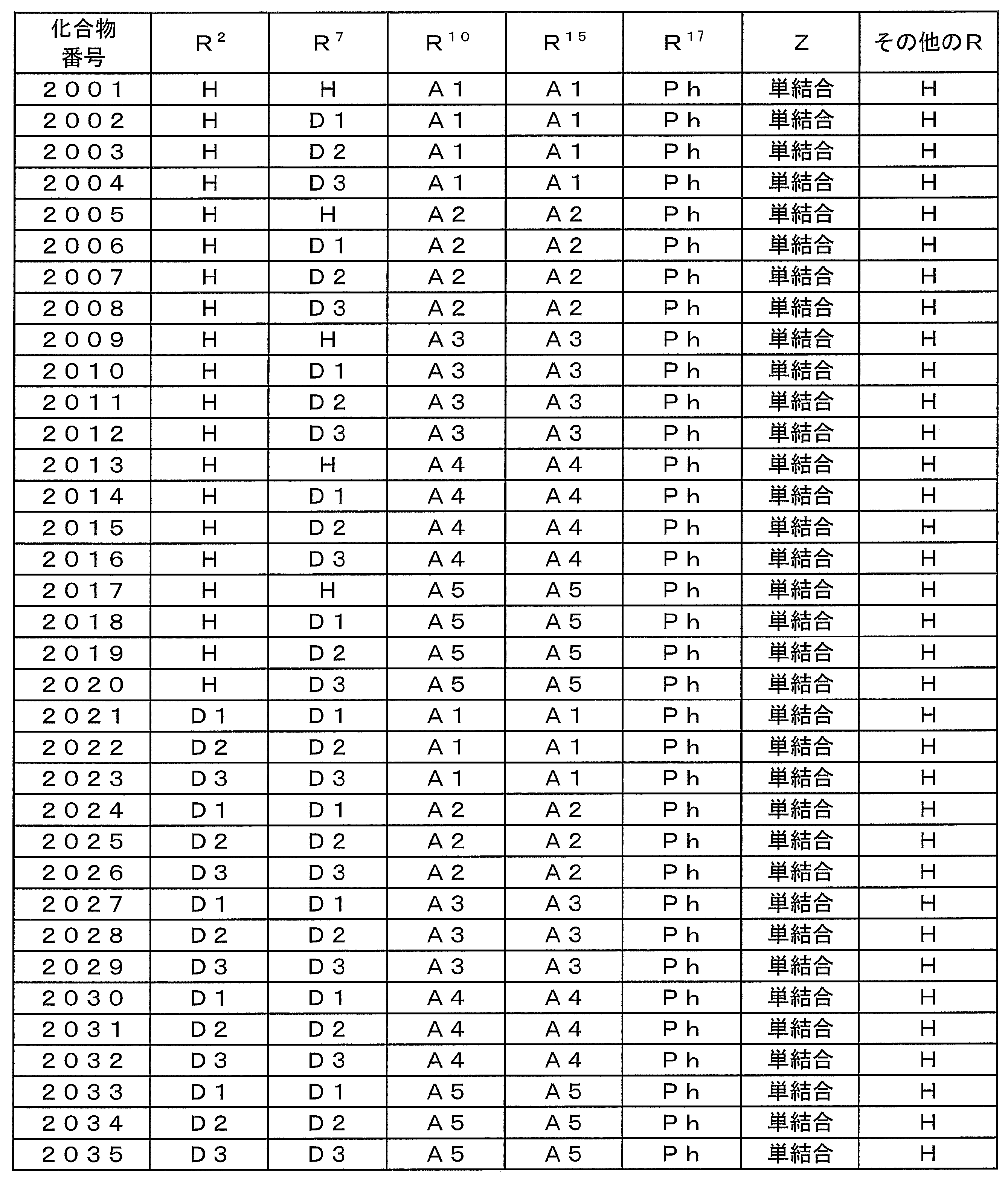
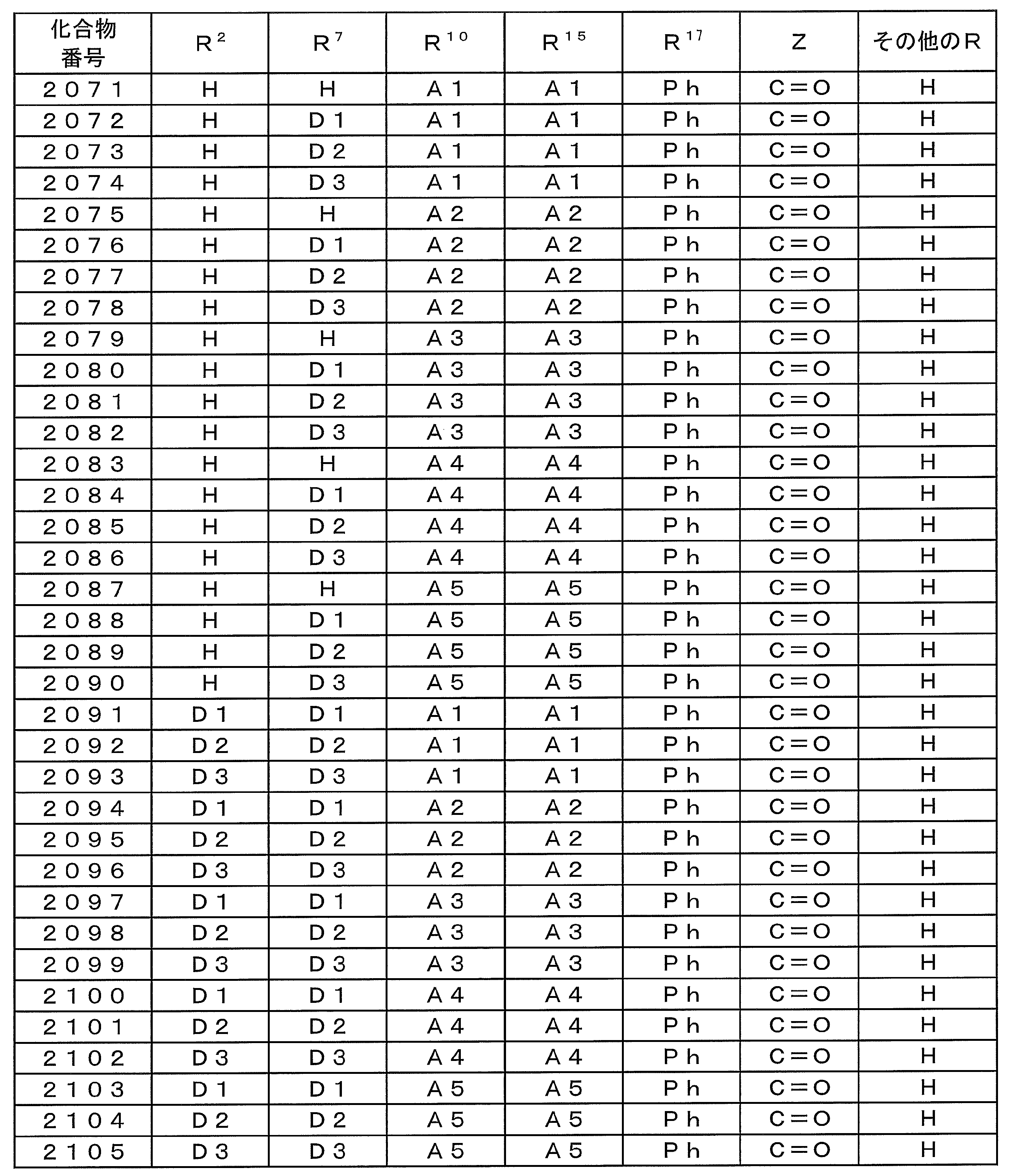
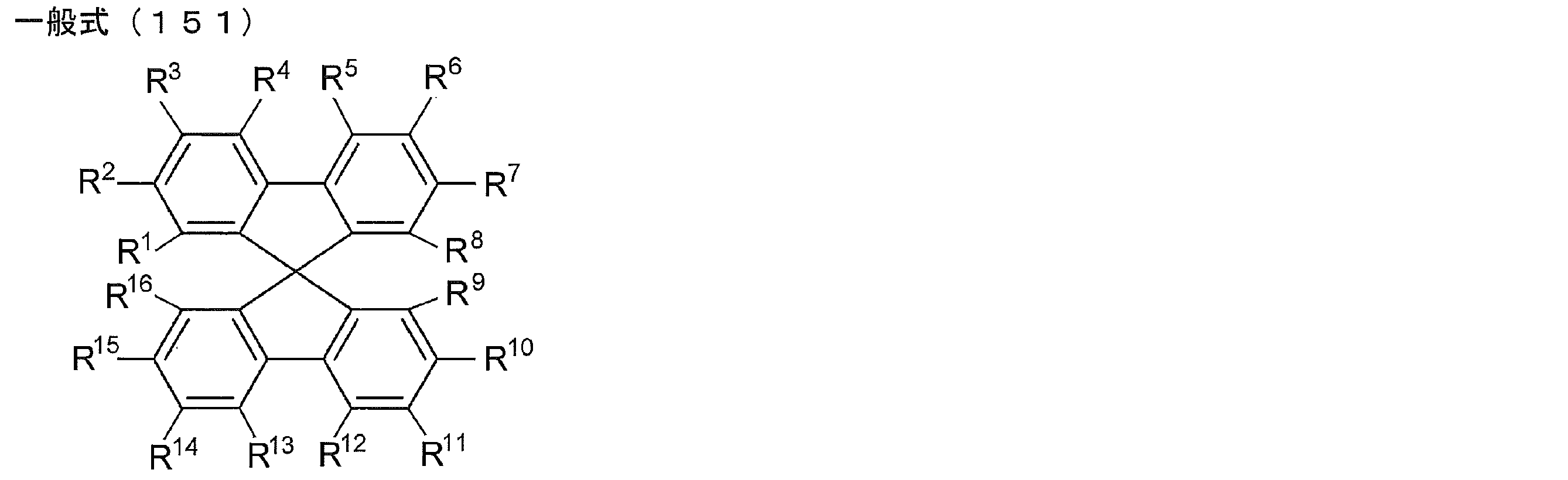
- R 1 , R 2 , R 3 , R 4 , R 5 , R 6 , R 7 , R 8 and R 17 are each independently a hydrogen atom or an electron donating group, One represents an electron donating group.
- R 9 , R 10 , R 11 , R 12 , R 13 , R 14 , R 15 and R 16 are each independently a hydrogen atom or an electron withdrawing group having no unshared electron pair at the ⁇ -position.
- Z is a single bond, at least one of R 9 , R 10 , R 11 , R 12 , R 13 , R 14 , R 15 and R 16 does not have an unshared electron pair at the ⁇ -position. It is a group. ]
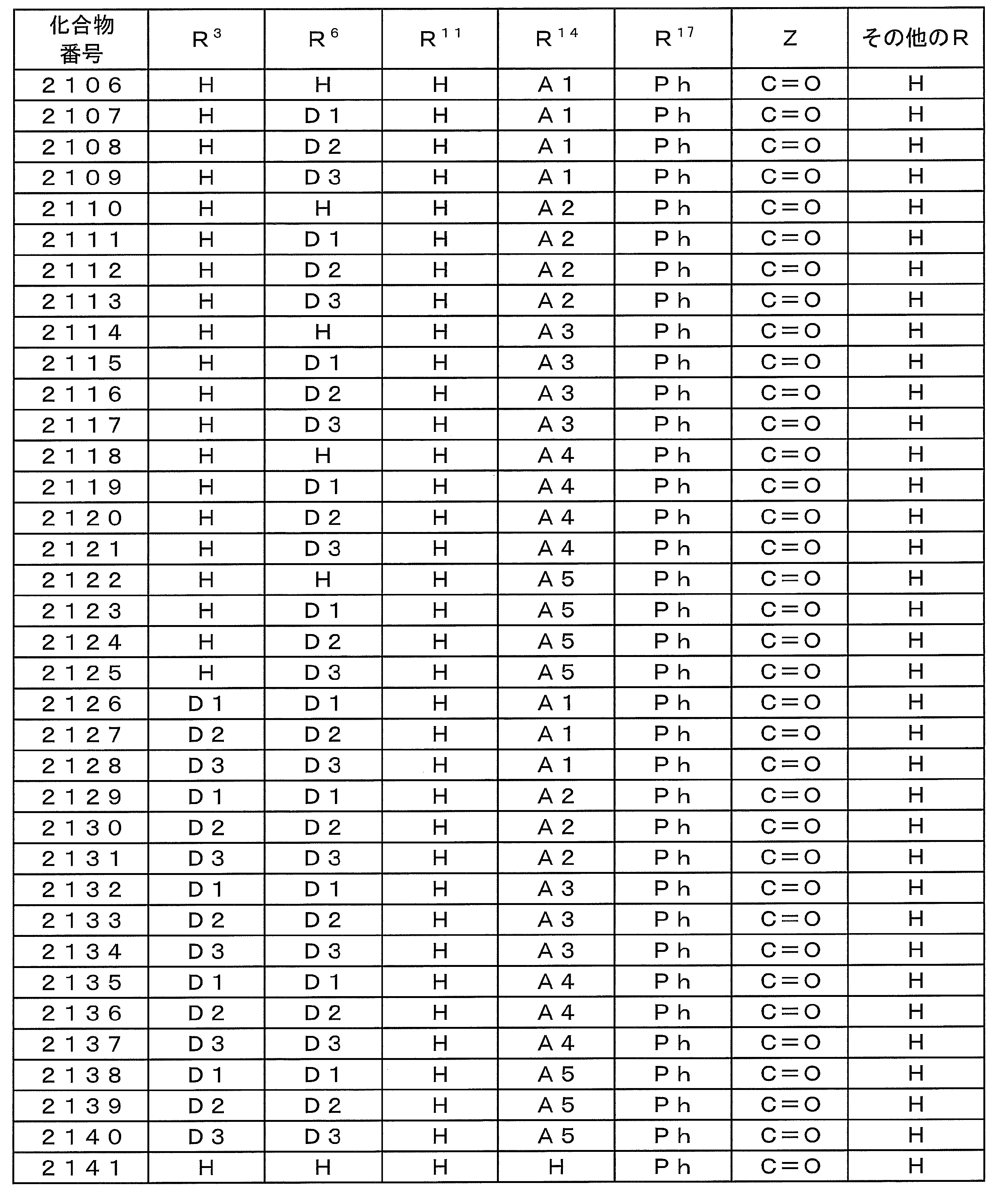
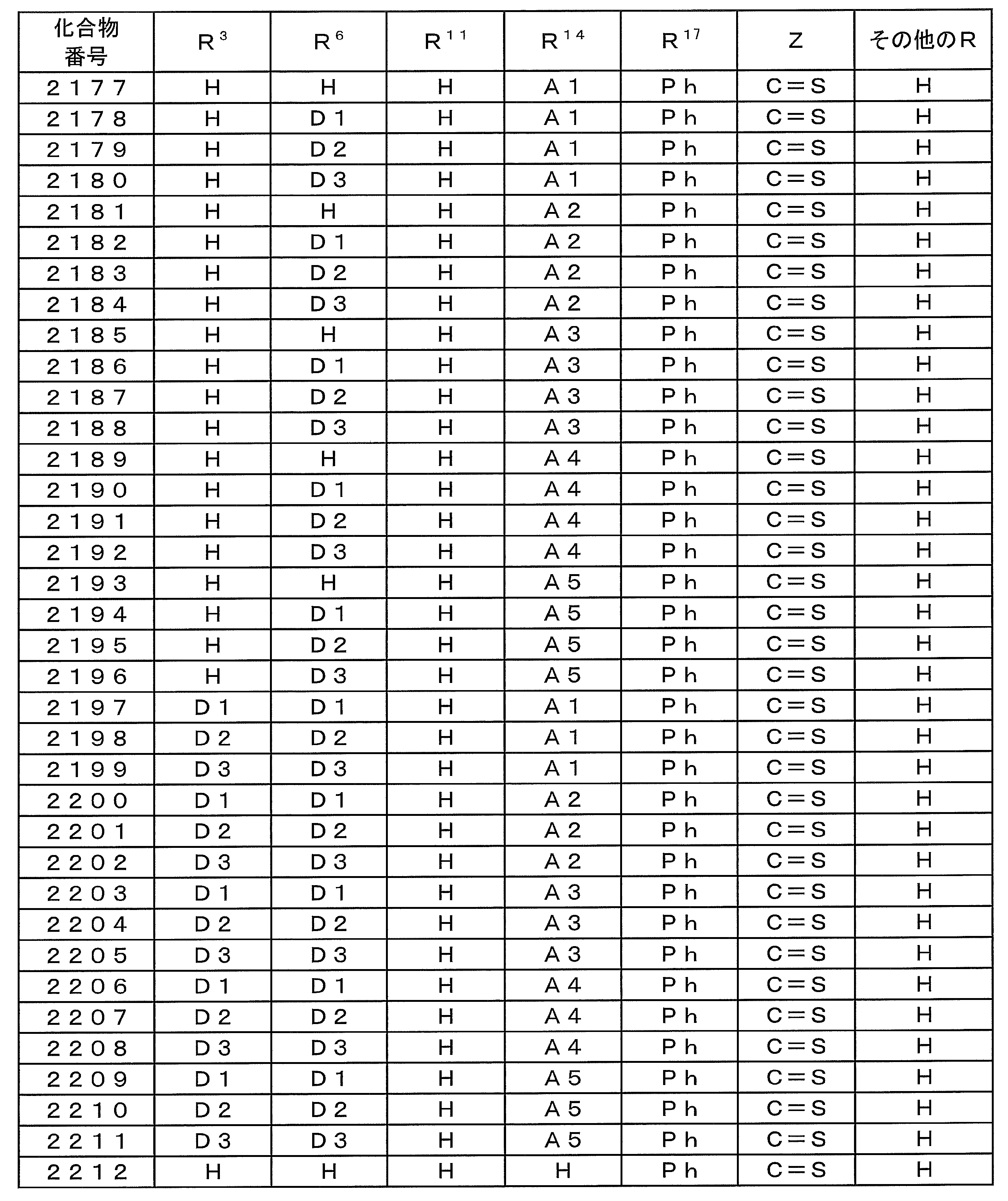
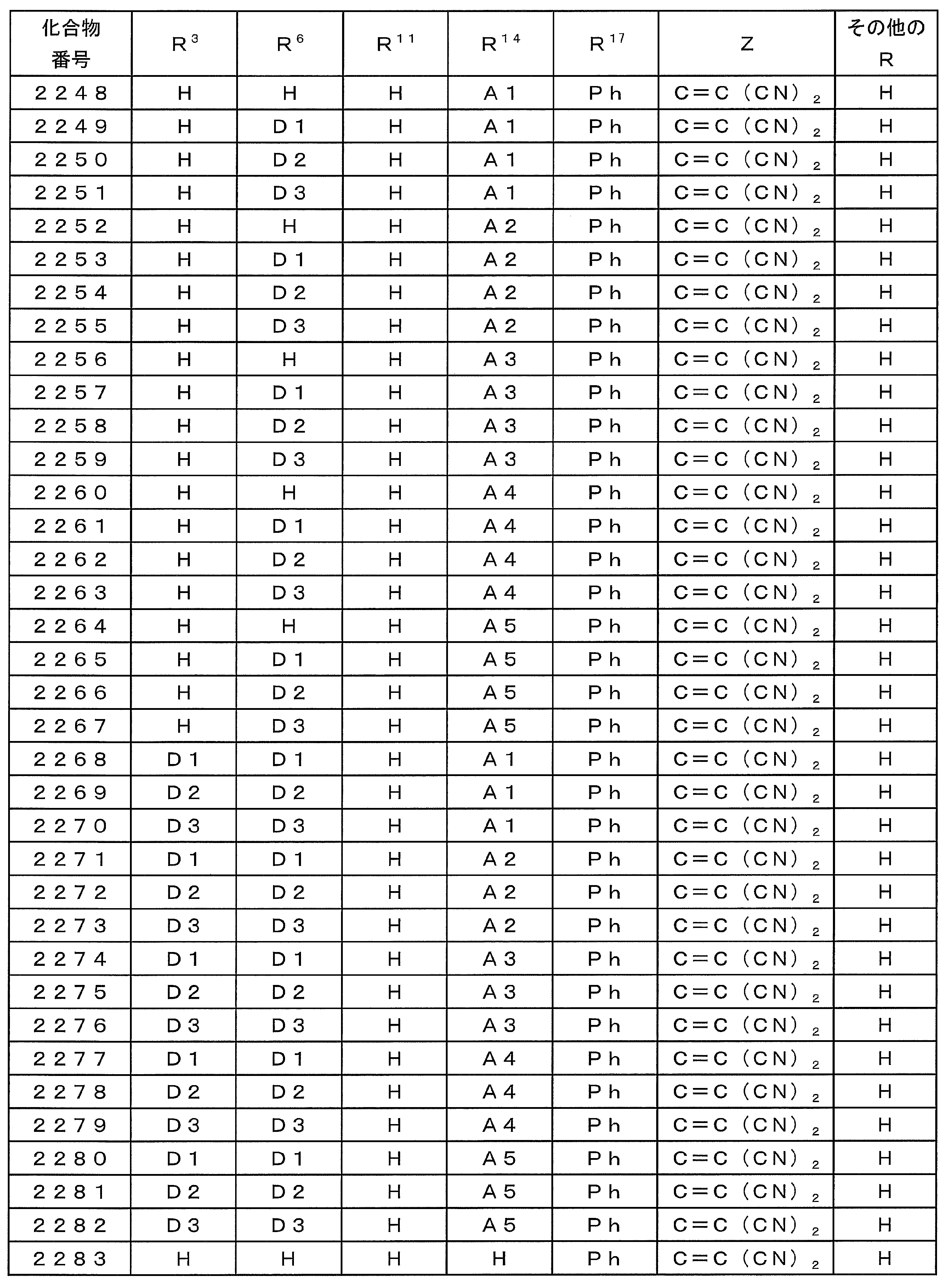
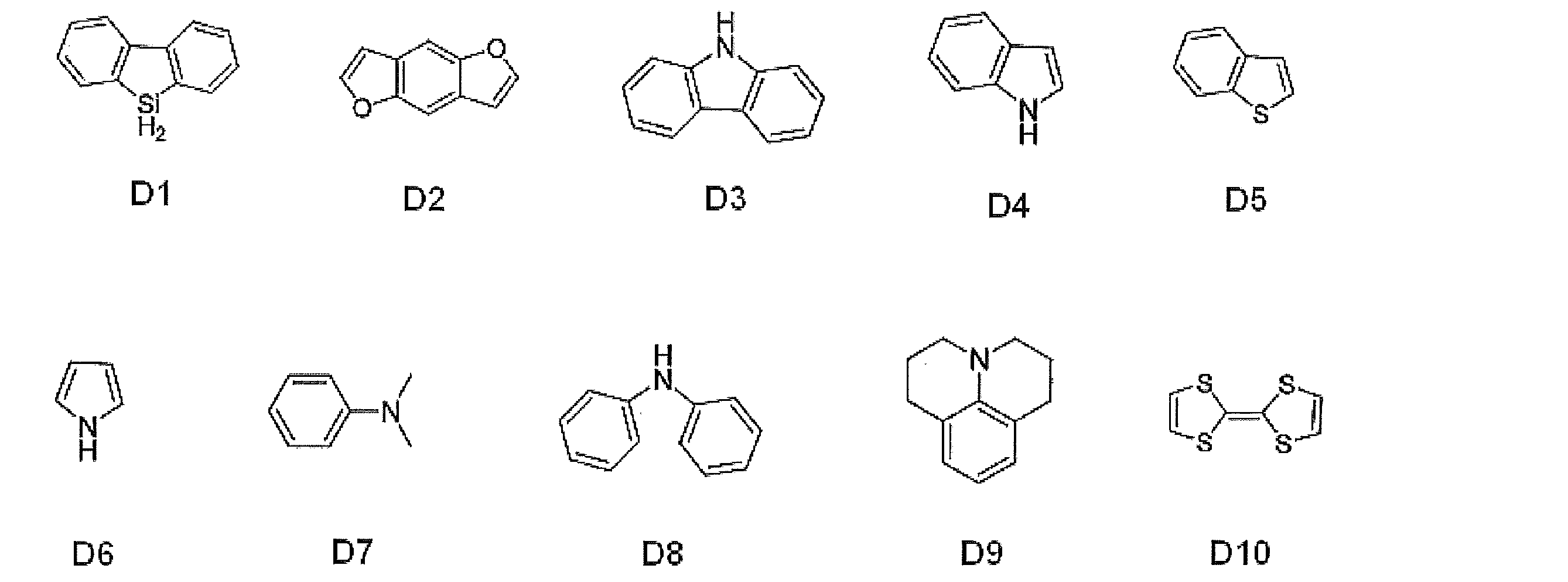
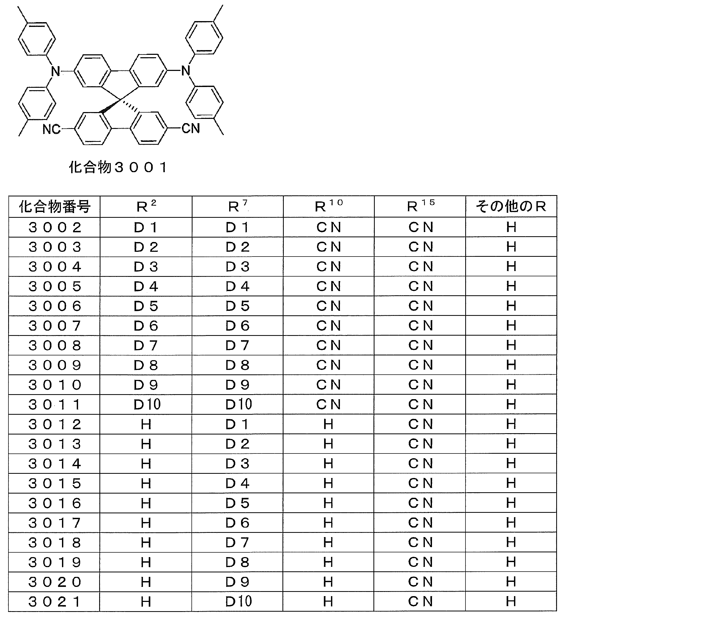
- D1 to D3 represent aryl groups substituted with the following electron donating groups
- A1 to A5 represent the following electron withdrawing groups
- H represents a hydrogen atom
- Ph represents a phenyl group.
- Preferred examples of the luminescent material that can emit delayed fluorescence include compounds represented by the following general formula.
- the entire specification of the publication including the descriptions of paragraphs 0007 to 0033 and 0059 to 0066 of WO 2013/011955 is cited herein as a part of the specification of the present application.
- R 1 , R 2 , R 3 , R 4 , R 5 , R 6 , R 7 and R 8 are each independently a hydrogen atom or an electron-donating group, and at least one of Represents an electron donating group.
- R 9 , R 10 , R 11 , R 12 , R 13 , R 14 , R 15 and R 16 are each independently a hydrogen atom or an electron withdrawing group, and at least one represents an electron withdrawing group.
- D1 to D10 represent unsubstituted electron donating groups having the following skeleton.
- any one of Y 1 , Y 2 and Y 3 represents a nitrogen atom and the remaining one represents a methine group, or all of Y 1 , Y 2 and Y 3 represent a nitrogen atom.
- Z 1 and Z 2 each independently represent a hydrogen atom or a substituent.
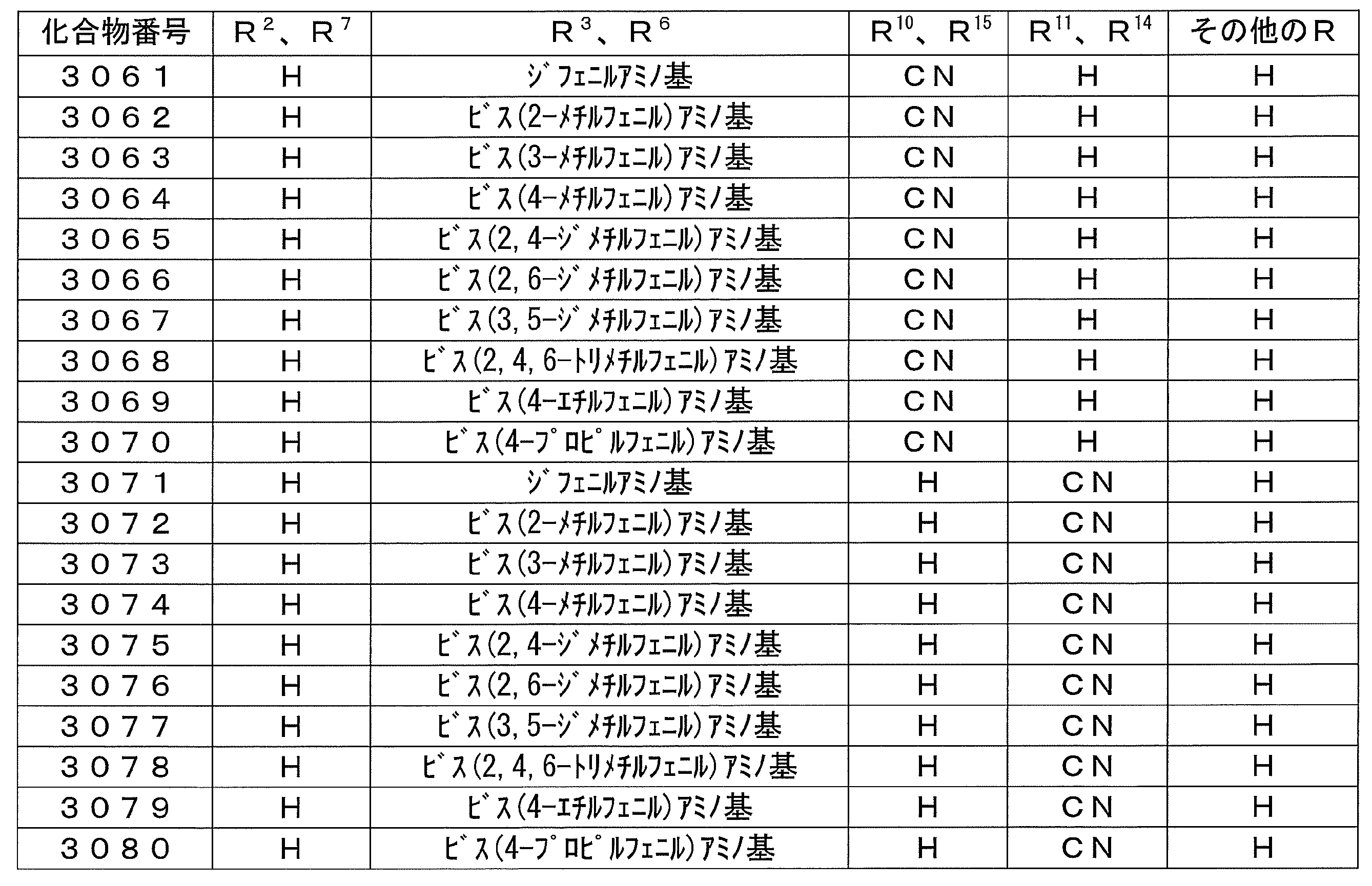
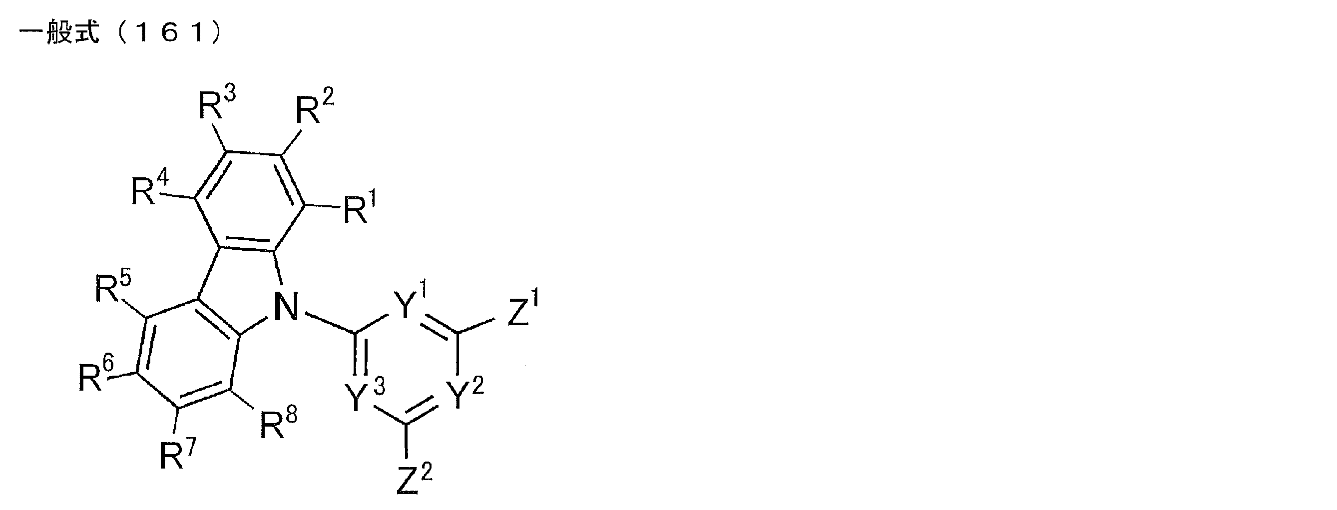
- R 1 to R 8 each independently represents a hydrogen atom or a substituent, and at least one of R 1 to R 8 represents a substituted or unsubstituted diarylamino group or a substituted or unsubstituted carbazolyl group.
- the compound represented by the general formula (161) includes at least two carbazole structures in the molecule.
- Preferred examples of the luminescent material that can emit delayed fluorescence include compounds represented by the following general formula. Further, the entire specification of the publication including paragraphs 0009 to 0046 and 0093 to 0134 of JP2013-256490A is cited herein as a part of the specification of the present application.
- Ar 1 to Ar 3 each independently represents a substituted or unsubstituted aryl group, and at least one represents an aryl group substituted with a group represented by the following general formula (172) .
- R 1 to R 8 each independently represents a hydrogen atom or a substituent.
- Z represents O, S, O ⁇ C or Ar 4 —N
- Ar 4 represents a substituted or unsubstituted aryl group.
- R 1 and R 2 , R 2 and R 3 , R 3 and R 4 , R 5 and R 6 , R 6 and R 7 , R 7 and R 8 may be bonded to each other to form a cyclic structure. Good. ]
- Preferred examples of the luminescent material that can emit delayed fluorescence include compounds represented by the following general formula.
- the entire specification of the gazette including paragraphs 0008 to 0020 and 0038 to 0040 of JP 2013-116975 A is cited herein as a part of the specification of the present application.
- R 1 , R 2 , R 4 to R 8 , R 11 , R 12 and R 14 to R 18 each independently represent a hydrogen atom or a substituent.
- Examples of preferable luminescent materials that can emit delayed fluorescence include the following compounds.
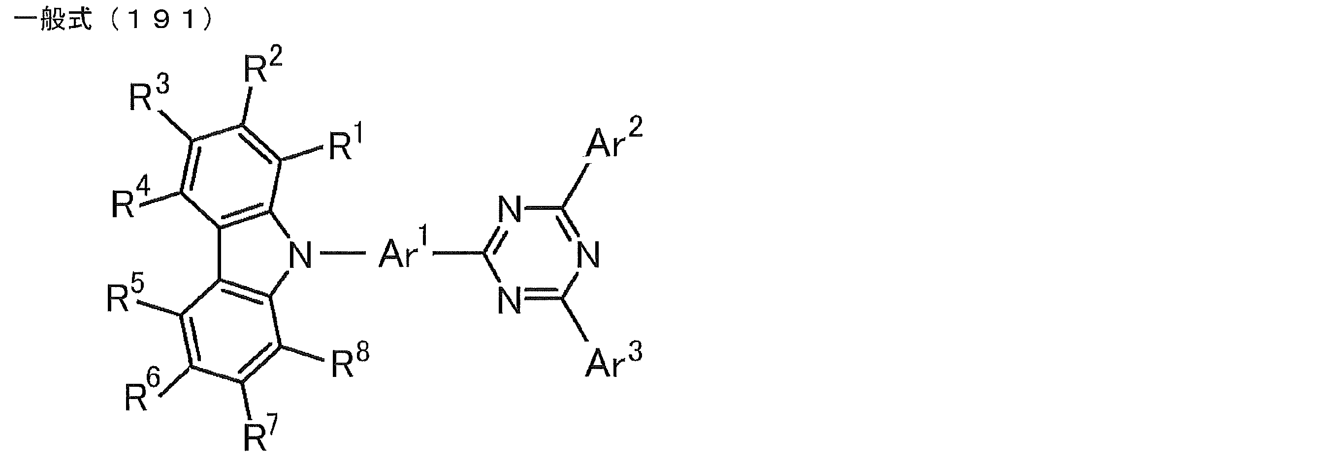
- a compound represented by the following general formula (191) Ar 1 represents a substituted or unsubstituted arylene group, and Ar 2 and Ar 3 each independently represent a substituted or unsubstituted aryl group.
- R 1 to R 8 each independently represents a hydrogen atom or a substituent, and at least one of R 1 to R 8 is a substituted or unsubstituted diarylamino group.
- R 1 and R 2 , R 2 and R 3 , R 3 and R 4 , R 5 and R 6 , R 6 and R 7 , R 7 and R 8 may be bonded to each other to form a cyclic structure. Good.
- At least one of R 1 to R 4 in the general formula (191) is a substituted or unsubstituted diarylamino group, and at least one of R 5 to R 8 is a substituted or unsubstituted diarylamino group
- R 3 and R 6 in the general formula (191) are a substituted or unsubstituted diarylamino group.
- R 1 to R 8 and R 11 to R 24 each independently represent a hydrogen atom or a substituent, and at least one of R 1 to R 8 is a substituted or unsubstituted diarylamino group It is.
- R 1 and R 2 , R 2 and R 3 , R 3 and R 4 , R 5 and R 6 , R 6 and R 7 , R 7 and R 8 , R 11 and R 12 , R 12 and R 13 , R 13 And R 14 , R 14 and R 15 , R 16 and R 17 , R 17 and R 18 , R 18 and R 19 , R 19 and R 20 , R 21 and R 22 , R 23 and R 24 are bonded to each other.
- a ring structure may be formed.
- At least one of R 1 to R 4 in the general formula (192) is a substituted or unsubstituted diarylamino group, and at least one of R 5 to R 8 is a substituted or unsubstituted diarylamino group [7] The compound according to [7]. [9] The compound according to [8], wherein R 3 and R 6 in the general formula (192) are substituted or unsubstituted diarylamino groups.
- Ph represents a phenyl group.
- Examples of preferable luminescent materials that can emit delayed fluorescence include the following compounds.
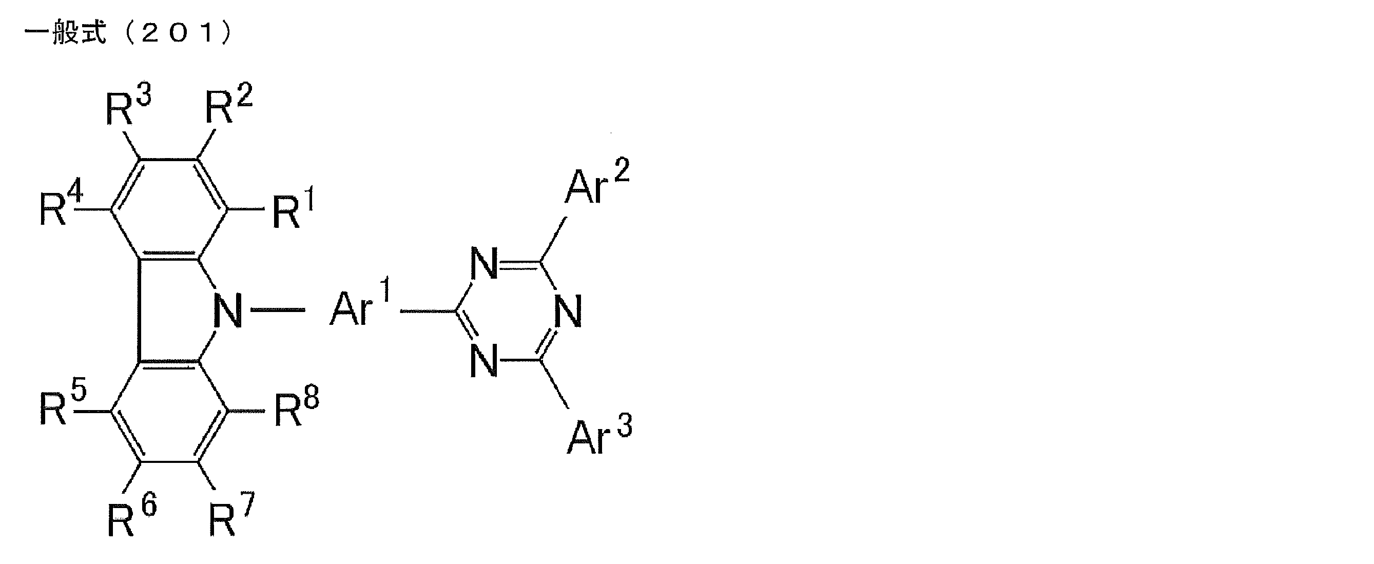
- a compound represented by the following general formula (201). wherein R 1 to R 8 each independently represents a hydrogen atom or a substituent, at least one of R 1 to R 8 is a substituted or unsubstituted carbazolyl group.
- Ar 1 to Ar 3 each represents Independently represents a substituted or unsubstituted aromatic or heteroaromatic ring.
- Preferred examples of the luminescent material that can emit delayed fluorescence include compounds represented by the following general formula.
- the entire specification of the publication including the descriptions of paragraphs 0007 to 0032 and 0079 to 0084 of WO 2013/133359 is cited herein as a part of the specification of the present application.
- Z 1 , Z 2 and Z 3 each independently represent a substituent.
- Ar 1 , Ar 2 , Ar 3 , Ar 4 , Ar 5 and Ar 6 each independently represent a substituted or unsubstituted aryl group.
- Ar 1 , Ar 2 , Ar 3 , Ar 4 , Ar 5, and Ar 6 are all the same, and are collectively referred to as Ar.
- R 1 to R 10 each independently represents a hydrogen atom or a substituent, and at least one of R 1 to R 10 is a substituted or unsubstituted aryl group, substituted or unsubstituted A substituted diarylamino group, or a substituted or unsubstituted 9-carbazolyl group.
- R 1 and R 2 , R 2 and R 3 , R 3 and R 4 , R 4 and R 5 , R 5 and R 6 , R 6 and R 7 , R 7 and R 8 , R 8 and R 9 , R 9 And R 10 may be bonded to each other to form a cyclic structure.
- R 1 to R 4 each independently represents a hydrogen atom or a substituted or unsubstituted (N, N-diarylamino) aryl group, and at least one of R 1 to R 4 is substituted or It represents an unsubstituted (N, N-diarylamino) aryl group.
- Two aryl groups constituting the diarylamino part of the (N, N-diarylamino) aryl group may be linked to each other.
- W 1 , W 2 , X 1 , X 2 , Y 1 , Y 2 , Z 1 and Z 2 each independently represent a carbon atom or a nitrogen atom.
- m 1 to m 4 each independently represents 0, 1 or 2.
- R 1 to R 6 each independently represents a hydrogen atom or a substituent, and at least one of R 1 to R 6 represents a substituted or unsubstituted (N, N-diarylamino) aryl group Represents. Two aryl groups constituting the diarylamino part of the (N, N-diarylamino) aryl group may be linked to each other.
- X 1 to X 6 and Y 1 to Y 6 each independently represent a carbon atom or a nitrogen atom.
- n 1 , n 2 , p 1 , p 2 , q 1 and q 2 each independently represents 0, 1 or 2.
- a plurality of light emitting materials are used for the organic electroluminescence device of the present invention. Those light emitting materials may be contained together in one light emitting layer, or may be individually contained in different light emitting layers. In the organic electroluminescence device of the present invention, a light emitting layer containing two or more light emitting materials and a light emitting layer containing a single light emitting material may be mixed.
- the two types of light emitting materials include a combination of a blue light emitting material and a red light emitting material, a combination of a blue light emitting material and a green light emitting material, and the like, but are not limited thereto.
- the blue light-emitting material that emits light having a short wavelength is required to be at least a delayed fluorescent material.
- “1” indicates a light emitting material that emits light having the shortest emission wavelength
- “2” indicates a light emitting material that emits light having a longer wavelength.
- a numeral written in the circle indicates that the light emitting material corresponding to the numeral is doped.
- the left mold shows the anode side
- the right mold shows the cathode side.
- the (1-1) type in FIG. 2 includes only the blue light-emitting material from the anode side. It shows that the layers are formed in the order of the light emitting layer and the light emitting layer made of only the red light emitting material.
- the (1-2) type shows a mode in which a red light emitting material is doped into a blue light emitting material in a single light emitting layer.
- the blue light emitting material functions as a light emitting material that emits fluorescence including delayed fluorescence, and also functions as a host of the red light emitting material.
- the (1-3) type and the (1-4) type show a mode in which a light emitting layer made of only a blue light emitting material and a light emitting layer doped with a red light emitting material in a blue light emitting material are stacked.
- the (1-5) type shows a mode in which a light emitting layer doped with a red light emitting material is sandwiched between two light emitting layers made of only a blue light emitting material.
- 3 to 6 show configuration examples of the light-emitting layer when three types of light-emitting materials are used.
- the three types of light emitting materials include, but are not limited to, combinations of blue light emitting materials, green light emitting materials, and red light emitting materials.
- the blue light-emitting material that emits light having the shortest wavelength is required to be at least a delayed fluorescent material.
- “1” indicates a light emitting material that emits light with the shortest emission wavelength
- “2” indicates a light emitting material that emits light with the next shortest wavelength
- “3” indicates light with the longest wavelength.
- the luminescent material to be emitted is shown.
- a numeral written in the circle indicates that the light emitting material corresponding to the numeral is doped.
- the left mold shows the anode side
- the right mold shows the cathode side.
- the (3-1) to (3-4) types are embodiments having a light emitting layer containing all three types of light emitting materials. That is, in the case of the (3-1) type, for example, a blue light emitting material functions as a light emitting material that emits fluorescence including delayed fluorescence, and also functions as a host of green light emitting material and red light emitting material.
- the types (4-1) to (4-14) include a light emitting layer in which a light emitting material “1” is doped with a light emitting material “2”, and a light emitting material “3” in a light emitting material “1”.
- Types (5-1) to (5-9) are embodiments having a light emitting layer in which a light emitting material of “2” is doped with a light emitting material of “3” and a light emitting layer containing “1” alone. .
- the light emitting layer closest to the cathode and the light emitting layer closest to the anode are both layers made of a light emitting material that emits light at the shortest wavelength. It is possible.
- a light-emitting layer containing a light-emitting material that emits light at the shortest wavelength as a host material can be disposed between the light-emitting layer closest to the cathode and the light-emitting layer closest to the anode.
- the concentration when the light emitting material is doped in the light emitting layer is preferably 0.01% by weight or more, more preferably 0.1% by weight or more, and preferably 50% by weight or less, More preferably, it is 20 weight% or less, More preferably, it is 10 weight% or less, For example, it can be 1 weight% or less.
- the host material may not be the above light emitting material. That is, a host material used for a normal light emitting material can be appropriately selected and used.
- the organic electroluminescent device and the organic photoluminescent device of the present invention In order for the organic electroluminescent device and the organic photoluminescent device of the present invention to exhibit high luminous efficiency, it is important to confine singlet excitons and triplet excitons generated in the light emitting material in the light emitting material.
- the host material an organic compound having a higher value than the light emitting material doped with at least one of excited singlet energy and excited triplet energy can be used.
- singlet excitons and triplet excitons generated in the light emitting material can be confined in the molecule of the light emitting material, and the light emission efficiency can be sufficiently extracted.
- the host material is preferably an organic compound which has a hole transporting ability and an electron transporting ability, prevents emission of longer wavelengths, and has a high glass transition temperature.
- the light emission intensity from the light emitting material that emits light at the shortest wavelength is preferably 20% or more, more preferably 25% or more, and more preferably 30% or more. Is more preferable.
- the blue emission intensity is preferably 20% or more of the total emission, more preferably 25% or more, and further preferably 30% or more.
- the organic electroluminescence device of the present invention has a structure in which an organic layer is formed at least between an anode, a cathode, and an anode and a cathode.
- the organic layer includes at least a light emitting layer, and may consist of only the light emitting layer, or may have one or more organic layers in addition to the light emitting layer. Examples of such other organic layers include a hole transport layer, a hole injection layer, an electron blocking layer, a hole blocking layer, an electron injection layer, an electron transport layer, and an exciton blocking layer.
- the hole transport layer may be a hole injection / transport layer having a hole injection function
- the electron transport layer may be an electron injection / transport layer having an electron injection function.
- a specific structure example of the organic electroluminescence element is shown in FIG. In FIG. 7, 1 is a substrate, 2 is an anode, 3 is a hole injection layer, 4 is a hole transport layer, 5 is a light emitting layer, 6 is an electron transport layer, 7 is an electron injection layer, and 8 is a cathode. Below, each member and each layer of an organic electroluminescent element are demonstrated. Note that the above description can be referred to for the light emitting layer.
- the organic electroluminescence device of the present invention is preferably supported on a substrate.
- the substrate is not particularly limited and may be any substrate conventionally used for organic electroluminescence elements.
- a substrate made of glass, transparent plastic, quartz, silicon, or the like can be used.
- an electrode material made of a metal, an alloy, an electrically conductive compound, or a mixture thereof having a high work function (4 eV or more) is preferably used.
- electrode materials include metals such as Au, and conductive transparent materials such as CuI, indium tin oxide (ITO), SnO 2 , and ZnO.
- conductive transparent materials such as CuI, indium tin oxide (ITO), SnO 2 , and ZnO.
- an amorphous material such as IDIXO (In 2 O 3 —ZnO) that can form a transparent conductive film may be used.
- a thin film may be formed by vapor deposition or sputtering of these electrode materials, and a pattern of a desired shape may be formed by photolithography, or when pattern accuracy is not so high (about 100 ⁇ m or more) ), A pattern may be formed through a mask having a desired shape at the time of vapor deposition or sputtering of the electrode material.
- wet film-forming methods such as a printing system and a coating system, can also be used.
- the transmittance be greater than 10%, and the sheet resistance as the anode is preferably several hundred ⁇ / ⁇ or less.
- the film thickness depends on the material, it is usually selected in the range of 10 to 1000 nm, preferably 10 to 200 nm.
- cathode a material having a low work function (4 eV or less) metal (referred to as an electron injecting metal), an alloy, an electrically conductive compound, and a mixture thereof as an electrode material is used.
- electrode materials include sodium, sodium-potassium alloy, magnesium, lithium, magnesium / copper mixture, magnesium / silver mixture, magnesium / aluminum mixture, magnesium / indium mixture, aluminum / aluminum oxide (Al 2 O 3 ) Mixtures, indium, lithium / aluminum mixtures, rare earth metals and the like.
- a mixture of an electron injecting metal and a second metal which is a stable metal having a larger work function value than this for example, a magnesium / silver mixture
- Suitable are a magnesium / aluminum mixture, a magnesium / indium mixture, an aluminum / aluminum oxide (Al 2 O 3 ) mixture, a lithium / aluminum mixture, aluminum and the like.
- the cathode can be produced by forming a thin film of these electrode materials by a method such as vapor deposition or sputtering.
- the sheet resistance as the cathode is preferably several hundred ⁇ / ⁇ or less, and the film thickness is usually selected in the range of 10 nm to 5 ⁇ m, preferably 50 to 200 nm.
- the emission luminance is advantageously improved.
- a transparent or semi-transparent cathode can be produced. By applying this, an element in which both the anode and the cathode are transparent is used. Can be produced.
- the injection layer is a layer provided between the electrode and the organic layer for lowering the driving voltage and improving the luminance of light emission.
- the injection layer can be provided as necessary.
- the blocking layer is a layer that can prevent diffusion of charges (electrons or holes) and / or excitons existing in the light emitting layer to the outside of the light emitting layer.
- the electron blocking layer can be disposed between the light emitting layer and the hole transport layer and blocks electrons from passing through the light emitting layer toward the hole transport layer.
- a hole blocking layer can be disposed between the light emitting layer and the electron transporting layer to prevent holes from passing through the light emitting layer toward the electron transporting layer.
- the blocking layer can also be used to block excitons from diffusing outside the light emitting layer. That is, each of the electron blocking layer and the hole blocking layer can also function as an exciton blocking layer.
- the term “electron blocking layer” or “exciton blocking layer” as used herein is used in the sense of including a layer having the functions of an electron blocking layer and an exciton blocking layer in one layer.
- the hole blocking layer has a function of an electron transport layer in a broad sense.
- the hole blocking layer has a role of blocking holes from reaching the electron transport layer while transporting electrons, thereby improving the recombination probability of electrons and holes in the light emitting layer.
- the material for the hole blocking layer the material for the electron transport layer described later can be used as necessary.
- the electron blocking layer has a function of transporting holes in a broad sense.
- the electron blocking layer has a role to block electrons from reaching the hole transport layer while transporting holes, thereby improving the probability of recombination of electrons and holes in the light emitting layer. .
- the exciton blocking layer is a layer for preventing excitons generated by recombination of holes and electrons in the light emitting layer from diffusing into the charge transport layer. It becomes possible to efficiently confine in the light emitting layer, and the light emission efficiency of the device can be improved.
- the exciton blocking layer can be inserted on either the anode side or the cathode side adjacent to the light emitting layer, or both can be inserted simultaneously.
- the layer when the exciton blocking layer is provided on the anode side, the layer can be inserted adjacent to the light emitting layer between the hole transport layer and the light emitting layer, and when inserted on the cathode side, the light emitting layer and the cathode Between the luminescent layer and the light-emitting layer.
- a hole injection layer, an electron blocking layer, or the like can be provided between the anode and the exciton blocking layer adjacent to the anode side of the light emitting layer, and the excitation adjacent to the cathode and the cathode side of the light emitting layer can be provided.
- an electron injection layer, an electron transport layer, a hole blocking layer, and the like can be provided.
- the blocking layer is disposed, at least one of the excited singlet energy and the excited triplet energy of the material used as the blocking layer is preferably higher than the excited singlet energy and the excited triplet energy of the light emitting material.
- the hole transport layer is made of a hole transport material having a function of transporting holes, and the hole transport layer can be provided as a single layer or a plurality of layers.
- the hole transport material has any one of hole injection or transport and electron barrier properties, and may be either organic or inorganic.
- hole transport materials that can be used include, for example, triazole derivatives, oxadiazole derivatives, imidazole derivatives, carbazole derivatives, indolocarbazole derivatives, polyarylalkane derivatives, pyrazoline derivatives and pyrazolone derivatives, phenylenediamine derivatives, arylamine derivatives, Examples include amino-substituted chalcone derivatives, oxazole derivatives, styrylanthracene derivatives, fluorenone derivatives, hydrazone derivatives, stilbene derivatives, silazane derivatives, aniline copolymers, and conductive polymer oligomers, particularly thiophene oligomers.
- An aromatic tertiary amine compound and an styrylamine compound are preferably used, and an aromatic tertiary amine compound is more preferably used.
- the electron transport layer is made of a material having a function of transporting electrons, and the electron transport layer can be provided as a single layer or a plurality of layers.
- the electron transport material (which may also serve as a hole blocking material) may have a function of transmitting electrons injected from the cathode to the light emitting layer.
- Examples of the electron transport layer that can be used include nitro-substituted fluorene derivatives, diphenylquinone derivatives, thiopyran dioxide oxide derivatives, carbodiimides, fluorenylidenemethane derivatives, anthraquinodimethane and anthrone derivatives, oxadiazole derivatives, and the like.
- a thiadiazole derivative in which the oxygen atom of the oxadiazole ring is substituted with a sulfur atom, and a quinoxaline derivative having a quinoxaline ring known as an electron withdrawing group can also be used as an electron transport material.
- a polymer material in which these materials are introduced into a polymer chain or these materials are used as a polymer main chain can also be used.
- the compound represented by the general formula (1) may be used not only for the light emitting layer but also for layers other than the light emitting layer.
- the compound represented by General formula (1) used for a light emitting layer and the compound represented by General formula (1) used for layers other than a light emitting layer may be same or different.
- the compound represented by the general formula (1) may be used for the injection layer, blocking layer, hole blocking layer, electron blocking layer, exciton blocking layer, hole transporting layer, electron transporting layer, and the like. .
- the method for forming these layers is not particularly limited, and the layer may be formed by either a dry process or a wet process.
- the preferable material which can be used for an organic electroluminescent element is illustrated concretely.
- the material that can be used in the present invention is not limited to the following exemplary compounds.
- R, R ′, and R 1 to R 10 each independently represent a hydrogen atom or a substituent.
- X represents a carbon atom or a hetero atom forming a ring skeleton
- n represents an integer of 3 to 5
- Y represents a substituent
- m represents an integer of 0 or more.
- the organic electroluminescence device produced by the above method emits light by applying an electric field between the anode and the cathode of the obtained device. At this time, if the light is emitted by excited singlet energy, light having a wavelength corresponding to the energy level is confirmed as fluorescence emission and delayed fluorescence emission. In addition, in the case of light emission by excited triplet energy, a wavelength corresponding to the energy level is confirmed as phosphorescence. Since normal fluorescence has a shorter fluorescence lifetime than delayed fluorescence, the emission lifetime can be distinguished from fluorescence and delayed fluorescence.
- the organic electroluminescence element of the present invention can be applied to any of a single element, an element having a structure arranged in an array, and a structure in which an anode and a cathode are arranged in an XY matrix. According to the present invention, an organic light emitting device with greatly improved luminous efficiency can be obtained.
- the organic light emitting device such as the organic electroluminescence device of the present invention can be further applied to various uses. For example, it is possible to produce an organic electroluminescence display device using the organic electroluminescence element of the present invention. For details, see “Organic EL Display” (Ohm Co., Ltd.) ) Can be referred to.
- the organic electroluminescence device of the present invention can be applied to organic electroluminescence illumination and backlights that are in great demand.
- the maximum point having a peak intensity of 10% or less of the maximum peak intensity of the spectrum is not included in the above-mentioned maximum value on the shortest wavelength side, and has the maximum slope value closest to the maximum value on the shortest wavelength side.
- the tangent drawn at the point where the value was taken was taken as the tangent to the rising edge of the phosphorescence spectrum on the short wavelength side.
- Example 1 a multi-wavelength light emitting organic electroluminescence element in which three light emitting materials of a blue light emitting material, a green light emitting material, and a red light emitting material were mixed in one light emitting layer was manufactured and evaluated.
- Each thin film was laminated at a vacuum degree of 5.0 ⁇ 10 ⁇ 4 Pa by a vacuum deposition method on a glass substrate on which an anode made of indium tin oxide (ITO) having a thickness of 100 nm was formed.
- ITO indium tin oxide
- ⁇ -NPD was formed on ITO to a thickness of 35 nm
- mCBP was formed to a thickness of 10 nm.
- a blue light emitting material ZHS02, a green light emitting material 4CzIPN, and a red light emitting material 4CzTPN-Ph were co-evaporated from different vapor deposition sources to form a 15 nm thick layer as a light emitting layer.
- concentrations of 4CzIPN and 4CzTPN-Ph were 0.1% by weight, respectively, and the remainder was ZHS02.
- PPT is formed to a thickness of 10 nm
- TPBi is formed to a thickness of 40 nm
- lithium fluoride (LiF) is vacuum-deposited to 0.8 nm
- aluminum (Al) is deposited to a thickness of 100 nm.
- FIG. 8 shows the emission spectrum of the produced organic electroluminescence device
- FIG. 9 shows the current density-external quantum efficiency characteristics
- FIG. 10 shows the energy band diagram.
- Table 2 shows the external quantum efficiency and chromaticity.
- the emission intensity ratio was 32% for blue light emission, 49% for green light emission, and 19% for red light emission.
- the blue delayed fluorescence increased the intensity ratio of blue light emission, and both good blueness and high light emission efficiency could be achieved.
- Example 2 to 4 a multi-wavelength light emitting organic electroluminescence element in which two light emitting materials of a blue light emitting material and a red light emitting material were mixed in three concentrations in one light emitting layer was manufactured and evaluated.
- Each thin film was laminated at a vacuum degree of 5.0 ⁇ 10 ⁇ 4 Pa by a vacuum deposition method on a glass substrate on which an anode made of indium tin oxide (ITO) having a thickness of 100 nm was formed.
- ITO indium tin oxide
- ⁇ -NPD was formed on ITO to a thickness of 35 nm
- mCBP was formed to a thickness of 10 nm.
- a blue light emitting material, 2CzPN, and a red light emitting material, 4CzTPN-Ph were co-evaporated from different vapor deposition sources to form a 15 nm thick layer as a light emitting layer.
- the concentration of 4CzTPN-Ph was 0.1% by weight (Example 2), 0.2% by weight (Example 3), and 0.5% by weight (Example 4).
- TmPyPb is formed to a thickness of 50 nm
- lithium fluoride (LiF) is vacuum-deposited to a thickness of 0.8 nm
- aluminum (Al) is evaporated to a thickness of 100 nm to form a cathode.
- a luminescence element was obtained.
- the emission spectrum of the produced organic electroluminescence device is shown in FIG. 11, the current density-external quantum efficiency characteristic is shown in FIG. 12, and the energy band diagram is shown in FIG.
- the external quantum efficiency and chromaticity are as shown in Table 2, and it was possible to achieve both good blueness and high luminous efficiency.
- Example 5 a multi-wavelength light-emitting organic electroluminescence element having a structure in which a light-emitting layer composed of only a blue light-emitting material and a light-emitting layer doped with a red light-emitting material sandwiched between blue light-emitting materials was fabricated and evaluated. Each thin film was laminated at a vacuum degree of 5.0 ⁇ 10 ⁇ 4 Pa by a vacuum deposition method on a glass substrate on which an anode made of indium tin oxide (ITO) having a thickness of 100 nm was formed.
- ITO indium tin oxide
- ⁇ -NPD was formed on ITO to a thickness of 35 nm
- mCBP was formed to a thickness of 10 nm
- blue light emitting material ZHS02 was formed to 7 nm.
- ZHS02 and 4CzTPN-Ph which is a red light emitting material, were co-evaporated from different vapor deposition sources to form a 1 nm thick layer as a light emitting layer. At this time, the concentration of 4CzTPN-Ph was 0.2% by weight.
- ZHS02 is formed to a thickness of 7 nm
- TmPyPb is formed to a thickness of 50 nm
- lithium fluoride (LiF) is vacuum-deposited to 0.8 nm
- aluminum (Al) is evaporated to a thickness of 100 nm.
- a cathode was formed, and an organic electroluminescence element was obtained.
- the emission spectrum of the produced organic electroluminescence element is shown in FIG. 14, the current density-external quantum efficiency characteristic is shown in FIG. 15, and the energy band diagram is shown in FIG.
- the external quantum efficiency and chromaticity are as shown in Table 2, and it was possible to achieve both good blueness and high luminous efficiency.
- a blue light emitting material, a green light emitting material, and a red light emitting material are all delayed fluorescent materials, and a multi-wavelength light emitting organic electroluminescence element was manufactured and evaluated.
- Each thin film was laminated at a vacuum degree of 5.0 ⁇ 10 ⁇ 4 Pa by a vacuum deposition method on a glass substrate on which an anode made of indium tin oxide (ITO) having a thickness of 100 nm was formed.
- ITO indium tin oxide
- HATCN was formed on ITO to a thickness of 10 nm
- TrisPCz was formed to a thickness of 35 nm.
- TXZ-TRZ and mCBP which are green light emitting materials, were co-evaporated from different vapor deposition sources to form a 6 nm thick layer as the first light emitting layer (the concentration of TXZ-TRZ was 10% by weight).
- TXZ-TRZ, red light emitting material 4CzTPN-Ph and mCBP were co-evaporated from different vapor deposition sources to form a layer having a thickness of 3 nm to form a second light emitting layer (the concentration of TXZ-TRZ was 6).
- the concentration of 4% by weight and 4CzTPN-Ph is 2% by weight).
- SHT02 and DPEPO which are blue light emitting materials, were co-deposited from different vapor deposition sources to form a layer having a thickness of 6 nm to form a third light emitting layer (the concentration of SHT02 was 6% by weight).
- DPEPO was formed to a thickness of 10 nm
- TmPyPb was formed to a thickness of 40 nm.
- lithium fluoride (LiF) was vacuum-deposited at 0.8 nm, and then aluminum (Al) was evaporated at a thickness of 100 nm to form a cathode, whereby an organic electroluminescence element A was obtained (Example 6).
- An organic electroluminescent element B was produced by the same manufacturing method as that of the organic electroluminescent element A, except that a 10 nm thick PPT layer was formed instead of the 10 nm thick DPEPO layer (Example 7). Moreover, the point which did not form 10 nm-thick DPEPO layer was changed, and the organic electroluminescent element C was produced by the manufacturing method similar to the organic electroluminescent element A (Example 8).
- An emission spectrum of the produced organic electroluminescence device A is shown in FIG. The chromaticity was 0.31, 0.36. Further, the voltage-current density characteristics of the produced organic electroluminescence elements A to C are shown in FIG. 18, the current density-external quantum efficiency characteristics are shown in FIG. 19, and the energy band diagram is shown in FIG.
- the organic electroluminescent devices A to C exhibited good light emission characteristics as white light emitting devices, and the organic electroluminescent device A achieved an external quantum efficiency of 11.8%.
- Example 9 In this example, by using another green light emitting material, a multi-wavelength light emitting organic electroluminescence element in which a blue light emitting material, a green light emitting material, and a red light emitting material are all delayed fluorescent materials was manufactured and evaluated.
- 4CzPN instead of PXZ-TRZ as the green light emitting material
- the thicknesses of the first light emitting layer, the second light emitting layer, and the third light emitting layer were changed as follows, and the organic electroluminescent device A of Example 6 was used.
- Organic electroluminescent elements D to F were produced by the same production method as described above.
- Element D 1st light emitting layer (6 nm), 2nd light emitting layer (3 nm), 3rd light emitting layer (6 nm)
- E first light emitting layer (4 nm), second light emitting layer (3 nm), third light emitting layer (8 nm)
- Element F 1st light emitting layer (3 nm), 2nd light emitting layer (2 nm), 3rd light emitting layer (15 nm)
- the emission spectra of the produced organic electroluminescent elements D to F are shown in FIG.
- the chromaticity of the organic electroluminescence element F was 0.30, 0.39.
- the voltage-current density characteristics of the produced organic electroluminescence elements D to F are shown in FIG. 22, and the current density-external quantum efficiency characteristics are shown in FIG.
- the organic electroluminescence element F exhibited good light emission characteristics as a white light emitting element, and achieved an external quantum efficiency of 12.1%.
- the organic electroluminescence device of the present invention is designed so that the light having the shortest wavelength among the light emitted from a plurality of light emitting materials included in the device includes delayed fluorescence. By designing in this way, it is possible to improve the color by increasing the efficiency of light emission having a relatively short wavelength such as blue.
- the organic electroluminescence device of the present invention has a high degree of design freedom, and a desired multi-wavelength light-emitting organic electroluminescence device can be produced with a simple structure. For this reason, this invention has high industrial applicability.
Landscapes
- Physics & Mathematics (AREA)
- Optics & Photonics (AREA)
- Electroluminescent Light Sources (AREA)
Abstract
Description
このような技術状況下において、本発明者らは、青色のように比較的波長が短い発光の効率を上げて色味を改善するとともに、設計上の自由度が大きくて簡易な構造を実現できる多波長発光型の有機エレクトロルミネッセンス素子を提供することを目指して研究を重ねた。
[2] 最も短波長で発光する発光材料が、他の発光材料のホスト材料を兼ねているか、あるいは、単独で有機層を形成していることを特徴とする[1]に記載の有機エレクトロルミネッセンス素子。
[3] 最も短波長で発光する発光材料における、5Kの最低励起三重項エネルギー準位と最低励起一重項エネルギー準位のエネルギー差(ΔEST)が0.3eV以下であることを特徴とする[1]または[2]に記載の有機エレクトロルミネッセンス素子。
[4] 最も短波長で発光する発光材料が青色発光材料であることを特徴とする[1]~[3]のいずれか1項に記載の有機エレクトロルミネッセンス素子。
[5] 最も短波長で発光する発光材料の発光強度が全発光の20%超であることを特徴とする[1]~[4]のいずれか1項に記載の有機エレクトロルミネッセンス素子。
[6] 最も短波長で発光する発光材料とそれ以外の波長で発光する少なくとも1種の発光材料が1つの有機層に含まれており、前記最も短波長で発光する発光材料がホスト材料としても機能することを特徴とする[1]~[5]のいずれか1項に記載の有機エレクトロルミネッセンス素子。
[7] 最も短波長で発光する発光材料とそれ以外の波長で発光する少なくとも2種の発光材料が1つの有機層に含まれており、前記最も短波長で発光する発光材料が発光材料がホスト材料としても機能することを特徴とする[1]~[5]のいずれか1項に記載の有機エレクトロルミネッセンス素子。
[8] 最も短波長で発光する発光材料が、単独で少なくとも1層の有機層を形成していることを特徴とする[1]~[7]のいずれか1項に記載の有機エレクトロルミネッセンス素子。
[9] 発光材料を含む層が2層以上形成されており、そのうち陰極に最も近い層と陽極に最も近い層がともに最も短波長で発光する発光材料を含む層であることを特徴とする[1]~[8]のいずれか1項に記載の有機エレクトロルミネッセンス素子。
[10] 前記陰極に最も近い層と前記陽極に最も近い層の間に、最も短波長で発光する発光材料をホスト材料として含む層を有することを特徴とする[9]に記載の有機エレクトロルミネッセンス素子。
[11] 青色発光材料に緑色発光材料または赤色発光材料をドープした層を含むことを特徴とする[1]~[10]のいずれか1項に記載の有機エレクトロルミネッセンス素子。
[12] 青色発光材料を含む層と青色発光材料に緑色発光材料または赤色発光材料をドープした層と青色発光材料を含む層を積層した層を含むことを特徴とする[1]~[10]のいずれか1項に記載の有機エレクトロルミネッセンス素子。
[13] 前記複数の発光材料が、青色発光材料、緑色発光材料および赤色発光材料を含むことを特徴とする[1]~[12]のいずれか1項に記載の有機エレクトロルミネッセンス素子。
[14] 青色発光材料に緑色発光材料と赤色発光材料をドープした層を含むことを特徴とする[1]~[13]のいずれか1項に記載の有機エレクトロルミネッセンス素子。
[15] 緑色発光材料を含む層と緑色発光材料に赤色発光材料をドープした層と青色発光材料を含む層を積層した構造を含むことを特徴とする[1]~[14]のいずれか1項に記載の有機エレクトロルミネッセンス素子。
[16] 前記複数の発光材料のすべてが遅延蛍光を発することを特徴とする[1]~[15]のいずれか1項に記載の有機エレクトロルミネッセンス素子。
[17] 前記複数の発光材料のうちの少なくとも1つがリン光を発光することを特徴とする[1]~[15]のいずれか1項に記載の有機エレクトロルミネッセンス素子。
[18] 前記複数の発光材料からの発光が混色して白色発光することを特徴とする[1]~[17]のいずれか1項に記載の有機エレクトロルミネッセンス素子。
本発明の多波長発光型の有機エレクトロルミネッセンス素子は、少なくとも陰極、陽極、これらに挟まれた有機層を含む。有機層は少なくとも1層形成されていればよく、有機層の中には複数の発光材料が含まれている。このとき、複数の発光材料は、それぞれ別の有機層に含まれていてもよいし、同じ有機層に含まれていてもよい。例えば青色発光材料、緑色発光材料、赤色発光材料の3種の発光材料を用いる場合、これら3種の発光材料は1つの発光層の中に含まれていてもよいし、3つの有機層にそれぞれが含まれていてもよい。また、特定の発光材料が複数の有機層に含まれていてもよい。本発明の有機エレクトロルミネッセンス素子では、これらの複数の発光材料がそれぞれ発光して多波長発光型として機能する。
なお、本発明の説明において、400nm以上490nm以下に極大発光波長を有する発光材料を青色発光材料とし、490nm超580nm以下に極大発光波長を有する発光材料を緑色発光材料とし、580nm超700nm以下に極大発光波長を有する発光材料を赤色発光材料とする。
本発明の有機エレクトロルミネッセンス素子は、素子に含まれる発光材料からの発光のうちで最も短波長な発光が遅延蛍光を含む。このような遅延蛍光は、発光材料として遅延蛍光を放射する遅延蛍光材料(遅延蛍光体)を選択して有機エレクトロルミネッセンス素子に用いることにより発光させることができる。このような遅延蛍光材料を用いれば、その遅延蛍光材料の蛍光波長の発光効率を高めることができる。その原理は、以下のように説明される。


<A> R25およびR26は一緒になって単結合を形成する。
<B> R27およびR28は一緒になって置換もしくは無置換のベンゼン環を形成するのに必要な原子団を表す。]


[1] 下記一般式(131)で表される化合物。

[2] 前記一般式(132)で表される基が、下記一般式(133)~(138)のいずれかで表される基であることを特徴とする[1]に記載の化合物。

[3] 一般式(131)のR3が、シアノ基であることを特徴とする[1]または[2]に記載の化合物。
[4] 一般式(131)のR1とR4が前記一般式(132)で表される基であることを特徴とする[1]~[3]のいずれか1項に記載の化合物。
[5] 前記一般式(132)のL12が、フェニレン基であることを特徴とする[1]~[4]のいずれか1項に記載の化合物。
[6] 前記一般式(132)で表される基が、前記一般式(133)で表される基であることを特徴とする[1]~[5]のいずれか1項に記載の化合物。
[7] 前記一般式(133)のL13が、1,3-フェニレン基であることを特徴とする[6]に記載の化合物。
[8] 前記一般式(132)で表される基が、前記一般式(134)で表される基であることを特徴とする[1]~[5]のいずれか1項に記載の化合物。
[9] 前記一般式(134)のL14が、1,4-フェニレン基であることを特徴とする[8]に記載の化合物。
[10] 前記一般式(132)で表される基が、前記一般式(138)で表される基であることを特徴とする[1]~[5]のいずれか1項に記載の化合物。
[11] 前記一般式(132)のL18が、1,4-フェニレン基である[10]に記載の化合物。


[1] 下記一般式(191)で表される化合物。
[2] 一般式(191)のR1~R4の少なくとも1つが置換もしくは無置換のジアリールアミノ基であって、R5~R8の少なくとも1つが置換もしくは無置換のジアリールアミノ基であることを特徴とする[1]に記載の化合物。
[3] 一般式(191)のR3およびR6が置換もしくは無置換のジアリールアミノ基であることを特徴とする[2]に記載の化合物。
[4] 一般式(191)のR1~R8の少なくとも1つが置換もしくは無置換のジフェニルアミノ基であることを特徴とする[1]~[3]のいずれか1項に記載の化合物。
[5] 一般式(191)のAr2およびAr3が各々独立に置換もしくは無置換のフェニル基であることを特徴とする[1]~[4]のいずれか1項に記載の化合物。
[6] 一般式(191)のAr1が各々独立に置換もしくは無置換のフェニレン基、置換もしくは無置換のナフチレン基、または置換もしくは無置換のアントラセニレン基であることを特徴とする[1]~[5]のいずれか1項に記載の化合物。
[7] 下記一般式(192)で表される構造を有することを特徴とする[1]に記載の化合物。

[8] 一般式(192)のR1~R4の少なくとも1つが置換もしくは無置換のジアリールアミノ基であって、R5~R8の少なくとも1つが置換もしくは無置換のジアリールアミノ基であることを特徴とする[7]に記載の化合物。
[9] 一般式(192)のR3およびR6が置換もしくは無置換のジアリールアミノ基であることを特徴とする[8]に記載の化合物。


[1]下記一般式(201)で表される化合物。
[2]前記一般式(201)のR3およびR6の少なくとも一つが置換もしくは無置換のカルバゾリル基である[1]の化合物。
[3]前記カルバゾリル基が、1-カルバゾリル基、2-カルバゾリル基、3-カルバゾリル基または4-カルバゾリル基である[1]または[2]に記載の化合物。
[4]前記カルバゾリル基が、カルバゾール環構造中の窒素原子に置換基を有する[1]~[3]のいずれか一つの化合物。。
[5]前記一般式(201)のAr1、Ar2およびAr3の少なくとも一つが、ベンゼン環またはナフタレン環である[1]~[4]のいずれか一つの化合物。
[7]前記一般式(201)のAr1、Ar2およびAr3がベンゼン環である[1]~[6]のいずれか一つの化合物。


本発明の有機エレクトロルミネッセンス素子における発光層の構成について説明する。
本発明の有機エレクトロルミネッセンス素子には、複数の発光材料が用いられる。それらの発光材料は、1つの発光層にまとめて含まれていてもよいし、異なる発光層に個別に含まれていてもよい。また、本発明の有機エレクトロルミネッセンス素子には、2以上の発光材料が含まれている発光層と単一の発光材料が含まれている発光層が混在していてもよい。
また、簡易な構造で高効率を実現できることから(3-1)~(3-3)型を採用することも好ましく、(3-1)型を採用することがさらに好ましい。
発光層に発光材料をドープする場合、ホスト材料は上記のような発光材料でなくてもよい。すなわち、通常の発光材料に用いられているホスト材料を適宜選択して使用することもできる。本発明の有機エレクトロルミネッセンス素子および有機フォトルミネッセンス素子が高い発光効率を発現するためには、発光材料に生成した一重項励起子および三重項励起子を、発光材料中に閉じ込めることが重要である。ホスト材料としては、励起一重項エネルギー、励起三重項エネルギーの少なくとも何れか一方がドープする発光材料よりも高い値を有する有機化合物を用いることができる。その結果、発光材料に生成した一重項励起子および三重項励起子を、発光材料の分子中に閉じ込めることが可能となり、その発光効率を十分に引き出すことが可能となる。もっとも、一重項励起子および三重項励起子を十分に閉じ込めることができなくても、高い発光効率を得ることが可能な場合もあるため、高い発光効率を実現しうるホスト材料であれば特に制約なく本発明に用いることができる。一般にホスト材料は、正孔輸送能、電子輸送能を有し、かつ発光の長波長化を防ぎ、なおかつ高いガラス転移温度を有する有機化合物であることが好ましい。
本発明の有機エレクトロルミネッセンス素子では、最も短波長で発光する発光材料からの発光強度が全発光の20%以上であることが好ましく、25%以上であることがより好ましく、30%以上であることがさらに好ましい。特に、青色発光強度が全発光の20%以上であることが好ましく、25%以上であることがより好ましく、30%以上であることがさらに好ましい。
本発明の有機エレクトロルミネッセンス素子は、少なくとも陽極、陰極、および陽極と陰極の間に有機層を形成した構造を有する。有機層は、少なくとも発光層を含むものであり、発光層のみからなるものであってもよいし、発光層の他に1層以上の有機層を有するものであってもよい。そのような他の有機層として、正孔輸送層、正孔注入層、電子阻止層、正孔阻止層、電子注入層、電子輸送層、励起子阻止層などを挙げることができる。正孔輸送層は正孔注入機能を有した正孔注入輸送層でもよく、電子輸送層は電子注入機能を有した電子注入輸送層でもよい。具体的な有機エレクトロルミネッセンス素子の構造例を図7に示す。図7において、1は基板、2は陽極、3は正孔注入層、4は正孔輸送層、5は発光層、6は電子輸送層、7は電子注入層、8は陰極を表わす。
以下において、有機エレクトロルミネッセンス素子の各部材および各層について説明する。なお、発光層については上記説明を参照することができる。
本発明の有機エレクトロルミネッセンス素子は、基板に支持されていることが好ましい。この基板については、特に制限はなく、従来から有機エレクトロルミネッセンス素子に慣用されているものであればよく、例えば、ガラス、透明プラスチック、石英、シリコンなどからなるものを用いることができる。
有機エレクトロルミネッセンス素子における陽極としては、仕事関数の大きい(4eV以上)金属、合金、電気伝導性化合物およびこれらの混合物を電極材料とするものが好ましく用いられる。このような電極材料の具体例としてはAu等の金属、CuI、インジウムチンオキシド(ITO)、SnO2、ZnO等の導電性透明材料が挙げられる。また、IDIXO(In2O3-ZnO)等非晶質で透明導電膜を作製可能な材料を用いてもよい。陽極はこれらの電極材料を蒸着やスパッタリング等の方法により、薄膜を形成させ、フォトリソグラフィー法で所望の形状のパターンを形成してもよく、あるいはパターン精度をあまり必要としない場合は(100μm以上程度)、上記電極材料の蒸着やスパッタリング時に所望の形状のマスクを介してパターンを形成してもよい。あるいは、有機導電性化合物のように塗布可能な材料を用いる場合には、印刷方式、コーティング方式等湿式成膜法を用いることもできる。この陽極より発光を取り出す場合には、透過率を10%より大きくすることが望ましく、また陽極としてのシート抵抗は数百Ω/□以下が好ましい。さらに膜厚は材料にもよるが、通常10~1000nm、好ましくは10~200nmの範囲で選ばれる。
一方、陰極としては、仕事関数の小さい(4eV以下)金属(電子注入性金属と称する)、合金、電気伝導性化合物およびこれらの混合物を電極材料とするものが用いられる。このような電極材料の具体例としては、ナトリウム、ナトリウム-カリウム合金、マグネシウム、リチウム、マグネシウム/銅混合物、マグネシウム/銀混合物、マグネシウム/アルミニウム混合物、マグネシウム/インジウム混合物、アルミニウム/酸化アルミニウム(Al2O3)混合物、インジウム、リチウム/アルミニウム混合物、希土類金属等が挙げられる。これらの中で、電子注入性および酸化等に対する耐久性の点から、電子注入性金属とこれより仕事関数の値が大きく安定な金属である第二金属との混合物、例えば、マグネシウム/銀混合物、マグネシウム/アルミニウム混合物、マグネシウム/インジウム混合物、アルミニウム/酸化アルミニウム(Al2O3)混合物、リチウム/アルミニウム混合物、アルミニウム等が好適である。陰極はこれらの電極材料を蒸着やスパッタリング等の方法により薄膜を形成させることにより、作製することができる。また、陰極としてのシート抵抗は数百Ω/□以下が好ましく、膜厚は通常10nm~5μm、好ましくは50~200nmの範囲で選ばれる。なお、発光した光を透過させるため、有機エレクトロルミネッセンス素子の陽極または陰極のいずれか一方が、透明または半透明であれば発光輝度が向上し好都合である。
また、陽極の説明で挙げた導電性透明材料を陰極に用いることで、透明または半透明の陰極を作製することができ、これを応用することで陽極と陰極の両方が透過性を有する素子を作製することができる。
注入層とは、駆動電圧低下や発光輝度向上のために電極と有機層間に設けられる層のことで、正孔注入層と電子注入層があり、陽極と発光層または正孔輸送層の間、および陰極と発光層または電子輸送層との間に存在させてもよい。注入層は必要に応じて設けることができる。
阻止層は、発光層中に存在する電荷(電子もしくは正孔)および/または励起子の発光層外への拡散を阻止することができる層である。電子阻止層は、発光層および正孔輸送層の間に配置されることができ、電子が正孔輸送層の方に向かって発光層を通過することを阻止する。同様に、正孔阻止層は発光層および電子輸送層の間に配置されることができ、正孔が電子輸送層の方に向かって発光層を通過することを阻止する。阻止層はまた、励起子が発光層の外側に拡散することを阻止するために用いることができる。すなわち電子阻止層、正孔阻止層はそれぞれ励起子阻止層としての機能も兼ね備えることができる。本明細書でいう電子阻止層または励起子阻止層は、一つの層で電子阻止層および励起子阻止層の機能を有する層を含む意味で使用される。
正孔阻止層とは広い意味では電子輸送層の機能を有する。正孔阻止層は電子を輸送しつつ、正孔が電子輸送層へ到達することを阻止する役割があり、これにより発光層中での電子と正孔の再結合確率を向上させることができる。正孔阻止層の材料としては、後述する電子輸送層の材料を必要に応じて用いることができる。
電子阻止層とは、広い意味では正孔を輸送する機能を有する。電子阻止層は正孔を輸送しつつ、電子が正孔輸送層へ到達することを阻止する役割があり、これにより発光層中での電子と正孔が再結合する確率を向上させることができる。
励起子阻止層とは、発光層内で正孔と電子が再結合することにより生じた励起子が電荷輸送層に拡散することを阻止するための層であり、本層の挿入により励起子を効率的に発光層内に閉じ込めることが可能となり、素子の発光効率を向上させることができる。励起子阻止層は発光層に隣接して陽極側、陰極側のいずれにも挿入することができ、両方同時に挿入することも可能である。すなわち、励起子阻止層を陽極側に有する場合、正孔輸送層と発光層の間に、発光層に隣接して該層を挿入することができ、陰極側に挿入する場合、発光層と陰極との間に、発光層に隣接して該層を挿入することができる。また、陽極と、発光層の陽極側に隣接する励起子阻止層との間には、正孔注入層や電子阻止層などを有することができ、陰極と、発光層の陰極側に隣接する励起子阻止層との間には、電子注入層、電子輸送層、正孔阻止層などを有することができる。阻止層を配置する場合、阻止層として用いる材料の励起一重項エネルギーおよび励起三重項エネルギーの少なくともいずれか一方は、発光材料の励起一重項エネルギーおよび励起三重項エネルギーよりも高いことが好ましい。
正孔輸送層とは正孔を輸送する機能を有する正孔輸送材料からなり、正孔輸送層は単層または複数層設けることができる。
正孔輸送材料としては、正孔の注入または輸送、電子の障壁性のいずれかを有するものであり、有機物、無機物のいずれであってもよい。使用できる公知の正孔輸送材料としては例えば、トリアゾール誘導体、オキサジアゾール誘導体、イミダゾール誘導体、カルバゾール誘導体、インドロカルバゾール誘導体、ポリアリールアルカン誘導体、ピラゾリン誘導体およびピラゾロン誘導体、フェニレンジアミン誘導体、アリールアミン誘導体、アミノ置換カルコン誘導体、オキサゾール誘導体、スチリルアントラセン誘導体、フルオレノン誘導体、ヒドラゾン誘導体、スチルベン誘導体、シラザン誘導体、アニリン系共重合体、また導電性高分子オリゴマー、特にチオフェンオリゴマー等が挙げられるが、ポルフィリン化合物、芳香族第3級アミン化合物およびスチリルアミン化合物を用いることが好ましく、芳香族第3級アミン化合物を用いることがより好ましい。
電子輸送層とは電子を輸送する機能を有する材料からなり、電子輸送層は単層または複数層設けることができる。
電子輸送材料(正孔阻止材料を兼ねる場合もある)としては、陰極より注入された電子を発光層に伝達する機能を有していればよい。使用できる電子輸送層としては例えば、ニトロ置換フルオレン誘導体、ジフェニルキノン誘導体、チオピランジオキシド誘導体、カルボジイミド、フレオレニリデンメタン誘導体、アントラキノジメタンおよびアントロン誘導体、オキサジアゾール誘導体等が挙げられる。さらに、上記オキサジアゾール誘導体において、オキサジアゾール環の酸素原子を硫黄原子に置換したチアジアゾール誘導体、電子吸引基として知られているキノキサリン環を有するキノキサリン誘導体も、電子輸送材料として用いることができる。さらにこれらの材料を高分子鎖に導入した、またはこれらの材料を高分子の主鎖とした高分子材料を用いることもできる。


下記の実施例で用いた各発光材料の一重項エネルギー(ES1)と三重項エネルギー(ET1)の差(ΔEST)は、一重項エネルギー(ES1)と三重項エネルギーを以下の方法で算出し、ΔEST=ES1-ET1により求めた。測定した結果を表1に示す。
測定対象化合物とDPEPOとを、測定対象化合物が濃度6重量%となるように共蒸着することでSi基板上に厚さ100nmの試料を作製した。常温(300K)でこの試料の蛍光スペクトルを測定した。励起光入射直後から入射後100ナノ秒までの発光を積算することで、縦軸を燐光強度、横軸を波長の蛍光スペクトルを得た。蛍光スペクトルは、縦軸を発光、横軸を波長とした。この発光スペクトルの短波側の立ち下がりに対して接線を引き、その接線と横軸との交点の波長値 λedge[nm]を求めた。この波長値を次に示す換算式でエネルギー値に換算した値をES1とした。
換算式:ES1[eV]=1239.85/λedge
発光スペクトルの測定には、励起光源に窒素レーザー(Lasertechnik Berlin社製、MNL200)を検出器には、ストリークカメラ(浜松ホトニクス社製、C4334)を用いた。
一重項エネルギーES1と同じ試料を5[K]に冷却し、励起光(337nm)を燐光測定用試料に照射し、ストリークカメラを用いて、燐光強度を測定した。励起光入射後1ミリ秒から入射後10ミリ秒の発光を積算することで、縦軸を燐光強度、横軸を波長の燐光スペクトルを得た。この燐光スペクトルの短波長側の立ち上がりに対して接線を引き、その接線と横軸との交点の波長値λedge[nm]を求めた。この波長値を次に示す換算式でエネルギー値に換算した値をET1とした。
換算式:ET1[eV]=1239.85/λedge
燐光スペクトルの短波長側の立ち上がりに対する接線は以下のように引いた。燐光スペクトルの短波長側から、スペクトルの極大値のうち、最も短波長側の極大値までスペクトル曲線上を移動する際に、長波長側に向けて曲線上の各点における接線を考える。この接線は、曲線が立ち上がるにつれ(つまり縦軸が増加するにつれ)、傾きが増加する。この傾きの値が極大値をとる点において引いた接線を、当該燐光スペクトルの短波長側の立ち上がりに対する接線とした。
なお、スペクトルの最大ピーク強度の10%以下のピーク強度をもつ極大点は、上述の最も短波長側の極大値には含めず、最も短波長側の極大値に最も近い、傾きの値が極大値をとる点において引いた接線を当該燐光スペクトルの短波長側の立ち上がりに対する接線とした。

本実施例において、1つの発光層に青色発光材料、緑色発光材料、赤色発光材料の3色の発光材料を混在させた多波長発光型の有機エレクトロルミネッセンス素子を作製して評価した。
膜厚100nmのインジウム・スズ酸化物(ITO)からなる陽極が形成されたガラス基板上に、各薄膜を真空蒸着法にて、真空度5.0×10⁻⁴Paで積層した。まず、ITO上にα-NPDを35nmの厚さに形成し、mCBPを10nmの厚さに形成した。青色発光材料であるZHS02と緑色発光材料である4CzIPNと赤色発光材料である4CzTPN-Phを異なる蒸着源から共蒸着し、15nmの厚さの層を形成して発光層とした。この時、4CzIPNと4CzTPN-Phの濃度はそれぞれ0.1重量%とし、残りはZHS02とした。次に、PPTを10nmの厚さに形成し、TPBiを40nmの厚さに形成し、さらにフッ化リチウム(LiF)を0.8nm真空蒸着し、次いでアルミニウム(Al)を100nmの厚さに蒸着することにより陰極を形成し、有機エレクトロルミネッセンス素子とした。
作製した有機エレクトロルミネッセンス素子の発光スペクトルを図8に示し、電流密度-外部量子効率特性を図9に示し、エネルギーバンド図を図10に示す。外部量子効率と色度は表2に示すとおりであった。発光強度比は、青色発光が32%、緑色発光が49%、赤色発光が19%であった。青色遅延蛍光によって青色発光の強度比が高まり、良好な青味と高い発光効率を両立させることができた。
本実施例において、1つの発光層に青色発光材料と赤色発光材料の2色の発光材料を3種の濃度で混在させた多波長発光型の有機エレクトロルミネッセンス素子を作製して評価した。
膜厚100nmのインジウム・スズ酸化物(ITO)からなる陽極が形成されたガラス基板上に、各薄膜を真空蒸着法にて、真空度5.0×10⁻⁴Paで積層した。まず、ITO上にα-NPDを35nmの厚さに形成し、mCBPを10nmの厚さに形成した。青色発光材料である2CzPNと赤色発光材料である4CzTPN-Phを異なる蒸着源から共蒸着し、15nmの厚さの層を形成して発光層とした。この時、4CzTPN-Phの濃度が0.1重量%のもの(実施例2)と、0.2重量%のもの(実施例3)と、0.5重量%のもの(実施例4)を作製した。次に、TmPyPbを50nmの厚さに形成し、さらにフッ化リチウム(LiF)を0.8nm真空蒸着し、次いでアルミニウム(Al)を100nmの厚さに蒸着することにより陰極を形成し、有機エレクトロルミネッセンス素子とした。
作製した有機エレクトロルミネッセンス素子の発光スペクトルを図11に示し、電流密度-外部量子効率特性を図12に示し、エネルギーバンド図を図13に示す。外部量子効率と色度は表2に示すとおりであり、良好な青味と高い発光効率を両立させることができた。
本実施例において、青色発光材料のみからなる発光層で、青色発光材料に赤色発光材料をドープした発光層を挟み込んだ構造を有する多波長発光型の有機エレクトロルミネッセンス素子を作製して評価した。
膜厚100nmのインジウム・スズ酸化物(ITO)からなる陽極が形成されたガラス基板上に、各薄膜を真空蒸着法にて、真空度5.0×10⁻⁴Paで積層した。まず、ITO上にα-NPDを35nmの厚さに形成し、mCBPを10nmの厚さに形成し、青色発光材料であるZHS02を7nm形成した。次いで、ZHS02と赤色発光材料である4CzTPN-Phを異なる蒸着源から共蒸着し、1nmの厚さの層を形成して発光層とした。この時、4CzTPN-Phの濃度は0.2重量%とした。次に、ZHS02を7nmの厚さに形成し、TmPyPbを50nmの厚さに形成し、さらにフッ化リチウム(LiF)を0.8nm真空蒸着し、次いでアルミニウム(Al)を100nmの厚さに蒸着することにより陰極を形成し、有機エレクトロルミネッセンス素子とした。
作製した有機エレクトロルミネッセンス素子の発光スペクトルを図14に示し、電流密度-外部量子効率特性を図15に示し、エネルギーバンド図を図16に示す。外部量子効率と色度は表2に示すとおりであり、良好な青味と高い発光効率を両立させることができた。
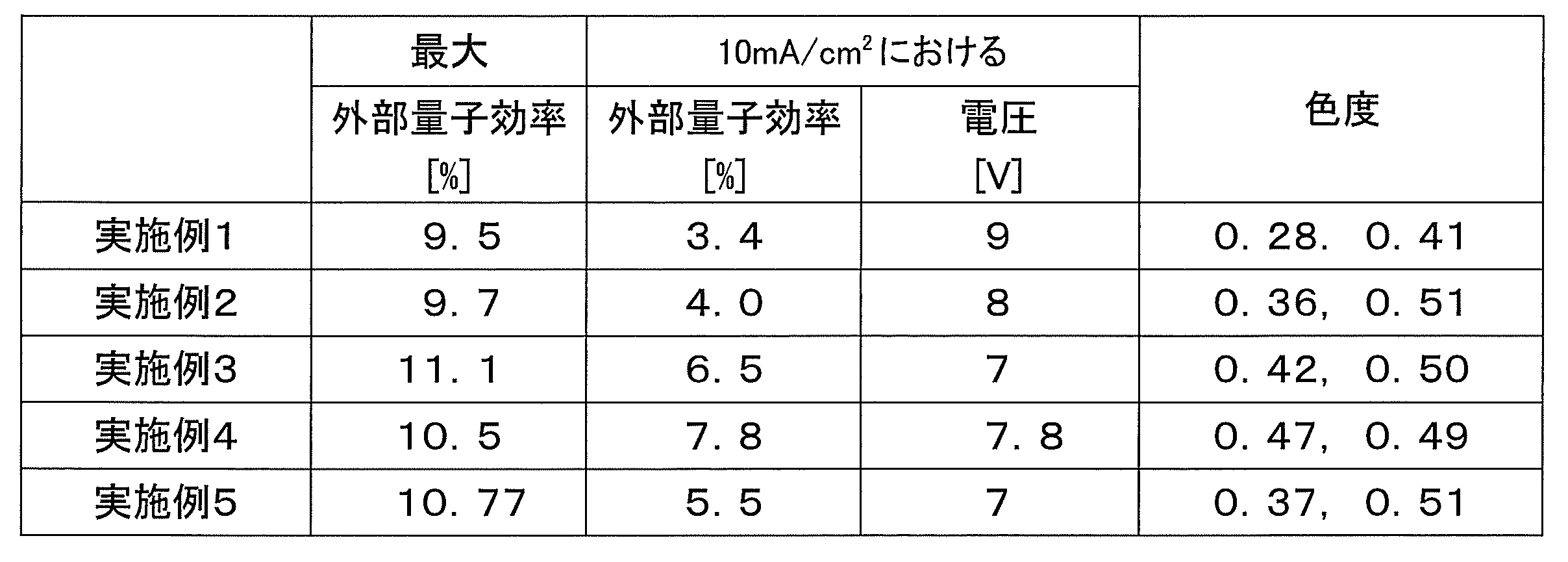
本実施例において、青色発光材料、緑色発光材料、赤色発光材料のすべてが遅延蛍光材料である多波長発光型の有機エレクトロルミネッセンス素子を作製して評価した。
膜厚100nmのインジウム・スズ酸化物(ITO)からなる陽極が形成されたガラス基板上に、各薄膜を真空蒸着法にて、真空度5.0×10⁻⁴Paで積層した。まず、ITO上にHATCNを10nmの厚さに形成し、TrisPCzを35nmの厚さに形成した。次いで、緑色発光材料であるPXZ-TRZとmCBPを異なる蒸着源から共蒸着し、6nmの厚さの層を形成して第1発光層とした(TXZ-TRZの濃度は10重量%)。次に、TXZ-TRZと赤色発光材料である4CzTPN-PhとmCBPを異なる蒸着源から共蒸着し、3nmの厚さの層を形成して第2発光層とした(TXZ-TRZの濃度は6重量%、4CzTPN-Phの濃度は2重量%)。さらに、青色発光材料であるSHT02とDPEPOを異なる蒸着源から共蒸着し、6nmの厚さの層を形成して第3発光層とした(SHT02の濃度は6重量%)。次いで、DPEPOを10nmの厚さに形成し、TmPyPbを40nmの厚さに形成した。さらにフッ化リチウム(LiF)を0.8nm真空蒸着し、次いでアルミニウム(Al)を100nmの厚さに蒸着することにより陰極を形成し、有機エレクトロルミネッセンス素子Aとした(実施例6)。
10nm厚のDPEPO層のかわりに10nm厚のPPT層を形成した点を変更して、有機エレクトロルミネッセンス素子Aと同様の製法により有機エレクトロルミネッセンス素子Bを作製した(実施例7)。
また、10nm厚のDPEPO層を形成しなかった点を変更して、有機エレクトロルミネッセンス素子Aと同様の製法により有機エレクトロルミネッセンス素子Cを作製した(実施例8)。
作製した有機エレクトロルミネッセンス素子Aの発光スペクトルを図17に示す。色度は0.31,0.36であった。また、作製した有機エレクトロルミネッセンス素子A~Cの電圧-電流密度特性を図18に示し、電流密度-外部量子効率特性を図19に示し、エネルギーバンド図を図20に示す。有機エレクトロルミネッセンス素子A~Cは白色発光素子として良好な発光特性を示し、有機エレクトロルミネッセンス素子Aは外部量子効率11.8%を達成した。
本実施例において、別の緑色発光材料を用いて、青色発光材料、緑色発光材料、赤色発光材料のすべてが遅延蛍光材料である多波長発光型の有機エレクトロルミネッセンス素子を作製して評価した。
緑色発光材料としてPXZ-TRZのかわりに4CzPNを用いて、第1発光層、第2発光層、第3発光層の厚さを下記のように変更して、実施例6の有機エレクトロルミネッセンス素子Aと同様の製法により有機エレクトロルミネッセンス素子D~Fを作製した。
素子D:第1発光層(6nm)、第2発光層(3nm)、第3発光層(6nm)
素子E:第1発光層(4nm)、第2発光層(3nm)、第3発光層(8nm)
素子F:第1発光層(3nm)、第2発光層(2nm)、第3発光層(15nm)
作製した有機エレクトロルミネッセンス素子D~Fの発光スペクトルを図21に示す。有機エレクトロルミネッセンス素子Fの色度は0.30,0.39であった。また、作製した有機エレクトロルミネッセンス素子D~Fの電圧-電流密度特性を図22に示し、電流密度-外部量子効率特性を図23に示す。有機エレクトロルミネッセンス素子Fは白色発光素子として良好な発光特性を示し、外部量子効率12.1%を達成した。
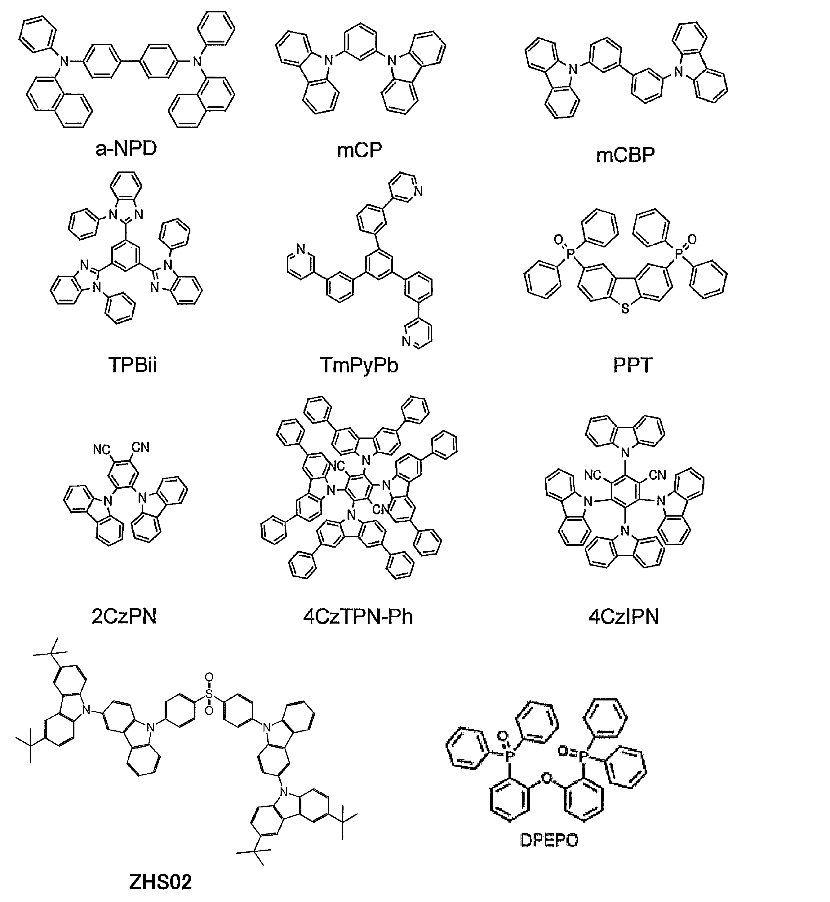

2 陽極
3 正孔注入層
4 正孔輸送層
5 発光層
6 電子輸送層
7 電子注入層
8 陰極
Claims (18)
- 陰極、陽極、および複数の発光材料を含む少なくとも1層の有機層を前記陰極と前記陽極の間に有しており、前記複数の発光材料から発光する多波長発光型の有機エレクトロルミネッセンス素子であり、前記発光材料からの発光のうちで最も短波長な発光が遅延蛍光を含む有機エレクトロルミネッセンス素子。
- 最も短波長で発光する発光材料が、他の発光材料のホスト材料を兼ねているか、あるいは、単独で有機層を形成していることを特徴とする請求項1に記載の有機エレクトロルミネッセンス素子。
- 最も短波長で発光する発光材料における、5Kの最低励起三重項エネルギー準位と最低励起一重項エネルギー準位のエネルギー差(ΔEST)が0.3eV以下であることを特徴とする請求項1または2に記載の有機エレクトロルミネッセンス素子。
- 最も短波長で発光する発光材料が青色発光材料であることを特徴とする請求項1~3のいずれか1項に記載の有機エレクトロルミネッセンス素子。
- 最も短波長で発光する発光材料の発光強度が全発光の20%超であることを特徴とする請求項1~4のいずれか1項に記載の有機エレクトロルミネッセンス素子。
- 最も短波長で発光する発光材料とそれ以外の波長で発光する少なくとも1種の発光材料が1つの有機層に含まれており、前記最も短波長で発光する発光材料がホスト材料としても機能することを特徴とする請求項1~5のいずれか1項に記載の有機エレクトロルミネッセンス素子。
- 最も短波長で発光する発光材料とそれ以外の波長で発光する少なくとも2種の発光材料が1つの有機層に含まれており、前記最も短波長で発光する発光材料が発光材料がホスト材料としても機能することを特徴とする請求項1~5のいずれか1項に記載の有機エレクトロルミネッセンス素子。
- 最も短波長で発光する発光材料が、単独で少なくとも1層の有機層を形成していることを特徴とする請求項1~7のいずれか1項に記載の有機エレクトロルミネッセンス素子。
- 発光材料を含む層が2層以上形成されており、そのうち陰極に最も近い層と陽極に最も近い層がともに最も短波長で発光する発光材料を含む層であることを特徴とする請求項1~8のいずれか1項に記載の有機エレクトロルミネッセンス素子。
- 前記陰極に最も近い層と前記陽極に最も近い層の間に、最も短波長で発光する発光材料をホスト材料として含む層を有することを特徴とする請求項9に記載の有機エレクトロルミネッセンス素子。
- 青色発光材料に緑色発光材料または赤色発光材料をドープした層を含むことを特徴とする請求項1~10のいずれか1項に記載の有機エレクトロルミネッセンス素子。
- 青色発光材料を含む層と青色発光材料に緑色発光材料または赤色発光材料をドープした層と青色発光材料を含む層を積層した層を含むことを特徴とする請求項1~10のいずれか1項に記載の有機エレクトロルミネッセンス素子。
- 前記複数の発光材料が、青色発光材料、緑色発光材料および赤色発光材料を含むことを特徴とする請求項1~12のいずれか1項に記載の有機エレクトロルミネッセンス素子。
- 青色発光材料に緑色発光材料と赤色発光材料をドープした層を含むことを特徴とする請求項1~13のいずれか1項に記載の有機エレクトロルミネッセンス素子。
- 緑色発光材料を含む層と緑色発光材料に赤色発光材料をドープした層と青色発光材料を含む層を積層した構造を含むことを特徴とする請求項1~14のいずれか1項に記載の有機エレクトロルミネッセンス素子。
- 前記複数の発光材料のすべてが遅延蛍光を発することを特徴とする請求項1~15のいずれか1項に記載の有機エレクトロルミネッセンス素子。
- 前記複数の発光材料のうちの少なくとも1つがリン光を発光することを特徴とする請求項1~15のいずれか1項に記載の有機エレクトロルミネッセンス素子。
- 前記複数の発光材料からの発光が混色して白色発光することを特徴とする請求項1~17のいずれか1項に記載の有機エレクトロルミネッセンス素子。
Priority Applications (6)
| Application Number | Priority Date | Filing Date | Title |
|---|---|---|---|
| EP14773887.6A EP2980877B1 (en) | 2013-03-29 | 2014-03-28 | Organic electroluminescent element |
| KR1020157030984A KR102144606B1 (ko) | 2013-03-29 | 2014-03-28 | 유기 일렉트로 루미네선스 소자 |
| ES14773887.6T ES2661409T3 (es) | 2013-03-29 | 2014-03-28 | Dispositivo electroluminiscente orgánico |
| JP2015508759A JP6513565B2 (ja) | 2013-03-29 | 2014-03-28 | 有機エレクトロルミネッセンス素子 |
| US14/781,083 US10600983B2 (en) | 2013-03-29 | 2014-03-28 | Organic electroluminescent device comprising delayed fluorescent materials |
| CN201480019195.2A CN105074951B (zh) | 2013-03-29 | 2014-03-28 | 有机电致发光元件 |
Applications Claiming Priority (2)
| Application Number | Priority Date | Filing Date | Title |
|---|---|---|---|
| JP2013074419 | 2013-03-29 | ||
| JP2013-074419 | 2013-03-29 |
Publications (1)
| Publication Number | Publication Date |
|---|---|
| WO2014157619A1 true WO2014157619A1 (ja) | 2014-10-02 |
Family
ID=51624575
Family Applications (1)
| Application Number | Title | Priority Date | Filing Date |
|---|---|---|---|
| PCT/JP2014/059121 Ceased WO2014157619A1 (ja) | 2013-03-29 | 2014-03-28 | 有機エレクトロルミネッセンス素子 |
Country Status (8)
| Country | Link |
|---|---|
| US (1) | US10600983B2 (ja) |
| EP (1) | EP2980877B1 (ja) |
| JP (1) | JP6513565B2 (ja) |
| KR (1) | KR102144606B1 (ja) |
| CN (1) | CN105074951B (ja) |
| ES (1) | ES2661409T3 (ja) |
| TW (1) | TWI661589B (ja) |
| WO (1) | WO2014157619A1 (ja) |
Cited By (33)
| Publication number | Priority date | Publication date | Assignee | Title |
|---|---|---|---|---|
| JP2015053476A (ja) * | 2013-07-30 | 2015-03-19 | 出光興産株式会社 | 有機エレクトロルミネッセンス素子および電子機器 |
| WO2015072470A1 (ja) * | 2013-11-12 | 2015-05-21 | 国立大学法人九州大学 | 発光材料、並びに、これを用いた遅延蛍光体および有機発光素子 |
| JP2015179817A (ja) * | 2013-08-14 | 2015-10-08 | 国立大学法人九州大学 | 有機エレクトロルミネッセンス素子 |
| WO2016017757A1 (ja) * | 2014-07-31 | 2016-02-04 | コニカミノルタ株式会社 | 有機エレクトロルミネッセンス素子、表示装置、照明装置、π共役系化合物、発光性薄膜 |
| WO2016017684A1 (ja) * | 2014-07-31 | 2016-02-04 | コニカミノルタ株式会社 | 有機エレクトロルミネッセンス素子材料、有機エレクトロルミネッセンス素子、発光性薄膜、表示装置及び照明装置 |
| WO2016068277A1 (ja) * | 2014-10-31 | 2016-05-06 | 国立大学法人九州大学 | 有機発光素子 |
| JP2016092280A (ja) * | 2014-11-07 | 2016-05-23 | コニカミノルタ株式会社 | 発光性薄膜、有機エレクトロルミネッセンス素子、照明装置及び表示装置 |
| JP2016119355A (ja) * | 2014-12-19 | 2016-06-30 | コニカミノルタ株式会社 | 有機エレクトロルミネッセンス素子 |
| WO2016125807A1 (ja) * | 2015-02-06 | 2016-08-11 | 出光興産株式会社 | 有機エレクトロルミネッセンス素子および電子機器 |
| WO2016129536A1 (ja) * | 2015-02-13 | 2016-08-18 | 出光興産株式会社 | 有機el発光装置および電子機器 |
| WO2016140180A1 (ja) * | 2015-03-02 | 2016-09-09 | Lumiotec株式会社 | 有機エレクトロルミネッセント素子及び照明装置 |
| JP2016167441A (ja) * | 2015-03-02 | 2016-09-15 | Lumiotec株式会社 | 有機エレクトロルミネッセント素子及び照明装置 |
| WO2016152605A1 (ja) * | 2015-03-23 | 2016-09-29 | 保土谷化学工業株式会社 | 有機エレクトロルミネッセンス素子用材料、発光材料および有機エレクトロルミネッセンス素子 |
| DE102015106941A1 (de) * | 2015-05-05 | 2016-11-10 | Osram Oled Gmbh | Organische Emitterschicht, organische Leuchtdiode und Verwendung von Schweratomen in einer organischen Emitterschicht einer organischen Leuchtdiode |
| JP2017503343A (ja) * | 2013-12-17 | 2017-01-26 | 北京維信諾科技有限公司 | 有機エレクトロルミネッセン素子及びその製造方法 |
| JP2017054972A (ja) * | 2015-09-10 | 2017-03-16 | コニカミノルタ株式会社 | 有機エレクトロルミネッセンス素子、表示装置、照明装置、π共役系化合物、及び発光性薄膜 |
| JP2017108100A (ja) * | 2015-08-07 | 2017-06-15 | 株式会社半導体エネルギー研究所 | 発光素子、表示装置、電子機器、及び照明装置 |
| WO2017115068A1 (en) * | 2015-12-29 | 2017-07-06 | University Court Of The University Of St Andrews | Light emitting compounds |
| JP2017126598A (ja) * | 2016-01-12 | 2017-07-20 | 凸版印刷株式会社 | 有機エレクトロルミネッセンス素子 |
| JP2017206666A (ja) * | 2016-05-23 | 2017-11-24 | コニカミノルタ株式会社 | 発光性分子集合体とその発光方法 |
| WO2018030446A1 (ja) * | 2016-08-10 | 2018-02-15 | 出光興産株式会社 | 有機エレクトロルミネッセンス素子、及び電子機器 |
| JP2018111751A (ja) * | 2017-01-10 | 2018-07-19 | 国立大学法人九州大学 | 発光材料、化合物および有機発光素子 |
| WO2019009307A1 (ja) * | 2017-07-03 | 2019-01-10 | 三菱ケミカル株式会社 | Oled素子形成用組成物及びoled素子 |
| JP2019501527A (ja) * | 2015-12-15 | 2019-01-17 | クンシャン ニュー フラット パネル ディスプレイ テクノロジー センター カンパニー リミテッド | 有機発光表示デバイス及び表示装置 |
| WO2020111205A1 (ja) * | 2018-11-30 | 2020-06-04 | 株式会社Kyulux | 有機発光素子 |
| US10693096B2 (en) | 2016-03-18 | 2020-06-23 | Sharp Kabushiki Kaisha | EL element and method for manufacturing EL element with a light-emitting layer including an ionic liquid, a phosphorescent material, and a fluorescent material |
| JP2020520103A (ja) * | 2017-05-08 | 2020-07-02 | サイノラ ゲゼルシャフト ミット ベシュレンクテル ハフツング | 青色光を発光する有機エレクトロルミネセントデバイス |
| JP2020520104A (ja) * | 2017-05-08 | 2020-07-02 | サイノラ ゲゼルシャフト ミット ベシュレンクテル ハフツング | 青色光を発光する有機エレクトロルミネセントデバイス |
| JP2020105341A (ja) * | 2018-12-27 | 2020-07-09 | 日鉄ケミカル&マテリアル株式会社 | 熱活性化遅延蛍光発光材料、及び有機電界発光素子 |
| JPWO2020111277A1 (ja) * | 2018-11-30 | 2021-10-14 | 株式会社Kyulux | 膜の製造方法、有機半導体素子の製造方法および有機半導体素子 |
| JP2021166196A (ja) * | 2015-02-24 | 2021-10-14 | 株式会社半導体エネルギー研究所 | 発光素子、発光装置、電子機器、及び照明装置 |
| WO2021241677A1 (ja) * | 2020-05-29 | 2021-12-02 | 株式会社Kyulux | 有機発光素子 |
| WO2022107798A1 (ja) * | 2020-11-17 | 2022-05-27 | 株式会社Kyulux | 有機エレクトロルミネッセンス素子、発光組成物の設計方法およびプログラム |
Families Citing this family (14)
| Publication number | Priority date | Publication date | Assignee | Title |
|---|---|---|---|---|
| JP5905916B2 (ja) * | 2013-12-26 | 2016-04-20 | 出光興産株式会社 | 有機エレクトロルミネッセンス素子および電子機器 |
| EP3117470B1 (de) * | 2014-03-13 | 2020-12-23 | Merck Patent GmbH | Organische elektrolumineszenzvorrichtung |
| WO2018047853A1 (ja) * | 2016-09-06 | 2018-03-15 | 株式会社Kyulux | 有機発光素子 |
| CN106410053B (zh) * | 2016-10-31 | 2019-01-18 | 昆山工研院新型平板显示技术中心有限公司 | 一种白光有机电致发光器件 |
| CN106972111B (zh) * | 2017-06-01 | 2018-11-20 | 上海天马有机发光显示技术有限公司 | 有机发光器件和显示装置 |
| CN107256927B (zh) * | 2017-06-13 | 2020-01-24 | 上海天马有机发光显示技术有限公司 | 有机发光器件和显示装置 |
| CN107507921B (zh) * | 2017-09-29 | 2019-05-14 | 江苏三月光电科技有限公司 | 一种含硼有机电致发光器件及其制备方法 |
| EP3696167B1 (en) | 2018-07-27 | 2024-11-20 | Idemitsu Kosan Co.,Ltd. | Compound, material for organic electroluminescence element, organic electroluminescence element, and electronic device |
| KR102743332B1 (ko) * | 2018-12-19 | 2024-12-18 | 삼성디스플레이 주식회사 | 유기 발광 소자 및 이를 포함하는 표시 장치 |
| KR102698882B1 (ko) | 2019-05-31 | 2024-08-28 | 삼성디스플레이 주식회사 | 유기 발광 소자 및 전자 장치 |
| KR102943183B1 (ko) * | 2019-11-29 | 2026-03-23 | 삼성전자주식회사 | 유기 발광 소자 |
| KR102919367B1 (ko) * | 2020-09-18 | 2026-01-28 | 삼성디스플레이 주식회사 | 유기 전계 발광 소자 |
| JP7838780B2 (ja) * | 2021-05-20 | 2026-04-01 | 株式会社Kyulux | 有機発光素子 |
| US20240260452A1 (en) * | 2022-12-30 | 2024-08-01 | ND-Materials Corp. | Light-emitting down conversion organic nano-dot, composition for color conversion film comprising thereof, and conversion film, display device and light emitting diode device prepared therefrom |
Citations (16)
| Publication number | Priority date | Publication date | Assignee | Title |
|---|---|---|---|---|
| JP2010114070A (ja) | 2008-10-10 | 2010-05-20 | Canon Inc | 白色有機el素子 |
| US20120097998A1 (en) * | 2010-10-26 | 2012-04-26 | Sung-Hoon Pieh | White Organic Light Emitting Device |
| JP2012089513A (ja) | 2005-03-15 | 2012-05-10 | Novaled Ag | 発光素子 |
| WO2012064987A1 (en) * | 2010-11-11 | 2012-05-18 | Nitto Denko Corporation | Hybrid composite emissive construct and light-emitting devices using the same |
| WO2012133188A1 (ja) * | 2011-03-25 | 2012-10-04 | 出光興産株式会社 | 有機エレクトロルミネッセンス素子 |
| WO2013011955A1 (ja) | 2011-07-15 | 2013-01-24 | 国立大学法人九州大学 | 遅延蛍光材料およびそれを用いた有機エレクトロルミネッセンス素子 |
| WO2013011954A1 (ja) | 2011-07-15 | 2013-01-24 | 国立大学法人九州大学 | 有機エレクトロルミネッセンス素子およびそれに用いる化合物 |
| WO2013081088A1 (ja) | 2011-12-02 | 2013-06-06 | 国立大学法人九州大学 | 有機発光素子ならびにそれに用いる遅延蛍光材料および化合物 |
| JP2013116975A (ja) | 2011-12-02 | 2013-06-13 | Kyushu Univ | 遅延蛍光材料、有機発光素子および化合物 |
| WO2013133359A1 (ja) | 2012-03-09 | 2013-09-12 | 国立大学法人九州大学 | 発光材料および有機発光素子 |
| WO2013154064A1 (ja) | 2012-04-09 | 2013-10-17 | 国立大学法人九州大学 | 有機発光素子ならびにそれに用いる発光材料および化合物 |
| WO2013161437A1 (ja) | 2012-04-25 | 2013-10-31 | 国立大学法人九州大学 | 発光材料および有機発光素子 |
| JP2013256490A (ja) | 2012-05-17 | 2013-12-26 | Kyushu Univ | 化合物、発光材料および有機発光素子 |
| JP2014009224A (ja) | 2012-07-03 | 2014-01-20 | Kyushu Univ | 発光材料、化合物および有機発光素子 |
| JP2014009352A (ja) | 2012-07-03 | 2014-01-20 | Kyushu Univ | 発光材料、化合物および有機発光素子 |
| JP2014075249A (ja) * | 2012-10-03 | 2014-04-24 | Idemitsu Kosan Co Ltd | 有機エレクトロルミネッセンス素子 |
Family Cites Families (14)
| Publication number | Priority date | Publication date | Assignee | Title |
|---|---|---|---|---|
| KR0133352Y1 (ko) | 1996-02-12 | 1999-03-30 | 김광호 | 정착기 과열 방지회로 |
| JP4024009B2 (ja) | 2000-04-21 | 2007-12-19 | Tdk株式会社 | 有機el素子 |
| KR100841363B1 (ko) | 2006-11-22 | 2008-06-26 | 삼성에스디아이 주식회사 | 유기전계발광표시장치 및 그의 제조방법 |
| JP2010114428A (ja) * | 2008-10-10 | 2010-05-20 | Canon Inc | 有機el表示装置 |
| JP5448680B2 (ja) * | 2008-10-10 | 2014-03-19 | キヤノン株式会社 | 表示装置 |
| US20100295444A1 (en) | 2009-05-22 | 2010-11-25 | Idemitsu Kosan Co., Ltd. | Organic electroluminescence device |
| JP5573416B2 (ja) | 2010-06-29 | 2014-08-20 | 東洋インキScホールディングス株式会社 | カラーフィルタおよびカラー表示装置 |
| KR20100133352A (ko) * | 2010-12-06 | 2010-12-21 | 제일모직주식회사 | 유기 광전 소자 |
| JP6158543B2 (ja) * | 2012-04-13 | 2017-07-05 | 株式会社半導体エネルギー研究所 | 発光素子、発光装置、電子機器、および照明装置 |
| JP6158542B2 (ja) * | 2012-04-13 | 2017-07-05 | 株式会社半導体エネルギー研究所 | 発光素子、発光装置、電子機器、および照明装置 |
| JP5925308B2 (ja) | 2012-06-01 | 2016-05-25 | 出光興産株式会社 | 有機エレクトロルミネッセンス素子 |
| TWI650399B (zh) * | 2012-08-03 | 2019-02-11 | 日商半導體能源研究所股份有限公司 | 發光元件 |
| KR102058262B1 (ko) * | 2012-09-03 | 2019-12-20 | 호도가야 가가쿠 고교 가부시키가이샤 | 인데노 아크리단 환 구조를 가지는 화합물 및 유기 일렉트로루미네선스 소자 |
| MX2020009142A (es) | 2018-03-12 | 2021-01-08 | Omega Energy Sistems Llc | Recolector de energía de estado sólido de suboxidos de metales de transición. |
-
2014
- 2014-03-28 TW TW103111858A patent/TWI661589B/zh active
- 2014-03-28 EP EP14773887.6A patent/EP2980877B1/en active Active
- 2014-03-28 KR KR1020157030984A patent/KR102144606B1/ko active Active
- 2014-03-28 WO PCT/JP2014/059121 patent/WO2014157619A1/ja not_active Ceased
- 2014-03-28 CN CN201480019195.2A patent/CN105074951B/zh active Active
- 2014-03-28 JP JP2015508759A patent/JP6513565B2/ja active Active
- 2014-03-28 US US14/781,083 patent/US10600983B2/en active Active
- 2014-03-28 ES ES14773887.6T patent/ES2661409T3/es active Active
Patent Citations (16)
| Publication number | Priority date | Publication date | Assignee | Title |
|---|---|---|---|---|
| JP2012089513A (ja) | 2005-03-15 | 2012-05-10 | Novaled Ag | 発光素子 |
| JP2010114070A (ja) | 2008-10-10 | 2010-05-20 | Canon Inc | 白色有機el素子 |
| US20120097998A1 (en) * | 2010-10-26 | 2012-04-26 | Sung-Hoon Pieh | White Organic Light Emitting Device |
| WO2012064987A1 (en) * | 2010-11-11 | 2012-05-18 | Nitto Denko Corporation | Hybrid composite emissive construct and light-emitting devices using the same |
| WO2012133188A1 (ja) * | 2011-03-25 | 2012-10-04 | 出光興産株式会社 | 有機エレクトロルミネッセンス素子 |
| WO2013011955A1 (ja) | 2011-07-15 | 2013-01-24 | 国立大学法人九州大学 | 遅延蛍光材料およびそれを用いた有機エレクトロルミネッセンス素子 |
| WO2013011954A1 (ja) | 2011-07-15 | 2013-01-24 | 国立大学法人九州大学 | 有機エレクトロルミネッセンス素子およびそれに用いる化合物 |
| JP2013116975A (ja) | 2011-12-02 | 2013-06-13 | Kyushu Univ | 遅延蛍光材料、有機発光素子および化合物 |
| WO2013081088A1 (ja) | 2011-12-02 | 2013-06-06 | 国立大学法人九州大学 | 有機発光素子ならびにそれに用いる遅延蛍光材料および化合物 |
| WO2013133359A1 (ja) | 2012-03-09 | 2013-09-12 | 国立大学法人九州大学 | 発光材料および有機発光素子 |
| WO2013154064A1 (ja) | 2012-04-09 | 2013-10-17 | 国立大学法人九州大学 | 有機発光素子ならびにそれに用いる発光材料および化合物 |
| WO2013161437A1 (ja) | 2012-04-25 | 2013-10-31 | 国立大学法人九州大学 | 発光材料および有機発光素子 |
| JP2013256490A (ja) | 2012-05-17 | 2013-12-26 | Kyushu Univ | 化合物、発光材料および有機発光素子 |
| JP2014009224A (ja) | 2012-07-03 | 2014-01-20 | Kyushu Univ | 発光材料、化合物および有機発光素子 |
| JP2014009352A (ja) | 2012-07-03 | 2014-01-20 | Kyushu Univ | 発光材料、化合物および有機発光素子 |
| JP2014075249A (ja) * | 2012-10-03 | 2014-04-24 | Idemitsu Kosan Co Ltd | 有機エレクトロルミネッセンス素子 |
Non-Patent Citations (1)
| Title |
|---|
| See also references of EP2980877A4 |
Cited By (99)
| Publication number | Priority date | Publication date | Assignee | Title |
|---|---|---|---|---|
| JP2015053476A (ja) * | 2013-07-30 | 2015-03-19 | 出光興産株式会社 | 有機エレクトロルミネッセンス素子および電子機器 |
| US11944010B2 (en) | 2013-08-14 | 2024-03-26 | Kyulux, Inc. | Organic electroluminescent device |
| JP2015179817A (ja) * | 2013-08-14 | 2015-10-08 | 国立大学法人九州大学 | 有機エレクトロルミネッセンス素子 |
| JP2015179809A (ja) * | 2013-08-14 | 2015-10-08 | 国立大学法人九州大学 | 有機エレクトロルミネッセンス素子 |
| EP3035401A4 (en) * | 2013-08-14 | 2017-01-04 | Kyushu University, National University Corporation | Organic electroluminescent element |
| EP3035401A1 (en) | 2013-08-14 | 2016-06-22 | Kyushu University, National University Corporation | Organic electroluminescent element |
| EP4152910A1 (en) * | 2013-08-14 | 2023-03-22 | Kyulux, Inc. | Organic electroluminescent device |
| US10862047B2 (en) | 2013-08-14 | 2020-12-08 | Kyushu University, National University Corporation | Organic electroluminescent device |
| US11450817B2 (en) | 2013-08-14 | 2022-09-20 | Kyulux, Inc. | Organic electroluminescent device |
| US11101433B2 (en) | 2013-11-12 | 2021-08-24 | Kyulux, Inc. | Light-emitting material, and delayed fluorescent emitter and organic light-emitting device using same |
| WO2015072470A1 (ja) * | 2013-11-12 | 2015-05-21 | 国立大学法人九州大学 | 発光材料、並びに、これを用いた遅延蛍光体および有機発光素子 |
| JPWO2015072470A1 (ja) * | 2013-11-12 | 2017-03-16 | 株式会社Kyulux | 発光材料、並びに、これを用いた遅延蛍光体および有機発光素子 |
| US10312453B2 (en) | 2013-12-17 | 2019-06-04 | Beijing Visionox Technology Co., Ltd. | Organic electroluminescent device and method for manufacture thereof |
| JP2017503343A (ja) * | 2013-12-17 | 2017-01-26 | 北京維信諾科技有限公司 | 有機エレクトロルミネッセン素子及びその製造方法 |
| WO2016017757A1 (ja) * | 2014-07-31 | 2016-02-04 | コニカミノルタ株式会社 | 有機エレクトロルミネッセンス素子、表示装置、照明装置、π共役系化合物、発光性薄膜 |
| US10950799B2 (en) | 2014-07-31 | 2021-03-16 | Merck Patent Gmbh | Organic electroluminescent element, display device, lighting device, PI-conjugated compound, and light-emitting thin film |
| US11329234B2 (en) | 2014-07-31 | 2022-05-10 | Merck Patent Gmbh | Organic electroluminescent element, display device, lighting device, π-conjugated compound, and light-emitting thin film |
| WO2016017684A1 (ja) * | 2014-07-31 | 2016-02-04 | コニカミノルタ株式会社 | 有機エレクトロルミネッセンス素子材料、有機エレクトロルミネッセンス素子、発光性薄膜、表示装置及び照明装置 |
| JPWO2016017757A1 (ja) * | 2014-07-31 | 2017-05-25 | コニカミノルタ株式会社 | 有機エレクトロルミネッセンス素子、表示装置、照明装置、π共役系化合物、発光性薄膜 |
| JPWO2016017684A1 (ja) * | 2014-07-31 | 2017-05-18 | コニカミノルタ株式会社 | 有機エレクトロルミネッセンス素子材料、有機エレクトロルミネッセンス素子、発光性薄膜、表示装置及び照明装置 |
| TWI666802B (zh) * | 2014-10-31 | 2019-07-21 | Kyushu University, National University Corporation | 有機發光元件 |
| CN107112421B (zh) * | 2014-10-31 | 2019-01-11 | 国立大学法人九州大学 | 有机发光元件 |
| US20170309857A1 (en) | 2014-10-31 | 2017-10-26 | Kyushu University, National University Corporation | Organic light-emitting device |
| EP3214666A4 (en) * | 2014-10-31 | 2018-06-13 | Kyushu University National University Corporation | Organic light emitting element |
| KR20170077186A (ko) * | 2014-10-31 | 2017-07-05 | 고쿠리쓰다이가쿠호진 규슈다이가쿠 | 유기 발광 소자 |
| KR101994010B1 (ko) * | 2014-10-31 | 2019-06-27 | 고쿠리쓰다이가쿠호진 규슈다이가쿠 | 유기 발광 소자 |
| CN107112421A (zh) * | 2014-10-31 | 2017-08-29 | 国立大学法人九州大学 | 有机发光元件 |
| JP2016092134A (ja) * | 2014-10-31 | 2016-05-23 | 国立大学法人九州大学 | 有機発光素子 |
| WO2016068277A1 (ja) * | 2014-10-31 | 2016-05-06 | 国立大学法人九州大学 | 有機発光素子 |
| US10290824B2 (en) | 2014-10-31 | 2019-05-14 | Kyushu University, National University Corporation | Organic light-emitting device |
| JP2016092280A (ja) * | 2014-11-07 | 2016-05-23 | コニカミノルタ株式会社 | 発光性薄膜、有機エレクトロルミネッセンス素子、照明装置及び表示装置 |
| JP2016119355A (ja) * | 2014-12-19 | 2016-06-30 | コニカミノルタ株式会社 | 有機エレクトロルミネッセンス素子 |
| EP3255693B1 (en) * | 2015-02-06 | 2024-10-09 | Idemitsu Kosan Co., Ltd | Organic electroluminescence element and electronic device |
| JPWO2016125807A1 (ja) * | 2015-02-06 | 2017-11-24 | 出光興産株式会社 | 有機エレクトロルミネッセンス素子および電子機器 |
| KR102660767B1 (ko) * | 2015-02-06 | 2024-04-24 | 이데미쓰 고산 가부시키가이샤 | 유기 일렉트로루미네센스 소자 및 전자 기기 |
| KR20170110614A (ko) * | 2015-02-06 | 2017-10-11 | 이데미쓰 고산 가부시키가이샤 | 유기 일렉트로루미네센스 소자 및 전자 기기 |
| CN107112431A (zh) * | 2015-02-06 | 2017-08-29 | 出光兴产株式会社 | 有机电致发光元件和电子设备 |
| US10351765B2 (en) | 2015-02-06 | 2019-07-16 | Idemitsu Kosan Co., Ltd. | Organic electroluminescence element and electronic device |
| US10125310B2 (en) | 2015-02-06 | 2018-11-13 | Idemitsu Kosan Co., Ltd. | Organic electroluminescence element and electronic device |
| CN107112431B (zh) * | 2015-02-06 | 2019-08-23 | 出光兴产株式会社 | 有机电致发光元件和电子设备 |
| TWI726865B (zh) * | 2015-02-06 | 2021-05-11 | 日商出光興產股份有限公司 | 有機電致發光元件及電子機器 |
| WO2016125807A1 (ja) * | 2015-02-06 | 2016-08-11 | 出光興産株式会社 | 有機エレクトロルミネッセンス素子および電子機器 |
| KR102510747B1 (ko) * | 2015-02-13 | 2023-03-15 | 이데미쓰 고산 가부시키가이샤 | 유기 el 발광 장치 및 전자 기기 |
| CN107211503B (zh) * | 2015-02-13 | 2020-03-27 | 出光兴产株式会社 | 有机el发光装置和电子设备 |
| US11653511B2 (en) | 2015-02-13 | 2023-05-16 | Idemitsu Kosan Co., Ltd. | Organic EL light-emitting apparatus and electronic instrument |
| WO2016129536A1 (ja) * | 2015-02-13 | 2016-08-18 | 出光興産株式会社 | 有機el発光装置および電子機器 |
| JPWO2016129536A1 (ja) * | 2015-02-13 | 2017-12-07 | 出光興産株式会社 | 有機el発光装置および電子機器 |
| KR20170115498A (ko) * | 2015-02-13 | 2017-10-17 | 이데미쓰 고산 가부시키가이샤 | 유기 el 발광 장치 및 전자 기기 |
| CN107211503A (zh) * | 2015-02-13 | 2017-09-26 | 出光兴产株式会社 | 有机el发光装置和电子设备 |
| JP2021166196A (ja) * | 2015-02-24 | 2021-10-14 | 株式会社半導体エネルギー研究所 | 発光素子、発光装置、電子機器、及び照明装置 |
| US12089429B2 (en) | 2015-02-24 | 2024-09-10 | Semiconductor Energy Laboratory Co., Ltd. | Light-emitting element, light-emitting device, electronic device, and lighting device |
| JP2024091941A (ja) * | 2015-02-24 | 2024-07-05 | 株式会社半導体エネルギー研究所 | 発光素子 |
| US10084146B2 (en) | 2015-03-02 | 2018-09-25 | Lumiotec Inc. | Organic electroluminescent element and lighting device |
| JP2016167441A (ja) * | 2015-03-02 | 2016-09-15 | Lumiotec株式会社 | 有機エレクトロルミネッセント素子及び照明装置 |
| WO2016140180A1 (ja) * | 2015-03-02 | 2016-09-09 | Lumiotec株式会社 | 有機エレクトロルミネッセント素子及び照明装置 |
| WO2016152605A1 (ja) * | 2015-03-23 | 2016-09-29 | 保土谷化学工業株式会社 | 有機エレクトロルミネッセンス素子用材料、発光材料および有機エレクトロルミネッセンス素子 |
| US11239439B2 (en) | 2015-03-23 | 2022-02-01 | Hodogaya Chemical Co., Ltd. | Material for organic electroluminescent device, light-emitting material, and organic electroluminescent device |
| JPWO2016152605A1 (ja) * | 2015-03-23 | 2018-01-18 | 保土谷化学工業株式会社 | 有機エレクトロルミネッセンス素子用材料、発光材料および有機エレクトロルミネッセンス素子 |
| DE102015106941A1 (de) * | 2015-05-05 | 2016-11-10 | Osram Oled Gmbh | Organische Emitterschicht, organische Leuchtdiode und Verwendung von Schweratomen in einer organischen Emitterschicht einer organischen Leuchtdiode |
| JP2017108100A (ja) * | 2015-08-07 | 2017-06-15 | 株式会社半導体エネルギー研究所 | 発光素子、表示装置、電子機器、及び照明装置 |
| US11770969B2 (en) | 2015-08-07 | 2023-09-26 | Semiconductor Energy Laboratory Co., Ltd. | Light-emitting element, display device, electronic device, and lighting device |
| CN111710788A (zh) * | 2015-08-07 | 2020-09-25 | 株式会社半导体能源研究所 | 发光元件、显示装置、电子设备及照明装置 |
| KR102647906B1 (ko) * | 2015-08-07 | 2024-03-13 | 가부시키가이샤 한도오따이 에네루기 켄큐쇼 | 발광 장치, 표시 장치, 전자 기기, 및 조명 장치 |
| CN111710788B (zh) * | 2015-08-07 | 2023-07-21 | 株式会社半导体能源研究所 | 发光元件、显示装置、电子设备及照明装置 |
| US11145827B2 (en) | 2015-08-07 | 2021-10-12 | Semiconductor Energy Laboratory Co., Ltd. | Light-emitting element, display device, electronic device, and lighting device |
| US12365835B2 (en) | 2015-08-07 | 2025-07-22 | Semiconductor Energy Laboratory Co., Ltd. | Light-emitting element, display device, electronic device, and lighting device |
| KR20180039086A (ko) * | 2015-08-07 | 2018-04-17 | 가부시키가이샤 한도오따이 에네루기 켄큐쇼 | 발광 장치, 표시 장치, 전자 기기, 및 조명 장치 |
| JP2017054972A (ja) * | 2015-09-10 | 2017-03-16 | コニカミノルタ株式会社 | 有機エレクトロルミネッセンス素子、表示装置、照明装置、π共役系化合物、及び発光性薄膜 |
| JP2019501527A (ja) * | 2015-12-15 | 2019-01-17 | クンシャン ニュー フラット パネル ディスプレイ テクノロジー センター カンパニー リミテッド | 有機発光表示デバイス及び表示装置 |
| JP2019509977A (ja) * | 2015-12-29 | 2019-04-11 | ユニヴァーシティー コート オブ ザ ユニヴァーシティー オブ セント アンドリューズ | 発光性化合物 |
| WO2017115068A1 (en) * | 2015-12-29 | 2017-07-06 | University Court Of The University Of St Andrews | Light emitting compounds |
| JP2017126598A (ja) * | 2016-01-12 | 2017-07-20 | 凸版印刷株式会社 | 有機エレクトロルミネッセンス素子 |
| US10693096B2 (en) | 2016-03-18 | 2020-06-23 | Sharp Kabushiki Kaisha | EL element and method for manufacturing EL element with a light-emitting layer including an ionic liquid, a phosphorescent material, and a fluorescent material |
| JP2017206666A (ja) * | 2016-05-23 | 2017-11-24 | コニカミノルタ株式会社 | 発光性分子集合体とその発光方法 |
| WO2018030446A1 (ja) * | 2016-08-10 | 2018-02-15 | 出光興産株式会社 | 有機エレクトロルミネッセンス素子、及び電子機器 |
| US11189803B2 (en) | 2016-08-10 | 2021-11-30 | Idemitsu Kosan Co., Ltd. | Organic electroluminescent element and electronic device containing the organic electroluminescent element |
| JP2018111751A (ja) * | 2017-01-10 | 2018-07-19 | 国立大学法人九州大学 | 発光材料、化合物および有機発光素子 |
| JP7058288B2 (ja) | 2017-05-08 | 2022-04-21 | サイノラ ゲゼルシャフト ミット ベシュレンクテル ハフツング | 青色光を発光する有機エレクトロルミネセントデバイス |
| JP7058287B2 (ja) | 2017-05-08 | 2022-04-21 | サイノラ ゲゼルシャフト ミット ベシュレンクテル ハフツング | 青色光を発光する有機エレクトロルミネセントデバイス |
| JP2020520103A (ja) * | 2017-05-08 | 2020-07-02 | サイノラ ゲゼルシャフト ミット ベシュレンクテル ハフツング | 青色光を発光する有機エレクトロルミネセントデバイス |
| JP2020520104A (ja) * | 2017-05-08 | 2020-07-02 | サイノラ ゲゼルシャフト ミット ベシュレンクテル ハフツング | 青色光を発光する有機エレクトロルミネセントデバイス |
| JPWO2019009307A1 (ja) * | 2017-07-03 | 2020-06-18 | 三菱ケミカル株式会社 | Oled素子形成用組成物及びoled素子 |
| WO2019009307A1 (ja) * | 2017-07-03 | 2019-01-10 | 三菱ケミカル株式会社 | Oled素子形成用組成物及びoled素子 |
| JP7418794B2 (ja) | 2018-11-30 | 2024-01-22 | 株式会社Kyulux | 有機発光素子 |
| WO2020111205A1 (ja) * | 2018-11-30 | 2020-06-04 | 株式会社Kyulux | 有機発光素子 |
| JPWO2020111277A1 (ja) * | 2018-11-30 | 2021-10-14 | 株式会社Kyulux | 膜の製造方法、有機半導体素子の製造方法および有機半導体素子 |
| JP7393799B2 (ja) | 2018-11-30 | 2023-12-07 | 株式会社Kyulux | 膜の製造方法 |
| US12356787B2 (en) * | 2018-11-30 | 2025-07-08 | Kyulux, Inc. | Organic light emitting element |
| JP2020096178A (ja) * | 2018-11-30 | 2020-06-18 | 株式会社Kyulux | 有機発光素子 |
| US20220123249A1 (en) * | 2018-11-30 | 2022-04-21 | Kyulux, Inc. | Organic light emitting element |
| JP2024041803A (ja) * | 2018-11-30 | 2024-03-27 | 株式会社Kyulux | 有機発光素子 |
| JP2020105341A (ja) * | 2018-12-27 | 2020-07-09 | 日鉄ケミカル&マテリアル株式会社 | 熱活性化遅延蛍光発光材料、及び有機電界発光素子 |
| JP7094215B2 (ja) | 2018-12-27 | 2022-07-01 | 日鉄ケミカル&マテリアル株式会社 | 熱活性化遅延蛍光発光材料、及び有機電界発光素子 |
| JPWO2021241677A1 (ja) * | 2020-05-29 | 2021-12-02 | ||
| WO2021241677A1 (ja) * | 2020-05-29 | 2021-12-02 | 株式会社Kyulux | 有機発光素子 |
| JP7728589B2 (ja) | 2020-05-29 | 2025-08-25 | 株式会社Kyulux | 有機発光素子 |
| WO2022107798A1 (ja) * | 2020-11-17 | 2022-05-27 | 株式会社Kyulux | 有機エレクトロルミネッセンス素子、発光組成物の設計方法およびプログラム |
| JPWO2022107798A1 (ja) * | 2020-11-17 | 2022-05-27 | ||
| JP7840571B2 (ja) | 2020-11-17 | 2026-04-06 | 株式会社Kyulux | 有機エレクトロルミネッセンス素子、発光組成物の設計方法およびプログラム |
Also Published As
| Publication number | Publication date |
|---|---|
| US20160329512A1 (en) | 2016-11-10 |
| TW201503445A (zh) | 2015-01-16 |
| ES2661409T3 (es) | 2018-03-28 |
| EP2980877A1 (en) | 2016-02-03 |
| TWI661589B (zh) | 2019-06-01 |
| JPWO2014157619A1 (ja) | 2017-02-16 |
| KR102144606B1 (ko) | 2020-08-13 |
| KR20150135511A (ko) | 2015-12-02 |
| JP6513565B2 (ja) | 2019-05-22 |
| US10600983B2 (en) | 2020-03-24 |
| EP2980877B1 (en) | 2017-11-29 |
| CN105074951B (zh) | 2017-09-22 |
| EP2980877A4 (en) | 2016-10-26 |
| CN105074951A (zh) | 2015-11-18 |
Similar Documents
| Publication | Publication Date | Title |
|---|---|---|
| JP6513565B2 (ja) | 有機エレクトロルミネッセンス素子 | |
| JP5669163B1 (ja) | 有機エレクトロルミネッセンス素子 | |
| KR102196821B1 (ko) | 유기 발광 소자 | |
| JP6095643B2 (ja) | 発光材料および有機発光素子 | |
| JP7182774B2 (ja) | 発光素子 | |
| JP6494079B2 (ja) | 有機発光素子 | |
| JP6567504B2 (ja) | 有機発光素子 | |
| WO2017115833A1 (ja) | 有機エレクトロルミネッセンス素子 | |
| JP2016130231A (ja) | 化合物、混合物、発光層、有機発光素子およびアシストドーパント | |
| WO2016111196A1 (ja) | 化合物、混合物、発光層、有機発光素子およびアシストドーパント | |
| JP7337369B2 (ja) | 有機発光素子、積層体および発光方法 |
Legal Events
| Date | Code | Title | Description |
|---|---|---|---|
| WWE | Wipo information: entry into national phase |
Ref document number: 201480019195.2 Country of ref document: CN |
|
| 121 | Ep: the epo has been informed by wipo that ep was designated in this application |
Ref document number: 14773887 Country of ref document: EP Kind code of ref document: A1 |
|
| ENP | Entry into the national phase |
Ref document number: 2015508759 Country of ref document: JP Kind code of ref document: A |
|
| NENP | Non-entry into the national phase |
Ref country code: DE |
|
| WWE | Wipo information: entry into national phase |
Ref document number: 14781083 Country of ref document: US |
|
| ENP | Entry into the national phase |
Ref document number: 20157030984 Country of ref document: KR Kind code of ref document: A |
|
| REEP | Request for entry into the european phase |
Ref document number: 2014773887 Country of ref document: EP |
|
| WWE | Wipo information: entry into national phase |
Ref document number: 2014773887 Country of ref document: EP |