WO2014163056A1 - β-Ga2O3系単結晶の成長方法 - Google Patents
β-Ga2O3系単結晶の成長方法 Download PDFInfo
- Publication number
- WO2014163056A1 WO2014163056A1 PCT/JP2014/059572 JP2014059572W WO2014163056A1 WO 2014163056 A1 WO2014163056 A1 WO 2014163056A1 JP 2014059572 W JP2014059572 W JP 2014059572W WO 2014163056 A1 WO2014163056 A1 WO 2014163056A1
- Authority
- WO
- WIPO (PCT)
- Prior art keywords
- crystal
- single crystal
- substrate
- growing
- axis
- Prior art date
- Legal status (The legal status is an assumption and is not a legal conclusion. Google has not performed a legal analysis and makes no representation as to the accuracy of the status listed.)
- Ceased
Links
Images


Classifications
-
- C—CHEMISTRY; METALLURGY
- C30—CRYSTAL GROWTH
- C30B—SINGLE-CRYSTAL GROWTH; UNIDIRECTIONAL SOLIDIFICATION OF EUTECTIC MATERIAL OR UNIDIRECTIONAL DEMIXING OF EUTECTOID MATERIAL; REFINING BY ZONE-MELTING OF MATERIAL; PRODUCTION OF A HOMOGENEOUS POLYCRYSTALLINE MATERIAL WITH DEFINED STRUCTURE; SINGLE CRYSTALS OR HOMOGENEOUS POLYCRYSTALLINE MATERIAL WITH DEFINED STRUCTURE; AFTER-TREATMENT OF SINGLE CRYSTALS OR A HOMOGENEOUS POLYCRYSTALLINE MATERIAL WITH DEFINED STRUCTURE; APPARATUS THEREFOR
- C30B15/00—Single-crystal growth by pulling from a melt, e.g. Czochralski method
- C30B15/34—Edge-defined film-fed crystal-growth using dies or slits
-
- C—CHEMISTRY; METALLURGY
- C30—CRYSTAL GROWTH
- C30B—SINGLE-CRYSTAL GROWTH; UNIDIRECTIONAL SOLIDIFICATION OF EUTECTIC MATERIAL OR UNIDIRECTIONAL DEMIXING OF EUTECTOID MATERIAL; REFINING BY ZONE-MELTING OF MATERIAL; PRODUCTION OF A HOMOGENEOUS POLYCRYSTALLINE MATERIAL WITH DEFINED STRUCTURE; SINGLE CRYSTALS OR HOMOGENEOUS POLYCRYSTALLINE MATERIAL WITH DEFINED STRUCTURE; AFTER-TREATMENT OF SINGLE CRYSTALS OR A HOMOGENEOUS POLYCRYSTALLINE MATERIAL WITH DEFINED STRUCTURE; APPARATUS THEREFOR
- C30B15/00—Single-crystal growth by pulling from a melt, e.g. Czochralski method
- C30B15/02—Single-crystal growth by pulling from a melt, e.g. Czochralski method adding crystallising materials or reactants forming it in situ to the melt
- C30B15/04—Single-crystal growth by pulling from a melt, e.g. Czochralski method adding crystallising materials or reactants forming it in situ to the melt adding doping materials, e.g. for n-p-junction
-
- C—CHEMISTRY; METALLURGY
- C30—CRYSTAL GROWTH
- C30B—SINGLE-CRYSTAL GROWTH; UNIDIRECTIONAL SOLIDIFICATION OF EUTECTIC MATERIAL OR UNIDIRECTIONAL DEMIXING OF EUTECTOID MATERIAL; REFINING BY ZONE-MELTING OF MATERIAL; PRODUCTION OF A HOMOGENEOUS POLYCRYSTALLINE MATERIAL WITH DEFINED STRUCTURE; SINGLE CRYSTALS OR HOMOGENEOUS POLYCRYSTALLINE MATERIAL WITH DEFINED STRUCTURE; AFTER-TREATMENT OF SINGLE CRYSTALS OR A HOMOGENEOUS POLYCRYSTALLINE MATERIAL WITH DEFINED STRUCTURE; APPARATUS THEREFOR
- C30B29/00—Single crystals or homogeneous polycrystalline material with defined structure characterised by the material or by their shape
- C30B29/10—Inorganic compounds or compositions
- C30B29/16—Oxides
Definitions
- the present invention relates to a method for growing a ⁇ -Ga 2 O 3 single crystal.
- Si is added to a Ga 2 O 3 single crystal using SiO 2 as a dopant raw material.
- SiO 2 has a small difference in melting points of Ga 2 O 3
- Ga 2 O 3 has a low vapor pressure at the growth temperature of the single crystal (Ga 2 O 3 melting point of the single crystal raw material)
- Ga 2 O 3 single crystal It is easy to control the amount of dopant therein.
- Patent Document 2 a method for growing a cylindrical ⁇ -Ga 2 O 3 single crystal using an FZ (Floating Zone) method is known (see, for example, Patent Document 2).
- Si, Sn, Zr, Hf, Ge, or the like is added to a ⁇ -Ga 2 O 3 single crystal as an additive for adjusting thermal melting.
- an additive for adjusting the heat melting property the infrared absorption characteristic of the ⁇ -Ga 2 O 3 single crystal is increased, and the infrared light from the light source of the FZ apparatus is efficiently used by the ⁇ -Ga 2 O 3 single crystal. To absorb. For this reason, even when the outer diameter of the ⁇ -Ga 2 O 3 based single crystal is large, the temperature difference between the center and the outside becomes small, and the center becomes difficult to solidify.
- One object of the present invention is to provide a method for growing a ⁇ -Ga 2 O 3 single crystal capable of growing a high-quality ⁇ -Ga 2 O 3 single crystal in the b-axis direction with a small variation in crystal structure. Is to provide.
- one embodiment of the present invention provides a method for growing a ⁇ -Ga 2 O 3 single crystal of [1] to [3].
- a method for growing a ⁇ -Ga 2 O 3 single crystal comprising a step of growing a tabular ⁇ -Ga 2 O 3 single crystal to which Sn has been added in the b-axis direction using a seed crystal.
- the beta-Ga 2 addition concentration of the Sn into the O 3 system single crystal is not more than 0.005 mol% or more and 1.0 mol%, the [1] or beta-Ga 2 according to [2] A method for growing an O 3 single crystal.
- a method for growing a ⁇ -Ga 2 O 3 single crystal capable of growing a high quality ⁇ -Ga 2 O 3 single crystal having a small variation in crystal structure in the b-axis direction. Can do.
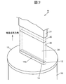
- FIG. 1 is a vertical sectional view of a part of an EFG crystal manufacturing apparatus according to an embodiment.
- FIG. 2 is a perspective view showing a state during growth of a ⁇ -Ga 2 O 3 single crystal.
- FIG. 3A is a plan view showing a substrate cut out from a ⁇ -Ga 2 O 3 single crystal and measurement positions of X-ray diffraction.
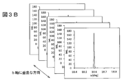
- FIG. 3B is an image diagram in which X-ray diffraction profiles obtained at each measurement point are arranged along a direction perpendicular to the b-axis.
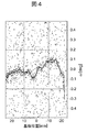
- FIG. 4 is a diagram showing the distribution of X-ray diffraction intensity for each measurement point.
- FIG. 1 is a vertical sectional view of a part of an EFG crystal manufacturing apparatus according to an embodiment.
- FIG. 2 is a perspective view showing a state during growth of a ⁇ -Ga 2 O 3 single crystal.
- FIG. 3A is a plan view showing a substrate cut out from a ⁇ -Ga
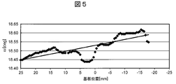
- FIG. 5 is a graph showing a curve representing the relationship between the substrate position and the peak position of the X-ray diffraction profile and its approximate straight line.
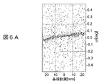
- FIG. 6A shows the distribution of X-ray diffraction intensity for each measurement point of a substrate cut out from the crystal A and centered on a point 40 mm from the seed crystal.
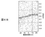
- FIG. 6B shows the X-ray diffraction intensity distribution for each measurement point of the substrate cut out from the crystal B and centered on a point 40 mm from the seed crystal.
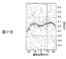
- FIG. 7A represents the distribution of X-ray diffraction intensity for each measurement point of a substrate cut out from the crystal C and centered on a point 40 mm from the seed crystal.
- FIG. 7B represents the distribution of X-ray diffraction intensity at each measurement point of the substrate cut out from the crystal D and centered on a point 40 mm from the seed crystal.
- FIG. 8 is a diagram showing variations in crystal structures in the direction perpendicular to the b-axis of crystals A and B to which Sn is added, crystals C and D to which Si is added, and crystal EF to which no additive is added.
- Embodiment in this embodiment a tabular ⁇ -Ga 2 O 3 single crystal to which Sn is added is grown in the b-axis direction using a seed crystal. Thereby, a ⁇ -Ga 2 O 3 single crystal having a small variation in crystal quality in the direction perpendicular to the b-axis direction can be obtained.
- Si is used as a conductive impurity added to the Ga 2 O 3 crystal.
- Si has a relatively low vapor pressure at the growth temperature of the Ga 2 O 3 single crystal among the conductive impurities added to the Ga 2 O 3 crystal, and the amount of evaporation during crystal growth is small. It is relatively easy to control the conductivity of the Ga 2 O 3 crystal.
- Sn has a higher vapor pressure at the growth temperature of the Ga 2 O 3 single crystal than Si and has a large amount of evaporation during crystal growth, so it is a little difficult to treat as a conductive impurity added to the Ga 2 O 3 crystal.
- the inventors of the present application have found that the crystal structure in the b-axis direction is constant by adding Si under the specific condition of growing a flat ⁇ -Ga 2 O 3 single crystal in the b-axis direction. However, it has been found that there is a large variation in the crystal structure in the direction perpendicular to the b-axis. The inventors of the present application have found that the problem can be solved by adding Sn instead of Si.
- a method in the case of using an edge-defined film-fed growth (EFG) method will be described.
- the growth method of the flat ⁇ -Ga 2 O 3 single crystal of the present embodiment is not limited to the EFG method, and other growth methods such as a pulling-down method such as a micro PD (pulling-down) method are used. May be.
- a plate-like ⁇ -Ga 2 O 3 single crystal may be grown by applying a die having a slit like a die of the EFG method to the Bridgeman method.
- FIG. 1 is a vertical sectional view of a part of the EFG crystal manufacturing apparatus according to the present embodiment.
- the EFG crystal manufacturing apparatus 10 includes a crucible 13 for receiving a Ga 2 O 3 melt 12, a die 14 having a slit 14 a installed in the crucible 13, and a die 14 including an opening 14 b of the slit 14 a.
- a lid 15 that closes the upper surface of the crucible 13 so as to expose the upper part, a seed crystal holder 21 that holds a ⁇ -Ga 2 O 3 -based seed crystal (hereinafter referred to as “seed crystal”) 20, and a seed crystal holder And a shaft 22 that supports 21 so as to be movable up and down.
- seed crystal ⁇ -Ga 2 O 3 -based seed crystal
- the crucible 13 contains a Ga 2 O 3 melt 12 obtained by dissolving a Ga 2 O 3 powder.
- the crucible 13 is made of a material such as iridium having heat resistance that can accommodate the Ga 2 O 3 melt 12.
- the die 14 has a slit 14a for raising the Ga 2 O 3 melt 12 by capillary action.
- the lid 15 prevents the high-temperature Ga 2 O 3 melt 12 from evaporating from the crucible 13 and further prevents the vapor of the Ga 2 O 3 melt 12 from adhering to a portion other than the upper surface of the slit 14a. .
- crystal orientation of the ⁇ -Ga 2 O 3 single crystal 25 is equal to the crystal orientation of the seed crystal 20, in order to control the crystal orientation of the ⁇ -Ga 2 O 3 single crystal 25 is, for example, the bottom surface of the seed crystal 20 Adjust the plane orientation and angle in the horizontal plane.
- FIG. 2 is a perspective view showing a state during growth of a ⁇ -Ga 2 O 3 single crystal.
- a surface 26 in FIG. 2 is a main surface of the ⁇ -Ga 2 O 3 single crystal 25 parallel to the slit direction of the slit 14a. If cut out ⁇ -Ga 2 O 3 single crystal 25 is grown to form a ⁇ -Ga 2 O 3 system board, the plane orientation of the desired major surface of the ⁇ -Ga 2 O 3 based substrate beta-Ga The plane orientation of the face 26 of the 2 O 3 single crystal 25 is matched. For example, in the case of forming a ⁇ -Ga 2 O 3 based substrate having the ( ⁇ 201) plane as the main surface, the plane orientation of the plane 26 is set to ( ⁇ 201).
- the grown ⁇ -Ga 2 O 3 single crystal 25 can be used as a seed crystal for growing a new ⁇ -Ga 2 O 3 single crystal.
- the crystal growth direction shown in FIGS. 1 and 2 is a direction (b-axis direction) parallel to the b-axis of the ⁇ -Ga 2 O 3 single crystal 25.
- the ⁇ -Ga 2 O 3 single crystal 25 and the seed crystal 20 are a ⁇ -Ga 2 O 3 single crystal or a Ga 2 O 3 single crystal to which an element such as Al or In is added.
- it is a ⁇ -Ga 2 O 3 single crystal to which Al and In are added (Ga x Al y In (1-xy) ) 2 O 3 (0 ⁇ x ⁇ 1, 0 ⁇ y ⁇ 1, 0 ⁇ x + y ⁇ 1)
- a single crystal may be used.
- Al is added, the band gap is widened, and when In is added, the band gap is narrowed.
- An amount of Sn raw material is added to the ⁇ -Ga 2 O 3 type raw material such that Sn having a desired concentration is added.
- SnO 2 is added in such an amount that Sn with a concentration of 0.005 mol% or more and 1.0 mol% or less is added.
- concentration is less than 0.005 mol%, sufficient characteristics as a conductive substrate cannot be obtained.
- it exceeds 1.0 mol% problems such as a decrease in doping efficiency, an increase in absorption coefficient, and a decrease in yield are likely to occur.
- the ⁇ -Ga 2 O 3 based single crystal 25 is grown in a nitrogen atmosphere.
- a seed crystal 20 having a horizontal cross section substantially the same size as the Ga 2 O 3 single crystal 25 is used.
- the shoulder widening process for expanding the width of the Ga 2 O 3 single crystal 25 is not performed, twinning that tends to occur in the shoulder widening process can be suppressed.
- the seed crystal 20 is larger than the seed crystal used for normal crystal growth and is vulnerable to thermal shock, the seed crystal 20 from the die 14 before contacting with the Ga 2 O 3 melt 12 is high.
- the thickness is preferably low to some extent, for example, 10 mm.
- the descending speed of the seed crystal 20 until it contacts with the Ga 2 O 3 melt 12 is preferably low to some extent, for example, 1 mm / min.
- the stand-by time until the seed crystal 20 is pulled after contacting the seed crystal 20 with the Ga 2 O 3 melt 12 is preferably long to some extent in order to stabilize the temperature and prevent thermal shock, for example, 10 minutes.
- the rate of temperature rise when melting the raw material in the crucible 13 is preferably low to some extent in order to prevent the temperature around the crucible 13 from rising rapidly and causing thermal shock to the seed crystal 20. Melt.
- a substrate is cut out from a seed crystal of ⁇ -Ga 2 O 3 -based single crystal grown using the above method, and after mirror polishing, the crystal quality is evaluated by X-ray diffraction measurement. This crystal quality is evaluated by evaluating the variation in crystal structure in the direction perpendicular to the b-axis of the substrate.
- FIG. 3A is a plan view showing a substrate cut out from a ⁇ -Ga 2 O 3 single crystal and measurement positions of X-ray diffraction.
- the substrate with the b-axis direction of the ⁇ -Ga 2 O 3 single crystal as the axis at the measurement points arranged along the direction perpendicular to the b axis of the ⁇ -Ga 2 O 3 single crystal indicated by “ ⁇ ” in FIG. 3A
- the X-ray diffraction intensity is measured while rotating to obtain an X-ray diffraction profile.
- the rotation angle about the b-axis direction of the substrate is ⁇ [deg].
- FIG. 3B is an image diagram in which X-ray diffraction profiles obtained at each measurement point are arranged along a direction perpendicular to the b-axis.
- FIG. 4 is a view of FIG. 3B as viewed from above, and represents the distribution of X-ray diffraction intensity at each measurement point.
- the horizontal axis in FIG. 4 represents the position [mm] on the substrate in the direction perpendicular to the b-axis, and the vertical axis represents the rotation angle ⁇ [deg] of the substrate.
- the region where the dot density is high is a region where the X-ray diffraction intensity is high, and the curve connects the peak positions of the X-ray diffraction profile at each measurement point. Note that the position on the substrate on the horizontal axis is the origin of the center of the substrate.
- FIG. 5 is a graph showing a curve representing the relationship between the substrate position and the peak position of the X-ray diffraction profile and an approximate straight line obtained from the linear approximation by the least square method.
- the horizontal axis in FIG. 5 represents the position [mm] on the substrate in the direction perpendicular to the b-axis, and the vertical axis represents the rotation angle ⁇ [deg] of the substrate.
- the difference between the peak position of the X-ray diffraction profile at each substrate position and the rotation angle ⁇ of the approximate line is obtained, and the average value ⁇ is obtained.
- two ⁇ -Ga 2 O 3 based single crystals having a main surface of ( ⁇ 201) are grown by adding Si at a concentration of 0.05 mol% (crystals C and D).
- the substrate centering on the point where the position from the seed crystal is 40 mm was cut out from these crystals C and D.
- the diameter of each substrate was 50 mm.
- crystals E and F two ⁇ -Ga 2 O 3 -based single crystals having a main surface of ( ⁇ 201) without growing a dopant were grown (referred to as crystals E and F). From the crystals E and F, a substrate centered around a point 40 mm from the seed crystal and a substrate centered at a point 90 mm from the seed crystal were cut out one by one. The diameter of each substrate was 50 mm.
- the width of the flat crystals A to F was set to 52 mm in order to cut out a substrate having a diameter of 50 mm.
- 6A and 6B show distributions of X-ray diffraction intensity for each measurement point of the substrate centered on a point 40 mm from the seed crystal, cut out from crystals A and B, respectively.
- 7A and 7B show the distribution of X-ray diffraction intensity at each measurement point on a substrate centered on a point 40 mm from the seed crystal, cut out from crystals C and D, respectively.
- 6A, 6B, 7A, and 7B correspond to FIG.
- FIGS. 6A, 6B, 7A, and 7B show that the substrate cut from the crystals A and B to which Sn is added is perpendicular to the b-axis than the substrate cut from the crystals C and D to which Si is added. This shows that the variation in the peak position of the X-ray diffraction profile in one direction is small and the variation in the crystal structure in the direction perpendicular to the b-axis is small.
- FIG. 8 is a diagram showing variations in crystal structures in a direction perpendicular to the b-axis of crystals A and B to which Sn is added, crystals C and D to which Si is added, and crystal EF to which no additive is added.
- the vertical axis in FIG. 8 represents the ratio of ⁇ to ⁇ of the seed crystal in each crystal. As the ⁇ ratio is smaller, the crystal structure variation in the direction perpendicular to the b-axis is closer to that of the seed crystal, indicating that a high-quality crystal is obtained.
- the upper part of the character column arranged along the horizontal axis in the lower part of FIG. 8 represents the type of crystal cut out from the substrate (crystals A to F), and the middle part represents the type of added dopant (Si, Sn, none).
- the lower row represents the distance (40 mm, 90 mm) from the seed crystal at the center of the substrate before being cut out from the crystal.
- FIG. 8 shows that the ⁇ ratio of the crystals A and B to which Sn is added is smaller than the ⁇ ratio of the crystals C and D to which Si is added, and the crystal structure variation in the direction perpendicular to the b-axis of the crystals A and B Is small.
- the ⁇ ratio of the crystals A and B to which Sn is added is close to the ⁇ ratio of the crystals E and F to which no additive is added, and is in a direction perpendicular to the b-axis of the ⁇ -Ga 2 O 3 single crystal to which Sn is added. It shows that the variation in crystal structure is close to that of an additive-free ⁇ -Ga 2 O 3 single crystal.
- the crystal quality is lower in a region farther from the seed crystal, but b in a region where the distance from the seed crystal of the crystals A and B to which Sn is added is 90 mm.
- the variation in the crystal structure in the direction perpendicular to the axis is smaller than that in the region where the distance from the seed crystal of crystals C and D to which Si is added is 40 mm. This indicates that by adding Sn instead of Si, variation in the crystal structure in the direction perpendicular to the b-axis of the ⁇ -Ga 2 O 3 single crystal can be greatly reduced.
- the effect of the present embodiment does not depend on the Sn addition concentration, and the variation in the crystal structure in the direction perpendicular to the b-axis of the ⁇ -Ga 2 O 3 single crystal is substantially unchanged up to at least 1.0 mol%. It has been confirmed.
- a ⁇ -Ga 2 O 3 single crystal growth method capable of growing a high-quality ⁇ -Ga 2 O 3 single crystal having a small variation in crystal structure in the b-axis direction.
Landscapes
- Chemical & Material Sciences (AREA)
- Engineering & Computer Science (AREA)
- Crystallography & Structural Chemistry (AREA)
- Materials Engineering (AREA)
- Metallurgy (AREA)
- Organic Chemistry (AREA)
- Inorganic Chemistry (AREA)
- Crystals, And After-Treatments Of Crystals (AREA)
Abstract
結晶構造のばらつきが小さい高品質のβ-Ga2O3系単結晶をb軸方向に成長させることのできるβ-Ga2O3系単結晶の成長方法を提供する。 一実施の形態において、種結晶を用いて、Snが添加された平板状のβ-Ga2O3系単結晶をb軸方向に成長させる工程を含む、β-Ga2O3系単結晶の成長方法を提供する。
Description
本発明は、β-Ga2O3系単結晶の成長方法に関する。
従来、EFG(Edge-defined Film-fed Growth)法を用いた平板状のGa2O3単結晶の成長方法が知られている(例えば、特許文献1参照)。
特許文献1によれば、SiO2をドーパント原料として用いて、SiをGa2O3単結晶に添加する。SiO2は、Ga2O3との融点の差が小さく、Ga2O3単結晶の成長温度(Ga2O3単結晶の原料の融点)における蒸気圧が低いため、Ga2O3単結晶中のドーパント量の制御が容易である。
また、従来、FZ(Floating Zone)法を用いた円柱状のβ-Ga2O3系単結晶の成長方法が知られている(例えば、特許文献2参照)。
特許文献2によれば、Si、Sn、Zr、Hf、Ge等を熱融解性調整用添加物としてβ-Ga2O3系単結晶に添加する。熱融解性調整用添加物を添加することにより、β-Ga2O3系単結晶の赤外線吸収特性が大きくなり、FZ装置の光源からの赤外線をβ-Ga2O3系単結晶が効率的に吸収するようになる。このため、β-Ga2O3系単結晶の外径が大きい場合であっても、中心部と外側の温度差が小さくなり、中心部が凝固し難くなる。
本発明の目的の1つは、結晶構造のばらつきが小さい高品質のβ-Ga2O3系単結晶をb軸方向に成長させることのできるβ-Ga2O3系単結晶の成長方法を提供することである。
本発明の一態様は、上記目的を達成するために、[1]~[3]のβ-Ga2O3系単結晶の成長方法を提供する。
[1]種結晶を用いて、Snが添加された平板状のβ-Ga2O3系単結晶をb軸方向に成長させる工程を含む、β-Ga2O3系単結晶の成長方法。
[2]EFG法により前記β-Ga2O3系単結晶を成長させる、前記[1]に記載のβ-Ga2O3系単結晶の成長方法。
[3]前記β-Ga2O3系単結晶への前記Snの添加濃度が0.005mol%以上かつ1.0mol%以下である、前記[1]又は[2]に記載のβ-Ga2O3系単結晶の成長方法。
本発明によれば、結晶構造のばらつきが小さい高品質のβ-Ga2O3系単結晶をb軸方向に成長させることのできるβ-Ga2O3系単結晶の成長方法を提供することができる。
〔実施の形態〕
本実施の形態においては、種結晶を用いて、Snが添加された平板状のβ-Ga2O3系単結晶をb軸方向に成長させる。これにより、b軸方向に垂直な方向の結晶品質のばらつきが小さいβ-Ga2O3系単結晶を得ることができる。
本実施の形態においては、種結晶を用いて、Snが添加された平板状のβ-Ga2O3系単結晶をb軸方向に成長させる。これにより、b軸方向に垂直な方向の結晶品質のばらつきが小さいβ-Ga2O3系単結晶を得ることができる。
従来、多くの場合、Ga2O3結晶に添加される導電型不純物として、Siが用いられている。SiはGa2O3結晶に添加される導電型不純物の中でGa2O3単結晶の成長温度における蒸気圧が比較的低く、結晶成長中の蒸発量が少ないため、Si添加量の調整によるGa2O3結晶の導電性の制御が比較的容易である。
一方、SnはSiよりもGa2O3単結晶の成長温度における蒸気圧が高く、結晶成長中の蒸発量が多いため、Ga2O3結晶に添加される導電型不純物としては少々扱いづらい。
しかしながら、本願の発明者等は、平板状のβ-Ga2O3系単結晶をb軸方向に成長させるという特定の条件下において、Siを添加することにより、b軸方向の結晶構造は一定になるが、b軸に垂直な方向の結晶構造に大きなばらつきが生じるという問題を見出した。そして、本願の発明者等は、Siの代わりにSnを添加することにより、その問題を解消できることを見出した。
(β-Ga2O3系単結晶の成長)
以下に、平板状のβ-Ga2O3系単結晶を成長させる方法の一例として、EFG(Edge-defined film-fed growth)法を用いる場合の方法について説明する。なお、本実施の形態の平板状のβ-Ga2O3系単結晶の成長方法はEFG法に限られず、他の成長方法、例えば、マイクロPD(pulling-down)法等の引き下げ法を用いてもよい。また、ブリッジマン法にEFG法のダイのようなスリットを有するダイを適用し、平板状のβ-Ga2O3系単結晶を育成してもよい。
以下に、平板状のβ-Ga2O3系単結晶を成長させる方法の一例として、EFG(Edge-defined film-fed growth)法を用いる場合の方法について説明する。なお、本実施の形態の平板状のβ-Ga2O3系単結晶の成長方法はEFG法に限られず、他の成長方法、例えば、マイクロPD(pulling-down)法等の引き下げ法を用いてもよい。また、ブリッジマン法にEFG法のダイのようなスリットを有するダイを適用し、平板状のβ-Ga2O3系単結晶を育成してもよい。
図1は、本実施の形態に係るEFG結晶製造装置の一部の垂直断面図である。このEFG結晶製造装置10は、Ga2O3系融液12を受容するルツボ13と、このルツボ13内に設置されたスリット14aを有するダイ14と、スリット14aの開口部14bを含むダイ14の上部を露出させるようにルツボ13の上面を閉塞する蓋15と、β-Ga2O3系種結晶(以下、「種結晶」という)20を保持する種結晶保持具21と、種結晶保持具21を昇降可能に支持するシャフト22とを有する。
ルツボ13は、Ga2O3系粉末を溶解させて得られたGa2O3系融液12を収容する。ルツボ13は、Ga2O3系融液12を収容しうる耐熱性を有するイリジウム等の材料からなる。
ダイ14は、Ga2O3系融液12を毛細管現象により上昇させるためのスリット14aを有する。
蓋15は、ルツボ13から高温のGa2O3系融液12が蒸発することを防止し、さらにスリット14aの上面以外の部分にGa2O3系融液12の蒸気が付着することを防ぐ。
種結晶20を下降させて、スリット14aの開口部14bからダイ14の上面に広がったGa2O3系融液12に接触させ、Ga2O3系融液12と接触した種結晶20を引き上げることにより、平板状のβ-Ga2O3系単結晶25を成長させる。β-Ga2O3系単結晶25の結晶方位は種結晶20の結晶方位と等しく、β-Ga2O3系単結晶25の結晶方位を制御するためには、例えば、種結晶20の底面の面方位及び水平面内の角度を調整する。
図2は、β-Ga2O3系単結晶の成長中の様子を表す斜視図である。図2中の面26は、スリット14aのスリット方向と平行なβ-Ga2O3系単結晶25の主面である。成長させたβ-Ga2O3系単結晶25を切り出してβ-Ga2O3系基板を形成する場合は、β-Ga2O3系基板の所望の主面の面方位にβ-Ga2O3系単結晶25の面26の面方位を一致させる。例えば、(-201)面を主面とするβ-Ga2O3系基板を形成する場合は、面26の面方位を(-201)とする。また、成長させたβ-Ga2O3系単結晶25は、新たなβ-Ga2O3系単結晶を成長させるための種結晶として用いることができる。図1、2に示される結晶成長方向は、β-Ga2O3系単結晶25のb軸に平行な方向(b軸方向)である。
β-Ga2O3系単結晶25及び種結晶20は、β-Ga2O3単結晶、又は、Al、In等の元素が添加されたGa2O3単結晶である。例えば、Al及びInが添加されたβ-Ga2O3単結晶である(GaxAlyIn(1-x-y))2O3(0<x≦1、0≦y≦1、0<x+y≦1)単結晶であってもよい。Alを添加した場合にはバンドギャップが広がり、Inを添加した場合にはバンドギャップが狭くなる。
β-Ga2O3系原料に、所望の濃度のSnが添加されるような量のSn原料を加える。例えば、LED用基板を切り出すためのβ-Ga2O3系単結晶25を成長させる場合は、濃度0.005mol%以上かつ1.0mol%以下のSnが添加されるような量のSnO2をβ-Ga2O3系原料に加える。濃度0.005mol%未満の場合、導電性基板として十分な特性が得られない。また、1.0mol%を超える場合、ドーピング効率の低下、吸収係数増加、歩留低下等の問題が生じやすい。
以下に、本実施の形態のβ-Ga2O3系単結晶25の育成条件の一例について述べる。
例えば、β-Ga2O3系単結晶25の育成は、窒素雰囲気下で行われる。
図1、2に示される例では、水平断面の大きさがGa2O3系単結晶25とほぼ同じ大きさの種結晶20を用いている。この場合、Ga2O3系単結晶25の幅を広げる肩広げ工程を行わないため、肩広げ工程において発生しやすい双晶化を抑えることができる。
なお、この場合、種結晶20は通常の結晶育成に用いられる種結晶よりも大きく、熱衝撃に弱いため、Ga2O3系融液12に接触させる前の種結晶20のダイ14からの高さは、ある程度低いことが好ましく、例えば、10mmである。また、Ga2O3系融液12に接触させるまでの種結晶20の降下速度は、ある程度低いことが好ましく、例えば、1mm/minである。
種結晶20をGa2O3系融液12に接触させた後の引き上げるまでの待機時間は、温度をより安定させて熱衝撃を防ぐために、ある程度長いことが好ましく、例えば、10minである。
ルツボ13中の原料を溶かすときの昇温速度は、ルツボ13周辺の温度が急上昇して種結晶20に熱衝撃が加わることを防ぐために、ある程度低いことが好ましく、例えば、11時間掛けて原料を溶かす。
(β-Ga2O3系単結晶の品質評価方法)
上記の方法等を用いて成長させたβ-Ga2O3系単結晶の種結晶から基板を切り出し、鏡面研磨した後、X線回折測定により結晶品質の評価を行う。この結晶品質の評価は、基板のb軸に垂直な方向の結晶構造のばらつきの評価により行う。
上記の方法等を用いて成長させたβ-Ga2O3系単結晶の種結晶から基板を切り出し、鏡面研磨した後、X線回折測定により結晶品質の評価を行う。この結晶品質の評価は、基板のb軸に垂直な方向の結晶構造のばらつきの評価により行う。
図3Aは、β-Ga2O3系単結晶から切り出した基板とX線回折の測定位置を表す平面図である。図3Aに「×」で示されるβ-Ga2O3系単結晶のb軸に垂直な方向に沿って並ぶ測定点において、β-Ga2O3系単結晶のb軸方向を軸として基板を回転させながらX線回折強度を測定し、X線回折プロファイルを得る。ここで、基板のb軸方向を軸とする回転角度をω[deg]とする。
図3Bは、各測定点において得られたX線回折プロファイルをb軸に垂直な方向に沿って並べたイメージ図である。
図4は、図3Bを上方から見た図であり、測定点ごとのX線回折強度の分布を表す。図4の横軸はb軸に垂直な方向の基板上の位置[mm]、縦軸は基板の回転角度ω[deg]を表す。ドットの密度の高い領域がX線回折強度の高い領域であることを表し、曲線は各測定点におけるX線回折プロファイルのピーク位置を繋いだものである。なお、横軸の基板上の位置は、基板の中心を原点としている。
図5は、基板位置とX線回折プロファイルのピーク位置の関係を表す曲線とその最小二乗法による線形近似から求められた近似直線を表すグラフである。図5の横軸はb軸に垂直な方向の基板上の位置[mm]、縦軸は基板の回転角度ω[deg]を表す。
図5から、各々の基板位置におけるX線回折プロファイルのピーク位置と近似直線の回転角度ωの差を求め、それらの平均値αを求める。b軸に垂直な方向のX線回折プロファイルのピーク位置のばらつきが小さいほど、このαが小さくなり、基板のb軸に垂直な方向の結晶構造のばらつきが小さいことを意味する。
(β-Ga2O3系単結晶の品質評価結果)
本実施の形態の一例として、濃度0.05mol%のSnを添加して主面が(-201)面の平板状のβ-Ga2O3系単結晶を2つ成長させ(結晶A、Bとする)、これら結晶A、Bから、種結晶からの位置が40mmの点を中心とする基板と、種結晶からの位置が90mmの点を中心とする基板をそれぞれ1枚ずつ切り出した。各基板の直径は50mmとした。
本実施の形態の一例として、濃度0.05mol%のSnを添加して主面が(-201)面の平板状のβ-Ga2O3系単結晶を2つ成長させ(結晶A、Bとする)、これら結晶A、Bから、種結晶からの位置が40mmの点を中心とする基板と、種結晶からの位置が90mmの点を中心とする基板をそれぞれ1枚ずつ切り出した。各基板の直径は50mmとした。
同様に、比較例として、濃度0.05mol%のSiを添加して主面が(-201)面の平板状のβ-Ga2O3系単結晶を2つ成長させ(結晶C、Dとする)、これら結晶C、Dから、種結晶からの位置が40mmの点を中心とする基板をそれぞれ切り出した。各基板の直径は50mmとした。
また、他の比較例として、ドーパントを添加せずに主面が(-201)面の平板状のβ-Ga2O3系単結晶を2つ成長させ(結晶E、Fとする)、これら結晶E、Fから、種結晶からの位置が40mmの点を中心とする基板と、種結晶からの位置が90mmの点を中心とする基板をそれぞれ1枚ずつ切り出した。各基板の直径は50mmとした。
なお、平板状の結晶A~Fの幅(結晶成長方向に垂直な幅)は、直径50mmの基板を切り出すため、52mmとした。
上記の4枚のSn添加β-Ga2O3系単結晶基板、2枚のSi添加β-Ga2O3系単結晶基板、及び4枚の無添加β-Ga2O3系単結晶基板に対し、上記の評価方法により、基板のb軸に垂直な方向の結晶構造のばらつきを評価した。
図6A、図6Bは、結晶A、Bからそれぞれ切り出された、種結晶からの位置が40mmの点を中心とする基板の、測定点ごとのX線回折強度の分布を表す。また、図7A、図7Bは、結晶C、Dからそれぞれ切り出された、種結晶からの位置が40mmの点を中心とする基板の、測定点ごとのX線回折強度の分布を表す。図6A、図6B、図7A、図7Bは、図4に対応する。
図6A、図6B、図7A、図7Bは、Snが添加された結晶A、Bから切り出された基板は、Siが添加された結晶C、Dから切り出された基板よりも、b軸に垂直な方向のX線回折プロファイルのピーク位置のばらつきが小さく、b軸に垂直な方向の結晶構造のばらつきが小さいことを示している。
図8は、Snが添加された結晶A、B、Siが添加された結晶C、D、及び無添加の結晶EFの、b軸に垂直な方向の結晶構造のばらつきを示す図である。図8の縦軸は、各々の結晶におけるαの種結晶のαに対する比を表す。このα比が小さいほど、b軸に垂直な方向の結晶構造のばらつきが種結晶のものに近く、高品質の結晶が得られていることを示す。
図8の下部の横軸に沿って並んだ文字欄の上段は基板を切り出した結晶の種類(結晶A~F)を表し、中段は添加されたドーパントの種類(Si、Sn、なし)を表し、下段は結晶から切り出される前の基板の中心の種結晶からの距離(40mm、90mm)を表す。
図8は、Snが添加された結晶A、Bのα比が、Siが添加された結晶C、Dのα比よりも小さく、結晶A、Bのb軸に垂直な方向の結晶構造のばらつきが小さいことを示している。また、Snが添加された結晶A、Bのα比は、無添加の結晶E、Fのα比と近く、Snを添加したβ-Ga2O3系単結晶のb軸に垂直な方向の結晶構造のばらつきが無添加のβ-Ga2O3系単結晶のものに近いことを示している。
また、一般的に、成長させた結晶においては、種結晶からの距離が離れた領域ほど結晶品質が低いが、Snが添加された結晶A、Bの種結晶からの距離が90mmの領域のb軸に垂直な方向の結晶構造のばらつきは、Siが添加された結晶C、Dの種結晶からの距離が40mmの領域のものよりも小さい。これは、Siの代わりにSnを添加することにより、β-Ga2O3系単結晶のb軸に垂直な方向の結晶構造のばらつきを大きく低減できることを表している。
なお、同様の評価方法により、b軸方向の結晶構造のばらつきを評価したところ、Snを添加したβ-Ga2O3系単結晶、Siを添加したβ-Ga2O3系単結晶ともに、b軸方向の結晶構造のばらつきはほとんど見られなかった。
(実施の形態の効果)
本実施の形態によれば、β-Ga2O3系単結晶に導電性を与えるドーパントとしてSnを用いることにより、結晶構造のばらつきが小さい高品質のβ-Ga2O3系単結晶をb軸方向に成長させることができる。
本実施の形態によれば、β-Ga2O3系単結晶に導電性を与えるドーパントとしてSnを用いることにより、結晶構造のばらつきが小さい高品質のβ-Ga2O3系単結晶をb軸方向に成長させることができる。
一例として、Snを添加して、長さ65mm、幅52mm以上の平板状のβ-Ga2O3系単結晶を成長させることにより、種結晶からの距離が40mmの点を中心とする領域から、直径50mmの結晶品質に優れた導電性基板を得ることができる。
なお、本実施の形態の効果はSnの添加濃度には依らず、少なくとも1.0mol%まではβ-Ga2O3系単結晶のb軸に垂直な方向の結晶構造のばらつきがほぼ変化しないことが確認されている。
以上、本発明の実施の形態を説明したが、本発明は、上記実施の形態に限定されず、発明の主旨を逸脱しない範囲内において種々変形実施が可能である。
また、上記に記載した実施の形態は特許請求の範囲に係る発明を限定するものではない。また、実施の形態の中で説明した特徴の組合せの全てが発明の課題を解決するための手段に必須であるとは限らない点に留意すべきである。
結晶構造のばらつきが小さい高品質のβ-Ga2O3系単結晶をb軸方向に成長させることのできるβ-Ga2O3系単結晶の成長方法を提供する。
10…EFG結晶製造装置、 20…種結晶、 25…β-Ga2O3系単結晶
Claims (3)
- 種結晶を用いて、Snが添加された平板状のβ-Ga2O3系単結晶をb軸方向に成長させる工程を含む、
β-Ga2O3系単結晶の成長方法。 - EFG法により前記β-Ga2O3系単結晶を成長させる、
請求項1に記載のβ-Ga2O3系単結晶の成長方法。 - 前記β-Ga2O3系単結晶への前記Snの添加濃度が0.005mol%以上かつ1.0mol%以下である、
請求項1又は2に記載のβ-Ga2O3系単結晶の成長方法。
Priority Applications (3)
| Application Number | Priority Date | Filing Date | Title |
|---|---|---|---|
| CN201480020148.XA CN105102694A (zh) | 2013-04-04 | 2014-03-31 | β-Ga2O3系单晶的生长方法 |
| EP14779805.2A EP2990509B1 (en) | 2013-04-04 | 2014-03-31 | Method for growing beta-ga2o3-based single crystal |
| US14/782,039 US10526721B2 (en) | 2013-04-04 | 2014-03-31 | Method for growing β-GA2O3-based single crystal |
Applications Claiming Priority (2)
| Application Number | Priority Date | Filing Date | Title |
|---|---|---|---|
| JP2013-078575 | 2013-04-04 | ||
| JP2013078575A JP5788925B2 (ja) | 2013-04-04 | 2013-04-04 | β−Ga2O3系単結晶の成長方法 |
Publications (1)
| Publication Number | Publication Date |
|---|---|
| WO2014163056A1 true WO2014163056A1 (ja) | 2014-10-09 |
Family
ID=51658352
Family Applications (1)
| Application Number | Title | Priority Date | Filing Date |
|---|---|---|---|
| PCT/JP2014/059572 Ceased WO2014163056A1 (ja) | 2013-04-04 | 2014-03-31 | β-Ga2O3系単結晶の成長方法 |
Country Status (6)
| Country | Link |
|---|---|
| US (1) | US10526721B2 (ja) |
| EP (1) | EP2990509B1 (ja) |
| JP (1) | JP5788925B2 (ja) |
| CN (1) | CN105102694A (ja) |
| TW (1) | TWI634241B (ja) |
| WO (1) | WO2014163056A1 (ja) |
Cited By (1)
| Publication number | Priority date | Publication date | Assignee | Title |
|---|---|---|---|---|
| WO2024078704A1 (en) | 2022-10-11 | 2024-04-18 | Forschungsverbund Berlin E.V. | MELT-GROWN BULK ß-(AlxGa1-x)2O3 SINGLE CRYSTALS AND METHOD FOR PRODUCING BULK ß-(AlxGA1-x)2O3 SINGLE CRYSTALS |
Families Citing this family (7)
| Publication number | Priority date | Publication date | Assignee | Title |
|---|---|---|---|---|
| JP5865867B2 (ja) | 2013-05-13 | 2016-02-17 | 株式会社タムラ製作所 | β−Ga2O3系単結晶の育成方法、並びにβ−Ga2O3系単結晶基板の製造方法 |
| CN107541776A (zh) * | 2017-08-14 | 2018-01-05 | 同济大学 | 一种大尺寸氧化镓单晶的生长设备及方法 |
| JP7222669B2 (ja) * | 2018-11-16 | 2023-02-15 | 株式会社タムラ製作所 | 単結晶育成方法、種結晶、及び単結晶 |
| JP7436978B2 (ja) * | 2019-10-28 | 2024-02-22 | Agc株式会社 | 単結晶インゴット、結晶育成用ダイ、及び単結晶の製造方法 |
| JP2022147882A (ja) * | 2021-03-24 | 2022-10-06 | アダマンド並木精密宝石株式会社 | Ga2O3系単結晶基板と、Ga2O3系単結晶基板の製造方法 |
| KR102660564B1 (ko) * | 2021-12-29 | 2024-04-25 | 한국세라믹기술원 | Efg용 잉곳 성장장치 |
| KR102731513B1 (ko) * | 2022-11-14 | 2024-11-18 | 한국세라믹기술원 | 산화갈륨 단결정 성장용 분말 및 이의 제조방법 |
Citations (3)
| Publication number | Priority date | Publication date | Assignee | Title |
|---|---|---|---|---|
| JP2004262684A (ja) * | 2003-02-24 | 2004-09-24 | Univ Waseda | β−Ga2O3系単結晶成長方法 |
| JP2005235961A (ja) * | 2004-02-18 | 2005-09-02 | Univ Waseda | Ga2O3系単結晶の導電率制御方法 |
| JP2006312571A (ja) * | 2005-05-09 | 2006-11-16 | Koha Co Ltd | Ga2O3系結晶の製造方法 |
Family Cites Families (9)
| Publication number | Priority date | Publication date | Assignee | Title |
|---|---|---|---|---|
| JP4083396B2 (ja) * | 2000-07-10 | 2008-04-30 | 独立行政法人科学技術振興機構 | 紫外透明導電膜とその製造方法 |
| JP3679097B2 (ja) * | 2002-05-31 | 2005-08-03 | 株式会社光波 | 発光素子 |
| WO2004074556A2 (ja) * | 2003-02-24 | 2004-09-02 | Waseda University | β‐Ga2O3系単結晶成長方法、薄膜単結晶の成長方法、Ga2O3系発光素子およびその製造方法 |
| JP2006273684A (ja) * | 2005-03-30 | 2006-10-12 | Koha Co Ltd | Iii族酸化物系単結晶の製造方法 |
| JP2008037725A (ja) * | 2006-08-10 | 2008-02-21 | Nippon Light Metal Co Ltd | 酸化ガリウム単結晶の製造方法 |
| JP2008156141A (ja) * | 2006-12-21 | 2008-07-10 | Koha Co Ltd | 半導体基板及びその製造方法 |
| JP5786179B2 (ja) | 2010-03-12 | 2015-09-30 | 並木精密宝石株式会社 | 酸化ガリウム単結晶及びその製造方法 |
| US9461124B2 (en) | 2011-09-08 | 2016-10-04 | Tamura Corporation | Ga2O3 semiconductor element |
| JP5491483B2 (ja) | 2011-11-15 | 2014-05-14 | 株式会社タムラ製作所 | β−Ga2O3系単結晶の成長方法 |
-
2013
- 2013-04-04 JP JP2013078575A patent/JP5788925B2/ja active Active
-
2014
- 2014-03-31 WO PCT/JP2014/059572 patent/WO2014163056A1/ja not_active Ceased
- 2014-03-31 US US14/782,039 patent/US10526721B2/en active Active
- 2014-03-31 CN CN201480020148.XA patent/CN105102694A/zh active Pending
- 2014-03-31 EP EP14779805.2A patent/EP2990509B1/en active Active
- 2014-04-03 TW TW103112566A patent/TWI634241B/zh active
Patent Citations (3)
| Publication number | Priority date | Publication date | Assignee | Title |
|---|---|---|---|---|
| JP2004262684A (ja) * | 2003-02-24 | 2004-09-24 | Univ Waseda | β−Ga2O3系単結晶成長方法 |
| JP2005235961A (ja) * | 2004-02-18 | 2005-09-02 | Univ Waseda | Ga2O3系単結晶の導電率制御方法 |
| JP2006312571A (ja) * | 2005-05-09 | 2006-11-16 | Koha Co Ltd | Ga2O3系結晶の製造方法 |
Cited By (1)
| Publication number | Priority date | Publication date | Assignee | Title |
|---|---|---|---|---|
| WO2024078704A1 (en) | 2022-10-11 | 2024-04-18 | Forschungsverbund Berlin E.V. | MELT-GROWN BULK ß-(AlxGa1-x)2O3 SINGLE CRYSTALS AND METHOD FOR PRODUCING BULK ß-(AlxGA1-x)2O3 SINGLE CRYSTALS |
Also Published As
| Publication number | Publication date |
|---|---|
| TWI634241B (zh) | 2018-09-01 |
| EP2990509A1 (en) | 2016-03-02 |
| JP5788925B2 (ja) | 2015-10-07 |
| US10526721B2 (en) | 2020-01-07 |
| US20160032485A1 (en) | 2016-02-04 |
| TW201443301A (zh) | 2014-11-16 |
| CN105102694A (zh) | 2015-11-25 |
| EP2990509A4 (en) | 2017-01-18 |
| JP2014201480A (ja) | 2014-10-27 |
| EP2990509B1 (en) | 2019-12-18 |
Similar Documents
| Publication | Publication Date | Title |
|---|---|---|
| JP5788925B2 (ja) | β−Ga2O3系単結晶の成長方法 | |
| TWI601856B (zh) | β-Ga 2 O 3 Department of single crystal growth method | |
| JP5864998B2 (ja) | β−Ga2O3系単結晶の成長方法 | |
| TWI651442B (zh) | GaO系單晶基板及其製造方法 | |
| JP5756075B2 (ja) | β−Ga2O3系単結晶の育成方法 | |
| EP2767621B1 (en) | Method for producing b-ga2o3 substrate and method for producing crystal laminate structure | |
| TWI677602B (zh) | β-GaO系單晶基板 | |
| JP4723071B2 (ja) | シリコン結晶及びシリコン結晶ウエーハ並びにその製造方法 | |
| DE112013001054T5 (de) | Verfahren zum Herstellen eines Silizium-Einkristall-Wafers | |
| US9988739B2 (en) | Method for pulling a single crystal composed of silicon from a melt contained in a crucible, and single crystal produced thereby | |
| EP3387166A1 (de) | Halbleiterscheibe aus einkristallinem silizium und verfahren zu deren herstellung | |
| DE60036359T2 (de) | Verbesserter silizium werkstoff vom typ-n für epitaxie-substrat und verfahren zu seiner herstellung | |
| CN116988158A (zh) | 一种高品质碳化硅衬底及半导体器件 | |
| JP2014205618A (ja) | β−Ga2O3系単結晶及び基板 | |
| JP2009292654A (ja) | シリコン単結晶引上げ方法 | |
| JP2005206391A (ja) | シリコン単結晶基板の抵抗率保証方法及びシリコン単結晶基板の製造方法並びにシリコン単結晶基板 | |
| JP7536916B2 (ja) | 単結晶 | |
| JP5282762B2 (ja) | シリコン単結晶の製造方法 | |
| JP5777756B2 (ja) | β−Ga2O3系単結晶基板 | |
| JP2011046565A (ja) | 単結晶シリコンインゴット、単結晶シリコンウェハ、単結晶シリコン太陽電池セル、および単結晶シリコンインゴットの製造方法 | |
| JP2014503452A (ja) | 多レーンの炉内で成長させられる半導体結晶性シートの抵抗率の範囲を縮小する方法 | |
| JP5688654B2 (ja) | シリコン結晶、シリコン結晶の製造方法およびシリコン多結晶インゴットの製造方法 | |
| CN121006598A (zh) | 一种具有双热输运行为的Cs3Bi2I9单晶材料及其制备方法与应用 | |
| JP4193681B2 (ja) | リン化ガリウム単結晶製造装置 |
Legal Events
| Date | Code | Title | Description |
|---|---|---|---|
| WWE | Wipo information: entry into national phase |
Ref document number: 201480020148.X Country of ref document: CN |
|
| 121 | Ep: the epo has been informed by wipo that ep was designated in this application |
Ref document number: 14779805 Country of ref document: EP Kind code of ref document: A1 |
|
| WWE | Wipo information: entry into national phase |
Ref document number: 14782039 Country of ref document: US |
|
| NENP | Non-entry into the national phase |
Ref country code: DE |
|
| WWE | Wipo information: entry into national phase |
Ref document number: 2014779805 Country of ref document: EP |