WO2014168096A1 - 回転型セミバッチald装置およびプロセス - Google Patents
回転型セミバッチald装置およびプロセス Download PDFInfo
- Publication number
- WO2014168096A1 WO2014168096A1 PCT/JP2014/060027 JP2014060027W WO2014168096A1 WO 2014168096 A1 WO2014168096 A1 WO 2014168096A1 JP 2014060027 W JP2014060027 W JP 2014060027W WO 2014168096 A1 WO2014168096 A1 WO 2014168096A1
- Authority
- WO
- WIPO (PCT)
- Prior art keywords
- ald
- aspect ratio
- time
- substrate
- saturation
- Prior art date
- Legal status (The legal status is an assumption and is not a legal conclusion. Google has not performed a legal analysis and makes no representation as to the accuracy of the status listed.)
- Ceased
Links
Images


Classifications
-
- C—CHEMISTRY; METALLURGY
- C23—COATING METALLIC MATERIAL; COATING MATERIAL WITH METALLIC MATERIAL; CHEMICAL SURFACE TREATMENT; DIFFUSION TREATMENT OF METALLIC MATERIAL; COATING BY VACUUM EVAPORATION, BY SPUTTERING, BY ION IMPLANTATION OR BY CHEMICAL VAPOUR DEPOSITION, IN GENERAL; INHIBITING CORROSION OF METALLIC MATERIAL OR INCRUSTATION IN GENERAL
- C23C—COATING METALLIC MATERIAL; COATING MATERIAL WITH METALLIC MATERIAL; SURFACE TREATMENT OF METALLIC MATERIAL BY DIFFUSION INTO THE SURFACE, BY CHEMICAL CONVERSION OR SUBSTITUTION; COATING BY VACUUM EVAPORATION, BY SPUTTERING, BY ION IMPLANTATION OR BY CHEMICAL VAPOUR DEPOSITION, IN GENERAL
- C23C16/00—Chemical coating by decomposition of gaseous compounds, without leaving reaction products of surface material in the coating, i.e. chemical vapour deposition [CVD] processes
- C23C16/44—Chemical coating by decomposition of gaseous compounds, without leaving reaction products of surface material in the coating, i.e. chemical vapour deposition [CVD] processes characterised by the method of coating
- C23C16/455—Chemical coating by decomposition of gaseous compounds, without leaving reaction products of surface material in the coating, i.e. chemical vapour deposition [CVD] processes characterised by the method of coating characterised by the method used for introducing gases into reaction chamber or for modifying gas flows in reaction chamber
- C23C16/45523—Pulsed gas flow or change of composition over time
- C23C16/45525—Atomic layer deposition [ALD]
- C23C16/45544—Atomic layer deposition [ALD] characterized by the apparatus
- C23C16/45548—Atomic layer deposition [ALD] characterized by the apparatus having arrangements for gas injection at different locations of the reactor for each ALD half-reaction
- C23C16/45551—Atomic layer deposition [ALD] characterized by the apparatus having arrangements for gas injection at different locations of the reactor for each ALD half-reaction for relative movement of the substrate and the gas injectors or half-reaction reactor compartments
-
- C—CHEMISTRY; METALLURGY
- C23—COATING METALLIC MATERIAL; COATING MATERIAL WITH METALLIC MATERIAL; CHEMICAL SURFACE TREATMENT; DIFFUSION TREATMENT OF METALLIC MATERIAL; COATING BY VACUUM EVAPORATION, BY SPUTTERING, BY ION IMPLANTATION OR BY CHEMICAL VAPOUR DEPOSITION, IN GENERAL; INHIBITING CORROSION OF METALLIC MATERIAL OR INCRUSTATION IN GENERAL
- C23C—COATING METALLIC MATERIAL; COATING MATERIAL WITH METALLIC MATERIAL; SURFACE TREATMENT OF METALLIC MATERIAL BY DIFFUSION INTO THE SURFACE, BY CHEMICAL CONVERSION OR SUBSTITUTION; COATING BY VACUUM EVAPORATION, BY SPUTTERING, BY ION IMPLANTATION OR BY CHEMICAL VAPOUR DEPOSITION, IN GENERAL
- C23C16/00—Chemical coating by decomposition of gaseous compounds, without leaving reaction products of surface material in the coating, i.e. chemical vapour deposition [CVD] processes
- C23C16/44—Chemical coating by decomposition of gaseous compounds, without leaving reaction products of surface material in the coating, i.e. chemical vapour deposition [CVD] processes characterised by the method of coating
- C23C16/4412—Details relating to the exhausts, e.g. pumps, filters, scrubbers, particle traps
-
- C—CHEMISTRY; METALLURGY
- C23—COATING METALLIC MATERIAL; COATING MATERIAL WITH METALLIC MATERIAL; CHEMICAL SURFACE TREATMENT; DIFFUSION TREATMENT OF METALLIC MATERIAL; COATING BY VACUUM EVAPORATION, BY SPUTTERING, BY ION IMPLANTATION OR BY CHEMICAL VAPOUR DEPOSITION, IN GENERAL; INHIBITING CORROSION OF METALLIC MATERIAL OR INCRUSTATION IN GENERAL
- C23C—COATING METALLIC MATERIAL; COATING MATERIAL WITH METALLIC MATERIAL; SURFACE TREATMENT OF METALLIC MATERIAL BY DIFFUSION INTO THE SURFACE, BY CHEMICAL CONVERSION OR SUBSTITUTION; COATING BY VACUUM EVAPORATION, BY SPUTTERING, BY ION IMPLANTATION OR BY CHEMICAL VAPOUR DEPOSITION, IN GENERAL
- C23C16/00—Chemical coating by decomposition of gaseous compounds, without leaving reaction products of surface material in the coating, i.e. chemical vapour deposition [CVD] processes
- C23C16/44—Chemical coating by decomposition of gaseous compounds, without leaving reaction products of surface material in the coating, i.e. chemical vapour deposition [CVD] processes characterised by the method of coating
- C23C16/455—Chemical coating by decomposition of gaseous compounds, without leaving reaction products of surface material in the coating, i.e. chemical vapour deposition [CVD] processes characterised by the method of coating characterised by the method used for introducing gases into reaction chamber or for modifying gas flows in reaction chamber
- C23C16/45561—Gas plumbing upstream of the reaction chamber
-
- C—CHEMISTRY; METALLURGY
- C23—COATING METALLIC MATERIAL; COATING MATERIAL WITH METALLIC MATERIAL; CHEMICAL SURFACE TREATMENT; DIFFUSION TREATMENT OF METALLIC MATERIAL; COATING BY VACUUM EVAPORATION, BY SPUTTERING, BY ION IMPLANTATION OR BY CHEMICAL VAPOUR DEPOSITION, IN GENERAL; INHIBITING CORROSION OF METALLIC MATERIAL OR INCRUSTATION IN GENERAL
- C23C—COATING METALLIC MATERIAL; COATING MATERIAL WITH METALLIC MATERIAL; SURFACE TREATMENT OF METALLIC MATERIAL BY DIFFUSION INTO THE SURFACE, BY CHEMICAL CONVERSION OR SUBSTITUTION; COATING BY VACUUM EVAPORATION, BY SPUTTERING, BY ION IMPLANTATION OR BY CHEMICAL VAPOUR DEPOSITION, IN GENERAL
- C23C16/00—Chemical coating by decomposition of gaseous compounds, without leaving reaction products of surface material in the coating, i.e. chemical vapour deposition [CVD] processes
- C23C16/44—Chemical coating by decomposition of gaseous compounds, without leaving reaction products of surface material in the coating, i.e. chemical vapour deposition [CVD] processes characterised by the method of coating
- C23C16/455—Chemical coating by decomposition of gaseous compounds, without leaving reaction products of surface material in the coating, i.e. chemical vapour deposition [CVD] processes characterised by the method of coating characterised by the method used for introducing gases into reaction chamber or for modifying gas flows in reaction chamber
- C23C16/45563—Gas nozzles
- C23C16/45565—Shower nozzles
-
- C—CHEMISTRY; METALLURGY
- C23—COATING METALLIC MATERIAL; COATING MATERIAL WITH METALLIC MATERIAL; CHEMICAL SURFACE TREATMENT; DIFFUSION TREATMENT OF METALLIC MATERIAL; COATING BY VACUUM EVAPORATION, BY SPUTTERING, BY ION IMPLANTATION OR BY CHEMICAL VAPOUR DEPOSITION, IN GENERAL; INHIBITING CORROSION OF METALLIC MATERIAL OR INCRUSTATION IN GENERAL
- C23C—COATING METALLIC MATERIAL; COATING MATERIAL WITH METALLIC MATERIAL; SURFACE TREATMENT OF METALLIC MATERIAL BY DIFFUSION INTO THE SURFACE, BY CHEMICAL CONVERSION OR SUBSTITUTION; COATING BY VACUUM EVAPORATION, BY SPUTTERING, BY ION IMPLANTATION OR BY CHEMICAL VAPOUR DEPOSITION, IN GENERAL
- C23C16/00—Chemical coating by decomposition of gaseous compounds, without leaving reaction products of surface material in the coating, i.e. chemical vapour deposition [CVD] processes
- C23C16/44—Chemical coating by decomposition of gaseous compounds, without leaving reaction products of surface material in the coating, i.e. chemical vapour deposition [CVD] processes characterised by the method of coating
- C23C16/52—Controlling or regulating the coating process
Definitions
- the present invention relates to an atomic layer deposition apparatus and process for providing high-quality film formation with high production last name, gas-saving consumption and high quality in the manufacture of electronic devices such as semiconductors, flat panels, solar cells or LEDs.
- ALD atomic layer deposition
- ALD is attracting attention as a key technique.
- a silicon oxide film having a thickness of 10 to 20 nm is formed on the patterned resist film at a temperature of about 200 ° C. or less at which the organic resist film does not deteriorate. It is necessary to form a film, and as introduced in Non-Patent Document 5, development of mass production technology is actively promoted as a solution for the SiO 2 film ALD technology. Further, when manufacturing a low power consumption semiconductor mounted on a portable terminal or a tablet PC, formation of a High-k / Metal gate by ALD technology is an indispensable technology.
- ALD In semiconductor manufacturing, in addition to these processes, DRAM capacitor upper and lower electrode formation using metals such as TiN and Ru (Non-Patent Documents 6 to 10), gate electrode sidewall formation using SiN, contacts and through-holes
- metals such as TiN and Ru (Non-Patent Documents 6 to 10)
- ALD application processes have been developed, such as barrier seed formation, NAND flash memory high-k insulating film formation, and charge trap film formation, and are expected to become increasingly important technologies in the future. Even for flat panels, LEDs, and solar cells, ALD, which has a high step coverage and can be processed at a low temperature, is beginning to be considered for use in forming an ITO film or a passivation film.
- ALD film forming apparatuses Conventionally, single-wafer ALD apparatuses and batch furnace apparatuses have been mainstream as ALD film forming apparatuses.
- a single-wafer ALD apparatus is widely used as one chamber.
- the batch furnace ALD apparatus is most popularly used for forming a high-k insulating film of a DRAM capacitor.
- the number of substrates processed per hour is about 20 WPH (Wafers Per Hour) or less per system, and productivity is extremely low compared to other film forming techniques.
- productivity is extremely low compared to other film forming techniques. This is because atomic layers are deposited in layers by introducing each gas into the process chamber alternately by opening and closing each gas valve so that the metal-containing source gas and non-metal gases such as ozone do not cross in the reaction vessel. This is an essential defect of switching type ALD.
- one ALD cycle consists of eight steps of vacuum exhaust, Ti precursor supply, vacuum exhaust, purge gas supply, vacuum exhaust, NH 3 supply, vacuum exhaust, and purge gas supply, Each step requires a total of about 1 second to open and close the valve, stabilize the process chamber pressure and perform each reaction, and it takes about several seconds to complete one ALD cycle.
- the amount of increase in TiN film thickness per unit ALD cycle is about 0.1 nm in the 1/4 TiN layer due to steric hindrance between precursors.
- a process time of several hundred seconds is required, and the throughput per process chamber is only about four per hour. Even if the film forming apparatus system includes four process chambers, the throughput is about 16 sheets.
- a process chamber furnace can be filled with about 100 substrates. However, since the capacity of the chamber furnace is several tens of times, the time required for gas supply and evacuation is several tens of times. The cycle time usually requires a few minutes. If gas supply / evacuation is performed at a higher speed than this, gas replacement becomes incomplete, and particles are generated by the reaction between the mixed gases. Therefore, even in batch ALD using a furnace, it takes several hours to deposit a TiN film having a thickness of 10 nm, and the throughput is about a dozen or so per hour, which is equivalent to single-wafer ALD.
- Stacked ALD is a method of depositing several single-wafer ALD process chambers in the vertical direction and switching all the chambers at the same timing as seen in, for example, Patent Document 1 or 2.
- the throughput is improved several times as compared with the single-wafer ALD chamber, but since the apparatus manufacturing cost is increased, it has not been used in earnest.
- the rotary semi-batch ALD apparatus is composed of a rotary table in which a plurality of substrates to be processed are mounted in an arc shape, and a plurality of reaction gas and purge gas supply means arranged in a fan shape in the upper space thereof. By rotating, each substrate is sequentially exposed to each gas to advance the ALD process.
- High-speed film formation is possible because there is no gas switching and gas switching associated with vacuum evacuation, which is essential in the conventional switching type ALD, and the manufacturing cost of the apparatus can be kept relatively low because a switching gas valve is unnecessary. .
- mass production development of this rotary semi-batch ALD is being actively promoted.
- the first rotary semi-batch ALD apparatus was filed in 1990 by US Pat. Therein, a large cylindrical vacuum vessel is divided into a total of four fan-shaped sub-chambers of two reaction gas chambers and two purge gas chambers disposed between them, and a reaction gas supply means is provided above the center of each sub-chamber. Is arranged, and the gas exhaust part is installed at the lower part of the two purge gas chambers. By rotating the disk-shaped table, a plurality of substrates to be processed on the table pass through each sub-chamber and ALD film formation is performed. This invention became the prototype of the subsequent rotary semi-batch ALD apparatus.
- the rotary semi-batch ALD can be roughly classified into four types according to the method of separating the reaction gas.
- the first is a partition separation type ALD apparatus, as in Patent Document 3, in which a vacuum vessel is divided into relatively large sub-chambers by partition walls so that the flow of reaction gas or purge gas in each sub-chamber is uniform.
- the gas supply and exhaust methods are devised.
- Patent Documents 4 to 7 are specific examples.
- an evacuation chamber is disposed between the reaction gas subchambers so that the reaction gas flows uniformly from the reaction gas subchamber toward the evacuation chamber.
- Patent Document 5 a purge gas chamber is provided between the reaction gas chambers, and the purge gas is flowed from the center to the peripheral direction to improve the reaction gas separation characteristics. Furthermore, in patent document 6, gas separation performance is improved by ejecting purge gas from the partition surrounding the reaction gas subchamber.
- these partition wall-separated ALD apparatuses have a large sub-chamber volume and cannot sufficiently reduce the drift and retention of the reaction gas. Therefore, it is impossible to completely solve the problem of coverage reduction and particle problems in Patent Document 1. difficult.
- Patent Document 7 the vacuum vessel is divided into four sub-chambers, and the gas supply means connected to each sub-chamber is provided with a switching function capable of supplying gas, reaction gas or purge gas in a pulsed manner.
- One sub-chamber can be used as a reaction chamber or a purge chamber. According to this means, the gas separation performance is improved, and it is possible to stack polyatomic components by changing the kind of the reaction gas. However, since gas exhaust and supply are required with gas switching, the ALD cycle time becomes extremely long.
- the second rotary semi-batch ALD apparatus is a gas curtain type ALD apparatus, in which the purge gas flows between the reaction gas supply means like a curtain to reduce the mixing of the reaction gas.
- Patent documents 8 to 11 are specific examples.
- purge gas is allowed to flow from top to bottom to prevent reaction gas mixing.
- a purge gas is flowed from bottom to top to form a gas curtain.
- reaction gas nozzles and purge gas nozzles are alternately installed radially and rotated, so that the reaction gas and purge gas are alternately supplied to each substrate.
- the third type of rotary semi-batch ALD device is a microreactor type ALD device that combines both gas supply and discharge functions into a compact square reactor with a width of several centimeters, and that reaction gas leaks out of the reactor. By preventing this, the gas separation function is improved.
- a good gas separation characteristic is achieved by installing a large number of reactors, supplying different reaction gases and purge gases to the respective reactors, and exhausting the reactors at the adjacent portions. Specific examples thereof are Patent Documents 12 to 15. Patent Document 12 was filed for an invention in 1979 and has become a prototype of a microreactor.
- the first reactive gas nozzle, the first purge gas nozzle, the second reactive gas nozzle, and the second purge gas nozzle each have a structure that is linearly arranged via the exhaust port.
- Patent Document 13 has a structure in which a plurality of rectangular microreactors having a single gas supply / exhaust function are radially arranged in a vacuum vessel.
- the reactive gas as an etching gas, not only film formation, but also etching, film formation pretreatment, film modification after film formation, and the like are possible.
- the first reaction gas nozzle, the first purge gas nozzle, the second reaction gas nozzle, the second purge gas nozzle, and the exhaust port installed between the nozzles become one compact fan-type ALD reactor.
- Patent Document 15 A large number are arranged radially and continuously.
- the first reaction gas is filled in a large vacuum vessel, and the second reaction gas and the purge gas are supplied / discharged from a plurality of rectangular microreactors installed in a radial pattern.
- the first reaction gas microreactor is unnecessary, and the structure is simplified.
- the trade-off between productivity and step coverage becomes more severe than other methods.
- the width of the microreactor is narrower than other methods. For example, if the width of one gas nozzle is several centimeters, even if the rotational speed is about 30 RPM, the exposure time to the reaction gas will be about tens of milliseconds or less, and sufficient exposure time necessary for the ALD reaction will be secured. Since it becomes impossible, the step coverage will be reduced.
- the second reaction gas not containing metal requires a time of about 100 milliseconds or more to perform ALD film formation, and this short exposure time is a serious problem.
- the rotation speed is decreased to increase the exposure time, and an attempt is made to improve productivity by arranging a larger number of microreactors.
- productivity is rather decreased.
- the reason will be described below.
- the ALD process the relationship between the exposure time of the substrate to be processed and the deposition rate in a single ALD cycle is as shown in FIG. It is known that when the exposure time exceeds a certain time, it is saturated and becomes a constant value. This saturation phenomenon corresponds to a state in which all adsorption reaction sites on the surface of the substrate to be processed are covered with the reaction gas.
- the time when the film formation rate starts to be saturated is defined as the ALD saturation reaction time, and the film formation rate is A region that is saturated and constant can be defined as an ALD saturation reaction region.
- a film with a thickness of A nm can be formed in a single ALD process
- the throughput W can be represented by 60 nqra / A (WPH).
- each microreactor requires a minimum gas separation, and when the number of microreactors q is increased, the area occupied by the gas separation region in the reaction gas supply unit relatively increases, and the contact time with the reaction gas correspondingly increases. Becomes shorter. For this reason, the trade-off between throughput and step coverage becomes more severe.
- the type of the fourth rotary type semi-batch ALD apparatus is a narrow gap gas dispersion type ALD apparatus, which is composed of a pair of first and second reaction gas supply units and a purge gas region installed between them, and a gas supply gas nozzle.
- a dispersion plate or using a shower plate By attaching a dispersion plate or using a shower plate, the reaction gas and the purge gas are devised so as to flow uniformly in a narrow gap space between the gas nozzle and the substrate. This method can be operated at a higher speed than the microreactor method and is expected to improve productivity.
- a series of inventions in Patent Documents 16 to 21 and Patent Document 22 are specific examples. In the series of inventions of Patent Documents 16 to 21, a gas dispersion plate is installed adjacent to the reaction gas and the purge gas.
- the purge gas temperature is increased, the circumferential length of the second gas reactive gas dispersion plate is made longer than the circumferential length of the first reactive gas dispersion plate, the gas nozzle ejection holes are directed forward, the purge gas
- Various contrivances have been made to make the gas flow uniform, such as installing a rectifying plate near the reactive gas nozzle and optimizing the position of the exhaust hole.
- a fan-shaped shower plate is used in place of the reactive gas and purge gas gas nozzles, and a narrow gas exhaust region is provided between each shower plate, and gas is produced from a small number of exhaust holes. Yes.
- these narrow gap gas dispersion type ALD means have a drawback that although the throughput is high, the amount of gas used is as high as several tens of SLM, and the cost of consumer goods is high.
- these gas dispersion means have a drawback that the reaction gas utilization efficiency remains at about 0.5% or less, and 99.5% or more of the reaction gas is exhausted without being used.
- this high gas flow causes new problems. That is, when a large amount of gas flow is generated in one direction on the substrate to be processed, a pressure difference is generated between both ends of the substrate, and thereby the substrate is lifted. The problem is that the substrate to be processed is likely to float especially when a film having a high compressive stress is formed. When the substrate rises, the substrate hits the upper gas supply unit, and the substrate is damaged. As described above, when gas flows in one direction at a large flow rate on the substrate to be processed, a serious problem is caused in terms of process reliability of the manufacturing apparatus.
- a table holding a substrate to be processed is rotated at a high speed of about 300 revolutions per minute in order to increase productivity.
- the exposure time of the substrate to the reaction gas is within 100 milliseconds, and the ALD saturation reaction region is not reached as shown by point C in FIG. In this case, the problem that the step coverage is reduced becomes serious for trenches and holes having a high aspect ratio.
- the present invention solves the problems of the rotary semi-batch ALD apparatus described above, and provides a technique that enables a rotary semi-batch ALD apparatus and a process with high throughput, low particles, low gas consumption and high coverage. Is.
- the present invention relates to a vacuum vessel, a rotating susceptor, a plurality of substrates to be processed mounted on the susceptor, a substrate heater installed immediately below the substrate to be processed, and a plurality of fan-shaped reaction gases installed above the vacuum vessel It comprises a supply means, a purge gas supply means for separating a reaction gas installed between the reaction gas means, and a vacuum exhaust means provided in a separate system for each gas supply means, and rotating the susceptor
- the invention is based on the following five new discoveries. Remarkable effects can be obtained with each single invention, but the effect is further improved by combining two or more.
- the at least one reactive gas supply means is constituted by a shower plate for jetting gas uniformly, a cavity for downflow of gas, and a partition wall surrounding the cavity.
- the gas supply means is optimized by configuring the space with a shower plate with a narrow gap so that it can flow evenly at a high flow rate in the lateral direction in the space between the substrate to be processed and the productivity and step coverage characteristics are improved.
- Improved rotary semi-batch ALD device Improved rotary semi-batch ALD device.
- Rotating semi-batch ALD with improved gas separation characteristics by having a structure surrounded by a vacuum exhaust groove so that the reaction gas and purge gas can be locally exhausted independently for all reaction gas and purge gas supply means. apparatus.
- each reactive gas supply / exhaust means By disposing each reactive gas supply / exhaust means to be larger than the diameter of the substrate to be processed so that both gas supply means do not come on the same substrate, low particle generation characteristics and gas separation characteristics can be obtained. Improved rotary semi-batch ALD device.
- the air bearing mechanism by the purge gas gas supply means is provided in the upper gas supply means or the rotating susceptor in combination with other holding means such as a spring, and the gap between the lower end of the upper gas supply means and the substrate to be processed is accurately controlled.
- a rotary semi-batch ALD device that reduces the amount of gas used.
- a rotating semi-batch ALD apparatus and its ALD sequence wherein the same number of ALD cycles are applied to all substrates to be processed for the same time.
- ALD saturation reaction time is calculated based on the maximum aspect ratio (ratio of depth to the width of the hole or trench) of the pattern formed on the surface shape of the substrate to be processed, and the surface of the substrate to be processed is the saturation reaction calculation time.
- a rotary semi-batch ALD device that achieves both high step coverage and high productivity by controlling the substrate rotation speed so that it is exposed to the reaction gas for a longer time.
- the ALD reaction proceeds by alternately exposing the substrate to be processed to a metal-containing reaction gas and a non-metal reaction gas.
- the ALD reaction of TiN by TiCl 4 and NH 3 can be expressed by the following two-step reaction.
- the metal-containing reaction gas is usually an organometallic compound or a metal halogen compound, and a substance having a vapor pressure at the processing temperature equal to or higher than the process pressure is selected.
- metals Si, Ti, Hf, Zr, Ru, Ta, Sr, etc. are usually used in semiconductor manufacturing, but are not particularly limited in the present invention, and are selected according to atoms constituting the target film. Just do it.
- nonmetal reactive gas ozone, O 2 , NH 3 , N 2 , H 2 or the like is used depending on the film forming material.
- These non-metal reactive gases are not limited by the present invention, and may be selected depending on the atoms constituting the target film.
- TiCl 4 which is a metal-containing reaction gas
- NH which is a nonmetal gas adsorbed in the lower layer
- NH mainly by van der Waals force, according to reaction formula 1, and then Lewis acid. It is chemically bonded to the nitrogen atom by a base reaction.
- the metal-containing reaction gas molecule has a large molecular diameter and cannot be adsorbed to all nitrogen atoms due to steric hindrance.
- metal-containing gas molecules are adsorbed at a rate of about 1 nitrogen atom in 4 nitrogen atoms.
- the ammonia gas molecule NH 3 which is a non-metal reaction gas, chemically reacts with the adsorbed —N—Ti—Cl to bond with Ti atoms.
- Both reactions in Reaction Schemes 1 and 2 are chemisorption reactions involving recombination of bonds on the substrate surface, and HCl is produced as a reaction product.
- the reaction of this second step However, a larger activation energy is required compared with the reaction in the first step. For this reason, in most ALD reactions, the second step shown in Reaction Scheme 2 will rate-limit the overall ALD reaction.
- the reaction rate R2 of the reaction formula 2 can be expressed by the following formula.
- R 2 k 2 (1- ⁇ ) P NH 3 ⁇ k ⁇ 2 ⁇ P HCl (Formula 1)
- ⁇ represents the ratio of reaction adsorption sites on the surface of —N—Ti—Cl (a) where NH 3 gas is not chemically adsorbed.
- K 2 and k ⁇ 2 represent the reaction rate constants of the progress reaction (adsorption reaction) and the reverse progress reaction (elimination reaction) of the second step reaction, and P NH3 and P HCl are the partial pressures of NH 3 gas and HCl gas. Indicates.
- ⁇ k 2 P NH 3 / (k 2 P NH 3 + k ⁇ 2 P HCl ) (Formula 2)
- ⁇ k 2 P NH 3 / (k 2 P NH 3 + k ⁇ 2 P HCl )
- the ALD reaction proceeds only by exposure. This result was found to be applicable not only to TiN ALD deposition but also to most ALD processes. It was also found that the reaction involving the metal-containing reaction gas shown in Reaction Formula 1 has a similar reaction mechanism.
- the reaction gas is composed of a shower plate comprising uniform gas ejection holes with a narrow pitch, and the ejected reaction gas is gently dispersed.
- a cavity for uniformly supplying the substrate to be processed by downflow and a substantially vertical partition wall surrounding the cavity were decided.
- the unreacted gas and the reaction product gas remaining in the ultrafine hole or trench pattern having a dimension of about 10 mm carved on the surface of the substrate to be processed are about 100 ms or less which is a normal exposure time. It is necessary to discharge completely in a short time. In this case, it was found that the slow down flow is inappropriate, and it is desirable to increase the gas flow rate of the purge gas flowing on the substrate to be processed as much as possible at all the positions on the substrate.
- the gas density is 1.5 ⁇ 10 16 cm ⁇ 3 and the nitrogen gas diffusion flux to the substrate to be processed is 3 ⁇ 10 20 cm ⁇ 2 s ⁇ 1 .
- the rotation speed of the substrate to be processed is 30 revolutions per minute and the area ratio of one purge gas supply unit in the gas supply means is 1/8, the purge gas exposure time of the substrate to be processed in one purge gas supply unit is 250 ms. During this period, the number of nitrogen gas molecules flowing into a hole with a diameter of 32 nm and an aspect ratio of 100 per second by diffusion becomes 5 ⁇ 10 8 s ⁇ 1 .
- the number of residual reaction gases inside the hole can be calculated to be about 40. Therefore, while the target substrate is in contact with the purge gas, 107 times the nitrogen gas of the residual gas molecules will be flowing into the hole, in a normal rotation semibatch type ALD apparatus, the purge gas exposure time is the rotational speed There is almost no bottleneck, and the exposure time to the reaction gas is rate-limiting. However, if the reactive gas remains in the purge gas space, the residual reactive gas molecules enter the hole again, and the replacement effect is reduced.
- the spatial gap between the substrate to be processed is made as small as possible to increase the lateral purge gas flow rate and improve the reaction gas replacement effect by the purge gas.
- the gas flow is biased and stays, and the gas replacement becomes incomplete.
- the gas ejection holes it is desirable to install the gas ejection holes at a distance within several times the average free path of the purge gas.
- the pressure of the ALD process is almost 0.1 torr or more, and the mean free path of nitrogen molecules at that pressure is within 2 mm.
- the purge gas ejection means has a uniform pitch of 10 mm or less.
- Adopt a shower plate structure arranged in This narrow gap and narrow pitch shower plate structure speeds up the purge gas flow at all positions on the substrate surface, reduces the concentration of unreacted gas and reaction product gas on the substrate surface, and improves replacement and discharge efficiency.
- a shower plate for at least one reaction gas supply means, a shower plate for discharging gas uniformly, a cavity for downflow of gas, and
- the purge gas supply means is constituted by a narrow gap shower plate for allowing the purge gas to flow uniformly at a high flow rate in the lateral direction in the space between the substrate to be processed.
- the fan-shaped reaction gas supply means and the purge gas supply means are all surrounded by a separate vacuum exhaust groove.
- each reaction gas is discharged from the bottom of the vacuum vessel through a gap between the rotary susceptor and the vacuum vessel wall.
- the reaction gas is mixed in the lower part of the vacuum vessel and the exhaust line to generate particles. Further, the reaction gas and the purge gas are mixed, and the gas separation effect is low.
- an evacuation groove is provided between the reaction gas nozzle and the purge gas nozzle, so that a higher gas separation effect and lower particle performance can be obtained.
- an evacuation groove is provided only between the reaction gas supply unit and the adjacent purge gas supply unit, and independent vacuum evacuation grooves are provided on the center side and the outer peripheral side of the reaction gas supply unit, respectively. Therefore, when it rotates at high speed, a part of the reaction gas flows toward the outer periphery and leaks from the microreactor.
- the vacuum exhaust groove is installed not only between the fan-type reaction gas supply unit and the purge gas supply unit, but also on the reaction gas supply center side, the reaction gas supply unit outer periphery side, and not only on the reaction gas supply unit but also on the purge gas supply unit.
- the particle generation and gas separation effect were investigated. As a result, it has been found that the vacuum exhaust grooves on the center side and the outer peripheral side play an important role in gas separation, like the vacuum exhaust grooves between the reaction gas supply unit and the purge gas supply unit. It has also been found that if an evacuation groove is also provided on the outer periphery of the purge gas supply unit, the occurrence of gas flow in one direction is suppressed, so that the disturbance between gases can be reduced and the gas separation effect is further improved.
- the step of determining the productivity of the ALD process is the contact time between the reaction gas, particularly the nonmetal reaction gas, and the substrate, and the contact time between the purge gas and the substrate to be processed is usually not the step of determining the ALD reaction. . Therefore, in the upper gas supply means, it is desirable to make the occupation area of the purge gas supply section as small as possible and to make the occupation area of the reaction gas supply section as large as possible. However, if the occupation area of the purge gas supply unit is excessively reduced, the gas separation effect of the metal reactive gas and the non-metallic reactive gas is reduced, and both reactive gases are mixed to generate particles.
- the width at the middle part of the fan-type purge gas supply / exhaust means is changed to 1/4, 1/2, 3/4, 4/4 of the diameter of the substrate to be processed, and the increase in particles of the substrate to be processed at this time is measured. did.
- no increase in particles was observed on the surface of the substrate to be processed even when the intermediate width of the purge supply / exhaust means was 1/4 of the diameter of the substrate to be processed.
- an increase in particles was clearly observed when the number of processed sheets exceeded 1000. Even if the intermediate width of the purge gas supply / exhaust means was increased to 1/2 or 3/4 of the substrate diameter, a large particle reduction effect was not observed.
- the rotating susceptor and the gas supply means disposed on the upper part thereof have a diameter of 1 meter or more and a weight of tens of kilograms or more. A considerable amount of shape distortion occurs. For this reason, it is desirable to control the gap within several millimeters, but it is not easy to always control within several millimeters during the ALD process. To solve this problem, the patent document relating to the conventional rotary semi-batch ALD apparatus does not provide an effective solution.
- a single or multiple laser light sources are attached to the upper gas supply means, the target substrate is irradiated with laser light, and the phase difference between incident light and reflected light is detected.
- a method is conceivable in which the distance to the substrate to be processed is optically measured and the measured value is fed back in real time to a stepping motor that drives the rotary susceptor up and down.
- the conversion between the rotational motion of the stepping motor and the vertical motion of the susceptor is performed by a worm gear, a planetary gear, a rack and pinion gear, or the like. Since the rotation accuracy of a stepping motor is usually extremely accurate at about 0.05 °, the gap can be controlled with an accuracy of about several millimeters.
- Patent Document 23 a technique has been developed that improves the stable floating retention characteristics in the gap by alternately arranging gas discharge holes and gas discharge holes.
- the weight that can float is only about 1.3 g / cm 2 , and cannot support an upper gas supply means of several tens of kilograms or more.
- a technique for floating a heavy object there is a method using a spring or a magnet.
- the upper gas supply means is suspended and held by a flexible holding means such as a spring, a magnet, and / or a flexible flange, and the purge gas supply part of the upper gas supply means is provided with an air cushion function, It is possible to provide a gap control means with high accuracy within a few millimeters on the substrate surface.
- the ALD process has higher film thickness uniformity than other film forming methods such as CVD, the ALD process is mainly used for a critical process for forming a high-quality thin film having a thickness of about 10 nm or less and affecting device performance.
- the film thickness increases stepwise for each ALD cycle, and the film thickness increase amount per single ALD cycle is usually about 0.1 to 0.2 nm. Therefore, in many ALD processes, the number of ALD cycles is about several tens to 100.
- the rotary semi-batch ALD apparatus a plurality of substrates to be processed are simultaneously formed, but each substrate is located in a different gas supply unit.
- the other substrate may be located in the purge gas supply unit, the nonmetal reaction gas supply unit, or another metal-containing reaction gas supply unit.
- ALD cycle histories differ depending on the substrate to be processed, and the number of ALD cycles differs between substrates to be processed or within the substrate to be processed, resulting in variations in film thickness within or between substrates.
- the deviation reaches about 3% just by shifting one ALD cycle, and the superiority of the ALD film thickness over other CVD methods is impaired.
- reaction rate of non-metallic ALD reaction described in reaction formula 2. Can be described by a primary reaction proportional to only the unadsorbed site ⁇ under a constant pressure, as shown in Formula 3.
- the reaction rate R 2 By expressing the reaction rate R 2 as d ⁇ / dt and solving the differential equation, the adsorption site can be expressed as a function of time as in the following equation.
- ⁇ represents k 2 P NH 3 .
- ⁇ 1 ⁇ e ⁇ t (Formula 4)
- This saturation phenomenon also occurs in the reaction formula 1.
- This saturated adsorption characteristic is a feature of ALD in which a thin film is deposited for each atomic layer, and corresponds to the saturated ALD reaction region shown in FIG. It has been found that the ALD saturation time at which the ALD saturation reaction region starts to reach depends on the pressure, and is about several microseconds in the normal ALD pressure range.
- reaction formula 1 when the pressure of TiCl 4 is 1 Torr, the TiCl 4 reaction gas reaches the surface of the substrate to be processed by diffusion.
- This diffusion flux ⁇ TiCl4 is expressed by the following equation.
- ⁇ TiCl 4 P / (2 ⁇ mkT) 0.5 (Formula 5)
- P is the partial pressure of the TiCl 4 reactive gas.
- T and m represent the surface temperature of the substrate to be processed and the molecular weight of the reaction gas, respectively.
- k is the Boltzmann constant.
- the reaction gas flux expressed by Equation 5 is about 1 ⁇ 10 20 (1 / cm 2 s).
- the number of adsorption sites on the surface of the substrate to be processed is 1 ⁇ 10 15 (1 / cm 2 ) for most substances.
- the ALD saturation reaction time ts0 on the surface of the substrate to be processed can be shown by the ratio of the reaction gas flux and the number of surface adsorption sites.
- the saturation reaction time t s0 at the surface decreases, so the saturation reaction time Becomes longer than the saturation reaction time t s0 at the surface.
- the latest DRAM stack capacitor has a hole diameter of 30 nm or less, a depth of about 3 ⁇ m, and an aspect ratio of about 100.
- Saturated reaction time t s for hall of such very high aspect ratio as the simplest model, the gas molecules has flowed in diffuse from the inlet of the hole, to estimate the time which accounts for all the adsorption sites in the hole Can do. However, the number of adsorption sites is assumed to be the same on all sides.
- the aspect ratio is 100, it is about 2 ms.
- the ALD of TiN by TiCl 4 and NH 3 by changing the number of rotations for the hole pattern having an aspect ratio of 0 (flat surface) to 80 Film formation was performed, and the relationship between the step coverage and aspect ratio of the TiN film was investigated in detail using a scanning electron microscope and a transmission electron microscope.
- the step coverage is maintained to 1 up to a certain critical aspect ratio, but when the critical aspect ratio is exceeded, the step coverage suddenly decreases.
- the ALD saturation reaction time is calculated based on the maximum pekt ratio in the surface shape of the substrate to be processed, and the substrate rotation speed is controlled so that the substrate surface is exposed longer than the calculated saturation reaction time. .
- t s ⁇ t s0 ⁇ 2 (Formula 6)
- t s0 is a point extrapolated to a point where the aspect ratio is zero, that is, the square root of the exposure time during which the ALD reaction is maintained on a flat surface.
- the experiment in the above example includes a considerable amount of error, but this t s0 is about several tens of microseconds, and approximately matches the on-plane ALD saturation time calculated in the discussion of Equation 5.
- the aspect ratio is 80
- the saturation time is required to be 1 second or more
- the saturation time on a flat surface is 10,000 times or more, which is found to depend greatly on the aspect ratio.
- the exposure time of the reaction gas becomes about 50 ms or less, which is shorter than the saturation time. It is impossible to secure a sufficient step coverage.
- the present invention overcomes such problems and can ensure 100% step coverage.
- the saturation time is expressed by a simple linear function or a quadratic function of the aspect ratio, so if there is data on the aspect ratio and saturation time of one or two points, other aspect ratios can be easily saturated.
- a time derivation function can be obtained.
- the aspect ratio of 10 or more is ts >> ts0
- the ALD saturation reaction time is calculated as a function f ( ⁇ ) of the aspect ratio ⁇ on the basis of the maximum pect ratio in the substrate surface shape, and the substrate surface is exposed longer than the calculation time. Therefore, the present invention provides a rotary semi-batch ALD apparatus characterized in that the substrate rotation speed is controlled. Further, for a high aspect ratio pattern, f ( ⁇ ) can be approximated by a linear or quadratic function of the aspect ratio ⁇ .
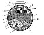
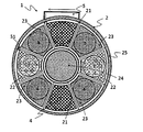
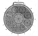
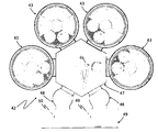
- FIG. 4 shows a plan view of the rotating semi-batch ALD apparatus of the present invention.
- a gas supply / exhaust means 2 is installed in the upper part of the vacuum vessel 1, and includes a metal-containing reaction gas supply / exhaust unit 21, a nonmetal reaction gas supply / exhaust unit 22, a purge gas supply / exhaust unit 23, and a central purge gas supply / exhaust unit 24. , And a peripheral purge gas supply / exhaust unit 25.
- the substrate 4 to be processed is placed in the recess 32 of the rotating susceptor 3 so that the surface of the substrate 4 to be processed and the surface of the susceptor 3 have the same height. It is installed.
- the rotating susceptor 3 on which the substrate to be processed 4 is mounted is counterclockwise as viewed from above as indicated by an arrow in FIG. 4 by a rotation drive motor 37 through a rotating gear 36 around a rotating shaft 34. Although it rotates in the direction, it may be clockwise.
- the rotating shaft 34 is vacuum shielded by a magnetic fluid shield 35.
- the metal-containing reaction gas supply / exhaust unit 21, the non-metal gas supply / exhaust unit 22, and the two purge gas supply / exhaust units 23 arranged between them both have a fan shape,
- the time for passing through each gas supply unit is the same for all locations.
- the exposure time to the reaction gas is the same at all locations on the substrate 4 to be processed, and high ALD film thickness uniformity can be realized.
- FIG. 5 a cross-sectional view of ABC is shown in FIG. 5, and a cross-sectional view of ABD is shown in FIG.
- a gas supply / exhaust means 2 is installed in the upper part of the vacuum vessel 1.
- the metal-containing reaction gas supply / exhaust means 21 is shown on the right side, and the purge gas supply / exhaust means 23 is shown on the left side. Details of the metal reactive gas supply means 21 are shown in FIG.
- the metal-containing reaction gas supply / exhaust means 21 includes a metal-containing reaction gas supply unit 211, a partition wall 219 surrounding the metal-containing reaction gas supply unit 211, and a vacuum exhaust groove 214.
- a shower plate 212 is installed in the metal-containing reactive gas supply unit 211, and a cavity 218 is formed immediately below the shower plate 212.
- the reaction gas supplied from the gas intake port 213 is uniformly dispersed by the shower plate 212, and as shown by an arrow in the figure, the reaction gas gradually and uniformly flows downward in the cavity 218, and the surface of the processing substrate directly below Reacts with 4.
- the unreacted gas and the reaction product gas are exhausted from the gas exhaust groove 214 formed so as to surround the cavity 218 through the narrow gap g between the lower end of the cavity 218 and the substrate 4 to be processed, and are vacuumed through the gas exhaust port 215. It is connected to the pump 216.
- the non-metal reactive gas supply / exhaust unit 22 has the same structure, but the exhaust system and the vacuum pump are separate systems so as not to intersect with the metal-containing reactive gas.
- the height of the cavity if the height is large, the gas volume increases, and the time required for gas exchange at the start and end of ALD becomes undesirably long. If it was within 5 cm, the gas exchange time was within a few seconds, and the influence on the throughput of the apparatus was found to be negligibly small. In addition, when the height of the cavity was small, there was no influence on the film thickness uniformity or step coverage. With such a reactive gas supply / exhaust structure, both reactive gases can efficiently react with the processing substrate surface 4, and at the same time, consumption of both gases can be reduced.
- each reaction gas since both reaction gases are efficiently exhausted separately from the gas discharge grooves surrounding each gas supply section, each reaction gas does not leak out from the gas supply / discharge means, and excellent reaction gas separation is achieved. An effect can be obtained.
- the exhaust gas concentration is high, recycling and gas removal can be performed efficiently.
- the purge gas supply / exhaust section 23 comprises a purge gas supply section 231 and a purge gas exhaust groove 234 surrounding the purge gas supply section 231, and unlike the case of the metal reaction gas supply / exhaust section 21, Since the shower plate 232 is disposed directly opposite to the substrate to be processed 4 through the narrow gap g, the purge gas discharged from the shower plate 232 moves in the lateral direction along the substrate 4 to be processed. The gas remaining on the surface of the substrate to be processed and the recesses can be efficiently discharged.
- the gap g can be controlled to 4 mm or less by inputting a signal from the optical gap measuring means 16 to the gap control sequencer 17 and driving the stepping motor 18 by PID control.
- the purge gas is not only the purge gas supply unit 23 installed between the reaction gas supply / exhaust units 21 and 22 but also the purge gas installed in the central portion of the vacuum vessel 1.
- the gas is also supplied from the supply / exhaust unit 24 and the peripheral purge gas supply unit 25 arranged circumferentially around the inner wall of the vacuum vessel.
- the arrangement pitch of the gas ejection holes is considered to be that the process pressure is almost 0.1 Torr or more, and the nitrogen molecules at that pressure are arranged. Although it was set to 5 mm, which is three times the mean free path, it was confirmed that good gas flow uniformity was obtained if it was within 10 mm.
- a porous plate may be used instead of the shower plate. In this case, since the gas ejection hole pitch is small, the uniformity of gas dispersion is further improved.
- the distance between the outermost gas ejection hole and the partition wall is set to 5 mm or less. It was. Moreover, you may process the rounded corner and remove the staying part.
- FIG. 5 and 8 show another embodiment of the first invention of the non-metal reactive gas supply unit 221.
- an RF coil or microwave is placed directly above the nonmetal reaction gas supply shower plate 222 via the dielectric plate 13.
- Plasma excitation means 12 such as a radiation antenna is arranged.
- the plasma excitation means 12 is connected to the RF or microwave power source 10 through the coaxial cable 11 and can generate plasma in the cavity 228 immediately below the shower plate 222. This plasma excites a non-metal gas and allows the second step reaction of ALD to proceed rapidly.
- FIG. 1 In the embodiment shown in FIG.
- the plasma is directly generated in the non-metal reactive gas supply unit 221, but remote plasma is generated outside the reactive gas supply / exhaust means 22 to excite the non-metal gas, and the excited radical is converted into the non-metal. It may be guided to the gas supply unit 22 and ejected from the shower plate 222.
- a catalytic reaction may be generated by a metal mesh such as tungsten or platinum heated to a high temperature, or UV light may be irradiated. These radical generating means are particularly effective when an ALD film is formed from a metal nitride using nitrogen gas as a nonmetal reaction gas.
- nitrogen gas is inactive and hardly reacts with the adsorbed metal atom precursor, so that it is necessary to excite nitrogen to generate nitrogen radicals.
- gas molecule excitation means often have a negative effect on the adsorption reaction of the metal-containing reaction gas. That is, a ligand of a metal-containing gas molecule is removed by plasma or the like, and molecules generate a gas phase reaction, whereby particles are generated or step coverage is reduced by a CVD reaction. Therefore, the gas molecule excitation means by plasma or the like is used only for the non-metal reactive gas supply unit 221 and is not provided in the metal-containing reactive gas supply unit 211.
- the plasma generating means 12 provided in the non-metal reactive gas supply unit 221 not only activates the process gas to accelerate the ALD film formation rate but also is used to remove the ALD reaction product deposited on the rotating susceptor 3. Is done. In this case, halogens such as ClF 3 , NF 3 , and F 2 are used as process gases, and metal oxides and metal nitrides are removed as volatile metal halide compounds.
- halogens such as ClF 3 , NF 3 , and F 2 are used as process gases, and metal oxides and metal nitrides are removed as volatile metal halide compounds.
- the temperature is raised to 400 ° C. without generating a substrate, and chlorine radicals are generated by plasma to attach to the rotating susceptor. The TiN film was removed.
- a heater 31 for heating the substrate to be processed 4 is embedded immediately below the recess 32 of the susceptor 3 so that the temperature of the substrate to be processed 4 can be controlled. It has become.
- the heating temperature is in the range of 100 to 500 ° C. that can cover most ALD reactions, and is set according to the type of film to be formed and the type of reaction gas.
- a method of embedding the heater in the entire rotating susceptor or arranging the heater separately under the susceptor 4 has also been proposed. From the viewpoints of prevention, ease of maintenance, and the like, the heater 31 is embedded in the rotary susceptor 3 in a region just below the substrate 4.
- the present invention does not limit the heater heating method, and any method may be used.
- the entire vacuum vessel 1 is kept warm, and the temperature of the inner surface of the vacuum vessel 1 and the surface of the rotating susceptor 3 other than the place where the substrate 4 is mounted are ALD. It is lower than the process temperature at which the reaction proceeds and is controlled to be equal to or higher than the aggregation temperature of the metal-containing reaction gas at a predetermined process pressure.
- the rotating susceptor 3 is provided with an electrostatic chuck (not shown) so that the substrate 4 is not floated or detached even if the susceptor 3 is rotated at a high speed or the gas flow is increased. did.
- Metal reaction gas supply unit 211, non-metal reaction gas supply unit 221, purge gas unit 231 installed between the two gas supply units to separate both gases, and purge gas for gas separation installed in the center of the gas supply unit
- a metal-containing reaction gas vacuum exhaust groove 214, a non-metal reaction gas vacuum exhaust groove 2224, a purge gas vacuum exhaust groove 234, and a central purge gas vacuum exhaust groove 244 are disposed, respectively.
- the reaction gas exhaust port 215, the non-metal reaction gas exhaust port 225, the purge gas exhaust port 235, and the central purge gas exhaust port 245 are each independently exhausted.
- the metal-containing reaction gas is exhausted by the metal-containing reaction gas vacuum pump 216, and the non-metal reaction gas is separately exhausted by the non-metal reaction gas vacuum pump 226.
- the purge gas is purged by a purge gas exhaust port 235, a central purge gas exhaust port 245,
- the purge gases exhausted from the vacuum vessel exhaust port 26 provided in the vacuum vessel lower part 6 were collectively exhausted by the purge gas vacuum pump 236.
- the purge gas is exhausted through the gap 41 between the rotary susceptor 3 and the vacuum vessel wall 6, and an exhaust groove is provided inside the peripheral purge gas supply means 25. Not placed.
- peripheral gas purge supply means 25 is not installed mainly for the purpose of gas separation, but is set for the purpose of setting the pressure in the vacuum vessel and controlling the gap between the upper gas supply means 2 and the substrate 4 to be described later. It depends. However, of course, an evacuation groove may be arranged inside the peripheral purge supply unit.
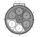
- FIG. 4 In the embodiment shown in FIG. 4, six substrates to be processed 4 are mounted on the rotating susceptor 3.
- the fan-shaped metal-containing reactive gas supply / exhaust unit 21 and the non-metal reactive gas supply / exhaust unit 22 occupy an area corresponding to two substrates each at the same opening angle, and each of them corresponds to one substrate. Just placed apart.
- the purge gas supply / exhaust unit 23 is disposed in a gas separation region having a width corresponding to the one substrate.
- the metal-containing reactive gas supply / exhaust unit 21 and the non-metal reactive gas supply / exhaust unit 22 are not located on the same substrate at any timing, the recess 32 of the rotating susceptor 3 and the substrate 4 in FIG. Mixing of the reaction gas that has passed through the gap between the two does not occur, and backside particles do not increase.
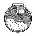
- FIG. 10 shows another embodiment of the third aspect of the present invention.
- the larger the area of the reactive gas supply / exhaust parts 21 and 22 is the longer the contact time between the substrate 4 to be processed and the reactive gas is, and the faster the rotation can be, thereby improving the throughput. be able to.
- it is effective to maintain the contact time between the nonmetal reaction gas and the substrate 4 to be processed as long as possible.
- the metal-containing reaction gas supply / exhaust unit 21 occupies an area corresponding to one substrate, while the non-metal supply unit 22 has an area corresponding to three substrates. It is a case of occupying.
- FIG. 10 shows another embodiment of the third aspect of the present invention.
- FIG. 11 shows another embodiment of the third invention.
- the metal-containing reactive gas supply / exhaust unit 21 occupies an area corresponding to 1.5 substrates, while the non-metal reactive gas supply / exhaust unit 22 has 2.5 sheets. In this case, an area corresponding to the substrate is occupied. In this case, the boundary between each gas supply unit and the location of the substrate to be processed are shifted, but the metal-containing reaction gas supply / exhaust unit 21 and the nonmetal reaction gas supply / exhaust unit 22 are equivalent to one substrate at all times.
- the area of the metal-containing reaction gas supply / exhaust unit 21 may be larger than the area of the non-metal reaction gas supply / exhaust unit 22, and any reaction gas supply / exhaust unit Whether to take a structure is determined in accordance with the ratio of the minimum exposure time required for the metal-containing reactive gas adsorption reaction required to maintain the ALD saturation reaction and the minimum required exposure time for the nonmetal gas reactive gas adsorption reaction. In any case, it is important that the metal-containing reaction gas supply / exhaust unit 21 and the non-metal gas reaction supply / exhaust unit 22 are installed at a distance of a fan-shaped area corresponding to one substrate.
- FIGS. 12 to 17 The embodiment of the present invention disclosed in FIGS. 12 to 17 is a case where eight substrates to be processed 4 are mounted on the rotating susceptor 3, and different metal-containing reaction gas supply / exhaust sections 21 and nonmetal reaction gas supply / exhaust.
- the structure form of area ratio with the part 22 is shown.
- information other than information on the relative position between the substrate and the gas supply means such as a film thickness meter, a gap measuring device, and a substrate lifting pin, is omitted.
- the metal-containing reactive gas supply / exhaust unit 21 and the non-metal reactive gas supply / exhaust unit 22 have the same area, and each cover an area corresponding to three substrates.
- both the reactive gas supply / exhaust portions are arranged apart from each other by an area corresponding to one substrate, mixing of both gases through the gap around the substrate 4 does not occur.
- the area ratio of the area covered by the metal-containing reaction gas supply / exhaust unit 21 and the nonmetal reaction gas supply / exhaust unit 22 is 2.5: 3.5, It is an embodiment of the present invention in the case of 2: 4, 1.5: 4.5, 1: 5 mm.
- the metal-containing reaction gas supply / exhaust unit 21 and the non-metal reaction gas supply / exhaust unit 22 are separated from each other by one substrate, and the reaction gas that has propagated through the gaps around the substrate 4 Mixing does not occur.
- the area ratio of the metal-containing reaction gas supply / exhaust unit 21 and the nonmetal reaction gas supply / exhaust unit 22 is not limited to these values. Any ratio is acceptable as long as it is between 1: 5.
- the area of the metal-containing reaction gas supply / exhaust unit 21 may be larger than the area of the non-metal reaction gas supply / exhaust unit 22, and what kind of reaction gas supply / exhaust unit structure is adopted depends on ALD saturation. It is determined according to the ratio of the minimum required exposure time of the metal-containing reactive gas adsorption reaction required to maintain the reaction and the minimum required exposure time of the nonmetal gas reactive gas adsorption reaction. In any case, it is important that the metal-containing reaction gas supply / exhaust unit 21 and the non-metal gas reaction supply / exhaust unit 22 are installed at a distance of a fan-shaped area corresponding to one substrate.
- FIG. 17 shows another embodiment of the ALD apparatus in which eight substrates to be processed are mounted on the third invention.
- two sets of the metal-containing reactive gas supply / exhaust unit 21 and the non-metal reactive gas supply / exhaust unit 22 are arranged with an area corresponding to one substrate, respectively.
- This embodiment has an advantage that a hybrid film composed of films of different components can be deposited by supplying two kinds of metal-containing reaction gases and / or two kinds of nonmetal reaction gases.
- a HfO / AlO hybrid film is formed by supplying a first metal-containing reaction gas as an Hf precursor gas, a second metal-containing reaction gas as an Al precursor gas, and ozone from two nonmetal reaction gas supply units.
- each reaction gas supply / exhaust unit occupies only an area corresponding to one substrate, so that the time for which the substrate to be processed contacts the reaction gas in each reaction gas supply unit is shortened. Accordingly, the rotational speed of the rotating susceptor is decreased, and the throughput is decreased.
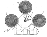
- the upper gas supply means 2 is a mechanism that can change its position in the vertical direction via the flexible bellows 29 with respect to the vacuum vessel 1. It is supported. That is, the upper permanent magnet and the lower permanent magnet are installed so as to repel each other, and the upper gas supply means 2 is held floating. As shown in FIG. 19, a large number of permanent magnet pairs 30 are installed around the vacuum vessel 1 at a certain interval so that the load is evenly distributed, but are installed so as to occupy the entire outer periphery of the vacuum vessel. May be.
- the strength and configuration of the magnet are selected so that a balance is obtained immediately before the upper gas supply means 2 floats in a state where the vacuum vessel is evacuated and has a differential pressure with respect to the atmospheric pressure.
- a permanent magnet pair is used as a floating holding device for the upper gas supply / exhaust means 2, but a spring, an electromagnetic coil, or the like may be used. It is important to use in combination with means.
- the purge gas is ejected from the peripheral purge gas supply unit 25 and / or the central purge gas supply / exhaust unit 24 toward the rotating susceptor 3 at a pressure of 1 Torr number Torr that is the same as or slightly higher than that of the ALD process.
- the metal-containing reaction gas, the non-metal reaction gas, and the purge gas supplied between them also have a floating force corresponding to the differential pressure between the process pressure and the vacuum vessel base pressure, and these gas supply means can also be used as an air cushion. good. Considering all of these, the air cushion force is about 20 kg in this example.
- This floating force is not large enough to lift the upper gas supply / exhaust means, but is sufficiently large when combined with the aforementioned floating holding means such as a spring or magnet.
- gas ejection holes and exhaust holes may be alternately arranged on the shower plate. In this case, the repulsive force and the attractive force act simultaneously, and the gap can be controlled in a self-aligning manner with higher accuracy.
- the gap g is measured by the laser light measuring means 16 to control the gap.
- the gap is controlled by PID feedback to the purge gas ejection amount adjusting valve 20 via the sequencer 17.
- the laser beam measuring means 16 is measured at three different points, and the gas supply amount from the purge gas supply unit divided into three in the circumferential direction is individually controlled, so that the in-plane uniformity of the entire susceptor region of the gap is achieved. Improved the performance.
- the number of divisions in the circumferential direction of the gas supply unit may be further increased to improve uniform gap control characteristics.
- the number of the laser optical measuring means 16 may be selected so as to be economically optimal by comparing the reduction of gas usage by gap control and the device manufacturing cost.
- this gap control is incorporated into an ALD film formation control system, and the substrate to be processed 4 is mounted on the susceptor 3 in the vacuum vessel and evacuated to vacuum, and then the ALD process is completed and rotated. Is stopped at all times until it is evacuated to high vacuum and immediately before the gate valve is opened.
- the gap g between the lower end of the upper gas supply / exhaust means 2 and the rotary susceptor 3 is maintained at a distance of about 1 millimeter or less. We were able to.
- FIG. 5 Regarding the film forming process sequence, first, in FIG. 5, the exhaust port 26 provided in the lower part 6 of the vacuum vessel 1 and the exhaust ports 215, 225, 235 of the gas supply / exhaust means 2 disposed on the upper part of the vacuum vessel 1.
- the vacuum pump 63, 216, and 226 are used to evacuate the vacuum vessel 1 and the entire inside of the gas supply / exhaust means 2 to high vacuum.
- the gate valve 5 provided in the vacuum vessel 1 is opened, and the arm 8 that can be driven up and down is driven to raise the pin 7, and using a vacuum transfer robot (not shown),
- the substrate 4 to be processed is transported to the position of the recess 32 of the rotating susceptor 3 set to a predetermined temperature in advance, and the substrate 4 to be processed is mounted on the pins 7.
- the pin holding arm 8 is driven through the magnetic shield 9 to lower the pin 7 downward, and the substrate 4 to be processed is mounted in the recess 32 of the rotating susceptor 3.
- the rotating susceptor 3 After the first substrate is mounted on the rotating susceptor 3, the rotating susceptor 3 is rotated counterclockwise to the next substrate mounting position, and the second substrate to be processed 4 is mounted on the rotating susceptor 3 in the same manner. . By repeating this, all the substrates to be processed 4 are mounted on the rotating susceptor 3. After all the substrates to be processed are mounted, the substrate to be processed 4 is brought into close contact with the susceptor 3 by an electrostatic chuck (not shown) embedded in the rotating susceptor 3 and the gate valve 5 is closed.
- the number of substrates to be processed the target film thickness, the rotational susceptor home position, the single ALD cycle deposition rate, the maximum aspect ratio of the pattern formed on the substrate to be processed, etc.
- the purge gas is supplied from the purge gas supply unit 23 at the upper part of the vacuum vessel, the central purge gas supply unit 24, and the peripheral purge gas supply unit 25 installed around the vacuum vessel 6, and is evacuated from each gas exhaust groove.
- the pressure is set so that the inside of the vacuum container has a predetermined process pressure.
- rotation of the rotating susceptor 3 is started at the initial rotation speed, and when the substrate to be processed 4 reaches a predetermined place inputted in advance, the gas supply cutoff valves 39 and 40 are turned on via the gas supply cutoff sequencer 38.
- the metal-containing reaction gas and / or the non-metal reaction gas is ejected from the respective reaction gas supply / exhaust units 21 and 22 and exhaust is started.
- a purge gas may be flowed in advance from each reaction gas supply unit, and the reaction gas may be switched to a predetermined position.
- the first rotation is performed with a variable rotation speed pattern at the start of ALD according to the number of substrates to be processed and the configuration of the gas supply / exhaust means 2.
- the rotating susceptor 3 is rotated at the steady ALD rotation speed calculated from the aspect ratio.
- the substrate 4 to be processed is rotated with the rotating susceptor 3 to be sequentially exposed to the metal-containing reaction gas, the purge gas, the nonmetal reaction gas, and the purge gas, and the ALD process proceeds.
- the gas supply is cut off at the pre-input substrate position.
- the gas supply shutoff valves 39 and 40 via the sequencer 38, the supply of the metal-containing reaction gas and the nonmetal reaction gas is shut off to complete the ALD reaction.
- the film thickness is measured in real time by the film thickness meter 14 provided in-line during ALD film formation, the ALD process is completed when the film thickness reaches a predetermined film thickness. By controlling ALD start and completion time, the same film thickness can be obtained for all the substrates to be processed.
- the metal-containing reaction gas and the nonmetal reaction gas are each switched to the purge gas at a predetermined position.
- the rotary susceptor 3 is stopped at the home position, and is lowered downward by the stepping motor to stop the purge gas.
- the gate valve 5 is opened, and the vertical drive pins 7 and a vacuum transfer robot (not shown) are used in the reverse procedure to that when the substrate 4 is mounted on the susceptor 3. Then, the substrate 4 to be processed is discharged from the vacuum vessel 1 to a load lock chamber (not shown).
- the present invention adjusts the number of rotations and the substrate position at the gas supply / stop timing according to the configuration of the gas supply / exhaust means 2 so that the same number of ALD cycles is the same for all the substrates.
- the ALD film having a target film thickness is formed, and the present invention is not limited to the disclosed specific example.
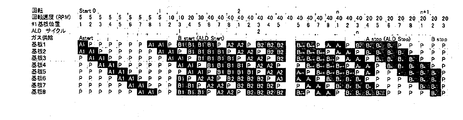
- the number of substrates to be processed is eight, and the metal-containing reaction gas supply / exhaust unit 21 and the nonmetal reaction gas supply / exhaust unit 22 have a purge area corresponding to one substrate to be processed.
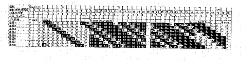
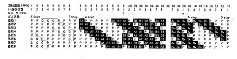
- FIG. 21 shows an ALD process sequence in which both reactive gas supply unit areas occupy an area corresponding to four substrates, and the substrate position at the start and completion of ALD in that sequence. Is shown in FIG. 22 and FIG. In this sequence diagram, symbol A represents a metal-containing reaction gas, symbol B represents a nonmetal reaction gas, and symbol P represents a purge gas.
- the gas supply / exhaust means 2 is divided into eight areas, each numbered 1-8.
- the first substrate corresponds to the first position
- the second substrate corresponds to the eighth position
- the third substrate corresponds to the seventh position in reverse order.
- the metal-containing reaction gas and the nonmetal gas begin to flow at the same time, and that time is set as the ALD start time.
- the first to third substrates are in contact with the metal-containing reaction gas
- the fifth to seventh substrates are in contact with the nonmetal reaction gas.
- the fourth and eighth substrates are in contact with the purge gas.
- the first substrate to be processed is in contact with only one metal reactive gas area, which is 1/3 of the contact time in the steady state.
- the time for which the second substrate to be processed is in contact with the metal reactive gas is 2/3 of the contact time in the steady state.
- the rotation speed is set to 1/3 of steady rotation or less in the first substrate exposure step.
- the rotation speed is set to 2/3 of steady rotation or less.
- the steady rotational speed was 30 RPM
- the rotational speed during processing of the first substrate was 5 RPM
- the rotational speed during processing of the second substrate was 20 RPM.
- the reason why the rotational speed at the start of ALD is set to 5 RPM instead of 10 RPM which is 1/3 of steady rotation is that it may take about 2 seconds or more at the time of switching at the start of reaction gas supply. This is because the time lag until switching is actually ejected to the substrate to be processed is taken into consideration.
- the rotation of the susceptor may be started after the supply of the reaction gas is started and left for about 2 to 3 seconds. By controlling the rotational speed at the start of such ALD, the exposure to the first metal reaction gas can be made sufficiently long for all the substrates to be processed.
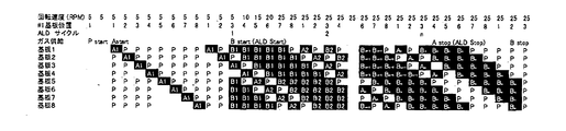
- the ALD stop is the timing at which the metal reactive gas is shut off as shown in FIG.
- the first substrate to be processed is located in the sixth gas supply means area (purge gas supply unit).
- the metal reaction gas is exposed n times to all eight substrates. Even after the metal-containing reaction gas is shut off, the non-metal reaction gas is allowed to flow, and when the first substrate reaches the fourth gas supply means area position at the (n + 1) th rotation, or after that, all the substrates are stopped.
- the surface of the substrate to be processed can be terminated with a non-metal gas.
- the n-layer ALD sequence is applied to all the eight substrates to be processed.
- the eighth substrate to be processed has just entered the area of the last metal-containing reaction gas supply means, and the metal-containing reaction gas is only one-third of the time in the steady rotation state. There is no contact. Therefore, in the final substrate processing step at the completion of ALD, the susceptor rotation speed is set to 1/3 of the steady speed or lower.
- the contact time of the seventh substrate to be processed with the metal-containing reaction gas is 2/3 of the steady rotation state, so that the rotation speed is the steady rotation speed. 2/3 or less. In this example, the rotational speed was reduced to 20 RPM at the time two sheets before the metal-containing reaction gas was shut off, and further, the rotational speed was reduced to 10 RPM when shut off.
- the steady rotation speed is set to 30 rotations per minute, but it is not fixed to this value. As will be described later in the sixth embodiment of the present invention, it depends on the maximum aspect ratio of the substrate pattern to be processed. Can be set in advance. For example, if the pattern has an aspect ratio of about 10, the rotational speed can be increased to about 200 RPM without deteriorating the step coverage characteristic. In addition, when performing variable rotation speed control at the start and completion of ALD, the time required for the first and last rotations is somewhat longer, but the overall rotation speed is 100 rotations or more. Small enough to be ignored.
- the number of substrates to be processed is eight, and the purge area corresponding to one substrate to be processed includes the metal-containing reaction gas supply / exhaust unit 21 and the nonmetal reaction gas supply / exhaust unit 22.
- FIG. 24 shows an ALD process sequence for another embodiment in which both reaction gas supply unit areas cover the same area corresponding to four substrates, respectively, and the ALD in that sequence is arranged. The substrate positions at the start and completion are shown in FIGS. In the ALD process, a so-called incubation occurs in which the adsorption reaction hardly proceeds and film formation does not proceed for the first few cycles.
- the first metal reactive gas adsorption is difficult to proceed, and it is necessary to contact only the metal-containing reactive gas with the substrate to be processed for a relatively long time.
- the first layer atoms adsorbed on the substrate to be processed are either metal atoms or nonmetal atoms, the characteristics of the thin film formed by ALD may deteriorate. Therefore, in this example, assuming that the first layer of adsorbed atoms is metal, the initial adsorption reaction of metal atoms is sufficiently promoted by flowing only the metal-containing reaction gas for the first several rotations, and then When the processing substrate 4 arrives at a predetermined gas supply / exhaust means 2, a non-metal reactive gas was flowed.
- the time when the nonmetal reaction gas starts to flow is defined as the ALD start time.
- the first substrate to be processed has reached the third position (first non-metal reactive gas supply unit).
- the seventh substrate since the seventh substrate is in the fifth position, it is exposed only to one non-metal reactive gas supply / exhaust unit 22 and is normally exposed to three consecutive non-metallic reactive gas / exhaust units 22.
- the contact time is 1/3 compared to the state.
- the time for the eighth substrate to contact the non-metal reactive gas is 2/3 of the steady state.
- the rotation speed is set to 1/3 or less of the steady rotation when processing the first substrate, and the steady rotation speed when processing the second substrate. 2/3, or less than that.
- the time during which only the metal-containing reaction gas is supplied is one cycle. However, if the incubation time is long, this cycle may be further increased to several cycles.
- the ALD stop is the timing at which the metal reactive gas is shut off as in the previous embodiment.
- the first substrate to be processed is located in the fourth gas supply means area (the center of the nonmetal reaction gas supply section).
- the metal reaction gas is exposed n times to all eight substrates. Even after the metal-containing reaction gas is shut off, the non-metal reaction gas continues to flow, and when the first substrate reaches the second gas supply means area position at the (n + 1) th rotation, or stops after that, all substrates are stopped.
- the surface of the substrate to be processed can be terminated with a non-metal gas.
- the n-layer ALD sequence is applied to all the eight substrates to be processed.
- the sixth substrate to be processed has just entered the area of the last metal-containing reaction gas supply means, and the metal-containing reaction gas is only one-third of the time in the steady rotation state. There is no contact. Therefore, in the final substrate processing step at the completion of ALD, the susceptor rotation speed is set to 1/3 of the steady speed or lower.
- the contact time of the fifth substrate to be processed with the metal-containing reaction gas is 2/3 of the steady rotation state, so that the rotation speed is the steady rotation speed. 2/3 or less. In this example, the rotational speed was reduced to 20 RPM at the time two sheets before the metal-containing reaction gas was shut off, and further, the rotational speed was reduced to 10 RPM when shut off.
- the metal-containing reaction supply / exhaust unit 21 and the nonmetal reaction gas supply: exhaust unit 22 are arranged across an area corresponding to one substrate to be processed, the nonmetal reaction gas supply / exhaust unit 22 contains metal.
- the metal-containing reaction gas is sufficiently adsorbed on the substrate surface by flowing only the metal-containing reaction gas during the first rotation, and then the first substrate to be processed in the second rotation.
- the gas reached the third position, the non-metal reactive gas began to flow, and this time was defined as the ALD start time.
- the cycle of flowing only the metal-containing gas may be further extended.
- the areas that first contact the non-metal gas are 1/4, 1/2, and 3/4, respectively, compared to the steady state.
- the rotation speeds during the first, second, and third substrate processing are set to 1/4, 1/2, 3/4 of the steady rotation speed, or less than these rotation speeds, respectively.
- the contact time with the nonmetal can be made the same for all the substrates.
- the completion of ALD the supply of the metal-containing reaction gas is stopped when the first substrate reaches the fourth position at the n-th rotation, and this time is defined as the completion of ALD.
- the rotation speed during the last substrate processing is 1 ⁇ 2 of the steady rotation speed, or The number of rotations was less than that, so that all the substrates could ensure the same contact time for the nth nonmetal gas.
- only the non-metal reactive gas was allowed to flow so that all the substrates to be processed were blacked during ALD of the n layer and their surfaces were terminated with non-metal.
- the metal-containing reaction gas supply / exhaust unit 21 occupies an area corresponding to one substrate
- the nonmetal reaction gas supply / exhaust unit 22 occupies an area corresponding to five substrates.
- the substrate position control at the start and completion of ALD is performed according to the ALD sequence shown in FIG.
- the n-layer ALD process can be performed on all the substrates to be processed, the same exposure time can be maintained, and all the surfaces can be terminated with a non-metal gas.
- the detailed description is the same as that in the above embodiment, and is omitted because it overlaps.
- the number of substrates to be processed is eight, and the metal-containing reaction gas supply / exhaust unit 21 and the nonmetal reaction gas supply / exhaust unit 22 supply purge gas equivalent to one substrate to be processed.
- the metal-containing reaction gas supply / exhaust unit 21 and the non-metal reaction gas supply / exhaust unit 22 occupy an area corresponding to 2.5 and 3.5 substrates, respectively.
- FIG. 31 in order to reduce the incubation, only the metal-containing reaction gas is flowed to ensure that the metal-containing reaction gas is sufficiently adsorbed on the substrate surface.
- the non-metal reactive gas starts to flow, and this time is defined as the ALD start time.
- the areas that first contact the non-metal gas are 2/7, 4/7, and 6/7, respectively, compared to the steady state.
- the rotation speeds during the first, second, and third substrate processings are 2/7, 4/7, and 6/7 of the steady rotation speed, or less than these rotation speeds, respectively.
- the RPM is set to 5 RPM.
- ALD completion As shown in FIG. 33, when the first substrate reaches the third and fourth intermediate positions at the n-th rotation, the point of time when the metal-containing reaction gas is stopped is regarded as ALD completion. At this time, since the fifth and fourth substrates are in contact with the metal reaction gas only in an area of 2/5 and 4/5, respectively, with respect to the steady state, The number of revolutions is 4/5, 2/5, or less than the regular number of revolutions, so that all the substrates can ensure the same contact time for the nth non-metal gas.
- the non-metal reactive gas is allowed to flow so that all the substrates to be processed are subjected to n-layer ALD film formation, and the same exposure time is maintained, and their surfaces are terminated with the non-metal gas. be able to.
- the number of substrates to be processed is eight, and the metal-containing reaction gas supply / exhaust unit 21 and the nonmetal reaction gas supply / exhaust unit 22 are supplied with purge gas corresponding to one substrate to be processed / exhaust.
- the metal-containing reaction gas supply / exhaust unit 21 and the nonmetal reaction gas supply / exhaust unit 22 occupy an area corresponding to 1.5 and 4.5 substrates, respectively.
- An example of the ALD process sequence is shown in FIG. In this case as well, by performing substrate position control and variable rotation speed control at the start and completion of ALD, nLD layer ALD processing is performed for all substrates to be processed, and the same exposure time is maintained. All these surfaces can be terminated with a non-metal gas.
- the detailed description is the same as that in the above embodiment, and is omitted because it overlaps.
- FIGS. 35 to 37 show examples of implementation ALD sequences when one rotation of the rotating susceptor 3 is composed of a plurality of ALD cycles.
- symbols A, B, C, D, and P represent a first metal-containing reaction gas, a first nonmetal reaction gas, a second metal-containing reaction gas, a second nonmetal reaction gas, and a purge gas, respectively.
- FIG. 17 eight substrates to be processed are mounted on the rotating susceptor 3, and one gas supply / exhaust gas composed of a metal-containing reaction gas, a first purge gas, a nonmetal reaction gas, and a second purge gas is provided. Two sets of means are arranged. In this case, as shown in FIG.
- the rotation speed at the start and the normal rotation speed are set to 1/3.
- the film containing the first metal is first deposited on the substrate
- the film containing the second metal is first deposited on the substrate.
- both the first and second metal-containing reaction gases are shut off when the first substrate immediately after reaching n + 1 rotation reaches the first position, and this time is set as the ALD completion time.
- the first and second non-metal reactive gases are shut off when the first substrate reaches the third position or later.
- ALD films deposited for a predetermined number of times on all the substrates are obtained, and all the substrate surfaces are terminated with a non-metal reactive gas and are in a stable state.
- the outermost surface layer is composed of a film containing the second metal, but the outermost surface layers of the fourth to eighth substrates are composed of a film containing the first metal. Is done.
- FIG. 36 shows an ALD process sequence in the case of starting the film formation from the film containing the first metal for all the substrates in the configuration of the gas supply / exhaust means shown in FIG.
- the rotation susceptor 3 when the rotation susceptor 3 is at the home position, the supply of the first metal-containing reaction gas and the first nonmetal reaction gas is started and the rotation is started.
- the first substrate reaches the fifth position, the supply of the second metal-containing reaction gas and the second nonmetal reaction gas is started.
- a film containing the first metal is first formed on all the substrates, and then a film containing the second metal is formed.
- FIG. 37 shows an example in which all the substrates are formed with a film containing only the first metal in the configuration of the gas supply / exhaust means shown in FIG.
- the supply of two non-metal reactive gases is started, and this time is set as the ALD start time.
- ALD completion when the first substrate reaches the third position at the n-th rotation, the two metal-containing reaction gas supply / exhaust parts are shut off, and then the first substrate reaches the sixth position. Sometimes shut off both non-metal reactive gases.
- 2n layer (even number) ALD film formation is performed on all the substrates.
- the metal reactive gas supply / exhaust unit 21 and the non-metal gas supply / exhaust unit 22 both occupy an area corresponding to two substrates, and each corresponds to a single substrate.
- the purge gas supply / exhaust portion 23 is disposed with a space therebetween.
- first, only the metal-containing reaction gas is allowed to flow so that the metal-containing reaction gas is sufficiently adsorbed on the surfaces of all the substrates to be processed.
- the first substrate is the third substrate.
- the supply of the nonmetal reactive gas is started, and this time is set as the ALD start time of the first layer.
- the nth rotation is reached, and when the first substrate reaches the fourth position as shown in FIG. 40, the supply of the metal-containing reaction gas is stopped, and thereafter, only the nonmetal gas is supplied.
- n-layer ALD film formation can be performed on all six substrates, and the surfaces of all the substrates can be terminated with a stable non-metal gas.
- all substrates to be processed have the same reaction in the first layer and the last n layer starting ALD by controlling the variable rotation to reduce the rotation speed. Gas contact time can be secured.
- the metal-containing reactive gas supply / exhaust unit 21 is one substrate
- the non-metal reactive gas supply / exhaust unit 22 is three substrates.
- One ALD process sequence is shown in FIG. 41 for the configuration that occupies the corresponding areas and is separated by the purge gas supply / exhaust unit 23 that occupies the area corresponding to one substrate. In this embodiment, all the gas supply is started at the home position where the first substrate is at the first position, and this time is set as the ALD start time.
- the metal-containing reaction gas is cut off when the first substrate reaches the first position, and this time is set as the ALD completion time.
- the first substrate stops at the 5th position or after that at the (n + 1) th rotation.
- n-layer ALD film formation can be performed on all six substrates, and the surfaces of all the substrates can be terminated with a stable non-metal reactive gas.
- the first layer at the start of ALD takes into account the time lag for switching from purge gas to non-metal reactive gas, and by reducing the number of rotations, The substrate ensures the same reactive gas processing contact time. In this embodiment, variable rotation control at the time of completion is not required.
- FIG. 11 shows six substrates to be processed.
- the metal-containing reaction gas supply / exhaust unit 21 is 1.5 substrates
- the nonmetal reaction gas supply / exhaust unit 22 shows one ALD process sequence for the configuration in which each occupies an area corresponding to 2.5 substrates and separated by the purge gas supply / exhaust unit 23 occupying an area corresponding to one substrate. Shown in In this embodiment, as shown in FIG. 43B, the supply of the metal-containing reaction gas is started when the first substrate reaches the second and third intermediate positions, and this time is set as the ALD start time.
- n-layer ALD film formation can be performed on all six substrates, and the surfaces of all the substrates can be terminated with a stable non-metal gas.
- the number of substrates to be processed is eight, all the substrates to be processed are identical in the first layer and the last n-th layer starting ALD by performing variable rotation control that reduces the number of rotations. The reaction gas treatment contact time is ensured.
- a thin film such as a TiN metal electrode or a high-k insulating film of a DRAM capacitor is formed by ALD
- a natural oxide film formed on the surface of the substrate to be processed is removed, or conversely, the substrate surface is increased by low damage plasma.
- Substrate pretreatment to form a quality radical oxide film may be required.
- the pretreatment process is performed using a pretreatment chamber different from the ALD chamber.
- the device configuration is a cluster system, which is expensive and reduces productivity.
- a substrate to be processed is pretreated with an etching gas (gas C) before performing ALD film formation.
- gas C etching gas
- the etching time and the overetch rate are set, and the number of rotations necessary for the pretreatment is calculated.
- the etching gas is jetted from the two reaction gas supply / exhaust portions 21 and 22 to the surface of the substrate to be processed, and the surface is etched.
- the susceptor is rotated in order to maintain the etching uniformity for all the substrates.
- the rotational speed does not affect the productivity, it may be slow.
- the gas is switched to the purge gas and the rotation is continued for 2 to 3 revolutions.
- the supply of the metal-containing reaction gas is started, and the metal-containing reaction gas is adsorbed on the sufficiently surface-treated substrate surface.
- the second substrate reaches the first position (home position)
- the supply of the nonmetal reactive gas is started, and this time is set as the ALD start time.
- the ALD stop when the first substrate reaches the second position at the nth rotation, the supply of the metal-containing reaction gas is stopped, and this time is set as the ALD completion time.
- the nonmetal continues to flow after that, and the supply of the nonmetal reactive gas is stopped when the first substrate reaches the eighth position at the n-th rotation or thereafter.
- FIG. 46 illustrates another embodiment of the pretreatment process.
- oxygen radicals, nitrogen radicals, and hydrogen radicals are generated using excitation means such as plasma installed in the non-metal reactive gas supply unit 221 to form high-quality radical oxide films and radical nitride films on the substrate to be processed.
- excitation means such as plasma installed in the non-metal reactive gas supply unit 221 to form high-quality radical oxide films and radical nitride films on the substrate to be processed.
- a high quality ALD thin film is formed by an ALD process.
- the sixth aspect of the present invention will be described using the rotation speed control sequence shown in FIG. First, when the ALD saturation reaction time for the maximum aspect ratio pattern of the substrate to be processed is already known, the value is input to the apparatus process recipe. When it is unknown, the process pressure, temperature, reaction gas species, and maximum aspect ratio are input, and the saturation reaction time corresponding function for the maximum aspect ratio pattern under these process conditions is calculated. As one example of the function calculation, when performing ALD film formation on a pattern having an aspect ratio of 10 or more, a saturation time t s1 at a certain aspect ratio ⁇ 1 is obtained at a certain process pressure P 1 and a certain temperature T 1 . describes any temperature T, pressure P, and the saturation time t s in the aspect ratio ⁇ by the following equation.
- a case where the rotational speed is gradually changed according to the film thickness during the ALD process is disclosed. That is, if the initial aspect ratio before the ALD process is ⁇ 0 and the film thickness formed in a single ALD cycle is h, a film having a thickness of h is formed on both side walls in the nth cycle.
- d is the width or diameter of the maximum aspect ratio pattern.
- the saturation time of the nth cycle is obtained from this ⁇ (n), the rotation speed at that time is calculated, and the rotation speed is changed in real time.
- FIG. 48 and 49 show an apparatus system equipped with a plurality of ALD process chambers of the present invention.
- the four-chamber ALD film forming system 42 shown in FIG. 48 six substrates are mounted in one ALD process chamber 43, and four process chambers are mounted in one system. Therefore, 24 substrates can be formed simultaneously.
- the three-chamber ALD film forming system 44 shown in FIG. 49 eight substrates are mounted in one ALD process chamber 45, and three process chambers are mounted in one system. Both systems have a common end station 49, load / unload load chamber 48, vacuum transfer chamber 47, and substrate vacuum transfer robot 46, and one system has the ability to process 24 sheets simultaneously as one lot.
- the number of process chambers and the number of substrates are not limited to those in the present embodiment, and an appropriate system may be selected according to the production volume and production type.
- a process embodiment in which the apparatus and process of the present invention are applied to TiN ALD film formation using the four-chamber configuration system shown in FIG. 48 will be described.
- a TiN film of 10 nm was formed using TiCl 4 and NH 3 as a metal reaction gas and a nonmetal reaction gas, respectively, using the rotating semi-batch ALD apparatus of the present invention.
- the substrate to be processed a silicon substrate in which holes having a diameter of 50 nm and an aspect ratio of 80 were patterned was used. Nitrogen was used as the purge gas.
- six substrates to be processed having a diameter of 300 mm are mounted on the rotating susceptor.
- the metal-containing reaction gas supply unit and the nonmetal reaction gas supply unit each cover an area corresponding to two substrates and correspond to one substrate. It is separated by a purge gas supply that occupies the area.
- a central purge gas supply unit is installed at a radius of 12 cm at the center of the vacuum vessel. Further, a peripheral purge gas supply unit having a width of 7 cm was also arranged in the peripheral part.
- the metal-containing reaction gas supply unit, the nonmetal reaction gas supply unit, and the purge gas supply unit were all surrounded by a vacuum exhaust groove having a width of 2 cm.
- the gas flow rates of TiCl 4 and NH 3 were each 200 SCCM.
- the purge gas flow rate is 400 SCCM each. All the vacuum vessel walls were heated to 200 ° C.
- the gas supply means was held by a flange and 24 springs as shown in FIG.
- the setting gap was 0.8 mm, and the gap between the gas supply means and the substrate to be processed was measured at three points on the substrate to be processed by an optical laser beam.
- the substrate By supplying 500 SCCM and 1 SLM respectively from the central purge gas and the peripheral purge gas supply unit, the substrate could be stably held at a gap of 0.8 mm without contacting the gas supply means.
- ALD start / completion timing gas supply start and shut-off were performed according to the sequence of FIG.
- the saturation time at an aspect ratio of 80 was 1.8 seconds, and the initial steady rotational speed was set to 10 RPM.
- the saturation time at the time of completion was about 4.8 seconds, and the rotation speed was 6 RPM.
- the average throughput of one ALD process chamber is 25 WPH, including overheads such as substrate transfer and temperature rise. In the 4-chamber system shown in FIG. 49, the overhead due to the substrate transfer between the end station and the process chamber is reduced. Nevertheless, a high throughput of 80 WPH could be achieved.
- step coverage was observed with a scanning electron microscope and a transmission electron microscope, and as a result, 100% step coverage was obtained even for holes with an aspect ratio of 80.
- the particles 3000 marathon tests were performed, and stable results were obtained with about +5 on the substrate surface side and about +500 on the back surface side.
- the film thickness of TiN was 10.08 nm, and in-plane uniformity and inter-plane reproducibility were 0.8% (3 ⁇ ), and very good performance was achieved.
- the gas utilization efficiency that is, the ratio of Ti and N atoms deposited as TiN in the supplied TiCl 4 and NH 3 gas was 2% for both. This shows that the gas utilization efficiency of ordinary ALD is twice as high as 1% or less, and it can be found that it can contribute to a very large raw material gas cost reduction.
- the present specification mainly describes the application to the semiconductor manufacturing process
- the present invention improves the performance of high productivity, high step coverage, and low gas consumption by changing the size, shape, material, etc. of the substrate.
- an ALD surface treatment device it can be used in a wide range of industries for manufacturing devices such as liquid crystals, solar cells, LEDs, lithium ion secondary battery electrodes, nanomaterials, and biomaterials.
- FIG. 1 is a diagram illustrating a problem in the ALD process, and shows the relationship between the reaction gas exposure time and the reaction rate.
- FIG. 2 is a diagram illustrating the discovery leading to the present invention, and shows the relationship between the reaction gas exposure time and the step coverage.
- FIG. 3 is a diagram for explaining the discovery leading to the present invention, and shows the relationship between the aspect ratio of the pattern etched on the surface of the substrate to be processed and the ALD saturation reaction time.
- FIG. 4 is an explanatory diagram showing an ALD apparatus plane in an embodiment in which six substrates to be processed are mounted, and both the metal-containing reaction gas supply means and the nonmetal reaction gas supply means occupy an area corresponding to two substrates. It is.
- FIG. 1 is a diagram illustrating a problem in the ALD process, and shows the relationship between the reaction gas exposure time and the reaction rate.
- FIG. 2 is a diagram illustrating the discovery leading to the present invention, and shows the relationship between the reaction gas exposure time and the step coverage.
- FIG. 3
- FIG. 5 is an explanatory view showing a cross section of the ALD apparatus along the line ABC in the embodiment of the present invention in FIG.
- FIG. 6 is an explanatory view showing a cross section of the ALD apparatus along the line ABD in the embodiment of the present invention in FIG.
- FIG. 7 is an explanatory view showing a cross section of the metal-containing reaction gas supply unit in the first and second embodiments of the present invention.
- FIG. 8 is an explanatory view showing a cross section of the non-metal reactive gas supply section in the first and second embodiments of the present invention.
- FIG. 9 is an explanatory view showing a cross section of the purge gas supply section in the first and second embodiments of the present invention.
- FIG. 10 shows an embodiment of the third aspect of the present invention, and is an explanatory view showing an ALD apparatus plane when six substrates are mounted and the metal-containing reactive gas supply means occupies an area corresponding to one substrate.
- FIG. 11 shows an embodiment of the third aspect of the present invention, and is an explanatory view showing a plane of an ALD apparatus when six substrates are mounted and the metal-containing reactive gas supply means occupies an area corresponding to 1.5 substrates. is there.
- FIG. 12 shows a third embodiment of the present invention, in which eight substrates are mounted, and the ALD apparatus plane when the metal-containing reaction gas supply means and the nonmetal reaction gas supply means both occupy an area corresponding to three substrates. It is explanatory drawing which showed.
- FIG. 11 shows an embodiment of the third aspect of the present invention, and is an explanatory view showing a plane of an ALD apparatus when six substrates are mounted and the metal-containing reactive gas supply means occupies an area corresponding to 1.5 substrates. is there.
- FIG. 12 shows a third
- FIG. 13 shows an embodiment of the third aspect of the present invention, and is an explanatory view showing an ALD apparatus plane when eight substrates are mounted and the metal-containing reaction gas supply means occupies an area corresponding to 2.5 substrates. is there.
- FIG. 14 is an explanatory view showing an ALD apparatus plane in the case where eight substrates are mounted and the metal-containing reactive gas supply means occupies an area corresponding to two substrates, according to a third embodiment of the present invention.
- FIG. 15 shows an embodiment of the third aspect of the present invention, and is an explanatory view showing an ALD apparatus plane when eight substrates are mounted and the metal-containing reaction gas supply means occupies an area corresponding to 1.5 substrates. is there.
- FIG. 16 shows an embodiment of the third aspect of the present invention, and is an explanatory view showing an ALD apparatus plane when eight substrates are mounted and the metal-containing reaction gas supply means occupies an area corresponding to one substrate.
- FIG. 17 shows an embodiment of the third aspect of the present invention, and is an explanatory view showing an ALD apparatus plane when eight substrates are mounted and two pairs of ALD gas supply / exhaust means are installed.
- FIG. 18 is an explanatory view showing a cross-sectional view of an ALD apparatus according to the fourth embodiment of the present invention.
- FIG. 19 is an explanatory view showing a plan view of an ALD apparatus in the fourth embodiment of the present invention.
- FIG. 20 is an explanation showing an ALD film formation control system comprising a gap control flowchart and a gas supply control flowchart in the fourth and fifth embodiments of the present invention.
- FIG. 21 is an explanatory diagram showing an ALD process sequence in the fifth embodiment of the present invention in the configuration in which the gas supply / exhaust means and eight substrates are mounted as shown in FIG.
- FIG. 22 is an explanatory view showing the substrate arrangement at the start of the ALD process in the fifth embodiment of the present invention in the configuration in which the gas supply / exhaust means and eight substrates are mounted as shown in FIG.
- FIG. 23 is an explanatory view showing the substrate arrangement at the completion of the ALD process in the fifth embodiment of the present invention in the configuration in which the gas supply / exhaust means and eight substrates are mounted as shown in FIG.
- FIG. 24 is an explanatory diagram showing an ALD process sequence in the fifth embodiment of the present invention in which incubation is considered in the configuration of the gas supply / exhaust means and eight substrates mounted in FIG.
- FIG. 25 is an explanatory view showing the substrate arrangement at the start of the ALD process in the fifth embodiment of the present invention considering the incubation in the configuration of the gas supply / exhaust means and eight substrates mounted in FIG.
- FIG. 26 is an explanatory view showing the substrate arrangement at the completion of the ALD process in the fifth embodiment of the present invention considering the incubation in the configuration of the gas supply / exhaust means and eight substrates mounted in FIG.
- FIG. 25 is an explanatory view showing the substrate arrangement at the start of the ALD process in the fifth embodiment of the present invention considering the incubation in the configuration of the gas supply / exhaust means and eight substrates mounted in FIG.
- FIG. 26 is an explanatory view showing the substrate arrangement at the completion of the ALD process in the fifth embodiment of the present invention considering the incubation in the configuration of
- FIG. 27 is an explanatory diagram showing an ALD process sequence in the fifth embodiment of the present invention in the configuration in which the gas supply / exhaust means and eight substrates are mounted as shown in FIG.
- FIG. 28 is an explanatory view showing the substrate arrangement at the start of the ALD process in the fifth embodiment of the present invention in the configuration in which the gas supply / exhaust means and eight substrates are mounted as shown in FIG.
- FIG. 29 is an explanatory view showing the substrate arrangement at the completion of the ALD process in the fifth embodiment of the present invention in the configuration in which the gas supply / exhaust means and eight substrates are mounted as shown in FIG.
- FIG. 28 is an explanatory view showing the substrate arrangement at the start of the ALD process in the fifth embodiment of the present invention in the configuration in which the gas supply / exhaust means and eight substrates are mounted as shown in FIG.
- FIG. 29 is an explanatory view showing the substrate arrangement at the completion of the ALD process in the fifth embodiment of the present invention in the configuration in which the gas supply / exhaust means and eight substrate
- FIG. 30 is an explanatory diagram showing an ALD process sequence in the fifth embodiment of the present invention in the configuration in which the gas supply / exhaust means and eight substrates are mounted as shown in FIG.
- FIG. 31 is an explanatory diagram showing an ALD process sequence in the fifth embodiment of the present invention in the configuration in which the gas supply / exhaust means and eight substrates are mounted as shown in FIG.
- FIG. 32 is an explanatory view showing the substrate arrangement at the start of the ALD process in the fifth embodiment of the present invention in the configuration in which the gas supply / exhaust means and eight substrates are mounted as shown in FIG. FIG.
- FIG. 33 is an explanatory view showing the substrate arrangement at the completion of the ALD process in the fifth embodiment of the present invention in the configuration in which the gas supply / exhaust means and eight substrates are mounted as shown in FIG.
- FIG. 34 is an explanatory diagram showing an ALD process sequence in the fifth embodiment of the present invention in the configuration in which the gas supply / exhaust means and eight substrates are mounted as shown in FIG.
- FIG. 35 is an explanatory diagram showing an ALD process sequence in the fifth embodiment of the present invention in the configuration in which the two pairs of gas supply / exhaust means and eight substrates are mounted as shown in FIG. FIG.
- FIG. 36 is an explanatory diagram showing an ALD process sequence in the fifth embodiment of the present invention in the configuration in which two pairs of gas supply / exhaust means and eight substrates are mounted as shown in FIG.
- FIG. 37 is an explanatory diagram showing an ALD process sequence in the fifth embodiment of the present invention in the configuration in which the two pairs of gas supply / exhaust means and eight substrates are mounted as shown in FIG.
- FIG. 38 is an explanatory diagram showing an ALD process sequence in the fifth embodiment of the present invention in the configuration in which the gas supply / exhaust means and six substrates are mounted as shown in FIG. FIG.
- FIG. 39 is an explanatory view showing the substrate arrangement at the start of the ALD process in the fifth embodiment of the present invention in the configuration in which the gas supply / exhaust means and six substrates are mounted as shown in FIG.
- FIG. 40 is an explanatory view showing the substrate arrangement at the completion of the ALD process in the fifth embodiment of the present invention in the configuration in which the gas supply / exhaust means and six substrates are mounted as shown in FIG.
- FIG. 41 is an explanatory diagram showing an ALD process sequence in the fifth embodiment of the present invention in the configuration in which the gas supply / exhaust means and six substrates are mounted as shown in FIG.
- FIG. 42 is an explanatory diagram showing the configuration of the gas supply / exhaust means shown in FIG.
- FIG. 43 is an explanatory diagram showing the configuration of the gas supply / exhaust means shown in FIG. 11 and the substrate arrangement at the start of the ALD process in the fifth embodiment of the present invention when six substrates are mounted.
- FIG. 44 is an explanatory diagram showing the configuration of the gas supply / exhaust means shown in FIG. 11 and the substrate arrangement upon completion of the ALD process in the fifth embodiment of the present invention when six substrates are mounted.
- FIG. 45 is an explanatory diagram showing a fifth sequence of the present invention when the pretreatment and the ALD process are performed in the same chamber using the configuration of the gas supply / exhaust means shown in FIG. FIG.
- FIG. 46 is an explanatory diagram showing a fifth sequence of the present invention in the case where the pretreatment and the ALD process are performed in the same chamber using the configuration of the gas supply / exhaust means configured as shown in FIG.
- FIG. 47 is an explanatory diagram showing a rotation control sequence in the embodiment of the sixth invention.
- FIG. 48 is an explanatory diagram showing an embodiment of an ALD system mounted with six substrates according to the present invention.
- FIG. 49 is an explanatory view showing an embodiment of an ALD system mounted with 8 substrates according to the present invention.
Landscapes
- Chemical & Material Sciences (AREA)
- General Chemical & Material Sciences (AREA)
- Chemical Kinetics & Catalysis (AREA)
- Engineering & Computer Science (AREA)
- Materials Engineering (AREA)
- Mechanical Engineering (AREA)
- Metallurgy (AREA)
- Organic Chemistry (AREA)
- Chemical Vapour Deposition (AREA)
- Electrodes Of Semiconductors (AREA)
Priority Applications (3)
| Application Number | Priority Date | Filing Date | Title |
|---|---|---|---|
| KR1020157023244A KR101803768B1 (ko) | 2013-04-07 | 2014-04-04 | 회전형 세미 배치 ald 장치 및 프로세스 |
| CN201480011039.1A CN105102675B (zh) | 2013-04-07 | 2014-04-04 | 旋转型半批次原子层沉积装置 |
| US14/831,884 US10480073B2 (en) | 2013-04-07 | 2015-08-21 | Rotating semi-batch ALD device |
Applications Claiming Priority (2)
| Application Number | Priority Date | Filing Date | Title |
|---|---|---|---|
| JP2013080037A JP6134191B2 (ja) | 2013-04-07 | 2013-04-07 | 回転型セミバッチald装置 |
| JP2013-080037 | 2013-04-07 |
Related Child Applications (1)
| Application Number | Title | Priority Date | Filing Date |
|---|---|---|---|
| US14/831,884 Continuation US10480073B2 (en) | 2013-04-07 | 2015-08-21 | Rotating semi-batch ALD device |
Publications (1)
| Publication Number | Publication Date |
|---|---|
| WO2014168096A1 true WO2014168096A1 (ja) | 2014-10-16 |
Family
ID=51689505
Family Applications (1)
| Application Number | Title | Priority Date | Filing Date |
|---|---|---|---|
| PCT/JP2014/060027 Ceased WO2014168096A1 (ja) | 2013-04-07 | 2014-04-04 | 回転型セミバッチald装置およびプロセス |
Country Status (6)
| Country | Link |
|---|---|
| US (1) | US10480073B2 (2) |
| JP (1) | JP6134191B2 (2) |
| KR (1) | KR101803768B1 (2) |
| CN (1) | CN105102675B (2) |
| TW (1) | TWI600789B (2) |
| WO (1) | WO2014168096A1 (2) |
Cited By (6)
| Publication number | Priority date | Publication date | Assignee | Title |
|---|---|---|---|---|
| US20160273105A1 (en) * | 2015-03-17 | 2016-09-22 | Asm Ip Holding B.V. | Atomic layer deposition apparatus |
| US20170032943A1 (en) * | 2015-07-27 | 2017-02-02 | Lam Research Corporation | Time varying segmented pressure control |
| WO2017204622A1 (en) * | 2016-05-27 | 2017-11-30 | Asm Ip Holding B.V. | Apparatus for semiconductor wafer processing |
| US10480073B2 (en) | 2013-04-07 | 2019-11-19 | Shigemi Murakawa | Rotating semi-batch ALD device |
| CN110707021A (zh) * | 2018-07-10 | 2020-01-17 | 台湾积体电路制造股份有限公司 | 半导体设备以及半导体制程方法 |
| JP2023544425A (ja) * | 2020-10-12 | 2023-10-23 | ベネク・オサケユフティオ | 原子層堆積装置 |
Families Citing this family (410)
| Publication number | Priority date | Publication date | Assignee | Title |
|---|---|---|---|---|
| US10378106B2 (en) | 2008-11-14 | 2019-08-13 | Asm Ip Holding B.V. | Method of forming insulation film by modified PEALD |
| US9394608B2 (en) | 2009-04-06 | 2016-07-19 | Asm America, Inc. | Semiconductor processing reactor and components thereof |
| US8802201B2 (en) | 2009-08-14 | 2014-08-12 | Asm America, Inc. | Systems and methods for thin-film deposition of metal oxides using excited nitrogen-oxygen species |
| US9312155B2 (en) | 2011-06-06 | 2016-04-12 | Asm Japan K.K. | High-throughput semiconductor-processing apparatus equipped with multiple dual-chamber modules |
| US10364496B2 (en) | 2011-06-27 | 2019-07-30 | Asm Ip Holding B.V. | Dual section module having shared and unshared mass flow controllers |
| US10854498B2 (en) | 2011-07-15 | 2020-12-01 | Asm Ip Holding B.V. | Wafer-supporting device and method for producing same |
| US20130023129A1 (en) | 2011-07-20 | 2013-01-24 | Asm America, Inc. | Pressure transmitter for a semiconductor processing environment |
| US9017481B1 (en) | 2011-10-28 | 2015-04-28 | Asm America, Inc. | Process feed management for semiconductor substrate processing |
| US9659799B2 (en) | 2012-08-28 | 2017-05-23 | Asm Ip Holding B.V. | Systems and methods for dynamic semiconductor process scheduling |
| US9021985B2 (en) | 2012-09-12 | 2015-05-05 | Asm Ip Holdings B.V. | Process gas management for an inductively-coupled plasma deposition reactor |
| US10714315B2 (en) | 2012-10-12 | 2020-07-14 | Asm Ip Holdings B.V. | Semiconductor reaction chamber showerhead |
| US20160376700A1 (en) | 2013-02-01 | 2016-12-29 | Asm Ip Holding B.V. | System for treatment of deposition reactor |
| US9484191B2 (en) | 2013-03-08 | 2016-11-01 | Asm Ip Holding B.V. | Pulsed remote plasma method and system |
| US9589770B2 (en) | 2013-03-08 | 2017-03-07 | Asm Ip Holding B.V. | Method and systems for in-situ formation of intermediate reactive species |
| US9490149B2 (en) * | 2013-07-03 | 2016-11-08 | Lam Research Corporation | Chemical deposition apparatus having conductance control |
| US9240412B2 (en) | 2013-09-27 | 2016-01-19 | Asm Ip Holding B.V. | Semiconductor structure and device and methods of forming same using selective epitaxial process |
| US10683571B2 (en) | 2014-02-25 | 2020-06-16 | Asm Ip Holding B.V. | Gas supply manifold and method of supplying gases to chamber using same |
| US10167557B2 (en) | 2014-03-18 | 2019-01-01 | Asm Ip Holding B.V. | Gas distribution system, reactor including the system, and methods of using the same |
| US11015245B2 (en) | 2014-03-19 | 2021-05-25 | Asm Ip Holding B.V. | Gas-phase reactor and system having exhaust plenum and components thereof |
| US10858737B2 (en) | 2014-07-28 | 2020-12-08 | Asm Ip Holding B.V. | Showerhead assembly and components thereof |
| US9890456B2 (en) | 2014-08-21 | 2018-02-13 | Asm Ip Holding B.V. | Method and system for in situ formation of gas-phase compounds |
| KR102297567B1 (ko) * | 2014-09-01 | 2021-09-02 | 삼성전자주식회사 | 가스 주입 장치 및 이를 포함하는 박막 증착 장비 |
| US9657845B2 (en) | 2014-10-07 | 2017-05-23 | Asm Ip Holding B.V. | Variable conductance gas distribution apparatus and method |
| US10941490B2 (en) | 2014-10-07 | 2021-03-09 | Asm Ip Holding B.V. | Multiple temperature range susceptor, assembly, reactor and system including the susceptor, and methods of using the same |
| JP6330623B2 (ja) * | 2014-10-31 | 2018-05-30 | 東京エレクトロン株式会社 | 成膜装置、成膜方法及び記憶媒体 |
| KR102263121B1 (ko) | 2014-12-22 | 2021-06-09 | 에이에스엠 아이피 홀딩 비.브이. | 반도체 소자 및 그 제조 방법 |
| US10529542B2 (en) | 2015-03-11 | 2020-01-07 | Asm Ip Holdings B.V. | Cross-flow reactor and method |
| US10276355B2 (en) | 2015-03-12 | 2019-04-30 | Asm Ip Holding B.V. | Multi-zone reactor, system including the reactor, and method of using the same |
| US10458018B2 (en) | 2015-06-26 | 2019-10-29 | Asm Ip Holding B.V. | Structures including metal carbide material, devices including the structures, and methods of forming same |
| US10600673B2 (en) * | 2015-07-07 | 2020-03-24 | Asm Ip Holding B.V. | Magnetic susceptor to baseplate seal |
| US10083836B2 (en) | 2015-07-24 | 2018-09-25 | Asm Ip Holding B.V. | Formation of boron-doped titanium metal films with high work function |
| US10204790B2 (en) | 2015-07-28 | 2019-02-12 | Asm Ip Holding B.V. | Methods for thin film deposition |
| US11421321B2 (en) | 2015-07-28 | 2022-08-23 | Asm Ip Holding B.V. | Apparatuses for thin film deposition |
| US20170088952A1 (en) * | 2015-09-28 | 2017-03-30 | Ultratech, Inc. | High-throughput multichamber atomic layer deposition systems and methods |
| US9960072B2 (en) | 2015-09-29 | 2018-05-01 | Asm Ip Holding B.V. | Variable adjustment for precise matching of multiple chamber cavity housings |
| JP6671911B2 (ja) | 2015-10-02 | 2020-03-25 | 株式会社ニューフレアテクノロジー | 位置ずれ検出装置、気相成長装置および位置ずれ検出方法 |
| US10211308B2 (en) | 2015-10-21 | 2019-02-19 | Asm Ip Holding B.V. | NbMC layers |
| US10322384B2 (en) | 2015-11-09 | 2019-06-18 | Asm Ip Holding B.V. | Counter flow mixer for process chamber |
| JP6569521B2 (ja) * | 2015-12-24 | 2019-09-04 | 東京エレクトロン株式会社 | 成膜装置 |
| US11139308B2 (en) | 2015-12-29 | 2021-10-05 | Asm Ip Holding B.V. | Atomic layer deposition of III-V compounds to form V-NAND devices |
| WO2017131404A1 (ko) * | 2016-01-26 | 2017-08-03 | 주성엔지니어링(주) | 기판처리장치 |
| US10468251B2 (en) | 2016-02-19 | 2019-11-05 | Asm Ip Holding B.V. | Method for forming spacers using silicon nitride film for spacer-defined multiple patterning |
| US10529554B2 (en) | 2016-02-19 | 2020-01-07 | Asm Ip Holding B.V. | Method for forming silicon nitride film selectively on sidewalls or flat surfaces of trenches |
| US10501866B2 (en) | 2016-03-09 | 2019-12-10 | Asm Ip Holding B.V. | Gas distribution apparatus for improved film uniformity in an epitaxial system |
| US10343920B2 (en) | 2016-03-18 | 2019-07-09 | Asm Ip Holding B.V. | Aligned carbon nanotubes |
| US9892913B2 (en) | 2016-03-24 | 2018-02-13 | Asm Ip Holding B.V. | Radial and thickness control via biased multi-port injection settings |
| US10190213B2 (en) | 2016-04-21 | 2019-01-29 | Asm Ip Holding B.V. | Deposition of metal borides |
| US10865475B2 (en) | 2016-04-21 | 2020-12-15 | Asm Ip Holding B.V. | Deposition of metal borides and silicides |
| US10032628B2 (en) | 2016-05-02 | 2018-07-24 | Asm Ip Holding B.V. | Source/drain performance through conformal solid state doping |
| US10367080B2 (en) | 2016-05-02 | 2019-07-30 | Asm Ip Holding B.V. | Method of forming a germanium oxynitride film |
| KR102592471B1 (ko) | 2016-05-17 | 2023-10-20 | 에이에스엠 아이피 홀딩 비.브이. | 금속 배선 형성 방법 및 이를 이용한 반도체 장치의 제조 방법 |
| US11453943B2 (en) | 2016-05-25 | 2022-09-27 | Asm Ip Holding B.V. | Method for forming carbon-containing silicon/metal oxide or nitride film by ALD using silicon precursor and hydrocarbon precursor |
| US10388509B2 (en) | 2016-06-28 | 2019-08-20 | Asm Ip Holding B.V. | Formation of epitaxial layers via dislocation filtering |
| KR102483547B1 (ko) * | 2016-06-30 | 2023-01-02 | 삼성전자주식회사 | 가스 공급 유닛 및 이를 포함하는 박막 증착 장치 |
| US9859151B1 (en) | 2016-07-08 | 2018-01-02 | Asm Ip Holding B.V. | Selective film deposition method to form air gaps |
| US10612137B2 (en) | 2016-07-08 | 2020-04-07 | Asm Ip Holdings B.V. | Organic reactants for atomic layer deposition |
| US10714385B2 (en) | 2016-07-19 | 2020-07-14 | Asm Ip Holding B.V. | Selective deposition of tungsten |
| KR102354490B1 (ko) | 2016-07-27 | 2022-01-21 | 에이에스엠 아이피 홀딩 비.브이. | 기판 처리 방법 |
| US9887082B1 (en) | 2016-07-28 | 2018-02-06 | Asm Ip Holding B.V. | Method and apparatus for filling a gap |
| US9812320B1 (en) | 2016-07-28 | 2017-11-07 | Asm Ip Holding B.V. | Method and apparatus for filling a gap |
| US10395919B2 (en) | 2016-07-28 | 2019-08-27 | Asm Ip Holding B.V. | Method and apparatus for filling a gap |
| KR102532607B1 (ko) | 2016-07-28 | 2023-05-15 | 에이에스엠 아이피 홀딩 비.브이. | 기판 가공 장치 및 그 동작 방법 |
| US10246775B2 (en) * | 2016-08-03 | 2019-04-02 | Tokyo Electron Limited | Film forming apparatus, method of forming film, and storage medium |
| US10410943B2 (en) | 2016-10-13 | 2019-09-10 | Asm Ip Holding B.V. | Method for passivating a surface of a semiconductor and related systems |
| US10643826B2 (en) | 2016-10-26 | 2020-05-05 | Asm Ip Holdings B.V. | Methods for thermally calibrating reaction chambers |
| US11532757B2 (en) | 2016-10-27 | 2022-12-20 | Asm Ip Holding B.V. | Deposition of charge trapping layers |
| US10643904B2 (en) | 2016-11-01 | 2020-05-05 | Asm Ip Holdings B.V. | Methods for forming a semiconductor device and related semiconductor device structures |
| US10229833B2 (en) | 2016-11-01 | 2019-03-12 | Asm Ip Holding B.V. | Methods for forming a transition metal nitride film on a substrate by atomic layer deposition and related semiconductor device structures |
| US10435790B2 (en) | 2016-11-01 | 2019-10-08 | Asm Ip Holding B.V. | Method of subatmospheric plasma-enhanced ALD using capacitively coupled electrodes with narrow gap |
| US10714350B2 (en) | 2016-11-01 | 2020-07-14 | ASM IP Holdings, B.V. | Methods for forming a transition metal niobium nitride film on a substrate by atomic layer deposition and related semiconductor device structures |
| US10134757B2 (en) | 2016-11-07 | 2018-11-20 | Asm Ip Holding B.V. | Method of processing a substrate and a device manufactured by using the method |
| KR102546317B1 (ko) | 2016-11-15 | 2023-06-21 | 에이에스엠 아이피 홀딩 비.브이. | 기체 공급 유닛 및 이를 포함하는 기판 처리 장치 |
| US10340135B2 (en) | 2016-11-28 | 2019-07-02 | Asm Ip Holding B.V. | Method of topologically restricted plasma-enhanced cyclic deposition of silicon or metal nitride |
| KR102762543B1 (ko) | 2016-12-14 | 2025-02-05 | 에이에스엠 아이피 홀딩 비.브이. | 기판 처리 장치 |
| US11447861B2 (en) | 2016-12-15 | 2022-09-20 | Asm Ip Holding B.V. | Sequential infiltration synthesis apparatus and a method of forming a patterned structure |
| US11581186B2 (en) | 2016-12-15 | 2023-02-14 | Asm Ip Holding B.V. | Sequential infiltration synthesis apparatus |
| KR102700194B1 (ko) | 2016-12-19 | 2024-08-28 | 에이에스엠 아이피 홀딩 비.브이. | 기판 처리 장치 |
| US10269558B2 (en) | 2016-12-22 | 2019-04-23 | Asm Ip Holding B.V. | Method of forming a structure on a substrate |
| US10692724B2 (en) * | 2016-12-23 | 2020-06-23 | Lam Research Corporation | Atomic layer etching methods and apparatus |
| US10867788B2 (en) | 2016-12-28 | 2020-12-15 | Asm Ip Holding B.V. | Method of forming a structure on a substrate |
| US11390950B2 (en) | 2017-01-10 | 2022-07-19 | Asm Ip Holding B.V. | Reactor system and method to reduce residue buildup during a film deposition process |
| US10655221B2 (en) | 2017-02-09 | 2020-05-19 | Asm Ip Holding B.V. | Method for depositing oxide film by thermal ALD and PEALD |
| US10468261B2 (en) | 2017-02-15 | 2019-11-05 | Asm Ip Holding B.V. | Methods for forming a metallic film on a substrate by cyclical deposition and related semiconductor device structures |
| US10529563B2 (en) | 2017-03-29 | 2020-01-07 | Asm Ip Holdings B.V. | Method for forming doped metal oxide films on a substrate by cyclical deposition and related semiconductor device structures |
| US10283353B2 (en) | 2017-03-29 | 2019-05-07 | Asm Ip Holding B.V. | Method of reforming insulating film deposited on substrate with recess pattern |
| KR102457289B1 (ko) | 2017-04-25 | 2022-10-21 | 에이에스엠 아이피 홀딩 비.브이. | 박막 증착 방법 및 반도체 장치의 제조 방법 |
| US10892156B2 (en) | 2017-05-08 | 2021-01-12 | Asm Ip Holding B.V. | Methods for forming a silicon nitride film on a substrate and related semiconductor device structures |
| US10770286B2 (en) | 2017-05-08 | 2020-09-08 | Asm Ip Holdings B.V. | Methods for selectively forming a silicon nitride film on a substrate and related semiconductor device structures |
| US10446393B2 (en) | 2017-05-08 | 2019-10-15 | Asm Ip Holding B.V. | Methods for forming silicon-containing epitaxial layers and related semiconductor device structures |
| TWI733021B (zh) | 2017-05-15 | 2021-07-11 | 美商應用材料股份有限公司 | 電漿源組件、處理腔室與處理基板的方法 |
| US10504742B2 (en) | 2017-05-31 | 2019-12-10 | Asm Ip Holding B.V. | Method of atomic layer etching using hydrogen plasma |
| US10886123B2 (en) | 2017-06-02 | 2021-01-05 | Asm Ip Holding B.V. | Methods for forming low temperature semiconductor layers and related semiconductor device structures |
| JP6809392B2 (ja) * | 2017-06-19 | 2021-01-06 | 東京エレクトロン株式会社 | 成膜方法、成膜装置及び記憶媒体 |
| US12040200B2 (en) | 2017-06-20 | 2024-07-16 | Asm Ip Holding B.V. | Semiconductor processing apparatus and methods for calibrating a semiconductor processing apparatus |
| US11306395B2 (en) | 2017-06-28 | 2022-04-19 | Asm Ip Holding B.V. | Methods for depositing a transition metal nitride film on a substrate by atomic layer deposition and related deposition apparatus |
| US10685834B2 (en) | 2017-07-05 | 2020-06-16 | Asm Ip Holdings B.V. | Methods for forming a silicon germanium tin layer and related semiconductor device structures |
| KR20190009245A (ko) | 2017-07-18 | 2019-01-28 | 에이에스엠 아이피 홀딩 비.브이. | 반도체 소자 구조물 형성 방법 및 관련된 반도체 소자 구조물 |
| US10541333B2 (en) | 2017-07-19 | 2020-01-21 | Asm Ip Holding B.V. | Method for depositing a group IV semiconductor and related semiconductor device structures |
| US11018002B2 (en) | 2017-07-19 | 2021-05-25 | Asm Ip Holding B.V. | Method for selectively depositing a Group IV semiconductor and related semiconductor device structures |
| US11374112B2 (en) | 2017-07-19 | 2022-06-28 | Asm Ip Holding B.V. | Method for depositing a group IV semiconductor and related semiconductor device structures |
| US10312055B2 (en) | 2017-07-26 | 2019-06-04 | Asm Ip Holding B.V. | Method of depositing film by PEALD using negative bias |
| US10590535B2 (en) | 2017-07-26 | 2020-03-17 | Asm Ip Holdings B.V. | Chemical treatment, deposition and/or infiltration apparatus and method for using the same |
| US10605530B2 (en) | 2017-07-26 | 2020-03-31 | Asm Ip Holding B.V. | Assembly of a liner and a flange for a vertical furnace as well as the liner and the vertical furnace |
| TWI815813B (zh) | 2017-08-04 | 2023-09-21 | 荷蘭商Asm智慧財產控股公司 | 用於分配反應腔內氣體的噴頭總成 |
| US10770336B2 (en) | 2017-08-08 | 2020-09-08 | Asm Ip Holding B.V. | Substrate lift mechanism and reactor including same |
| US10692741B2 (en) | 2017-08-08 | 2020-06-23 | Asm Ip Holdings B.V. | Radiation shield |
| US11769682B2 (en) | 2017-08-09 | 2023-09-26 | Asm Ip Holding B.V. | Storage apparatus for storing cassettes for substrates and processing apparatus equipped therewith |
| US11139191B2 (en) | 2017-08-09 | 2021-10-05 | Asm Ip Holding B.V. | Storage apparatus for storing cassettes for substrates and processing apparatus equipped therewith |
| US10249524B2 (en) | 2017-08-09 | 2019-04-02 | Asm Ip Holding B.V. | Cassette holder assembly for a substrate cassette and holding member for use in such assembly |
| US10236177B1 (en) | 2017-08-22 | 2019-03-19 | ASM IP Holding B.V.. | Methods for depositing a doped germanium tin semiconductor and related semiconductor device structures |
| USD900036S1 (en) | 2017-08-24 | 2020-10-27 | Asm Ip Holding B.V. | Heater electrical connector and adapter |
| US11830730B2 (en) | 2017-08-29 | 2023-11-28 | Asm Ip Holding B.V. | Layer forming method and apparatus |
| KR102491945B1 (ko) | 2017-08-30 | 2023-01-26 | 에이에스엠 아이피 홀딩 비.브이. | 기판 처리 장치 |
| US11295980B2 (en) | 2017-08-30 | 2022-04-05 | Asm Ip Holding B.V. | Methods for depositing a molybdenum metal film over a dielectric surface of a substrate by a cyclical deposition process and related semiconductor device structures |
| US11056344B2 (en) | 2017-08-30 | 2021-07-06 | Asm Ip Holding B.V. | Layer forming method |
| KR102401446B1 (ko) | 2017-08-31 | 2022-05-24 | 에이에스엠 아이피 홀딩 비.브이. | 기판 처리 장치 |
| US10607895B2 (en) | 2017-09-18 | 2020-03-31 | Asm Ip Holdings B.V. | Method for forming a semiconductor device structure comprising a gate fill metal |
| KR102630301B1 (ko) | 2017-09-21 | 2024-01-29 | 에이에스엠 아이피 홀딩 비.브이. | 침투성 재료의 순차 침투 합성 방법 처리 및 이를 이용하여 형성된 구조물 및 장치 |
| US10844484B2 (en) | 2017-09-22 | 2020-11-24 | Asm Ip Holding B.V. | Apparatus for dispensing a vapor phase reactant to a reaction chamber and related methods |
| US10658205B2 (en) | 2017-09-28 | 2020-05-19 | Asm Ip Holdings B.V. | Chemical dispensing apparatus and methods for dispensing a chemical to a reaction chamber |
| US10403504B2 (en) | 2017-10-05 | 2019-09-03 | Asm Ip Holding B.V. | Method for selectively depositing a metallic film on a substrate |
| US10319588B2 (en) | 2017-10-10 | 2019-06-11 | Asm Ip Holding B.V. | Method for depositing a metal chalcogenide on a substrate by cyclical deposition |
| TWI802439B (zh) * | 2017-10-27 | 2023-05-11 | 美商應用材料股份有限公司 | 具有空間分離的單個晶圓處理環境 |
| US20200090978A1 (en) * | 2017-10-27 | 2020-03-19 | Applied Materials, Inc. | Methods Of Operating A Spatial Deposition Tool |
| US12469739B2 (en) | 2017-10-27 | 2025-11-11 | Applied Materials, Inc. | Methods of operating a spatial deposition tool |
| US10923344B2 (en) | 2017-10-30 | 2021-02-16 | Asm Ip Holding B.V. | Methods for forming a semiconductor structure and related semiconductor structures |
| US10910262B2 (en) | 2017-11-16 | 2021-02-02 | Asm Ip Holding B.V. | Method of selectively depositing a capping layer structure on a semiconductor device structure |
| KR102443047B1 (ko) | 2017-11-16 | 2022-09-14 | 에이에스엠 아이피 홀딩 비.브이. | 기판 처리 장치 방법 및 그에 의해 제조된 장치 |
| US11022879B2 (en) | 2017-11-24 | 2021-06-01 | Asm Ip Holding B.V. | Method of forming an enhanced unexposed photoresist layer |
| KR102633318B1 (ko) | 2017-11-27 | 2024-02-05 | 에이에스엠 아이피 홀딩 비.브이. | 청정 소형 구역을 포함한 장치 |
| CN111316417B (zh) | 2017-11-27 | 2023-12-22 | 阿斯莫Ip控股公司 | 与批式炉偕同使用的用于储存晶圆匣的储存装置 |
| US10290508B1 (en) | 2017-12-05 | 2019-05-14 | Asm Ip Holding B.V. | Method for forming vertical spacers for spacer-defined patterning |
| KR102456063B1 (ko) | 2017-12-15 | 2022-10-19 | 어플라이드 머티어리얼스, 인코포레이티드 | 수직 플라즈마 소스로부터의 개선된 플라즈마 노출을 위한 성형된 전극들 |
| US10872771B2 (en) | 2018-01-16 | 2020-12-22 | Asm Ip Holding B. V. | Method for depositing a material film on a substrate within a reaction chamber by a cyclical deposition process and related device structures |
| KR102695659B1 (ko) | 2018-01-19 | 2024-08-14 | 에이에스엠 아이피 홀딩 비.브이. | 플라즈마 보조 증착에 의해 갭 충진 층을 증착하는 방법 |
| TWI799494B (zh) | 2018-01-19 | 2023-04-21 | 荷蘭商Asm 智慧財產控股公司 | 沈積方法 |
| US10392263B1 (en) * | 2018-01-19 | 2019-08-27 | United States of America as represented by the Adminstrator of NASA | Modification of pigments using atomic layer deposition (ALD) in varying electrical resistivity |
| USD903477S1 (en) | 2018-01-24 | 2020-12-01 | Asm Ip Holdings B.V. | Metal clamp |
| US11018047B2 (en) | 2018-01-25 | 2021-05-25 | Asm Ip Holding B.V. | Hybrid lift pin |
| US10535516B2 (en) | 2018-02-01 | 2020-01-14 | Asm Ip Holdings B.V. | Method for depositing a semiconductor structure on a surface of a substrate and related semiconductor structures |
| USD880437S1 (en) | 2018-02-01 | 2020-04-07 | Asm Ip Holding B.V. | Gas supply plate for semiconductor manufacturing apparatus |
| US11081345B2 (en) | 2018-02-06 | 2021-08-03 | Asm Ip Holding B.V. | Method of post-deposition treatment for silicon oxide film |
| US11685991B2 (en) | 2018-02-14 | 2023-06-27 | Asm Ip Holding B.V. | Method for depositing a ruthenium-containing film on a substrate by a cyclical deposition process |
| US10896820B2 (en) | 2018-02-14 | 2021-01-19 | Asm Ip Holding B.V. | Method for depositing a ruthenium-containing film on a substrate by a cyclical deposition process |
| JP7038563B2 (ja) * | 2018-02-15 | 2022-03-18 | 東京エレクトロン株式会社 | 基板処理装置、流量制御方法及び流量制御プログラム |
| US10731249B2 (en) | 2018-02-15 | 2020-08-04 | Asm Ip Holding B.V. | Method of forming a transition metal containing film on a substrate by a cyclical deposition process, a method for supplying a transition metal halide compound to a reaction chamber, and related vapor deposition apparatus |
| KR102636427B1 (ko) | 2018-02-20 | 2024-02-13 | 에이에스엠 아이피 홀딩 비.브이. | 기판 처리 방법 및 장치 |
| US10658181B2 (en) | 2018-02-20 | 2020-05-19 | Asm Ip Holding B.V. | Method of spacer-defined direct patterning in semiconductor fabrication |
| US10975470B2 (en) | 2018-02-23 | 2021-04-13 | Asm Ip Holding B.V. | Apparatus for detecting or monitoring for a chemical precursor in a high temperature environment |
| US11473195B2 (en) | 2018-03-01 | 2022-10-18 | Asm Ip Holding B.V. | Semiconductor processing apparatus and a method for processing a substrate |
| US11629406B2 (en) | 2018-03-09 | 2023-04-18 | Asm Ip Holding B.V. | Semiconductor processing apparatus comprising one or more pyrometers for measuring a temperature of a substrate during transfer of the substrate |
| US11114283B2 (en) | 2018-03-16 | 2021-09-07 | Asm Ip Holding B.V. | Reactor, system including the reactor, and methods of manufacturing and using same |
| KR102646467B1 (ko) | 2018-03-27 | 2024-03-11 | 에이에스엠 아이피 홀딩 비.브이. | 기판 상에 전극을 형성하는 방법 및 전극을 포함하는 반도체 소자 구조 |
| US10510536B2 (en) | 2018-03-29 | 2019-12-17 | Asm Ip Holding B.V. | Method of depositing a co-doped polysilicon film on a surface of a substrate within a reaction chamber |
| US11088002B2 (en) | 2018-03-29 | 2021-08-10 | Asm Ip Holding B.V. | Substrate rack and a substrate processing system and method |
| US11230766B2 (en) | 2018-03-29 | 2022-01-25 | Asm Ip Holding B.V. | Substrate processing apparatus and method |
| KR102501472B1 (ko) | 2018-03-30 | 2023-02-20 | 에이에스엠 아이피 홀딩 비.브이. | 기판 처리 방법 |
| KR102600229B1 (ko) | 2018-04-09 | 2023-11-10 | 에이에스엠 아이피 홀딩 비.브이. | 기판 지지 장치, 이를 포함하는 기판 처리 장치 및 기판 처리 방법 |
| JP7040257B2 (ja) * | 2018-04-25 | 2022-03-23 | 東京エレクトロン株式会社 | 成膜装置、及び成膜方法 |
| KR102709511B1 (ko) | 2018-05-08 | 2024-09-24 | 에이에스엠 아이피 홀딩 비.브이. | 기판 상에 산화물 막을 주기적 증착 공정에 의해 증착하기 위한 방법 및 관련 소자 구조 |
| US12025484B2 (en) | 2018-05-08 | 2024-07-02 | Asm Ip Holding B.V. | Thin film forming method |
| US12272527B2 (en) | 2018-05-09 | 2025-04-08 | Asm Ip Holding B.V. | Apparatus for use with hydrogen radicals and method of using same |
| KR20190129718A (ko) | 2018-05-11 | 2019-11-20 | 에이에스엠 아이피 홀딩 비.브이. | 기판 상에 피도핑 금속 탄화물 막을 형성하는 방법 및 관련 반도체 소자 구조 |
| KR102596988B1 (ko) | 2018-05-28 | 2023-10-31 | 에이에스엠 아이피 홀딩 비.브이. | 기판 처리 방법 및 그에 의해 제조된 장치 |
| TWI840362B (zh) | 2018-06-04 | 2024-05-01 | 荷蘭商Asm Ip私人控股有限公司 | 水氣降低的晶圓處置腔室 |
| US11718913B2 (en) | 2018-06-04 | 2023-08-08 | Asm Ip Holding B.V. | Gas distribution system and reactor system including same |
| US11286562B2 (en) | 2018-06-08 | 2022-03-29 | Asm Ip Holding B.V. | Gas-phase chemical reactor and method of using same |
| JP7068937B2 (ja) * | 2018-06-15 | 2022-05-17 | 東京エレクトロン株式会社 | 基板処理装置 |
| WO2019246041A1 (en) * | 2018-06-18 | 2019-12-26 | Applied Materials, Inc. | Paired dynamic parallel plate capacitively coupled plasmas |
| US10797133B2 (en) | 2018-06-21 | 2020-10-06 | Asm Ip Holding B.V. | Method for depositing a phosphorus doped silicon arsenide film and related semiconductor device structures |
| KR102568797B1 (ko) | 2018-06-21 | 2023-08-21 | 에이에스엠 아이피 홀딩 비.브이. | 기판 처리 시스템 |
| CN120591748A (zh) | 2018-06-27 | 2025-09-05 | Asm Ip私人控股有限公司 | 用于形成含金属的材料的循环沉积方法及膜和结构 |
| US11492703B2 (en) | 2018-06-27 | 2022-11-08 | Asm Ip Holding B.V. | Cyclic deposition methods for forming metal-containing material and films and structures including the metal-containing material |
| US10612136B2 (en) | 2018-06-29 | 2020-04-07 | ASM IP Holding, B.V. | Temperature-controlled flange and reactor system including same |
| KR102686758B1 (ko) | 2018-06-29 | 2024-07-18 | 에이에스엠 아이피 홀딩 비.브이. | 박막 증착 방법 및 반도체 장치의 제조 방법 |
| US10755922B2 (en) | 2018-07-03 | 2020-08-25 | Asm Ip Holding B.V. | Method for depositing silicon-free carbon-containing film as gap-fill layer by pulse plasma-assisted deposition |
| US10388513B1 (en) | 2018-07-03 | 2019-08-20 | Asm Ip Holding B.V. | Method for depositing silicon-free carbon-containing film as gap-fill layer by pulse plasma-assisted deposition |
| US10767789B2 (en) | 2018-07-16 | 2020-09-08 | Asm Ip Holding B.V. | Diaphragm valves, valve components, and methods for forming valve components |
| US10483099B1 (en) | 2018-07-26 | 2019-11-19 | Asm Ip Holding B.V. | Method for forming thermally stable organosilicon polymer film |
| US11053591B2 (en) | 2018-08-06 | 2021-07-06 | Asm Ip Holding B.V. | Multi-port gas injection system and reactor system including same |
| US10883175B2 (en) | 2018-08-09 | 2021-01-05 | Asm Ip Holding B.V. | Vertical furnace for processing substrates and a liner for use therein |
| US10829852B2 (en) | 2018-08-16 | 2020-11-10 | Asm Ip Holding B.V. | Gas distribution device for a wafer processing apparatus |
| US11430674B2 (en) | 2018-08-22 | 2022-08-30 | Asm Ip Holding B.V. | Sensor array, apparatus for dispensing a vapor phase reactant to a reaction chamber and related methods |
| KR102707956B1 (ko) | 2018-09-11 | 2024-09-19 | 에이에스엠 아이피 홀딩 비.브이. | 박막 증착 방법 |
| US11024523B2 (en) | 2018-09-11 | 2021-06-01 | Asm Ip Holding B.V. | Substrate processing apparatus and method |
| US11049751B2 (en) | 2018-09-14 | 2021-06-29 | Asm Ip Holding B.V. | Cassette supply system to store and handle cassettes and processing apparatus equipped therewith |
| WO2020068804A1 (en) * | 2018-09-24 | 2020-04-02 | Lehigh University | High pressure spatial chemical vapor deposition system and related process |
| CN110970344B (zh) | 2018-10-01 | 2024-10-25 | Asmip控股有限公司 | 衬底保持设备、包含所述设备的系统及其使用方法 |
| KR102617145B1 (ko) | 2018-10-02 | 2023-12-27 | 삼성전자주식회사 | 가변 저항 메모리 장치 |
| US11232963B2 (en) | 2018-10-03 | 2022-01-25 | Asm Ip Holding B.V. | Substrate processing apparatus and method |
| KR102592699B1 (ko) | 2018-10-08 | 2023-10-23 | 에이에스엠 아이피 홀딩 비.브이. | 기판 지지 유닛 및 이를 포함하는 박막 증착 장치와 기판 처리 장치 |
| US10847365B2 (en) | 2018-10-11 | 2020-11-24 | Asm Ip Holding B.V. | Method of forming conformal silicon carbide film by cyclic CVD |
| US10811256B2 (en) | 2018-10-16 | 2020-10-20 | Asm Ip Holding B.V. | Method for etching a carbon-containing feature |
| KR102546322B1 (ko) | 2018-10-19 | 2023-06-21 | 에이에스엠 아이피 홀딩 비.브이. | 기판 처리 장치 및 기판 처리 방법 |
| KR102605121B1 (ko) | 2018-10-19 | 2023-11-23 | 에이에스엠 아이피 홀딩 비.브이. | 기판 처리 장치 및 기판 처리 방법 |
| USD948463S1 (en) | 2018-10-24 | 2022-04-12 | Asm Ip Holding B.V. | Susceptor for semiconductor substrate supporting apparatus |
| US10381219B1 (en) | 2018-10-25 | 2019-08-13 | Asm Ip Holding B.V. | Methods for forming a silicon nitride film |
| US12378665B2 (en) | 2018-10-26 | 2025-08-05 | Asm Ip Holding B.V. | High temperature coatings for a preclean and etch apparatus and related methods |
| US11087997B2 (en) | 2018-10-31 | 2021-08-10 | Asm Ip Holding B.V. | Substrate processing apparatus for processing substrates |
| KR102748291B1 (ko) | 2018-11-02 | 2024-12-31 | 에이에스엠 아이피 홀딩 비.브이. | 기판 지지 유닛 및 이를 포함하는 기판 처리 장치 |
| US11572620B2 (en) | 2018-11-06 | 2023-02-07 | Asm Ip Holding B.V. | Methods for selectively depositing an amorphous silicon film on a substrate |
| US11031242B2 (en) | 2018-11-07 | 2021-06-08 | Asm Ip Holding B.V. | Methods for depositing a boron doped silicon germanium film |
| KR102729152B1 (ko) * | 2018-11-14 | 2024-11-12 | 주성엔지니어링(주) | 기판처리장치 및 기판처리방법 |
| US10818758B2 (en) | 2018-11-16 | 2020-10-27 | Asm Ip Holding B.V. | Methods for forming a metal silicate film on a substrate in a reaction chamber and related semiconductor device structures |
| US10847366B2 (en) | 2018-11-16 | 2020-11-24 | Asm Ip Holding B.V. | Methods for depositing a transition metal chalcogenide film on a substrate by a cyclical deposition process |
| US10559458B1 (en) | 2018-11-26 | 2020-02-11 | Asm Ip Holding B.V. | Method of forming oxynitride film |
| US12040199B2 (en) | 2018-11-28 | 2024-07-16 | Asm Ip Holding B.V. | Substrate processing apparatus for processing substrates |
| US11217444B2 (en) | 2018-11-30 | 2022-01-04 | Asm Ip Holding B.V. | Method for forming an ultraviolet radiation responsive metal oxide-containing film |
| KR102636428B1 (ko) | 2018-12-04 | 2024-02-13 | 에이에스엠 아이피 홀딩 비.브이. | 기판 처리 장치를 세정하는 방법 |
| US11158513B2 (en) | 2018-12-13 | 2021-10-26 | Asm Ip Holding B.V. | Methods for forming a rhenium-containing film on a substrate by a cyclical deposition process and related semiconductor device structures |
| JP7504584B2 (ja) | 2018-12-14 | 2024-06-24 | エーエスエム・アイピー・ホールディング・ベー・フェー | 窒化ガリウムの選択的堆積を用いてデバイス構造体を形成する方法及びそのためのシステム |
| KR102697922B1 (ko) * | 2019-01-09 | 2024-08-22 | 삼성전자주식회사 | 원자층 증착 장치 및 이를 이용한 박막 형성 방법 |
| TWI866480B (zh) | 2019-01-17 | 2024-12-11 | 荷蘭商Asm Ip 私人控股有限公司 | 藉由循環沈積製程於基板上形成含過渡金屬膜之方法 |
| KR102727227B1 (ko) | 2019-01-22 | 2024-11-07 | 에이에스엠 아이피 홀딩 비.브이. | 기판 처리 장치 |
| CN111524788B (zh) | 2019-02-01 | 2023-11-24 | Asm Ip私人控股有限公司 | 氧化硅的拓扑选择性膜形成的方法 |
| JP7509548B2 (ja) | 2019-02-20 | 2024-07-02 | エーエスエム・アイピー・ホールディング・ベー・フェー | 基材表面内に形成された凹部を充填するための周期的堆積方法および装置 |
| US11482533B2 (en) | 2019-02-20 | 2022-10-25 | Asm Ip Holding B.V. | Apparatus and methods for plug fill deposition in 3-D NAND applications |
| KR102626263B1 (ko) | 2019-02-20 | 2024-01-16 | 에이에스엠 아이피 홀딩 비.브이. | 처리 단계를 포함하는 주기적 증착 방법 및 이를 위한 장치 |
| TWI873122B (zh) | 2019-02-20 | 2025-02-21 | 荷蘭商Asm Ip私人控股有限公司 | 填充一基板之一表面內所形成的一凹槽的方法、根據其所形成之半導體結構、及半導體處理設備 |
| TWI842826B (zh) | 2019-02-22 | 2024-05-21 | 荷蘭商Asm Ip私人控股有限公司 | 基材處理設備及處理基材之方法 |
| KR102782593B1 (ko) | 2019-03-08 | 2025-03-14 | 에이에스엠 아이피 홀딩 비.브이. | SiOC 층을 포함한 구조체 및 이의 형성 방법 |
| US11742198B2 (en) | 2019-03-08 | 2023-08-29 | Asm Ip Holding B.V. | Structure including SiOCN layer and method of forming same |
| KR102858005B1 (ko) | 2019-03-08 | 2025-09-09 | 에이에스엠 아이피 홀딩 비.브이. | 실리콘 질화물 층을 선택적으로 증착하는 방법, 및 선택적으로 증착된 실리콘 질화물 층을 포함하는 구조체 |
| WO2020185401A1 (en) * | 2019-03-11 | 2020-09-17 | Applied Materials, Inc. | Lid assembly apparatus and methods for substrate processing chambers |
| KR20200116033A (ko) | 2019-03-28 | 2020-10-08 | 에이에스엠 아이피 홀딩 비.브이. | 도어 개방기 및 이를 구비한 기판 처리 장치 |
| KR102809999B1 (ko) | 2019-04-01 | 2025-05-19 | 에이에스엠 아이피 홀딩 비.브이. | 반도체 소자를 제조하는 방법 |
| US11447864B2 (en) | 2019-04-19 | 2022-09-20 | Asm Ip Holding B.V. | Layer forming method and apparatus |
| KR20200125453A (ko) | 2019-04-24 | 2020-11-04 | 에이에스엠 아이피 홀딩 비.브이. | 기상 반응기 시스템 및 이를 사용하는 방법 |
| KR102736567B1 (ko) * | 2019-04-25 | 2024-12-03 | 삼성전자주식회사 | 원자층 증착 설비 및 그것을 이용한 반도체 소자 제조 방법 |
| KR102869364B1 (ko) | 2019-05-07 | 2025-10-10 | 에이에스엠 아이피 홀딩 비.브이. | 비정질 탄소 중합체 막을 개질하는 방법 |
| KR102929471B1 (ko) | 2019-05-07 | 2026-02-20 | 에이에스엠 아이피 홀딩 비.브이. | 딥 튜브가 있는 화학물질 공급원 용기 |
| JP7253972B2 (ja) * | 2019-05-10 | 2023-04-07 | 東京エレクトロン株式会社 | 基板処理装置 |
| KR102929472B1 (ko) | 2019-05-10 | 2026-02-20 | 에이에스엠 아이피 홀딩 비.브이. | 표면 상에 재료를 증착하는 방법 및 본 방법에 따라 형성된 구조 |
| JP7612342B2 (ja) | 2019-05-16 | 2025-01-14 | エーエスエム・アイピー・ホールディング・ベー・フェー | ウェハボートハンドリング装置、縦型バッチ炉および方法 |
| JP7598201B2 (ja) | 2019-05-16 | 2024-12-11 | エーエスエム・アイピー・ホールディング・ベー・フェー | ウェハボートハンドリング装置、縦型バッチ炉および方法 |
| USD975665S1 (en) | 2019-05-17 | 2023-01-17 | Asm Ip Holding B.V. | Susceptor shaft |
| USD947913S1 (en) | 2019-05-17 | 2022-04-05 | Asm Ip Holding B.V. | Susceptor shaft |
| USD935572S1 (en) | 2019-05-24 | 2021-11-09 | Asm Ip Holding B.V. | Gas channel plate |
| USD922229S1 (en) | 2019-06-05 | 2021-06-15 | Asm Ip Holding B.V. | Device for controlling a temperature of a gas supply unit |
| KR20200141002A (ko) | 2019-06-06 | 2020-12-17 | 에이에스엠 아이피 홀딩 비.브이. | 배기 가스 분석을 포함한 기상 반응기 시스템을 사용하는 방법 |
| KR102918757B1 (ko) | 2019-06-10 | 2026-01-28 | 에이에스엠 아이피 홀딩 비.브이. | 석영 에피택셜 챔버를 세정하는 방법 |
| KR20200143254A (ko) | 2019-06-11 | 2020-12-23 | 에이에스엠 아이피 홀딩 비.브이. | 개질 가스를 사용하여 전자 구조를 형성하는 방법, 상기 방법을 수행하기 위한 시스템, 및 상기 방법을 사용하여 형성되는 구조 |
| USD944946S1 (en) | 2019-06-14 | 2022-03-01 | Asm Ip Holding B.V. | Shower plate |
| USD931978S1 (en) | 2019-06-27 | 2021-09-28 | Asm Ip Holding B.V. | Showerhead vacuum transport |
| KR102911421B1 (ko) | 2019-07-03 | 2026-01-12 | 에이에스엠 아이피 홀딩 비.브이. | 기판 처리 장치용 온도 제어 조립체 및 이를 사용하는 방법 |
| JP7499079B2 (ja) | 2019-07-09 | 2024-06-13 | エーエスエム・アイピー・ホールディング・ベー・フェー | 同軸導波管を用いたプラズマ装置、基板処理方法 |
| CN112216646B (zh) | 2019-07-10 | 2026-02-10 | Asmip私人控股有限公司 | 基板支撑组件及包括其的基板处理装置 |
| KR102895115B1 (ko) | 2019-07-16 | 2025-12-03 | 에이에스엠 아이피 홀딩 비.브이. | 기판 처리 장치 |
| KR102860110B1 (ko) | 2019-07-17 | 2025-09-16 | 에이에스엠 아이피 홀딩 비.브이. | 실리콘 게르마늄 구조를 형성하는 방법 |
| TWI826704B (zh) | 2019-07-17 | 2023-12-21 | 荷蘭商Asm Ip私人控股有限公司 | 自由基輔助引燃電漿系統和方法 |
| US11643724B2 (en) | 2019-07-18 | 2023-05-09 | Asm Ip Holding B.V. | Method of forming structures using a neutral beam |
| TWI839544B (zh) | 2019-07-19 | 2024-04-21 | 荷蘭商Asm Ip私人控股有限公司 | 形成形貌受控的非晶碳聚合物膜之方法 |
| KR102903090B1 (ko) | 2019-07-19 | 2025-12-19 | 에이에스엠 아이피 홀딩 비.브이. | 토폴로지-제어된 비정질 탄소 중합체 막을 형성하는 방법 |
| CN112309843B (zh) | 2019-07-29 | 2026-01-23 | Asmip私人控股有限公司 | 实现高掺杂剂掺入的选择性沉积方法 |
| CN112309899B (zh) | 2019-07-30 | 2025-11-14 | Asmip私人控股有限公司 | 基板处理设备 |
| US12169361B2 (en) | 2019-07-30 | 2024-12-17 | Asm Ip Holding B.V. | Substrate processing apparatus and method |
| CN112309900B (zh) | 2019-07-30 | 2025-11-04 | Asmip私人控股有限公司 | 基板处理设备 |
| US11227782B2 (en) | 2019-07-31 | 2022-01-18 | Asm Ip Holding B.V. | Vertical batch furnace assembly |
| US11587814B2 (en) | 2019-07-31 | 2023-02-21 | Asm Ip Holding B.V. | Vertical batch furnace assembly |
| US11587815B2 (en) | 2019-07-31 | 2023-02-21 | Asm Ip Holding B.V. | Vertical batch furnace assembly |
| CN112323048B (zh) | 2019-08-05 | 2024-02-09 | Asm Ip私人控股有限公司 | 用于化学源容器的液位传感器 |
| KR20210018761A (ko) | 2019-08-09 | 2021-02-18 | 에이에스엠 아이피 홀딩 비.브이. | 냉각 장치를 포함한 히터 어셈블리 및 이를 사용하는 방법 |
| USD965524S1 (en) | 2019-08-19 | 2022-10-04 | Asm Ip Holding B.V. | Susceptor support |
| USD965044S1 (en) | 2019-08-19 | 2022-09-27 | Asm Ip Holding B.V. | Susceptor shaft |
| JP7810514B2 (ja) | 2019-08-21 | 2026-02-03 | エーエスエム・アイピー・ホールディング・ベー・フェー | 成膜原料混合ガス生成装置及び成膜装置 |
| USD949319S1 (en) | 2019-08-22 | 2022-04-19 | Asm Ip Holding B.V. | Exhaust duct |
| USD979506S1 (en) | 2019-08-22 | 2023-02-28 | Asm Ip Holding B.V. | Insulator |
| KR20210024423A (ko) | 2019-08-22 | 2021-03-05 | 에이에스엠 아이피 홀딩 비.브이. | 홀을 구비한 구조체를 형성하기 위한 방법 |
| USD930782S1 (en) | 2019-08-22 | 2021-09-14 | Asm Ip Holding B.V. | Gas distributor |
| USD940837S1 (en) | 2019-08-22 | 2022-01-11 | Asm Ip Holding B.V. | Electrode |
| KR102928101B1 (ko) | 2019-08-23 | 2026-02-13 | 에이에스엠 아이피 홀딩 비.브이. | 비스(디에틸아미노)실란을 사용하여 peald에 의해 개선된 품질을 갖는 실리콘 산화물 막을 증착하기 위한 방법 |
| US11286558B2 (en) | 2019-08-23 | 2022-03-29 | Asm Ip Holding B.V. | Methods for depositing a molybdenum nitride film on a surface of a substrate by a cyclical deposition process and related semiconductor device structures including a molybdenum nitride film |
| KR102868968B1 (ko) | 2019-09-03 | 2025-10-10 | 에이에스엠 아이피 홀딩 비.브이. | 칼코지나이드 막 및 상기 막을 포함한 구조체를 증착하기 위한 방법 및 장치 |
| KR102806450B1 (ko) | 2019-09-04 | 2025-05-12 | 에이에스엠 아이피 홀딩 비.브이. | 희생 캡핑 층을 이용한 선택적 증착 방법 |
| KR102733104B1 (ko) | 2019-09-05 | 2024-11-22 | 에이에스엠 아이피 홀딩 비.브이. | 기판 처리 장치 |
| JP2021042409A (ja) * | 2019-09-09 | 2021-03-18 | 東京エレクトロン株式会社 | プラズマ処理装置及び温度制御方法 |
| US12469693B2 (en) | 2019-09-17 | 2025-11-11 | Asm Ip Holding B.V. | Method of forming a carbon-containing layer and structure including the layer |
| US11562901B2 (en) | 2019-09-25 | 2023-01-24 | Asm Ip Holding B.V. | Substrate processing method |
| CN112593212B (zh) | 2019-10-02 | 2023-12-22 | Asm Ip私人控股有限公司 | 通过循环等离子体增强沉积工艺形成拓扑选择性氧化硅膜的方法 |
| KR102948143B1 (ko) | 2019-10-08 | 2026-04-07 | 에이에스엠 아이피 홀딩 비.브이. | 활성 종을 이용하기 위한 가스 분배 어셈블리를 포함한 반응기 시스템 및 이를 사용하는 방법 |
| TW202128273A (zh) | 2019-10-08 | 2021-08-01 | 荷蘭商Asm Ip私人控股有限公司 | 氣體注入系統、及將材料沉積於反應室內之基板表面上的方法 |
| TWI846953B (zh) | 2019-10-08 | 2024-07-01 | 荷蘭商Asm Ip私人控股有限公司 | 基板處理裝置 |
| TWI846966B (zh) | 2019-10-10 | 2024-07-01 | 荷蘭商Asm Ip私人控股有限公司 | 形成光阻底層之方法及包括光阻底層之結構 |
| US12009241B2 (en) | 2019-10-14 | 2024-06-11 | Asm Ip Holding B.V. | Vertical batch furnace assembly with detector to detect cassette |
| CN110791747A (zh) * | 2019-10-15 | 2020-02-14 | 江苏卓高新材料科技有限公司 | 一种用于薄膜材料表面沉积的沉积装置及沉积方法 |
| CN110777367A (zh) * | 2019-10-15 | 2020-02-11 | 江苏卓高新材料科技有限公司 | 一种可调节的微孔薄膜沉积装置及使用方法 |
| TWI834919B (zh) | 2019-10-16 | 2024-03-11 | 荷蘭商Asm Ip私人控股有限公司 | 氧化矽之拓撲選擇性膜形成之方法 |
| US11637014B2 (en) | 2019-10-17 | 2023-04-25 | Asm Ip Holding B.V. | Methods for selective deposition of doped semiconductor material |
| KR102845724B1 (ko) | 2019-10-21 | 2025-08-13 | 에이에스엠 아이피 홀딩 비.브이. | 막을 선택적으로 에칭하기 위한 장치 및 방법 |
| KR20210050453A (ko) | 2019-10-25 | 2021-05-07 | 에이에스엠 아이피 홀딩 비.브이. | 기판 표면 상의 갭 피처를 충진하는 방법 및 이와 관련된 반도체 소자 구조 |
| US11646205B2 (en) | 2019-10-29 | 2023-05-09 | Asm Ip Holding B.V. | Methods of selectively forming n-type doped material on a surface, systems for selectively forming n-type doped material, and structures formed using same |
| US11236424B2 (en) * | 2019-11-01 | 2022-02-01 | Applied Materials, Inc. | Process kit for improving edge film thickness uniformity on a substrate |
| KR102890638B1 (ko) | 2019-11-05 | 2025-11-25 | 에이에스엠 아이피 홀딩 비.브이. | 도핑된 반도체 층을 갖는 구조체 및 이를 형성하기 위한 방법 및 시스템 |
| US11501968B2 (en) | 2019-11-15 | 2022-11-15 | Asm Ip Holding B.V. | Method for providing a semiconductor device with silicon filled gaps |
| KR102861314B1 (ko) | 2019-11-20 | 2025-09-17 | 에이에스엠 아이피 홀딩 비.브이. | 기판의 표면 상에 탄소 함유 물질을 증착하는 방법, 상기 방법을 사용하여 형성된 구조물, 및 상기 구조물을 형성하기 위한 시스템 |
| US11450529B2 (en) | 2019-11-26 | 2022-09-20 | Asm Ip Holding B.V. | Methods for selectively forming a target film on a substrate comprising a first dielectric surface and a second metallic surface |
| CN112951697B (zh) | 2019-11-26 | 2025-07-29 | Asmip私人控股有限公司 | 基板处理设备 |
| CN120432376A (zh) | 2019-11-29 | 2025-08-05 | Asm Ip私人控股有限公司 | 基板处理设备 |
| CN112885692B (zh) | 2019-11-29 | 2025-08-15 | Asmip私人控股有限公司 | 基板处理设备 |
| JP7527928B2 (ja) | 2019-12-02 | 2024-08-05 | エーエスエム・アイピー・ホールディング・ベー・フェー | 基板処理装置、基板処理方法 |
| KR20210070898A (ko) | 2019-12-04 | 2021-06-15 | 에이에스엠 아이피 홀딩 비.브이. | 기판 처리 장치 |
| US11885013B2 (en) | 2019-12-17 | 2024-01-30 | Asm Ip Holding B.V. | Method of forming vanadium nitride layer and structure including the vanadium nitride layer |
| US11527403B2 (en) | 2019-12-19 | 2022-12-13 | Asm Ip Holding B.V. | Methods for filling a gap feature on a substrate surface and related semiconductor structures |
| KR20210089077A (ko) | 2020-01-06 | 2021-07-15 | 에이에스엠 아이피 홀딩 비.브이. | 가스 공급 어셈블리, 이의 구성 요소, 및 이를 포함하는 반응기 시스템 |
| TWI887322B (zh) | 2020-01-06 | 2025-06-21 | 荷蘭商Asm Ip私人控股有限公司 | 反應器系統、抬升銷、及處理方法 |
| US11993847B2 (en) | 2020-01-08 | 2024-05-28 | Asm Ip Holding B.V. | Injector |
| KR102882467B1 (ko) | 2020-01-16 | 2025-11-05 | 에이에스엠 아이피 홀딩 비.브이. | 고 종횡비 피처를 형성하는 방법 |
| KR102675856B1 (ko) | 2020-01-20 | 2024-06-17 | 에이에스엠 아이피 홀딩 비.브이. | 박막 형성 방법 및 박막 표면 개질 방법 |
| TWI889744B (zh) | 2020-01-29 | 2025-07-11 | 荷蘭商Asm Ip私人控股有限公司 | 污染物捕集系統、及擋板堆疊 |
| KR102806679B1 (ko) * | 2020-02-03 | 2025-05-16 | 주성엔지니어링(주) | 기판처리장치 및 기판처리방법 |
| TW202513845A (zh) | 2020-02-03 | 2025-04-01 | 荷蘭商Asm Ip私人控股有限公司 | 半導體裝置結構及其形成方法 |
| TWI908758B (zh) | 2020-02-04 | 2025-12-21 | 荷蘭商Asm Ip私人控股有限公司 | 驗證一物品之方法、用於驗證一物品之設備、及用於驗證一反應室之系統 |
| US11776846B2 (en) | 2020-02-07 | 2023-10-03 | Asm Ip Holding B.V. | Methods for depositing gap filling fluids and related systems and devices |
| KR102916725B1 (ko) | 2020-02-13 | 2026-01-23 | 에이에스엠 아이피 홀딩 비.브이. | 수광 장치를 포함하는 기판 처리 장치 및 수광 장치의 교정 방법 |
| KR20210103953A (ko) | 2020-02-13 | 2021-08-24 | 에이에스엠 아이피 홀딩 비.브이. | 가스 분배 어셈블리 및 이를 사용하는 방법 |
| US11781243B2 (en) | 2020-02-17 | 2023-10-10 | Asm Ip Holding B.V. | Method for depositing low temperature phosphorous-doped silicon |
| TWI895326B (zh) | 2020-02-28 | 2025-09-01 | 荷蘭商Asm Ip私人控股有限公司 | 專用於零件清潔的系統 |
| KR102943116B1 (ko) | 2020-03-04 | 2026-03-23 | 에이에스엠 아이피 홀딩 비.브이. | 반응기 시스템용 정렬 고정구 |
| KR20210116240A (ko) | 2020-03-11 | 2021-09-27 | 에이에스엠 아이피 홀딩 비.브이. | 조절성 접합부를 갖는 기판 핸들링 장치 |
| US11876356B2 (en) | 2020-03-11 | 2024-01-16 | Asm Ip Holding B.V. | Lockout tagout assembly and system and method of using same |
| CN113394086A (zh) | 2020-03-12 | 2021-09-14 | Asm Ip私人控股有限公司 | 用于制造具有目标拓扑轮廓的层结构的方法 |
| US12173404B2 (en) | 2020-03-17 | 2024-12-24 | Asm Ip Holding B.V. | Method of depositing epitaxial material, structure formed using the method, and system for performing the method |
| KR102755229B1 (ko) | 2020-04-02 | 2025-01-14 | 에이에스엠 아이피 홀딩 비.브이. | 박막 형성 방법 |
| TWI887376B (zh) | 2020-04-03 | 2025-06-21 | 荷蘭商Asm Ip私人控股有限公司 | 半導體裝置的製造方法 |
| TWI888525B (zh) | 2020-04-08 | 2025-07-01 | 荷蘭商Asm Ip私人控股有限公司 | 用於選擇性蝕刻氧化矽膜之設備及方法 |
| US11821078B2 (en) | 2020-04-15 | 2023-11-21 | Asm Ip Holding B.V. | Method for forming precoat film and method for forming silicon-containing film |
| KR20210128343A (ko) | 2020-04-15 | 2021-10-26 | 에이에스엠 아이피 홀딩 비.브이. | 크롬 나이트라이드 층을 형성하는 방법 및 크롬 나이트라이드 층을 포함하는 구조 |
| US11996289B2 (en) | 2020-04-16 | 2024-05-28 | Asm Ip Holding B.V. | Methods of forming structures including silicon germanium and silicon layers, devices formed using the methods, and systems for performing the methods |
| TW202143328A (zh) | 2020-04-21 | 2021-11-16 | 荷蘭商Asm Ip私人控股有限公司 | 用於調整膜應力之方法 |
| KR20210132612A (ko) | 2020-04-24 | 2021-11-04 | 에이에스엠 아이피 홀딩 비.브이. | 바나듐 화합물들을 안정화하기 위한 방법들 및 장치 |
| KR102934380B1 (ko) | 2020-04-24 | 2026-03-05 | 에이에스엠 아이피 홀딩 비.브이. | 바나듐 보라이드 및 바나듐 포스파이드 층을 포함한 구조체를 형성하는 방법 |
| CN113555279A (zh) | 2020-04-24 | 2021-10-26 | Asm Ip私人控股有限公司 | 形成含氮化钒的层的方法及包含其的结构 |
| KR20210132600A (ko) | 2020-04-24 | 2021-11-04 | 에이에스엠 아이피 홀딩 비.브이. | 바나듐, 질소 및 추가 원소를 포함한 층을 증착하기 위한 방법 및 시스템 |
| KR102866804B1 (ko) | 2020-04-24 | 2025-09-30 | 에이에스엠 아이피 홀딩 비.브이. | 냉각 가스 공급부를 포함한 수직형 배치 퍼니스 어셈블리 |
| KR102783898B1 (ko) | 2020-04-29 | 2025-03-18 | 에이에스엠 아이피 홀딩 비.브이. | 고체 소스 전구체 용기 |
| KR20210134869A (ko) | 2020-05-01 | 2021-11-11 | 에이에스엠 아이피 홀딩 비.브이. | Foup 핸들러를 이용한 foup의 빠른 교환 |
| JP7726664B2 (ja) | 2020-05-04 | 2025-08-20 | エーエスエム・アイピー・ホールディング・ベー・フェー | 基板を処理するための基板処理システム |
| JP7736446B2 (ja) | 2020-05-07 | 2025-09-09 | エーエスエム・アイピー・ホールディング・ベー・フェー | 同調回路を備える反応器システム |
| KR102788543B1 (ko) | 2020-05-13 | 2025-03-27 | 에이에스엠 아이피 홀딩 비.브이. | 반응기 시스템용 레이저 정렬 고정구 |
| KR102936676B1 (ko) | 2020-05-15 | 2026-03-10 | 에이에스엠 아이피 홀딩 비.브이. | 다중 전구체를 사용하여 실리콘 게르마늄 균일도를 제어하기 위한 방법 |
| TWI911214B (zh) | 2020-05-19 | 2026-01-11 | 荷蘭商Asm Ip私人控股有限公司 | 基材處理設備 |
| KR20210145079A (ko) | 2020-05-21 | 2021-12-01 | 에이에스엠 아이피 홀딩 비.브이. | 기판을 처리하기 위한 플랜지 및 장치 |
| KR102795476B1 (ko) | 2020-05-21 | 2025-04-11 | 에이에스엠 아이피 홀딩 비.브이. | 다수의 탄소 층을 포함한 구조체 및 이를 형성하고 사용하는 방법 |
| KR102702526B1 (ko) | 2020-05-22 | 2024-09-03 | 에이에스엠 아이피 홀딩 비.브이. | 과산화수소를 사용하여 박막을 증착하기 위한 장치 |
| KR20210146802A (ko) | 2020-05-26 | 2021-12-06 | 에이에스엠 아이피 홀딩 비.브이. | 붕소 및 갈륨을 함유한 실리콘 게르마늄 층을 증착하는 방법 |
| TWI876048B (zh) | 2020-05-29 | 2025-03-11 | 荷蘭商Asm Ip私人控股有限公司 | 基板處理方法 |
| TW202212620A (zh) | 2020-06-02 | 2022-04-01 | 荷蘭商Asm Ip私人控股有限公司 | 處理基板之設備、形成膜之方法、及控制用於處理基板之設備之方法 |
| KR20210156219A (ko) | 2020-06-16 | 2021-12-24 | 에이에스엠 아이피 홀딩 비.브이. | 붕소를 함유한 실리콘 게르마늄 층을 증착하는 방법 |
| TWI908816B (zh) | 2020-06-24 | 2025-12-21 | 荷蘭商Asm Ip私人控股有限公司 | 形成含矽層之方法 |
| CN112002786B (zh) * | 2020-06-29 | 2021-10-08 | 华灿光电(浙江)有限公司 | 发光二极管外延片的制备方法 |
| TWI873359B (zh) | 2020-06-30 | 2025-02-21 | 荷蘭商Asm Ip私人控股有限公司 | 基板處理方法 |
| US12431354B2 (en) | 2020-07-01 | 2025-09-30 | Asm Ip Holding B.V. | Silicon nitride and silicon oxide deposition methods using fluorine inhibitor |
| TW202202649A (zh) | 2020-07-08 | 2022-01-16 | 荷蘭商Asm Ip私人控股有限公司 | 基板處理方法 |
| TWI864307B (zh) | 2020-07-17 | 2024-12-01 | 荷蘭商Asm Ip私人控股有限公司 | 用於光微影之結構、方法與系統 |
| KR20220011092A (ko) | 2020-07-20 | 2022-01-27 | 에이에스엠 아이피 홀딩 비.브이. | 전이 금속층을 포함하는 구조체를 형성하기 위한 방법 및 시스템 |
| TWI878570B (zh) | 2020-07-20 | 2025-04-01 | 荷蘭商Asm Ip私人控股有限公司 | 用於沉積鉬層之方法及系統 |
| US12322591B2 (en) | 2020-07-27 | 2025-06-03 | Asm Ip Holding B.V. | Thin film deposition process |
| KR20220020210A (ko) | 2020-08-11 | 2022-02-18 | 에이에스엠 아이피 홀딩 비.브이. | 기판 상에 티타늄 알루미늄 카바이드 막 구조체 및 관련 반도체 구조체를 증착하는 방법 |
| KR102915124B1 (ko) | 2020-08-14 | 2026-01-19 | 에이에스엠 아이피 홀딩 비.브이. | 기판 처리 방법 |
| US12040177B2 (en) | 2020-08-18 | 2024-07-16 | Asm Ip Holding B.V. | Methods for forming a laminate film by cyclical plasma-enhanced deposition processes |
| TWI911263B (zh) | 2020-08-25 | 2026-01-11 | 荷蘭商Asm Ip私人控股有限公司 | 清潔基板的方法、選擇性沉積的方法、及反應器系統 |
| TW202534193A (zh) | 2020-08-26 | 2025-09-01 | 荷蘭商Asm Ip私人控股有限公司 | 形成金屬氧化矽層及金屬氮氧化矽層的方法 |
| TWI911265B (zh) | 2020-08-27 | 2026-01-11 | 荷蘭商Asm Ip私人控股有限公司 | 形成圖案化結構的方法、操控機械特性的方法、及裝置結構 |
| JP2022039820A (ja) * | 2020-08-28 | 2022-03-10 | 東京エレクトロン株式会社 | プラズマ処理装置およびプラズマ処理方法 |
| TWI904232B (zh) | 2020-09-10 | 2025-11-11 | 荷蘭商Asm Ip私人控股有限公司 | 沉積間隙填充流體之方法及相關系統和裝置 |
| USD990534S1 (en) | 2020-09-11 | 2023-06-27 | Asm Ip Holding B.V. | Weighted lift pin |
| KR20220036866A (ko) | 2020-09-16 | 2022-03-23 | 에이에스엠 아이피 홀딩 비.브이. | 실리콘 산화물 증착 방법 |
| USD1012873S1 (en) | 2020-09-24 | 2024-01-30 | Asm Ip Holding B.V. | Electrode for semiconductor processing apparatus |
| TWI889903B (zh) | 2020-09-25 | 2025-07-11 | 荷蘭商Asm Ip私人控股有限公司 | 基板處理方法 |
| US12009224B2 (en) | 2020-09-29 | 2024-06-11 | Asm Ip Holding B.V. | Apparatus and method for etching metal nitrides |
| TW202229612A (zh) | 2020-10-06 | 2022-08-01 | 荷蘭商Asm Ip私人控股有限公司 | 在部件的側壁上形成氮化矽的方法及系統 |
| KR20220045900A (ko) | 2020-10-06 | 2022-04-13 | 에이에스엠 아이피 홀딩 비.브이. | 실리콘 함유 재료를 증착하기 위한 증착 방법 및 장치 |
| CN114293174A (zh) | 2020-10-07 | 2022-04-08 | Asm Ip私人控股有限公司 | 气体供应单元和包括气体供应单元的衬底处理设备 |
| FI130143B (en) | 2020-10-12 | 2023-03-10 | Beneq Oy | Apparatus and method for atomic layer growing |
| KR102855834B1 (ko) | 2020-10-14 | 2025-09-04 | 에이에스엠 아이피 홀딩 비.브이. | 단차형 구조 상에 재료를 증착하는 방법 |
| KR102873665B1 (ko) | 2020-10-15 | 2025-10-17 | 에이에스엠 아이피 홀딩 비.브이. | 반도체 소자의 제조 방법, 및 ether-cat을 사용하는 기판 처리 장치 |
| TWI889919B (zh) | 2020-10-21 | 2025-07-11 | 荷蘭商Asm Ip私人控股有限公司 | 用於可流動間隙填充之方法及裝置 |
| KR20220053482A (ko) | 2020-10-22 | 2022-04-29 | 에이에스엠 아이피 홀딩 비.브이. | 바나듐 금속을 증착하는 방법, 구조체, 소자 및 증착 어셈블리 |
| TW202223136A (zh) | 2020-10-28 | 2022-06-16 | 荷蘭商Asm Ip私人控股有限公司 | 用於在基板上形成層之方法、及半導體處理系統 |
| TW202229620A (zh) | 2020-11-12 | 2022-08-01 | 特文特大學 | 沉積系統、用於控制反應條件之方法、沉積方法 |
| KR102825317B1 (ko) * | 2020-11-19 | 2025-06-26 | 삼성전자주식회사 | 반도체 소자의 제조 장치 및 반도체 소자의 제조 방법 |
| TW202229795A (zh) | 2020-11-23 | 2022-08-01 | 荷蘭商Asm Ip私人控股有限公司 | 具注入器之基板處理設備 |
| TW202235649A (zh) | 2020-11-24 | 2022-09-16 | 荷蘭商Asm Ip私人控股有限公司 | 填充間隙之方法與相關之系統及裝置 |
| KR20220076343A (ko) | 2020-11-30 | 2022-06-08 | 에이에스엠 아이피 홀딩 비.브이. | 기판 처리 장치의 반응 챔버 내에 배열되도록 구성된 인젝터 |
| KR20220077875A (ko) | 2020-12-02 | 2022-06-09 | 에이에스엠 아이피 홀딩 비.브이. | 샤워헤드 어셈블리용 세정 고정구 |
| US12255053B2 (en) | 2020-12-10 | 2025-03-18 | Asm Ip Holding B.V. | Methods and systems for depositing a layer |
| US12060638B2 (en) * | 2020-12-13 | 2024-08-13 | Applied Materials, Inc. | Deposition apparatus and methods using staggered pumping locations |
| US12159788B2 (en) | 2020-12-14 | 2024-12-03 | Asm Ip Holding B.V. | Method of forming structures for threshold voltage control |
| CN114639631A (zh) | 2020-12-16 | 2022-06-17 | Asm Ip私人控股有限公司 | 跳动和摆动测量固定装置 |
| TW202232639A (zh) | 2020-12-18 | 2022-08-16 | 荷蘭商Asm Ip私人控股有限公司 | 具有可旋轉台的晶圓處理設備 |
| TW202226899A (zh) | 2020-12-22 | 2022-07-01 | 荷蘭商Asm Ip私人控股有限公司 | 具匹配器的電漿處理裝置 |
| KR20220090438A (ko) | 2020-12-22 | 2022-06-29 | 에이에스엠 아이피 홀딩 비.브이. | 전이금속 증착 방법 |
| KR20220090435A (ko) | 2020-12-22 | 2022-06-29 | 에이에스엠 아이피 홀딩 비.브이. | 전구체 캡슐, 용기 및 방법 |
| US11705312B2 (en) | 2020-12-26 | 2023-07-18 | Applied Materials, Inc. | Vertically adjustable plasma source |
| USD980813S1 (en) | 2021-05-11 | 2023-03-14 | Asm Ip Holding B.V. | Gas flow control plate for substrate processing apparatus |
| USD981973S1 (en) | 2021-05-11 | 2023-03-28 | Asm Ip Holding B.V. | Reactor wall for substrate processing apparatus |
| USD1023959S1 (en) | 2021-05-11 | 2024-04-23 | Asm Ip Holding B.V. | Electrode for substrate processing apparatus |
| USD980814S1 (en) | 2021-05-11 | 2023-03-14 | Asm Ip Holding B.V. | Gas distributor for substrate processing apparatus |
| KR20230032934A (ko) * | 2021-08-31 | 2023-03-07 | 에이에스엠 아이피 홀딩 비.브이. | 반응기 시스템용 배플 |
| USD990441S1 (en) | 2021-09-07 | 2023-06-27 | Asm Ip Holding B.V. | Gas flow control plate |
| USD1099184S1 (en) | 2021-11-29 | 2025-10-21 | Asm Ip Holding B.V. | Weighted lift pin |
| USD1060598S1 (en) | 2021-12-03 | 2025-02-04 | Asm Ip Holding B.V. | Split showerhead cover |
| US12295163B2 (en) | 2021-12-16 | 2025-05-06 | Asm Ip Holding B.V. | Formation of gate stacks comprising a threshold voltage tuning layer |
| JP7160421B1 (ja) | 2022-02-10 | 2022-10-25 | 株式会社シー・ヴィ・リサーチ | 成膜装置、成膜方法及びガスノズル |
| JP7747418B2 (ja) * | 2022-02-17 | 2025-10-01 | 東京エレクトロン株式会社 | 基板処理装置、および基板処理方法 |
| JPWO2024090226A1 (2) * | 2022-10-25 | 2024-05-02 | ||
| US20240242939A1 (en) * | 2023-01-13 | 2024-07-18 | Micron Technology, Inc. | Plasma-assisted film removal for wafer fabrication |
| US20250022688A1 (en) * | 2023-07-11 | 2025-01-16 | Tokyo Electron Limited | Plasma processing method and apparatus |
| WO2025105792A1 (ko) * | 2023-11-14 | 2025-05-22 | 주성엔지니어링(주) | 기판처리장치 및 기판처리방법 |
| WO2025136832A1 (en) * | 2023-12-18 | 2025-06-26 | Lam Research Corporation | Selective carbon removal treatment process using metastable activated radical species |
Citations (9)
| Publication number | Priority date | Publication date | Assignee | Title |
|---|---|---|---|---|
| JP2008516428A (ja) * | 2004-10-04 | 2008-05-15 | アトミシティ システムズ インコーポレイテッド | 複数のゾーンを有した原子層堆積装置および複数のゾーンを用いた原子層堆積方法 |
| WO2008056742A1 (fr) * | 2006-11-09 | 2008-05-15 | Ulvac, Inc. | Procédé de fabrication de film barrière |
| JP2009536267A (ja) * | 2006-05-05 | 2009-10-08 | アプライド マテリアルズ インコーポレイテッド | 誘電膜の原子層堆積のための化学物質の光励起のための方法および装置 |
| JP2010538498A (ja) * | 2007-09-05 | 2010-12-09 | インターモレキュラー,インク. | 蒸気に基づく組合せ処理 |
| JP2011096986A (ja) * | 2009-11-02 | 2011-05-12 | Tokyo Electron Ltd | 成膜装置、成膜方法及び記憶媒体 |
| JP2011135003A (ja) * | 2009-12-25 | 2011-07-07 | Tokyo Electron Ltd | 成膜装置及び成膜方法 |
| JP2011222960A (ja) * | 2010-02-26 | 2011-11-04 | Hitachi Kokusai Electric Inc | 基板処理装置及び半導体装置の製造方法 |
| JP2012054508A (ja) * | 2010-09-03 | 2012-03-15 | Tokyo Electron Ltd | 成膜装置 |
| WO2012165263A1 (ja) * | 2011-06-03 | 2012-12-06 | 東京エレクトロン株式会社 | ゲート絶縁膜の形成方法およびゲート絶縁膜の形成装置 |
Family Cites Families (56)
| Publication number | Priority date | Publication date | Assignee | Title |
|---|---|---|---|---|
| US3144664A (en) | 1961-08-29 | 1964-08-18 | Hold Corp | Attachment for a toilet flushing means |
| FI57975C (fi) | 1979-02-28 | 1980-11-10 | Lohja Ab Oy | Foerfarande och anordning vid uppbyggande av tunna foereningshinnor |
| DE4011933C2 (de) * | 1990-04-12 | 1996-11-21 | Balzers Hochvakuum | Verfahren zur reaktiven Oberflächenbehandlung eines Werkstückes sowie Behandlungskammer hierfür |
| US5225366A (en) | 1990-06-22 | 1993-07-06 | The United States Of America As Represented By The Secretary Of The Navy | Apparatus for and a method of growing thin films of elemental semiconductors |
| JPH04287912A (ja) | 1991-02-19 | 1992-10-13 | Mitsubishi Electric Corp | 半導体製造装置 |
| US5356476A (en) * | 1992-06-15 | 1994-10-18 | Materials Research Corporation | Semiconductor wafer processing method and apparatus with heat and gas flow control |
| FI97731C (fi) | 1994-11-28 | 1997-02-10 | Mikrokemia Oy | Menetelmä ja laite ohutkalvojen valmistamiseksi |
| EP0821395A3 (en) * | 1996-07-19 | 1998-03-25 | Tokyo Electron Limited | Plasma processing apparatus |
| IL131589A (en) | 1999-08-25 | 2007-05-15 | Yuval Yassour | Device for creating forces by injecting liquid |
| US6576062B2 (en) | 2000-01-06 | 2003-06-10 | Tokyo Electron Limited | Film forming apparatus and film forming method |
| KR20010073747A (ko) * | 2000-01-20 | 2001-08-03 | 윤종용 | 텅스텐 실리사이드 증착 장치 |
| AU2001288225A1 (en) * | 2000-07-24 | 2002-02-05 | The University Of Maryland College Park | Spatially programmable microelectronics process equipment using segmented gas injection showerhead with exhaust gas recirculation |
| KR100458982B1 (ko) | 2000-08-09 | 2004-12-03 | 주성엔지니어링(주) | 회전형 가스분사기를 가지는 반도체소자 제조장치 및 이를이용한 박막증착방법 |
| KR20020080954A (ko) * | 2001-04-18 | 2002-10-26 | 주성엔지니어링(주) | 냉벽 화학기상증착 방법 및 장치 |
| US6902620B1 (en) * | 2001-12-19 | 2005-06-07 | Novellus Systems, Inc. | Atomic layer deposition systems and methods |
| US6932871B2 (en) * | 2002-04-16 | 2005-08-23 | Applied Materials, Inc. | Multi-station deposition apparatus and method |
| US7153542B2 (en) * | 2002-08-06 | 2006-12-26 | Tegal Corporation | Assembly line processing method |
| US6821563B2 (en) | 2002-10-02 | 2004-11-23 | Applied Materials, Inc. | Gas distribution system for cyclical layer deposition |
| US20050106864A1 (en) * | 2003-02-15 | 2005-05-19 | Holger Jurgensen | Process and device for depositing semiconductor layers |
| JP4233348B2 (ja) * | 2003-02-24 | 2009-03-04 | シャープ株式会社 | プラズマプロセス装置 |
| US6972055B2 (en) | 2003-03-28 | 2005-12-06 | Finens Corporation | Continuous flow deposition system |
| WO2005101915A1 (ja) | 2004-04-06 | 2005-10-27 | Idemitsu Kosan Co., Ltd. | 電極基板及びその製造方法 |
| KR101195628B1 (ko) | 2004-04-14 | 2012-10-30 | 코레플로우 사이언티픽 솔루션스 리미티드 | 편평한 물체의 대향면상에 광학 장치를 포커싱하는 방법 |
| US7534766B2 (en) | 2004-11-05 | 2009-05-19 | Wyeth | Glucuronide metabolites and epimers thereof of tigecycline |
| KR100558922B1 (ko) * | 2004-12-16 | 2006-03-10 | (주)퓨전에이드 | 박막 증착장치 및 방법 |
| KR100721576B1 (ko) * | 2005-04-06 | 2007-05-23 | 삼성에스디아이 주식회사 | 유기 전계 발광 소자 제조 방법 |
| US20070030568A1 (en) * | 2005-07-26 | 2007-02-08 | Tohoku University Future Vision Inc. | High-reflectance visible-light reflector member, liquid-crystal display backlight unit employing the same, and manufacture of the high-reflectance visible-light reflector member |
| US20070264427A1 (en) * | 2005-12-21 | 2007-11-15 | Asm Japan K.K. | Thin film formation by atomic layer growth and chemical vapor deposition |
| US20070218702A1 (en) | 2006-03-15 | 2007-09-20 | Asm Japan K.K. | Semiconductor-processing apparatus with rotating susceptor |
| KR20080027009A (ko) | 2006-09-22 | 2008-03-26 | 에이에스엠지니텍코리아 주식회사 | 원자층 증착 장치 및 그를 이용한 다층막 증착 방법 |
| JP4985183B2 (ja) * | 2007-07-26 | 2012-07-25 | 東京エレクトロン株式会社 | 基板処理装置及び基板処理方法並びに記憶媒体 |
| KR100949914B1 (ko) * | 2007-11-28 | 2010-03-30 | 주식회사 케이씨텍 | 원자층 증착 장치 |
| WO2009113066A2 (en) | 2008-03-11 | 2009-09-17 | Coreflow Ltd. | Method and system for locally controlling support of a flat object |
| JP5202050B2 (ja) * | 2008-03-14 | 2013-06-05 | 東京エレクトロン株式会社 | シャワーヘッド及び基板処理装置 |
| GB0816186D0 (en) * | 2008-09-05 | 2008-10-15 | Aviza Technologies Ltd | Gas delivery device |
| US8470718B2 (en) | 2008-08-13 | 2013-06-25 | Synos Technology, Inc. | Vapor deposition reactor for forming thin film |
| JP5195175B2 (ja) | 2008-08-29 | 2013-05-08 | 東京エレクトロン株式会社 | 成膜装置、成膜方法及び記憶媒体 |
| JP5195174B2 (ja) | 2008-08-29 | 2013-05-08 | 東京エレクトロン株式会社 | 成膜装置及び成膜方法 |
| US20100098851A1 (en) | 2008-10-20 | 2010-04-22 | Varian Semiconductor Equipment Associates, Inc. | Techniques for atomic layer deposition |
| JP5031013B2 (ja) * | 2008-11-19 | 2012-09-19 | 東京エレクトロン株式会社 | 成膜装置、成膜装置のクリーニング方法、プログラム、プログラムを記憶するコンピュータ可読記憶媒体 |
| TWI465599B (zh) * | 2008-12-29 | 2014-12-21 | K C 科技股份有限公司 | 原子層沉積裝置 |
| JP5195705B2 (ja) | 2009-09-29 | 2013-05-15 | アイシン精機株式会社 | 電気モータの駆動回路およびウィンドレギュレータ装置。 |
| JP2011089561A (ja) | 2009-10-21 | 2011-05-06 | Aisin Seiki Co Ltd | 流体制御弁 |
| JP5553588B2 (ja) | 2009-12-10 | 2014-07-16 | 東京エレクトロン株式会社 | 成膜装置 |
| JP5392069B2 (ja) | 2009-12-25 | 2014-01-22 | 東京エレクトロン株式会社 | 成膜装置 |
| US9175392B2 (en) * | 2011-06-17 | 2015-11-03 | Intermolecular, Inc. | System for multi-region processing |
| US9175393B1 (en) * | 2011-08-31 | 2015-11-03 | Alta Devices, Inc. | Tiled showerhead for a semiconductor chemical vapor deposition reactor |
| US10066297B2 (en) * | 2011-08-31 | 2018-09-04 | Alta Devices, Inc. | Tiled showerhead for a semiconductor chemical vapor deposition reactor |
| US9212422B2 (en) * | 2011-08-31 | 2015-12-15 | Alta Devices, Inc. | CVD reactor with gas flow virtual walls |
| US20130125818A1 (en) * | 2011-11-22 | 2013-05-23 | Intermolecular, Inc. | Combinatorial deposition based on a spot apparatus |
| JP5882777B2 (ja) * | 2012-02-14 | 2016-03-09 | 東京エレクトロン株式会社 | 成膜装置 |
| JP6134191B2 (ja) | 2013-04-07 | 2017-05-24 | 村川 惠美 | 回転型セミバッチald装置 |
| WO2015103358A1 (en) * | 2014-01-05 | 2015-07-09 | Applied Materials, Inc. | Film deposition using spatial atomic layer deposition or pulsed chemical vapor deposition |
| JP6225842B2 (ja) * | 2014-06-16 | 2017-11-08 | 東京エレクトロン株式会社 | 成膜装置、成膜方法、記憶媒体 |
| US10196741B2 (en) * | 2014-06-27 | 2019-02-05 | Applied Materials, Inc. | Wafer placement and gap control optimization through in situ feedback |
| JP6569521B2 (ja) * | 2015-12-24 | 2019-09-04 | 東京エレクトロン株式会社 | 成膜装置 |
-
2013
- 2013-04-07 JP JP2013080037A patent/JP6134191B2/ja active Active
-
2014
- 2014-04-04 KR KR1020157023244A patent/KR101803768B1/ko active Active
- 2014-04-04 CN CN201480011039.1A patent/CN105102675B/zh active Active
- 2014-04-04 WO PCT/JP2014/060027 patent/WO2014168096A1/ja not_active Ceased
- 2014-04-07 TW TW103112709A patent/TWI600789B/zh active
-
2015
- 2015-08-21 US US14/831,884 patent/US10480073B2/en active Active
Patent Citations (9)
| Publication number | Priority date | Publication date | Assignee | Title |
|---|---|---|---|---|
| JP2008516428A (ja) * | 2004-10-04 | 2008-05-15 | アトミシティ システムズ インコーポレイテッド | 複数のゾーンを有した原子層堆積装置および複数のゾーンを用いた原子層堆積方法 |
| JP2009536267A (ja) * | 2006-05-05 | 2009-10-08 | アプライド マテリアルズ インコーポレイテッド | 誘電膜の原子層堆積のための化学物質の光励起のための方法および装置 |
| WO2008056742A1 (fr) * | 2006-11-09 | 2008-05-15 | Ulvac, Inc. | Procédé de fabrication de film barrière |
| JP2010538498A (ja) * | 2007-09-05 | 2010-12-09 | インターモレキュラー,インク. | 蒸気に基づく組合せ処理 |
| JP2011096986A (ja) * | 2009-11-02 | 2011-05-12 | Tokyo Electron Ltd | 成膜装置、成膜方法及び記憶媒体 |
| JP2011135003A (ja) * | 2009-12-25 | 2011-07-07 | Tokyo Electron Ltd | 成膜装置及び成膜方法 |
| JP2011222960A (ja) * | 2010-02-26 | 2011-11-04 | Hitachi Kokusai Electric Inc | 基板処理装置及び半導体装置の製造方法 |
| JP2012054508A (ja) * | 2010-09-03 | 2012-03-15 | Tokyo Electron Ltd | 成膜装置 |
| WO2012165263A1 (ja) * | 2011-06-03 | 2012-12-06 | 東京エレクトロン株式会社 | ゲート絶縁膜の形成方法およびゲート絶縁膜の形成装置 |
Cited By (11)
| Publication number | Priority date | Publication date | Assignee | Title |
|---|---|---|---|---|
| US10480073B2 (en) | 2013-04-07 | 2019-11-19 | Shigemi Murakawa | Rotating semi-batch ALD device |
| US20160273105A1 (en) * | 2015-03-17 | 2016-09-22 | Asm Ip Holding B.V. | Atomic layer deposition apparatus |
| US10954597B2 (en) * | 2015-03-17 | 2021-03-23 | Asm Ip Holding B.V. | Atomic layer deposition apparatus |
| US20170032943A1 (en) * | 2015-07-27 | 2017-02-02 | Lam Research Corporation | Time varying segmented pressure control |
| US9793097B2 (en) * | 2015-07-27 | 2017-10-17 | Lam Research Corporation | Time varying segmented pressure control |
| WO2017204622A1 (en) * | 2016-05-27 | 2017-11-30 | Asm Ip Holding B.V. | Apparatus for semiconductor wafer processing |
| US10900122B2 (en) | 2016-05-27 | 2021-01-26 | Asm Ip Holding B.V. | Apparatus for semiconductor wafer processing |
| CN110707021A (zh) * | 2018-07-10 | 2020-01-17 | 台湾积体电路制造股份有限公司 | 半导体设备以及半导体制程方法 |
| CN110707021B (zh) * | 2018-07-10 | 2022-10-28 | 台湾积体电路制造股份有限公司 | 半导体设备以及半导体制程方法 |
| JP2023544425A (ja) * | 2020-10-12 | 2023-10-23 | ベネク・オサケユフティオ | 原子層堆積装置 |
| JP7773537B2 (ja) | 2020-10-12 | 2025-11-19 | ベネク・オサケユフティオ | 原子層堆積装置 |
Also Published As
| Publication number | Publication date |
|---|---|
| JP6134191B2 (ja) | 2017-05-24 |
| CN105102675B (zh) | 2018-04-20 |
| JP2014201804A (ja) | 2014-10-27 |
| TW201447027A (zh) | 2014-12-16 |
| KR101803768B1 (ko) | 2017-12-28 |
| US10480073B2 (en) | 2019-11-19 |
| CN105102675A (zh) | 2015-11-25 |
| KR20150138173A (ko) | 2015-12-09 |
| TWI600789B (zh) | 2017-10-01 |
| US20150361553A1 (en) | 2015-12-17 |
Similar Documents
| Publication | Publication Date | Title |
|---|---|---|
| JP6134191B2 (ja) | 回転型セミバッチald装置 | |
| JP2014201804A5 (2) | ||
| TWI756705B (zh) | 添加氬至遠端電漿氧化 | |
| CN107408493B (zh) | 脉冲氮化物封装 | |
| CN101042992B (zh) | 半导体处理用的立式等离子体处理装置 | |
| KR101160788B1 (ko) | 반도체 처리용 종형 플라즈마 처리 장치 | |
| CN110622283A (zh) | 减少或消除钨膜中缺陷的方法 | |
| KR20120063484A (ko) | 플라즈마 처리 장치 및 플라즈마 처리 장치용 가스 공급 기구 | |
| KR20110109928A (ko) | 성막 장치, 성막 방법 및 기억 매체 | |
| JP2012195513A (ja) | プラズマ処理装置 | |
| KR101928969B1 (ko) | 성막 장치 | |
| JP2017531921A (ja) | 2層aldを用いた正確な限界寸法制御 | |
| JP6735549B2 (ja) | 基板処理装置、基板処理方法及びリング状部材 | |
| KR20210070383A (ko) | 공간적 증착 툴을 동작시키는 방법들 |
Legal Events
| Date | Code | Title | Description |
|---|---|---|---|
| WWE | Wipo information: entry into national phase |
Ref document number: 201480011039.1 Country of ref document: CN |
|
| 121 | Ep: the epo has been informed by wipo that ep was designated in this application |
Ref document number: 14782447 Country of ref document: EP Kind code of ref document: A1 |
|
| ENP | Entry into the national phase |
Ref document number: 20157023244 Country of ref document: KR Kind code of ref document: A |
|
| NENP | Non-entry into the national phase |
Ref country code: DE |
|
| 122 | Ep: pct application non-entry in european phase |
Ref document number: 14782447 Country of ref document: EP Kind code of ref document: A1 |