WO2014171005A1 - 半導体受光素子及びその製造方法 - Google Patents
半導体受光素子及びその製造方法 Download PDFInfo
- Publication number
- WO2014171005A1 WO2014171005A1 PCT/JP2013/061625 JP2013061625W WO2014171005A1 WO 2014171005 A1 WO2014171005 A1 WO 2014171005A1 JP 2013061625 W JP2013061625 W JP 2013061625W WO 2014171005 A1 WO2014171005 A1 WO 2014171005A1
- Authority
- WO
- WIPO (PCT)
- Prior art keywords
- layer
- conductivity type
- type
- semiconductor light
- receiving element
- Prior art date
- Legal status (The legal status is an assumption and is not a legal conclusion. Google has not performed a legal analysis and makes no representation as to the accuracy of the status listed.)
- Ceased
Links
Images


Classifications
-
- H—ELECTRICITY
- H10—SEMICONDUCTOR DEVICES; ELECTRIC SOLID-STATE DEVICES NOT OTHERWISE PROVIDED FOR
- H10F—INORGANIC SEMICONDUCTOR DEVICES SENSITIVE TO INFRARED RADIATION, LIGHT, ELECTROMAGNETIC RADIATION OF SHORTER WAVELENGTH OR CORPUSCULAR RADIATION
- H10F30/00—Individual radiation-sensitive semiconductor devices in which radiation controls the flow of current through the devices, e.g. photodetectors
- H10F30/20—Individual radiation-sensitive semiconductor devices in which radiation controls the flow of current through the devices, e.g. photodetectors the devices having potential barriers, e.g. phototransistors
- H10F30/21—Individual radiation-sensitive semiconductor devices in which radiation controls the flow of current through the devices, e.g. photodetectors the devices having potential barriers, e.g. phototransistors the devices being sensitive to infrared, visible or ultraviolet radiation
- H10F30/22—Individual radiation-sensitive semiconductor devices in which radiation controls the flow of current through the devices, e.g. photodetectors the devices having potential barriers, e.g. phototransistors the devices being sensitive to infrared, visible or ultraviolet radiation the devices having only one potential barrier, e.g. photodiodes
- H10F30/223—Individual radiation-sensitive semiconductor devices in which radiation controls the flow of current through the devices, e.g. photodetectors the devices having potential barriers, e.g. phototransistors the devices being sensitive to infrared, visible or ultraviolet radiation the devices having only one potential barrier, e.g. photodiodes the potential barrier being a PIN barrier
-
- G—PHYSICS
- G02—OPTICS
- G02B—OPTICAL ELEMENTS, SYSTEMS OR APPARATUS
- G02B6/00—Light guides; Structural details of arrangements comprising light guides and other optical elements, e.g. couplings
- G02B6/10—Light guides; Structural details of arrangements comprising light guides and other optical elements, e.g. couplings of the optical waveguide type
- G02B6/12—Light guides; Structural details of arrangements comprising light guides and other optical elements, e.g. couplings of the optical waveguide type of the integrated circuit kind
- G02B6/122—Basic optical elements, e.g. light-guiding paths
- G02B6/1228—Tapered waveguides, e.g. integrated spot-size transformers
-
- H—ELECTRICITY
- H10—SEMICONDUCTOR DEVICES; ELECTRIC SOLID-STATE DEVICES NOT OTHERWISE PROVIDED FOR
- H10F—INORGANIC SEMICONDUCTOR DEVICES SENSITIVE TO INFRARED RADIATION, LIGHT, ELECTROMAGNETIC RADIATION OF SHORTER WAVELENGTH OR CORPUSCULAR RADIATION
- H10F30/00—Individual radiation-sensitive semiconductor devices in which radiation controls the flow of current through the devices, e.g. photodetectors
- H10F30/20—Individual radiation-sensitive semiconductor devices in which radiation controls the flow of current through the devices, e.g. photodetectors the devices having potential barriers, e.g. phototransistors
- H10F30/21—Individual radiation-sensitive semiconductor devices in which radiation controls the flow of current through the devices, e.g. photodetectors the devices having potential barriers, e.g. phototransistors the devices being sensitive to infrared, visible or ultraviolet radiation
- H10F30/22—Individual radiation-sensitive semiconductor devices in which radiation controls the flow of current through the devices, e.g. photodetectors the devices having potential barriers, e.g. phototransistors the devices being sensitive to infrared, visible or ultraviolet radiation the devices having only one potential barrier, e.g. photodiodes
- H10F30/222—Individual radiation-sensitive semiconductor devices in which radiation controls the flow of current through the devices, e.g. photodetectors the devices having potential barriers, e.g. phototransistors the devices being sensitive to infrared, visible or ultraviolet radiation the devices having only one potential barrier, e.g. photodiodes the potential barrier being a PN heterojunction
-
- H—ELECTRICITY
- H10—SEMICONDUCTOR DEVICES; ELECTRIC SOLID-STATE DEVICES NOT OTHERWISE PROVIDED FOR
- H10F—INORGANIC SEMICONDUCTOR DEVICES SENSITIVE TO INFRARED RADIATION, LIGHT, ELECTROMAGNETIC RADIATION OF SHORTER WAVELENGTH OR CORPUSCULAR RADIATION
- H10F71/00—Manufacture or treatment of devices covered by this subclass
- H10F71/121—The active layers comprising only Group IV materials
- H10F71/1212—The active layers comprising only Group IV materials consisting of germanium
-
- H—ELECTRICITY
- H10—SEMICONDUCTOR DEVICES; ELECTRIC SOLID-STATE DEVICES NOT OTHERWISE PROVIDED FOR
- H10F—INORGANIC SEMICONDUCTOR DEVICES SENSITIVE TO INFRARED RADIATION, LIGHT, ELECTROMAGNETIC RADIATION OF SHORTER WAVELENGTH OR CORPUSCULAR RADIATION
- H10F71/00—Manufacture or treatment of devices covered by this subclass
- H10F71/128—Annealing
-
- H—ELECTRICITY
- H10—SEMICONDUCTOR DEVICES; ELECTRIC SOLID-STATE DEVICES NOT OTHERWISE PROVIDED FOR
- H10F—INORGANIC SEMICONDUCTOR DEVICES SENSITIVE TO INFRARED RADIATION, LIGHT, ELECTROMAGNETIC RADIATION OF SHORTER WAVELENGTH OR CORPUSCULAR RADIATION
- H10F77/00—Constructional details of devices covered by this subclass
- H10F77/10—Semiconductor bodies
- H10F77/12—Active materials
- H10F77/122—Active materials comprising only Group IV materials
-
- H—ELECTRICITY
- H10—SEMICONDUCTOR DEVICES; ELECTRIC SOLID-STATE DEVICES NOT OTHERWISE PROVIDED FOR
- H10F—INORGANIC SEMICONDUCTOR DEVICES SENSITIVE TO INFRARED RADIATION, LIGHT, ELECTROMAGNETIC RADIATION OF SHORTER WAVELENGTH OR CORPUSCULAR RADIATION
- H10F77/00—Constructional details of devices covered by this subclass
- H10F77/10—Semiconductor bodies
- H10F77/14—Shape of semiconductor bodies; Shapes, relative sizes or dispositions of semiconductor regions within semiconductor bodies
- H10F77/147—Shapes of bodies
-
- H—ELECTRICITY
- H10—SEMICONDUCTOR DEVICES; ELECTRIC SOLID-STATE DEVICES NOT OTHERWISE PROVIDED FOR
- H10F—INORGANIC SEMICONDUCTOR DEVICES SENSITIVE TO INFRARED RADIATION, LIGHT, ELECTROMAGNETIC RADIATION OF SHORTER WAVELENGTH OR CORPUSCULAR RADIATION
- H10F77/00—Constructional details of devices covered by this subclass
- H10F77/40—Optical elements or arrangements
- H10F77/413—Optical elements or arrangements directly associated or integrated with the devices, e.g. back reflectors
Definitions
- the present invention relates to a semiconductor light receiving element and a manufacturing method thereof, for example, a semiconductor light receiving element having Ge as a light absorption layer provided on a Si substrate used for optical communication and data communication, and a manufacturing method thereof. .
- an optical interconnect that is, data transmission using an optical signal is required. Furthermore, from the viewpoint of low power consumption and a small area, an element in which optical components such as an optical transmitter, an optical modulator, and a receiver necessary for optical transmission / reception are integrated on a Si substrate is required.
- the optical components integrated on the Si substrate are connected by an optical fiber, it is preferable to use a wavelength of 1.55 ⁇ m with a small loss in the optical fiber as a transmission wavelength band. Therefore, it is preferable to apply Ge having an absorption edge in the vicinity of 1.55 ⁇ m as an absorption layer as a photodetector applied in optical transmission in the 1.55 ⁇ m wavelength band.
- wavelength division multiplexing WDM
- a Ge photodetector having high response sensitivity in a wide region having a wavelength longer than 1.55 ⁇ m is required.
- the photodetector is required to reduce the element capacitance from the viewpoint of improving the high-speed response characteristic, and for that purpose, it is necessary to reduce the element area (element width).
- the element area element width
- it is required to suppress recombination during trapping of photocarriers generated in the depletion layer and trapping to defects. Need to be narrowed.
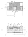
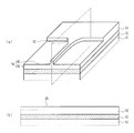
- FIG. 20 is a schematic cross-sectional view of a conventional photodetector using Ge as an absorption layer.
- the photodetector is formed using an SOI substrate.
- a Si layer 83 provided on the Si substrate 81 via a BOX layer 82 is processed to form a p-type Si mesa portion 84 and p-type Si slab portions 85 on both sides thereof.
- a striped waveguide connected to the p-type Si mesa portion 84 via a tapered portion is formed.
- a non-doped Ge layer is formed on the p-type Si mesa portion 84 by selective growth, and an n-type impurity is implanted into the surface to form an n ++ -type Ge contact layer 87.
- a type Ge light absorption layer 86 is provided.
- ap type impurity is implanted into a part of the p type Si slab portion 85 to form ap + + type Si contact portion 88.
- an oxide film 89 serving as an upper clad layer for the striped waveguide is formed, plugs 90 and 91 are formed, and an n-side electrode 92 and a p-side electrode 93 are formed.
- the light propagating through the striped waveguide propagates to the i-type Ge light absorption layer 86 through the p-type Si mesa portion and is absorbed by the evanescent coupling.
- the photodetector having the structure shown in FIG. 20 has a problem that it is impossible to simultaneously increase the wavelength bandwidth by introducing tensile strain and to improve the high-speed response characteristics and response efficiency by miniaturization.
- a substrate whose surface is a single crystal Si layer, a first conductivity type Si layer on the substrate, a non-doped Ge layer, and a second conductivity type opposite to the first conductivity type.
- a semiconductor light receiving element comprising a second conductivity type contact electrode provided on a layer and a first conductivity type contact electrode provided on the first conductivity type Si layer.
- an annealing step of activating the first conductivity type impurity by ion implantation into at least a part of the surface of the substrate whose surface is a single crystal Si layer, and at least the first conductivity type impurity A step of growing a non-doped Ge layer on the first conductivity type Si region into which ion is implanted, a step of forming a first dielectric mask covering the photodiode formation region on the surface of the non-doped Ge layer, A step of ion-implanting a second conductivity type impurity having a conductivity type opposite to the first conductivity type into the exposed portion of the non-doped Ge layer using the dielectric mask as a mask; and a step of using the first dielectric mask as a mask.
- a method for manufacturing a semiconductor light receiving element is provided.
- the disclosed semiconductor light receiving element and the method for manufacturing the same it is possible to achieve both an operation in a wide wavelength band, a high speed response, and a high response efficiency.
- FIG. 7 is a configuration explanatory diagram of a semiconductor light receiving element of Example 1 of the present invention.
- FIG. It is explanatory drawing to the middle of the manufacturing process of the semiconductor light receiving element of Example 2 of this invention. It is explanatory drawing to the middle after FIG. 11 of the manufacturing process of the semiconductor light receiving element of Example 2 of this invention. It is explanatory drawing to the middle after FIG. 12 of the manufacturing process of the semiconductor light receiving element of Example 2 of this invention. It is explanatory drawing to the middle after FIG.
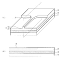
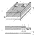
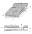
- FIG. 1 is a perspective view and a side sectional view of a semiconductor light receiving element of the present invention
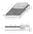
- FIG. 2 is a top view and a sectional view of the semiconductor light receiving element of the present invention.
- a PIN photodiode 15 is formed by sequentially laminating a first conductivity type Si layer 16, a non-doped Ge layer 17, and a second conductivity type Ge layer 18 on a substrate 11 whose surface is a single crystal Si layer.
- a Ge current blocking mechanism 19 is provided on at least a part of the periphery of the laminated structure including the non-doped Ge layer 17 / second conductivity type Ge layer 18, and a second conductivity type contact electrode 22 is provided on the second conductivity type Ge layer 18. .
- a first conductivity type contact electrode 23 connected to the first conductivity type Si layer 16 is provided.
- This Ge current blocking mechanism typically has a structure in which a second conductivity type Ge layer 20 and a first conductivity type Ge layer 21 are sequentially stacked in this order from the substrate 11 side.
- a thyristor structure including the conductive Si layer 16 is formed.
- the thyristor structure When a thyristor structure is formed, no reverse current flows through the thyristor structure during reverse bias below the reverse breakdown voltage. Therefore, the thyristor structure functions as a carrier block layer that prevents the diffusion of photocarriers generated in the non-doped Ge layer 17 to the periphery. As a result, the carrier path is narrowed and the element capacitance is reduced. At the same time, it becomes possible to reduce traps due to recombination and defects in the depletion layer due to photocarrier drift.
- the shape of the PIN photodiode 15 is typically a rectangular parallelepiped, and the other three side surfaces except for one side surface may be in contact with the Ge current blocking mechanism 19.
- the stripe-shaped single crystal Si core layer 24 may be connected to the first conductivity type Si layer 16 via the tapered waveguide 25 on one side surface not in contact with the Ge current blocking mechanism 19.
- the substrate 11 may be a single crystal Si substrate, but typically.
- An SOI substrate in which a single crystal Si layer 14 is provided on a crystalline Si substrate 12 with an SiO 2 film 13 interposed therebetween is used.
- the first conductivity type impurity is annealed by ion implantation of the first conductivity type impurity to at least a part of the surface of the substrate 11 whose surface is the single crystal Si layer 14.
- a non-doped Ge layer 17 is grown on the first conductivity type Si layer 16 region into which ions are implanted.
- a first dielectric mask is formed on the surface of the non-doped Ge layer 17 so as to cover the photodiode formation region, and two-conductivity type impurities are ion-implanted into the exposed portion of the non-doped Ge layer 17 using the first dielectric mask as a mask.
- the second conductivity type Ge layer 20 is formed.
- the first conductivity type impurity is implanted shallower than the second conductivity type impurity into the exposed portion of the non-doped Ge layer 17 into which the second conductivity type impurity has been implanted using the first dielectric mask as a mask, and the surface becomes the first conductivity type impurity.
- the first conductivity type Ge layer 21 is formed by compensation.
- a second dielectric mask that exposes only the photodiode formation region is formed, and a second conductivity type impurity is implanted into the surface of the non-doped Ge layer 17 exposed using the second dielectric mask as a mask.
- a two-conductivity Ge layer 18 may be formed.
- the single crystal Si layer 14 may be etched to form a tapered waveguide 25 connected to the photodiode region and a striped single crystal Si core layer 24 connected to the tapered waveguide 25.
- the growth process of the non-doped Ge layer 17 includes a first growth process that grows at a relatively low temperature in order to form a flat layer by two-dimensional growth, and a relative process capable of growing a high-quality crystal. It is desirable to use a two-stage growth process consisting of a second growth process that grows at a high temperature.
- a low pressure chemical vapor deposition method or a molecular beam epitaxial growth method is typical.
- the Ge layer is provided around the non-doped Ge layer 17 serving as the light absorption layer, the relaxation strain is suppressed and the shortening of the absorption edge of the non-doped Ge layer 17 is suppressed. Is done. At the same time, it is possible to reduce the element capacitance and the photo carrier trap due to defects. As a result, it is possible to simultaneously realize an operation in a wide wavelength band and a high speed response / response efficiency.
- FIGS. 3A to 9A are conceptual perspective views, and FIG. 3B is a cross-sectional view taken along the dashed line in FIG. 3A.
- a single crystal i-type Si layer 33 having a thickness of 0.3 ⁇ m is formed on a Si substrate 31 having a main surface of (001) through a BOX layer 32 having a thickness of 3.0 ⁇ m.
- the provided SOI substrate is prepared.
- a resist is applied on the i-type Si layer 33, the shape of the Si passive waveguide is exposed by electron beam lithography, and development by wet etching is performed.
- an Si rib type waveguide 34 including the core layer 35 and the slab portion 36 is formed by ICP (inductively coupled plasma) dry etching.
- a tapered portion 37 is provided on the side in contact with the i-type Si layer 33.
- a SiO 2 film is deposited on the entire surface by CVD, and patterning is performed to form an ion implantation mask 38 that opens only the regions where the light receiving portion and the thyristor portion are to be formed.
- B is ion-implanted using the ion implantation mask 38 as a mask.
- the implantation energy is 40 keV and the dose is 5.0 ⁇ 10 14 cm ⁇ 2 .
- the p-type Si layer 39 is formed by performing an annealing process at 1050 ° C. for activating the ion-implanted B for 1 second.
- the impurity concentration of the p-type Si layer 39 is set to 1.0 ⁇ 10 18 cm ⁇ 3 to 3.0 ⁇ 10 19 cm ⁇ 3 .
- a selective growth mask 40 made of a SiO 2 film is provided, and an i-type Ge layer 41 having a thickness of 0.8 ⁇ m is selectively grown by using a low pressure CVD method.
- GeH 4 is used as a source gas and H 2 is used as a carrier gas.
- 0.1 ⁇ m is grown at a low temperature of 400 ° C., and then 0.7 ⁇ m is grown at a high temperature of 700 ° C.
- an ion implantation mask 42 made of a SiO 2 film having an opening only in a portion where a thyristor structure is to be formed is formed.
- the entire i-type Ge layer 41 is doped by implanting P ions using the ion implantation mask 42 as a mask.
- the implantation energy is 600 keV and the dose amount is 1.0 ⁇ 10 14 cm ⁇ 2 .
- the impurity concentration of the n-type Ge layer 43 is 1.0 ⁇ 10 18 cm ⁇ 3 to 2.0 ⁇ 10 18 cm ⁇ 3 .
- the implantation energy is 100 keV and the dose is 3.0 ⁇ 10 14 cm ⁇ 2 .
- the impurity concentration in the p-type Ge layer 44 is 1.0 ⁇ 10 18 cm ⁇ 3 to 1.0 ⁇ 10 19 cm ⁇ 3 .
- an ion implantation mask 45 made of a SiO 2 film having an opening only in the photodiode formation region is newly formed.
- P is ion-implanted to form the upper 0.3 ⁇ m portion into the n-type Ge layer 46.
- the implantation energy is 40 keV
- the dose is 1.0 ⁇ 10 14 cm ⁇ 2 .
- the impurity concentration of the n-type Ge layer 46 is 4.0 ⁇ 10 18 cm ⁇ 3 to 1.0 ⁇ 10 19 cm ⁇ 3
- the impurity concentration at a position of 0.3 ⁇ m from the surface is 1.0 ⁇ 10 16. cm ⁇ 3 .
- activation annealing is performed at 1050 ° C. for 1 second to activate the implanted impurities.
- a low pressure CVD method is used to form an upper cladding layer 47 and a SiO 2 film to be a passivation film is deposited in the element portion, and then the surfaces of the SiO 2 film and the Ge layer are flattened by a CMP (chemical mechanical polishing) method. Turn into.
- a resist is applied to the flattened surface, the contact hole shape is exposed by electron beam lithography, and development by wet etching is performed.
- contact holes are formed by ICP dry etching and wet etching using HF.
- the contact hole is filled with Al.
- the resist used for forming the contact hole is removed, and at the same time, the Al deposited on the resist is lifted off to form the n-side electrode 48 and the p-side electrode 49, so that the semiconductor light-receiving element of Example 1 of the present invention
- the basic configuration of is completed.
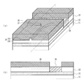
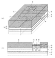
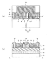
- FIG. 10 is a diagram for explaining the configuration of the semiconductor light receiving element according to the first embodiment of the present invention
- FIG. 10 (a) is a top view
- FIG. 10 (b) connects AA ′ in FIG. 10 (a). It is sectional drawing along the dashed-dotted line.
- the three side surfaces of the PIN photodiode comprising the n-type Ge layer 46 / i-type Ge layer 41 / p-type Si layer 39 are surrounded by the p-type Ge layer 44 / n-type Ge layer 43. Therefore, the effect of strain relaxation at the three end faces is suppressed from reaching the PIN type photodiode portion.
- a thyristor structure comprising an n-type Ge layer 46 / p-type Ge layer 44 / n-type Ge layer 43 / p-type Si layer 39 is formed on both side surfaces of the PIN type photodiode and functions as a current blocking layer, so that leakage occurs. The current can be reduced.
- a pseudo thyristor-like current blocking mechanism formed of n-type Ge layer 46 / p-type Ge layer 44 / n-type Ge layer 43 / i-type Si layer 33 / p-type Si layer 39 is formed. Is done.
- the signal light incident on the core layer 35 is propagated to the p-type Si layer 39 through the taper portion 37, propagated to the i-type Ge layer 41 by evanescent coupling, and absorbed, and taken out from the n-side electrode 48 as an electric signal. It is.
- the p-side electrode 49 is normally set to the ground potential.
- FIGS. 11 to 18 The basic process is the same as that of the first embodiment just by inverting the conductivity type. It is the same.
- FIG. 11A to FIG. 17A are conceptual perspective views
- FIG. 11B is a cross-sectional view taken along the dashed-dotted parallelogram in FIG.
- a single-crystal i-type Si layer 53 having a thickness of 0.3 ⁇ m is formed on a Si substrate 51 having a main surface of (001) through a BOX layer 52 having a thickness of 3.0 ⁇ m.
- the provided SOI substrate is prepared.
- a resist is applied on the i-type Si layer 53, the shape of the Si passive waveguide is exposed by electron beam lithography, and development by wet etching is performed.
- an Si rib waveguide 54 composed of the core layer 55 and the slab portion 56 is formed by ICP dry etching.
- a tapered portion 57 is provided on the side in contact with the i-type Si layer 53.
- a SiO 2 film is deposited on the entire surface by CVD, and patterning is performed to form an ion implantation mask 58 that opens only the regions where the light receiving portion and the thyristor portion are to be formed.
- P ions are implanted using the ion implantation mask 58 as a mask.
- the implantation energy is 150 keV and the dose is 5.0 ⁇ 10 14 cm ⁇ 2 .
- an n-type Si layer 59 is formed by annealing for 1 second at 1050 ° C. which activates the ion-implanted B.
- the impurity concentration of the n-type Si layer 59 is 1.0 ⁇ 10 18 cm ⁇ 3 to 3.0 ⁇ 10 19 cm ⁇ 3 .
- a selective growth mask 60 made of a SiO 2 film is provided, and an i-type Ge layer 61 having a thickness of 0.8 ⁇ m is selectively grown by using a low pressure CVD method.
- GeH 4 is used as the source gas and H 2 is used as the carrier gas.
- 0.1 ⁇ m is grown at a low temperature of 600 ° C., and then 0.7 ⁇ m is grown at a high temperature of 700 ° C.
- an ion implantation mask 62 made of an SiO 2 film having an opening only in a portion where the thyristor structure is to be formed is formed.
- the entire i-type Ge layer 61 is doped by implanting B ions using the ion implantation mask 62 as a mask.
- the implantation energy is 200 keV and the dose is 3.0 ⁇ 10 14 cm ⁇ 2 .
- the impurity concentration of the p-type Ge layer 63 is 2.0 ⁇ 10 18 cm ⁇ 3 to 6.0 ⁇ 10 18 cm ⁇ 3 .
- the ion implantation mask 62 As shown in FIG. 15, by using the same ion implantation mask 62 as a mask, P is ion-implanted shallowly, and only the upper 0.5 ⁇ m is compensated to form an n-type Ge layer 64, and the lower 0.3 ⁇ m is compensated.
- the p-type Ge layer 63 is not left.
- the implantation energy is 350 keV and the dose amount is 8.0 ⁇ 10 14 cm ⁇ 2 .
- the impurity concentration in the n-type Ge layer 64 is 1.0 ⁇ 10 18 cm ⁇ 3 to 3.0 ⁇ 10 19 cm ⁇ 3 .
- an ion implantation mask 65 made of an SiO 2 film having only the photodiode formation region opened is formed.
- B is ion-implanted to form the upper 0.3 ⁇ m portion into the p-type Ge layer 66.
- the implantation energy is 20 keV
- the dose is 2.0 ⁇ 10 14 cm ⁇ 2 .
- the impurity concentration of the p-type Ge layer 66 is 50 ⁇ 10 18 cm ⁇ 3 to 2.0 ⁇ 10 19 cm ⁇ 3 , and the impurity concentration at a position of 0.3 ⁇ m from the surface is 1.0 ⁇ 10 16 cm ⁇ . 3
- activation annealing is performed at 1050 ° C. for 1 second to activate the implanted impurities.
- an SiO 2 film that becomes the upper cladding layer 67 and a passivation film in the element portion is deposited by using a low pressure CVD method, and then the surfaces of the SiO 2 film and the Ge layer are planarized by the CMP method.
- a resist is applied to the flattened surface, the contact hole shape is exposed by electron beam lithography, and development by wet etching is performed.
- contact holes are formed by ICP dry etching and wet etching using HF.
- the contact hole is filled with Al.
- the resist used for forming the contact hole is removed, and at the same time, the Al deposited on the resist is lifted off to form the p-side electrode 68 and the n-side electrode 69, whereby the semiconductor light receiving device of the second embodiment of the present invention
- the basic configuration of is completed.
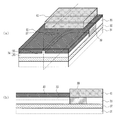
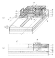
- FIG. 18A and 18B are explanatory views of the structure of the semiconductor light receiving element according to the second embodiment of the present invention.
- FIG. 18A is a top view
- FIG. 18B is a view taken along line AA ′ in FIG. It is sectional drawing along the dashed-dotted line.
- the three side surfaces of the PIN photodiode composed of the p-type Ge layer 66 / i-type Ge layer 61 / n-type Si layer 59 are surrounded by the n-type Ge layer 64 / p-type Ge layer 63. Therefore, the effect of strain relaxation at the three end faces is suppressed from reaching the PIN type photodiode portion.
- a thyristor structure including a p-type Ge layer 66 / n-type Ge layer 64 / p-type Ge layer 63 / n-type Si layer 59 is formed on both side surfaces of the PIN type photodiode and functions as a current blocking layer. The current can be reduced.
- a pseudo thyristor-like current blocking mechanism formed of p-type Ge layer 66 / n-type Ge layer 64 / p-type Ge layer 63 / i-type Si layer 53 / n-type Si layer 59 is formed. Is done.
- the signal light incident on the core layer 55 is propagated to the n-type Si layer 59 through the taper portion 57, propagated to the i-type Ge layer 61 and absorbed by evanescent coupling, and taken out from the p-side electrode 68 as an electrical signal. It is.
- the n-side electrode 69 is normally set to the ground potential.
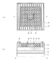
- FIG. 19A is a top view
- FIG. 19B is a cross-sectional view taken along the alternate long and short dash line connecting AA ′ in FIG. 19A.
- An SOI substrate is prepared in which a single crystal i-type Si layer having a thickness of 0.3 ⁇ m is provided on a Si substrate 71 having a main surface of (001) via a BOX layer 72 having a thickness of 3.0 ⁇ m.
- an ion implantation mask is formed on the i-type Si layer to open only the region where the light receiving portion and the thyristor portion are to be formed, and B is ion-implanted using this ion implantation mask as a mask.
- the implantation energy is 40 keV and the dose is 5.0 ⁇ 10 14 cm ⁇ 2 .
- an annealing process is performed at 1050 ° C.
- the impurity concentration of the p-type Si layer 73 is 1.0 ⁇ 10 18 cm ⁇ 3 to 3.0 ⁇ 10 19 cm ⁇ 3 .
- a selective growth mask made of an SiO 2 film is provided, and an i-type Ge layer 74 having a thickness of 0.8 ⁇ m is selectively grown on the p-type Si layer 73 by using a low pressure CVD method.
- GeH 4 is used as a source gas and H 2 is used as a carrier gas.
- 0.1 ⁇ m is grown at a low temperature of 400 ° C., and then 0.7 ⁇ m is grown at a high temperature of 700 ° C.
- an ion implantation mask made of an SiO 2 film having an opening only in a portion where the thyristor structure is to be formed is formed, and P is ion-implanted using this ion implantation mask as a mask, thereby doping the entire i-type Ge layer 74.
- the implantation energy is 600 keV and the dose amount is 1.0 ⁇ 10 14 cm ⁇ 2 .
- the impurity concentration of the n-type Ge layer 75 is 1.0 ⁇ 10 18 cm ⁇ 3 to 2.0 ⁇ 10 18 cm ⁇ 3 .
- B is ion-implanted shallowly, and only the upper 0.5 ⁇ m is compensated to form the p-type Ge layer 76, and the lower 0.3 ⁇ m is not compensated and the n-type Ge layer 75 is compensated.
- the implantation energy is 100 keV and the dose is 3.0 ⁇ 10 14 cm ⁇ 2 .
- the impurity concentration in the p-type Ge layer 76 is 1.0 ⁇ 10 18 cm ⁇ 3 to 1.0 ⁇ 10 19 cm ⁇ 3 .
- a new ion implantation mask made of a SiO 2 film having only the photodiode formation region opened is formed.
- P is ion-implanted to form the upper 0.3 ⁇ m portion into the n-type Ge layer 77.
- the implantation energy is 40 keV
- the dose is 1.0 ⁇ 10 14 cm ⁇ 2 .
- the impurity concentration of the n-type Ge layer 77 is 4.0 ⁇ 10 18 cm ⁇ 3 to 1.0 ⁇ 10 19 cm ⁇ 3
- the impurity concentration at a position of 0.3 ⁇ m from the surface is 1.0 ⁇ 10 16. cm ⁇ 3 .
- activation annealing is performed at 1050 ° C. for 1 second to activate the implanted impurities.
- the surfaces of the SiO 2 film and the Ge layer are planarized by a CMP method.
- contact holes are formed by ICP dry etching and wet etching using HF.
- the contact hole is filled with Al.
- the resist used for forming the contact hole is removed, and at the same time, Al deposited on the resist is lifted off to form the annular n-side electrode 79 and the p-side electrode 80, whereby the semiconductor according to the third embodiment of the present invention.
- the basic structure of the light receiving element is completed.
- Example 3 of the present invention since all the side surfaces of the PIN photodiode are surrounded by the p-type Ge layer 76 / n-type Ge layer 75, the effect of strain relaxation at the end is PIN type. Covering the photodiode portion is completely suppressed. Further, a thyristor structure including an n-type Ge layer 77 / p-type Ge layer 76 / n-type Ge layer 75 / p-type Si layer 73 is formed around the entire periphery of the PIN type photodiode, and functions as a current blocking layer. The current can be reduced.
- the semiconductor light receiving element of Example 3 in the drawing, light enters from above, passes through the n-type Ge layer 77, is absorbed by the i-type Ge layer 74, and is taken out from the n-side electrode 79 as an electrical signal.
- the p-side electrode 80 is set to the ground potential.
Landscapes
- Engineering & Computer Science (AREA)
- Physics & Mathematics (AREA)
- Power Engineering (AREA)
- Microelectronics & Electronic Packaging (AREA)
- General Physics & Mathematics (AREA)
- Optics & Photonics (AREA)
- Light Receiving Elements (AREA)
- Computer Networks & Wireless Communication (AREA)
- Signal Processing (AREA)
Abstract
Description
そこで、波長多重伝送を実現するためには、1.55μmより長波長の広い領域で高い応答感度を有するGeフォトディテクターが必要とされる。
12 Si基板
13 SiO2膜
14 単結晶Si層
15 PIN型フォトダイオード
16 第1導電型Si層
17 ノンドープGe層
18 第2導電型Ge層
19 Ge電流ブロック機構
20 第2導電型Ge層
21 第1導電型Ge層
22 第2導電型用コンタクト電極
23 第1導電型用コンタクト電極
24 ストライプ状単結晶Siコア層
25 テーパ導波路
26 上部クラッド層
31,51,71 Si基板
32,52,72 BOX層
33,53 i型Si層
34,54 Siリブ型導波路
35,55 コア層
36,56 スラブ部
37,57 テーパ部
38,58 イオン注入マスク
39,73 p型Si層
40,60 選択成長マスク
41,61,74 i型Ge層
42,62 イオン注入マスク
43,75 n型Ge層
44,76 p型Ge層
45,65 イオン注入マスク
46,77 n型Ge層
47,67 上部クラッド層
48,79 n側電極
49,80 p側電極
59 n型Si層
63 p型Ge層
64 n型Ge層
66 p型Ge層
68 p側電極
69 n側電極
78 パッシベーション膜
81 Si基板
82 BOX層
83 Si層
84 p型Siメサ部
85 p型Siスラブ部
86 i型Ge光吸収層
87 n++型Geコンタクト層
88 p++型Siコンタクト部
89 酸化膜
90,91 プラグ
92 n側電極
93 p側電極
Claims (10)
- 表面が単結晶Si層である基板と、
前記基板上に第1導電型Si層と、ノンドープGe層と、前記第1導電型とは反対導電型の第2導電型Ge層を順次積層したPIN型フォトダイオードと、
前記ノンドープGe層/前記第2導電型Ge層からなる積層構造の周囲の少なくとも一部に設けられたGe電流ブロック機構と、
前記第2導電型Ge層上に設けられた第2導電型用コンタクト電極と、
前記第1導電型Si層に設けられた第1導電型用コンタクト電極と
を有することを特徴とする半導体受光素子。 - 前記Ge電流ブロック機構が、基板側から順に第2導電型Ge層と第1導電型Ge層とが順次積層した構造であり、
前記第2導電型用コンタクト電極と前記第1導電型用コンタクト電極との間に第2導電型Ge層-第1導電型Ge層-第2導電型Ge層-第1導電型Si層からなるサイリスタ構造が形成されていることを特徴とする請求項1に記載の半導体受光素子。 - 前記PIN型フォトダイオードの形状が直方体状であり、一つの側面を除いた他の3つの側面が前記Ge電流ブロック機構に当接していることを特徴とする請求項2に記載の半導体受光素子。
- 前記Ge電流ブロック機構に当接していない1つの側面において、前記第1導電型Si層にストライプ状単結晶Siコア層がテーパ導波路を介して接続していることを特徴とする請求項3に記載の半導体受光素子。
- 前記PIN型フォトダイオードの全ての側面が前記Ge電流ブロック機構に囲まれており、前記PIN型フォトダイオードの頂面が光入射面であることを特徴とする請求項1または請求項2に記載の半導体受光素子。
- 前記基板が、単結晶Si基板上にSiO2膜を介して単結晶Si層が設けられたSOI基板であることを特徴とする請求項1乃至請求項5のいずれか1項に記載の半導体受光素子。
- 表面が単結晶Si層である基板の表面の少なくとも一部に第1導電型不純物をイオン注入して活性化するアニール工程と、
少なくとも前記第1導電型不純物をイオン注入した第1導電型Si領域上にノンドープGe層を成長する工程と、
前記ノンドープGe層の表面にフォトダイオード形成領域を覆う第1の誘電体マスクを形成する工程と、
前記第1の誘電体マスクをマスクとして前記ノンドープGe層の露出部に前記第1導電型とは反対の導電型である第2導電型不純物をイオン注入する工程と、
前記第1の誘電体マスクをマスクとして前記ノンドープGe層の露出部に第1導電型不純物を前記第2導電型不純物より浅く注入して表面を第1導電型不純物で補償する工程と、
前記フォトダイオード形成領域のみを露出する第2の誘電体マスクを形成する工程と、前記第2の誘電体マスクをマスクとして露出する前記ノンドープGe層の表面に第2導電型不純物を注入する工程と、
前記注入した各不純物を活性化するアニール工程と
を含むことを特徴とする半導体受光素子の製造方法。 - 前記単結晶Si層をエッチングして前記フォトダイオード領域に接続するテーパ導波路部と、前記テーパ導波路部に接続するストライプ状コア層を形成する工程を有することを特徴とする請求項7に記載の半導体受光素子の製造方法。
- 前記ノンドープGe層の成長工程が、相対的に低温で成長する第1の成長工程と、前記前記第1の成長工程より相対的に高温で成長する第2の成長工程からなる二段成長工程であることを特徴とする請求項7または請求項8に記載の半導体受光素子の製造方法。
- 前記ノンドープGe層の成長方法が、減圧化学気相成長法或いは分子ビームエピタキシャル成長法のいずれかであることを特徴とする請求項7乃至請求項9のいずれか1項に記載の半導体受光素子の製造方法。
Priority Applications (6)
| Application Number | Priority Date | Filing Date | Title |
|---|---|---|---|
| JP2015512264A JP6048578B2 (ja) | 2013-04-19 | 2013-04-19 | 半導体受光素子及びその製造方法 |
| PCT/JP2013/061625 WO2014171005A1 (ja) | 2013-04-19 | 2013-04-19 | 半導体受光素子及びその製造方法 |
| EP13882362.0A EP2988338B1 (en) | 2013-04-19 | 2013-04-19 | Semiconductor light-receiving element and method for manufacturing same |
| CN201380075744.3A CN105122469B (zh) | 2013-04-19 | 2013-04-19 | 半导体受光元件及其制造方法 |
| US14/885,056 US9401447B2 (en) | 2013-04-19 | 2015-10-16 | Semiconductor light-receiving element and method for manufacturing same |
| US15/180,198 US9577136B2 (en) | 2013-04-19 | 2016-06-13 | Semiconductor light-receiving element and method for manufacturing same |
Applications Claiming Priority (1)
| Application Number | Priority Date | Filing Date | Title |
|---|---|---|---|
| PCT/JP2013/061625 WO2014171005A1 (ja) | 2013-04-19 | 2013-04-19 | 半導体受光素子及びその製造方法 |
Related Child Applications (1)
| Application Number | Title | Priority Date | Filing Date |
|---|---|---|---|
| US14/885,056 Continuation US9401447B2 (en) | 2013-04-19 | 2015-10-16 | Semiconductor light-receiving element and method for manufacturing same |
Publications (1)
| Publication Number | Publication Date |
|---|---|
| WO2014171005A1 true WO2014171005A1 (ja) | 2014-10-23 |
Family
ID=51730974
Family Applications (1)
| Application Number | Title | Priority Date | Filing Date |
|---|---|---|---|
| PCT/JP2013/061625 Ceased WO2014171005A1 (ja) | 2013-04-19 | 2013-04-19 | 半導体受光素子及びその製造方法 |
Country Status (5)
| Country | Link |
|---|---|
| US (2) | US9401447B2 (ja) |
| EP (1) | EP2988338B1 (ja) |
| JP (1) | JP6048578B2 (ja) |
| CN (1) | CN105122469B (ja) |
| WO (1) | WO2014171005A1 (ja) |
Cited By (9)
| Publication number | Priority date | Publication date | Assignee | Title |
|---|---|---|---|---|
| JP2015162571A (ja) * | 2014-02-27 | 2015-09-07 | 富士通株式会社 | Ge系半導体装置、その製造方法及び光インターコネクトシステム |
| JP2017011020A (ja) * | 2015-06-18 | 2017-01-12 | 富士通株式会社 | Ge系光素子及びその製造方法 |
| JP2017032901A (ja) * | 2015-08-05 | 2017-02-09 | 富士通オプティカルコンポーネンツ株式会社 | 光通信装置、及び、光モジュール |
| JP2017069359A (ja) * | 2015-09-30 | 2017-04-06 | 沖電気工業株式会社 | 半導体受光素子及びその製造方法 |
| JP2019186298A (ja) * | 2018-04-04 | 2019-10-24 | 国立研究開発法人産業技術総合研究所 | 光導波路型受光素子構造 |
| JP2020106736A (ja) * | 2018-12-28 | 2020-07-09 | 日本電信電話株式会社 | 光検査回路 |
| US11409034B2 (en) * | 2020-01-29 | 2022-08-09 | Marvell Asia Pte Ltd. | Silicon photonics integration circuit |
| US11500229B2 (en) | 2019-10-16 | 2022-11-15 | Marvell Asia Pte Ltd. | Dual-slab-layer low-loss silicon optical modulator |
| US12153251B2 (en) | 2020-01-29 | 2024-11-26 | Marvell Asia Pte Ltd | Silicon photonics integration circuit |
Families Citing this family (24)
| Publication number | Priority date | Publication date | Assignee | Title |
|---|---|---|---|---|
| DE102013201644A1 (de) * | 2012-09-19 | 2014-03-20 | Ihp Gmbh - Innovations For High Performance Microelectronics / Leibniz-Institut Für Innovative Mikroelektronik | Germanium PIN-Fotodiode für die Integration in eine CMOS- oder BiCMOS-Technologie |
| US10283665B2 (en) * | 2013-07-08 | 2019-05-07 | Sifotonics Technologies Co., Ltd. | Compensated photonic device structure and fabrication method thereof |
| WO2016023105A1 (en) * | 2014-08-15 | 2016-02-18 | Aeponyx Inc. | Methods and systems for microelectromechanical packaging |
| US10680131B2 (en) * | 2015-07-27 | 2020-06-09 | Hewlett Packard Enterprise Development Lp | Doped absorption devices |
| JP2017076651A (ja) * | 2015-10-13 | 2017-04-20 | 富士通株式会社 | 半導体受光装置 |
| JP6646559B2 (ja) * | 2016-11-04 | 2020-02-14 | 日本電信電話株式会社 | 光検出器 |
| GB2572876B (en) * | 2016-11-23 | 2020-08-12 | Rockley Photonics Ltd | Electro-optically active device |
| GB2559252B (en) * | 2016-12-02 | 2020-06-03 | Rockley Photonics Ltd | Waveguide optoelectronic device |
| US10473853B2 (en) * | 2016-12-22 | 2019-11-12 | Sifotonics Technologies Co., Ltd. | Fully integrated avalanche photodiode receiver |
| US11049851B2 (en) * | 2017-06-08 | 2021-06-29 | Luxtera Llc | Method and system for selectively illuminated integrated photodetectors with configured launching and adaptive junction profile for bandwidth improvement |
| EP3714321B1 (en) * | 2017-11-23 | 2023-12-13 | Rockley Photonics Limited | Electro-optically active device |
| US12044908B2 (en) | 2018-05-16 | 2024-07-23 | Rockley Photonics Limited | III-V/SI hybrid optoelectronic device and method of manufacture |
| CN111211182A (zh) * | 2018-11-19 | 2020-05-29 | 上海新微技术研发中心有限公司 | 一种波导型光电探测器及其制造方法 |
| US10666353B1 (en) | 2018-11-20 | 2020-05-26 | Juniper Networks, Inc. | Normal incidence photodetector with self-test functionality |
| BE1027026B1 (nl) * | 2019-02-04 | 2020-09-02 | Caeleste Cvba | Gradiënt fotodiode |
| US12174424B2 (en) | 2019-11-15 | 2024-12-24 | Chamartin Laboratories Llc | Optoelectronic device and method of manufacture thereof |
| US11978812B2 (en) * | 2020-02-26 | 2024-05-07 | Mitsubishi Electric Corporation | Waveguide photodetector |
| CN112201706A (zh) * | 2020-08-31 | 2021-01-08 | 中国电子科技集团公司第三十八研究所 | 基于倏逝波耦合方式的波导集成光电探测器 |
| US11869991B2 (en) * | 2020-09-18 | 2024-01-09 | Taiwan Semiconductor Manufacturing Company Limited | Semiconductor device and method of making |
| US11588062B2 (en) * | 2020-10-08 | 2023-02-21 | Globalfoundries U.S. Inc. | Photodetectors including a coupling region with multiple tapers |
| US11949030B2 (en) * | 2020-10-27 | 2024-04-02 | Taiwan Semiconductor Manufacturing Company, Ltd. | In-situ cap for germanium photodetector |
| CN113176676B (zh) * | 2021-04-16 | 2022-11-15 | 上海曦智科技有限公司 | 光学调制器和光学集成系统 |
| US12189181B2 (en) | 2021-09-22 | 2025-01-07 | Rockley Photonics Limited | Optoelectronic device |
| US12541057B2 (en) * | 2023-07-25 | 2026-02-03 | Globalfoundries U.S. Inc. | Photonic components with chamfered sidewalls |
Family Cites Families (15)
| Publication number | Priority date | Publication date | Assignee | Title |
|---|---|---|---|---|
| DE3788841T2 (de) * | 1986-10-07 | 1994-05-05 | Sharp Kk | Halbleiterlaservorrichtung und Verfahren zur Herstellung derselben. |
| JP3828179B2 (ja) * | 1995-05-12 | 2006-10-04 | 富士通株式会社 | 半導体光検出装置およびその製造方法 |
| JP3994655B2 (ja) | 2000-11-14 | 2007-10-24 | 住友電気工業株式会社 | 半導体受光素子 |
| US20070104441A1 (en) * | 2005-11-08 | 2007-05-10 | Massachusetts Institute Of Technology | Laterally-integrated waveguide photodetector apparatus and related coupling methods |
| US7305157B2 (en) * | 2005-11-08 | 2007-12-04 | Massachusetts Institute Of Technology | Vertically-integrated waveguide photodetector apparatus and related coupling methods |
| US7418166B1 (en) * | 2006-02-24 | 2008-08-26 | The Board Of Trustees Of The Leland Stanford Junior University | Device and approach for integration of optical devices and waveguides therefor |
| US7777290B2 (en) * | 2006-06-13 | 2010-08-17 | Wisconsin Alumni Research Foundation | PIN diodes for photodetection and high-speed, high-resolution image sensing |
| WO2008080428A1 (en) * | 2006-12-29 | 2008-07-10 | Pgt Photonics S.P.A. | Waveguide photodetector in germanium on silicon |
| US7875522B2 (en) * | 2007-03-30 | 2011-01-25 | The Board Of Trustees Of The Leland Stanford Junior University | Silicon compatible integrated light communicator |
| US7745312B2 (en) * | 2008-01-15 | 2010-06-29 | Sandisk 3D, Llc | Selective germanium deposition for pillar devices |
| JP5189555B2 (ja) * | 2009-05-19 | 2013-04-24 | 日本電信電話株式会社 | 光レベル等価器 |
| JP5742345B2 (ja) * | 2011-03-20 | 2015-07-01 | 富士通株式会社 | 受光素子および光受信モジュール |
| US8455292B2 (en) * | 2011-09-09 | 2013-06-04 | International Business Machines Corporation | Deposition of germanium film |
| US8871600B2 (en) * | 2011-11-11 | 2014-10-28 | International Business Machines Corporation | Schottky barrier diodes with a guard ring formed by selective epitaxy |
| FR3015114B1 (fr) * | 2013-12-13 | 2016-01-01 | Commissariat Energie Atomique | Procede de fabrication d'un photo-detecteur |
-
2013
- 2013-04-19 EP EP13882362.0A patent/EP2988338B1/en not_active Not-in-force
- 2013-04-19 CN CN201380075744.3A patent/CN105122469B/zh not_active Expired - Fee Related
- 2013-04-19 JP JP2015512264A patent/JP6048578B2/ja not_active Expired - Fee Related
- 2013-04-19 WO PCT/JP2013/061625 patent/WO2014171005A1/ja not_active Ceased
-
2015
- 2015-10-16 US US14/885,056 patent/US9401447B2/en not_active Expired - Fee Related
-
2016
- 2016-06-13 US US15/180,198 patent/US9577136B2/en not_active Expired - Fee Related
Non-Patent Citations (7)
| Title |
|---|
| "Strain-induced enhancement of near-infrared absorption in Ge epitaxial layers grown on Si substrate", JOURNAL OF APPLIED PHYSICS, vol. 98, no. 1, 2005, pages 13501-1 - 13501-9, XP012077673 * |
| L. DING; T. Y. LIOW; A. E. J. LIM; N. DUAN; M. B. YU; G. Q. LO, OFC/NFOEC TECHNICAL DIGEST, 2012 |
| L.DING ET AL.: "Ge Waveguide Photodetectors with Responsivity Roll-off beyond 1620 nm Using Localized Stressor", OPTICAL FIBER COMMUNICATION CONFERENCE AND EXPOSITION (OFC/NFOEC), 2012 AND THE NATIONAL FIBER OPTIC ENGINEERS CONFERENCE, 2012, XP032340068 * |
| See also references of EP2988338A4 |
| TAO YIN ET AL.: "31 GHz Ge n-i-p waveguide photodetectors on Silicon-on-Insulator substrate", OPTICS EXPRESS, vol. 15, no. 21, 2007, pages 13965 - 13971, XP055233061 * |
| TAO YIN; RAMI COHEN; MIKE M. MORSE; GADI SARID; YOEL CHETRIT; DORON RUBIN; MARIO J. PANICCIA, OPTICS EXPRESS, vol. 15, 2007, pages 13966 |
| YASUHIKO ISHIKAWA; KAZUMI WADA; JIFENG LIU; DOUGLAS D. CANNON; HSIN-CHIAO LUAN; JURGEN MICHEL; LOINEL C. KIMERLING, JOURNAL OF APPLIED PHYSICS, vol. 98, 2005, pages 013501 |
Cited By (13)
| Publication number | Priority date | Publication date | Assignee | Title |
|---|---|---|---|---|
| JP2015162571A (ja) * | 2014-02-27 | 2015-09-07 | 富士通株式会社 | Ge系半導体装置、その製造方法及び光インターコネクトシステム |
| JP2017011020A (ja) * | 2015-06-18 | 2017-01-12 | 富士通株式会社 | Ge系光素子及びその製造方法 |
| US10746924B2 (en) | 2015-08-05 | 2020-08-18 | Fujitsu Optical Components Limited | Optical communication device and optical module |
| JP2017032901A (ja) * | 2015-08-05 | 2017-02-09 | 富士通オプティカルコンポーネンツ株式会社 | 光通信装置、及び、光モジュール |
| JP2017069359A (ja) * | 2015-09-30 | 2017-04-06 | 沖電気工業株式会社 | 半導体受光素子及びその製造方法 |
| JP2019186298A (ja) * | 2018-04-04 | 2019-10-24 | 国立研究開発法人産業技術総合研究所 | 光導波路型受光素子構造 |
| JP7062276B2 (ja) | 2018-04-04 | 2022-05-06 | 国立研究開発法人産業技術総合研究所 | 光導波路型受光素子構造 |
| JP2020106736A (ja) * | 2018-12-28 | 2020-07-09 | 日本電信電話株式会社 | 光検査回路 |
| JP7115305B2 (ja) | 2018-12-28 | 2022-08-09 | 日本電信電話株式会社 | 光検査回路 |
| US11815422B2 (en) | 2018-12-28 | 2023-11-14 | Nippon Telegraph And Telephone Corporation | Optical test circuit |
| US11500229B2 (en) | 2019-10-16 | 2022-11-15 | Marvell Asia Pte Ltd. | Dual-slab-layer low-loss silicon optical modulator |
| US11409034B2 (en) * | 2020-01-29 | 2022-08-09 | Marvell Asia Pte Ltd. | Silicon photonics integration circuit |
| US12153251B2 (en) | 2020-01-29 | 2024-11-26 | Marvell Asia Pte Ltd | Silicon photonics integration circuit |
Also Published As
| Publication number | Publication date |
|---|---|
| EP2988338B1 (en) | 2017-08-30 |
| JP6048578B2 (ja) | 2016-12-21 |
| US9577136B2 (en) | 2017-02-21 |
| EP2988338A1 (en) | 2016-02-24 |
| US20160293788A1 (en) | 2016-10-06 |
| CN105122469A (zh) | 2015-12-02 |
| US20160043262A1 (en) | 2016-02-11 |
| JPWO2014171005A1 (ja) | 2017-02-16 |
| CN105122469B (zh) | 2017-03-08 |
| US9401447B2 (en) | 2016-07-26 |
| EP2988338A4 (en) | 2016-05-25 |
Similar Documents
| Publication | Publication Date | Title |
|---|---|---|
| JP6048578B2 (ja) | 半導体受光素子及びその製造方法 | |
| US9653639B2 (en) | Laser using locally strained germanium on silicon for opto-electronic applications | |
| JP5232981B2 (ja) | SiGeフォトダイオード | |
| JP6793786B1 (ja) | 半導体受光素子、光電融合モジュール及びアバランシェフォトダイオードの製造方法 | |
| JP6091273B2 (ja) | 半導体装置とその製造方法 | |
| JP6378928B2 (ja) | Ge系半導体装置、その製造方法及び光インターコネクトシステム | |
| JP2017201649A (ja) | 半導体装置およびその製造方法 | |
| US10942315B2 (en) | Reducing back reflection in a photodiode | |
| JP2017076651A (ja) | 半導体受光装置 | |
| US20180090636A1 (en) | Semiconductor device and method of manufacturing the same | |
| JP2017220581A (ja) | 半導体装置及びその製造方法、光インターコネクトシステム | |
| JP6656016B2 (ja) | 半導体装置及び光インターコネクトシステム | |
| JP5824929B2 (ja) | 光半導体素子の製造方法 | |
| JP6726248B2 (ja) | 半導体受光素子、及び光電融合モジュール | |
| JP6423159B2 (ja) | Ge系半導体装置、その製造方法及び光インターコネクトシステム | |
| US11886003B2 (en) | Optical waveguide | |
| JP6696735B2 (ja) | Ge系光素子及びその製造方法 | |
| JP7125822B2 (ja) | 光半導体素子及び光伝送装置 | |
| US12527095B2 (en) | Method of fabricating Si photonics chip with integrated high speed Ge photo detector working for entire C- and L-band | |
| JP7275843B2 (ja) | 光半導体素子 | |
| Lin et al. | Germanium photodetectors with 60-nm absorption coverage extension and∼ 2× quantum efficiency enhancement across L-band | |
| CN119815942A (zh) | 一种光电探测器及其制造方法 | |
| WO2024068643A1 (en) | Photodetector and method for fabricating a photodetector |
Legal Events
| Date | Code | Title | Description |
|---|---|---|---|
| 121 | Ep: the epo has been informed by wipo that ep was designated in this application |
Ref document number: 13882362 Country of ref document: EP Kind code of ref document: A1 |
|
| ENP | Entry into the national phase |
Ref document number: 2015512264 Country of ref document: JP Kind code of ref document: A |
|
| NENP | Non-entry into the national phase |
Ref country code: DE |
|
| REEP | Request for entry into the european phase |
Ref document number: 2013882362 Country of ref document: EP |
|
| WWE | Wipo information: entry into national phase |
Ref document number: 2013882362 Country of ref document: EP |