WO2014171292A1 - コネクタ装置及び無線伝送システム - Google Patents
コネクタ装置及び無線伝送システム Download PDFInfo
- Publication number
- WO2014171292A1 WO2014171292A1 PCT/JP2014/058959 JP2014058959W WO2014171292A1 WO 2014171292 A1 WO2014171292 A1 WO 2014171292A1 JP 2014058959 W JP2014058959 W JP 2014058959W WO 2014171292 A1 WO2014171292 A1 WO 2014171292A1
- Authority
- WO
- WIPO (PCT)
- Prior art keywords
- waveguide
- connector device
- connector
- hollow
- cable
- Prior art date
- Legal status (The legal status is an assumption and is not a legal conclusion. Google has not performed a legal analysis and makes no representation as to the accuracy of the status listed.)
- Ceased
Links
Images


Classifications
-
- H—ELECTRICITY
- H01—ELECTRIC ELEMENTS
- H01P—WAVEGUIDES; RESONATORS, LINES, OR OTHER DEVICES OF THE WAVEGUIDE TYPE
- H01P5/00—Coupling devices of the waveguide type
- H01P5/08—Coupling devices of the waveguide type for linking dissimilar lines or devices
- H01P5/10—Coupling devices of the waveguide type for linking dissimilar lines or devices for coupling balanced lines or devices with unbalanced lines or devices
- H01P5/107—Hollow-waveguide/strip-line transitions
-
- H—ELECTRICITY
- H01—ELECTRIC ELEMENTS
- H01P—WAVEGUIDES; RESONATORS, LINES, OR OTHER DEVICES OF THE WAVEGUIDE TYPE
- H01P3/00—Waveguides; Transmission lines of the waveguide type
- H01P3/16—Dielectric waveguides, i.e. without a longitudinal conductor
-
- H—ELECTRICITY
- H01—ELECTRIC ELEMENTS
- H01P—WAVEGUIDES; RESONATORS, LINES, OR OTHER DEVICES OF THE WAVEGUIDE TYPE
- H01P5/00—Coupling devices of the waveguide type
- H01P5/08—Coupling devices of the waveguide type for linking dissimilar lines or devices
- H01P5/087—Transitions to a dielectric waveguide
-
- H—ELECTRICITY
- H02—GENERATION; CONVERSION OR DISTRIBUTION OF ELECTRIC POWER
- H02J—ELECTRIC POWER NETWORKS; CIRCUIT ARRANGEMENTS OR SYSTEMS FOR SUPPLYING OR DISTRIBUTING ELECTRIC POWER; SYSTEMS FOR STORING ELECTRIC ENERGY
- H02J50/00—Circuit arrangements or systems for wireless supply or distribution of electric power
- H02J50/20—Circuit arrangements or systems for wireless supply or distribution of electric power using microwaves or radio frequency waves
Definitions
- the present disclosure relates to a connector device and a wireless transmission system.
- a waveguide-microstrip line converter which is composed of an anti-podal line and is provided with a short-circuited stub of about 1/4 wavelength short-circuited on the waveguide wall, is used. (For example, refer to Patent Document 1).
- the present disclosure provides a connector device capable of arbitrarily connecting or disconnecting a circuit board and a waveguide cable, and a wireless transmission system having the connector device. Objective.
- the connector device for achieving the above object is as follows: A hollow waveguide provided on the circuit board in a state of being electromagnetically coupled to a feeder line formed on the circuit board;
- the hollow waveguide is configured to be detachably coupled to an end portion of a waveguide cable that transmits a high-frequency signal.
- the connector device for achieving the above-described object is: A hollow waveguide provided at an end of the waveguide cable in an electromagnetically coupled state with a waveguide cable transmitting a high-frequency signal;
- the hollow waveguide is configured to be detachably coupled to an end portion of a feed line formed on the circuit board.
- the connector device for achieving the above object is A first connector portion provided at an end of a feed line formed on a circuit board; A second connector provided at an end of a waveguide cable for transmitting a high-frequency signal; A coupling portion including a hollow waveguide interposed between the first connector portion and the second connector portion, and capable of detachably coupling the first connector portion and the second connector portion; It has composition which has.
- a wireless transmission system of the present disclosure for achieving the above object is A transmitter for transmitting a high-frequency signal; A receiving unit for receiving a high-frequency signal; A waveguide cable for transmitting a high-frequency signal between the transmitter and the receiver; A connector device for connecting at least one of the transmission unit and the reception unit and the waveguide cable; With Connector device A first connector portion provided at an end of a feed line formed on a circuit board; A second connector provided at an end of a waveguide cable for transmitting a high-frequency signal; A coupling portion including a hollow waveguide interposed between the first connector portion and the second connector portion, and capable of detachably coupling the first connector portion and the second connector portion; It has composition which has.
- a hollow is provided between the connector portion on the circuit board side and the connector portion on the waveguide cable side.
- a waveguide is interposed, and both the connector portions can be detachably coupled at the hollow waveguide portion.
- the circuit board side and the waveguide cable side can be arbitrarily connected, Alternatively, the connection can be released.
- the effect described in this specification is an illustration to the last, Comprising: It is not limited to this, There may be an additional effect.
- FIG. 1A is a block diagram illustrating an example of a configuration of a wireless transmission system to which the technology of the present disclosure is applied
- FIG. 1B is a block diagram illustrating an example of a specific configuration of a transmission unit and a reception unit in the wireless transmission system.
- FIG. 2A is a plan view including a partial cross section showing a state before coupling of the connector device according to the embodiment of the present disclosure
- FIG. 2B is a plan view including a partial cross section showing a state after coupling.
- FIG. 3 is a perspective view illustrating an outline of the connector device according to the first embodiment.
- 4A is a plan view of FIG. 3
- FIG. 4B is a side view of FIG. 3, and FIG.
- FIG. 4C is a cross-sectional view of a hollow waveguide and a spacer.
- 5A is a diagram illustrating an example of a configuration of a termination portion of a feed line on a circuit board
- FIG. 5B is a diagram illustrating transmission characteristics between the feed line and the waveguide cable in the case of the first embodiment. is there.
- FIG. 6 is a perspective view illustrating an outline of the connector device according to the second embodiment.
- 7A is a plan view of FIG. 6,
- FIG. 7B is a side view of FIG. 6, and
- FIG. 7C is a cross-sectional view of a hollow ridge waveguide used as a hollow waveguide.
- FIG. 8A is a diagram illustrating an example of a configuration of a termination portion of a feed line on a circuit board
- FIG. 8B is a diagram illustrating transmission characteristics between the feed line and the waveguide cable in the case of the second embodiment. is there.
- FIG. 9 is a perspective view illustrating an outline of the connector device according to the third embodiment.
- 10A is a plan view of FIG. 9,
- FIG. 10B is a side view of FIG. 9, and
- FIG. 10C is a cross-sectional view of a hollow ridge waveguide and a waveguide cable used as a hollow waveguide. Both are illustrated.
- FIG. 11A is a diagram illustrating an example of a configuration of a termination portion of a feed line on a circuit board
- FIG. 11A is a diagram illustrating an example of a configuration of a termination portion of a feed line on a circuit board
- FIG. 11B is a diagram illustrating transmission characteristics between the feed line and the waveguide cable in the case of the third embodiment. is there.
- FIG. 12A is a perspective view illustrating an outline of a connector device according to a modification
- FIG. 12B is a front view of FIG. 12A.
- FIG. 13 is a diagram illustrating transmission characteristics between the feed line and the waveguide cable in the modification.
- Wireless transmission systems that transmit electromagnetic waves, particularly high-frequency signals such as microwaves, millimeter waves, and terahertz waves, using waveguides as media are signals between various devices such as electronic devices, information processing devices, and semiconductor devices. And transmission of signals between circuit boards in one device (equipment).
- a waveguide that transmits a high-frequency signal has a function as a cable that connects devices and circuit boards, and is therefore called a waveguide cable.
- millimeter waves are radio waves having a frequency of 30 [GHz] to 300 [GHz] (wavelengths of 1 [mm] to 10 [mm]).
- Gbps for example, 5 [Gbps] or more
- signals that require high-speed signal transmission in the Gbps order include data signals such as movie images and computer images.
- signal transmission in the millimeter wave band is excellent in interference resistance, and there is an advantage that it is not necessary to disturb other electric wiring in cable connection between devices.
- the waveguide cable may be configured by a hollow waveguide or a dielectric waveguide.
- a dielectric waveguide that is more flexible than the hollow waveguide.
- the electromagnetic wave propagates through the dielectric while forming an electromagnetic field according to the wavelength (frequency) or the like.
- the circuit board and the waveguide cable, or the waveguide cable and the circuit board are coupled via a connector device.
- the connector device including the connector portion on the circuit board side is the connector device according to the first aspect
- the connector device including the connector portion on the waveguide cable side is the connector device according to the second aspect.
- a connector device including a connector portion (first connector portion) on the circuit board side and a connector portion (second connector portion) on the waveguide cable side is a connector device according to the third aspect.
- a spacer may be interposed between the hollow waveguide and the end portion of the waveguide cable.
- the spacer can be made of a hollow ridge waveguide.
- the hollow waveguide can be constituted by a hollow ridge waveguide.
- the waveguide cable can have a configuration made of a dielectric waveguide or a configuration made of a dielectric ridge waveguide.
- the hollow waveguide is provided on the circuit board in an electromagnetically coupled state with the dielectric waveguide, in other words, included in the first connector portion. Can be configured.
- the hollow waveguide is provided at the end of the waveguide cable in an electromagnetically coupled state with the end of the waveguide cable. In other words, the hollow waveguide is included in the second connector portion. Can do.
- FIG. 1A is a block diagram illustrating an example of a configuration of a wireless transmission system to which the technology of the present disclosure is applied
- FIG. 1B is a block diagram illustrating an example of a specific configuration of a transmission unit and a reception unit in the wireless transmission system. It is.
- a wireless transmission system 1 includes a transmission unit 10 that transmits a high-frequency signal, a reception unit 20 that receives a high-frequency signal, and a transmission unit 10 and a reception unit 20. And a dielectric waveguide cable (dielectric waveguide) 30 for transmitting a high-frequency signal.
- the waveguide cable may be configured with a hollow waveguide, or may be configured with a dielectric waveguide.
- the high-frequency signal is a millimeter-wave band signal (millimeter-wave communication)
- the millimeter wave communication can take a wide communication band, it is easy to increase the data rate.
- the frequency used for transmission can be separated from the frequency of other baseband signal processing, and interference between the millimeter wave and the frequency of the baseband signal hardly occurs.
- the millimeter wave band has a short wavelength, the waveguide structure determined according to the wavelength can be made small. In addition, since the distance attenuation is large and the diffraction is small, electromagnetic shielding is easy to perform.
- the stability of a carrier wave has strict regulations to prevent interference and the like.
- the transmission unit 10 performs a process of converting the signal to be transmitted into a millimeter-wave signal and outputting it to the waveguide cable 30.
- the receiving unit 20 performs a process of receiving a millimeter wave signal transmitted through the waveguide cable 30 and returning (restoring) the original signal to be transmitted.
- the transmission unit 10 is provided in the first communication device 100
- the reception unit 20 is provided in the second communication device 200.
- the waveguide cable 30 also transmits a high-frequency signal between the first communication device 100 and the second communication device 200.
- the transmission unit 10 and the reception unit 20 are combined and arranged in pairs.
- the signal transmission method between the first communication device 100 and the second communication device 200 may be a one-way (one-way) transmission method or a two-way transmission method. .
- the transmission unit 10 (first communication device 100) and the reception unit 20 (second communication device 200) are arranged within a predetermined range.
- the “predetermined range” is not limited as long as the high-frequency signal is a millimeter wave signal and the millimeter wave transmission range can be limited.
- a range in which the distance is shorter than the distance between communication devices used in broadcasting or general wireless communication corresponds to the “predetermined range”.
- the transmission unit 10 and the reception unit 20 are arranged within a predetermined range, as illustrated in FIG. 1A, separate communication devices (electronic devices), that is, the first communication device 100 and the second communication device.
- the transmission unit 10 and the reception unit 20 may be arranged on separate circuit boards in one electronic device. In the case of this form, one circuit board corresponds to the first communication device 100 and the other circuit board corresponds to the second communication device 200.
- the transmission unit 10 and the reception unit 20 are arranged on different semiconductor chips in one electronic device.
- one semiconductor chip corresponds to the first communication device 100 and the other semiconductor chip corresponds to the second communication device 200.
- positioned in the separate circuit part on the same circuit board can be considered.
- one circuit unit corresponds to the first communication device 100 and the other circuit unit corresponds to the second communication device 200.
- the first communication device 100 and the second communication device 200 for example, the following combinations can be considered.
- the combinations exemplified below are only examples, and are not limited to these combinations.
- the first communication device 100 When the second communication device 200 is a battery-powered device such as a mobile phone, a digital camera, a video camera, a game machine, or a remote controller, the first communication device 100 performs the battery charger, image processing, and the like. A combination of what is called a base station can be considered. Further, when the second communication device 200 is a device having an appearance such as a relatively thin IC card, the first communication device 100 may be a combination of card reading / writing devices. The card reading / writing device is further used in combination with an electronic device main body such as a digital recording / reproducing device, a terrestrial television receiver, a mobile phone, a game machine, or a computer. Further, in the case of application to an imaging device, for example, the first communication device 100 is on the main substrate side and the second communication device 200 is on the imaging substrate side, and signal transmission is performed within one device (device). It will be.
- a battery-powered device such as a mobile phone, a digital camera, a video camera, a
- the transmission unit 10 includes, for example, a signal generation unit 11 that processes a signal to be transmitted and generates a millimeter wave signal.
- the signal generation unit 11 is a signal conversion unit that converts a signal to be transmitted into a millimeter wave signal, and includes, for example, an ASK (Amplitude Shift Keying) modulation circuit. Specifically, the signal generation unit 11 generates a millimeter-wave ASK modulation wave by multiplying the millimeter-wave signal supplied from the oscillator 111 and the transmission target signal by the multiplier 112, and passes through the buffer 113. The output configuration is adopted.
- a connector device 40 is interposed between the transmission unit 10 and the waveguide cable 30.
- the receiving unit 20 includes, for example, a signal restoring unit 21 that processes a millimeter wave signal given through the waveguide cable 30 to restore the original transmission target signal.
- the signal restoration unit 21 is a signal conversion unit that converts a received millimeter-wave signal into an original signal to be transmitted, and includes, for example, a square (square) detection circuit.
- the signal restoration unit 21 employs a configuration in which a millimeter wave signal (ASK modulated wave) given through the buffer 211 is squared by the multiplier 212 to be converted into a transmission target signal and output through the buffer 213. ing.
- a connector device 50 is interposed between the waveguide cable 30 and the receiving unit 20.
- the waveguide cable 30 is configured with a waveguide structure that transmits millimeter waves while confining them in the waveguide, and has a characteristic of efficiently transmitting electromagnetic waves in the millimeter wave band.
- the waveguide cable 30 may be a dielectric waveguide configured to include a dielectric material having a specific dielectric constant in a certain range and a dielectric loss tangent in a certain range. .
- the “certain range” may be a range in which the relative permittivity and the dielectric loss tangent of the dielectric material are within a range in which a desired effect can be obtained.
- the characteristics of the dielectric waveguide are not determined only by the dielectric material itself, but the transmission path length and the millimeter wave frequency (wavelength) are also involved in determining the characteristics. Accordingly, the relative permittivity and dielectric loss tangent of the dielectric material are not necessarily clearly defined, but can be set as follows as an example.
- the dielectric material In order to transmit a millimeter-wave signal at high speed in the dielectric waveguide, the dielectric material has a relative dielectric constant of about 2 to 10 (preferably 3 to 6) and a dielectric loss tangent of 0.00001 to It is desirable to set it to about 0.01 (preferably 0.00001 to 0.001).
- the dielectric material satisfying such conditions include those made of acrylic resin, urethane resin, epoxy resin, silicone, polyimide, and cyanoacrylate resin.
- ⁇ Connector Device According to Embodiment>
- the present invention is not limited to the application to the connector device 40 interposed between the transmission unit 10 and the waveguide cable 30, but to the connector device 50 interposed between the waveguide cable 30 and the reception unit 20. However, it can be applied in the same manner as the connector device 40.
- the connector device is composed of a combination of a first connector part (one of male / female) and a second connector part (the other of male / female) like a so-called male / female combination.
- the connector device composed of this combination is the connector device according to the third aspect.
- the connector device according to the present embodiment is not limited to the connector device according to the third aspect.
- a connector device including only one connector portion may be used, and the connector device is the connector device according to the first aspect or the second aspect.
- the connector device according to the third aspect which is a combination of the first connector portion and the second connector portion, will be described as an example.
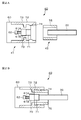
- FIG. 2A is a plan view including a partial cross section showing a state before coupling of the connector device according to the embodiment of the present disclosure (that is, the connector device according to the third aspect), and FIG. 2B is a state after coupling. It is a top view containing the partial cross section which shows.
- the connector device 40 includes a combination of a first connector portion 41 on the circuit board 60 side and a second connector portion 42 on the waveguide cable 30 side.
- the circuit board 60 is a plate-like dielectric board, and is composed of a printed board on which electronic components are fixed and wired to construct an electronic circuit.
- two feeder lines 61A and 61B are formed on the circuit board 60 so as to be parallel to each other by a linear conductor foil.
- the feed lines 61A and 61B made of linear conductor foil transmit (transmit) electromagnetic waves based on millimeter-wave band signals output from the semiconductor chip 62 in which the signal generation unit 11 of the transmission unit 10 and the like are integrated.
- a hollow waveguide 70 made of a metal such as copper or aluminum is provided at the end of the feeding lines 61A and 61B on the transmission destination side.
- the hollow waveguide 70 is provided on the circuit board 60 in a state of being electromagnetically coupled to the feeder lines 61A and 61B. Details of the electromagnetic coupling between the feeder lines 61A and 61B and the hollow waveguide 70 will be described later.
- a spacer 71 is provided on the opposite side of the hollow waveguide 70 from the feed lines 61A and 61B. The spacer 71 is interposed between the hollow waveguide 70 and the end portion of the waveguide cable 30 when the first connector portion 41 and the second connector portion 42 are coupled to each other, and performs impedance matching. Do it.
- a cylindrical first coupling portion 72 is attached so as to surround the feed lines 61A and 61B, the hollow waveguide 70, and the spacer 71.
- the first coupling portion 72 is made of plastic or the like, and has a configuration in which a stopper portion 73 and an elastically deformable protrusion 74 are formed on the inner wall thereof.
- the second connector portion 42 includes a second coupling portion 75 attached to the end portion of the waveguide cable 30.
- the second coupling portion 75 is a projection when the first coupling portion 72 of the first connector portion 41 is pushed into the first coupling portion 72 until the opening end contacts the stopper portion 73.
- the first coupling portion 72 is fixed by a reaction force accompanying the elastic deformation 74.
- first connector portion 41 and the second connector portion 42 are configured to be detachably connectable in cooperation with the first connecting portion 72 and the second connecting portion 75.
- connection structure by the 1st coupling part 72 and the 2nd coupling part 75 demonstrated here is only an example, and is not restricted to this coupling structure,
- the 1st connector part 41 and 2nd As long as it can be detachably coupled to the connector portion 42, the structure (configuration) is not limited.
- the spacer 71 is not an essential component.
- the first connector portion 41 and the second connector portion 42 are detachable.
- the waveguide cable 30 side can be arbitrarily connected to the circuit board 60 side, or the connection can be released.
- a hollow waveguide 70 made of a metal such as copper or aluminum is interposed in the coupling portion. Therefore, the connecting portion of the connector device 40 can be easily manufactured using a technique such as a mold, a sheet metal, and cutting.
- the technique of the present disclosure in which the hollow waveguide 70 is interposed and the first connector portion 41 and the second connector portion 42 are detachable is the first connector portion 41 side.
- the present invention can be similarly applied to the second connector portion 42 side.
- a hollow waveguide 70 is provided at the end of the waveguide cable 30 in an electromagnetically coupled state with the waveguide cable 30, and the first connector portion 41 is connected via the hollow waveguide 70.
- the second connector portion 42 may be configured to be detachable. At this time, it is possible to adopt a configuration in which a spacer 71 for impedance matching is interposed between the hollow waveguide 70 and the ends of the feed lines 61A and 61B.
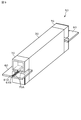
- FIG. 3 is a perspective view illustrating an outline of the connector device according to the first embodiment.
- 4A is a plan view of FIG. 3
- FIG. 4B is a side view of FIG. 3
- FIG. 4C is a cross-sectional view of the hollow waveguide and the spacer.
- FIG. 1B both the connector device 40 interposed between the transmission unit 10 and the waveguide cable 30 and the connector device 50 interposed between the reception unit 20 and the waveguide cable 30 are illustrated. Show.
- a dielectric waveguide having a dielectric constant of 2.1 is used as the waveguide cable 30.
- the size of the dielectric waveguide for example, the height is set to about 3 [mm] and the width is set to about 1.5 [mm].
- the spacer 71 is a hollow ridge waveguide made of a metal such as copper or aluminum.
- the size of the hollow ridge waveguide (ridge 71) for example, the height is set to about 3.6 [mm] and the width is set to about 1.5 [mm].
- the size of the ridge portion 71A of the hollow ridge waveguide (ridge 71) is set to a height of about 1 [mm] and a width of about 0.2 [mm].
- the size of the hollow waveguide 70 is set to, for example, a height of 4.3 [mm], a width of 1.5 [mm], and a length of about 1.4 [mm]. Then, the waveguide is formed so that the length between the end surface of the hollow waveguide 70 on the transmission unit 10 side and the end surface of the hollow waveguide 70 on the reception unit 20 side is, for example, about 10 [mm].
- the lengths of the cable 30 and the hollow ridge waveguide (ridge 71) are set.
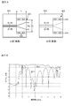
- FIG. 5A shows an example of the configuration of the terminal portions of the feeder lines 61A and 61B on the circuit board 60.
- FIG. 5A shows the configuration of the A surface (front surface) of the circuit board 60
- the right diagram of FIG. 5A shows the configuration of the B surface (back surface) of the circuit board 60.
- the circuit board 60 for example, a double-sided board having a thickness of 0.2 [mm] and a relative dielectric constant of 4.3 is used.
- the distance between the two feeder lines 61A and 61B and the line width of the feeder lines 61A and 61B are set according to the characteristic impedance of the waveguide cable 30.
- the shape of the opening pattern portion 43 is a tapered shape.
- the shape is not limited to this, and may be a shape that gradually spreads stepwise toward the edge of the circuit board 60, for example.
- the length L from the end of the feed lines 61A and 61B to the opening end is determined according to the wavelength ⁇ of the radio wave.
- the wavelength ⁇ of the radio wave here is not the wavelength of the radio wave in free space (in the air) but the wavelength of the radio wave in the circuit board 60. Since the relative permittivity of the circuit board 60 is higher than the relative permittivity of the free space, the wavelength ⁇ of the radio wave in the circuit board 60 is shorter than the wavelength of the radio wave in the free space. Accordingly, the length L of the tapered portion is determined according to the wavelength ⁇ of the radio wave in the circuit board 60.
- the length L of the tapered portion is set to about 1.4 [mm].
- the conductive pattern portion 44 is also formed on the back surface (B surface).
- the opening pattern portion 43 is electrically connected to the conductive pattern portion 44 via the via 45.
- the electromagnetic waves (electromagnetic field distribution) transmitted by the feed lines 61A and 61B are within the substrate surface of the circuit board 60 ( It is enlarged in the horizontal plane) and radiated into the hollow waveguide 70.
- signal transmission is performed by electromagnetic induction (electromagnetic coupling) between the end portions of the feeder lines 61 ⁇ / b> A and 61 ⁇ / b> B, that is, between the opening pattern portion 43 and the hollow waveguide 70.
- the electromagnetic coupling between the feeder lines 61A and 61B and the hollow waveguide 70 is a horizontal electric field type coupling.
- the width W 1 and the opening width W 2 of the opening end of the opening pattern portion 43 are set to It is decided according to the size.
- the two long sides of the hollow waveguide 70 intersect the electric field. Therefore, for the hollow waveguide 70 having a width of 1.5 [mm], as an example, the width W 1 of the opening end of the opening pattern portion 43 is 1.5 [mm] and the opening width W 2 is 0.7. It is set to about [mm].
- the connector device according to the first embodiment is applied to a wireless transmission system that uses a dielectric waveguide that is superior to a hollow waveguide as the waveguide cable 30.
- application to a wireless transmission system using a hollow waveguide as the waveguide cable 30 is not excluded.
- FIG. 5B shows transmission characteristics between the feeder lines 61A and 61B and the waveguide cable 30 in the case of the first embodiment.
- S11 is the reflection coefficient of the S parameter
- S21 is the transmission coefficient of the S parameter.
- the waveguide cable 30 made of a dielectric waveguide has a low cutoff frequency because the dielectric is clogged in the waveguide.
- the hollow waveguides have the same size, the cutoff frequency increases.
- the hollow ridge waveguide is interposed between the hollow waveguide 70 and the waveguide cable 30, so that the cut-off frequency is lower than that of the hollow waveguide. Impedance matching between the feeder lines 61A and 61B and the waveguide cable 30 is easier than in the case of 70 alone.
- FIG. 6 is a perspective view illustrating an outline of the connector device according to the second embodiment.
- 7A is a plan view of FIG. 6,
- FIG. 7B is a side view of FIG. 6, and
- FIG. 7C is a cross-sectional view of a hollow ridge waveguide used as a hollow waveguide.
- a hollow ridge waveguide is used as the hollow waveguide 70 and the spacer 71 is omitted.
- the other configuration is basically the same as that of the first embodiment.
- the size of the hollow ridge waveguide (hollow waveguide 70) for example, the height is set to about 3 [mm] and the width is set to about 1.5 [mm].
- the size of the ridge portion 70A of the hollow ridge waveguide (70) is set to a height of about 0.2 [mm] and a width of about 0.55 [mm].
- FIG. 8A shows an example of the configuration of the terminal portions of the feeder lines 61A and 61B on the circuit board 60.
- FIG. 8A shows the configuration of the A surface of the circuit board 60
- the right diagram of FIG. 8A shows the configuration of the B surface of the circuit board 60.
- the configuration of the opening pattern portion 43 at the end of the feeder lines 61A and 61B is basically the same as that in the first embodiment. However, in Example 2, the length L of the tapered portion in the opening pattern portion 43 is set to about 1.3 [mm].
- FIG. 8B shows signal transmission characteristics between the feed line and the waveguide cable in the second embodiment.
- S11 is the reflection coefficient of the S parameter
- S21 is the transmission coefficient of the S parameter.
- FIG. 9 is a perspective view illustrating an outline of the connector device according to the third embodiment.
- 10A is a plan view of FIG. 9,
- FIG. 10B is a side view of FIG. 9, and
- FIG. 10C is a cross-sectional view of a hollow ridge waveguide and a waveguide cable used as a hollow waveguide. is there.
- a hollow ridge waveguide is used as the hollow waveguide 70, the spacer 71 is omitted, and a dielectric ridge waveguide is used as the waveguide cable 30.
- the dielectric constant of the dielectric of the dielectric ridge waveguide used as the waveguide cable 30 is 2.1, for example.
- the size of the dielectric ridge waveguide (waveguide cable 30) is set, for example, to a height of about 3 [mm] and a width of about 1.5 [mm].
- the size of the ridge portion 30A of the dielectric ridge waveguide (30) is set to a height of about 0.2 [mm] and a width of about 0.35 [mm].
- FIG. 11A shows an example of the configuration of the terminal portions of the feed lines 61A and 61B on the circuit board 60.
- FIG. 11A shows the configuration of the A surface of the circuit board 60
- the right diagram of FIG. 8A shows the configuration of the B surface of the circuit board 60.
- the configuration of the opening pattern portion 43 at the end of the feeder lines 61A and 61B is basically the same as that in the second embodiment.
- the waveguide cable 30 has a dielectric ridge waveguide structure. Compared with the wave tube structure, there is an advantage that signal transmission characteristics can be improved.
- FIG. 11B shows signal transmission characteristics between the feeder line and the waveguide cable in the third embodiment.
- S11 is the reflection coefficient of the S parameter
- S21 is the transmission coefficient of the S parameter.
- FIG. 12A is a perspective view illustrating an outline of a connector device according to a modification
- FIG. 12B is a front view of FIG. 12A.
- the waveguide cable 30 is disposed sideways, that is, with the long side on the horizontal plane and the short side on the vertical plane.
- the waveguide cable 30 is made of a dielectric waveguide, for example.
- the size of the waveguide cable 30 is set to 1 ⁇ 2 [mm].
- the relative dielectric constant of the dielectric is 4.0.
- the horizontal waveguide cable 30 is electromagnetically coupled by the vertical electric field type from the feed lines 61A and 61B on the circuit board 60 via the ridge waveguide 80.
- the electric field intersects the two surfaces on the long side of the waveguide cable 30.
- the ridge waveguide 80 includes two members, that is, an upper member 80A and a lower member 80B, and the upper member 80A and the lower member 80B are coupled with the circuit board 60 interposed therebetween as shown in FIG. 12B. become.
- a ridge 81 is provided on the upper member 80A.
- the width of the inner wall is set to 2 [mm] and the height is set to 1 [mm].
- the length of the ridge waveguide 80 is determined according to the wavelength ⁇ of the radio wave.
- the wavelength ⁇ of the radio wave here is not the wavelength of the radio wave in free space (in the air) but the wavelength of the radio wave in the circuit board 60. Therefore, the length of the ridge waveguide 80 is determined according to the wavelength ⁇ of the radio wave in the circuit board 60 and is set to a value of about ⁇ / 4, for example, 0.75 [mm].
- the frequency is adjusted by the length of the ridge waveguide 80.
- FIG. 13 shows signal transmission characteristics between the feeder line and the waveguide cable in the case of the modification (vertical electric field type coupling).
- S11 and S22 are reflection coefficients of S parameters
- S21 is a transmission coefficient of S parameters.
- this indication can also take the following structures.
- Connector device ... first aspect A hollow waveguide provided on the circuit board in a state of being electromagnetically coupled to a feeder line formed on the circuit board;
- the hollow waveguide is a connector device that can be detachably coupled to an end portion of a waveguide cable that transmits a high-frequency signal.
- the connector device according to [A01] in which a spacer is interposed between the hollow waveguide and the end portion of the waveguide cable.
- the spacer includes a hollow waveguide.
- the connector device according to [A01] wherein the hollow waveguide is a hollow ridge waveguide.
- the hollow waveguide is a connector device that can be detachably coupled to an end of a feed line formed on a circuit board.
- the connector device according to [B02], wherein the spacer is formed of a hollow waveguide.
- the connector device according to [B01], wherein the hollow waveguide is a hollow ridge waveguide.
- a first connector portion provided at an end of a feed line formed on a circuit board;
- a second connector provided at an end of a waveguide cable for transmitting a high-frequency signal;
- a coupling portion including a hollow waveguide interposed between the first connector portion and the second connector portion, and capable of detachably coupling the first connector portion and the second connector portion;
- a connector device [C02] The connector device according to [C01], wherein the hollow waveguide is provided on the circuit board in an electromagnetically coupled state with an end portion of the feeder line.
- [C03] The connector device according to [C02], in which a spacer is interposed between the hollow waveguide and the end portion of the waveguide cable.
- [C07] The connector device according to [C06], wherein the spacer is a hollow waveguide.
- Wireless transmission system A transmitter for transmitting a high-frequency signal; A receiving unit for receiving a high-frequency signal; A waveguide cable for transmitting a high-frequency signal between the transmitter and the receiver; A connector device for connecting at least one of the transmission unit and the reception unit and the waveguide cable; With Connector device A first connector portion provided at an end of a feed line formed on a circuit board; A second connector provided at an end of a waveguide cable for transmitting a high-frequency signal; A coupling portion including a hollow waveguide interposed between the first connector portion and the second connector portion, and capable of detachably coupling the first connector portion and the second connector portion; A wireless transmission system.
Landscapes
- Engineering & Computer Science (AREA)
- Computer Networks & Wireless Communication (AREA)
- Power Engineering (AREA)
- Waveguide Connection Structure (AREA)
- Waveguides (AREA)
Abstract
Description
回路基板上に形成された給電線路と電磁結合した状態で回路基板上に設けられた中空導波管を有し、
中空導波管は、高周波の信号を伝送する導波管ケーブルの端部に対して着脱自在に結合可能な構成となっている。
高周波の信号を伝送する導波管ケーブルと電磁結合した状態で当該導波管ケーブルの端部に設けられた中空導波管を有し、
中空導波管は、回路基板上に形成された給電線路の端部に対して着脱自在に結合可能な構成となっている。
回路基板上に形成された給電線路の端部に設けられた第1のコネクタ部と、
高周波の信号を伝送する導波管ケーブルの端部に設けられた第2のコネクタ部と、
第1のコネクタ部と第2のコネクタ部との間に介在する中空導波管を含み、第1のコネクタ部と第2のコネクタ部とを着脱自在に結合可能な結合部と、
を有する構成となっている。
高周波の信号を送信する送信部と、
高周波の信号を受信する受信部と、
送信部と受信部との間で高周波の信号を伝送する導波管ケーブルと、
送信部及び受信部の少なくとも一方と導波管ケーブルとを接続するコネクタ装置と、
を備え、
コネクタ装置は、
回路基板上に形成された給電線路の端部に設けられた第1のコネクタ部と、
高周波の信号を伝送する導波管ケーブルの端部に設けられた第2のコネクタ部と、
第1のコネクタ部と第2のコネクタ部との間に介在する中空導波管を含み、第1のコネクタ部と第2のコネクタ部とを着脱自在に結合可能な結合部と、
を有する構成となっている。
尚、本明細書に記載された効果はあくまで例示であって、これに限定されるものではなく、また付加的な効果があってもよい。
1.本開示のコネクタ装置及び無線伝送システム、全般に関する説明
2.本開示の技術が適用される無線伝送システム
3.実施形態に係るコネクタ装置
3-1.実施例1(水平電界型結合:誘電体導波管を用いる例)
3-2.実施例2(水平電界型結合:中空リッジ導波管を用いる例)
3-3.実施例3(水平電界型結合:誘電体リッジ導波管を用いる例)
4.変形例(垂直電界型結合の例)
電磁波、特に、マイクロ波、ミリ波、テラヘルツ波などの高周波の信号を、導波管を媒体として伝送する無線伝送システムは、電子機器、情報処理装置、半導体装置などの各種の装置相互間の信号の伝送や、1つの装置(機器)における回路基板相互間の信号の伝送などに用いて好適なものである。この無線伝送システムにおいて、高周波の信号を伝送する導波管は、装置相互間や回路基板相互間を接続するケーブルとしての機能を持つことから、導波管ケーブルと呼称される。
本開示の技術が適用される無線伝送システムの構成の一例について、図1A及び図1Bを用いて説明する。図1Aは、本開示の技術が適用される無線伝送システムの構成の一例を示すブロック図であり、図1Bは、無線伝送システムにおける送信部及び受信部の具体的な構成の一例を示すブロック図である。
因みに、高周波の信号がミリ波帯の信号(ミリ波通信)であることで、次のような利点がある。
b)伝送に使う周波数が他のベースバンド信号処理の周波数から離すことができ、ミリ波とベースバンド信号の周波数の干渉が起こり難い。
c)ミリ波帯は波長が短いため、波長に応じて決まる導波構造を小さくできる。加えて、距離減衰が大きく回折も少ないため電磁シールドが行ない易い。
d)通常の無線通信では、搬送波の安定度については、干渉などを防ぐために厳しい規制がある。そのような安定度の高い搬送波を実現するためには、高い安定度の外部周波数基準部品と逓倍回路やPLL(位相同期ループ回路)などが用いられ、回路規模が大きくなる。これに対して、ミリ波通信では、容易に外部に漏れないようにできるとともに、安定度の低い搬送波を伝送に使用することができ、回路規模の増大を抑えることができる。
本実施形態では、送信部10と導波管ケーブル30との間に介在するコネクタ装置40に適用する場合を例に挙げて説明する。但し、送信部10と導波管ケーブル30との間に介在するコネクタ装置40への適用に限られるものではなく、導波管ケーブル30と受信部20との間に介在するコネクタ装置50に対しても、コネクタ装置40の場合と同様に適用可能である。
図3は、実施例1に係るコネクタ装置の概略を示す斜視図である。また、図4Aは、図3の平面図であり、図4Bは、図3の側面図であり、図4Cは、中空導波管及びスペーサの断面図である。ここでは、図1Bにおいて、送信部10と導波管ケーブル30との間に介在するコネクタ装置40、及び、受信部20と導波管ケーブル30との間に介在するコネクタ装置50の双方について図示している。
図6は、実施例2に係るコネクタ装置の概略を示す斜視図である。また、図7Aは、図6の平面図であり、図7Bは、図6の側面図であり、図7Cは、中空導波管として用いる中空リッジ導波管の断面図である。
図9は、実施例3に係るコネクタ装置の概略を示す斜視図である。また、図10Aは、図9の平面図であり、図10Bは、図9の側面図であり、図10Cは、中空導波管として用いる中空リッジ導波管及び導波管ケーブルの断面図である。
実施例1~実施例3にあってはいずれも、給電線路61A,61Bと中空導波管70との間の電磁結合が水平電界型の結合の場合の例であるが、本開示の技術は、水平電界型の結合への適用に限らず、垂直電界型の結合への適用も可能である。垂直電界型の結合の場合の一例について変形例として、図12A及び図12Bを用いてその概略について説明する。図12Aは、変形例に係るコネクタ装置の概略を示す斜視図であり、図12Bは、図12Aの正面図である。
[A01]《コネクタ装置・・・第1の態様》
回路基板上に形成された給電線路と電磁結合した状態で回路基板上に設けられた中空導波管を有し、
中空導波管は、高周波の信号を伝送する導波管ケーブルの端部に対して着脱自在に結合可能であるコネクタ装置。
[A02]中空導波管と導波管ケーブルの端部との間にスペーサが介在している上記[A01]に記載のコネクタ装置。
[A03]スペーサは、中空導波管から成る上記[A02]に記載のコネクタ装置。
[A04]中空導波管は、中空リッジ導波管である上記[A01]に記載のコネクタ装置。
[A05]導波管ケーブルは、誘電体導波管から成る上記[A01]から上記[A045]のいずれかに記載のコネクタ装置。
[A06]導波管ケーブルは、誘電体リッジ導波管から成る上記[A01]から上記[A04]のいずれかに記載のコネクタ装置。
[A07]高周波の信号は、ミリ波帯の信号である上記[A01]から上記[A06]のいずれかに記載のコネクタ装置。
[A08]導波管ケーブルは、ミリ波帯の信号を導波管内に閉じ込めつつ伝送する上記[A07]に記載のコネクタ装置。
[B01]《コネクタ装置・・・第2の態様》
高周波の信号を伝送する導波管ケーブルと電磁結合した状態で当該導波管ケーブルの端部に設けられた中空導波管を有し、
中空導波管は、回路基板上に形成された給電線路の端部に対して着脱自在に結合可能であるコネクタ装置。
[B02]中空導波管と導波管ケーブルの端部との間にスペーサが介在している上記[B01]に記載のコネクタ装置。
[B03]スペーサは、中空導波管から成る上記[B02]に記載のコネクタ装置。
[B04]中空導波管は、中空リッジ導波管である上記[B01]に記載のコネクタ装置。
[B05]導波管ケーブルは、誘電体導波管から成る上記[B01]から上記[B045]のいずれかに記載のコネクタ装置。
[B06]導波管ケーブルは、誘電体リッジ導波管から成る上記[B01]から上記[B04]のいずれかに記載のコネクタ装置。
[B07]高周波の信号は、ミリ波帯の信号である上記[B01]から上記[B06]のいずれかに記載のコネクタ装置。
[B08]導波管ケーブルは、ミリ波帯の信号を導波管内に閉じ込めつつ伝送する上記[B07]に記載のコネクタ装置。
[C01]《コネクタ装置・・・第3の態様》
回路基板上に形成された給電線路の端部に設けられた第1のコネクタ部と、
高周波の信号を伝送する導波管ケーブルの端部に設けられた第2のコネクタ部と、
第1のコネクタ部と第2のコネクタ部との間に介在する中空導波管を含み、第1のコネクタ部と第2のコネクタ部とを着脱自在に結合可能な結合部と、
を有するコネクタ装置。
[C02]中空導波管は、給電線路の端部と電磁結合した状態で回路基板上に設けられている上記[C01]に記載のコネクタ装置。
[C03]中空導波管と導波管ケーブルの端部との間にスペーサが介在している上記[C02]に記載のコネクタ装置。
[C04]スペーサは、中空導波管から成る上記[C03]に記載のコネクタ装置。
[C05]中空導波管は、導波管ケーブルの端部と電磁結合した状態で当該導波管ケーブルの端部に設けられている上記[C01]に記載のコネクタ装置。
[C06]中空導波管と導波管ケーブルの端部との間にスペーサが介在している上記[C05]に記載のコネクタ装置。
[C07]スペーサは、中空導波管から成る上記[C06]に記載のコネクタ装置。
[C08]中空導波管は、中空リッジ導波管である上記[C01]に記載のコネクタ装置。
[C09]導波管ケーブルは、誘電体導波管から成る上記[C01]から上記[C085]のいずれかに記載のコネクタ装置。
[C10]導波管ケーブルは、誘電体リッジ導波管から成る上記[C01]から上記[C08]のいずれかに記載のコネクタ装置。
[C11]高周波の信号は、ミリ波帯の信号である上記[C01]から上記[C10]のいずれかに記載のコネクタ装置。
[C12]導波管ケーブルは、ミリ波帯の信号を導波管内に閉じ込めつつ伝送する上記[C11]に記載のコネクタ装置。
[D01]《無線伝送システム》
高周波の信号を送信する送信部と、
高周波の信号を受信する受信部と、
送信部と受信部との間で高周波の信号を伝送する導波管ケーブルと、
送信部及び受信部の少なくとも一方と導波管ケーブルとを接続するコネクタ装置と、
を備え、
コネクタ装置は、
回路基板上に形成された給電線路の端部に設けられた第1のコネクタ部と、
高周波の信号を伝送する導波管ケーブルの端部に設けられた第2のコネクタ部と、
第1のコネクタ部と第2のコネクタ部との間に介在する中空導波管を含み、第1のコネクタ部と第2のコネクタ部とを着脱自在に結合可能な結合部と、
を有する無線伝送システム。
[D02]中空導波管は、給電線路の端部と電磁結合した状態で回路基板上に設けられている上記[D01]に記載のコネクタ装置。
[D03]中空導波管と導波管ケーブルの端部との間にスペーサが介在している上記[D02]に記載のコネクタ装置。
[D04]スペーサは、中空導波管から成る上記[D03]に記載のコネクタ装置。
[D05]中空導波管は、導波管ケーブルの端部と電磁結合した状態で当該導波管ケーブルの端部に設けられている上記[D01]に記載のコネクタ装置。
[D06]中空導波管と導波管ケーブルの端部との間にスペーサが介在している上記[D05]に記載のコネクタ装置。
[D07]スペーサは、中空導波管から成る上記[D06]に記載のコネクタ装置。
[D08]中空導波管は、中空リッジ導波管である上記[D01]に記載のコネクタ装置。
[D09]導波管ケーブルは、誘電体導波管から成る上記[D01]から上記[D085]のいずれかに記載のコネクタ装置。
[D10]導波管ケーブルは、誘電体リッジ導波管から成る上記[D01]から上記[D08]のいずれかに記載のコネクタ装置。
[D11]高周波の信号は、ミリ波帯の信号である上記[D01]から上記[D10]のいずれかに記載のコネクタ装置。
[D12]導波管ケーブルは、ミリ波帯の信号を導波管内に閉じ込めつつ伝送する上記[D11]に記載のコネクタ装置。
Claims (20)
- 回路基板上に形成された給電線路と電磁結合した状態で回路基板上に設けられた中空導波管を有し、
中空導波管は、高周波の信号を伝送する導波管ケーブルの端部に対して着脱自在に結合可能であるコネクタ装置。 - 中空導波管と導波管ケーブルの端部との間にスペーサが介在している請求項1に記載のコネクタ装置。
- スペーサは、中空導波管から成る請求項2に記載のコネクタ装置。
- 中空導波管は、中空リッジ導波管である請求項1に記載のコネクタ装置。
- 導波管ケーブルは、誘電体導波管から成る請求項1に記載のコネクタ装置。
- 導波管ケーブルは、誘電体リッジ導波管から成る請求項1に記載のコネクタ装置。
- 高周波の信号は、ミリ波帯の信号である請求項1に記載のコネクタ装置。
- 高周波の信号を伝送する導波管ケーブルと電磁結合した状態で当該導波管ケーブルの端部に設けられた中空導波管を有し、
中空導波管は、回路基板上に形成された給電線路の端部に対して着脱自在に結合可能であるコネクタ装置。 - 中空導波管と給電線路の端部との間にスペーサが介在している請求項8に記載のコネクタ装置。
- スペーサは、中空導波管から成る請求項9に記載のコネクタ装置。
- 中空導波管は、中空リッジ導波管である請求項8に記載のコネクタ装置。
- 導波管ケーブルは、誘電体導波管から成る請求項8に記載のコネクタ装置。
- 導波管ケーブルは、誘電体リッジ導波管から成る請求項8に記載のコネクタ装置。
- 高周波の信号は、ミリ波帯の信号である請求項8に記載のコネクタ装置。
- 回路基板上に形成された給電線路の端部に設けられた第1のコネクタ部と、
高周波の信号を伝送する導波管ケーブルの端部に設けられた第2のコネクタ部と、
第1のコネクタ部と第2のコネクタ部との間に介在する中空導波管を含み、第1のコネクタ部と第2のコネクタ部とを着脱自在に結合可能な結合部と、
を有するコネクタ装置。 - 中空導波管は、給電線路の端部と電磁結合した状態で回路基板上に設けられている請求項15に記載のコネクタ装置。
- 中空導波管は、導波管ケーブルの端部と電磁結合した状態で当該導波管ケーブルの端部に設けられている請求項15に記載のコネクタ装置。
- 高周波の信号は、ミリ波帯の信号である請求項15に記載のコネクタ装置。
- 高周波の信号を送信する送信部と、
高周波の信号を受信する受信部と、
送信部と受信部との間で高周波の信号を伝送する導波管ケーブルと、
送信部及び受信部の少なくとも一方と導波管ケーブルとを接続するコネクタ装置と、
を備え、
コネクタ装置は、
回路基板上に形成された給電線路の端部に設けられた第1のコネクタ部と、
高周波の信号を伝送する導波管ケーブルの端部に設けられた第2のコネクタ部と、
第1のコネクタ部と第2のコネクタ部との間に介在する中空導波管を含み、第1のコネクタ部と第2のコネクタ部とを着脱自在に結合可能な結合部と、
を有する無線伝送システム。 - 高周波の信号は、ミリ波帯の信号である請求項19に記載の無線伝送システム。
Priority Applications (4)
| Application Number | Priority Date | Filing Date | Title |
|---|---|---|---|
| CN201480020557.XA CN105144467B (zh) | 2013-04-18 | 2014-03-27 | 连接器装置和无线传输系统 |
| US14/783,565 US9728833B2 (en) | 2013-04-18 | 2014-03-27 | Connector apparatus and radio transmission system |
| EP14785444.2A EP2988365B1 (en) | 2013-04-18 | 2014-03-27 | Connector device and wireless transmission system |
| JP2015512388A JP6381522B2 (ja) | 2013-04-18 | 2014-03-27 | コネクタ装置及び無線伝送システム |
Applications Claiming Priority (2)
| Application Number | Priority Date | Filing Date | Title |
|---|---|---|---|
| JP2013-087059 | 2013-04-18 | ||
| JP2013087059 | 2013-04-18 |
Publications (1)
| Publication Number | Publication Date |
|---|---|
| WO2014171292A1 true WO2014171292A1 (ja) | 2014-10-23 |
Family
ID=51731244
Family Applications (1)
| Application Number | Title | Priority Date | Filing Date |
|---|---|---|---|
| PCT/JP2014/058959 Ceased WO2014171292A1 (ja) | 2013-04-18 | 2014-03-27 | コネクタ装置及び無線伝送システム |
Country Status (5)
| Country | Link |
|---|---|
| US (1) | US9728833B2 (ja) |
| EP (1) | EP2988365B1 (ja) |
| JP (1) | JP6381522B2 (ja) |
| CN (1) | CN105144467B (ja) |
| WO (1) | WO2014171292A1 (ja) |
Cited By (1)
| Publication number | Priority date | Publication date | Assignee | Title |
|---|---|---|---|---|
| JP2019068415A (ja) * | 2017-09-28 | 2019-04-25 | ティーイー コネクティビティ ジャーマニー ゲゼルシャフト ミット ベシュレンクテル ハフツンクTE Connectivity Germany GmbH | 低損失プラグ接続装置、および、少なくとも1つのそのようなプラグ接続装置を有するシステム |
Families Citing this family (19)
| Publication number | Priority date | Publication date | Assignee | Title |
|---|---|---|---|---|
| US9728834B2 (en) * | 2013-04-22 | 2017-08-08 | Sony Semiconductor Solutions Corporation | Connector apparatus and wireless transmission system |
| FR3022696A1 (fr) * | 2014-06-24 | 2015-12-25 | St Microelectronics Sa | Connecteur pour guide d'ondes plastique |
| US10142256B2 (en) * | 2015-07-09 | 2018-11-27 | Maxlinear, Inc. | Time and frequency allocation for concurrent communications on a shared coaxial cable |
| FR3051075B1 (fr) * | 2016-05-03 | 2019-06-28 | Universite de Bordeaux | Ensemble pour la propagation d'ondes dans la gamme de frequences comprises entre 1 ghz et 10 thz |
| KR102719400B1 (ko) | 2017-01-05 | 2024-10-21 | 인텔 코포레이션 | Mm파 커넥터 인터페이스에 내장되는 멀티플렉서 및 콤바이너 구조체들 |
| DE112017006740T5 (de) * | 2017-01-05 | 2019-09-26 | Intel Corporation | Steckbares mm-wellenmodul für rack-scale-architektur- (rsa) server und high performance computer (hpcs) |
| EP3355419B1 (de) * | 2017-01-25 | 2019-03-27 | Rosenberger Hochfrequenztechnik GmbH & Co. KG | Steckverbinder zur verbindung eines wellenleiters mit wenigstens einem elektrischen leiter |
| EP3382792B1 (en) * | 2017-03-30 | 2021-06-09 | TE Connectivity Germany GmbH | Microwave connector assembly |
| DE102017126069A1 (de) | 2017-11-08 | 2019-06-27 | Rosenberger Hochfrequenztechnik Gmbh & Co. Kg | Element zur Konversion zwischen mindestens einer linear polarisierten und mindestens einer elliptisch polarisierten elektromagnetischen Welle in einem Hohlleiter |
| DE102017126112A1 (de) | 2017-11-08 | 2019-05-23 | Rosenberger Hochfrequenztechnik Gmbh & Co. Kg | Ein- und Auskopplungsvorrichtung zwischen einem Schaltungsträger und einem Wellenleiter |
| US10826146B2 (en) | 2018-02-09 | 2020-11-03 | Marvell Asia Pte, Ltd. | Networking system comprising a waveguide that connects a transmitter to a receiver, where the waveguide includes a guiding array having a periodic array of conductive elements |
| WO2019193478A1 (en) | 2018-04-04 | 2019-10-10 | Marvell World Trade Ltd. | Plastic mm-wave waveguide with integral electrically-conductive transmission line |
| CN108736156A (zh) * | 2018-06-22 | 2018-11-02 | 佛山市三水瑞莱尔通讯设备有限公司 | 一种波导连接器组件及调整波导连接器组件极化的方法 |
| DE102018130831A1 (de) * | 2018-12-04 | 2020-06-04 | Rosenberger Hochfrequenztechnik Gmbh & Co. Kg | Wellenleiteranordnung, Wellenleiterübergang und Verwendung einer Wellenleiteranordnung |
| CN113937450B (zh) * | 2020-06-29 | 2022-12-27 | 华为技术有限公司 | 耦合器、收发模块及通信系统 |
| US20240023230A1 (en) * | 2020-10-02 | 2024-01-18 | Universite de Bordeaux | Rf connector |
| CN114696873A (zh) * | 2020-12-31 | 2022-07-01 | 华为技术有限公司 | 太赫兹载波发送装置、接收装置 |
| CN114696874A (zh) * | 2020-12-31 | 2022-07-01 | 华为技术有限公司 | 太赫兹载波发送装置和接收装置 |
| US12046787B2 (en) * | 2021-05-14 | 2024-07-23 | Teradyne, Inc. | Waveguide connector for connecting first and second waveguides, where the connector includes a male part, a female part and a self-alignment feature and a test system formed therefrom |
Citations (6)
| Publication number | Priority date | Publication date | Assignee | Title |
|---|---|---|---|---|
| JPS56103501A (en) * | 1980-01-22 | 1981-08-18 | Fujitsu Ltd | Mic connecting structure |
| JPH0238808U (ja) * | 1988-09-06 | 1990-03-15 | ||
| JPH04271501A (ja) | 1991-02-26 | 1992-09-28 | Toshiba Corp | 導波管−マイクロストリップ線路変換器 |
| JP2005318360A (ja) * | 2004-04-30 | 2005-11-10 | Tdk Corp | 導波管型導波路および高周波モジュール |
| JP2009303076A (ja) * | 2008-06-16 | 2009-12-24 | Mitsubishi Electric Corp | 導波管の接続構造 |
| WO2011033639A1 (ja) * | 2009-09-17 | 2011-03-24 | 独立行政法人電子航法研究所 | 導波管の接続機構 |
Family Cites Families (22)
| Publication number | Priority date | Publication date | Assignee | Title |
|---|---|---|---|---|
| JP2618380B2 (ja) | 1986-11-06 | 1997-06-11 | キヤノン電子 株式会社 | 磁気抵抗効果型磁気ヘツド及びその製造方法 |
| JPH0238808A (ja) | 1988-07-27 | 1990-02-08 | Tokyo Seimitsu Co Ltd | 光センサ |
| JPH0926457A (ja) * | 1995-07-12 | 1997-01-28 | Mitsubishi Electric Corp | 半導体素子評価装置 |
| US5923295A (en) * | 1995-12-19 | 1999-07-13 | Mitsumi Electric Co., Ltd. | Circular polarization microstrip line antenna power supply and receiver loading the microstrip line antenna |
| CA2292064C (en) * | 1998-12-25 | 2003-08-19 | Murata Manufacturing Co., Ltd. | Line transition device between dielectric waveguide and waveguide, and oscillator and transmitter using the same |
| US6452559B1 (en) * | 2000-07-27 | 2002-09-17 | Alps Electric Co., Ltd | Circular-Polarized-wave converter |
| JP2002280801A (ja) * | 2001-03-16 | 2002-09-27 | Mitsubishi Electric Corp | アンテナ装置及び導波管回転結合器 |
| JP3531624B2 (ja) * | 2001-05-28 | 2004-05-31 | 株式会社村田製作所 | 伝送線路、集積回路および送受信装置 |
| DE112004002592D2 (de) * | 2003-10-28 | 2006-09-21 | Euromicron Werkzeuge Gmbh | Faseroptischer Stecker sowie Einfach- und Doppelkupplung zur Aufnahme eines derartigen Steckers |
| JP4345850B2 (ja) * | 2006-09-11 | 2009-10-14 | ソニー株式会社 | 通信システム及び通信装置 |
| EP2017921B1 (en) * | 2007-03-05 | 2016-08-03 | NEC Corporation | Divided-type waveguide tube circuit |
| US20090066587A1 (en) * | 2007-09-12 | 2009-03-12 | Gerard James Hayes | Electronic device with cap member antenna element |
| JP5526659B2 (ja) * | 2008-09-25 | 2014-06-18 | ソニー株式会社 | ミリ波誘電体内伝送装置 |
| JP5287390B2 (ja) * | 2009-03-16 | 2013-09-11 | ソニー株式会社 | 半導体装置、伝送システム、半導体装置の製造方法及び伝送システムの製造方法 |
| JP5446552B2 (ja) * | 2009-07-30 | 2014-03-19 | ソニー株式会社 | 無線通信装置、回転構造体、電子機器 |
| JP5446718B2 (ja) * | 2009-10-22 | 2014-03-19 | ソニー株式会社 | 半導体装置、半導体装置の製造方法、無線伝送システム |
| US20110194240A1 (en) * | 2010-02-05 | 2011-08-11 | Broadcom Corporation | Waveguide assembly and applications thereof |
| JP5671933B2 (ja) * | 2010-10-18 | 2015-02-18 | ソニー株式会社 | 信号伝送装置 |
| DE102010063167B4 (de) * | 2010-12-15 | 2022-02-24 | Endress+Hauser SE+Co. KG | Mit hochfrequenten Mikrowellen arbeitendes Füllstandsmessgerät |
| US8970317B2 (en) * | 2011-12-23 | 2015-03-03 | Tyco Electronics Corporation | Contactless connector |
| US9503189B2 (en) * | 2014-10-10 | 2016-11-22 | At&T Intellectual Property I, L.P. | Method and apparatus for arranging communication sessions in a communication system |
| US9312919B1 (en) * | 2014-10-21 | 2016-04-12 | At&T Intellectual Property I, Lp | Transmission device with impairment compensation and methods for use therewith |
-
2014
- 2014-03-27 US US14/783,565 patent/US9728833B2/en not_active Expired - Fee Related
- 2014-03-27 WO PCT/JP2014/058959 patent/WO2014171292A1/ja not_active Ceased
- 2014-03-27 CN CN201480020557.XA patent/CN105144467B/zh not_active Expired - Fee Related
- 2014-03-27 EP EP14785444.2A patent/EP2988365B1/en active Active
- 2014-03-27 JP JP2015512388A patent/JP6381522B2/ja not_active Expired - Fee Related
Patent Citations (6)
| Publication number | Priority date | Publication date | Assignee | Title |
|---|---|---|---|---|
| JPS56103501A (en) * | 1980-01-22 | 1981-08-18 | Fujitsu Ltd | Mic connecting structure |
| JPH0238808U (ja) * | 1988-09-06 | 1990-03-15 | ||
| JPH04271501A (ja) | 1991-02-26 | 1992-09-28 | Toshiba Corp | 導波管−マイクロストリップ線路変換器 |
| JP2005318360A (ja) * | 2004-04-30 | 2005-11-10 | Tdk Corp | 導波管型導波路および高周波モジュール |
| JP2009303076A (ja) * | 2008-06-16 | 2009-12-24 | Mitsubishi Electric Corp | 導波管の接続構造 |
| WO2011033639A1 (ja) * | 2009-09-17 | 2011-03-24 | 独立行政法人電子航法研究所 | 導波管の接続機構 |
Cited By (2)
| Publication number | Priority date | Publication date | Assignee | Title |
|---|---|---|---|---|
| JP2019068415A (ja) * | 2017-09-28 | 2019-04-25 | ティーイー コネクティビティ ジャーマニー ゲゼルシャフト ミット ベシュレンクテル ハフツンクTE Connectivity Germany GmbH | 低損失プラグ接続装置、および、少なくとも1つのそのようなプラグ接続装置を有するシステム |
| JP7281262B2 (ja) | 2017-09-28 | 2023-05-25 | ティーイー コネクティビティ ジャーマニー ゲゼルシャフト ミット ベシュレンクテル ハフツンク | 低損失プラグ接続装置、および、少なくとも1つのそのようなプラグ接続装置を有するシステム |
Also Published As
| Publication number | Publication date |
|---|---|
| CN105144467A (zh) | 2015-12-09 |
| JPWO2014171292A1 (ja) | 2017-02-23 |
| JP6381522B2 (ja) | 2018-08-29 |
| CN105144467B (zh) | 2018-10-30 |
| EP2988365A1 (en) | 2016-02-24 |
| EP2988365A4 (en) | 2016-12-07 |
| US9728833B2 (en) | 2017-08-08 |
| US20160036114A1 (en) | 2016-02-04 |
| EP2988365B1 (en) | 2020-02-05 |
Similar Documents
| Publication | Publication Date | Title |
|---|---|---|
| JP6381522B2 (ja) | コネクタ装置及び無線伝送システム | |
| JP6417329B2 (ja) | コネクタ装置及び通信システム | |
| US9130608B2 (en) | Radio transmission system and electronic device | |
| US8947180B2 (en) | Signal transmission device, electronic device, and signal transmission method | |
| CN101997560B (zh) | 无线传输系统和无线传输方法 | |
| US9628143B2 (en) | Waveguide, waveguide manufacturing method, and wireless transmission system | |
| CN105359421A (zh) | 接收电路和发送电路、通信系统和通信方法 | |
| US9819400B2 (en) | Communication device, communication system, and communication method | |
| CN104934671A (zh) | 连接器系统、通信装置和通信系统 | |
| WO2018131520A1 (ja) | 通信装置、通信方法 | |
| JP6392211B2 (ja) | コネクタ装置及び無線伝送システム | |
| US8212727B2 (en) | Antenna and wireless transceiver using the same | |
| JP2008271074A (ja) | 高周波結合器 | |
| WO2014174991A1 (ja) | コネクタ装置及び無線伝送システム | |
| JP2017127037A (ja) | 通信装置、通信システム、及び、通信方法 |
Legal Events
| Date | Code | Title | Description |
|---|---|---|---|
| WWE | Wipo information: entry into national phase |
Ref document number: 201480020557.X Country of ref document: CN |
|
| 121 | Ep: the epo has been informed by wipo that ep was designated in this application |
Ref document number: 14785444 Country of ref document: EP Kind code of ref document: A1 |
|
| ENP | Entry into the national phase |
Ref document number: 2015512388 Country of ref document: JP Kind code of ref document: A |
|
| WWE | Wipo information: entry into national phase |
Ref document number: 2014785444 Country of ref document: EP |
|
| WWE | Wipo information: entry into national phase |
Ref document number: 14783565 Country of ref document: US |
|
| NENP | Non-entry into the national phase |
Ref country code: DE |