WO2014192703A1 - ナノクラスター生成装置 - Google Patents
ナノクラスター生成装置 Download PDFInfo
- Publication number
- WO2014192703A1 WO2014192703A1 PCT/JP2014/063877 JP2014063877W WO2014192703A1 WO 2014192703 A1 WO2014192703 A1 WO 2014192703A1 JP 2014063877 W JP2014063877 W JP 2014063877W WO 2014192703 A1 WO2014192703 A1 WO 2014192703A1
- Authority
- WO
- WIPO (PCT)
- Prior art keywords
- nanocluster
- pulse
- inert gas
- gate
- gas
- Prior art date
- Legal status (The legal status is an assumption and is not a legal conclusion. Google has not performed a legal analysis and makes no representation as to the accuracy of the status listed.)
- Ceased
Links
Images


Classifications
-
- H—ELECTRICITY
- H01—ELECTRIC ELEMENTS
- H01J—ELECTRIC DISCHARGE TUBES OR DISCHARGE LAMPS
- H01J37/00—Discharge tubes with provision for introducing objects or material to be exposed to the discharge, e.g. for the purpose of examination or processing thereof
- H01J37/32—Gas-filled discharge tubes
- H01J37/34—Gas-filled discharge tubes operating with cathodic sputtering
- H01J37/3464—Operating strategies
- H01J37/3467—Pulsed operation, e.g. HIPIMS
-
- C—CHEMISTRY; METALLURGY
- C23—COATING METALLIC MATERIAL; COATING MATERIAL WITH METALLIC MATERIAL; CHEMICAL SURFACE TREATMENT; DIFFUSION TREATMENT OF METALLIC MATERIAL; COATING BY VACUUM EVAPORATION, BY SPUTTERING, BY ION IMPLANTATION OR BY CHEMICAL VAPOUR DEPOSITION, IN GENERAL; INHIBITING CORROSION OF METALLIC MATERIAL OR INCRUSTATION IN GENERAL
- C23C—COATING METALLIC MATERIAL; COATING MATERIAL WITH METALLIC MATERIAL; SURFACE TREATMENT OF METALLIC MATERIAL BY DIFFUSION INTO THE SURFACE, BY CHEMICAL CONVERSION OR SUBSTITUTION; COATING BY VACUUM EVAPORATION, BY SPUTTERING, BY ION IMPLANTATION OR BY CHEMICAL VAPOUR DEPOSITION, IN GENERAL
- C23C14/00—Coating by vacuum evaporation, by sputtering or by ion implantation of the coating forming material
- C23C14/06—Coating by vacuum evaporation, by sputtering or by ion implantation of the coating forming material characterised by the coating material
- C23C14/14—Metallic material, boron or silicon
-
- C—CHEMISTRY; METALLURGY
- C23—COATING METALLIC MATERIAL; COATING MATERIAL WITH METALLIC MATERIAL; CHEMICAL SURFACE TREATMENT; DIFFUSION TREATMENT OF METALLIC MATERIAL; COATING BY VACUUM EVAPORATION, BY SPUTTERING, BY ION IMPLANTATION OR BY CHEMICAL VAPOUR DEPOSITION, IN GENERAL; INHIBITING CORROSION OF METALLIC MATERIAL OR INCRUSTATION IN GENERAL
- C23C—COATING METALLIC MATERIAL; COATING MATERIAL WITH METALLIC MATERIAL; SURFACE TREATMENT OF METALLIC MATERIAL BY DIFFUSION INTO THE SURFACE, BY CHEMICAL CONVERSION OR SUBSTITUTION; COATING BY VACUUM EVAPORATION, BY SPUTTERING, BY ION IMPLANTATION OR BY CHEMICAL VAPOUR DEPOSITION, IN GENERAL
- C23C14/00—Coating by vacuum evaporation, by sputtering or by ion implantation of the coating forming material
- C23C14/22—Coating by vacuum evaporation, by sputtering or by ion implantation of the coating forming material characterised by the process of coating
- C23C14/34—Sputtering
- C23C14/3485—Sputtering using pulsed power to the target
-
- C—CHEMISTRY; METALLURGY
- C23—COATING METALLIC MATERIAL; COATING MATERIAL WITH METALLIC MATERIAL; CHEMICAL SURFACE TREATMENT; DIFFUSION TREATMENT OF METALLIC MATERIAL; COATING BY VACUUM EVAPORATION, BY SPUTTERING, BY ION IMPLANTATION OR BY CHEMICAL VAPOUR DEPOSITION, IN GENERAL; INHIBITING CORROSION OF METALLIC MATERIAL OR INCRUSTATION IN GENERAL
- C23C—COATING METALLIC MATERIAL; COATING MATERIAL WITH METALLIC MATERIAL; SURFACE TREATMENT OF METALLIC MATERIAL BY DIFFUSION INTO THE SURFACE, BY CHEMICAL CONVERSION OR SUBSTITUTION; COATING BY VACUUM EVAPORATION, BY SPUTTERING, BY ION IMPLANTATION OR BY CHEMICAL VAPOUR DEPOSITION, IN GENERAL
- C23C14/00—Coating by vacuum evaporation, by sputtering or by ion implantation of the coating forming material
- C23C14/22—Coating by vacuum evaporation, by sputtering or by ion implantation of the coating forming material characterised by the process of coating
- C23C14/34—Sputtering
- C23C14/35—Sputtering by application of a magnetic field, e.g. magnetron sputtering
-
- H—ELECTRICITY
- H01—ELECTRIC ELEMENTS
- H01J—ELECTRIC DISCHARGE TUBES OR DISCHARGE LAMPS
- H01J37/00—Discharge tubes with provision for introducing objects or material to be exposed to the discharge, e.g. for the purpose of examination or processing thereof
- H01J37/02—Details
- H01J37/04—Arrangements of electrodes and associated parts for generating or controlling the discharge, e.g. electron-optical arrangement or ion-optical arrangement
- H01J37/08—Ion sources; Ion guns
-
- H—ELECTRICITY
- H01—ELECTRIC ELEMENTS
- H01J—ELECTRIC DISCHARGE TUBES OR DISCHARGE LAMPS
- H01J37/00—Discharge tubes with provision for introducing objects or material to be exposed to the discharge, e.g. for the purpose of examination or processing thereof
- H01J37/32—Gas-filled discharge tubes
- H01J37/32431—Constructional details of the reactor
- H01J37/3244—Gas supply means
-
- H—ELECTRICITY
- H01—ELECTRIC ELEMENTS
- H01J—ELECTRIC DISCHARGE TUBES OR DISCHARGE LAMPS
- H01J37/00—Discharge tubes with provision for introducing objects or material to be exposed to the discharge, e.g. for the purpose of examination or processing thereof
- H01J37/32—Gas-filled discharge tubes
- H01J37/32431—Constructional details of the reactor
- H01J37/32715—Workpiece holder
-
- H—ELECTRICITY
- H01—ELECTRIC ELEMENTS
- H01J—ELECTRIC DISCHARGE TUBES OR DISCHARGE LAMPS
- H01J37/00—Discharge tubes with provision for introducing objects or material to be exposed to the discharge, e.g. for the purpose of examination or processing thereof
- H01J37/32—Gas-filled discharge tubes
- H01J37/34—Gas-filled discharge tubes operating with cathodic sputtering
- H01J37/3402—Gas-filled discharge tubes operating with cathodic sputtering using supplementary magnetic fields
- H01J37/3405—Magnetron sputtering
-
- H—ELECTRICITY
- H01—ELECTRIC ELEMENTS
- H01J—ELECTRIC DISCHARGE TUBES OR DISCHARGE LAMPS
- H01J37/00—Discharge tubes with provision for introducing objects or material to be exposed to the discharge, e.g. for the purpose of examination or processing thereof
- H01J37/32—Gas-filled discharge tubes
- H01J37/34—Gas-filled discharge tubes operating with cathodic sputtering
- H01J37/3411—Constructional aspects of the reactor
- H01J37/3414—Targets
- H01J37/3426—Material
-
- H—ELECTRICITY
- H01—ELECTRIC ELEMENTS
- H01J—ELECTRIC DISCHARGE TUBES OR DISCHARGE LAMPS
- H01J2237/00—Discharge tubes exposing object to beam, e.g. for analysis treatment, etching, imaging
- H01J2237/06—Sources
- H01J2237/08—Ion sources
- H01J2237/081—Sputtering sources
-
- H—ELECTRICITY
- H01—ELECTRIC ELEMENTS
- H01J—ELECTRIC DISCHARGE TUBES OR DISCHARGE LAMPS
- H01J2237/00—Discharge tubes exposing object to beam, e.g. for analysis treatment, etching, imaging
- H01J2237/06—Sources
- H01J2237/08—Ion sources
- H01J2237/0812—Ionized cluster beam [ICB] sources
Definitions
- the present invention relates to a nanocluster generation apparatus.
- the development of nanocluster beam methods that control the distribution of the number of atoms composing the nanocluster (hereinafter referred to as cluster size) is an issue in nanocluster generation. It has become.
- the above problems have been relatively improved and improved by the development of a nanocluster source using a magnetron sputtering method (hereinafter referred to as DC-MSP method) using a DC power source.
- DC-MSP method magnetron sputtering method
- the non-patent document 1 suggests the possibility that the cluster size can be controlled mainly by controlling the He partial pressure (see FIG. 4 of the non-patent document 1).
- Non-Patent Document 2 describes the effect of the shape of the He gas nozzle on the cluster size (see FIG. 4 of Non-Patent Document 2). However, it is difficult to control the size distribution and the intensity of the size-selected nanocluster ion beam is as weak as tens of pA (0.6-3 ⁇ 10 8 / sec) or less. There is still a need for a solution to the problem of low production. In addition, refer to Patent Documents 1 to 3 and Non-Patent Documents 3 to 5 as related documents.
- one of the objects of the present invention is to improve the size control and structure control of the nanocluster in the nanocluster generation apparatus.
- Another object of the present invention is to increase the yield and yield of nanoclusters selected at least one of size and structure by improving the efficiency of nanocluster generation.
- the nanocluster generation device A vacuum vessel; A sputter source that performs pulse discharge and generates plasma; A pulse power supply for supplying pulsed power to the sputtering source; A first inert gas supply device for supplying a first inert gas to a sputtering source; A nanocluster growth cell housed in a vacuum vessel; And a second inert gas introduction device for introducing a second inert gas into the nanocluster growth cell.
- the nanocluster generation device further includes a control device that controls the pulse power supply so that the duty ratio of the pulsed power and the peak discharge power are variable.
- a control device that controls the pulse power supply so that the duty ratio of the pulsed power and the peak discharge power are variable.
- the sputtering source has a target as a cathode
- the sputter surface of the target and the inner surface of the nanocluster growth cell define the nanocluster growth space for growing the nanocluster
- the controller controls the duty ratio and peak of the pulsed power according to at least one of the extension distance of the nanocluster growth space from the sputtering surface of the target and the temperature and pressure of the second inert gas in the nanocluster growth cell.
- At least one of the discharge power is variable. With such a configuration, the duty ratio of the pulsed power and the peak discharge power can be optimized according to the device configuration and cluster generation conditions.
- the control device controls the pulse power supply so that the repetition frequency of the pulsed power is variable.
- the cluster generation amount can be maximized. Also, the cluster size and structure selectivity are improved.
- the sputtering source has a target as a cathode
- the sputter surface of the target and the inner surface of the nanocluster growth cell define the nanocluster growth space where the nanocluster grows
- the control device can vary the repetition frequency of the pulsed power according to at least one of the extension distance of the nanocluster growth space from the sputtering surface of the target and the temperature and pressure of the second inert gas in the nanocluster growth cell. And With such a configuration, the repetition frequency of the pulsed power can be optimized according to the device configuration and cluster generation conditions.
- the vacuum container has a beam extraction port for extracting the nanocluster generated in the nanocluster growth cell as a beam
- the nanocluster generator further comprises a gate that allows or disallows beam extraction from the beam extraction port
- the control device sets a timing for switching between permission and prohibition of extraction of the ion beam from the beam extraction port by the gate, with reference to timing of starting supply of pulsed power to the sputtering source. According to such a configuration, it is possible to selectively extract only the beam that reaches the beam extraction port at a specific time period by operating the gate, for example, depositing clusters having a specific size or structure. Can do.
- the control device sets a period during which the beam extraction from the beam extraction port is permitted and a period during which the beam extraction is prohibited in synchronization with the pulsed discharge.
- a pattern is set, and in accordance with the set pattern, the permission and prohibition of beam extraction from the beam extraction port are repeated in synchronization with the repetition cycle of the pulsed power.
- the yield can be improved.
- the yield can be defined as a ratio of a desired cluster generation amount to a total amount of sputter emission particles supplied from the target of the sputtering source into the cluster growth cell.
- the control device can change the timing for switching between permission and prohibition of beam extraction, so that the nanocluster extracted via the beam extraction port can be changed.
- Control at least one of cluster size and structure.
- the gate permits or prohibits extraction of the beam from the beam extraction port by an electric field, a magnetic field, or an electromagnetic field. According to such a configuration, a gate having the above-described action can be provided. According to the tenth aspect of the present invention, in the nanocluster generator, the gate prohibits beam extraction from the beam extraction port by changing, blocking, or opening the beam flight path. Or allow. Such a configuration can also provide a gate having the above-described action.
- the nanocluster generation device further includes another gate that is installed inside the cluster growth cell and permits or prohibits the passage of the nanocluster.
- the cluster selected by the gate in the cluster growth cell can be further grown inside the cluster growth cell, or acceleration, deceleration, etc. can be controlled.
- the first inert gas is argon gas. According to this, plasma based on argon gas can be generated.
- the second inert gas is helium gas.
- helium gas as a coolant, particles emitted from the sputtering source can be cooled and aggregated to grow into nanoclusters.
- the first inert gas supply device includes a gas injection valve that injects the first inert gas
- the control device allows the gas injection valve to inject the first inert gas intermittently, and the period in which the pulse discharge is generated in the sputtering source is within the period in which the gas injection valve injects the first inert gas.
- the sputter source and gas injection valve are controlled to be included. According to such a configuration, since the first inert gas is intermittently injected and supplied using the injection valve, the amount of use can be reduced compared to the case where the first inert gas is continuously supplied. it can.
- the control device controls the sputtering source and the injection valve so that the period in which the pulse discharge is generated in the sputtering source is included in the period in which the first inert gas is injected and supplied by the injection valve. To do.
- the sufficient amount of the first inert gas is supplied to the sputtering source at the timing when the pulse discharge is performed. Can be. Thereby, generation of plasma based on the first inert gas can be ensured.
- the partial pressure of the second inert gas such as helium can be kept high, the cooling efficiency of the cluster can be improved while performing stable sputtering.
- the control device supplies power to the gas injection valve in accordance with an injection signal that is a pulsed electric signal, thereby controlling the gas injection valve.
- the control device configures the injection signal by a plurality of pulse signal groups, and makes the duty ratios or frequencies of the plurality of pulse signals in the pulse signal groups constituting the injection signals variable. With such a configuration, the injection amount (that is, the injection rate) of the first inert gas per time can be changed during one injection period.
- the control device supplies pulsed power to the sputtering source in response to a sputtering signal that is a pulsed electrical signal
- the control device configures the electrical signal by a plurality of pulse signal groups, and makes the duty ratios or frequencies of the plurality of pulse signals in the pulse signal groups constituting the electrical signal variable. According to such a configuration, it is possible to arbitrarily change the mode of supplying pulsed power to the sputtering source, and to realize a more preferable discharge mode according to the purpose such as improving the amount of nanocluster generation. Can do.
- FIG. 1 is a conceptual configuration diagram of a nanocluster generation device according to a first embodiment of the present invention. It is explanatory drawing which shows the example which combined the nano cluster production
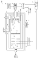
- FIG. 1 is an explanatory diagram schematically showing a configuration of a nanocluster generation apparatus 10 of the present embodiment.
- the nanocluster generator 10 includes a chamber 11 that is evacuated, a nanocluster growth cell 12 that is installed in the chamber, and a sputtering source 13 (magnetron sputtering source) that is installed in the nanocluster growth cell 12. .
- the nanocluster growth cell 12 of the present embodiment is surrounded by a liquid nitrogen jacket 14 so that liquid nitrogen (N 2 ) flows through the liquid nitrogen jacket 14.
- the nanocluster generation apparatus 10 further includes a control device 15 and a sputtering source pulse power supply 16 as components of the control system.
- the nanocluster generator 10 further includes a first inert gas supply pipe 17 for supplying a first inert gas (for example, argon gas (Ar)) for generating plasma to the sputtering source 13, and A second inert gas (for example, helium gas (He)) for cooling and aggregating neutral atoms and ions generated from the sputter source 13 and growing them as nanoclusters is supplied into the nanocluster growth cell 12.
- a first inert gas for example, argon gas (Ar)
- a second inert gas for example, helium gas (He)
- An inert gas supply pipe 18 is provided.
- the main part of the second inert gas supply pipe 18 is housed in the liquid nitrogen jacket 14, spirals around the inside of the liquid nitrogen jacket 14, and its end is inside the nanocluster growth cell 12. Protruding.
- the nanocluster generation device 10 further includes an exhaust device 19 composed of a turbo molecular pump or the like.
- the exhaust device 19 exhausts the chamber 11 to a predetermined degree of vacuum (for example, 10 ⁇ 1 to 10 ⁇ 4 Pa).
- the sputtering source 13 includes a target 131 (for example, a metal target), an anode 132, and a magnet unit 133.
- the target 131 is connected to the sputtering source pulse power source 16 as a cathode.
- Ar gas is supplied into the nanocluster growth cell 12 from the first inert gas supply pipe 17 and pulsed power is supplied from the pulse power source 16 for the sputtering source (that is, a high voltage is applied between the target 131 and the anode 132). Is applied in the form of pulses), a glow discharge is generated between the target 131 and the anode 132.
- the nanocluster generating apparatus 10 of the present embodiment can perform magnetron sputtering and generate a stronger glow discharge.
- the tip of the first inert gas supply pipe 17 is configured to inject the first inert gas from one or a plurality of locations between the target 131 and the anode 132 of the sputtering source 13. ing.
- the present invention is not limited to such a configuration, and any configuration can be adopted as long as the first inert gas can be supplied toward the target 131.
- the sputter source 13 is accommodated in the nanocluster growth cell 12 so as to be movable in the tube axis direction. This defines the stretching distance in the tube axis direction of the nanocluster growth region (growth region length, that is, the distance from the target 131 surface to the beam extraction port 121).
- the first inert gas is supplied to the sputtering source 13 in a state where the second inert gas cooled to the liquid nitrogen temperature is introduced into the nanocluster growth cell 12, and the sputtering source Pulse power is supplied from the pulse power supply 16 for use.
- pulsed power is supplied, sputtered particles such as neutral atoms and ions derived from the target 131 are discharged as a group from the target 131 into the second inert gas.
- This group is released at intervals of the repetition frequency of the pulse power applied to the sputtering source 13 and moves along the flow of the second inert gas. At this time, sputtered particles such as neutral atoms and ions constituting the group are combined with each other in the second inert gas to generate nanoclusters of various sizes.
- the generated nanocluster passes through the beam outlet 121 of the nanocluster growth cell 12 and then enters an ion detection device or the like at the subsequent stage.
- the ion detection apparatus 20 shown in FIG. 2 has an ion guide electrode 21 on the outer side in the vicinity of the beam extraction port 121 of the nanocluster growth cell 12, and thereby the nano discharge emitted from the beam extraction port 121 of the nanocluster growth cell 12.
- Guide cluster ions As shown in FIG. 2, the ion detector 20 includes a quadrupole ion deflector 22 provided on the beam extraction port side of the ion guide electrode 21. The quadrupole ion deflector 22 takes out by deflecting only one of positive ions or negative ions in the nanocluster.
- Nanocluster generation is performed by the nanocluster generation apparatus 10 having the above configuration.
- the following are the device specifications and experimental parameters for this example.
- Sputtering source Angstrom Sciences ONYX-2 Pulse power supply: Zpulser AXIA-150 Target: Ag (diameter 2 inches, purity 99.99%)
- Ar gas flow rate 40-200sccm
- He gas flow rate 60-600sccm
- Growth cell pressure 10-40Pa
- Growth cell inner diameter 110 mm
- Growth area length 190-290mm
- Beam extraction diameter 12 mm
- Nanocluster ions generated by the above settings were detected by the ion detector 20.
- the sputter source pulse power source 16 used in the present embodiment has a built-in pulse generator, and the supply voltage DCV from the power source 16 can be controlled from 80 V to 600 V. Accordingly, the peak voltage and the peak current are increased. fluctuate.
- the peak discharge power is represented by peak voltage ⁇ peak current.
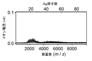
- FIG. 3 is an explanatory diagram for explaining the size distribution of Ag nanocluster positive ions generated by the nanocluster generator 10.
- the average discharge power of the pulse power supply 16 for the sputtering source is about 30 W, and the supply voltage DCV is 105 V.
- the mass spectrum when the repetition frequency of discharge is 70 Hz.
- the mass number per cluster (m / Z) is on the horizontal axis, and the ion current (pA) corresponding to the amount of cluster ions generated is on the vertical axis.
- FIG. 4 shows a mass spectrum (a) of Ag nanocluster negative ions obtained by a modulated pulse power magnetron sputtering method (hereinafter referred to as MPP-MSP method) using a modulated pulse power source, and a direct current magnetron sputtering method (DC-MSP).
- MPP-MSP method modulated pulse power magnetron sputtering method
- DC-MSP direct current magnetron sputtering method
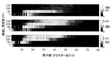
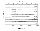
- FIG. 5 is a diagram showing that the ion intensity can be enhanced by controlling the parameters of the modulated pulse power source.
- FIG. 5 shows the ion intensities of Ag nanocluster negative ions when (a) the discharge power is 370 W, (b) the discharge power is 320 W, and (c) the discharge power is 210 W, respectively.
- the horizontal axis indicates the number of atoms per cluster, and the vertical axis indicates the pulse discharge repetition frequency.
- the color shades in the figure indicate that the lighter the color shade is (the closer it is to white), the higher the ionic strength.
- the generation duration of each pulse discharge is fixed (about 1 ms).
- the duty ratio of the pulse discharge is proportional to the repetition frequency (that is, the duty ratio is about 0.007 to 0.15 for the repetition frequency of 7 Hz to 150 Hz). It can be seen from FIG. 5 that the ion intensity (yield and yield) can be enhanced by two-dimensional control (optimization) of peak discharge power and discharge repetition frequency (or duty ratio).
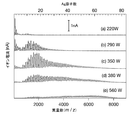
- FIG. 6 is an explanatory diagram for explaining the influence on the cluster size and ion intensity when the peak discharge power is changed in the MPP-MSP method.
- the peak discharge power is (a) 220 W and (b) 290 W, respectively. , (C) 350 W, (d) 380 W, and (e) Ag nanocluster negative ion size distributions when set to 560 W are offset.
- the Ar flow rate was 120 sccm
- the He flow rate was 600 sccm
- the discharge repetition frequency was 10 Hz. From FIG. 6, it can be read that the distribution of the cluster size changes depending on the peak discharge power, that is, the larger the peak discharge power, the larger the distribution of the cluster size tends to change.
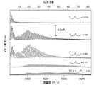
- FIG. 7 is an explanatory diagram for explaining the influence on the Ag nanocluster size and ion intensity when the duty ratio t ON / t TOT of the discharge is changed in the MPP-MSP method.
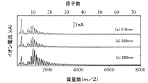
- FIG. 8 is an explanatory diagram for explaining the influence of the cluster growth region length on the Ag nanocluster size and the ionic strength, with (a) 210 mm, (b) 250 mm, and (c) 280 mm offset. It is a representation.
- the Ar gas flow rate is 80 sccm
- the He gas flow rate is 600 sccm
- the supply voltage DCV is 90 V
- the discharge repetition frequency is 70 Hz.
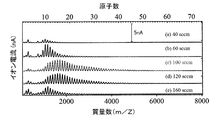
- FIG. 9 is an explanatory diagram for explaining the influence of the Ar gas flow rate on the Ag nanocluster size and ionic strength.
- the Ar gas flow rates are (a) 40 sccm, (b) 60 sccm, (c) 100 sccm, (d).
- the cluster size distributions at 120 sccm and (e) 160 sccm are respectively shown.
- the flow rate of He gas is 600 sccm
- the cluster growth region length is 290 mm
- the supply voltage DCV is 90 V
- the discharge repetition frequency is 70 Hz.
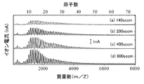
- FIG. 10 is an explanatory diagram for explaining the influence of the change in the He gas flow rate on the Ag nanocluster size and the ionic strength.
- the He gas flow rates are (a) 140 sccm, (b) 200 sccm, (c) 400 sccm, ( d)
- the cluster size distribution in the case of 600 sccm is represented by being offset.
- the Ar gas flow rate is 80 sccm
- the cluster growth region length is 290 mm
- the supply voltage DCV is 90 V
- the nanocluster generating apparatus 10 of the present embodiment uses the magnetron sputtering method that applies pulsed power, the size selectivity of the generated nanoclusters is better than the conventional DC power magnetron sputtering method. And the yield and yield are improved.
- the size selectivity of the generated nanoclusters can be improved.
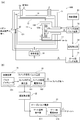
- the nanocluster generation apparatus 100 includes a beam extraction port 121 of the nanocluster growth cell 12 in addition to the configuration of the nanocluster generation apparatus 10 according to the first embodiment.
- a gate 30, a gate pulse power supply 31, and a delay generator 32 that allow or prohibit passage of nanocluster ions are provided.
- the gate 30 is, for example, a metal mesh electrode, and is installed in the vicinity of the beam extraction port 121 of the nanocluster growth cell 12 in the chamber 11. Only one nanocluster ion having one polarity among the nanocluster ions is allowed to pass therethrough. Or used to ban.
- the control system of the nanocluster generation apparatus 100 includes a control apparatus 15, a sputtering source pulse power supply 16, a delay generator 32, and a gate pulse power supply 31.
- the control device 15 has a pulse generator 151.
- the control device 15 may not be provided, and the pulse generator may be incorporated in the sputtering source pulse power supply 16.
- the sputter source pulse power supply 16 includes a sputter signal generator 161 and a sputter source power supply main body 162.
- the gate pulse power supply 31 includes a gate signal generator 311 and a gate power supply body 312.
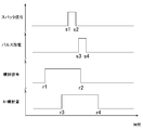
- the pulse generator 151 When generating a cluster, the pulse generator 151 generates a pulsed clock signal and sends it to the sputter signal generator 161 of the sputter source pulse power supply 16.
- the sputter signal generator 161 When the sputter signal generator 161 receives the clock signal, the sputter signal generator 161 generates a pulsed sputter signal, sends the sputter signal to the power source main body 162 for the sputter source, and sends a synchronization signal to the delay generator 32.
- the power source main body 162 for the sputtering source applies a pulsed high voltage to the sputtering source 13 while the sputtering signal is on.
- the delay generator 32 When the delay generator 32 receives the synchronization signal, the delay generator 32 generates a delay signal having a predetermined delay with reference to the synchronization signal, and sends the delay signal to the gate pulse power supply 31.
- the gate signal generator 311 of the gate pulse power supply 31 receives the delay signal, generates a pulsed gate signal, and sends it to the gate power supply body 312.
- the gate power supply body 312 applies a voltage to the gate according to the gate signal. For example, the gate power supply body 312 applies a positive or negative voltage to the gate only while the gate signal is off.
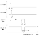
- the sputter signal generator 161 sends a synchronization signal to the delay generator 32 at time s1.
- the delay generator 32 generates a delay signal having a predetermined delay with reference to the received synchronization signal, and sends the delay signal to the gate pulse power supply 31.
- the gate signal generator 311 of the gate pulse power supply 31 Upon receiving the delay signal, the gate signal generator 311 of the gate pulse power supply 31 generates a pulsed gate signal (t1 to t2) and sends it to the gate power supply body 312.
- the gate power supply body 312 applies a voltage to the gate according to the gate signal. In this example, the positive voltage + V is applied to the gate only while the gate signal is off, and the voltage applied to the gate is 0 V only while the gate signal is on.
- the positive cluster ions emitted from the beam extraction port 121 of the cluster growth cell 12 are bounced back to the gate 30 and cannot pass through the gate 30. Only when the potential of the gate 30 is 0 V, the positive cluster ions can pass through the gate 30 and can enter the ion detection device or the like at the subsequent stage.
- the time frame (t1 to t2) in which the potential of the gate 30 is set to 0V and the passage of the cluster ions having the code to be permitted / not permitted to pass is referred to as a passage permission window.
- FIG. 13 the distribution of the size of cluster ions at each elapsed time from the time s1 when the sputtering signal rises is plotted, and in order from the bottom, 0 ms, 40 ms, 50 ms, 60 ms, 70 ms, 90 ms, 100 ms, 140 ms. It represents the one at the time.
- the size distribution of detected cluster ions changes as time elapses after the sputter signal is generated and the pulse discharge starts, that is, the cluster size has a time distribution.
- the cluster growth region length is 290 mm
- the supply voltage is 120 V
- the repetition frequency is 7 Hz
- the passage permission window is 4 ms.
- the ion current near the mass number of 4000 is high in the range of 50 ms to 70 ms, once decreases at 90 ms, and increases again at 100 ms. From this, it can be seen that even if the clusters have the same size, there are those having different flight times.
- the difference in flight time between clusters of the same size can be attributed to the difference in mobility. That is, it is suggested that clusters having the same size and different structures (structural isomers) reach the gate 30 and are taken out at different time zones.
- FIG. 14A plots the amount of ions detected at each time in one pulse discharge cycle with a black circle on the vertical axis, with the elapsed time from when the sputtering signal is generated as the horizontal axis.
- the curve is an approximate curve. As shown in the figure, when a sputter signal is generated at time 0 and a discharge is generated immediately after that, after the flight time elapses until the cluster ions fly through the cluster growth cell 12 and reach the gate 30 first, Ions begin to be detected.
- a nanocluster beam whose size distribution is controlled with high accuracy can be obtained. Is possible. By repeating the same operation every repetition period, the yield of the nanocluster beam whose size distribution is controlled with high accuracy can be increased.
- the gate 30 is a metal mesh, but the present invention is not limited to this. That is, if the device can permit or prohibit the passage of cluster ions using an electric field, a magnetic field, or an electromagnetic field, or change the flight trajectory (for example, a deflector, a Wien filter, etc.), it can be used as the gate 30. Is possible. Furthermore, if the neutral cluster is ionized by laser irradiation, electron beam irradiation, or the like, it is possible to permit / prohibit the passage of the neutral cluster-derived cluster ions by the gate 30.
- a device for example, a shutter
- a mechanical device such as a device that physically changes the flight path (for example, a gas injection valve that can inject gas in a pulsed manner) or a disk that has a predetermined slit and can rotate at high speed is used as the gate 30. It may be used instead of. In this case, it can be used as a gate for both neutral clusters and cluster ions.
- the nanocluster generation apparatus 200 of this embodiment is characterized in that a gate is also provided inside the cluster growth cell 12. That is, as shown in FIG. 15, the gate includes a first gate 40 installed inside the cluster ion growth cell 12 and a second gate 50 installed near the beam extraction port 121 of the cluster growth cell 12. Further, a first gate pulse power supply 41 and a second gate pulse power supply 51 are provided. Furthermore, in order to avoid that the voltage applied to the first gate 40 affects the upstream and downstream electric fields, a metal ground member 42 (for example, a metal mesh) covering the first gate 40 is provided. I have. The potential of the ground member 42 is the same as that of the cluster growth cell 12. The first gate 40 extends near the center of the internal space of the cluster growth cell 12.
- the internal space of the cluster growth cell 12 is partitioned by the first gate 40 into an upstream region and a downstream region.
- the cluster ions grown in the upstream region pass through the first gate 40, and are permitted or prohibited. be able to. That is, by setting a predetermined passage permission window for the first gate 40, only cluster ions having a specific size distribution can be selectively passed through the first gate 40 for positive or negative cluster ions. .
- the region inside the cluster growth cell 12 and downstream of the first gate 40 is configured as a region for controlling the flight trajectory and flight speed of the nanocluster ions that have passed through the first gate 40.
- FIG. 15 shows that a plurality of ion motion control electrodes 60 installed in the cluster growth cell 12 accelerate or decelerate the passing cluster ions and change their flight paths, thereby By utilizing the difference in mass and mobility, the cluster ion growth is promoted and suppressed, and the size and structure are selectively controlled.
- the ion motion control electrode 60 is controlled by voltage application by the ion motion controller 61, and the ion motion controller 61 is controlled by a control signal generated from the delay generator 32 in synchronization with the sputtering signal.
- the method for controlling the flight trajectory and flight speed of nanocluster ions is not limited to this, and any configuration may be used as long as the flight trajectory and flight speed of cluster ions can be controlled.
- generation apparatus 300 which concerns on 4th Embodiment of this invention is demonstrated.
- the nanocluster generating apparatus 300 injects Ar gas as the first inert gas in addition to the configuration of the nanocluster generating apparatus 10 of the first embodiment.
- a valve 70 and an injection valve pulse power supply 71 for controlling the operation of the injection valve 70 are provided. Thereby, it is possible to inject Ar gas in pulses. That is, the injection valve 70 is installed outside the chamber 11, and is supplied with pulsed power from the injection valve pulse power supply 71, whereby Ar gas is intermittently supplied via the first inert gas supply pipe 17. Can be jetted.
- Ar gas injected from the opening of the inert gas supply pipe 17 is jetted substantially in parallel with the target 131 from one or a plurality of locations on the inner peripheral surface of the anode 132 in the vicinity of the sputtering surface of the target 131. Spread with an angle.
- Ar gas is supplied to the injection valve 70 from a high-pressure gas supply device (not shown).
- the high pressure gas supply device includes, for example, an Ar gas tank that stores Ar gas, a pressure regulator, and the like.
- injection valve 70 for example, an automobile fuel injection valve (for example, an injector for a diesel engine) can be used.
- the classification based on the valve drive system may be an electromagnetic valve or a piezo valve, and any type of injection valve can be used as long as the drive described below can be performed.
- the control system of the pulse sputtering device 300 includes a control device 15, a sputtering source pulse power supply 16, a delay generator 32, a gate pulse power supply 31, and an injection valve pulse power supply 71.
- the injection valve pulse power supply 71 includes an injection signal generator 711 and an injection valve power supply body 712. Other configurations are the same as those of the second embodiment.
- the pulse generator 151 generates a pulsed clock signal and sends it to the delay generator 32.
- the delay generator 32 is a multi-channel delay device, and includes a first delay signal having a first delay based on a clock signal, a second delay signal having a second delay different from the first delay, and A third delay signal having a different third delay is generated. Then, the first delay signal is sent to the sputter source pulse power source 16, the second delay signal is sent to the injection valve pulse power source 71, and the third delay signal is sent to the gate pulse power source 31.
- the sputter signal generator 161 of the sputter source pulse power source 16 Upon receipt of the first delay signal, the sputter signal generator 161 of the sputter source pulse power source 16 generates a pulsed sputter signal and sends it to the sputter source power source body 162.
- the power source main body 162 for the sputtering source applies a pulsed high voltage to the sputtering source 13 while the sputtering signal is on.
- the injection signal generator 711 of the injection valve pulse power supply 71 Upon receiving the second delay signal, the injection signal generator 711 of the injection valve pulse power supply 71 generates a pulsed injection signal and sends it to the injection valve power supply body 712.
- the injection valve power supply main body 712 supplies pulsed power to the injection valve 70 according to the injection signal (for example, a voltage is applied to the injection valve 70 while the injection signal is on).
- Ar gas is supplied from the injection valve 70 to the vicinity of the sputtering surface of the target 131, and pulse discharge is generated at the sputtering source 13, so that sputtered particles are released from the target 131.
- the operation of the gate 30 is included and is the same as in the second embodiment.
- the control of the sputter source pulse power supply 16 and the gate pulse power supply 31 is substantially the same as that shown in FIG. 12 although two delay signals are used in this embodiment.
- the delay generator 32 appropriately controls the sputter signal transmission start time s1 and the injection signal transmission start time r1 by the first and second delay signals, and the sputter signal generator 161 transmits the sputter signal.
- the end time s2 or the sputter signal duration
- the injection signal generator 711 appropriately controlling the injection signal transmission end time r2 (or the injection signal duration)
- pulse discharge is actually performed.
- the whole of the periods s3 to s4 occurring in step S3 is included in the periods r3 to r4 in which Ar gas is actually injected.
- the supply amount of Ar gas is greatly reduced as compared with the case of continuously supplying Ar gas, but the period when Ar gas is actually used, that is, immediately before the period when pulse discharge occurs. In the period from to immediately after, a necessary amount of Ar gas can be reliably supplied.
- a predetermined delay time is set from time r3 when Ar gas injection is actually started to time s3 when pulse discharge is actually started. Is preferred. Thereby, pulse discharge can be generated in a state where a sufficient amount of Ar gas for sputtering is supplied to the target 131.
- a predetermined delay time from time s4 when the actual pulse discharge ends to time r4 when the actual Ar gas injection ends is set.
- the injection of Ar gas can be continued until the completion of sputtering.
- the duty ratio of the injection valve 70 (that is, the injection valve 70 is actually used). Is preferably 50% or less.
- the tip of the first inert gas supply pipe 17 is configured to inject the first inert gas from one or a plurality of locations between the target 131 and the anode 132 of the sputtering source 13. ing.
- the configuration is not limited to such a configuration, and any configuration can be adopted as long as the first inert gas can be supplied so that the first inert gas is directed toward the target 131.
- the injection valve 70 may be installed inside the chamber 11, inside the cluster growth cell 12, or inside the sputtering source 13.
- the sputter signal generated by the sputter signal generator 161 of the sputter source pulse power supply 16 is a single pulse signal (see FIG. 12).
- the sputter signal may be emitted as a signal group consisting of a plurality of micropulse signals.
- a method of configuring the sputter signal generator 161 with a micro pulse generator is conceivable.
- One example is the use of a modulated pulse power supply.
- the pulse width of each micro pulse signal is, for example, about 10 microseconds, and a plurality of the pulse widths are successively emitted, whereby a sputter signal is emitted as a signal group covering a period of about 100 microseconds to 3 milliseconds as a whole.
- the sputtering source power supply main body 162 supplies power to the sputtering source 13 in accordance with the received sputtering signal.
- the electric power supplied can be made variable during the discharge period for each cycle by controlling each micro pulse signal.
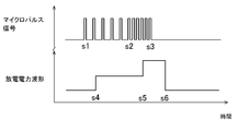
- the frequency of the micro pulse signal is relatively low in the periods s1 to s2 (that is, the micro pulse signal group is sparse), and the frequency of the micro pulse signal in the periods s2 to s3 is relatively high. (That is, the micropulse signal group is dense).
- the power supplied to the sputtering source 13 has a relatively small value in the period s4 to s5 in the initial period of power application, and thereafter has a relatively large value in the period s5 to s6 until the end of the application. .
- the frequency of the micro pulse signal is not limited to variable, or in addition, the duty ratio of the micro pulse signal may be variable. Further, the voltage value of the power source main body 162 for the sputtering source may be changed. Further, the injection signal generator 711 may also be configured by a micro pulse generator, like the sputtering signal generator 161.
- the sputter source 13 is installed in the cluster growth cell 12, but the present invention is not limited to this. That is, as long as the sputter source 13 is in the chamber 11 and the sputtered particles ejected from the target 131 of the sputter source 13 can immediately enter the cluster growth cell 12 immediately after that, the sputter source 13 is in the cluster. It may be arranged outside the growth cell 12.
- the cooling jacket 14 made of liquid nitrogen is used.
- the present invention is not limited to this.
- the configuration of the control system described in each of the above embodiments is merely an example, and any control system can be used as long as it can perform the same control as each control described above.
- Such a system configuration may be adopted.
- the clock signal from the pulse generator 151 in FIG. 11B can be directly sent to the delay generator 32.
- FIG. 19 is a diagram showing the change over time of the generation intensity of TaSi composite nanocluster positive ions.
- the experimental conditions are as follows.
- the right vertical axis represents the delay ⁇ t shown in FIG.
- the horizontal axis represents the size (mass number) of the detected nanocluster.
- the vertical axis on the left indicates the detected intensity (arbitrary unit) of the nanocluster.
- Each mass spectrum is measured by changing the delay ⁇ t by 10 ms, and the delay ⁇ t increases toward the upper side of the figure. As shown in FIG.
- the strength of TaSi 16 + (m 630 a.m.u.), which is particularly stable among TaSi composite nanoclusters, is maximum in the region of 100 to 120 ms.
- the nanocluster generation method using the nanocluster generation apparatus according to the present invention can be applied to a non-metallic target, and the method can be applied to a composite binary system.
Landscapes
- Chemical & Material Sciences (AREA)
- Engineering & Computer Science (AREA)
- Analytical Chemistry (AREA)
- Physics & Mathematics (AREA)
- Plasma & Fusion (AREA)
- Chemical Kinetics & Catalysis (AREA)
- Materials Engineering (AREA)
- Mechanical Engineering (AREA)
- Metallurgy (AREA)
- Organic Chemistry (AREA)
- Physical Vapour Deposition (AREA)
Abstract
【課題】 ナノクラスター生成装置において、ナノクラスターのサイズ制御及び構造制御を向上させる。また、サイズ及び構造の少なくとも一方が選択されたナノクラスターの収量および収率を増大させる。 【解決手段】 ナノクラスター生成装置は、真空容器と、パルス放電を行い、プラズマを発生させるスパッタ源と、スパッタ源に対し、パルス状の電力を供給するパルス電源と、スパッタ源に対し第1の不活性ガスを供給する第1不活性ガス供給装置と、真空容器内に収容されるナノクラスター成長セルと、ナノクラスター成長セル内に第2の不活性ガスを導入する第2不活性ガス導入装置と、を備える。
Description
本発明は、ナノクラスター生成装置に関する。
ナノクラスターは、原子一個の増減による性質の変化が著しいことから、ナノクラスター生成において、ナノクラスターを構成する原子数(以下、クラスターサイズという)の分布を制御したナノクラスタービームの手法開発が課題となっている。
直流電源を利用したマグネトロンスパッタリング法(以下DC-MSP法)を用いたナノクラスター源の開発によって上記課題は相対的に向上、改善されている。例えば、非特許文献1のものは、主としてHe分圧を制御することにより、クラスターサイズを制御し得るという可能性を示唆するものである(非特許文献1の図4参照)。また、非特許文献2においては、Heガス用ノズルの形状がクラスターサイズに与える影響についての記載がある(非特許文献2の図4参照)。
しかしながら、サイズ分布制御が困難であることや、サイズ選択されたナノクラスターイオンビームの強度が数十pA(0.6~3×10⁸個/秒)以下と微弱であることから、ナノクラスターの生成量が少ないといった課題については依然として解決が求められている。
その他、関連する文献として、特許文献1~3や非特許文献3~5も参照されたい。
"Size-selected cluster beam source based on radio frequency magnetron plasma sputtering and gas condensation", S. Pratontep, S. J. Carroll, C. Xirouchaki, M. Streun, R. E. Palmer, Rev. Sci. Instrum. 76, 045103 (2005)
"Chemical reactivity of size-selected supported clusters: An experimental setup", U. Heiz, F. Vanolli, L. Trento, W.-D. Schneider, Rev. Sci. Instrum. 68, 1986-1994 (1997)
"Size-controlled formation of Cu nanoclusters in pulsed magnetron sputtering system", STRANAK Vitezslav, BLOCK Stephan, DRACHE Steffen, HUBICKA Zdenek, HELM Christiane A., JASTRABIK Lubomir, TICHY Milan, HIPPLER Rainer, Surf. Coat. Technol., Vol.205, No.8-9, Page.2755-2762 (2011.01.25)
"Deposition of size-selected metal clusters generated by magnetron sputtering and gas condensation: a progress review", XIROUCHAKI C, PALMER R E (Univ. Birmingham, Birmingham, GBR), Phil. Trans. R. Soc. Lond. A, Vol.362, No.1814, Page.117-124 (2004.01.15)
"Ion energy and mass distribution of the plasma during modulated pulse power magnetron sputtering", J. Lin, J.J. Moore, W.D. Sproul, B. Mishra, J.A. Rees, Z. Wu, R. Chistyakov, B. Abraham, Surf. Coat. Technol., Volume 203, Issue 24, 15 September 2009, Page.3676-3685
そこで、本発明の目的の一つは、ナノクラスター生成装置において、ナノクラスターのサイズ制御及び構造制御を向上させることにある。また、本発明のもう一つの目的は、ナノクラスターの生成効率を向上させることにより、サイズ及び構造の少なくとも一方が選択されたナノクラスターの収量および収率を増大させることにある。
本発明の第1の局面によるナノクラスター生成装置は、
真空容器と、
パルス放電を行い、プラズマを発生させるスパッタ源と、
スパッタ源に対し、パルス状の電力を供給するパルス電源と、
スパッタ源に対し、第1の不活性ガスを供給する第1不活性ガス供給装置と、
真空容器内に収容されるナノクラスター成長セルと、
ナノクラスター成長セル内に第2の不活性ガスを導入する第2不活性ガス導入装置と、を備えるナノクラスター生成装置である。
真空容器と、
パルス放電を行い、プラズマを発生させるスパッタ源と、
スパッタ源に対し、パルス状の電力を供給するパルス電源と、
スパッタ源に対し、第1の不活性ガスを供給する第1不活性ガス供給装置と、
真空容器内に収容されるナノクラスター成長セルと、
ナノクラスター成長セル内に第2の不活性ガスを導入する第2不活性ガス導入装置と、を備えるナノクラスター生成装置である。
上記構成によれば、スパッタ源に対し、パルス状の電力を供給することにより、DC-MSP法の場合と比べて、非常に高いピーク出力の下においても安定な放電が維持でき、実効的な平均出力を高めることができる。これにより、クラスターの生成量を増大させることができる。また、クラスターのサイズ及び構造の選択性が向上する。
本発明の第2の局面によれば、上記のナノクラスター生成装置は、パルス状の電力のデューティ比およびピーク放電電力を可変とするようにパルス電源を制御する制御装置、を更に備える。このような制御装置を用いてパルス状の電力のデューティ比とピーク放電電力を最適化することにより、クラスター生成量を極大化することが可能となる。また、クラスターのサイズ及び構造の選択性が向上する。
本発明の第3の局面によれば、上記のナノクラスター生成装置において、スパッタ源は、カソードとしてのターゲットを有し、
ターゲットのスパッタ面と、ナノクラスター成長セルの内側面は、ナノクラスターを成長させるためのナノクラスター成長空間を規定し、
制御装置は、ターゲットのスパッタ面からのナノクラスター成長空間の延伸距離、ナノクラスター成長セル内の第2不活性ガスの温度および圧力の少なくとも一つに応じて、パルス状の電力のデューティ比及びピーク放電電力の少なくとも一方を可変とする。
このような構成により、装置構成やクラスター生成条件に応じて、パルス状の電力のデューティ比やピーク放電電力を最適化することができる。
ターゲットのスパッタ面と、ナノクラスター成長セルの内側面は、ナノクラスターを成長させるためのナノクラスター成長空間を規定し、
制御装置は、ターゲットのスパッタ面からのナノクラスター成長空間の延伸距離、ナノクラスター成長セル内の第2不活性ガスの温度および圧力の少なくとも一つに応じて、パルス状の電力のデューティ比及びピーク放電電力の少なくとも一方を可変とする。
このような構成により、装置構成やクラスター生成条件に応じて、パルス状の電力のデューティ比やピーク放電電力を最適化することができる。
本発明の第4の局面によれば、上記のナノクラスター生成装置において、制御装置は、パルス状の電力の繰り返し周波数を可変とするようにパルス電源を制御する。このような制御装置を用いてパルス状の電力の繰り返し周波数を最適化することにより、クラスター生成量を極大化することが可能となる。また、クラスターのサイズ及び構造の選択性が向上する。
本発明の第5の局面によれば、上記のナノクラスター生成装置において、スパッタ源は、カソードとしてのターゲットを有し、
ターゲットのスパッタ面と、ナノクラスター成長セルの内側面は、ナノクラスターが成長するナノクラスター成長空間を規定し、
制御装置は、ターゲットのスパッタ面からのナノクラスター成長空間の延伸距離、ナノクラスター成長セル内の第2不活性ガスの温度および圧力の少なくとも一つに応じて、パルス状の電力の繰り返し周波数を可変とする。
このような構成により、装置構成やクラスター生成条件に応じて、パルス状の電力の繰り返し周波数を最適化することができる。
ターゲットのスパッタ面と、ナノクラスター成長セルの内側面は、ナノクラスターが成長するナノクラスター成長空間を規定し、
制御装置は、ターゲットのスパッタ面からのナノクラスター成長空間の延伸距離、ナノクラスター成長セル内の第2不活性ガスの温度および圧力の少なくとも一つに応じて、パルス状の電力の繰り返し周波数を可変とする。
このような構成により、装置構成やクラスター生成条件に応じて、パルス状の電力の繰り返し周波数を最適化することができる。
本発明の第6の局面によれば、上記のナノクラスター生成装置において、真空容器はナノクラスター成長セル内で生成したナノクラスターをビームとして取り出すためのビーム取り出し口を有し、
ナノクラスター生成装置は更に、ビーム取り出し口からのビームの取り出しを許可または禁止のいずれかとするゲートを備え、
制御装置は、スパッタ源に対するパルス状の電力の供給を開始するタイミングを基準として、ゲートによるビーム取り出し口からのイオンビームの取り出しの許可と禁止とを切り替えるタイミングを設定する。
このような構成によれば、ゲートを操作して特定の時間帯にビーム取出し口に到達するビームのみを選択的に取り出すことができ、例えば、特定のサイズ又は構造を有するクラスターの堆積を行うことができる。
ナノクラスター生成装置は更に、ビーム取り出し口からのビームの取り出しを許可または禁止のいずれかとするゲートを備え、
制御装置は、スパッタ源に対するパルス状の電力の供給を開始するタイミングを基準として、ゲートによるビーム取り出し口からのイオンビームの取り出しの許可と禁止とを切り替えるタイミングを設定する。
このような構成によれば、ゲートを操作して特定の時間帯にビーム取出し口に到達するビームのみを選択的に取り出すことができ、例えば、特定のサイズ又は構造を有するクラスターの堆積を行うことができる。
本発明の第7の局面によれば、上記のナノクラスター生成装置において、制御装置は、ビーム取り出し口からのビームの取り出しを許可する期間と禁止する期間とを、パルス状放電と同期した一定のパターンとして設定し、該設定したパターンに従って、パルス状の電力の繰り返し周期と同期させてビーム取り出し口からのビームの取り出しの許可と禁止とを繰り返す。
このような構成によれば、パルス状の電力の繰り返し周期と同期した所定の時間帯にビーム取出し口に到達するビームのみを繰り返し取り出すことができ、これにより、特定の性質を有するクラスターイオンの収量及び収率を向上させることが可能となる。なお、例えば、収率とは、スパッタ源のターゲットからクラスター成長セル内に供給されるスパッタ放出粒子の総量に対する、所望のクラスターの生成量の割合として定義することができる。
このような構成によれば、パルス状の電力の繰り返し周期と同期した所定の時間帯にビーム取出し口に到達するビームのみを繰り返し取り出すことができ、これにより、特定の性質を有するクラスターイオンの収量及び収率を向上させることが可能となる。なお、例えば、収率とは、スパッタ源のターゲットからクラスター成長セル内に供給されるスパッタ放出粒子の総量に対する、所望のクラスターの生成量の割合として定義することができる。
本発明の第8の局面によれば、上記のナノクラスター生成装置において、制御装置は、ビームの取り出しの許可と禁止とを切り替えるタイミングを可変とすることで、ビーム取り出し口を介して取り出されるナノクラスターのサイズ及び構造の少なくとも一方を制御する。
パルス状の電力の繰り返し周期内において発生するナノクラスターのサイズや構造が時間分布を有している場合、上記構成によれば、ビーム取り出し口を介して取り出されるナノクラスターのサイズや構造を制御することが可能となる。
パルス状の電力の繰り返し周期内において発生するナノクラスターのサイズや構造が時間分布を有している場合、上記構成によれば、ビーム取り出し口を介して取り出されるナノクラスターのサイズや構造を制御することが可能となる。
本発明の第9の局面によれば、上記のナノクラスター生成装置において、ゲートは、電場、磁場、または電磁場により、ビーム取り出し口からのビームの取り出しを許可又は禁止する。このような構成によれば、上記したような作用を持つゲートを提供することができる。
本発明の第10の局面によれば、上記のナノクラスター生成装置において、ゲートは、ビームの飛行経路を変更し、遮断し、又は、開放することにより、ビーム取り出し口からのビームの取り出しを禁止し、又は、許可する。このような構成によっても、上記したような作用を持つゲートを提供することができる。
本発明の第10の局面によれば、上記のナノクラスター生成装置において、ゲートは、ビームの飛行経路を変更し、遮断し、又は、開放することにより、ビーム取り出し口からのビームの取り出しを禁止し、又は、許可する。このような構成によっても、上記したような作用を持つゲートを提供することができる。
本発明の第11の局面によれば、上記のナノクラスター生成装置は、クラスター成長セルの内部に設置され、ナノクラスターの通過を許可し、又は禁止する別のゲートを更に備える。
このような構成によれば、クラスター成長セル内部においてゲートにより選別したクラスターを対象として、更にクラスター成長セル内部において成長させたり、あるいは、加速や減速等の制御をしたりすることが可能となる。
このような構成によれば、クラスター成長セル内部においてゲートにより選別したクラスターを対象として、更にクラスター成長セル内部において成長させたり、あるいは、加速や減速等の制御をしたりすることが可能となる。
本発明の第12の局面によれば、上記のナノクラスター生成装置において、第1の不活性ガスはアルゴンガスである。
これによれば、アルゴンガスに基づくプラズマを発生させることができる。
これによれば、アルゴンガスに基づくプラズマを発生させることができる。
本発明の第13の局面によれば、上記のナノクラスター生成装置において、第2の不活性ガスはヘリウムガスである。
この場合、ヘリウムガスを冷媒として用いることで、スパッタ源からの放出粒子を冷却・凝集し、ナノクラスターへと成長させることができる。
この場合、ヘリウムガスを冷媒として用いることで、スパッタ源からの放出粒子を冷却・凝集し、ナノクラスターへと成長させることができる。
本発明の第14の局面によれば、上記のナノクラスター生成装置において、第1不活性ガス供給装置は、第1不活性ガスを噴射するガス噴射弁を有し、
制御装置は、ガス噴射弁が間欠的に第1不活性ガスを噴射するように、かつ、スパッタ源においてパルス放電が発生する期間が、ガス噴射弁により第1不活性ガスを噴射する期間内に含まれるように、スパッタ源及びガス噴射弁を制御する。
このような構成によれば、噴射弁を用いて第1不活性ガスを間欠的に噴射供給するため、第1不活性ガスを連続的に供給する場合に比べてその使用量を削減することができる。結果として、第1不活性ガスを供給・排出するための装置の小型化を図ることができる。更に上記局面によれば、制御装置は、スパッタ源においてパルス放電が発生する期間が、噴射弁により第1不活性ガスを噴射し供給する期間内に含まれるように、スパッタ源及び噴射弁を制御する。このことにより、第1不活性ガスの噴射による供給が間欠的なものであっても、パルス放電が行われるタイミングにおいては、スパッタ源に対して十分な量の第1不活性ガスが供給されるものとすることができる。これにより、第1不活性ガスに基づくプラズマの発生を確実なものとすることができる。
更には、ヘリウム等の第2不活性ガスの分圧を高く維持することができるため、安定したスパッタリングを行いながら、クラスターの冷却効率を向上させることができる。
本発明の第15の局面によれば、上記ナノクラスター生成装置において、制御装置は、パルス状の電気信号である噴射信号に応じて、ガス噴射弁に電力を供給することにより、ガス噴射弁を駆動して第1不活性ガスを噴射させ、
制御装置は、噴射信号を、複数のパルス信号群により構成し、かつ、噴射信号を構成するパルス信号群における複数のパルス信号のデューティ比又は周波数を可変とする。
このような構成により、第1不活性ガスの時間当たりの噴射量(即ち噴射率)を、1噴射期間中に変化させることができる。
制御装置は、噴射信号を、複数のパルス信号群により構成し、かつ、噴射信号を構成するパルス信号群における複数のパルス信号のデューティ比又は周波数を可変とする。
このような構成により、第1不活性ガスの時間当たりの噴射量(即ち噴射率)を、1噴射期間中に変化させることができる。
本発明の第16の局面によれば、上記のナノクラスター生成装置において、制御装置は、パルス状の電気信号であるスパッタ信号に応じて、スパッタ源に対してパルス状の電力を供給し、
制御装置は、電気信号を、複数のパルス信号群により構成し、かつ、電気信号を構成するパルス信号群における複数のパルス信号のデューティ比又は周波数を可変とする。
このような構成によれば、スパッタ源に対してパルス状の電力を供給する態様を任意に変化させることができ、ナノクラスター生成量を向上させる等の目的に応じたより好ましい放電態様を実現することができる。
制御装置は、電気信号を、複数のパルス信号群により構成し、かつ、電気信号を構成するパルス信号群における複数のパルス信号のデューティ比又は周波数を可変とする。
このような構成によれば、スパッタ源に対してパルス状の電力を供給する態様を任意に変化させることができ、ナノクラスター生成量を向上させる等の目的に応じたより好ましい放電態様を実現することができる。
(第1実施形態)
以下、本発明の第1実施形態によるナノクラスター生成装置10について説明する。図1は本実施形態のナノクラスター生成装置10の構成を概略的に示す説明図である。ナノクラスター生成装置10は、真空引きされるチャンバ11と、該チャンバ内に設置されるナノクラスター成長セル12と、該ナノクラスター成長セル12内に設置されるスパッタ源13(マグネトロンスパッタ源)を備える。本実施形態のナノクラスター成長セル12は、その周囲を液体窒素ジャケット14で囲まれており、該液体窒素ジャケット14内を液体窒素(N2)が流通するように構成されている。ナノクラスター生成装置10は更に、制御システムの構成要素として、制御装置15、スパッタ源用パルス電源16を備える。
以下、本発明の第1実施形態によるナノクラスター生成装置10について説明する。図1は本実施形態のナノクラスター生成装置10の構成を概略的に示す説明図である。ナノクラスター生成装置10は、真空引きされるチャンバ11と、該チャンバ内に設置されるナノクラスター成長セル12と、該ナノクラスター成長セル12内に設置されるスパッタ源13(マグネトロンスパッタ源)を備える。本実施形態のナノクラスター成長セル12は、その周囲を液体窒素ジャケット14で囲まれており、該液体窒素ジャケット14内を液体窒素(N2)が流通するように構成されている。ナノクラスター生成装置10は更に、制御システムの構成要素として、制御装置15、スパッタ源用パルス電源16を備える。
ナノクラスター生成装置10は更に、プラズマを発生させるための第1不活性ガス(例えば、アルゴンガス(Ar))をスパッタ源13に対して供給するための第1不活性ガス供給パイプ17、および、スパッタ源13から発生した中性原子やイオンを冷却し凝集させ、ナノクラスターとして成長させるための第2不活性ガス(例えばヘリウムガス(He))をナノクラスター成長セル12内へ供給するための第2不活性ガス供給パイプ18を備える。第2不活性ガス供給パイプ18は、その主要部が、液体窒素ジャケット14内に格納され、液体窒素ジャケット14の内部を螺旋状に周回して、その端部が、ナノクラスター成長セル12の内側に突出している。
こうして、液体窒素により冷却されたヘリウム等の第2不活性ガスをナノクラスター成長セル12内に導入することができる。クラスター成長セル12内の圧力が約2~40Paに維持されるようにする(圧力制御のためにクラスター成長セル12に備えられる圧力計、ガス供給系に備えられるマスフローコントローラ等の装置については、図示を省略している。)
ナノクラスター生成装置10は更にターボ分子ポンプ等からなる排気装置19を備え、この排気装置19により、チャンバ11内が所定の真空度(例えば10-1~10-4Pa)まで排気される。
ナノクラスター生成装置10は更にターボ分子ポンプ等からなる排気装置19を備え、この排気装置19により、チャンバ11内が所定の真空度(例えば10-1~10-4Pa)まで排気される。
スパッタ源13はターゲット131(例えば、金属ターゲット)、アノード132、磁石ユニット133から構成され、ターゲット131はカソードとしてスパッタ源用パルス電源16に接続される。第1不活性ガス供給パイプ17からナノクラスター成長セル12内にArガスが供給され、スパッタ源用パルス電源16からパルス状の電力が供給される(即ち、ターゲット131とアノード132の間に高電圧がパルス状に印加される)ことにより、ターゲット131及びアノード132間にグロー放電が生じる。また、磁石ユニット133によりターゲット131の表面付近に磁場を印加することで、本実施形態のナノクラスター生成装置10はマグネトロンスパッタを行い、さらに強いグロー放電を生成することが可能である。
本実施形態においては、第1不活性ガス供給パイプ17の先端は、第1不活性ガスをスパッタ源13のターゲット131とアノード132との間の一箇所または複数の箇所から噴射するように構成されている。ただし、このような構成に限らず、第1不活性ガスを、ターゲット131に向かうように供給できる構成である限り、任意の構成を採用可能である。
スパッタ源13は、ナノクラスター成長セル12内に、管軸方向に移動自在に収容される。これにより、ナノクラスター成長領域の管軸方向の延伸距離(成長領域長、すなわち、ターゲット131面からビーム取出し口121までの距離)を規定する。
スパッタ源13は、ナノクラスター成長セル12内に、管軸方向に移動自在に収容される。これにより、ナノクラスター成長領域の管軸方向の延伸距離(成長領域長、すなわち、ターゲット131面からビーム取出し口121までの距離)を規定する。
ナノクラスターを生成するためには、液体窒素温度に冷却された第2不活性ガスをナノクラスター成長セル12内に導入した状態で、スパッタ源13に第1不活性ガスを供給するとともに、スパッタ源用パルス電源16からパルス電力を供給する。パルス電力が供給されると、ターゲット131から第2不活性ガス中に、ターゲット131由来の中性原子及びイオン等のスパッタ粒子が集団として放出される。
この集団は、スパッタ源13に印加されるパルス電力の繰り返し周波数の間隔で放出されて第2不活性ガスの流れに沿って移動する。この時、集団を構成する中性の原子及びイオン等のスパッタ粒子は第2不活性ガス中において互いに結合して種々のサイズのナノクラスターを生成する。生成したナノクラスターはナノクラスター成長セル12のビーム取出し口121を通過した後、後段のイオン検出装置等へ進入する。
イオン検出装置として、例えば図2に示す構成のものを用いることができる。図2に示すイオン検出装置20は、ナノクラスター成長セル12のビーム取出し口121の近傍外側にイオンガイド電極21を有し、これにより、ナノクラスター成長セル12のビーム取出し口121から放出されるナノクラスターイオンをガイドする。図2に示すように、イオン検出装置20は、イオンガイド電極21のビーム取出し口側に設けられる四重極型イオン偏向器22を備える。四重極型イオン偏向器22は、ナノクラスターの内の正イオン或いは負イオンの一方のみを偏向させることにより取り出す。
イオン検出装置20は、取り出されたナノクラスターの質量を分析する四重極型質量分析計23を有し、特定の質量のナノクラスターのみを取り出して、その生成量をバイアスの印加ができるイオン検出器24(ピコアンメーター)により測定する。例えば、イオン検出器24で測定された100pAの電流は、クラスター量としては、0.6×10⁹個/秒(=1fmol/秒)に相当する。また、イオン検出器24の代わりに成膜基板を配置すれば、特定の質量のナノクラスターのみを成膜基板上に堆積させることができる。
(実施例)
次に、上記構成のナノクラスター生成装置10によりナノクラスター生成を実施した例を説明する。以下は、本実施例に関する装置諸元および実験パラメータである。
スパッタ源: Angstrom Sciences社製 ONYX-2
パルス電源: Zpulser社製 AXIA-150
ターゲット: Ag(直径2インチ、純度99.99%)
Arガス流量: 40-200sccm
Heガス流量: 60-600sccm
成長セル内圧力: 10-40Pa
成長セル内径: 110 mm
成長領域長さ: 190-290mm
ビーム取出し口径: 12 mm
上記設定により生成したナノクラスターイオンを、イオン検出装置20により検出した。
本実施例で用いたスパッタ源用パルス電源16は、オンオフ時間(オン時間:tON、オフ時間:tOFF)で繰り返し放電を行うものであり、デューティ比(tON/(tON+tOFF)、またはtON/tTOTにおいてtTOT=tON+tOFF)、および、直流電圧DCVによりパワーを制御することが可能な変調パルス電源(Modulated Pulse Power: MPP)である。本実施例で用いたスパッタ源用パルス電源16はパルスジェネレータを内蔵するものであり、同電源16からの供給電圧DCVは80Vから600Vまで制御可能であり、それに伴って、ピーク電圧、ピーク電流が変動する。なお、ピーク放電電力は、ピーク電圧×ピーク電流で表される。
図3は、ナノクラスター生成装置10により生成されたAgナノクラスター正イオンのサイズ分布を説明するための説明図であり、スパッタ源用パルス電源16の平均放電電力を約30W、供給電圧DCVを105Vとし、放電の繰り返し周波数を70Hzとした場合の質量スペクトルである。クラスターあたりの質量数(m/Z)を横軸とし、クラスターイオンの生成量に相当するイオン電流(pA)を縦軸とした。
図4は、変調パルス電源を用いた変調パルスパワーマグネトロンスパッタリング法(以下、MPP-MSP法という)により得られたAgナノクラスター負イオンの質量スペクトル(a)と、直流マグネトロンスパッタリング法(DC-MSP法)により得られたAgナノクラスター負イオンの質量スペクトル(b)とを比較して表したものである。MPP-MSP法においては、繰り返し周波数を100Hz、ピーク放電電力を200Wとし、平均放電電力を約30Wに制御している。DC-MSP法においては、放電電力を30Wにしている。また、いずれの場合も、Arの流量を100sccmとし、Heの流量を600sccmとしている。図4より、MPP-MSP法における最も支配的な質量数(n=19)は、DC-MSP法における最も支配的な質量数(n=54)から変化していることが分かる。また、MPP-MSP法における上記質量数n=19のイオン量(1.9nA)は、DC-MSP法における上記質量数n=54のイオン量(0.16nA)と比較して10倍程度多いことが分かる。また、生成された全サイズ領域において、MPP-MSP法の方が、クラスター生成強度が高いことがわかる。
図5は、変調パルス電源のパラメータを制御することにより、イオン強度を増強できることを示す図である。図5は、(a)放電電力が370Wの場合、(b)放電電力が320Wの場合、(c)放電電力が210Wの場合のAgナノクラスター負イオンのイオン強度をそれぞれ表している。図の横軸はクラスターあたりの原子数を示し、縦軸はパルス放電の繰り返し周波数を示す。また、図中の各ますの色合いは、色合いが明るいほど(白色に近いほど)、イオン強度が高いことを示す。本例においては各パルス放電の発生継続時間を一定とした(約1ms)。そのため、パルス放電のデューティ比は繰り返し周波数に比例する(すなわち、繰り返し周波数7Hz~150Hzに対し、デューティ比が約0.007~0.15である)。図5から、ピーク放電電力と放電の繰り返し周波数(またはデューティ比)の2次元的制御(最適化)により、イオン強度(収量および収率)を増強できることが読み取れる。
図6は、MPP-MSP法においてピーク放電電力を変化させた場合のクラスターサイズ及びイオン強度への影響を説明するための説明図であり、ピーク放電電力をそれぞれ(a)220W、(b)290W、(c)350W、(d)380W、(e)560Wとした場合のAgナノクラスター負イオンのサイズ分布をオフセットして表している。いずれの場合もAr流量を120sccm、He流量を600sccm、放電繰り返し周波数を10Hzとした。図6からは、ピーク放電電力に依存してクラスターサイズの分布が変化すること、すなわち、ピーク放電電力が大であるほど、クラスターサイズの分布が大きい方へ変化する傾向があることが読み取れる。
図7は、MPP-MSP法において放電のデューティ比tON/tTOTを変化させた場合のAgナノクラスターサイズ及びイオン強度への影響を説明するための説明図であり、図上段より、デューティ比tON/tTOTをそれぞれ0.015、0.03、0.06、0.15とした場合をオフセットして表している。併せて、デューティ比tON/tTOT=1の場合、つまりDC-MPP法の場合も比較のため示している。図示するように、最も支配的な質量数は、デューディ比=1としてDC-MPP法とする場合のn=58から、デューティ比tON/tTOT=0.06とする場合のn=19に変化していることが分かる。また、上記各質量数におけるイオン強度については、DC-MPP法の場合の150pA(n=58)と比べて、デューティ比tON/tTOT=0.06とする場合の700pA(n=19)へと、4.7倍程度増強できることが明らかとなった。また、図から、特定のサイズ分布範囲内のイオン強度が最適化されるデューティ比tON/tTOTの範囲が存在することが読み取れる。また、デューティ比tON/tTOTが0.03または0.06の場合が、他の場合と比較して、全体的にイオン強度が高い。
図8は、クラスター成長領域長がAgナノクラスターサイズ及びイオン強度に与える影響を説明するための説明図であり、(a)210mm、(b)250mm、(c)280mmの場合をそれぞれオフセットして表したものである。いずれの場合も、Arガスの流量を80sccm、Heガスの流量を600sccm、供給電圧DCVを90V、放電の繰り返し周波数を70Hzとしている。
図9は、Arガス流量がAgナノクラスターサイズ及びイオン強度に与える影響を説明するための説明図であり、Arガス流量が(a)40sccm、(b)60sccm、(c)100sccm、(d)120sccm、(e)160sccmの場合のクラスターサイズ分布をそれぞれ表したものである。いずれの場合も、Heガスの流量を600sccm、クラスター成長領域長を290mm、供給電圧DCVを90V、放電の繰り返し周波数を70Hzとしている。
図9は、Arガス流量がAgナノクラスターサイズ及びイオン強度に与える影響を説明するための説明図であり、Arガス流量が(a)40sccm、(b)60sccm、(c)100sccm、(d)120sccm、(e)160sccmの場合のクラスターサイズ分布をそれぞれ表したものである。いずれの場合も、Heガスの流量を600sccm、クラスター成長領域長を290mm、供給電圧DCVを90V、放電の繰り返し周波数を70Hzとしている。
図10は、Heガス流量の変化がAgナノクラスターサイズ及びイオン強度に与える影響を説明するための説明図であり、Heガス流量が(a)140sccm、(b)200sccm、(c)400sccm、(d)600sccmの場合のクラスターサイズ分布をそれぞれオフセットして表したものである。いずれの場合も、Arガスの流速を80sccm、クラスター成長領域長を290mm、供給電圧DCVを90V、放電の繰り返し周波数を70Hzとしている。
これらの図8~図10より、Agナノクラスター負イオンのサイズ分布とイオン強度が、クラスター成長領域長、Arガス流量、Heガス流量に依存して変化していることが分かる。
これらの図8~図10より、Agナノクラスター負イオンのサイズ分布とイオン強度が、クラスター成長領域長、Arガス流量、Heガス流量に依存して変化していることが分かる。
以上より、本実施形態のナノクラスター生成装置10においては、パルス電力を印加するマグネトロンスパッタリング法を用いているので、従来の直流電力マグネトロンスパッタリング法に比べて、生成するナノクラスターのサイズ選択性が良好になるとともに収量および収率が向上する。
さらに、パルス電力の繰り返し周波数、ピーク放電電力、或いは、パルス波形(デューティ比)を制御することによって、生成するナノクラスターのサイズ選択性を向上することができる。
(第2実施形態)
次に、図11を参照して、本発明の第2実施形態に係るナノクラスター生成装置100について説明する。図11(A)に示すように、本実施形態に係るナノクラスター生成装置100は、第1実施形態に係るナノクラスター生成装置10の構成に加えて、ナノクラスター成長セル12のビーム取出し口121をナノクラスターイオンが通過することを許可または禁止するゲート30、ゲート用パルス電源31、遅延発生器32を備える。
次に、図11を参照して、本発明の第2実施形態に係るナノクラスター生成装置100について説明する。図11(A)に示すように、本実施形態に係るナノクラスター生成装置100は、第1実施形態に係るナノクラスター生成装置10の構成に加えて、ナノクラスター成長セル12のビーム取出し口121をナノクラスターイオンが通過することを許可または禁止するゲート30、ゲート用パルス電源31、遅延発生器32を備える。
ゲート30は、例えば金属メッシュ電極であり、チャンバ11内のナノクラスター成長セル12のビーム取出し口121付近に設置され、ナノクラスターイオンの内の一方の極性のナノクラスターイオンのみにつき、その通過を許可または禁止するために用いられる。
次に、本実施形態に係るナノクラスター生成装置100の制御システムおよび制御方法について説明する。ナノクラスター生成装置100の制御システムは、図11(B)に示すように、制御装置15、スパッタ源用パルス電源16、遅延発生器32、ゲート用パルス電源31により構成される。制御装置15は、パルスジェネレータ151を有する。ただし、制御装置15を備えず、パルスジェネレータがスパッタ源用パルス電源16に内蔵されているものであっても良い。スパッタ源用パルス電源16は、スパッタ信号発生器161、及び、スパッタ源用電源本体162を有する。ゲート用パルス電源31は、ゲート信号発生器311、及び、ゲート用電源本体312を有する。
クラスターを生成する際、パルスジェネレータ151はパルス状のクロック信号を発生し、スパッタ源用パルス電源16のスパッタ信号発生器161に送る。
クラスターを生成する際、パルスジェネレータ151はパルス状のクロック信号を発生し、スパッタ源用パルス電源16のスパッタ信号発生器161に送る。
スパッタ信号発生器161は、クロック信号を受け取るとパルス状のスパッタ信号を生成し、スパッタ源用電源本体162に送るとともに、同期信号を遅延発生器32に送る。スパッタ源用電源本体162は、スパッタ信号がオンの間、スパッタ源13にパルス状の高電圧を印加する。
遅延発生器32は同期信号を受け取ると、同期信号を基準とする所定のディレイを有するディレイ信号を発生し、当該ディレイ信号をゲート用パルス電源31に送る。ゲート用パルス電源31のゲート信号発生器311は、ディレイ信号を受け取るとパルス状のゲート信号を生成し、ゲート用電源本体312に送る。ゲート用電源本体312は、ゲート信号に応じて、ゲートに電圧を印加する。例えば、ゲート用電源本体312は、ゲート信号がオフの間のみ、ゲートに正または負の電圧を印加する。
次に、図12のタイミングチャートを参照して、制御装置15、スパッタ源用パルス電源16、遅延発生器32、ゲート用パルス電源31からなるナノクラスター生成装置100の制御システムによるパルス放電制御及びゲート制御について説明する。図12に示す例においては、制御装置15からのクロック信号に基づき時刻s1にスパッタ信号が発せられると、直後の時刻s3に、スパッタ源13においてパルス放電が発生する。
スパッタ信号発生器161は、時刻s1に、遅延発生器32に対して同期信号を送る。遅延発生器32は、受け取った同期信号を基準とする所定のディレイを有するディレイ信号を発生し、当該ディレイ信号をゲート用パルス電源31に送る。ゲート用パルス電源31のゲート信号発生器311は、ディレイ信号を受け取るとパルス状のゲート信号(t1~t2)を生成し、ゲート用電源本体312に送る。ゲート用電源本体312は、ゲート信号に応じて、ゲートに電圧を印加する。本例では、ゲート信号がオフの間のみ、ゲートに正の電圧+Vを印加し、ゲート信号がオンの間のみ、ゲートに印加する電圧を0Vとする。ゲートに正の電位+Vが印加されている間は、クラスター成長セル12のビーム取出し口121から放出される正のクラスターイオンはゲート30に跳ね返され、ゲート30を通過することができない。ゲート30の電位が0Vの間のみ、正のクラスターイオンはゲート30を通過することができ、後段のイオン検出装置等へと進入することができる。このようにゲート30の電位を0Vとし、通過の許可/不許可の対象とする符号のクラスターイオンの通過を許可する時間枠(t1~t2)を、通過許可ウィンドウと呼ぶこととする。
このような構成において、スパッタ信号の立ち上がり時s1から、ゲート信号の立ち上がり時t1までのディレイΔtを種々変更しながら、後段のイオン検出装置(例えば図1のイオン検出装置20)により検出されたAgナノクラスター負イオンのサイズを測定した結果を図13に示す。図13においては、スパッタ信号が立ち上がった時刻s1からの各経過時間におけるクラスターイオンのサイズの分布をプロットしたものであり、下から順に、0ms、40ms、50ms、60ms、70ms、90ms、100ms、140msの時点のものを表している。図示されるように、スパッタ信号が発せられ、パルス放電が始まってから時間が経過するに従い、検出されるクラスターイオンのサイズの分布が変化する、つまり、クラスターサイズが時間分布を有していることが分かる。この例においては、クラスター成長領域長を290mm、供給電圧を120V、繰り返し周波数を7Hz、通過許可ウィンドウを4msとしている。
図13において、質量数4000付近のイオン電流が50ms~70msの範囲で高く、90msにおいて一旦小さくなり、100msで再び増加していることが分かる。このことから、同じサイズのクラスターであっても、飛行時間が異なるものがあることが読み取れる。同じサイズのクラスターの飛行時間に差が生じるのは、それらの移動度の差に起因していることが考えられる。すなわち、同じサイズのクラスターであって、構造の異なるもの(構造異性体)が、異なる時間帯にゲート30に到達し、取り出されていることを示唆するものである。
図14Aは、スパッタ信号が発せられてからの経過時間を横軸として、1回のパルス放電周期中の各時刻において検出されるイオン量を縦軸に黒丸によりプロットしたものである。曲線は近似曲線である。図示するように、時刻0においてスパッタ信号が発せられその直後に放電が生じると、クラスターイオンがクラスター成長セル12内を飛行してゲート30に最初に到達するまでの飛行時間の経過の後、クラスターイオンが検出され始める。
イオン発生量がピークとなる時点Bに通過許可ウィンドウを設定することで、その時点におけるクラスターイオンのみを取り出すことができ、これを別途の計測装置により計測することで、Agナノクラスター負イオンのサイズ分布を計測した結果を図14Bに示す。同様に計測したパルス後半での時点Cにおけるクラスターサイズ分布(図14C)と比べると、ピーク時点Bにおけるクラスターサイズ分布がより大きい方へ遷移していることが、この図からもわかる。
イオン発生量がピークとなる時点Bに通過許可ウィンドウを設定することで、その時点におけるクラスターイオンのみを取り出すことができ、これを別途の計測装置により計測することで、Agナノクラスター負イオンのサイズ分布を計測した結果を図14Bに示す。同様に計測したパルス後半での時点Cにおけるクラスターサイズ分布(図14C)と比べると、ピーク時点Bにおけるクラスターサイズ分布がより大きい方へ遷移していることが、この図からもわかる。
よって、ディレイΔtを変更して、パルス放電に同期した所定の時間帯(通過許可ウインドウ)にのみクラスターイオンの通過を許可することにより、サイズ分布が高精度に制御されたナノクラスタービームを得ることが可能となる。同じ操作を繰り返し周期ごとに繰り返すことにより、サイズ分布が高精度に制御されたナノクラスタービームの収量を増やすことができる。
図11の例においては、ゲート30を金属メッシュとしたが、本発明はこれに限られない。即ち、電場、磁場、または電磁場を用いてクラスターイオンの通過を許可または禁止し、または、飛行軌道を変更することができる装置(例えば、デフレクタ、ウィーンフィルタ等)であればゲート30として用いることが可能である。更には、中性クラスターに対してレーザ照射や電子線照射等を行いイオン化すれば、中性クラスター由来のクラスターイオンについても、ゲート30により通過の許可/禁止の操作を行うことができる。
更に、上記に限らず、ビームの飛行経路を物理的に遮断したり、開放したりすることで、ビームの通過を禁止し、あるいは許可するといった操作を行い得る装置(例えば、シャッター)や、ビームの飛行経路を物理的に変更する装置(例えば、ガスをパルス状に噴射し得るガス噴射弁)や、所定のスリットを有し、高速に回転し得る円盤等の機械的な装置を、ゲート30の代わりに用いても良い。この場合、中性クラスター、クラスターイオンのいずれに対してもゲートとして用いることができる。
更に、上記に限らず、ビームの飛行経路を物理的に遮断したり、開放したりすることで、ビームの通過を禁止し、あるいは許可するといった操作を行い得る装置(例えば、シャッター)や、ビームの飛行経路を物理的に変更する装置(例えば、ガスをパルス状に噴射し得るガス噴射弁)や、所定のスリットを有し、高速に回転し得る円盤等の機械的な装置を、ゲート30の代わりに用いても良い。この場合、中性クラスター、クラスターイオンのいずれに対してもゲートとして用いることができる。
(第3実施形態)
次に、図15を参照して、本発明の第3実施形態に係るナノクラスター生成装置200について説明する。本実施形態のナノクラスター生成装置200は、クラスター成長セル12内部にもゲートを備えることを特徴とする。すなわち、図15に示すように、ゲートとして、クラスターイオン成長セル12内部に設置される第1ゲート40と、クラスター成長セル12のビーム取出し口121付近に設置される第2ゲート50とを有する。更に、第1ゲート用パルス電源41と、第2ゲート用パルス電源51を備える。更に、第1ゲート40に印加される電圧が、その上流側および下流側の電場に影響を与えることを回避するために、第ゲート40を覆う金属製のグランド部材42(例えば、金属メッシュ)を備えている。グランド部材42の電位はクラスター成長セル12と同電位とされている。第1ゲート40は、クラスター成長セル12の内部空間の中心付近に延在している。
次に、図15を参照して、本発明の第3実施形態に係るナノクラスター生成装置200について説明する。本実施形態のナノクラスター生成装置200は、クラスター成長セル12内部にもゲートを備えることを特徴とする。すなわち、図15に示すように、ゲートとして、クラスターイオン成長セル12内部に設置される第1ゲート40と、クラスター成長セル12のビーム取出し口121付近に設置される第2ゲート50とを有する。更に、第1ゲート用パルス電源41と、第2ゲート用パルス電源51を備える。更に、第1ゲート40に印加される電圧が、その上流側および下流側の電場に影響を与えることを回避するために、第ゲート40を覆う金属製のグランド部材42(例えば、金属メッシュ)を備えている。グランド部材42の電位はクラスター成長セル12と同電位とされている。第1ゲート40は、クラスター成長セル12の内部空間の中心付近に延在している。
クラスター成長セル12の内部空間は、第1ゲート40によって、上流側の領域と、下流側の領域に区画されている。この上流側の領域において成長したクラスターイオンが第1ゲート40を通過することを、第2実施形態において説明したのと同様の制御を第1ゲート40について行うことにより、許可したり禁止したりすることができる。すなわち、第1ゲート40につき所定の通過許可ウィンドウを設定することで、正または負のクラスターイオンにつき、特定のサイズ分布を有するクラスターイオンのみを、第1ゲート40を選択的に通過させることができる。
そして本実施形態においては、クラスター成長セル12の内部であって第1ゲート40の下流側の領域は、第1ゲート40を通過したナノクラスターイオンの飛行軌道や飛行速度を制御する領域として構成されている。図15に示すものは、クラスター成長セル12内に設置された複数のイオン運動制御電極60により、通過するクラスターイオンを加速または減速したり、その飛行経路を変更したりすることによって、クラスターイオンの質量や移動度の違いを利用して、クラスターイオンの成長の促進や抑制、サイズや構造の選択制御を行うものである。イオン運動制御電極60はイオン運動制御器61による電圧の印加により制御され、イオン運動制御器61は、スパッタ信号と同期して遅延発生器32から発せられる制御信号により制御される。
ナノクラスターイオンの飛行軌道や飛行速度を制御する方法はこれに限定されず、クラスターイオンの飛行軌道や飛行速度を制御可能であれば、いかなる構成を用いても良い。
ナノクラスターイオンの飛行軌道や飛行速度を制御する方法はこれに限定されず、クラスターイオンの飛行軌道や飛行速度を制御可能であれば、いかなる構成を用いても良い。
(第4実施形態)
次に、図16を参照して、本発明の第4実施形態に係るナノクラスター生成装置300について説明する。図16(A)に示すように、本実施形態に係るナノクラスター生成装置300は、第1実施形態のナノクラスター生成装置10の構成に加え、第1不活性ガスとしてのArガスを噴射する噴射弁70と、噴射弁70の動作を制御する噴射弁用パルス電源71を備える。これにより、Arガスをパルス状に噴射することが可能となっている。すなわち、噴射弁70はチャンバ11の外側に設置され、噴射弁用パルス電源71からパルス状に電力が供給されることにより、第1不活性ガス供給パイプ17を介して、間欠的にArガスを噴射可能である。第不活性ガス供給パイプ17の開口部から噴射されたArガスは、ターゲット131のスパッタ面近傍のアノード132の内周面の一箇所または複数個所から、ターゲット131と略並行に噴出し、所定の角度をもって広がる。なお、Arガスは、図示しない高圧ガス供給装置から噴射弁70に供給される。高圧ガス供給装置は例えば、Arガスを貯蔵するArガスタンクおよび圧力調整器等からなる。
次に、図16を参照して、本発明の第4実施形態に係るナノクラスター生成装置300について説明する。図16(A)に示すように、本実施形態に係るナノクラスター生成装置300は、第1実施形態のナノクラスター生成装置10の構成に加え、第1不活性ガスとしてのArガスを噴射する噴射弁70と、噴射弁70の動作を制御する噴射弁用パルス電源71を備える。これにより、Arガスをパルス状に噴射することが可能となっている。すなわち、噴射弁70はチャンバ11の外側に設置され、噴射弁用パルス電源71からパルス状に電力が供給されることにより、第1不活性ガス供給パイプ17を介して、間欠的にArガスを噴射可能である。第不活性ガス供給パイプ17の開口部から噴射されたArガスは、ターゲット131のスパッタ面近傍のアノード132の内周面の一箇所または複数個所から、ターゲット131と略並行に噴出し、所定の角度をもって広がる。なお、Arガスは、図示しない高圧ガス供給装置から噴射弁70に供給される。高圧ガス供給装置は例えば、Arガスを貯蔵するArガスタンクおよび圧力調整器等からなる。
噴射弁70としては、例えば、自動車用燃料噴射弁(例えば、ディーゼルエンジン用インジェクタ)を用いることができる。弁の駆動方式による分類においては、電磁バルブや、ピエゾバルブでも良く、下記に述べる駆動を実行可能であればどのような方式の噴射弁でも用いることができる。
次に、本実施形態に係るパルススパッタ装置300の制御システムおよび制御方法について説明する。パルススパッタ装置300の制御システムは、図16(B)に示すように、制御装置15、スパッタ源用パルス電源16、遅延発生器32、ゲート用パルス電源31、及び、噴射弁用パルス電源71により構成される。噴射弁用パルス電源71は、噴射信号発生器711、及び、噴射弁用電源本体712を有する。他の構成については第2実施形態と同様である。
パルスジェネレータ151はパルス状のクロック信号を発生し、遅延発生器32に送る。遅延発生器32は多チャンネルディレイ装置であり、クロック信号を基準とする第1のディレイを有する第1ディレイ信号と、第1のディレイとは異なる第2のディレイを有する第2ディレイ信号と、更に異なる第3のディレイを有する第3ディレイ信号を発生する。そして、第1ディレイ信号をスパッタ源用パルス電源16に送り、第2ディレイ信号を噴射弁用パルス電源71に送り、第3ディレイ信号をゲート用パルス電源31に送る。
スパッタ源用パルス電源16のスパッタ信号発生器161は、第1ディレイ信号を受け取るとパルス状のスパッタ信号を生成し、スパッタ源用電源本体162に送る。スパッタ源用電源本体162は、スパッタ信号がオンの間、スパッタ源13にパルス状の高電圧を印加する。
噴射弁用パルス電源71の噴射信号発生器711は、第2ディレイ信号を受け取るとパルス状の噴射信号を生成し、噴射弁用電源本体712に送る。噴射弁用電源本体712は、噴射信号に応じて、噴射弁70にパルス状の電力を供給する(例えば、噴射信号がオンの間、噴射弁70に電圧を印加する)。
以上により、噴射弁70からターゲット131のスパッタ面近傍に対してArガスが供給され、スパッタ源13でパルス放電が生じることで、ターゲット131からスパッタ粒子が放出される。以降はゲート30の動作を含み、第2実施形態と同様である。特に、スパッタ源用パルス電源16とゲート用パルス電源31の制御については、本実施形態では2つのディレイ信号を用いているものの、実質的には図12と同様である。
次に、図17を参照して、本実施形態の制御システムによるパルス放電制御及び不活性ガス供給制御について説明する。図17に示す例においては、時刻s1にスパッタ信号が発せられると、システム毎に異なる遅れ時間の経過後の時刻s3に、スパッタ源13においてパルス放電が発生する。
一方、時刻r1に噴射信号が発せられると、噴射弁70のアクチュエータが駆動を開始する。こうして、時刻r1から遅れ時間が経過した時刻r3において、噴射弁70の噴射孔からのArガスの噴射が開始される。
時刻r2において噴射信号がオフになると、遅れ時間の経過後の時刻r4において、Arガスの噴射が終了する。
一方、時刻r1に噴射信号が発せられると、噴射弁70のアクチュエータが駆動を開始する。こうして、時刻r1から遅れ時間が経過した時刻r3において、噴射弁70の噴射孔からのArガスの噴射が開始される。
時刻r2において噴射信号がオフになると、遅れ時間の経過後の時刻r4において、Arガスの噴射が終了する。
この一連の動作において、遅延発生器32が第1、第2ディレイ信号によりスパッタ信号の送信開始時刻s1と噴射信号の送信開始時刻r1を適切に制御し、スパッタ信号発生器161がスパッタ信号の送信終了時刻s2(あるいはスパッタ信号の継続時間)を適切に制御し、噴射信号発生器711が噴射信号の送信終了時刻r2(あるいは噴射信号の継続時間)を適切に制御することにより、パルス放電が実際に生じる期間s3~s4の全体が、Arガスが実際に噴射される期間r3~r4内に含まれるようにしている。
このようにすることで、Arガスを連続的に供給する場合と比べてその供給量を大幅に低減しつつも、Arガスが実際に利用される期間、即ち、パルス放電の発生する期間の直前から直後までの期間において、必要な量のArガスを確実に供給することができる。
このようにすることで、Arガスを連続的に供給する場合と比べてその供給量を大幅に低減しつつも、Arガスが実際に利用される期間、即ち、パルス放電の発生する期間の直前から直後までの期間において、必要な量のArガスを確実に供給することができる。
第1、第2ディレイ信号のディレイを適切に設定することにより、Arガスの噴射が実際に開始される時刻r3からパルス放電が実際に開始される時刻s3までに所定の遅れ時間を設定することが好ましい。これによって、スパッタリングに十分な量のArガスがターゲット131に対して供給されている状態でパルス放電を発生させることができる。
また、実際のパルス放電が終了する時刻s4から実際のArガスの噴射が終了する時刻r4までには、所定の遅れ時間を設定することが好ましい。これにより、スパッタリングの完了以降までArガスの噴射を継続することができる。こうして、噴射弁70の噴射孔がスパッタ粒子(金属粒子等)の堆積により閉塞されることを、噴射弁70の噴射孔から噴出し続けるArガスの流れにより抑制することができる。
なお、Arガスの間欠的な供給により、Arガスの供給及び排出のための装置の小型化を図るという十分な効果を得るためには、噴射弁70のデューティ比(つまり、噴射弁70が実際に噴射を行っている時間の割合)を50%以下とすることが好ましい。
本実施形態においては、第1不活性ガス供給パイプ17の先端は、第1不活性ガスをスパッタ源13のターゲット131とアノード132との間の一箇所または複数の箇所から噴射するように構成されている。ただし、このような構成に限らず、第1不活性ガスがターゲット131に向かうように第1不活性ガスを供給できる構成である限り、任意の構成を採用することができる。
また、Arガスをターゲット131に向かって噴射供給できる限り、噴射弁70はチャンバ11内部や、クラスター成長セル12内部、あるいは、スパッタ源13内部に設置されていても良い。
また、Arガスをターゲット131に向かって噴射供給できる限り、噴射弁70はチャンバ11内部や、クラスター成長セル12内部、あるいは、スパッタ源13内部に設置されていても良い。
(変形例)
上記各実施形態においては、スパッタ源用パルス電源16のスパッタ信号発生器161が発するスパッタ信号を、単一のパルス状信号とした(図12参照)が、これに限らず、図18の上段に示すように、スパッタ信号を、複数のマイクロパルス信号からなる信号群として発するようにしても良い。この場合、スパッタ信号発生器161を、マイクロパルス発生器により構成する方法が考えられる。その一つの例として、変調パルス電源の利用が挙げられる。各マイクロパルス信号のパルス幅は例えば約10マイクロ秒であり、これを複数、引き続いて発することにより、全体として約100マイクロ秒~3ミリ秒の期間に及ぶ信号群としてスパッタ信号を発する。そしてスパッタ源用電源本体162は、受け取ったスパッタ信号に応じて、スパッタ源13に対して電力を供給する。
上記各実施形態においては、スパッタ源用パルス電源16のスパッタ信号発生器161が発するスパッタ信号を、単一のパルス状信号とした(図12参照)が、これに限らず、図18の上段に示すように、スパッタ信号を、複数のマイクロパルス信号からなる信号群として発するようにしても良い。この場合、スパッタ信号発生器161を、マイクロパルス発生器により構成する方法が考えられる。その一つの例として、変調パルス電源の利用が挙げられる。各マイクロパルス信号のパルス幅は例えば約10マイクロ秒であり、これを複数、引き続いて発することにより、全体として約100マイクロ秒~3ミリ秒の期間に及ぶ信号群としてスパッタ信号を発する。そしてスパッタ源用電源本体162は、受け取ったスパッタ信号に応じて、スパッタ源13に対して電力を供給する。
このような構成によれば、各マイクロパルス信号を制御することにより、1周期ごとの放電期間中に、供給する電力を可変とすることができる。図18の例においては、期間s1~s2においてマイクロパルス信号の周波数を比較的低くし(すなわち、マイクロパルス信号群を疎とし)、期間s2~s3のマイクロパルス信号の周波数を比較的高くしている(すなわち、マイクロパルス信号群を密としている)。これにより、スパッタ源13に供給される電力は、電力印加初期の期間s4~s5においては比較的小さな値となり、それ以降、印加終了までの期間s5~s6においては比較的大きな値となっている。これにより、放電初期において比較的弱い放電によりArに基づくプラズマが着火し、放電の後期においては、より多量のプラズマを発生させることができる。このようなプラズマ発生態様は、より安定したプラズマの発生、ひいては、より多量のスパッタ粒子を放出させるために好ましい。なお、マイクロパルス信号の周波数を可変とすることに限らず、あるいはそれに加えて、マイクロパルス信号のデューティ比を可変としても良い。また、スパッタ源用電源本体162の電圧値を変更しても良い。また、噴射信号発生器711についても、スパッタ信号発生器161と同様、マイクロパルス発生器により構成しても良い。
上記各実施形態においては、スパッタ源13をクラスター成長セル12内に設置するものとしたが、本発明はこれに限定されない。即ち、スパッタ源13がチャンバ11内部にあり、スパッタ源13のターゲット131から弾き出されたスパッタ粒子が直後にクラスター成長セル12内部へと速やかに進入できる構成となっている限り、スパッタ源13はクラスター成長セル12の外部に配置されていても良い。
図15に示す第3実施形態で用いたグランド部材42を、クラスター成長セル12のビーム取出し口121近辺に設置されるゲート30、50に用いることで、その上流もしくは下流の電位に対する影響を回避することも可能である。
上記各実施形態では液体窒素による冷却ジャケット14を用いた。本発明はこれに限定されず、例えば、液体ヘリウムをクラスター成長セル12内部へ導入する構成とすることによって、冷却ジャケット14を省略しても、同様のクラスター生成・成長効果を得ることができる。
上記の各実施形態において説明した制御システムの構成(図11(B)、図16(B)その他参照)は一例に過ぎず、上記した各制御と同様の制御を行い得るものであれば、どのようなシステム構成を採用しても良い。例えば、図11(B)のパルスジェネレータ151からのクロック信号が、直接、遅延発生器32に送られるような構成とすること等も可能である。
上記の各実施形態において説明した制御システムの構成(図11(B)、図16(B)その他参照)は一例に過ぎず、上記した各制御と同様の制御を行い得るものであれば、どのようなシステム構成を採用しても良い。例えば、図11(B)のパルスジェネレータ151からのクロック信号が、直接、遅延発生器32に送られるような構成とすること等も可能である。
(別の実施例)
本発明の別の実施例を図19に示す。ここでは、図11に示す構成を用いて、TaSi複合ナノクラスターイオンを生成する実験の結果を示す。そこで、ターゲット131として、TaSi合金(Ta:16wt%)の粉末をプレスしたものを用いた。図19は、TaSi複合ナノクラスター正イオンの発生強度の時間変化を示す図である。実験条件は次の通りである。
<実験条件>
He流量: 300 sccm
Ar流量: 80 sccm
クラスター成長領域長: 280 mm
パルス繰り返し周期: 7 Hz
変調パルスについて:
初期低出力パルス: 1.0 ms
続く高出力パルス: 1.4 ms
放電電圧 (パルスの最も高い部分): -400 V
放電電流 (パルスの最も高い部分): 1.7 A
放電電力 (パルスの最も高い部分): 0.7 kW
ゲート(30)パルスについて:
ゲート電圧 (阻止電場): +10 V
通過許可ウィンドウ幅: 10 ms
図19において、右側の縦軸は図12に示すディレイΔtを表す。横軸は、検出されたナノクラスターのサイズ(質量数)を表す。左側の縦軸は、ナノクラスターの検出強度(任意単位)を示す。各質量スペクトルはディレイΔtを10msずつ変化させて測定し、図上側に行くに従ってディレイΔtが大きくなる。図19に示す通り、ディレイΔtが40ms~60msの範囲においては、Ta+(m=181a.m.u.)の強度が強く、60~130msの範囲においては、TaSi複合ナノクラスター正イオン(TaSin
+)(m=400~900a.m.u.)の強度が強い結果となった。このことから、スパッタリングからの遅延時間によって、生成するナノクラスターの組成が異なっていることがわかる。TaSi複合ナノクラスターの中で特に安定なTaSi16
+(m=630a.m.u.)の強度は、100~120msの領域において最大となる。
よって、ディレイΔtを変更して、パルス放電に同期した所定の時間帯にのみクラスターイオンの通過を許可することにより、組成及びサイズの分布が高精度に制御されたナノクラスタービームを得ることが可能となる。
このように、本発明によるナノクラスター生成装置を用いたナノクラスター生成手法は非金属ターゲットにも適用可能であり、かつ、同手法は複合2成分系にも適用できることが示された。
よって、ディレイΔtを変更して、パルス放電に同期した所定の時間帯にのみクラスターイオンの通過を許可することにより、組成及びサイズの分布が高精度に制御されたナノクラスタービームを得ることが可能となる。
このように、本発明によるナノクラスター生成装置を用いたナノクラスター生成手法は非金属ターゲットにも適用可能であり、かつ、同手法は複合2成分系にも適用できることが示された。
上記の各実施形態、各実施例および各変形例において説明した各構成や各制御方法は、可能な限り任意に組み合わせて用いることができ、そのような組み合わせも本発明に属するものである。
10、100、200、300 ナノクラスター生成装置
11 チャンバ
12 クラスター成長セル
13 スパッタ源
14 冷却ジャケット
15 制御装置
16 スパッタ源用パルス電源
17 第1不活性ガス供給パイプ
18 第2不活性ガス供給パイプ
19 排気装置
20 イオン検出装置
21 イオンガイド
22 四重極型イオン偏向器
23 四重極型質量分析計
24 イオン検出器
30 ゲート
31 ゲート用パルス電源
32 遅延発生器
40 第1ゲート
41 第1ゲート用パルス電源
42 グランド部材
50 第2ゲート
51 第2ゲート用パルス電源
60 イオン運動制御電極
61 イオン運動制御器
70 噴射弁
71 噴射弁用パルス電源
11 チャンバ
12 クラスター成長セル
13 スパッタ源
14 冷却ジャケット
15 制御装置
16 スパッタ源用パルス電源
17 第1不活性ガス供給パイプ
18 第2不活性ガス供給パイプ
19 排気装置
20 イオン検出装置
21 イオンガイド
22 四重極型イオン偏向器
23 四重極型質量分析計
24 イオン検出器
30 ゲート
31 ゲート用パルス電源
32 遅延発生器
40 第1ゲート
41 第1ゲート用パルス電源
42 グランド部材
50 第2ゲート
51 第2ゲート用パルス電源
60 イオン運動制御電極
61 イオン運動制御器
70 噴射弁
71 噴射弁用パルス電源
Claims (17)
- 真空容器と、
パルス放電を行い、プラズマを発生させるスパッタ源と、
前記スパッタ源に対し、パルス状の電力を供給するパルス電源と、
前記スパッタ源に対し、第1の不活性ガスを供給する第1不活性ガス供給装置と、
前記真空容器内に収容されるナノクラスター成長セルと、
前記ナノクラスター成長セル内に第2の不活性ガスを導入する第2不活性ガス導入装置と、を備えるナノクラスター生成装置。 - 前記パルス状の電力のデューティ比およびピーク放電電力を可変とするように前記パルス電源を制御する制御装置、を更に備える請求項1に記載のナノクラスター生成装置。
- 前記スパッタ源は、カソードとしてのターゲットを有し、
前記ターゲットのスパッタ面と、前記ナノクラスター成長セルの内側面は、ナノクラスターを成長させるためのナノクラスター成長空間を規定し、
前記制御装置は、前記ターゲットの前記スパッタ面からの前記ナノクラスター成長空間の延伸距離、前記ナノクラスター成長セル内の前記第2不活性ガスの温度および圧力の少なくとも一つに応じて、前記パルス状の電力のデューティ比及びピーク放電電力の少なくとも一方を可変とする、請求項2に記載のナノクラスター生成装置。 - 前記制御装置は、前記パルス状の電力の繰り返し周波数を可変とするように前記パルス電源を制御する、請求項2に記載のナノクラスター生成装置。
- 前記スパッタ源は、カソードとしてのターゲットを有し、
前記ターゲットのスパッタ面と、前記ナノクラスター成長セルの内側面は、ナノクラスターが成長するナノクラスター成長空間を規定し、
前記制御装置は、前記ターゲットの前記スパッタ面からの前記ナノクラスター成長空間の延伸距離、前記ナノクラスター成長セル内の前記第2不活性ガスの温度および圧力の少なくとも一つに応じて、前記パルス状の電力の繰り返し周波数を可変とする、請求項4に記載のナノクラスター生成装置。 - 前記真空容器は前記ナノクラスター成長セル内で生成したナノクラスターをビームとして取り出すためのビーム取り出し口を有し、
前記ナノクラスター生成装置は更に、前記ビーム取り出し口からの前記ビームの取り出しを許可または禁止のいずれかとするゲートを備え、
前記制御装置は、前記スパッタ源に対するパルス状の電力の供給を開始するタイミングを基準として、前記ゲートによる前記ビーム取り出し口からの前記ビームの取り出しの許可と禁止とを切り替えるタイミングを設定する、請求項1~5のいずれか一項に記載のナノクラスター生成装置。 - 前記制御装置は、前記ビーム取り出し口からの前記ビームの取り出しを許可する期間と禁止する期間とを、パルス状放電と同期した一定のパターンとして設定し、該設定したパターンに従って、前記パルス状の電力の繰り返し周期と同期させて前記ビーム取り出し口からの前記ビームの取り出しの許可と禁止とを繰り返す、請求項6に記載のナノクラスター生成装置。
- 前記制御装置は、前記ビームの取り出しの許可と禁止とを切り替えるタイミングを可変とすることで、前記ビーム取り出し口を介して取り出されるナノクラスターのサイズ及び構造の少なくとも一方を制御する、請求項6または7に記載のナノクラスター生成装置。
- 前記ゲートは、電場、磁場、または電磁場により、前記ビーム取り出し口からの前記ビームの取り出しを許可又は禁止する、請求項6~8のいずれか一項に記載のナノクラスター生成装置。
- 前記ゲートは、前記ビームの飛行経路を変更し、遮断し、又は、開放することにより、前記ビーム取り出し口からの前記ビームの取り出しを禁止し、又は、許可する、請求項6~8のいずれか一項に記載のナノクラスター生成装置。
- 前記クラスター成長セルの内部に設置され、前記ナノクラスターの通過を許可し、又は禁止する別のゲートを更に備える、請求項6~10のいずれか一項に記載のナノクラスター生成装置。
- 前記第1の不活性ガスはアルゴンガスである、請求項1~11のいずれか一項に記載のナノクラスター生成装置。
- 前記第2の不活性ガスはヘリウムガスである、請求項1~12のいずれか一項に記載のナノクラスター生成装置。
- 前記第1不活性ガス供給装置は、前記第1不活性ガスを噴射するガス噴射弁を有し、
前記制御装置は、前記ガス噴射弁が間欠的に前記第1不活性ガスを噴射するように、かつ、前記スパッタ源においてパルス放電が発生する期間が、前記ガス噴射弁により前記第1不活性ガスを噴射する期間内に含まれるように、前記スパッタ源及び前記ガス噴射弁を制御する、請求項1~13のいずれか一項に記載のナノクラスター生成装置。 - 前記制御装置は、パルス状の電気信号である噴射信号に応じて、前記ガス噴射弁に電力を供給することにより、前記ガス噴射弁を駆動して前記第1不活性ガスを噴射させ、
前記制御装置は、前記噴射信号を、複数のパルス信号群により構成し、かつ、前記噴射信号を構成する前記パルス信号群における複数のパルス信号のデューティ比又は周波数を可変とする、ことを特徴とする請求項14に記載のナノクラスター生成装置。 - 前記制御装置は、パルス状の電気信号であるスパッタ信号に応じて、前記スパッタ源に対してパルス状の電力を供給し、
前記制御装置は、前記スパッタ信号を、複数のパルス信号群により構成し、かつ、前記スパッタ信号を構成する前記パルス信号群における複数のパルス信号のデューティ比又は周波数を可変とする、ことを特徴とする請求項1~15のいずれか一項に記載のナノクラスター生成装置。 - 前記第2の不活性ガスは、前記スパッタ源から放出されるスパッタ粒子を冷却するための冷却ガスである、請求項1~16のいずれか一項に記載のナノクラスター生成装置。
Priority Applications (2)
| Application Number | Priority Date | Filing Date | Title |
|---|---|---|---|
| US14/893,775 US10283333B2 (en) | 2013-05-29 | 2014-05-26 | Nanocluster production device |
| EP14803503.3A EP3006594B1 (en) | 2013-05-29 | 2014-05-26 | Nanocluster production device |
Applications Claiming Priority (2)
| Application Number | Priority Date | Filing Date | Title |
|---|---|---|---|
| JP2013112995A JP5493139B1 (ja) | 2013-05-29 | 2013-05-29 | ナノクラスター生成装置 |
| JP2013-112995 | 2013-05-29 |
Publications (1)
| Publication Number | Publication Date |
|---|---|
| WO2014192703A1 true WO2014192703A1 (ja) | 2014-12-04 |
Family
ID=50792319
Family Applications (1)
| Application Number | Title | Priority Date | Filing Date |
|---|---|---|---|
| PCT/JP2014/063877 Ceased WO2014192703A1 (ja) | 2013-05-29 | 2014-05-26 | ナノクラスター生成装置 |
Country Status (4)
| Country | Link |
|---|---|
| US (1) | US10283333B2 (ja) |
| EP (1) | EP3006594B1 (ja) |
| JP (1) | JP5493139B1 (ja) |
| WO (1) | WO2014192703A1 (ja) |
Families Citing this family (8)
| Publication number | Priority date | Publication date | Assignee | Title |
|---|---|---|---|---|
| CN107112186B (zh) * | 2014-09-05 | 2020-04-21 | Tel艾派恩有限公司 | 用于基片的射束处理的过程气体增强 |
| JP6910029B2 (ja) * | 2015-08-17 | 2021-07-28 | 国立研究開発法人科学技術振興機構 | ナノクラスター分散液、ナノクラスター膜、ナノクラスター分散体、ナノクラスター分散液の製造方法およびナノクラスター分散液の製造装置 |
| WO2018038098A1 (ja) * | 2016-08-22 | 2018-03-01 | 国立研究開発法人科学技術振興機構 | メモリデバイス |
| US11094515B2 (en) | 2016-12-19 | 2021-08-17 | Panasonic Intellectual Property Management Co., Ltd. | Sputtering apparatus and sputtering method |
| ES2883375T3 (es) * | 2018-07-31 | 2021-12-07 | Consejo Superior Investigacion | Dispositivo para la fabricación estable de nanoagregados |
| EP4163414A4 (en) | 2020-06-08 | 2024-11-06 | Keio University | CHARGED BODY, CHARGED BODY PRODUCTION APPARATUS, AND CHARGED BODY PRODUCTION METHOD |
| CN114318280B (zh) * | 2021-12-02 | 2023-12-01 | 北京航空航天大学合肥创新研究院(北京航空航天大学合肥研究生院) | 一种用于测量和控制纳米团簇生长的方法 |
| CN116230475A (zh) * | 2022-12-23 | 2023-06-06 | 核工业西南物理研究院 | 一种金属纳米团簇离子源 |
Citations (5)
| Publication number | Priority date | Publication date | Assignee | Title |
|---|---|---|---|---|
| JP2957161B1 (ja) | 1998-04-27 | 1999-10-04 | 株式会社 つくばクラスター研究所 | クラスターの生成方法及びその装置 |
| JP2008260999A (ja) | 2007-04-11 | 2008-10-30 | Toyota Motor Corp | クラスターの生成方法および装置 |
| US20090142584A1 (en) * | 2007-11-30 | 2009-06-04 | Commissariat A L'energie Atomique | Process for the deposition of metal nanoparticles by physical vapor deposition |
| GB2473655A (en) | 2009-09-21 | 2011-03-23 | Mantis Deposition Ltd | Magnetron sputtering techiques and apparatus |
| WO2011105957A1 (en) * | 2010-02-24 | 2011-09-01 | Plasmadvance Ab | Plasma sputtering process for producing particles |
Family Cites Families (16)
| Publication number | Priority date | Publication date | Assignee | Title |
|---|---|---|---|---|
| JPS61261473A (ja) | 1985-05-15 | 1986-11-19 | Tokuda Seisakusho Ltd | スパツタリング装置 |
| US5126028A (en) * | 1989-04-17 | 1992-06-30 | Materials Research Corporation | Sputter coating process control method and apparatus |
| CH687258A5 (de) * | 1993-04-22 | 1996-10-31 | Balzers Hochvakuum | Gaseinlassanordnung. |
| JP3360102B2 (ja) | 1996-12-10 | 2002-12-24 | 日本航空電子工業株式会社 | イオンビームスパッタ装置 |
| JP2000144392A (ja) * | 1998-11-06 | 2000-05-26 | Canon Inc | 薄膜形成装置及び薄膜形成方法 |
| JP2001011621A (ja) | 1999-06-30 | 2001-01-16 | Hitachi Ltd | マグネトロンスパッタ装置 |
| JP3398352B2 (ja) * | 2000-01-20 | 2003-04-21 | 株式会社つくばナノ・テクノロジー | クラスターイオンビーム発生装置 |
| US20060222790A1 (en) * | 2003-07-30 | 2006-10-05 | The Regents Of The University Of California | Preparation of library that includes monodisperse nanoclusters |
| CN102064367B (zh) * | 2003-12-08 | 2013-01-30 | 松下电器产业株式会社 | 半导体电极及其制造方法、和使用该半导体电极的光电池 |
| JP5273495B2 (ja) * | 2005-12-13 | 2013-08-28 | 独立行政法人産業技術総合研究所 | クラスター成膜装置及び成膜方法、並びにクラスター生成装置及び生成方法 |
| JP2007327095A (ja) * | 2006-06-07 | 2007-12-20 | Toyota Motor Corp | 金属クラスター生成装置 |
| JP4960694B2 (ja) * | 2006-12-21 | 2012-06-27 | 株式会社リコー | トナーの製造方法、トナー、2成分現像剤、プロセスカートリッジ、及び画像形成装置 |
| US8338806B2 (en) * | 2010-05-05 | 2012-12-25 | Tel Epion Inc. | Gas cluster ion beam system with rapid gas switching apparatus |
| JP5683902B2 (ja) | 2010-10-29 | 2015-03-11 | 株式会社東芝 | レーザ・イオン源 |
| CN102779140B (zh) * | 2011-05-13 | 2015-09-02 | 富士通株式会社 | 一种关键词获取方法及装置 |
| JP2013096004A (ja) * | 2011-11-07 | 2013-05-20 | Hitachi Tool Engineering Ltd | 耐剥離性に優れる被覆工具およびその製造方法 |
-
2013
- 2013-05-29 JP JP2013112995A patent/JP5493139B1/ja active Active
-
2014
- 2014-05-26 WO PCT/JP2014/063877 patent/WO2014192703A1/ja not_active Ceased
- 2014-05-26 US US14/893,775 patent/US10283333B2/en active Active
- 2014-05-26 EP EP14803503.3A patent/EP3006594B1/en active Active
Patent Citations (5)
| Publication number | Priority date | Publication date | Assignee | Title |
|---|---|---|---|---|
| JP2957161B1 (ja) | 1998-04-27 | 1999-10-04 | 株式会社 つくばクラスター研究所 | クラスターの生成方法及びその装置 |
| JP2008260999A (ja) | 2007-04-11 | 2008-10-30 | Toyota Motor Corp | クラスターの生成方法および装置 |
| US20090142584A1 (en) * | 2007-11-30 | 2009-06-04 | Commissariat A L'energie Atomique | Process for the deposition of metal nanoparticles by physical vapor deposition |
| GB2473655A (en) | 2009-09-21 | 2011-03-23 | Mantis Deposition Ltd | Magnetron sputtering techiques and apparatus |
| WO2011105957A1 (en) * | 2010-02-24 | 2011-09-01 | Plasmadvance Ab | Plasma sputtering process for producing particles |
Non-Patent Citations (7)
| Title |
|---|
| C.H.ZHANG ET AL.: "Development of cluster ion source based on modulated pulse power magnetron sputtering technique", THE 8TH IEEE INTERNATIONAL CONFERENCE ON NANO/MICRO ENGINEERED AND MOLECULAR SYSTEMS (NEMS 2013, 7 April 2013 (2013-04-07) - 10 April 2013 (2013-04-10), pages 428 - 431, XP032436743, DOI: 10.1109/NEMS.2013.6559764 * |
| H.AKATSUKA ET AL.: "Development of high-flux cluster ion source based on high power impulse magnetron sputtering technique", BOOK OF ABSTRACTS, SYMPOSIUM ON SIZE SELECTED CLUSTERS 2013, pages 63, XP055324480 * |
| J. LIN; J.J. MOORE; W.D. SPROUL; B. MISHRA; J.A. REES; Z. WU; R. CHISTYAKOV; B. ABRAHAM: "Ion energy and mass distribution of the plasma during modulated pulse power magnetron sputtering", SURF. COAT. TECHNOL., vol. 203, no. 24, 15 September 2009 (2009-09-15), pages 3676 - 3685, XP026284332, DOI: doi:10.1016/j.surfcoat.2009.05.048 |
| S. PRATONTEP; S. J. CARROLL; C. XIROUCHAKI; M. STREUN; R. E. PALMER: "Size-selected cluster beam source based on radio frequency magnetron plasma sputtering and gas condensation", REV. SCI. INSTRUM., vol. 76, 2005, XP012079329, DOI: doi:10.1063/1.1869332 |
| STRANAK VITEZSLAV; LOCK STEPHAN; DRACHE STEFFEN; HUBICKA ZDENEK; HELM CHRISTIANE A.; JASTRABIK LUBOMIR; TICHY MILAN; HIPPLER RAINE: "Size-controlled formation of Cu nanoclusters in pulsed magnetron sputtering system", SURF. COAT. TECHNOL., vol. 205, no. 8-9, 25 January 2011 (2011-01-25), pages 2755 - 2762, XP027562384 |
| U. HEIZ; F. VANOLLI; L. TRENTO; W.-D. SCHNEIDER: "Chemical reactivity of size-selected supported clusters: An experimental setup", REV. SCI. INSTRUM, vol. 68, 1997, pages 1986 - 1994 |
| XIROUCHAKI C; PALMER R E: "Deposition of size-selected metal clusters generated by magnetron sputtering and gas condensation: a progress review", PHIL. TRANS. R. SOC. LOND. A, vol. 362, no. 1814, 15 January 2004 (2004-01-15), pages 117 - 124 |
Also Published As
| Publication number | Publication date |
|---|---|
| US10283333B2 (en) | 2019-05-07 |
| EP3006594A1 (en) | 2016-04-13 |
| EP3006594A4 (en) | 2017-01-04 |
| US20160111262A1 (en) | 2016-04-21 |
| JP2015045031A (ja) | 2015-03-12 |
| JP5493139B1 (ja) | 2014-05-14 |
| EP3006594B1 (en) | 2018-03-28 |
Similar Documents
| Publication | Publication Date | Title |
|---|---|---|
| WO2014192703A1 (ja) | ナノクラスター生成装置 | |
| KR102046560B1 (ko) | 전자 빔을 발생시키기 위한 방법 및 장치 | |
| Ter-Avetisyan et al. | Quasimonoenergetic deuteron bursts produced by ultraintense laser pulses | |
| EP2795657B1 (de) | Vorrichtung zum erzeugen eines hohlkathodenbogenentladungsplasmas | |
| CN104012184B (zh) | 将喷射流体转换为等离子体的方法和系统 | |
| Gushenets et al. | Current status of plasma emission electronics: I. Basic physical processes | |
| Li et al. | Study on electrons conduction paths in Hall thruster ignition processes with the cathode located inside and outside the magnetic separatrix | |
| US10818483B2 (en) | Pulsed sputtering apparatus and pulsed sputtering method | |
| Abdrashitov et al. | Operation of RF driven negative ion source in a pure-hydrogen mode | |
| Miura et al. | Stable generation of quasi-monoenergetic electron beams with laser-driven plasma-based acceleration by suppressing nanosecond prepulse | |
| Tiron et al. | „The effect of the additional magnetic field and gas pressure on the sheath region of a high power impulse magnetron sputtering discharge” | |
| JP5495083B1 (ja) | パルススパッタ装置 | |
| RU2479668C1 (ru) | Способ ионно-плазменного легирования поверхности изделия | |
| Viktorov et al. | Excitation of electromagnetic waves in dense plasma during the injection of supersonic plasma flows into magnetic arch | |
| Starikovskiy et al. | Streamer breakdown development in undercritical electric field | |
| JP2014095111A (ja) | 成膜装置及び成膜装置の動作方法 | |
| JP2015081358A (ja) | 皮膜形成装置及び皮膜形成方法 | |
| Godyak et al. | Plasma parameter evolution in a periodically pulsed ICP | |
| Yoshitama et al. | Self-injection and acceleration of monoenergetic electron beams from laser wakefield accelerators in a highly relativistic regime | |
| Swindells et al. | Spatially-resolved optical emission from a bi-polar pulsed DC magnetron discharge | |
| Cherkasov et al. | Time-resolved optical plasma diagnostics of the cathode region of a vacuum (gasless) magnetron sputter | |
| Jing et al. | High-power pulsed magnetron sputtering glow plasma in argon gas and pulsed ion extraction | |
| Velas et al. | Energetic condensation growth of Nb on Cu SRF cavities | |
| Xi et al. | Structural evolution of flash-vaporized metal wire by modulated pulsed current | |
| RU176087U1 (ru) | Ионная пушка с изменяемой скважностью импульсов |
Legal Events
| Date | Code | Title | Description |
|---|---|---|---|
| 121 | Ep: the epo has been informed by wipo that ep was designated in this application |
Ref document number: 14803503 Country of ref document: EP Kind code of ref document: A1 |
|
| DPE1 | Request for preliminary examination filed after expiration of 19th month from priority date (pct application filed from 20040101) | ||
| WWE | Wipo information: entry into national phase |
Ref document number: 14893775 Country of ref document: US |
|
| WWE | Wipo information: entry into national phase |
Ref document number: 2014803503 Country of ref document: EP |
|
| NENP | Non-entry into the national phase |
Ref country code: DE |
|
| NENP | Non-entry into the national phase |
Ref country code: JP |