WO2014199861A1 - アンテナ装置および通信端末装置 - Google Patents
アンテナ装置および通信端末装置 Download PDFInfo
- Publication number
- WO2014199861A1 WO2014199861A1 PCT/JP2014/064665 JP2014064665W WO2014199861A1 WO 2014199861 A1 WO2014199861 A1 WO 2014199861A1 JP 2014064665 W JP2014064665 W JP 2014064665W WO 2014199861 A1 WO2014199861 A1 WO 2014199861A1
- Authority
- WO
- WIPO (PCT)
- Prior art keywords
- conductor
- antenna
- connection
- antenna device
- closed loop
- Prior art date
- Legal status (The legal status is an assumption and is not a legal conclusion. Google has not performed a legal analysis and makes no representation as to the accuracy of the status listed.)
- Ceased
Links
Images





Classifications
-
- H—ELECTRICITY
- H01—ELECTRIC ELEMENTS
- H01Q—ANTENNAS, i.e. RADIO AERIALS
- H01Q1/00—Details of, or arrangements associated with, antennas
- H01Q1/12—Supports; Mounting means
- H01Q1/22—Supports; Mounting means by structural association with other equipment or articles
- H01Q1/24—Supports; Mounting means by structural association with other equipment or articles with receiving set
- H01Q1/241—Supports; Mounting means by structural association with other equipment or articles with receiving set used in mobile communications, e.g. GSM
- H01Q1/242—Supports; Mounting means by structural association with other equipment or articles with receiving set used in mobile communications, e.g. GSM specially adapted for hand-held use
- H01Q1/243—Supports; Mounting means by structural association with other equipment or articles with receiving set used in mobile communications, e.g. GSM specially adapted for hand-held use with built-in antennas
-
- H—ELECTRICITY
- H01—ELECTRIC ELEMENTS
- H01Q—ANTENNAS, i.e. RADIO AERIALS
- H01Q21/00—Antenna arrays or systems
- H01Q21/28—Combinations of substantially independent non-interacting antenna units or systems
-
- H—ELECTRICITY
- H01—ELECTRIC ELEMENTS
- H01Q—ANTENNAS, i.e. RADIO AERIALS
- H01Q7/00—Loop antennas with a substantially uniform current distribution around the loop and having a directional radiation pattern in a plane perpendicular to the plane of the loop
-
- H—ELECTRICITY
- H01—ELECTRIC ELEMENTS
- H01Q—ANTENNAS, i.e. RADIO AERIALS
- H01Q7/00—Loop antennas with a substantially uniform current distribution around the loop and having a directional radiation pattern in a plane perpendicular to the plane of the loop
- H01Q7/06—Loop antennas with a substantially uniform current distribution around the loop and having a directional radiation pattern in a plane perpendicular to the plane of the loop with core of ferromagnetic material
- H01Q7/08—Ferrite rod or like elongated core
-
- H—ELECTRICITY
- H01—ELECTRIC ELEMENTS
- H01Q—ANTENNAS, i.e. RADIO AERIALS
- H01Q9/00—Electrically-short antennas having dimensions not more than twice the operating wavelength and consisting of conductive active radiating elements
- H01Q9/04—Resonant antennas
- H01Q9/0407—Substantially flat resonant element parallel to ground plane, e.g. patch antenna
- H01Q9/0421—Substantially flat resonant element parallel to ground plane, e.g. patch antenna with a shorting wall or a shorting pin at one end of the element
-
- H—ELECTRICITY
- H01—ELECTRIC ELEMENTS
- H01Q—ANTENNAS, i.e. RADIO AERIALS
- H01Q9/00—Electrically-short antennas having dimensions not more than twice the operating wavelength and consisting of conductive active radiating elements
- H01Q9/04—Resonant antennas
- H01Q9/30—Resonant antennas with feed to end of elongated active element, e.g. unipole
- H01Q9/42—Resonant antennas with feed to end of elongated active element, e.g. unipole with folded element, the folded parts being spaced apart a small fraction of the operating wavelength
Definitions
- the present invention relates to an antenna device and a communication terminal device used in a communication system of HF band or UHF band.
- an RFIC and a matching element are mounted on a circuit board, and an antenna The RFIC and the antenna are electrically connected via a spring pin or the like.
- the terminal housing is “metallized”, the electromagnetic field around the antenna built in the terminal is shielded by the metal, which causes a problem that communication with the other antenna cannot be performed.
- Patent Document 1 an antenna device having a structure in which a metal plate having a larger area than the antenna coil is brought close to the antenna coil (magnetic coupling) and the metal plate is used as a radiator has been proposed. Yes.
- the purpose of the present invention is to provide a conductive surface such as a metal plate as a radiating element without providing slits or openings in the metal plate, thereby reducing the mechanical strength, design constraints.
- An object of the present invention is to provide an antenna device and a communication terminal device including the antenna device which can avoid the problem of lowering the electric field shielding effect and further suppress the problem of interference with other high-frequency circuits as necessary.
- An antenna device includes two conductor surfaces disposed at positions facing each other through a space, a plurality of connection conductors respectively connecting the two conductor surfaces at at least two locations, and the connection conductors
- An antenna coil disposed close to at least one of the connection conductors,
- a closed loop having an opening is formed by two connection conductors of the plurality of connection conductors and the two conductor surfaces, and the antenna coil is formed on the opening surface when the opening surface of the closed loop is viewed in plan view. It is arranged at a position where it does not overlap and a position where an induced current flows through the connection conductor by electromagnetic induction of the antenna coil.
- an induced current caused by electromagnetic induction of the antenna coil flows through the connection conductor in which the antenna coil is disposed in proximity, whereby a current flows through the two conductor surfaces. Therefore, the two conductor surfaces act as a radiating element. In addition, the opening surface of the closed loop functions as a radiating element.
- connection conductors and the antenna coil When there are three or more connection conductors and the antenna coil is viewed in plan from the opening surfaces of a plurality of loops formed by two adjacent connection conductors and two conductor plates, any opening surface It is preferable that they are arranged at positions that do not overlap. With this configuration, the antenna coil disposed in the closed loop does not cancel out the magnetic field generated by the antenna coil and the magnetic field generated by the closed loop.
- the said conductor surface contains the conductor part of the housing
- the housing can be used as a part of the radiating element.
- the said conductor surface contains the ground electrode formed in the circuit board.
- the ground electrode of the circuit board can also be used as a part of the radiating element.
- the conductor surface includes a ground electrode formed on the circuit board and a conductor portion of the casing of the electronic device, and the connection conductor is a ground connection pin that connects the ground electrode and the conductor portion of the casing. Is preferred. With this configuration, the ground connection pin can also be used as a connection conductor.
- connection conductors a connection conductor that is not part of the closed loop and the conductor surface are connected via a capacitor, a carrier frequency of a communication signal is an HF band frequency, and the capacitor is equal to or higher than the UHF band. It is preferable that the element has a low impedance at a certain frequency. As a result, when the UHF band antenna is disposed in the same housing, the substrate current due to the UHF band antenna is hardly affected by the antenna coil, and the UHF band antenna can obtain predetermined antenna characteristics. .
- the communication terminal device of the present invention An antenna device and a power feeding circuit connected to the antenna device;
- the antenna device is Two conductor surfaces arranged at positions facing each other through a space; A plurality of connecting conductors respectively connecting the two conductor surfaces in at least two locations;
- An antenna coil disposed close to at least one of the plurality of connection conductors, A closed loop having an opening is formed by two connection conductors and the two conductor surfaces of the plurality of connection conductors, The antenna coil is disposed at a position that does not overlap the opening surface when the opening surface of the closed loop is viewed in plan, and at a position where an induced current flows through the connection conductor by electromagnetic induction of the antenna coil.
- FIG. 1A is a perspective view of an antenna device 101 according to the first embodiment
- FIG. 1B is a perspective view of an antenna coil 30 provided in the antenna device 101
- FIG. 2 is a cross-sectional view taken along the line AA ′ in FIG. 3A is a front view showing paths of currents flowing through the respective parts of the antenna device 101
- FIG. 3B is a front view showing paths of currents flowing through the respective parts of the antenna device of the comparative example.
- FIG. 4A is a cross-sectional view taken along the line BB ′ in FIG. 1A, and is a schematic view of the radiated magnetic flux.
- FIG. 4B is a perspective view showing a path of a current flowing through the antenna device 101.
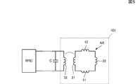
- FIG. 5 is a circuit diagram of a wireless communication circuit including the antenna device 101.
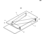
- FIG. 6 is a perspective view of the antenna device 102 according to the second embodiment.
- FIG. 7A is a perspective view of a main part of a communication terminal apparatus including the antenna device 103 according to the third embodiment, and
- FIG. 7B is a perspective view of a main part of the communication terminal apparatus including an antenna apparatus of a comparative example. It is.
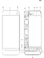
- FIG. 8 is a plan view showing the structure inside the housing of the communication terminal apparatus according to the fourth embodiment.
- FIG. 9 is a cross-sectional view of the communication terminal device at a position passing through the first connection conductor 21 and the second connection conductor 22.
- FIG. 10 is a cross-sectional view of another communication terminal device at a position passing through the first connection conductor 21 and the second connection conductor 22.
- FIG. 1A is a perspective view of an antenna device 101 according to the first embodiment
- FIG. 1B is a perspective view of an antenna coil 30 provided in the antenna device 101
- FIG. 2 is a cross-sectional view taken along the line AA ′ in FIG.
- the antenna device 101 is an antenna that is used in an HF band such as 13.56 MHz, for example, and is electromagnetically coupled (mainly magnetically coupled) with a communication partner antenna in a proximity type or a proximity type.
- the antenna device 101 includes a first conductor surface 11 and a second conductor surface 12 that face each other.
- the first conductor surface 11 and the second conductor surface 12 are connected by a first connection conductor 21 and a second connection conductor 22.
- An antenna coil 30 is disposed between the first conductor surface 11 and the second conductor surface 12 and close to the first connection conductor 21.
- the antenna coil 30 is composed of a magnetic core 31 and a coil conductor 32, and the coil conductor 32 has a pattern that winds around the magnetic core 31. Is formed.
- a chip-type antenna in which a rectangular helical coil conductor is built in a laminated body by forming coil conductor patterns on a plurality of resin sheets in which magnetic ferrite fillers are dispersed, laminating them, and thermocompression bonding them. is there.
- the antenna coil 30 may be a chip antenna having a magnetic ferrite ceramic body.
- the antenna coil 30 is disposed in the vicinity of the first connection conductor 21 so that a portion of the coil conductor 32 included in the antenna coil 30 that is close to the first connection conductor 21 is in parallel with the first connection conductor 21. Yes.
- the first conductor surface 11 is, for example, a ground electrode pattern of a circuit board.
- the second conductor surface 12 is, for example, a metal part of the housing.
- the first connection conductor 21 and the second connection conductor 22 are spring pin terminals, respectively, and electrically connect the first conductor surface 11 and the second conductor surface 12 directly. These pin terminals are originally ground connection pins that make the metal part of the housing and the ground electrode of the circuit board have the same potential. However, in this embodiment, as will be described later, the first conductor surface 11 and the second conductor terminal are used. It also serves as a current path for passing a current through the conductor surface 12.
- FIG. 3A is a front view showing paths of currents flowing through the respective parts of the antenna device 101
- FIG. 3B is a front view showing paths of currents flowing through the respective parts of the antenna device of the comparative example.
- the two connection conductors 21 and 22 and the two conductor surfaces 11 and 12 form a closed loop.
- the antenna coil 30 is disposed at a position that does not overlap the opening surface. And it arrange
- the antenna coil 30 is disposed at a position overlapping the closed loop opening surface. Then, an induction current flows through the first connection conductor 21 by electromagnetic induction of the antenna coil 30.
- the first connection conductor 21 and the coil conductor 32 adjacent thereto are The parts are inductively coupled. That is, an induced current flows through the first connecting conductor 21 in the direction opposite to the direction of the current flowing through the coil conductor 32 of the antenna coil 30.
- This current circulates in a closed loop along the path of the second conductor surface 12 ⁇ the second connection conductor 22 ⁇ the first conductor surface 11 ⁇ the first connection conductor 21.
- the magnetic field generated by the current flowing through the closed loop and the magnetic field generated by the current flowing through the antenna coil 30 have opposite directions (polarities). Therefore, the magnetic field is canceled out, and this antenna device does not actually function as an antenna.
- an induced current is applied to the first connection conductor 21 in the direction opposite to the direction of the current flowing through the coil conductor 32 of the antenna coil 30. Flowing. This current circulates in a closed loop along the path of the first conductor surface 11 ⁇ the second connection conductor 22 ⁇ the second conductor surface 12 ⁇ the first connection conductor 21.
- the direction (polarity) of the magnetic field generated by the current flowing through the closed loop and the magnetic field generated by the current flowing through the antenna coil 30 are the same. Therefore, the first conductor surface 11, the second conductor surface 12, the first connection conductor 21 and the second connection conductor 22 constituting the closed loop act as a booster antenna, and the antenna coil 30 functions as the booster antenna and the feeding coil. And acts as an antenna device.
- FIG. 4 (A) is a cross-sectional view taken along the line BB ′ in FIG. 1 (A), and is a schematic view of the radiated magnetic flux.
- FIG. 4B is a perspective view showing a path of a current flowing through the antenna device 101.
- FIGS. 4A and 4B when current flows through the first conductor surface 11 and the second conductor surface 12, the first conductor surface 11, the second conductor surface 12, the first connection conductor 21 and the second conductor A magnetic field through which the magnetic flux ⁇ passes through the closed loop by the connection conductor 22 (see FIG. 2) is generated.
- This magnetic flux ⁇ is linked to the communication partner antenna coil for communication.
- the antenna device 101 is used as an antenna for NFC communication using 13.56 MHz, for example.
- FIG. 5 is a circuit diagram of a wireless communication circuit including the antenna device 101.
- a closed loop AR formed by the first conductor surface 11, the second conductor surface 12, the first connection conductor 21, and the second connection conductor 22 is represented by a closed loop circuit of an inductor.
- the coil conductor 32 of the antenna coil 30 is inductively coupled to the first connection conductor 21.
- a high frequency IC (RFIC) is connected to the coil conductor 32.
- RFIC high frequency IC
- a resonance capacitor C is connected in parallel to the coil conductor 32, and the capacitance of the capacitor C and the coil conductor so that the resonance frequency of the capacitor C and the coil conductor 32 is at or near the carrier frequency of the communication signal. 32 inductances are defined.
- FIG. 6 is a perspective view of the antenna device 102 according to the second embodiment.
- the antenna device 102 includes a first conductor surface 11 and a second conductor surface 12 that face each other.
- the first conductor surface 11 and the second conductor surface 12 are connected by a first connection conductor 21, a second connection conductor 22, a third connection conductor 23, and a fourth connection conductor 24, respectively.
- An antenna coil 30 is disposed between the first conductor surface 11 and the second conductor surface 12 and close to the first connection conductor 21. In the example shown in FIG.
- the antenna coil 30 is disposed at a position that does not overlap any of the closed loop opening surfaces. Therefore, the first conductor surface 11, the second conductor surface 12, and the connection conductors 21, 22, 23, and 24 function as a booster antenna so that the magnetic flux passes through each of these closed loops.
- the ground electrode of the substrate and the metal part of the housing are used so that the current flows not only in the short side direction of the ground electrode of the substrate and the metal part of the housing but also in the long side direction. be able to.
- FIG. 7A is a perspective view of a main part of a communication terminal apparatus including the antenna device 103 according to the third embodiment
- FIG. 7B is a perspective view of a main part of the communication terminal apparatus including an antenna apparatus of a comparative example. It is.
- a UHF band antenna 81 is disposed on a circuit board on which a ground electrode as the first conductor surface 11 is formed. 7A and 7B, the antenna 81 is an inverted F-type antenna, but is schematically represented by a conductor line in the drawing. This UHF band antenna is used for cellular phone calls and data communications.
- the first connection conductor 21 is formed (placed) inside the edges of the first conductor surface 11 and the second conductor surface 12 in the antenna device 103 of the present embodiment shown in FIG.
- the other connection conductors 22 and 25 are formed (arranged) on the edges of the first conductor surface 11 and the second conductor surface 12.
- the connection conductor 25 conducts between the land 25L and the second conductor surface 12.
- a chip capacitor 5 is mounted between the land 25 ⁇ / b> L and the first conductor surface 11. That is, in the connection conductor 25 portion, the first conductor surface 11 and the second conductor surface 12 are connected via the chip capacitor 5.
- the chip capacitor 5 is an element that has high impedance in the frequency band (HF band) of the carrier frequency of the communication signal, but has low impedance in the frequency above the UHF band. That is, the chip capacitor 5 is difficult to conduct in the HF band, but is easy to conduct in the UHF band.
- the first connection conductor 21 and the second connection conductor 22 are formed (arranged) on the edges of the first conductor surface 11 and the second conductor surface 12.
- the broken-line arrows in the figure represent the current path. Basically, a substrate current flows through the first conductor surface 11 (the ground electrode of the circuit board), and a housing current flows through the second conductor surface 12 (the metal part of the housing). The substrate current and the housing current flow through the connection conductors 21 and 22 and the like.
- the substrate current from the UHF band antenna 81 affects the ferrite of the antenna coil 30. Effect. As a result, loss is caused by the ferrite, and the characteristics of the UHF band antenna 81 deteriorate.
- the antenna coil 30 is arranged on the inner side of the edge of the first conductor surface 11, so that the substrate current by the antenna 81 in the UHF band is Does not pass through the connection conductor 21 but passes through the chip capacitor 5 and the connection conductor 25 (the chip capacitor 5 is easy to conduct in the UHF band). That is, the substrate current generated by the UHF band antenna 81 hardly affects the ferrite of the antenna coil 30. Therefore, the characteristics of the UHF band antenna 81 can be maintained. Since the chip capacitor 5 has high impedance in the HF band, the loop formed by the two conductor surfaces 11 and 12 and the two connection conductors 21 and 25 is not a closed loop but an open loop.
- the member constituting the closed loop functions as a booster antenna of the HF band antenna.
- FIG. 8 is a plan view showing the structure inside the housing of the communication terminal apparatus according to the fourth embodiment.
- circuit boards 61 and 62 In the upper casing 91, circuit boards 61 and 62, a battery pack 90, a camera module 76, and the like are housed.
- an RFIC 60 including a communication circuit, a resonance capacitor C, an antenna coil 30, and the like are mounted.
- the circuit board 61 is also provided with a main UHF band antenna 82 and the like.
- the circuit board 62 is provided with a sub UHF band antenna 83 and the like.
- the circuit on the circuit board 61 and the circuit on the circuit board 62 are connected via a cable.
- the UHF band antennas 82 and 83 are provided by mounting a chip antenna or forming a line pattern.
- the circuit board 61 has a ground electrode formed in almost the entire region, and the formed ground electrode functions as a first conductor surface.
- the lower casing 92 is made of resin, and the second conductor surface 12 is formed on the inner surface thereof by a metal film.
- This metal film may be one in which an aluminum foil or a copper foil is attached to the inside of the casing 92, or may be drawn on the inside of the casing 92 by the LDS technique or the like.
- the metal film preferably occupies more than half of the main surface of the circuit board 61 for the purpose of serving as a shield for various components mounted on the circuit board 61 and the like. In the present embodiment, almost all areas except the area occupied by the main antenna 82 and the sub antenna 83 are shielded by the metal film.
- An opening 12 ⁇ / b> A is formed in the lower housing 92. In this portion, the lens of the camera module 76 is disposed so as to be optically exposed.
- the first connection conductor 21 and the second connection conductor 22 are mounted on the circuit board 61.
- FIG. 9 is a cross-sectional view at a position passing through the first connection conductor 21 and the second connection conductor 22.
- a current flows through the first conductor surface (ground electrode) 11 and the second conductor surface (metal part of the housing) 12.
- a current flows in a closed loop formed by the two conductor surfaces 11 and 12 and the two connection conductors 21 and 22. In this way, the two conductor surfaces 11 and 12 act as a radiating element, and the closed loop opening surface acts as a radiating element.
- the antenna coil 30 and the RFIC 60 may be integrated and modularized. With this configuration, it is not necessary to perform electrical continuity between the RFIC and the power supply coil by wiring on a substrate such as a circuit substrate, and the degree of freedom in mounting space is increased.
- the antenna coil 30 is mounted on the first conductor surface (ground electrode) formed on the circuit board 61, but the antenna coil 30 is the first conductor. It is preferable to mount the circuit board 61 on which no surface (ground electrode) is formed.
- FIG. 10 is a cross-sectional view at a position passing through the first connection conductor 21 and the second connection conductor 22 in a communication terminal device different from that in FIG. 9, and a circuit in which the first conductor surface (ground electrode) is not formed. Except that the antenna coil 30 is mounted on the substrate 61, it is almost the same as the communication terminal device shown in FIG. With this configuration, predetermined antenna characteristics can be obtained without the first conductor surface (ground electrode) interfering with the magnetic field generated from the antenna coil 30.
- one of the first conductor surface and the second conductor surface according to the present invention is not limited to the ground electrode formed on the circuit board.
- one side is not restricted to the metal part of a housing
- a shield case, a shield plate, a battery pack, an LCD panel, or the like may be used as the first conductor surface or the second conductor surface.
- the second conductor surface may be a metal part of a housing on the side where the circuit board is accommodated. Furthermore, the metal part of the housing may be a molded body of a metal plate.
Landscapes
- Engineering & Computer Science (AREA)
- Computer Networks & Wireless Communication (AREA)
- Support Of Aerials (AREA)
- Details Of Aerials (AREA)
Abstract
Description
前記複数の接続導体のうち2つの接続導体と前記2つの導体面とで開口を有する閉ループが形成されていて、前記アンテナコイルは、前記閉ループの開口面を平面視したときに、前記開口面に重ならない位置で、且つ前記アンテナコイルの電磁誘導により前記接続導体に誘導電流が流れる位置に配置されていることを特徴とする。
アンテナ装置と、このアンテナ装置に接続された給電回路とを備え、
前記アンテナ装置は、
空間を介して対向する位置に配置されている2つの導体面と、
前記2つの導体面を少なくとも2箇所でそれぞれ接続する複数の接続導体と、
前記複数の接続導体のうち少なくとも1つの接続導体に対して近接配置されたアンテナコイルと、を備え、
前記複数の接続導体のうち2つの接続導体と前記2つの導体面とで開口を有する閉ループが形成されていて、
前記アンテナコイルは、前記閉ループの開口面を平面視したときに、前記開口面に重ならない位置で、且つ前記アンテナコイルの電磁誘導により前記接続導体に誘導電流が流れる位置に配置されていることを特徴とする。
図1(A)は第1の実施形態に係るアンテナ装置101の斜視図、図1(B)はアンテナ装置101に設けられているアンテナコイル30の斜視図である。図2は、図1(A)におけるA-A′断面図である。このアンテナ装置101は、例えば13.56MHz等のHF帯で用い、通信相手のアンテナと近接型または近傍型で電磁界結合(主に磁界結合)するアンテナである。
図6は第2の実施形態に係るアンテナ装置102の斜視図である。このアンテナ装置102は、互いに対向する第1導体面11および第2導体面12を備えている。第1導体面11と第2導体面12とは、第1接続導体21、第2接続導体22、第3接続導体23および第4接続導体24でそれぞれ接続されている。第1導体面11と第2導体面12との間で、且つ第1接続導体21に近接してアンテナコイル30が配置されている。図6に示した例では、接続導体21,22と導体面11,12とによる閉ループ、接続導体21,23と導体面11,12とによる閉ループ、接続導体21,24と導体面11,12とによる閉ループがそれぞれ構成される。アンテナコイル30は、このいずれの閉ループの開口面にも重ならない位置に配置されている。そのため、これらの閉ループをそれぞれ磁束が通るように、第1導体面11、第2導体面12、および接続導体21,22,23,24は、ブースターアンテナとして作用する。
図7(A)は第3の実施形態に係るアンテナ装置103を備える通信端末装置の主要部の斜視図、図7(B)は比較例のアンテナ装置を備える通信端末装置の主要部の斜視図である。これらの通信端末装置は、第1導体面11であるグランド電極が形成された回路基板にUHF帯のアンテナ81が配置されたものである。図7(A)(B)においては、アンテナ81は逆F型アンテナであるが、図においては導体線によって模式的に表している。このUHF帯のアンテナは携帯電話の通話およびデータ通信のために使用される。
図8は第4の実施形態に係る通信端末装置の筐体内部の構造を示す平面図である。上部筐体91の内部には回路基板61,62、バッテリーパック90、カメラモジュール76等が収められている。回路基板61には通信回路を備えたRFIC60、共振用キャパシタC、アンテナコイル30等が実装されている。この回路基板61にはメインのUHF帯アンテナ82等も設けられている。また、回路基板62にはサブのUHF帯アンテナ83等が設けられている。回路基板61上の回路と回路基板62上の回路とはケーブルを介して接続されている。UHF帯アンテナ82,83はチップアンテナの搭載や線路パターンの形成等によって設けられている。
5…チップキャパシタ
11…第1導体面
12…第2導体面
12A…開口
21~25…接続導体
21…第1接続導体
22…第2接続導体
25L…ランド
30…アンテナコイル
31…磁性体コア
32…コイル導体
60…RFIC
61,62…回路基板
76…カメラモジュール
81,82,83…UHF帯アンテナ
90…バッテリーパック
91…上部筐体
92…下部筐体
101,102,103…アンテナ装置
Claims (7)
- 空間を介して対向する位置に配置されている2つの導体面と、
前記2つの導体面を少なくとも2箇所でそれぞれ接続する複数の接続導体と、
前記複数の接続導体のうち少なくとも1つの接続導体に対して近接配置されたアンテナコイルと、を備え、
前記複数の接続導体のうち2つの接続導体と前記2つの導体面とで、開口を有する閉ループが形成されていて、
前記アンテナコイルは、前記閉ループの開口面を平面視したときに、前記開口面に重ならない位置で、且つ前記アンテナコイルの電磁誘導により前記接続導体に誘導電流が流れる位置に配置されていることを特徴とするアンテナ装置。 - 前記接続導体は3つ以上あって、
前記アンテナコイルは、隣り合う2つの接続導体と2つの導体板とで形成される複数のループの開口面からそれぞれ平面視したとき、いずれの開口面にも重ならない位置に配置されている、請求項1に記載のアンテナ装置。 - 前記導体面は、電子機器の筐体の導体部を含む、請求項1または2に記載のアンテナ装置。
- 前記導体面は、回路基板に形成されたグランド電極を含む、請求項1~3のいずれかに記載のアンテナ装置。
- 前記導体面は、回路基板に形成されたグランド電極と電子機器の筐体の導体部とを含み、前記接続導体は、前記グランド電極と前記筐体の導体部とを接続するグランド接続ピンである、請求項1または2に記載のアンテナ装置。
- 前記複数の接続導体のうち前記閉ループの一部でない接続導体と前記導体面とはキャパシタを介して接続され、
通信信号のキャリア周波数はHF帯の周波数であり、前記キャパシタはUHF帯以上の周波数でHF帯の周波数よりもロー・インピーダンスとなる素子である、請求項5に記載のアンテナ装置。 - アンテナ装置と、このアンテナ装置に接続された給電回路とを備えた通信端末装置において、
前記アンテナ装置は、
空間を介して対向する位置に配置されている2つの導体面と、
前記2つの導体面を少なくとも2箇所でそれぞれ接続する複数の接続導体と、
前記複数の接続導体のうち少なくとも1つの接続導体に対して近接配置されたアンテナコイルと、を備え、
前記複数の接続導体のうち2つの接続導体と前記2つの導体面とで開口を有する閉ループが形成されていて、
前記アンテナコイルは、前記閉ループの開口面を平面視したときに、前記開口面に重ならない位置で、且つ前記アンテナコイルの電磁誘導により前記接続導体に誘導電流が流れる位置に配置されていることを特徴とする、通信端末装置。
Priority Applications (4)
| Application Number | Priority Date | Filing Date | Title |
|---|---|---|---|
| JP2014555642A JP5692483B1 (ja) | 2013-06-14 | 2014-06-03 | アンテナ装置および通信端末装置 |
| EP14810308.8A EP2897221B1 (en) | 2013-06-14 | 2014-06-03 | Antenna device and communication-terminal device |
| CN201480002030.4A CN104508909B (zh) | 2013-06-14 | 2014-06-03 | 天线装置及通信终端装置 |
| US14/594,268 US9634380B2 (en) | 2013-06-14 | 2015-01-12 | Antenna device and communication terminal device |
Applications Claiming Priority (2)
| Application Number | Priority Date | Filing Date | Title |
|---|---|---|---|
| JP2013-125185 | 2013-06-14 | ||
| JP2013125185 | 2013-06-14 |
Related Child Applications (1)
| Application Number | Title | Priority Date | Filing Date |
|---|---|---|---|
| US14/594,268 Continuation US9634380B2 (en) | 2013-06-14 | 2015-01-12 | Antenna device and communication terminal device |
Publications (1)
| Publication Number | Publication Date |
|---|---|
| WO2014199861A1 true WO2014199861A1 (ja) | 2014-12-18 |
Family
ID=52022159
Family Applications (1)
| Application Number | Title | Priority Date | Filing Date |
|---|---|---|---|
| PCT/JP2014/064665 Ceased WO2014199861A1 (ja) | 2013-06-14 | 2014-06-03 | アンテナ装置および通信端末装置 |
Country Status (5)
| Country | Link |
|---|---|
| US (1) | US9634380B2 (ja) |
| EP (1) | EP2897221B1 (ja) |
| JP (2) | JP5692483B1 (ja) |
| CN (1) | CN104508909B (ja) |
| WO (1) | WO2014199861A1 (ja) |
Cited By (4)
| Publication number | Priority date | Publication date | Assignee | Title |
|---|---|---|---|---|
| EP3041084A1 (en) * | 2015-01-05 | 2016-07-06 | LG Electronics Inc. | Antenna module and mobile terminal having the same |
| JP2017005610A (ja) * | 2015-06-15 | 2017-01-05 | Tdk株式会社 | アンテナ装置及びこれに用いるコイル部品 |
| JP6601597B1 (ja) * | 2018-05-11 | 2019-11-06 | 株式会社村田製作所 | 無線通信デバイス、およびそれを備えた物品 |
| WO2019215963A1 (ja) * | 2018-05-11 | 2019-11-14 | 株式会社村田製作所 | 無線通信デバイス、およびそれを備えた物品 |
Families Citing this family (5)
| Publication number | Priority date | Publication date | Assignee | Title |
|---|---|---|---|---|
| JP6627252B2 (ja) * | 2015-04-28 | 2020-01-08 | Tdk株式会社 | アンテナ装置 |
| WO2017006921A1 (ja) * | 2015-07-06 | 2017-01-12 | 株式会社村田製作所 | アンテナ装置および電子機器 |
| KR102280037B1 (ko) * | 2015-07-29 | 2021-07-21 | 삼성전자주식회사 | 디스플레이에 구비된 내장 안테나용 급전장치 |
| CN208674354U (zh) * | 2015-12-14 | 2019-03-29 | 株式会社村田制作所 | 天线装置及电子设备 |
| KR20170103315A (ko) * | 2016-03-03 | 2017-09-13 | 엘지전자 주식회사 | 이동 단말기 |
Citations (5)
| Publication number | Priority date | Publication date | Assignee | Title |
|---|---|---|---|---|
| JPH11112226A (ja) * | 1997-09-30 | 1999-04-23 | Kokusai Electric Co Ltd | 偏波面切替えアンテナ |
| JP4993045B2 (ja) | 2009-04-21 | 2012-08-08 | 株式会社村田製作所 | アンテナ装置及び電子機器 |
| WO2012173080A1 (ja) * | 2011-06-13 | 2012-12-20 | 株式会社村田製作所 | アンテナ装置および通信端末装置 |
| JP2013055637A (ja) * | 2011-08-10 | 2013-03-21 | Murata Mfg Co Ltd | アンテナ装置および通信端末装置 |
| JP5532191B1 (ja) * | 2012-06-28 | 2014-06-25 | 株式会社村田製作所 | アンテナ装置および通信端末装置 |
Family Cites Families (12)
| Publication number | Priority date | Publication date | Assignee | Title |
|---|---|---|---|---|
| JP2652988B2 (ja) * | 1989-11-30 | 1997-09-10 | 日本電気株式会社 | 選択呼出受信機のアンテナ |
| US5268699A (en) * | 1992-09-24 | 1993-12-07 | Motorola, Inc. | Data communication receiver utilizing a loop antenna having a hinged connection |
| JPH09182133A (ja) * | 1995-12-21 | 1997-07-11 | Kokusai Electric Co Ltd | カード型無線呼出受信機 |
| FI113217B (fi) * | 2000-10-18 | 2004-03-15 | Filtronic Lk Oy | Kaksitoiminen antenni ja radiolaite |
| CN1244180C (zh) * | 2001-01-30 | 2006-03-01 | 松下电器产业株式会社 | 天线 |
| WO2005053095A1 (ja) * | 2003-11-28 | 2005-06-09 | Fujitsu Limited | 非接触リーダおよび/またはライタを具える情報処理装置、および磁気的結合用のコイル・アンテナ |
| WO2008133018A1 (ja) * | 2007-04-13 | 2008-11-06 | Murata Manufacturing Co., Ltd. | 磁界結合型アンテナ、磁界結合型アンテナモジュールおよび磁界結合型アンテナ装置、ならびにこれらの製造方法 |
| DE102007062051A1 (de) * | 2007-12-21 | 2009-06-25 | Siemens Home And Office Communication Devices Gmbh & Co. Kg | Antennenvorrichtung für funkbasierte elektronische Geräte |
| JP2010028351A (ja) * | 2008-07-17 | 2010-02-04 | Fujikura Ltd | ブースターアンテナ及び非接触情報媒体 |
| US20100048265A1 (en) * | 2008-08-21 | 2010-02-25 | Chi-Ming Chiang | Antenna mounting arrangement for cell phone with a metal casing |
| TW201134000A (en) * | 2010-03-16 | 2011-10-01 | Chi Mei Comm Systems Inc | Wireless communication device |
| US8577289B2 (en) * | 2011-02-17 | 2013-11-05 | Apple Inc. | Antenna with integrated proximity sensor for proximity-based radio-frequency power control |
-
2014
- 2014-06-03 EP EP14810308.8A patent/EP2897221B1/en not_active Not-in-force
- 2014-06-03 JP JP2014555642A patent/JP5692483B1/ja not_active Expired - Fee Related
- 2014-06-03 CN CN201480002030.4A patent/CN104508909B/zh active Active
- 2014-06-03 WO PCT/JP2014/064665 patent/WO2014199861A1/ja not_active Ceased
-
2015
- 2015-01-12 US US14/594,268 patent/US9634380B2/en active Active
- 2015-02-05 JP JP2015021107A patent/JP5928621B2/ja not_active Expired - Fee Related
Patent Citations (5)
| Publication number | Priority date | Publication date | Assignee | Title |
|---|---|---|---|---|
| JPH11112226A (ja) * | 1997-09-30 | 1999-04-23 | Kokusai Electric Co Ltd | 偏波面切替えアンテナ |
| JP4993045B2 (ja) | 2009-04-21 | 2012-08-08 | 株式会社村田製作所 | アンテナ装置及び電子機器 |
| WO2012173080A1 (ja) * | 2011-06-13 | 2012-12-20 | 株式会社村田製作所 | アンテナ装置および通信端末装置 |
| JP2013055637A (ja) * | 2011-08-10 | 2013-03-21 | Murata Mfg Co Ltd | アンテナ装置および通信端末装置 |
| JP5532191B1 (ja) * | 2012-06-28 | 2014-06-25 | 株式会社村田製作所 | アンテナ装置および通信端末装置 |
Cited By (5)
| Publication number | Priority date | Publication date | Assignee | Title |
|---|---|---|---|---|
| EP3041084A1 (en) * | 2015-01-05 | 2016-07-06 | LG Electronics Inc. | Antenna module and mobile terminal having the same |
| US9755298B2 (en) | 2015-01-05 | 2017-09-05 | Lg Electronics Inc. | Antenna module and mobile terminal having the same |
| JP2017005610A (ja) * | 2015-06-15 | 2017-01-05 | Tdk株式会社 | アンテナ装置及びこれに用いるコイル部品 |
| JP6601597B1 (ja) * | 2018-05-11 | 2019-11-06 | 株式会社村田製作所 | 無線通信デバイス、およびそれを備えた物品 |
| WO2019215963A1 (ja) * | 2018-05-11 | 2019-11-14 | 株式会社村田製作所 | 無線通信デバイス、およびそれを備えた物品 |
Also Published As
| Publication number | Publication date |
|---|---|
| JPWO2014199861A1 (ja) | 2017-02-23 |
| US20150123858A1 (en) | 2015-05-07 |
| EP2897221A4 (en) | 2015-11-18 |
| CN104508909B (zh) | 2017-04-12 |
| JP5692483B1 (ja) | 2015-04-01 |
| EP2897221A1 (en) | 2015-07-22 |
| JP5928621B2 (ja) | 2016-06-01 |
| JP2015092775A (ja) | 2015-05-14 |
| US9634380B2 (en) | 2017-04-25 |
| CN104508909A (zh) | 2015-04-08 |
| EP2897221B1 (en) | 2017-08-16 |
Similar Documents
| Publication | Publication Date | Title |
|---|---|---|
| JP5692483B1 (ja) | アンテナ装置および通信端末装置 | |
| JP5772868B2 (ja) | アンテナ装置および無線通信装置 | |
| US10116042B2 (en) | Antenna device and communication terminal device | |
| JP6256600B2 (ja) | アンテナ装置および電子機器 | |
| JP5673906B1 (ja) | 通信端末 | |
| CN103620868B (zh) | 天线装置及通信终端装置 | |
| JP5776868B1 (ja) | アンテナ装置および電子機器 | |
| JP5686232B1 (ja) | アンテナ装置および通信端末装置 | |
| WO2016121501A1 (ja) | アンテナ装置、カード型情報媒体および通信端末装置 |
Legal Events
| Date | Code | Title | Description |
|---|---|---|---|
| ENP | Entry into the national phase |
Ref document number: 2014555642 Country of ref document: JP Kind code of ref document: A |
|
| REEP | Request for entry into the european phase |
Ref document number: 2014810308 Country of ref document: EP |
|
| WWE | Wipo information: entry into national phase |
Ref document number: 2014810308 Country of ref document: EP |
|
| 121 | Ep: the epo has been informed by wipo that ep was designated in this application |
Ref document number: 14810308 Country of ref document: EP Kind code of ref document: A1 |
|
| NENP | Non-entry into the national phase |
Ref country code: DE |