WO2014203724A1 - Dispositif de contact électrique, unité de lentille, et dispositif d'imagerie - Google Patents
Dispositif de contact électrique, unité de lentille, et dispositif d'imagerie Download PDFInfo
- Publication number
- WO2014203724A1 WO2014203724A1 PCT/JP2014/064704 JP2014064704W WO2014203724A1 WO 2014203724 A1 WO2014203724 A1 WO 2014203724A1 JP 2014064704 W JP2014064704 W JP 2014064704W WO 2014203724 A1 WO2014203724 A1 WO 2014203724A1
- Authority
- WO
- WIPO (PCT)
- Prior art keywords
- base
- contact
- end side
- electrical contact
- substrate
- Prior art date
- Legal status (The legal status is an assumption and is not a legal conclusion. Google has not performed a legal analysis and makes no representation as to the accuracy of the status listed.)
- Ceased
Links
Images


Classifications
-
- G—PHYSICS
- G03—PHOTOGRAPHY; CINEMATOGRAPHY; ANALOGOUS TECHNIQUES USING WAVES OTHER THAN OPTICAL WAVES; ELECTROGRAPHY; HOLOGRAPHY
- G03B—APPARATUS OR ARRANGEMENTS FOR TAKING PHOTOGRAPHS OR FOR PROJECTING OR VIEWING THEM; APPARATUS OR ARRANGEMENTS EMPLOYING ANALOGOUS TECHNIQUES USING WAVES OTHER THAN OPTICAL WAVES; ACCESSORIES THEREFOR
- G03B17/00—Details of cameras or camera bodies; Accessories therefor
- G03B17/02—Bodies
- G03B17/12—Bodies with means for supporting objectives, supplementary lenses, filters, masks, or turrets
- G03B17/14—Bodies with means for supporting objectives, supplementary lenses, filters, masks, or turrets interchangeably
-
- H—ELECTRICITY
- H01—ELECTRIC ELEMENTS
- H01R—ELECTRICALLY-CONDUCTIVE CONNECTIONS; STRUCTURAL ASSOCIATIONS OF A PLURALITY OF MUTUALLY-INSULATED ELECTRICAL CONNECTING ELEMENTS; COUPLING DEVICES; CURRENT COLLECTORS
- H01R12/00—Structural associations of a plurality of mutually-insulated electrical connecting elements, specially adapted for printed circuits, e.g. printed circuit boards [PCB], flat or ribbon cables, or like generally planar structures, e.g. terminal strips, terminal blocks; Coupling devices specially adapted for printed circuits, flat or ribbon cables, or like generally planar structures; Terminals specially adapted for contact with, or insertion into, printed circuits, flat or ribbon cables, or like generally planar structures
- H01R12/50—Fixed connections
- H01R12/59—Fixed connections for flexible printed circuits, flat or ribbon cables or like structures
-
- H—ELECTRICITY
- H01—ELECTRIC ELEMENTS
- H01R—ELECTRICALLY-CONDUCTIVE CONNECTIONS; STRUCTURAL ASSOCIATIONS OF A PLURALITY OF MUTUALLY-INSULATED ELECTRICAL CONNECTING ELEMENTS; COUPLING DEVICES; CURRENT COLLECTORS
- H01R12/00—Structural associations of a plurality of mutually-insulated electrical connecting elements, specially adapted for printed circuits, e.g. printed circuit boards [PCB], flat or ribbon cables, or like generally planar structures, e.g. terminal strips, terminal blocks; Coupling devices specially adapted for printed circuits, flat or ribbon cables, or like generally planar structures; Terminals specially adapted for contact with, or insertion into, printed circuits, flat or ribbon cables, or like generally planar structures
- H01R12/70—Coupling devices
- H01R12/71—Coupling devices for rigid printing circuits or like structures
- H01R12/712—Coupling devices for rigid printing circuits or like structures co-operating with the surface of the printed circuit or with a coupling device exclusively provided on the surface of the printed circuit
- H01R12/714—Coupling devices for rigid printing circuits or like structures co-operating with the surface of the printed circuit or with a coupling device exclusively provided on the surface of the printed circuit with contacts abutting directly the printed circuit; Button contacts therefore provided on the printed circuit
-
- H—ELECTRICITY
- H01—ELECTRIC ELEMENTS
- H01R—ELECTRICALLY-CONDUCTIVE CONNECTIONS; STRUCTURAL ASSOCIATIONS OF A PLURALITY OF MUTUALLY-INSULATED ELECTRICAL CONNECTING ELEMENTS; COUPLING DEVICES; CURRENT COLLECTORS
- H01R13/00—Details of coupling devices of the kinds covered by groups H01R12/70 or H01R24/00 - H01R33/00
- H01R13/02—Contact members
- H01R13/22—Contacts for co-operating by abutting
- H01R13/24—Contacts for co-operating by abutting resilient; resiliently-mounted
-
- H—ELECTRICITY
- H04—ELECTRIC COMMUNICATION TECHNIQUE
- H04N—PICTORIAL COMMUNICATION, e.g. TELEVISION
- H04N23/00—Cameras or camera modules comprising electronic image sensors; Control thereof
- H04N23/50—Constructional details
- H04N23/55—Optical parts specially adapted for electronic image sensors; Mounting thereof
-
- H—ELECTRICITY
- H04—ELECTRIC COMMUNICATION TECHNIQUE
- H04N—PICTORIAL COMMUNICATION, e.g. TELEVISION
- H04N23/00—Cameras or camera modules comprising electronic image sensors; Control thereof
- H04N23/60—Control of cameras or camera modules
- H04N23/67—Focus control based on electronic image sensor signals
-
- H—ELECTRICITY
- H04—ELECTRIC COMMUNICATION TECHNIQUE
- H04N—PICTORIAL COMMUNICATION, e.g. TELEVISION
- H04N23/00—Cameras or camera modules comprising electronic image sensors; Control thereof
- H04N23/70—Circuitry for compensating brightness variation in the scene
- H04N23/73—Circuitry for compensating brightness variation in the scene by influencing the exposure time
-
- G—PHYSICS
- G03—PHOTOGRAPHY; CINEMATOGRAPHY; ANALOGOUS TECHNIQUES USING WAVES OTHER THAN OPTICAL WAVES; ELECTROGRAPHY; HOLOGRAPHY
- G03B—APPARATUS OR ARRANGEMENTS FOR TAKING PHOTOGRAPHS OR FOR PROJECTING OR VIEWING THEM; APPARATUS OR ARRANGEMENTS EMPLOYING ANALOGOUS TECHNIQUES USING WAVES OTHER THAN OPTICAL WAVES; ACCESSORIES THEREFOR
- G03B2206/00—Systems for exchange of information between different pieces of apparatus, e.g. for exchanging trimming information, for photo finishing
-
- G—PHYSICS
- G03—PHOTOGRAPHY; CINEMATOGRAPHY; ANALOGOUS TECHNIQUES USING WAVES OTHER THAN OPTICAL WAVES; ELECTROGRAPHY; HOLOGRAPHY
- G03B—APPARATUS OR ARRANGEMENTS FOR TAKING PHOTOGRAPHS OR FOR PROJECTING OR VIEWING THEM; APPARATUS OR ARRANGEMENTS EMPLOYING ANALOGOUS TECHNIQUES USING WAVES OTHER THAN OPTICAL WAVES; ACCESSORIES THEREFOR
- G03B2217/00—Details of cameras or camera bodies; Accessories therefor
- G03B2217/002—Details of arrangement of components in or on camera body
Definitions
- the present invention relates to an electrical contact device for electrically connecting a camera unit and a replaceable lens unit, a lens unit having the electrical contact device, and an imaging device.
- the camera body is provided with an image sensor and a control circuit board for controlling each part such as the image sensor, and a lens mount on which a lens unit is mounted is provided on the front surface.
- the lens unit is a unit in which a lens, a diaphragm, an optical filter, and the like are integrated.
- a control circuit board is provided not only in the camera body but also in the lens unit.
- the control circuit board of the lens unit is connected via an electrical contact device provided on the lens mount, sends and receives control signals for automatic exposure control and automatic focus adjustment to the camera body, and the lens position and aperture opening amount.
- An electrical contact device that connects a lens unit and a camera body includes, for example, a substrate on which a conductive pattern is formed, a contact member that is fixed to the substrate by being caulked against a hole formed in the substrate, and a contact member Comprising a base that can be displaced between a protruding position and a retracted position, a biasing member that biases the substrate in a direction to press the substrate against the contact member, and a support member that supports the biasing member.
- Patent Document 1 Known (Patent Document 1).
- the electrical contact apparatus of patent document 1 has fixed the contact member to the board
- the contact member is fixed to the substrate by caulking and the urging member is supported only by the supporting member, when the caulking is loosened, the urging is caused by a gap between the urging member and the inner wall of the base.
- the member wobbles, for example, the urging member is bent in the middle, and instability is further promoted.
- An object of the present invention is to provide an electrical contact device having a short distance from the contact member to the side surface of the lens unit, and a camera body, a lens unit, and an imaging device having the electrical contact device.
- the electrical contact device of the present invention is an electrical contact device for electrically connecting the camera body and the lens unit, and includes a substrate, a contact member, a base, a biasing member, a support member, and a guide portion.
- a conductive pattern is formed on the substrate, and the contact member is in direct contact with the substrate and electrically connected to the conductive pattern.
- the base has a first hole portion that holds a position between a protruding position where one end of the contact member protrudes and a retracted position so as to be displaceable.
- the urging member has elasticity that expands and contracts between one end side and the other end side, and the one end side urges the substrate to bring the substrate into contact with the other end portion of the contact member.
- the support member supports the other end side of the biasing member.
- the guide portion is formed by a first groove provided on the base and a second groove provided on the support member, and guides expansion and contraction of the biasing member.
- the contact member has a shaft portion that is inserted into the first hole portion, and one end portion of the contact member is smaller in diameter than the first hole portion and is formed at one end of the shaft portion. It is preferable that the end portion is larger in diameter than the first hole portion and is formed at the other end of the shaft portion.
- the first groove is formed over the entire length from the other end side to the one end side of the urging member, and the second groove is formed from the other end side of the urging member to the middle of the one end side. It is preferable.
- the first and second grooves are preferably semicylindrical. The first and second grooves surround the outer periphery on the other end side of the biasing member, and the substrate is inserted between the contact member and the biasing member from between the second groove and the base. It is preferable.
- the biasing member is a coil spring, the support member is fixed to the base, and the support member is biased at the center of the first and second grooves surrounding the outer periphery of the other end side of the biasing member. It is preferable that the 2nd hole part smaller than the diameter of a member is provided.
- the biasing member is a coil spring
- the support member is fixed to the base
- the support member has a coil spring at the center of the first and second grooves surrounding the outer periphery of the other end side of the biasing member. It is preferable that a protruding portion for locking is provided.
- a plurality of first holes, contact members, biasing members, and first and second grooves are provided, and a substrate is connected to each terminal and a plurality of terminals provided corresponding to each contact member. It is preferable that the arm portions are formed by a plurality of arm portions and a base portion to which the arm portions are connected in common.
- the support member is fixed to the base by the first and second fixing portions sandwiching the arrangement region where the first hole portions are arranged in one direction, and the straight line connecting the first and second fixing portions is It is preferable to pass through the array region.
- the base is preferably formed integrally with a light shielding frame provided on the camera body.
- the lens unit is cylindrical, and the first holes are arranged in an arc shape along the outer periphery of the lens unit.
- the surface of the other end of the contact member facing the substrate is preferably a curved surface. Furthermore, it is preferable that this surface is a convex surface protruding with respect to the substrate, and a concave portion is formed on the top of the convex surface.
- the support member is made of a transparent material.
- the lens unit of the present invention is a lens unit having an electrical contact device for electrically connecting to a camera body, the electrical contact device comprising a contact member, a base, a biasing member, a support member, And a guide part.
- An imaging device of the present invention is an imaging device having an electrical contact device for electrically connecting a camera body and a lens unit, the electrical contact device of the camera body or the lens unit, a contact member, a base, An urging member, a support member, and a guide portion are provided.
- the electrical contact device has a structure in which a guide portion is formed by the guide groove of the base and the guide groove of the support member, and the guide portion extends and contracts the coil spring. The distance is short.
- the imaging device 10 includes a camera body 11 and a cylindrical lens unit 12.
- the camera body 11 is a main body of the image pickup apparatus 10 including a control circuit board (not shown) for controlling each part such as the image pickup element 13 and the image pickup element 13.
- the lens unit 12 includes a plurality of lenses 14 for forming an image of a subject on the image sensor 13, an aperture (not shown) having a variable aperture, an optical filter, and the like.
- the lens unit 12 can be manually focused and zoomed by rotating the focus ring 16 and the zoom ring 17.
- the lens unit 12 can perform automatic exposure control and automatic focus adjustment based on a control signal from the camera body 11, and incorporates a control circuit board (not shown) for that purpose.
- a shooting instruction input unit 21 for inputting a shooting instruction, a power operation unit 22 for turning on / off the power, an exposure operation unit 23 for setting an exposure amount, and a shutter speed are provided on the top surface of the camera body 11.
- Various operation units such as a shutter speed operation unit 23 for setting are provided.
- automatic exposure control can be selected by the exposure amount operation unit 23.
- various operation units such as an electronic viewfinder 26, a monitor (not shown), and buttons for operating the imaging device 10 are provided on the back of the camera body 11.
- the front surface of the camera body 11 includes a focus mode switching unit 28 for switching the focus mode, a lens mount 31 for attaching the lens unit 12, and a detachable button 32.
- the imaging apparatus 10 has, as focus modes, a manual focus mode in which manual focus adjustment is performed and an automatic focus adjustment (AF) mode in which automatic focus adjustment is performed, and one of these can be selected.
- AF automatic focus adjustment
- the lens mount 31 is a bayonet type.
- the mount surface 42 of the lens unit 12 is rotated in the state of rotating around the optical axis L0 of the lens unit 12 so that the lens mount 31 and the bayonet claws 34 and 44 of the lens unit 12 do not interfere with each other.
- the camera body 11 is brought into contact with the mount surface 32. Thereafter, when the lens unit 12 is rotated and the bayonet claws 34 and 44 are engaged, the locking convex portion 37 and the concave portion 47 are fitted, the rotation of the lens unit 12 is locked, and the lens unit 12 is moved to the camera body 11. Fixed to.
- the electrical contact devices 33 and 43 at positions corresponding to each other come into contact with each other, and the control circuit board of the camera body 11 and the control circuit board of the lens unit 12 are electrically connected. Is done.
- the locking convex part 37 is provided perpendicularly to the mount surface 32 so as to be displaceable between a protruding position and a retracted position, and is moved to the retracted position when the detachable button 32 is pressed. Therefore, the lens unit 12 can be detached from the camera body 11 by pressing the attach / detach button 32 and rotating the lens unit 12 mounted on the lens mount 31.
- a base 51 is provided in the back of the lens mount 31, and an opening 52 that exposes the imaging surface of the image sensor 13 is provided in the base 51.
- the base 51 is formed of an opaque material and functions as a light shielding frame (light shielding member) that shields light unnecessary for photographing. Further, the base 51 has a central portion where the opening 52 is provided and is depressed on the back side of the camera body 11 (the side where the image pickup device 13 is present), and when the lens unit 12 is attached to the lens mount 31, the lens unit 12. Part of the back side of the base enters the depressed central portion of the base 51.
- the electrical contact device 33 is formed integrally with the base 51, the base 51 is also one of the parts that form the electrical contact device 33.
- the electrical contact device 33 has a pin-shaped contact member 53, and the base 51 functions as a holding member that holds the contact member 53 so as to be displaceable between a protruding position and a retracted position.
- the protruding position is a position where one end (tip) of the contact member 53 is protruded from the base 51 to the lens unit 12 side
- the retracted position is one end of the contact member 53 closer to the base 51 than the protruding position. This is the retracted position.
- One end of the contact member 53 can be retracted to the surface of the base 51.
- the same number (for example, 10) of the contact member 53 on the camera body 11 side and the contact 54 on the lens unit 12 side are provided at corresponding positions.
- the contact member 53 is connected to a control circuit board built in the camera body 11, and the contact 54 is connected to a control circuit board built in the lens unit 12.
- the imaging apparatus 10 transmits and receives control signals between the control circuit boards of the camera body 11 and the lens unit 12 through electrical connection between the contact member 53 and the contact 54, and performs automatic exposure control and automatic focus adjustment.
- the electrical contact device 33 includes a base 51, a contact member 53, a flexible printed circuit board 56, a coil spring 57 (biasing member), and a support member 58.
- a convex portion 61 that protrudes to the inside of the camera body 11 (image sensor 13 side) is provided, and an opening 52 is formed at the center of the convex portion 61.
- the convex portion 61 falls into the camera body 11 and is recessed.
- a locking pin 62 for locking the support member 58 and a screw hole 64 for fixing the support member 58 with a screw 63 are provided at two locations.
- the through-hole 66 provided in the peripheral portion of the base 51 is for fixing the base 51 to the camera body 11 by screwing together with the member forming the mount surface 32.
- the semi-cylindrical guide groove 71 (first groove) and the contact member 53 are inserted along the outer periphery of the lens unit 12 along the outer peripheral portion of the convex portion 61.
- the holes 72 (first holes) are arranged in an arc shape.
- the guide groove 71 is formed on the outer wall of the convex portion 61 in accordance with the arrangement of the hole portion 72, and guides the expansion and contraction of the coil spring 57 along the direction perpendicular to the surface of the base 51 (see FIG. 9). Form.
- the guide groove 71 is formed over the entire length of the coil spring 57. For this reason, the guide groove 71 guides the expansion and contraction of the coil spring 57 over the entire length by at least a part of the side surface.
- the hole 72 holds the contact member 53 so that it can be displaced between the protruding position and the retracted position.
- the contact member 53 includes a shaft portion 53a and a base end portion 53b having a larger system than the shaft portion 53a.
- the hole 72 is formed in a two-stage diameter according to the shape of the contact member 53, and penetrates the base 51 and has a diameter larger than that of the through hole 72a. Is formed with a large groove 72b. Therefore, the contact member 53 is inserted into the hole 72, one end of the contact member 53 (the tip of the shaft portion 72a opposite to the head 72b) protrudes from the base 51, and the contact member 53 is disposed at the protruding position. Even in this case, the contact member 53 does not fall off the base 51 and is locked to the groove 72b of the hole 72 at the base end portion 53b.
- the hole 72 is formed in a recess 73 formed one step lower than the peripheral portion of the base 51 provided with the locking pin 62 and the screw hole 64.
- the recess 73 forms a space for the flexible printed circuit board 56 to be displaced between the recess 73 and the support member 58. For this reason, when the contact member 53 is displaced between the protruding position and the retracted position, the flexible printed circuit board 56 can be smoothly displaced in the recess 73 while maintaining electrical connection with the contact member 53.
- the projection 74 provided at the edge of the recess 73 is provided with a protrusion 74 a for locking the flexible printed circuit board 56, and sandwiches the flexible printed circuit board 56 together with the support member 58.
- the convex portion 74 is formed, for example, at the same height as the peripheral portion of the base 51 provided with the locking pin 62 and the screw hole 64.
- the flexible printed circuit board 56 is formed with a conductive pattern 76 for connecting the contact member 53 and a control circuit board (not shown) of the camera body 11.
- a plurality of arm portions 77 branched from the base portion 78 are formed at the tip of the flexible printed circuit board 56 so as to correspond to the contact members 53.
- a terminal portion 79 that contacts the proximal end portion 53 b of the contact member 53 is formed at the distal end portion of the arm portion 77.
- the conductive pattern 76 is exposed, and the conductive pattern 76 and the contact member 53 are electrically connected by contacting the base end portion 53 b of the contact member 53. Is done.
- Each contact member 53 is displaced between the projecting position and the retracted position, but the flexible printed circuit board 56 is formed with the arm portion 77, so that the displacement of each contact member 53 is not hindered. 51 (recessed portion 73) and the support member 58 can be smoothly displaced within the space formed.
- the flexible printed circuit board 56 is provided with a locking hole 81, and the protrusion 74 a of the base 51 is inserted into the locking hole 81, so that the flexible board 56 is prevented from being displaced or dropped out.
- a contact 82 exposing the conductive pattern 76 is formed.
- the contact 82 is connected to a control circuit board (not shown) built in the camera body 11.
- the flexible printed circuit board 56 is also a part of the wiring of the control circuit board when connected to the control circuit board.
- the conductive pattern 76 is exposed in the entire arm portion 77 including the terminal portion 79, but the conductive pattern 76 is exposed only in the tip portion (terminal portion 79) of the arm portion 77 that contacts the contact member 53. Also good. Further, the arm 77 and the contact 81 expose the conductive pattern 76 only on the surface that contacts the contact member 53 and the control circuit board, respectively, and the conductive pattern 76 is covered with an insulator on the opposite surface. Yes. For this reason, for example, the coil spring 57 contacts the tip (terminal portion 79) of the arm 77 on the surface opposite to the side in contact with the contact member 53. However, the coil spring 57 may be formed of a conductive material. .
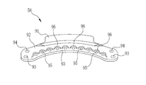
- the support member 58 is a member for supporting the coil spring 57, and has a base end portion 91 having a surface that protrudes most toward the base 51, and the camera body 11 more than the base end portion 91. It is formed in a three-stage shape with a central portion 92 protruding to the back side and a concave portion 93 formed in the central portion 92.
- the base end portion 91 sandwiches the convex portion 74 of the base 51 and the flexible printed circuit board 56.
- the center portion 92 is provided with a first hole portion 93 and a second hole portion 94 through which the screw 63 passes, and the locking pin 62 of the base 51 is inserted into the first hole portion 93.
- the support member 58 is locked to the base 51 and positioned.
- a screw 63 is inserted into the second hole portion 94, and the screw 63 is fastened to the screw hole 64 of the base 51, whereby the support member 58 is fixed to the base 51.
- holes 95 are provided in the vicinity of the central portion 92 at positions corresponding to the contact members 53.
- the hole 95 is a through hole for the assembly jig 102 used when assembling the electrical contact device 33.
- the diameter of the hole 95 is at least smaller than that of the coil spring 57 so that the coil spring 57 does not jump out of the hole 95.
- the assembling jig 102 is provided with shafts 103 arranged in accordance with the arrangement of the holes 95, and each shaft 103 is inserted into the corresponding hole 95.
- the support member 58 is attached to the base 51 in a state where the coil spring 57 is disposed on each shaft 103 protruding from the hole 95.
- a semi-cylindrical guide groove 96 (second groove) is formed at a position corresponding to the contact member 53 and the hole 95 at the boundary between the concave portion 93 and the central portion 92.
- the guide groove 96 together with the guide groove 71 provided in the base 51, forms a guide portion 99 (see FIG. 9) that guides the expansion and contraction of the coil spring 57 along the direction perpendicular to the surface of the base 51.
- the guide groove 96 is formed so as to surround a part of the coil spring 57 from the end on the support member 58 side to the end on the base 51 side. This is because a space in which the flexible printed circuit board 56 is displaced is provided between the base 51 and the support member 58.
- the contact member 53 is inserted into the hole 72, The contact member 53, the flexible printed circuit board 56, and the coil spring 57 are sandwiched between the base 51 and the support member 58 in this order.
- the flexible printed circuit board 56 is inserted between the guide groove 96 and the base 51 between the contact member 53 and the coil spring 57 through the space formed by the concave portion 73 of the base 51 and the central portion 92 of the support member 58.
- the hole 95 is provided at the center of the guide grooves 71 and 96 that surround the outer periphery of the coil spring 57 on the support member 58 side.
- the coil spring 57 has elasticity to expand and contract between an end (one end side) on the base 51 side and an end (other end side) on the support member 58 side, with the other end side supported by the support member 58 as a base point.
- the terminal portion 79 of the flexible printed circuit board 56 is urged at the end on the base 51 side, thereby contacting the base end portion 53b of the contact member 53. Thereby, the conductive pattern 76 exposed to the terminal portion 79 and the contact member 53 are electrically connected.
- the guide groove 71 of the base 51 and the guide groove 96 of the support member 58 form a guide part 99.
- the guide part 99 guides the expansion and contraction of the coil spring 57. That is, the guide part 99 surrounds the outer periphery of the coil spring 57, thereby supporting the coil spring 57 from the side and suppressing the wobbling of the coil spring 57 and the bending at the middle.
- the contact member 53 when the lens unit 12 is attached to the camera body 11, when the contact member 53 is pushed from the front side of the base 51 by the lens unit 12, the coil spring 57 is contracted and the contact member 53 is a hole. It is displaced along the direction of the retracted position along 72. Further, since a space is formed between the base 51 and the support member 58 so that the arm portion 77 of the flexible printed circuit board 56 is displaced by the recess 73 of the base 51 and the central portion 92 of the support member 58, the contact member Even when 53 is displaced to the retracted position (or the protruding position in FIG. 9), the flexible printed circuit board 56 can be displaced without being caught by the base 51 or the support member 58 and is always held between the contact member 53 and the coil spring 57. Can be maintained.
- the electrical contact device 33 forms the guide portion 99 by the guide groove 71 of the base 51 and the guide groove 96 of the support member 58, and guides the expansion and contraction of the coil spring 57 by the guide portion 99.
- the distance from 53 to the side surface of the lens unit 12 can be shortened.
- the position of the contact member 53 is usually determined for compatibility with the replacement lens unit, the distance from the contact member 53 to the side surface of the lens unit 12 is shortened using the electrical contact device 33.
- the space for inserting the lens unit 12 is widened, the diameter of the lens 14 usable in the lens unit 12 is expanded, and the degree of freedom in lens design of the lens unit 12 is improved.
- the electrical contact device 33 (FIG. 11A) is compared with the electrical contact device 111 (FIG. 11B) of the comparative example in which the coil spring 57 is supported only by the support member 58.
- the electrical contact device 111 of the comparative example uses a support member 112 in which a recess 113 for supporting the coil spring 57 is formed at a position corresponding to the guide portion 99 of the electrical contact device 33, and other than that is the same as the electrical contact device 33. Formed.
- the wall 114 is formed between the coil spring 57 and the base 51 in the recess 113 of the electrical contact device 111, the thickness of the wall 114 is approximately between the coil spring 57 and the side wall of the base 51. A gap is generated.
- the guide portion 99 is formed by the base 51 and the guide grooves 71 and 96 of the support member 58, and the coil spring 57 is guided by the guide portion 99. There is almost no gap between the side wall of the base 51. Therefore, as indicated by arrows D1 and D2 in FIGS. 11A and 11B, the electrical contact device 33 is inserted from the contact member 53 to the side surface (inserted) of the electrical contact device 111 of the comparative example.
- the distance to the side surface of the lens unit 12 is generally shorter by the side wall 114 (D1 ⁇ D2).
- the electrical contact device 111 of the comparative example since there is a large gap on the side of the coil spring 57, when the contact member 53 is displaced between the protruding position and the retracted position, the coil spring 57 does not expand and contract straight, May be bent. In this case, the urging force and urging direction of the flexible printed circuit board 56 due to the coil spring 57 may become uneven, and a gap may be formed between the flexible printed circuit board 56 and the contact member 53, and the contact may become unstable. . However, in the electrical contact device 33, about half a circumference of the coil spring 57 is guided by the guide groove 71, and the posture of the coil spring 57 is maintained. Therefore, the coil spring 57 is prevented from being bent at least in the direction of the base 51, and the flexible printed circuit board 56 is used. And the contact member 53 can be contacted stably.
- the contact surface of the contact member 53 and the flexible printed circuit board 56 that is, the surface of the base end part 53 b is made flat, the surface of the base end part 53 b and the flexible printed circuit board 56 are caused by the deflection or inclination of the flexible printed circuit board 56.
- the electrical connection may become unstable due to a gap between the two.
- the surface where the contact member 53 and the flexible printed circuit board 56 are in contact that is, the surface 121 of the base end portion 53 b is formed in a convex curved shape protruding in the direction of the flexible printed circuit board 56. Is preferred.
- the flexible printed circuit board 56 bends in advance along the surface shape of the base end portion 53b, and indefinite temporary bending hardly occurs, and even if a slight inclination occurs, the contact member 53 and the flexible printed circuit board 56 It is easy to touch the surface. For this reason, the electrical connection is stabilized.
- a concave portion 122 is provided at the center of the base end portion 53b having a convex shape, for example. If the recess 122 is provided in this way, the biasing force of the coil spring 57 is concentrated on the edge portion of the recess 122 and the flexible printed board 56 is easily bent along the surface shape of the base end portion 53b. It is easy to stabilize the connection.
- the support member 58 is provided with a hole 95 through which the shaft 103 of the assembly jig 102 passes, but as shown in FIG. 13, a projection 132 corresponding to the shaft 103 of the assembly jig 102 is provided.
- a support member 131 that locks the coil spring 57 by the portion 132 may be used instead of the support member 58. If this support member 131 is used, the electrical contact device 33 can be easily assembled without using the assembly jig 102.
- the electrical contact device 33 is provided on the camera body 11 side
- the electrical contact device 43 on the lens unit side may be an electrical contact device having the same structure as the electrical contact device 33.
- the contact on the camera body 11 side is preferably an electrical contact device that exposes a simple contact.
- the support member 58 includes an arrangement region 141 in which the contact member 53, the hole 72 of the base 51 into which the contact member 53 is inserted, the coil spring 57, and the hole 95 of the support member 58 are arranged. It is fixed to the base 51 with two screws 63 sandwiched in one direction.
- the arrangement of the screws 63 for fixing the support member 58 to the base 51 is preferably determined so that a straight line 142 connecting these screws 63 passes through the arrangement region 141.
- the force for urging each contact member 53 can be made uniform.
- the support member 58 may be fixed to the base 51 at three or more locations. In this case, the arrangement of the fixed portions may be determined so that the center of load at which the coil spring 57 presses the support member 58 passes through the center of gravity of all the fixed portions.
- the support member 58 may be fixed to the base 51 using something other than the screw 63, a locking structure, or a fitting structure.
- the support member 58 is preferably made of a transparent material. If the support member 58 is transparent, the state of the contact member 53, the flexible printed board 56, and the coil spring 57 sandwiched between the base 51 and the support member 58 can be confirmed through the support member 58 when the electrical contact device 33 is assembled. It is easy.
- the coil spring 57 is used to urge the flexible printed circuit board 56 toward the contact member 53.
- another urging member such as a leaf spring may be used.
- the electrical contact device 33 can be suitably used for any device that requires electrical connection to the part to be attached or detached, in addition to the electrical connection between the camera body 11 and the lens unit 12.
Landscapes
- Engineering & Computer Science (AREA)
- Multimedia (AREA)
- Signal Processing (AREA)
- Physics & Mathematics (AREA)
- General Physics & Mathematics (AREA)
- Camera Bodies And Camera Details Or Accessories (AREA)
- Lens Barrels (AREA)
- Structure And Mechanism Of Cameras (AREA)
- Studio Devices (AREA)
Abstract
Priority Applications (3)
| Application Number | Priority Date | Filing Date | Title |
|---|---|---|---|
| JP2015522721A JP5902352B2 (ja) | 2013-06-21 | 2014-06-03 | 電気接点装置、レンズユニット、撮像装置 |
| CN201480034037.4A CN105308501B (zh) | 2013-06-21 | 2014-06-03 | 电接点装置、透镜单元、摄像装置 |
| US14/957,326 US9709875B2 (en) | 2013-06-21 | 2015-12-02 | Electric contact device, lens unit, and imaging device |
Applications Claiming Priority (2)
| Application Number | Priority Date | Filing Date | Title |
|---|---|---|---|
| JP2013-131148 | 2013-06-21 | ||
| JP2013131148 | 2013-06-21 |
Related Child Applications (1)
| Application Number | Title | Priority Date | Filing Date |
|---|---|---|---|
| US14/957,326 Continuation US9709875B2 (en) | 2013-06-21 | 2015-12-02 | Electric contact device, lens unit, and imaging device |
Publications (1)
| Publication Number | Publication Date |
|---|---|
| WO2014203724A1 true WO2014203724A1 (fr) | 2014-12-24 |
Family
ID=52104465
Family Applications (1)
| Application Number | Title | Priority Date | Filing Date |
|---|---|---|---|
| PCT/JP2014/064704 Ceased WO2014203724A1 (fr) | 2013-06-21 | 2014-06-03 | Dispositif de contact électrique, unité de lentille, et dispositif d'imagerie |
Country Status (4)
| Country | Link |
|---|---|
| US (1) | US9709875B2 (fr) |
| JP (1) | JP5902352B2 (fr) |
| CN (1) | CN105308501B (fr) |
| WO (1) | WO2014203724A1 (fr) |
Cited By (1)
| Publication number | Priority date | Publication date | Assignee | Title |
|---|---|---|---|---|
| CN113709965A (zh) * | 2015-07-30 | 2021-11-26 | Lg伊诺特有限公司 | 基板单元和基板组件以及使用其的摄像头模块 |
Families Citing this family (17)
| Publication number | Priority date | Publication date | Assignee | Title |
|---|---|---|---|---|
| USD815678S1 (en) | 2016-03-10 | 2018-04-17 | Fujifilm Corporation | Lens for camera |
| USD831093S1 (en) * | 2016-08-31 | 2018-10-16 | Fujifilm Corporation | Camera lens |
| JP6838928B2 (ja) * | 2016-10-18 | 2021-03-03 | キヤノン株式会社 | 撮像装置およびマウントアダプタ |
| RU2755029C2 (ru) | 2017-05-31 | 2021-09-10 | Кэнон Кабусики Кайся | Аксессуар, устройство захвата изображений, на котором он может устанавливаться, и система камеры |
| US10613419B2 (en) | 2017-05-31 | 2020-04-07 | Canon Kabushiki Kaisha | Imaging apparatus and accessory |
| EP3637184B1 (fr) | 2017-05-31 | 2021-12-15 | Canon Kabushiki Kaisha | Accessoire, appareil de capture d'image sur lequel celui-ci est montable, et systeme de camera |
| CN208401979U (zh) * | 2017-05-31 | 2019-01-18 | 佳能株式会社 | 摄像设备和配件 |
| TWI771631B (zh) * | 2017-05-31 | 2022-07-21 | 日商佳能股份有限公司 | 安裝設備及用於成像設備的配件 |
| US10627704B2 (en) | 2017-05-31 | 2020-04-21 | Canon Kabushiki Kaisha | Accessory, image pickup apparatus on which same is mountable, and camera system |
| SG10202103518RA (en) | 2017-05-31 | 2021-05-28 | Canon Kk | Adapter device, imaging apparatus, and accessory |
| RU2724453C2 (ru) | 2017-05-31 | 2020-06-23 | Кэнон Кабусики Кайся | Устройство объектива, устройство захвата изображений, на котором может устанавливаться устройство объектива, и система камеры |
| CN107656409A (zh) * | 2017-10-23 | 2018-02-02 | 浙江大华技术股份有限公司 | 一种镜头卡口及摄像装置 |
| DE102019107573A1 (de) * | 2019-03-25 | 2020-10-01 | Harting Electric Gmbh & Co. Kg | Steckverbinder |
| JP7325257B2 (ja) * | 2019-08-09 | 2023-08-14 | ニデックインスツルメンツ株式会社 | 振れ補正機能付き光学ユニット |
| CN112787136A (zh) * | 2021-01-27 | 2021-05-11 | 宁波舜宇红外技术有限公司 | 一种镜头通电结构 |
| DE102022202777B3 (de) * | 2022-03-22 | 2023-06-07 | Robert Bosch Gesellschaft mit beschränkter Haftung | Verfahren zur Herstellung einer Kameravorrichtung und Kameravorrichtung für ein Fahrzeug |
| CN116560166B (zh) * | 2023-05-10 | 2025-12-02 | 深圳市永诺电器有限公司 | 一种相机配件及相机系统 |
Citations (11)
| Publication number | Priority date | Publication date | Assignee | Title |
|---|---|---|---|---|
| JPS61147240A (ja) * | 1984-12-20 | 1986-07-04 | Tokinaa Kogaku Kk | 二種類のカメラに対する切換接点を備えた交換レンズ |
| JPH01120135U (fr) * | 1988-02-05 | 1989-08-15 | ||
| JPH02222934A (ja) * | 1988-12-05 | 1990-09-05 | Canon Inc | 光学機器 |
| JPH0467662A (ja) * | 1990-07-09 | 1992-03-03 | Seiko Instr Inc | パッケージリードピン |
| JPH1051117A (ja) * | 1996-07-31 | 1998-02-20 | Nippon Seiki Co Ltd | 通電ピンの固定構造 |
| JPH11327022A (ja) * | 1998-05-19 | 1999-11-26 | Sigma Corp | 交換レンズ用電気コネクター及び接点ピンの組み付け方法 |
| JP2002063728A (ja) * | 2000-08-15 | 2002-02-28 | Yamaha Corp | 光ピックアップ装置用光学部材の取付方法、光ピックアップ装置用ハーフミラーの取付方法、光ピックアップ装置および光ピックアップ装置用ハーフミラー |
| JP2004191689A (ja) * | 2002-12-12 | 2004-07-08 | Pentax Corp | 接点ピン構造 |
| JP2004267351A (ja) * | 2003-03-06 | 2004-09-30 | Olympus Corp | 撮像装置 |
| JP2009288336A (ja) * | 2008-05-27 | 2009-12-10 | Mitsui Seimitsu Kk | 電気的コネクタ、カメラレンズ及びカメラ |
| JP2010134449A (ja) * | 2008-10-30 | 2010-06-17 | Panasonic Corp | カメラボディ、交換レンズユニット、撮像装置 |
Family Cites Families (7)
| Publication number | Priority date | Publication date | Assignee | Title |
|---|---|---|---|---|
| JPS56126627U (fr) * | 1980-02-26 | 1981-09-26 | ||
| JPS6241307Y2 (fr) * | 1981-05-01 | 1987-10-22 | ||
| JPS59152424A (ja) * | 1983-02-18 | 1984-08-31 | Canon Inc | カメラと附属品間の電気信号を授受する電気信号授受装置 |
| JPS60243643A (ja) * | 1984-05-18 | 1985-12-03 | Asahi Optical Co Ltd | 撮影レンズの情報伝達用電気接点構造 |
| US5177520A (en) | 1988-12-05 | 1993-01-05 | Canon Kabushiki Kaisha | Optical apparatus |
| JPH06294990A (ja) | 1993-04-08 | 1994-10-21 | Olympus Optical Co Ltd | カメラのプリント基板実装構造 |
| JP5234188B2 (ja) * | 2010-01-14 | 2013-07-10 | パナソニック株式会社 | デジタルカメラおよび交換レンズユニット |
-
2014
- 2014-06-03 WO PCT/JP2014/064704 patent/WO2014203724A1/fr not_active Ceased
- 2014-06-03 JP JP2015522721A patent/JP5902352B2/ja active Active
- 2014-06-03 CN CN201480034037.4A patent/CN105308501B/zh active Active
-
2015
- 2015-12-02 US US14/957,326 patent/US9709875B2/en active Active
Patent Citations (11)
| Publication number | Priority date | Publication date | Assignee | Title |
|---|---|---|---|---|
| JPS61147240A (ja) * | 1984-12-20 | 1986-07-04 | Tokinaa Kogaku Kk | 二種類のカメラに対する切換接点を備えた交換レンズ |
| JPH01120135U (fr) * | 1988-02-05 | 1989-08-15 | ||
| JPH02222934A (ja) * | 1988-12-05 | 1990-09-05 | Canon Inc | 光学機器 |
| JPH0467662A (ja) * | 1990-07-09 | 1992-03-03 | Seiko Instr Inc | パッケージリードピン |
| JPH1051117A (ja) * | 1996-07-31 | 1998-02-20 | Nippon Seiki Co Ltd | 通電ピンの固定構造 |
| JPH11327022A (ja) * | 1998-05-19 | 1999-11-26 | Sigma Corp | 交換レンズ用電気コネクター及び接点ピンの組み付け方法 |
| JP2002063728A (ja) * | 2000-08-15 | 2002-02-28 | Yamaha Corp | 光ピックアップ装置用光学部材の取付方法、光ピックアップ装置用ハーフミラーの取付方法、光ピックアップ装置および光ピックアップ装置用ハーフミラー |
| JP2004191689A (ja) * | 2002-12-12 | 2004-07-08 | Pentax Corp | 接点ピン構造 |
| JP2004267351A (ja) * | 2003-03-06 | 2004-09-30 | Olympus Corp | 撮像装置 |
| JP2009288336A (ja) * | 2008-05-27 | 2009-12-10 | Mitsui Seimitsu Kk | 電気的コネクタ、カメラレンズ及びカメラ |
| JP2010134449A (ja) * | 2008-10-30 | 2010-06-17 | Panasonic Corp | カメラボディ、交換レンズユニット、撮像装置 |
Cited By (2)
| Publication number | Priority date | Publication date | Assignee | Title |
|---|---|---|---|---|
| CN113709965A (zh) * | 2015-07-30 | 2021-11-26 | Lg伊诺特有限公司 | 基板单元和基板组件以及使用其的摄像头模块 |
| CN113709965B (zh) * | 2015-07-30 | 2023-07-21 | Lg伊诺特有限公司 | 基板单元和基板组件以及使用其的摄像头模块 |
Also Published As
| Publication number | Publication date |
|---|---|
| CN105308501A (zh) | 2016-02-03 |
| JP5902352B2 (ja) | 2016-04-13 |
| US20160085138A1 (en) | 2016-03-24 |
| CN105308501B (zh) | 2018-01-16 |
| US9709875B2 (en) | 2017-07-18 |
| JPWO2014203724A1 (ja) | 2017-02-23 |
Similar Documents
| Publication | Publication Date | Title |
|---|---|---|
| JP5902352B2 (ja) | 電気接点装置、レンズユニット、撮像装置 | |
| US8314878B2 (en) | Image pickup apparatus with impact resistance | |
| CN103748492A (zh) | 透镜镜筒 | |
| JP2024026838A (ja) | 光学装置及び撮像装置 | |
| US11599012B2 (en) | Connecting device of accessory that is detachably attached to accessory shoe device of electronic apparatus, accessory, accessory connecting mechanism, and electronic apparatus system | |
| JP4296134B2 (ja) | カメラモジュールおよび電子機器 | |
| JP5534886B2 (ja) | 電気的コネクタ、カメラレンズ及びカメラ | |
| JP4901811B2 (ja) | 電気的コネクタ、カメラレンズ及びカメラ | |
| US20250102888A1 (en) | Optical apparatus | |
| JP4199799B2 (ja) | レンズユニット | |
| JP2005107217A (ja) | 電子機器 | |
| JP2018141827A (ja) | レンズ鏡筒 | |
| JP6448198B2 (ja) | 電子装置および光学機器 | |
| TWI706210B (zh) | 相機模組以及電子裝置 | |
| JP2011155587A (ja) | 撮像装置 | |
| JP2009300926A (ja) | カメラアクセサリ及びカメラシステム | |
| JP2017106950A (ja) | レンズ鏡筒および光学機器 | |
| US12560820B2 (en) | Optical image stabilization unit capable of being miniaturized, lens barrel, and optical apparatus | |
| US20260099081A1 (en) | Optical apparatus | |
| JP7542963B2 (ja) | 光学機器、カメラシステム | |
| JP2024110638A (ja) | コネクタ及び電子機器 | |
| JP2008225430A (ja) | レンズ鏡筒ユニット | |
| JP2007241103A (ja) | 撮像装置およびレンズ装置 | |
| JP2007017681A (ja) | 鏡胴間部材の固定方法およびレンズユニット並びに撮像装置 | |
| JP2023043940A (ja) | レンズ鏡筒及び撮像装置 |
Legal Events
| Date | Code | Title | Description |
|---|---|---|---|
| WWE | Wipo information: entry into national phase |
Ref document number: 201480034037.4 Country of ref document: CN |
|
| 121 | Ep: the epo has been informed by wipo that ep was designated in this application |
Ref document number: 14814391 Country of ref document: EP Kind code of ref document: A1 |
|
| DPE1 | Request for preliminary examination filed after expiration of 19th month from priority date (pct application filed from 20040101) | ||
| ENP | Entry into the national phase |
Ref document number: 2015522721 Country of ref document: JP Kind code of ref document: A |
|
| NENP | Non-entry into the national phase |
Ref country code: DE |
|
| 122 | Ep: pct application non-entry in european phase |
Ref document number: 14814391 Country of ref document: EP Kind code of ref document: A1 |