WO2014203982A1 - 無線通信装置 - Google Patents
無線通信装置 Download PDFInfo
- Publication number
- WO2014203982A1 WO2014203982A1 PCT/JP2014/066363 JP2014066363W WO2014203982A1 WO 2014203982 A1 WO2014203982 A1 WO 2014203982A1 JP 2014066363 W JP2014066363 W JP 2014066363W WO 2014203982 A1 WO2014203982 A1 WO 2014203982A1
- Authority
- WO
- WIPO (PCT)
- Prior art keywords
- antenna
- conductor
- wireless communication
- notch
- adjacent
- Prior art date
- Legal status (The legal status is an assumption and is not a legal conclusion. Google has not performed a legal analysis and makes no representation as to the accuracy of the status listed.)
- Ceased
Links
Images


Classifications
-
- H—ELECTRICITY
- H04—ELECTRIC COMMUNICATION TECHNIQUE
- H04M—TELEPHONIC COMMUNICATION
- H04M1/00—Substation equipment, e.g. for use by subscribers
- H04M1/02—Constructional features of telephone sets
- H04M1/0202—Portable telephone sets, e.g. cordless phones, mobile phones or bar type handsets
- H04M1/026—Details of the structure or mounting of specific components
- H04M1/0274—Details of the structure or mounting of specific components for an electrical connector module
-
- H—ELECTRICITY
- H01—ELECTRIC ELEMENTS
- H01Q—ANTENNAS, i.e. RADIO AERIALS
- H01Q1/00—Details of, or arrangements associated with, antennas
- H01Q1/12—Supports; Mounting means
- H01Q1/22—Supports; Mounting means by structural association with other equipment or articles
- H01Q1/2291—Supports; Mounting means by structural association with other equipment or articles used in Bluetooth® or Wi-Fi® devices of Wireless Local Area Networks [WLAN]
-
- H—ELECTRICITY
- H01—ELECTRIC ELEMENTS
- H01Q—ANTENNAS, i.e. RADIO AERIALS
- H01Q1/00—Details of, or arrangements associated with, antennas
- H01Q1/52—Means for reducing coupling between antennas; Means for reducing coupling between an antenna and another structure
- H01Q1/521—Means for reducing coupling between antennas; Means for reducing coupling between an antenna and another structure reducing the coupling between adjacent antennas
-
- H—ELECTRICITY
- H01—ELECTRIC ELEMENTS
- H01Q—ANTENNAS, i.e. RADIO AERIALS
- H01Q21/00—Antenna arrays or systems
- H01Q21/28—Combinations of substantially independent non-interacting antenna units or systems
-
- H—ELECTRICITY
- H04—ELECTRIC COMMUNICATION TECHNIQUE
- H04B—TRANSMISSION
- H04B1/00—Details of transmission systems, not covered by a single one of groups H04B3/00 - H04B13/00; Details of transmission systems not characterised by the medium used for transmission
- H04B1/38—Transceivers, i.e. devices in which transmitter and receiver form a structural unit and in which at least one part is used for functions of transmitting and receiving
- H04B1/3827—Portable transceivers
Definitions
- the present invention relates to a wireless communication apparatus including a plurality of antennas that use overlapping frequency bands.
- wireless communication apparatuses capable of executing a plurality of types of wireless communication using overlapping frequency bands, such as wireless LAN communication based on the IEEE 802.11 standard and wireless communication based on the Bluetooth (registered trademark) standard.
- a wireless communication device includes a plurality of antennas in order to support a plurality of standards (see, for example, Patent Document 1).
- the present invention has been made in view of the above circumstances, and one of its purposes is to provide a wireless communication apparatus capable of reducing interference between antennas without relatively separating the distances between a plurality of antennas. There is.
- a wireless communication apparatus includes a first antenna, a second antenna, and a planar conductor disposed so as to be adjacent to one of both the first antenna and the second antenna,
- the conductor is formed with a notch extending from an outer edge between a position adjacent to the first antenna and a position adjacent to the second antenna.
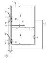
- the wireless communication apparatus 1 is, for example, a portable game machine, a smartphone, or the like, and performs wireless communication using a built-in antenna.
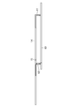
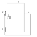
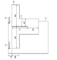
- 1, 2, and 3 are diagrams showing the configuration of main components inside the wireless communication device 1, wherein FIG. 1 is a perspective view, FIG. 2 is a plan view, and FIG. FIG.
- the wireless communication device 1 includes a first antenna 11, a second antenna 12, a main board 13, and a conductor 14.
- the first antenna 11 and the second antenna 12 perform wireless communication using overlapping frequency bands. Specifically, in the present embodiment, the first antenna 11 performs wireless LAN communication based on the IEEE 802.11 standard, and the second antenna 12 performs wireless communication based on the Bluetooth standard. All of these wireless communications are performed using a frequency band of 2.4 GHz.
- the first antenna 11 and the second antenna 12 are both connected to the main board 13 and operate by power feeding from the main board 13.
- a communication module (not shown) is mounted on the main board 13, and this communication module controls the first antenna 11 and the second antenna 12 to transmit and receive radio signals.
- the planar conductor 14 is disposed so as to be adjacent to both the first antenna 11 and the second antenna 12 in order to avoid such interference.
- the conductor 14 is a copper foil having a rectangular shape as a whole, and is attached to one surface of a resin substrate 14a. The substrate 14a is not shown in FIGS.
- the conductor 14 is disposed so as to face the main substrate 13 substantially in parallel, and the first antenna 11 and the second antenna 12 are both disposed on the same side as viewed from the conductor 14.
- the side adjacent to the first antenna 11 and the second antenna 12 is referred to as an adjacent side N.
- the conductor 14 is disposed so that the adjacent side N is parallel to a straight line connecting the first antenna 11 and the second antenna 12.
- the conductor 14 is not in contact with the first antenna 11 and the second antenna 12 and is electrically separated.
- the conductor 14 has a linear notch 15 formed therein.
- the notch 15 is formed to extend from a starting point S located on the adjacent side N in a direction away from both the first antenna 11 and the second antenna 12. Furthermore, the starting point S is located between a region A1 adjacent to the first antenna 11 of the conductor 14 and a region A2 adjacent to the second antenna 12.
- the notch 15 extends toward the center of the conductor 14 along a direction perpendicular to the adjacent side N.
- the length L1 from the starting point S to the innermost part of the notch 15 is preferably determined according to the wavelength ⁇ of the radio wave used by the first antenna 11 and the second antenna 12. More specifically, it is desirable that the length L1 of the notch 15 is determined to be approximately ⁇ / 4. In the case of this embodiment, since the wavelength of the 2.4 GHz frequency radio wave used by the first antenna 11 and the second antenna 12 is about 125 mm, the length L1 of the notch 15 may be about 31 mm.
- the electrical length of the notch part 15 changes according to the dielectric constant. In this case, the length L1 of the notch 15 may be determined so that the electrical length is approximately ⁇ / 4. Therefore, if the substrate 14a is made of a dielectric, the physical length L1 of the notch 15 can be shortened.
- the conductor 14 provided with such a notch 15 so as to be adjacent to both the first antenna 11 and the second antenna 12, a U-shape that flows around the conductor 14 around the notch 15. A current path is formed.
- the notch part resonates with the operating frequency and aggregates the current to reduce current wraparound to the antenna on the other side. Thereby, interference between antennas caused by radio waves flying in the air between the first antenna 11 and the second antenna 12 can be reduced.
- the arrangement position of the conductor 14 and the size of other parts may be determined according to the wavelength ⁇ of the radio wave used by the first antenna 11 and the second antenna 12.
- the distance L2 between the first antenna 11 and the second antenna 12 and the conductor 14 is preferably greater than 0 and not greater than ⁇ / 10.
- the distance W1 between the innermost part of the notch part 15 and the adjacent side N and the opposite side of the conductor 14 is ⁇ / 10 or more.
- the distance W2 from one end of the adjacent side N on the first antenna 11 side to the cutout portion 15 is preferably a length that exceeds the length from the feeding point P1 of the first antenna 11 to the open end.
- the distance W3 from one end of the adjacent side N on the second antenna 12 side to the notch 15 is preferably longer than the length from the feeding point P2 of the second antenna 12 to the open end.
- the conductor 14 may be used not only for reducing interference between antennas but also for other purposes.
- the conductor 14 may be mounted with various circuit elements constituting an electronic circuit, such as a touch sensor, an IC chip, and an NFC resonator.
- the conductor 14 is electrically connected to the main board 13 via the connection portion C shown in FIG. 2 and shares its ground with the main board 13.
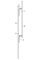
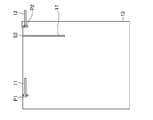
- FIG. 4 is a diagram illustrating a restricted region in the conductor 14 where the connection portion C with the main substrate 13 should not be provided.
- the restricted area is indicated by hatching in FIG.
- the restricted area includes a portion having a width W4 that faces the first antenna 11 and the second antenna 12 along the adjacent side N, and a portion having a width W5 that surrounds the cutout portion 15.
- the width W4 is ⁇ / 10
- W5 is ⁇ / 8.
- the first antenna 11 and the second antenna 12 and the outer edge portion of the conductor 14 are arranged to face each other in order to improve the performance of the conductor 14 to reduce interference between the antennas.
- the conductor 14 is disposed at a position overlapping the first antenna 11 and the second antenna 12 when viewed from the side surface direction (that is, the direction parallel to the surface of the conductor 14).
- the positions of the conductors 14 adjacent to the first antenna 11 and the second antenna 12 are configured so that the thickness thereof is relatively thicker than other portions. Also good.
- a plurality of metal screws 16 are fixed at positions near the regions A1 and A2 of the substrate 14a. As with the substrate 14a, the screw 16 is not shown in FIGS. These screws 16 are configured to come into contact with the copper foil that constitutes the main body of the conductor 14, and constitute a part of the conductor 14. Thereby, the conductor 14 has a thicker portion than the other portions at a position facing the first antenna 11 and the second antenna 12.
- the thickness of the conductor 14 may be increased by providing a through-hole having a metal plating on the inner wall so as to be connected to the conductor 14 body.
- FIG. 5 shows an example in which the position viewed from the side surface direction of the conductor 14 with respect to the first antenna 11 and the second antenna 12 is shifted upward. Even when the conductor 14 is shifted either up or down, the distance L3 along the direction perpendicular to the surface of the conductor 14 from the conductor 14 to each of the first antenna 11 and the second antenna 12 is ⁇ / It is preferable to arrange the conductor 14 so as to be 10 or less.
- the cutout portion 15 is formed in a straight line shape.
- the cutout portion 15 is not limited to such a shape, and for example, has a meandering shape as illustrated in FIG. It may be formed. In this way, the entire length of the cutout portion 15 is secured from the outer edge of the conductor 14 to the innermost portion of the cutout portion 15 while securing a length corresponding to an electrical length of approximately ⁇ / 4 as in FIG. The linear distance can be shortened.
- the length L of the notch 15 may be configured to be changeable.
- the frequency of the radio wave causing the interference also changes depending on which frequency band each antenna uses.
- the frequencies used by these antennas change. Therefore, if the length L of the notch 15 is changed in accordance with the change in frequency, interference in a particularly problematic frequency band can be reduced.
- FIG. 7 shows an example of the structure of the conductor 14 adopting such a method, and two diodes D1 and D2 are arranged in the middle of the notch 15.
- the diode D1 becomes conductive and the effective length of the notch 15 is La in the figure.
- the diode D1 when a voltage is not applied to the diode D1, but a voltage is applied to the diode D2, the diode D1 is electrically cut off and the diode D2 becomes conductive, so that the length of the notch 15 is Lb. Furthermore, in a state where no voltage is applied to both the diodes D1 and D2, the length of the notch 15 is Lc.
- the electrical length of the notch 15 can be changed in a stepwise manner.
- Such on / off control of the diode D is such that a control circuit mounted on the main board 13 outputs a control signal corresponding to the frequency of wireless communication performed by the first antenna 11 and the second antenna 12. Can be realized.
- the length L of the cutout portion 15 is changed in three stages has been shown, but the length L may be changed in two stages using only one diode, or multiple diodes may be arranged in multiple stages. It may be changed to.
- the shape of the conductor 14 is substantially rectangular. However, the shape of the conductor 14 is another shape as long as a current path that goes around the notch 15 can be formed. Also good.
- FIG. 8 shows another example of the shape of the conductor 14.
- the conductor 14 has a portion facing the first antenna 11, a portion facing the second antenna 12, and a U-shape that connects these portions and wraps around through the notch 15. It consists of three parts. Also in the case of this figure, it is preferable that the distances L1, L2, W1, W2, and W3 shown in the figure satisfy the same size requirements as those of the rectangular conductor 14 described above.
- the width W6 of each of the portion facing the first antenna 11 and the portion facing the second antenna 12 is preferably ⁇ / 10 or more.
- the width W7 of the U-shaped part is also preferably ⁇ / 10 or more.
- the notch portion 17 may be formed also in the main board 13.
- FIG. 9 is a diagram showing the configuration of the main board 13 in this case.
- the cutout portion 17 of the main board 13 is for reducing the influence of interference caused by the current flowing between the first antenna 11 and the second antenna 12 via the main board 13. Therefore, the starting point S2 of the notch 17 is located between the position closest to the feeding point P1 of the first antenna 11 and the position closest to the feeding point P2 of the second antenna 12 in the outer edge of the main board 13. Yes.
- the starting point S2 is more preferably located near the midpoint between the point closest to the feeding point P1 on the outer edge of the conductor 14 and the point closest to the feeding point P2.
- the notch part 17 is extended from the starting point S2 so that the position between the 1st antenna 11 and the 2nd antenna 12 may be passed.
- the current flowing on the main board 13 between the first antenna 11 and the second antenna 12 bypasses the notch 17, and interference due to such current occurs. It becomes difficult.
- the notch portion 17 is formed at a position and an orientation that substantially coincide with the notch portion 15 in plan view.
- the length of the notch 17 is determined to be a length corresponding to an electrical length of approximately ⁇ / 4 according to the wavelength of the radio wave transmitted and received by the first antenna 11 and the second antenna 12, similarly to the notch 15. May be.
- the cutout portion 17 may have a different length from the cutout portion 15. By making the lengths of the two different, an effect of reducing interference in a plurality of frequency bands can be obtained without changing the length of each notch.
- the cutout portion 17 is not limited to a linear shape, and may have a meandering shape. Further, the length of the notch 17 may be variable.
- the main body of the conductor 14 is a copper foil formed on the substrate 14a, but other metal foils may be used.
- the conductor 14 may be a metal plate such as an iron plate having a certain thickness.
- the conductor 14 may not be bonded to a substrate formed of an insulator or a dielectric.
- the metal plate may be an exterior cabinet that constitutes a casing of the wireless communication device 1.
- the first antenna 11 and the second antenna 12 may be for performing wireless communication based on a standard other than the wireless LAN or Bluetooth, or may use a frequency band other than 2.4 GHz.
- the wireless communication apparatus includes the first antenna 11, the second antenna 12, the main board 13, and the conductor 14.
- a notch portion 15 is formed.
- the functions of these members are basically the same as in the first embodiment. Therefore, description of the details of the function of each member is omitted.
- the conductor 14 is configured by a bent metal plate, and the substrate 14a is unnecessary.
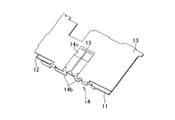
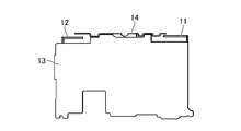
- FIG. 10, FIG. 11, FIG. 12, FIG. 13 and FIG. 14 are diagrams showing the configuration of the main members inside the wireless communication apparatus according to the present embodiment.
- FIG. 10 is a perspective view
- FIG. 12 is a bottom view
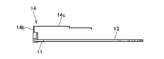
- FIG. 13 is a side view seen from the direction of the solid block arrow in FIG. 11
- FIG. 14 is a side view seen from the direction of the broken block arrow in FIG.
- the first antenna 11 and the second antenna 12 in the present embodiment are arranged so as to protrude in the horizontal direction from one end of the main board 13.
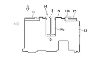
- the conductor 14 is disposed substantially perpendicular to the main substrate 13, is formed by being bent from the adjacent portion 14 b adjacent to the first antenna 11 and the second antenna 12, and from the adjacent portion 14 b, and substantially parallel to the main substrate 13. And a main body portion 14c disposed on the main body 14c.
- the adjacent portion 14b is fixed to the housing of the wireless communication device so as to stand up in a direction substantially perpendicular to the main board 13.
- the adjacent portion 14b is disposed on the side where the first antenna 11 and the second antenna 12 are connected as viewed from the main board 13.
- the conductor 14 is arranged away from the main board 13 without being in direct contact with the main board 13 so as not to be electrically connected to the main board 13.
- the adjacent part 14b is notched at the center by the notch part 15, and is separated into left and right parts, and includes a wing part extending in the left and right directions. The tips of these wings constitute a region A1 adjacent to the first antenna 11 and a region A2 adjacent to the second antenna 12.
- the outer edge on the side where the adjacent portion 14 b is formed in the plan view of the conductor 14 is the adjacent side N.
- the main body portion 14 c extends substantially vertically from the upper end of the adjacent portion 14 b toward the central direction of the main board 13. Further, the main body portion 14c has a U-shape as a whole by forming a notch portion 15 at the center thereof. Similar to the first embodiment, the notch 15 is formed to extend linearly from the starting point S on the adjacent side N toward the center of the main substrate 13 in plan view. Here, the starting point S is located between a region A1 adjacent to the first antenna 11 and a region A2 adjacent to the second antenna 12.
- the conductor 14 provided with the notch 15 is disposed so as to be adjacent to both the first antenna 11 and the second antenna 12 so that the notch 15 is formed.
- a U-shaped current path that wraps around and flows on the conductor 14 is formed.
- the notch part resonates with the operating frequency and aggregates the current to reduce current wraparound to the antenna on the other side. Thereby, interference between antennas caused by radio waves flying in the air between the first antenna 11 and the second antenna 12 can be reduced.
- the conductor 14 is bent at the portion of the adjacent side N, so that the region A1 adjacent to the first antenna 11 and the region A2 adjacent to the second antenna 12 of the conductor 14 are from the main body 14c. It is thick.
- the conductor 14 is bent at the portion of the adjacent side N in this way, so that when the main board 13 and the conductor 14 are viewed from the side, the first antenna 11, the region A 1, and the second antenna 12 The distance between the areas A2 can be reduced.
- FIG. 5 in the first embodiment with respect to the main body portion 14c between the first antenna 11 and the second antenna 12 and the regions A1 and A2 adjacent to each antenna of the conductor 14.
- the distance L3 along the vertical direction is preferably ⁇ / 10 or less.
- the adjacent portion 14b including the regions A1 and A2 is bent with respect to the main body portion 14c, so that the main body portion 14c is disposed at a position somewhat away from the main board 13 but the region A1.
- A2 can be arranged at positions close to the first antenna 11 and the second antenna 12.
Landscapes
- Engineering & Computer Science (AREA)
- Computer Networks & Wireless Communication (AREA)
- Signal Processing (AREA)
- Variable-Direction Aerials And Aerial Arrays (AREA)
- Details Of Aerials (AREA)
Abstract
Description
本発明の第1の実施形態に係る無線通信装置1は、例えば携帯型ゲーム機やスマートフォン等であって、内蔵するアンテナによって無線通信を行う。図1、図2及び図3は、無線通信装置1の内部における主要部品の構成を示す図であって、図1は斜視図、図2は平面図、図3は図2における矢印の方向から見た側面図である。これらの図に示すように、無線通信装置1は、第1アンテナ11と、第2アンテナ12と、メイン基板13と、導電体14と、を含んで構成されている。
以下、本発明の第2の実施形態に係る無線通信装置について、説明する。本実施形態に係る無線通信装置も、第1実施形態と同様に、第1アンテナ11、第2アンテナ12、メイン基板13、及び導電体14を含んで構成されており、導電体14には切り欠き部15が形成されている。これら各部材の機能は、基本的に第1実施形態と同様である。そのため、各部材の機能の詳細については、説明を省略する。本実施形態では、第1実施形態と異なり、導電体14が折り曲げられた金属板によって構成されており、基板14aは不要となっている。
Claims (7)
- 第1アンテナと、
第2アンテナと、
前記第1アンテナ及び第2アンテナの双方と一方側において隣接するように配置された面状の導電体と、
を備え、
前記導電体には、前記第1アンテナに隣接する位置と、前記第2アンテナに隣接する位置との間の外縁から延びる切り欠き部が形成されている
ことを特徴とする無線通信装置。 - 請求項1に記載の無線通信装置において、
前記切り欠き部は、その長さが可変に構成されている
ことを特徴とする無線通信装置。 - 請求項1又は2に記載の無線通信装置において、
前記導電体は、側面方向から見て前記第1アンテナ及び第2アンテナと重なる位置に配置されている
ことを特徴とする無線通信装置。 - 請求項1から3のいずれか一項に記載の無線通信装置において、
前記導電体の、前記第1アンテナ及び第2アンテナと隣接する位置に、他の部分より厚い部分が形成されている
ことを特徴とする無線通信装置。 - 請求項1から4のいずれか一項に記載の無線通信装置において、
前記第1アンテナ及び第2アンテナと接続される基板をさらに備え、
前記基板には、前記第1アンテナが接続される位置と、前記第2アンテナが接続される位置との間を通るように前記基板の外縁から延びる切り欠き部が形成されている
ことを特徴とする無線通信装置。 - 請求項1から5のいずれか一項に記載の無線通信装置において、
前記導電体は、誘電体で形成された基板に接着されている
ことを特徴とする無線通信装置。 - 請求項1から6のいずれか一項に記載の無線通信装置において、
前記導電体は、電子回路を構成する回路素子が搭載された基板に接着されている
ことを特徴とする無線通信装置。
Priority Applications (4)
| Application Number | Priority Date | Filing Date | Title |
|---|---|---|---|
| EP14814394.4A EP3012913B1 (en) | 2013-06-20 | 2014-06-19 | Wireless communication device |
| JP2015522985A JP6046251B2 (ja) | 2013-06-20 | 2014-06-19 | 無線通信装置 |
| US14/896,832 US9621693B2 (en) | 2013-06-20 | 2014-06-19 | Wireless communication device |
| CN201480033088.5A CN105393404B (zh) | 2013-06-20 | 2014-06-19 | 无线通信设备 |
Applications Claiming Priority (2)
| Application Number | Priority Date | Filing Date | Title |
|---|---|---|---|
| JP2013129398 | 2013-06-20 | ||
| JP2013-129398 | 2013-06-20 |
Publications (1)
| Publication Number | Publication Date |
|---|---|
| WO2014203982A1 true WO2014203982A1 (ja) | 2014-12-24 |
Family
ID=52104708
Family Applications (1)
| Application Number | Title | Priority Date | Filing Date |
|---|---|---|---|
| PCT/JP2014/066363 Ceased WO2014203982A1 (ja) | 2013-06-20 | 2014-06-19 | 無線通信装置 |
Country Status (5)
| Country | Link |
|---|---|
| US (1) | US9621693B2 (ja) |
| EP (1) | EP3012913B1 (ja) |
| JP (1) | JP6046251B2 (ja) |
| CN (1) | CN105393404B (ja) |
| WO (1) | WO2014203982A1 (ja) |
Cited By (2)
| Publication number | Priority date | Publication date | Assignee | Title |
|---|---|---|---|---|
| WO2016112617A1 (zh) * | 2015-01-14 | 2016-07-21 | 中兴通讯股份有限公司 | 天线互扰隔离装置、无线网卡及终端 |
| WO2024218985A1 (ja) * | 2023-04-21 | 2024-10-24 | 株式会社ソニー・インタラクティブエンタテインメント | 電子機器 |
Citations (5)
| Publication number | Priority date | Publication date | Assignee | Title |
|---|---|---|---|---|
| JP2004096464A (ja) * | 2002-08-30 | 2004-03-25 | Anten Corp | 周波数共用アンテナ |
| JP2007243455A (ja) * | 2006-03-07 | 2007-09-20 | Yokohama National Univ | 無線受信用小型携帯端末装置 |
| JP2008283464A (ja) * | 2007-05-10 | 2008-11-20 | Toshiba Corp | 電子機器 |
| JP2010041090A (ja) * | 2008-07-31 | 2010-02-18 | Denso Corp | マイクロストリップアレーアンテナ |
| JP2010259048A (ja) | 2009-04-02 | 2010-11-11 | Sony Computer Entertainment Inc | 情報通信装置及びアンテナ |
Family Cites Families (10)
| Publication number | Priority date | Publication date | Assignee | Title |
|---|---|---|---|---|
| US6624789B1 (en) * | 2002-04-11 | 2003-09-23 | Nokia Corporation | Method and system for improving isolation in radio-frequency antennas |
| CN1989652B (zh) * | 2004-06-28 | 2013-03-13 | 脉冲芬兰有限公司 | 天线部件 |
| CN101208831A (zh) * | 2005-06-06 | 2008-06-25 | 松下电器产业株式会社 | 平面天线装置以及使用该平面天线装置的无线通信装置 |
| US7786944B2 (en) * | 2007-10-25 | 2010-08-31 | Motorola, Inc. | High frequency communication device on multilayered substrate |
| ES2455095T3 (es) * | 2008-05-12 | 2014-04-14 | Panasonic Corporation | Aparato de antena |
| JP5223584B2 (ja) * | 2008-10-14 | 2013-06-26 | 富士通モバイルコミュニケーションズ株式会社 | 無線通信装置 |
| TW201021290A (en) * | 2008-11-28 | 2010-06-01 | Asustek Comp Inc | Planar antenna |
| JP5431200B2 (ja) * | 2010-02-10 | 2014-03-05 | シャープ株式会社 | 回路基板、及び当該回路基板を備えた電子機器 |
| US9105975B2 (en) | 2010-05-17 | 2015-08-11 | Panasonic Intellectual Property Management Co., Ltd. | Antenna device and portable wireless terminal equipped with the same |
| JP2012039465A (ja) | 2010-08-09 | 2012-02-23 | Panasonic Corp | 携帯無線機 |
-
2014
- 2014-06-19 US US14/896,832 patent/US9621693B2/en active Active
- 2014-06-19 CN CN201480033088.5A patent/CN105393404B/zh active Active
- 2014-06-19 EP EP14814394.4A patent/EP3012913B1/en active Active
- 2014-06-19 WO PCT/JP2014/066363 patent/WO2014203982A1/ja not_active Ceased
- 2014-06-19 JP JP2015522985A patent/JP6046251B2/ja active Active
Patent Citations (5)
| Publication number | Priority date | Publication date | Assignee | Title |
|---|---|---|---|---|
| JP2004096464A (ja) * | 2002-08-30 | 2004-03-25 | Anten Corp | 周波数共用アンテナ |
| JP2007243455A (ja) * | 2006-03-07 | 2007-09-20 | Yokohama National Univ | 無線受信用小型携帯端末装置 |
| JP2008283464A (ja) * | 2007-05-10 | 2008-11-20 | Toshiba Corp | 電子機器 |
| JP2010041090A (ja) * | 2008-07-31 | 2010-02-18 | Denso Corp | マイクロストリップアレーアンテナ |
| JP2010259048A (ja) | 2009-04-02 | 2010-11-11 | Sony Computer Entertainment Inc | 情報通信装置及びアンテナ |
Cited By (2)
| Publication number | Priority date | Publication date | Assignee | Title |
|---|---|---|---|---|
| WO2016112617A1 (zh) * | 2015-01-14 | 2016-07-21 | 中兴通讯股份有限公司 | 天线互扰隔离装置、无线网卡及终端 |
| WO2024218985A1 (ja) * | 2023-04-21 | 2024-10-24 | 株式会社ソニー・インタラクティブエンタテインメント | 電子機器 |
Also Published As
| Publication number | Publication date |
|---|---|
| EP3012913A4 (en) | 2017-02-22 |
| US9621693B2 (en) | 2017-04-11 |
| US20160134731A1 (en) | 2016-05-12 |
| CN105393404B (zh) | 2019-02-01 |
| JP6046251B2 (ja) | 2016-12-14 |
| CN105393404A (zh) | 2016-03-09 |
| JPWO2014203982A1 (ja) | 2017-02-23 |
| EP3012913A1 (en) | 2016-04-27 |
| EP3012913B1 (en) | 2021-03-17 |
Similar Documents
| Publication | Publication Date | Title |
|---|---|---|
| CN113517556B (zh) | 天线结构及具有该天线结构的电子设备 | |
| JP6222103B2 (ja) | アンテナ及び無線通信装置 | |
| CN105474458B (zh) | 计算设备外壳中的背面天线 | |
| CN106921021A (zh) | 一种天线结构及电子设备 | |
| US12494586B2 (en) | Integrated multiple-antenna configuration and antenna module | |
| JP2010068085A (ja) | アンテナ装置 | |
| WO2010109771A1 (ja) | 携帯無線端末 | |
| WO2014132519A1 (ja) | アンテナ、プリント基板、及び無線通信装置 | |
| KR101003014B1 (ko) | 칩 안테나를 위한 pcb 레이아웃 구조 및 이를 이용한 칩 안테나 장치 | |
| US9385425B2 (en) | Antenna device | |
| JPWO2013145623A1 (ja) | アンテナ装置およびそれを搭載した携帯無線機器 | |
| JP2015062276A (ja) | アンテナ | |
| JP5900660B2 (ja) | Mimoアンテナおよび無線装置 | |
| WO2011016160A1 (ja) | 携帯無線機 | |
| JP5933631B2 (ja) | アンテナアセンブリ | |
| JP6046251B2 (ja) | 無線通信装置 | |
| JP6233319B2 (ja) | マルチバンドアンテナ及び無線装置 | |
| JP5404888B1 (ja) | アンテナ装置を備えた電子機器 | |
| US12046814B2 (en) | Antenna unit and communication equipment | |
| JP2019016838A (ja) | アンテナ装置 | |
| CN205069829U (zh) | 联接结构、通讯结构和逆变器 | |
| JP5598761B2 (ja) | アンテナ及びそれを備えた無線装置 | |
| JP6865072B2 (ja) | アンテナ装置及びアンテナ装置を備えた電子機器 | |
| JP5526736B2 (ja) | スロットアンテナ及びこれを備えている無線通信端末 | |
| JP2009171089A (ja) | アンテナ |
Legal Events
| Date | Code | Title | Description |
|---|---|---|---|
| WWE | Wipo information: entry into national phase |
Ref document number: 201480033088.5 Country of ref document: CN |
|
| 121 | Ep: the epo has been informed by wipo that ep was designated in this application |
Ref document number: 14814394 Country of ref document: EP Kind code of ref document: A1 |
|
| WWE | Wipo information: entry into national phase |
Ref document number: 2014814394 Country of ref document: EP |
|
| WWE | Wipo information: entry into national phase |
Ref document number: 14896832 Country of ref document: US |
|
| ENP | Entry into the national phase |
Ref document number: 2015522985 Country of ref document: JP Kind code of ref document: A |
|
| NENP | Non-entry into the national phase |
Ref country code: DE |