WO2014208324A1 - 膜形成用組成物、レジスト下層膜及びその形成方法、パターン形成方法並びに化合物 - Google Patents
膜形成用組成物、レジスト下層膜及びその形成方法、パターン形成方法並びに化合物 Download PDFInfo
- Publication number
- WO2014208324A1 WO2014208324A1 PCT/JP2014/065265 JP2014065265W WO2014208324A1 WO 2014208324 A1 WO2014208324 A1 WO 2014208324A1 JP 2014065265 W JP2014065265 W JP 2014065265W WO 2014208324 A1 WO2014208324 A1 WO 2014208324A1
- Authority
- WO
- WIPO (PCT)
- Prior art keywords
- group
- film
- resist underlayer
- compound
- underlayer film
- Prior art date
- Legal status (The legal status is an assumption and is not a legal conclusion. Google has not performed a legal analysis and makes no representation as to the accuracy of the status listed.)
- Ceased
Links
- BCLPTSGSECCKHV-UHFFFAOYSA-N C#Cc(cc1)ccc1-c(cc1)ccc1-c(c(O)c(-c(cc1)ccc1-c(cc1)ccc1C#C)c(O)c1-c(cc2)ccc2-c(cc2)ccc2C#C)c1O Chemical compound C#Cc(cc1)ccc1-c(cc1)ccc1-c(c(O)c(-c(cc1)ccc1-c(cc1)ccc1C#C)c(O)c1-c(cc2)ccc2-c(cc2)ccc2C#C)c1O BCLPTSGSECCKHV-UHFFFAOYSA-N 0.000 description 1
- 0 CC1(C=CC(c2cc(-c(cc3)ccc3C#CC)cc(-c(cc3)ccc3C#C*)c2)=CC1)C#* Chemical compound CC1(C=CC(c2cc(-c(cc3)ccc3C#CC)cc(-c(cc3)ccc3C#C*)c2)=CC1)C#* 0.000 description 1
- IKTZHUAHYNPMNQ-UHFFFAOYSA-N Nc1cc(C#Cc(cc2)ccc2-c2cc(-c(cc3)ccc3C#Cc3cccc(N)c3)cc(-c(cc3)ccc3C#Cc3cccc(N)c3)c2)ccc1 Chemical compound Nc1cc(C#Cc(cc2)ccc2-c2cc(-c(cc3)ccc3C#Cc3cccc(N)c3)cc(-c(cc3)ccc3C#Cc3cccc(N)c3)c2)ccc1 IKTZHUAHYNPMNQ-UHFFFAOYSA-N 0.000 description 1
- NTJWCPHKDNYOGR-UHFFFAOYSA-N OCC#Cc(cc1)ccc1-c1cc(-c(cc2)ccc2C#CCO)cc(-c(cc2)ccc2C#CCO)c1 Chemical compound OCC#Cc(cc1)ccc1-c1cc(-c(cc2)ccc2C#CCO)cc(-c(cc2)ccc2C#CCO)c1 NTJWCPHKDNYOGR-UHFFFAOYSA-N 0.000 description 1
Classifications
-
- G—PHYSICS
- G03—PHOTOGRAPHY; CINEMATOGRAPHY; ANALOGOUS TECHNIQUES USING WAVES OTHER THAN OPTICAL WAVES; ELECTROGRAPHY; HOLOGRAPHY
- G03F—PHOTOMECHANICAL PRODUCTION OF TEXTURED OR PATTERNED SURFACES, e.g. FOR PRINTING, FOR PROCESSING OF SEMICONDUCTOR DEVICES; MATERIALS THEREFOR; ORIGINALS THEREFOR; APPARATUS SPECIALLY ADAPTED THEREFOR
- G03F7/00—Photomechanical, e.g. photolithographic, production of textured or patterned surfaces, e.g. printing surfaces; Materials therefor, e.g. comprising photoresists; Apparatus specially adapted therefor
- G03F7/004—Photosensitive materials
- G03F7/09—Photosensitive materials characterised by structural details, e.g. supports, auxiliary layers
- G03F7/11—Photosensitive materials characterised by structural details, e.g. supports, auxiliary layers having cover layers or intermediate layers, e.g. subbing layers
-
- C—CHEMISTRY; METALLURGY
- C07—ORGANIC CHEMISTRY
- C07C—ACYCLIC OR CARBOCYCLIC COMPOUNDS
- C07C15/00—Cyclic hydrocarbons containing only six-membered aromatic rings as cyclic parts
- C07C15/12—Polycyclic non-condensed hydrocarbons
- C07C15/14—Polycyclic non-condensed hydrocarbons all phenyl groups being directly linked
-
- C—CHEMISTRY; METALLURGY
- C07—ORGANIC CHEMISTRY
- C07C—ACYCLIC OR CARBOCYCLIC COMPOUNDS
- C07C15/00—Cyclic hydrocarbons containing only six-membered aromatic rings as cyclic parts
- C07C15/12—Polycyclic non-condensed hydrocarbons
- C07C15/18—Polycyclic non-condensed hydrocarbons containing at least one group with formula
-
- C—CHEMISTRY; METALLURGY
- C07—ORGANIC CHEMISTRY
- C07C—ACYCLIC OR CARBOCYCLIC COMPOUNDS
- C07C15/00—Cyclic hydrocarbons containing only six-membered aromatic rings as cyclic parts
- C07C15/40—Cyclic hydrocarbons containing only six-membered aromatic rings as cyclic parts substituted by unsaturated carbon radicals
- C07C15/50—Cyclic hydrocarbons containing only six-membered aromatic rings as cyclic parts substituted by unsaturated carbon radicals polycyclic non-condensed
-
- C—CHEMISTRY; METALLURGY
- C07—ORGANIC CHEMISTRY
- C07C—ACYCLIC OR CARBOCYCLIC COMPOUNDS
- C07C15/00—Cyclic hydrocarbons containing only six-membered aromatic rings as cyclic parts
- C07C15/40—Cyclic hydrocarbons containing only six-membered aromatic rings as cyclic parts substituted by unsaturated carbon radicals
- C07C15/50—Cyclic hydrocarbons containing only six-membered aromatic rings as cyclic parts substituted by unsaturated carbon radicals polycyclic non-condensed
- C07C15/54—Cyclic hydrocarbons containing only six-membered aromatic rings as cyclic parts substituted by unsaturated carbon radicals polycyclic non-condensed containing a group with formula
-
- C—CHEMISTRY; METALLURGY
- C07—ORGANIC CHEMISTRY
- C07C—ACYCLIC OR CARBOCYCLIC COMPOUNDS
- C07C15/00—Cyclic hydrocarbons containing only six-membered aromatic rings as cyclic parts
- C07C15/40—Cyclic hydrocarbons containing only six-membered aromatic rings as cyclic parts substituted by unsaturated carbon radicals
- C07C15/56—Cyclic hydrocarbons containing only six-membered aromatic rings as cyclic parts substituted by unsaturated carbon radicals polycyclic condensed
- C07C15/58—Cyclic hydrocarbons containing only six-membered aromatic rings as cyclic parts substituted by unsaturated carbon radicals polycyclic condensed containing two rings
-
- C—CHEMISTRY; METALLURGY
- C07—ORGANIC CHEMISTRY
- C07C—ACYCLIC OR CARBOCYCLIC COMPOUNDS
- C07C211/00—Compounds containing amino groups bound to a carbon skeleton
- C07C211/43—Compounds containing amino groups bound to a carbon skeleton having amino groups bound to carbon atoms of six-membered aromatic rings of the carbon skeleton
- C07C211/44—Compounds containing amino groups bound to a carbon skeleton having amino groups bound to carbon atoms of six-membered aromatic rings of the carbon skeleton having amino groups bound to only one six-membered aromatic ring
- C07C211/49—Compounds containing amino groups bound to a carbon skeleton having amino groups bound to carbon atoms of six-membered aromatic rings of the carbon skeleton having amino groups bound to only one six-membered aromatic ring having at least two amino groups bound to the carbon skeleton
- C07C211/50—Compounds containing amino groups bound to a carbon skeleton having amino groups bound to carbon atoms of six-membered aromatic rings of the carbon skeleton having amino groups bound to only one six-membered aromatic ring having at least two amino groups bound to the carbon skeleton with at least two amino groups bound to carbon atoms of six-membered aromatic rings of the carbon skeleton
-
- C—CHEMISTRY; METALLURGY
- C07—ORGANIC CHEMISTRY
- C07C—ACYCLIC OR CARBOCYCLIC COMPOUNDS
- C07C211/00—Compounds containing amino groups bound to a carbon skeleton
- C07C211/43—Compounds containing amino groups bound to a carbon skeleton having amino groups bound to carbon atoms of six-membered aromatic rings of the carbon skeleton
- C07C211/57—Compounds containing amino groups bound to a carbon skeleton having amino groups bound to carbon atoms of six-membered aromatic rings of the carbon skeleton having amino groups bound to carbon atoms of six-membered aromatic rings being part of condensed ring systems of the carbon skeleton
- C07C211/58—Naphthylamines; N-substituted derivatives thereof
-
- C—CHEMISTRY; METALLURGY
- C07—ORGANIC CHEMISTRY
- C07C—ACYCLIC OR CARBOCYCLIC COMPOUNDS
- C07C25/00—Compounds containing at least one halogen atom bound to a six-membered aromatic ring
- C07C25/24—Halogenated aromatic hydrocarbons with unsaturated side chains
-
- C—CHEMISTRY; METALLURGY
- C07—ORGANIC CHEMISTRY
- C07C—ACYCLIC OR CARBOCYCLIC COMPOUNDS
- C07C33/00—Unsaturated compounds having hydroxy or O-metal groups bound to acyclic carbon atoms
- C07C33/28—Alcohols containing only six-membered aromatic rings as cyclic part with unsaturation outside the aromatic rings
-
- C—CHEMISTRY; METALLURGY
- C07—ORGANIC CHEMISTRY
- C07C—ACYCLIC OR CARBOCYCLIC COMPOUNDS
- C07C33/00—Unsaturated compounds having hydroxy or O-metal groups bound to acyclic carbon atoms
- C07C33/38—Alcohols containing six-membered aromatic rings and other rings and having unsaturation outside the aromatic rings
-
- C—CHEMISTRY; METALLURGY
- C07—ORGANIC CHEMISTRY
- C07C—ACYCLIC OR CARBOCYCLIC COMPOUNDS
- C07C39/00—Compounds having at least one hydroxy or O-metal group bound to a carbon atom of a six-membered aromatic ring
- C07C39/205—Compounds having at least one hydroxy or O-metal group bound to a carbon atom of a six-membered aromatic ring polycyclic, containing only six-membered aromatic rings as cyclic parts with unsaturation outside the rings
- C07C39/21—Compounds having at least one hydroxy or O-metal group bound to a carbon atom of a six-membered aromatic ring polycyclic, containing only six-membered aromatic rings as cyclic parts with unsaturation outside the rings with at least one hydroxy group on a non-condensed ring
-
- C—CHEMISTRY; METALLURGY
- C07—ORGANIC CHEMISTRY
- C07C—ACYCLIC OR CARBOCYCLIC COMPOUNDS
- C07C43/00—Ethers; Compounds having groups, groups or groups
- C07C43/02—Ethers
- C07C43/20—Ethers having an ether-oxygen atom bound to a carbon atom of a six-membered aromatic ring
- C07C43/215—Ethers having an ether-oxygen atom bound to a carbon atom of a six-membered aromatic ring having unsaturation outside the six-membered aromatic rings
-
- C—CHEMISTRY; METALLURGY
- C08—ORGANIC MACROMOLECULAR COMPOUNDS; THEIR PREPARATION OR CHEMICAL WORKING-UP; COMPOSITIONS BASED THEREON
- C08F—MACROMOLECULAR COMPOUNDS OBTAINED BY REACTIONS ONLY INVOLVING CARBON-TO-CARBON UNSATURATED BONDS
- C08F38/00—Homopolymers and copolymers of compounds having one or more carbon-to-carbon triple bonds
-
- G—PHYSICS
- G03—PHOTOGRAPHY; CINEMATOGRAPHY; ANALOGOUS TECHNIQUES USING WAVES OTHER THAN OPTICAL WAVES; ELECTROGRAPHY; HOLOGRAPHY
- G03F—PHOTOMECHANICAL PRODUCTION OF TEXTURED OR PATTERNED SURFACES, e.g. FOR PRINTING, FOR PROCESSING OF SEMICONDUCTOR DEVICES; MATERIALS THEREFOR; ORIGINALS THEREFOR; APPARATUS SPECIALLY ADAPTED THEREFOR
- G03F7/00—Photomechanical, e.g. photolithographic, production of textured or patterned surfaces, e.g. printing surfaces; Materials therefor, e.g. comprising photoresists; Apparatus specially adapted therefor
- G03F7/004—Photosensitive materials
- G03F7/09—Photosensitive materials characterised by structural details, e.g. supports, auxiliary layers
- G03F7/094—Multilayer resist systems, e.g. planarising layers
-
- G—PHYSICS
- G03—PHOTOGRAPHY; CINEMATOGRAPHY; ANALOGOUS TECHNIQUES USING WAVES OTHER THAN OPTICAL WAVES; ELECTROGRAPHY; HOLOGRAPHY
- G03F—PHOTOMECHANICAL PRODUCTION OF TEXTURED OR PATTERNED SURFACES, e.g. FOR PRINTING, FOR PROCESSING OF SEMICONDUCTOR DEVICES; MATERIALS THEREFOR; ORIGINALS THEREFOR; APPARATUS SPECIALLY ADAPTED THEREFOR
- G03F7/00—Photomechanical, e.g. photolithographic, production of textured or patterned surfaces, e.g. printing surfaces; Materials therefor, e.g. comprising photoresists; Apparatus specially adapted therefor
- G03F7/16—Coating processes; Apparatus therefor
- G03F7/168—Finishing the coated layer, e.g. drying, baking, soaking
-
- G—PHYSICS
- G03—PHOTOGRAPHY; CINEMATOGRAPHY; ANALOGOUS TECHNIQUES USING WAVES OTHER THAN OPTICAL WAVES; ELECTROGRAPHY; HOLOGRAPHY
- G03F—PHOTOMECHANICAL PRODUCTION OF TEXTURED OR PATTERNED SURFACES, e.g. FOR PRINTING, FOR PROCESSING OF SEMICONDUCTOR DEVICES; MATERIALS THEREFOR; ORIGINALS THEREFOR; APPARATUS SPECIALLY ADAPTED THEREFOR
- G03F7/00—Photomechanical, e.g. photolithographic, production of textured or patterned surfaces, e.g. printing surfaces; Materials therefor, e.g. comprising photoresists; Apparatus specially adapted therefor
- G03F7/26—Processing photosensitive materials; Apparatus therefor
- G03F7/36—Imagewise removal not covered by groups G03F7/30 - G03F7/34, e.g. using gas streams, using plasma
-
- H—ELECTRICITY
- H10—SEMICONDUCTOR DEVICES; ELECTRIC SOLID-STATE DEVICES NOT OTHERWISE PROVIDED FOR
- H10P—GENERIC PROCESSES OR APPARATUS FOR THE MANUFACTURE OR TREATMENT OF DEVICES COVERED BY CLASS H10
- H10P76/00—Manufacture or treatment of masks on semiconductor bodies, e.g. by lithography or photolithography
- H10P76/20—Manufacture or treatment of masks on semiconductor bodies, e.g. by lithography or photolithography of masks comprising organic materials
Definitions
- the present invention relates to a film forming composition, a resist underlayer film, a forming method thereof, a pattern forming method, and a compound.
- a multilayer resist process is used to obtain a high degree of integration.
- a resist underlayer film forming composition is first applied to the upper surface side of a substrate to form a resist underlayer film, and then a resist pattern is formed on the upper surface side of the resist underlayer film. Subsequently, this resist pattern is transferred to the resist underlayer film by etching, and further, a desired pattern can be obtained by transferring this resist underlayer film pattern to the substrate.
- the resist underlayer film used in such a multilayer resist process is required to have general characteristics such as an appropriate refractive index, optical characteristics such as an absorption coefficient, and good etching resistance.
- an inorganic hard mask as an intermediate layer is formed on the resist underlayer film by a CVD method.
- an inorganic hard mask is produced by a CVD method, particularly in the case of a nitride film, heating of the substrate at a minimum of 300 ° C., usually 400 ° C. is required.
- the resist underlayer film formed using the conventional composition has difficulty in heat resistance. Therefore, due to the low heat resistance, the resist underlayer film is heated by the resist underlayer film formation. There is an inconvenience that the components are sublimated, and the sublimated components are reattached to the substrate to deteriorate the manufacturing yield of the semiconductor device.
- the resist underlayer film to be formed is It is required that these trenches are sufficiently buried and have high flatness. As described above, various characteristics are required for the resist underlayer film, but the conventional resist underlayer film forming composition cannot satisfy these requirements.
- the present invention has been made based on the circumstances as described above, and the purpose thereof is to form a resist underlayer film that sufficiently satisfies general characteristics such as optical characteristics and etching resistance and has high heat resistance and high flatness. It is providing the composition for film formation.
- R 1, R 2 and R 3 is a group represented by the following formula (a) .R 1, R 2 and R 3, which may be the same or different .R a , R b , R c, and R d are each independently a halogen atom, a hydroxy group, an amino group, a sulfanyl group, or a monovalent organic group having 1 to 20 carbon atoms that does not contain an aromatic ring.
- R A is a hydrogen atom, an aryl group, or an alkyl group substituted or unsubstituted with at least one of a hydroxy group and an aryl group.
- R B is a single bond or an arylene group.
- Some or all of the hydrogen atoms on the aromatic ring of the aryl group and arylene group are halogen atoms, hydroxy groups, amino groups, sulfanyl groups, or monovalent organic groups having 1 to 20 carbon atoms that do not contain an aromatic ring. May be substituted with.
- Another invention made to solve the above problems is a resist underlayer film formed from the film forming composition.
- Still another invention made in order to solve the above-mentioned problems comprises a step of forming a coating film on the upper surface side of the substrate and a step of baking the coating film, and the coating film is formed from the film-forming composition.
- This is a method for forming a resist underlayer film.
- Still another invention made to solve the above-described problems includes a step of forming a resist pattern on the upper surface side of the resist underlayer film, and a step of sequentially etching the resist underlayer film and the substrate using the resist pattern as a mask. And a pattern forming method in which the resist underlayer film is formed by a method of forming the resist underlayer film.
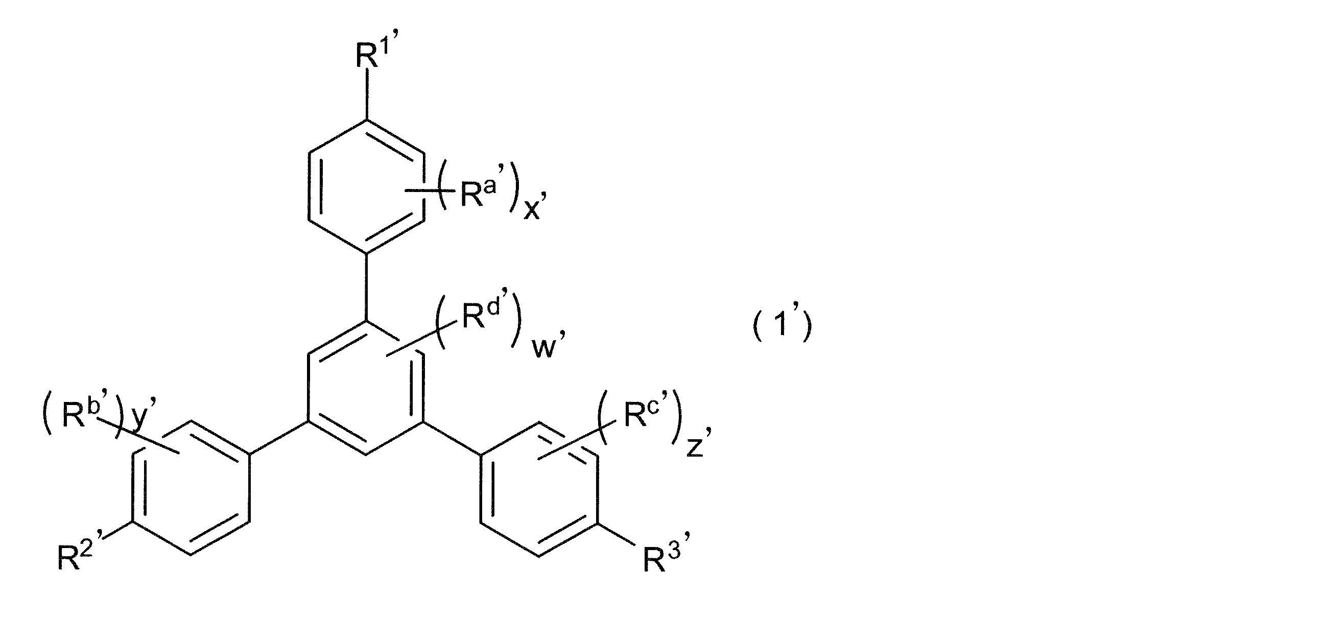
- Still another invention made to solve the above problems is a compound represented by the following formula (1 ').
- R 1 , R 2 and R 3 are groups represented by the following Formula (a ′).
- R 1 , R 2 and R 3 may be the same or different.
- R a ′ , R b ′ , R c ′, and R d ′ each independently represent a halogen atom, a hydroxy group, an amino group, a sulfanyl group, or a monovalent organic group having 1 to 20 carbon atoms that does not contain an aromatic ring.
- X ′, y ′ and z ′ are each independently an integer of 0 to 4.
- w ′ is an integer of 0 to 3.
- R a ′ to R d ′ are plural,
- the plurality of R a ′ may be the same or different, the plurality of R b ′ may be the same or different, the plurality of R c ′ may be the same or different, and the plurality of R d ′ are the same. But it may be different.
- R A ′ is a hydrogen atom, an aryl group, or an alkyl group substituted or unsubstituted with at least one of a hydroxy group and an aryl group.
- R B ′ is a single bond.
- a part or all of hydrogen atoms on the aromatic ring of the aryl group and arylene group are monovalent having 1 to 20 carbon atoms and not containing a halogen atom, a hydroxy group, an amino group, a sulfanyl group, or an aromatic ring. (However, at least one of the three RA 's in the above compound is a hydrogen atom.)
- the film forming composition and resist underlayer film forming method of the present invention it is possible to form a resist underlayer film satisfying general characteristics such as optical characteristics and etching resistance and having high heat resistance and high flatness.
- the resist underlayer film of the present invention satisfies general characteristics such as optical characteristics and etching resistance and has high heat resistance and high flatness.
- the pattern forming method of the present invention since the resist underlayer film having high heat resistance and high flatness is used, a good pattern can be formed.
- the compound of the present invention can be particularly preferably used as a component of the film-forming composition. Therefore, they can be suitably used for pattern formation using a multilayer resist process in semiconductor device manufacturing where the pattern is further miniaturized.
- the film forming composition of the present invention can be suitably used for the aerospace industry requiring high heat resistance.
- the film-forming composition contains a [A] compound and a [B] solvent.
- the film-forming composition contains an acid generator (hereinafter also referred to as “[C] acid generator”) and a crosslinking agent (hereinafter also referred to as “[D] crosslinking agent”) as suitable components.
- [C] acid generator an acid generator
- [D] crosslinking agent a crosslinking agent
- the film forming composition by containing the [A] compound and the [B] solvent, a resist underlayer film that satisfies general characteristics such as optical characteristics and etching resistance and has high heat resistance and high flatness is obtained. Can be formed.
- the reason why the film-forming composition has the above-described configuration provides the above-mentioned effect is not necessarily clear, but can be inferred as follows, for example. That is, in the [A] compound contained in the film-forming composition, three benzene rings are bonded to the 1,3,5-positions of the central benzene ring as represented by the above formula (1).
- a group represented by the above formula (a) having a skeleton and a carbon-carbon triple bond (hereinafter also referred to as “group (a)”), and the group (a) Bonded to the benzene ring at the para position relative to the central benzene ring.
- group (a) A group represented by the above formula (a) having a skeleton and a carbon-carbon triple bond
- group (a) Bonded to the benzene ring at the para position relative to the central benzene ring.
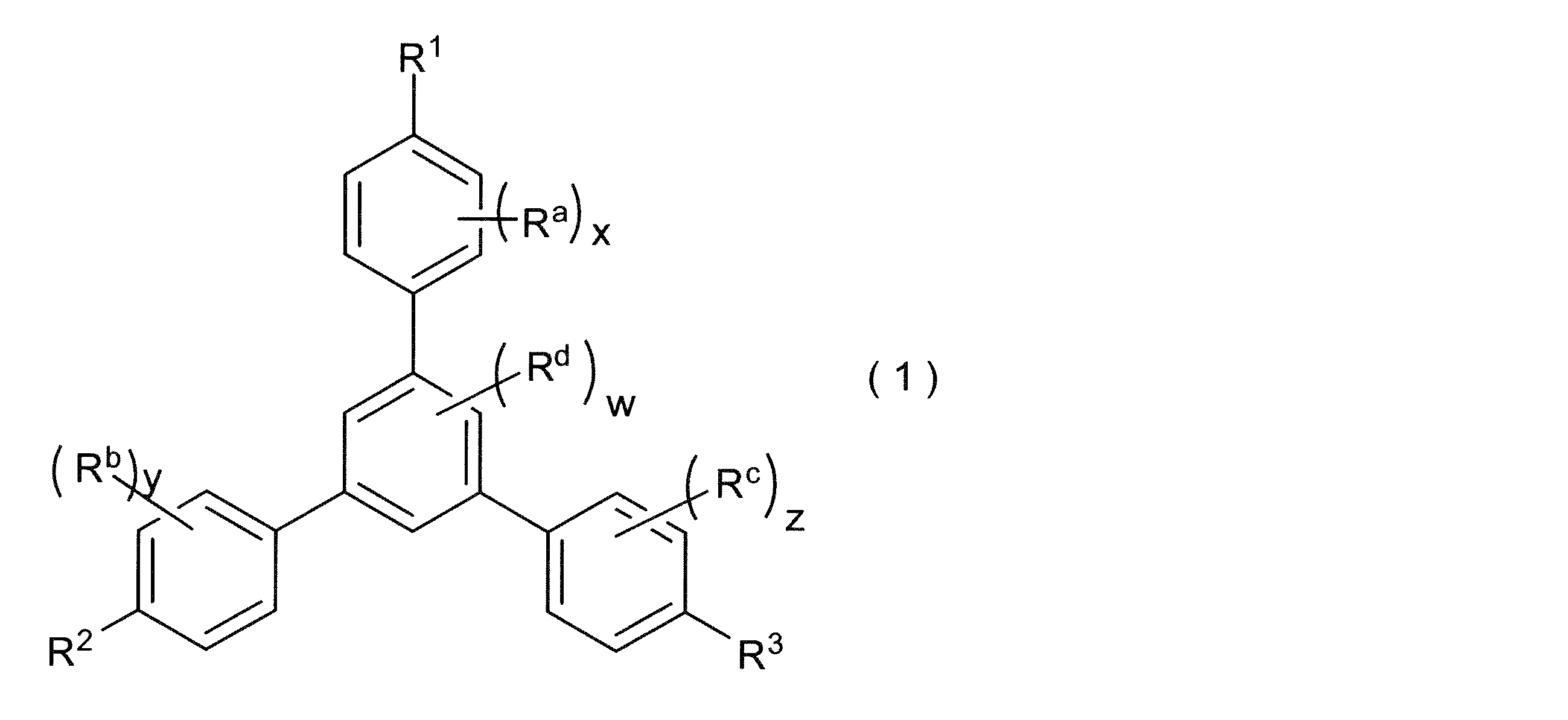
- a compound is a compound denoted by a following formula (1).
- R 1 , R 2 and R 3 are groups represented by the following formula (a).
- R 1 , R 2 and R 3 may be the same or different.
- R a , R b , R c, and R d each independently represent a halogen atom, a hydroxy group, an amino group, a sulfanyl group, or a monovalent organic group having 1 to 20 carbon atoms that does not contain an aromatic ring.
- x, y, and z are each independently an integer of 0 to 4.
- w is an integer of 0 to 3.
- the plurality of R a may be the same or different
- the plurality of R b may be the same or different
- the plurality of R c may be the same or different
- a plurality of R d may be the same or different.
- R A is a hydrogen atom, an aryl group, or an alkyl group substituted or unsubstituted with at least one of a hydroxy group and an aryl group.
- R B is a single bond or an arylene group. Part or all of the hydrogen atoms on the aromatic ring of the aryl group and arylene group are substituted with a halogen atom, a hydroxy group, an amino group, a sulfanyl group, or a monovalent organic group having 1 to 20 carbon atoms that does not contain an aromatic ring. It may be.
- Examples of the aryl group represented by R A include a phenyl group, a tolyl group, a xylyl group, a naphthyl group, and an anthryl group.
- the number of carbon atoms of the aryl group is preferably 6-20, and more preferably 6-10.
- a phenyl group and a naphthyl group are preferable, and a phenyl group is more preferable.
- Examples of the alkyl group represented by R A include a methyl group, an ethyl group, an n-propyl group, an i-propyl group, an n-butyl group, an i-butyl group, a sec-butyl group, a t-butyl group, Examples thereof include an n-pentyl group and an n-hexyl group.
- the number of carbon atoms of the alkyl group is preferably 1 to 10, and more preferably 1 to 6.
- the alkyl group is preferably an n-alkyl group, more preferably a methyl group, an ethyl group, an n-propyl group, or an n-butyl group from the viewpoint of improving the heat resistance of the resist underlayer film to be formed.
- Examples of the aryl group for substituting the alkyl group include the same groups as those exemplified as the aryl group for RA .
- Examples of the alkyl group substituted with the aryl group represented by R A include a benzyl group, a phenethyl group, a diphenylmethyl group, a diphenylethyl group, a dinaphthylmethyl group, and the like.
- Examples of the alkyl group substituted with a hydroxy group represented by R A include, for example, a hydroxymethyl group, a hydroxyethyl group, a 2-hydroxy-2-propyl group, a dihydroxyethyl group, and 1,3-dihydroxy-2-propyl. Groups and the like.
- Examples of the alkyl group substituted with the hydroxy group and aryl group represented by R A include a hydroxyphenylmethyl group, a hydroxydiphenylmethyl group, a hydroxydiphenylethyl group, a dihydroxydiphenylethyl group, and the like.
- a fluorine atom and a chlorine atom are preferable, and a fluorine atom is more preferable.
- Examples of the monovalent organic group having 1 to 20 carbon atoms that does not include an aromatic ring for substituting a hydrogen atom on the aromatic ring of the aryl group include, for example, a monovalent chain hydrocarbon group having 1 to 20 carbon atoms, carbon A group ( ⁇ ) containing a divalent heteroatom-containing group between carbon and carbon of the monovalent alicyclic hydrocarbon group of the number 3 to 20, the chain hydrocarbon group and the alicyclic hydrocarbon group, Examples include a chain hydrocarbon group, a group obtained by substituting a part or all of the hydrogen atoms of the alicyclic hydrocarbon group and the group ( ⁇ ) with a monovalent heteroatom-containing group having no aromatic ring. .
- Examples of the chain hydrocarbon group include: Alkyl groups such as methyl, ethyl, propyl and butyl groups; Examples thereof include alkenyl groups such as ethenyl group, propenyl group and butenyl group; alkynyl groups such as ethynyl group, propynyl group and butynyl group.
- Examples of the alicyclic hydrocarbon group include: Cycloalkyl groups such as cyclopropyl group, cyclobutyl group, cyclopentyl group, cyclohexyl group, cyclooctyl group, norbornyl group, adamantyl group; And cycloalkenyl groups such as cyclopropenyl group, cyclobutenyl group, cyclopentenyl group, cyclohexenyl group, cyclooctenyl group, norbornenyl group, and the like.
- divalent heteroatom-containing group examples include —O—, —NR ′′ — (R ′′ represents a chain hydrocarbon group having 1 to 10 carbon atoms or an alicyclic hydrocarbon group having 3 to 10 carbon atoms. ), -S-, carbonyl group, carbonyloxy group, carbonylamino group, sulfonamide group and the like.
- Examples of the monovalent heteroatom-containing group include a halogen atom, a hydroxy group, an amino group, a sulfanyl group, a cyano group, a nitro group, and an aminosulfonyl group.
- the group that replaces the hydrogen atom on the aromatic ring of the aryl group is preferably a hydroxy group, an amino group, or a monovalent organic group having 1 to 20 carbon atoms that does not contain an aromatic ring.
- Group, alkoxy group and cycloalkyloxy group are more preferred, and hydroxy group, amino group, hydroxymethyl group, methoxy group and ethoxy group are more preferred.
- R A is a C 6-20 carbon atom substituted with a hydrogen atom, an unsubstituted aryl group having 6-20 carbon atoms, a hydroxy group or an amino group.
- Preferred are an aryl group, an unsubstituted alkyl group having 1 to 10 carbon atoms, an alkyl group having 1 to 10 carbon atoms substituted with a hydroxy group, and an alkyl group having 1 to 10 carbon atoms substituted with a hydroxy group and an aryl group. More preferred are a phenyl group, a hydroxymethyl group, a 2-hydroxy-2-propyl group, a hydroxydiphenylmethyl group, and a phenyl group substituted with an amino group.
- Examples of the arylene group represented by R B include a phenylene group, a tolylene group, a xylylene group, a naphthylene group, and an anthrylene group.
- the number of carbon atoms of the arylene group is preferably 6 to 20, and more preferably 6 to 10.
- a phenylene group and a naphthylene group are preferable, and a phenylene group is more preferable.
- halogen atom for substituting the hydrogen atom on the aromatic ring of the arylene group and the monovalent organic group having 1 to 20 carbon atoms not containing the aromatic ring include, for example, a hydrogen atom on the aromatic ring of the aryl group in R A Groups similar to those exemplified as the halogen atom for substituting and the monovalent organic group.
- R B is preferably a single bond or an unsubstituted arylene group having 6 to 10 carbon atoms, more preferably a single bond or a phenylene group, from the viewpoint of improving the heat resistance of the resist underlayer film to be formed.
- Examples of the monovalent organic group having 1 to 20 carbon atoms which does not include a halogen atom and an aromatic ring represented by R a to R d in the above formula (1) include, for example, an aryl group and an arylene group in the above formula (a). Groups similar to those exemplified as the halogen atom for substituting and the monovalent organic group.
- R a to R d in the above formula (1) are preferably a halogen atom, a monovalent organic group having 1 to 20 carbon atoms that does not contain an aromatic ring, a halogen atom, an alkyl group having 1 to 10 carbon atoms, a carbon number A 1 to 10 hydroxyalkyl group is more preferable, and a fluorine atom, a methyl group, an ethyl group, and a hydroxymethyl group are more preferable.
- x, y, z and w are preferably integers of 0 to 2, more preferably 0 or 1, and even more preferably 0 from the viewpoint of improving the heat resistance of the resist underlayer film to be formed.
- the aromatic ring in the aryl group and arylene group of the above formula (a) preferably has no substituent from the viewpoint of improving the heat resistance of the resist underlayer film to be formed.
- R 1 , R 2 and R 3 in the above formula (1) may be the same or different, but from the viewpoint of improving the flatness of the resist underlayer film to be formed, and from the viewpoint of ease of synthesis of the [A] compound, It is preferable that they are the same.
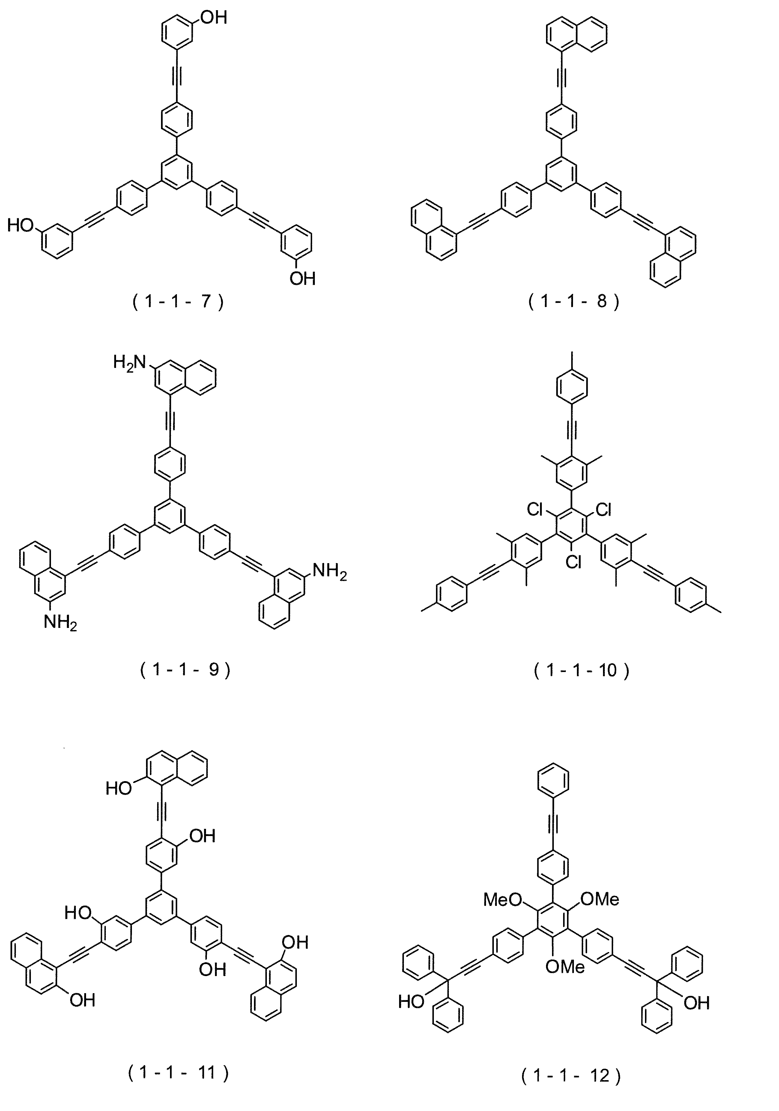
- Examples of the compound [A] include the compounds represented by the following formulas (1-1-1) to (1-1-12) (wherein R B is a single bond and R A is other than a hydrogen atom) "Compounds (I-1-1) to (I-1-12)”) and the like.
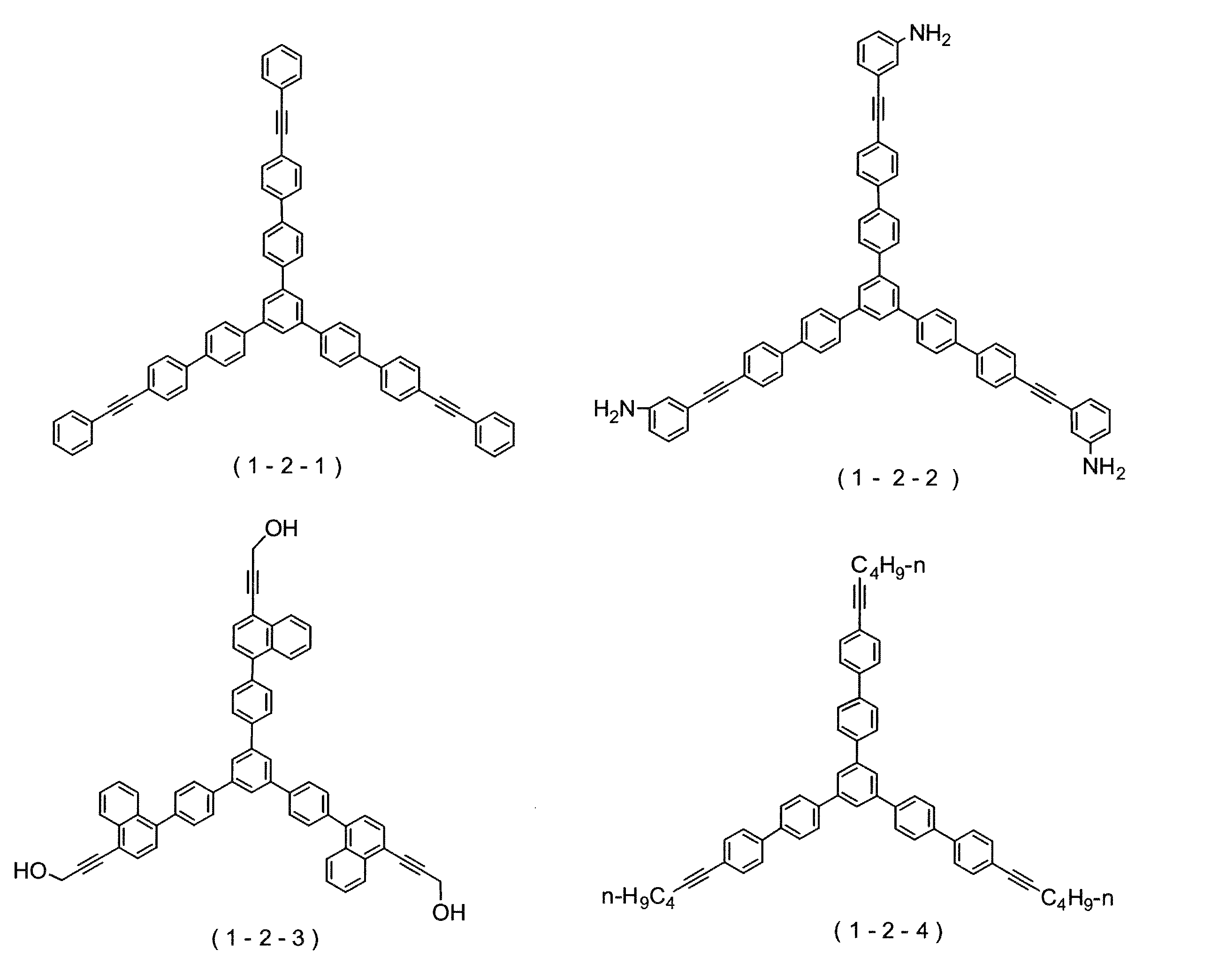
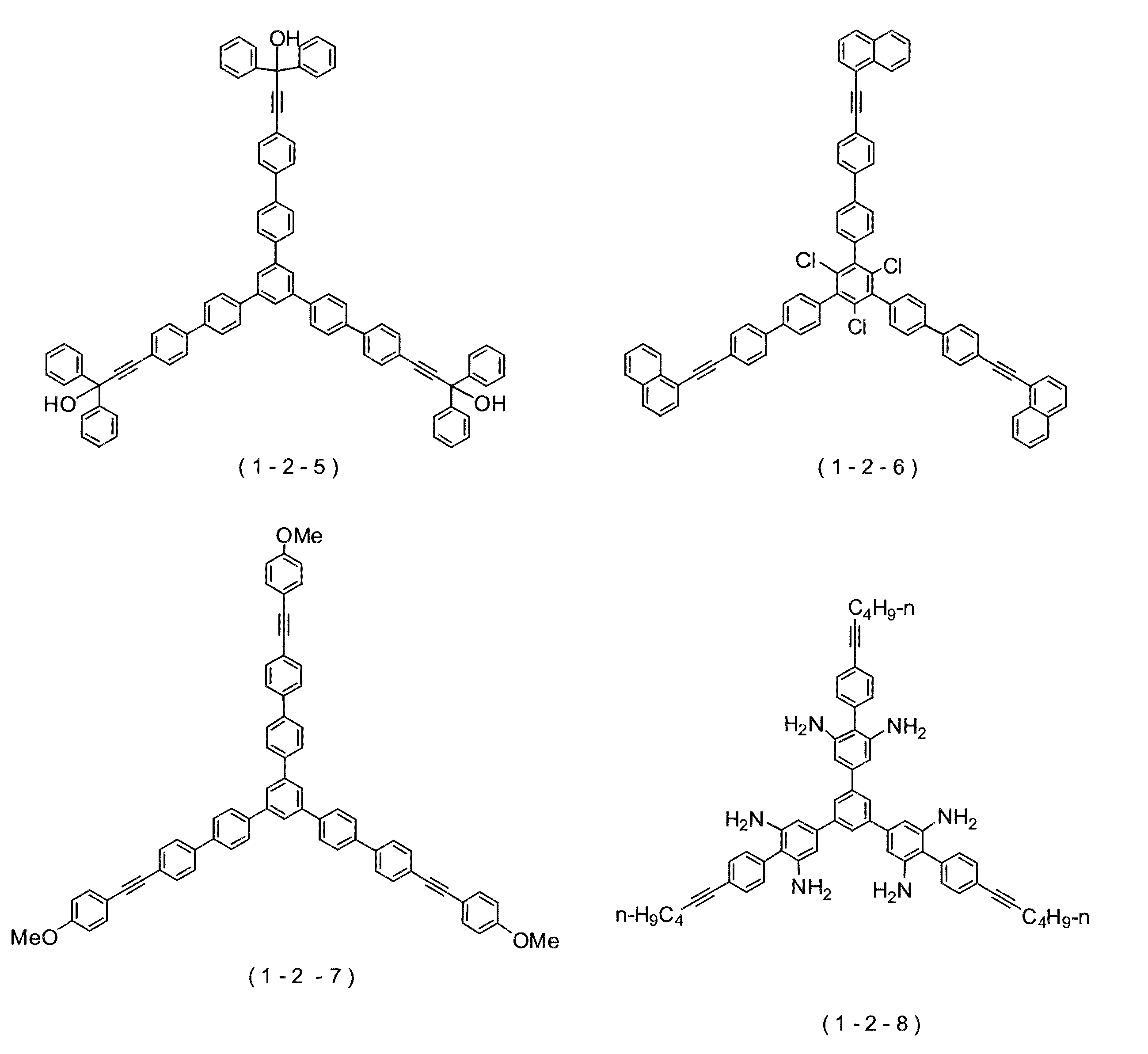
- Examples of the compound [A] include compounds represented by the following formulas (1-2-1) to (1-2-8) when R B is other than a single bond and R A is other than a hydrogen atom (hereinafter referred to as “A”). And “compounds (I-2-1) to (I-2-8)").
- R 1 , R 2 and R 3 are groups represented by the following formula (a ′).
- R 1 , R 2 and R 3 may be the same or different.
- R a ′ , R b ′ , R c ′, and R d ′ each independently represent a halogen atom, a hydroxy group, an amino group, a sulfanyl group, or a monovalent organic group having 1 to 20 carbon atoms that does not contain an aromatic ring. It is.
- x ′, y ′ and z ′ are each independently an integer of 0 to 4.
- w ′ is an integer of 0 to 3.
- the plurality of R a ′ may be the same or different
- the plurality of R b ′ may be the same or different
- the plurality of R c ′ may be the same or different
- the plurality of R d ′ may be the same or different.
- R A ′ is a hydrogen atom, an aryl group, or an unsubstituted or substituted alkyl group substituted with at least one of a hydroxy group and an aryl group.
- R B ′ is a single bond or an arylene group. Part or all of the hydrogen atoms on the aromatic ring of the aryl group and arylene group are substituted with a halogen atom, a hydroxy group, an amino group, a sulfanyl group, or a monovalent organic group having 1 to 20 carbon atoms that does not contain an aromatic ring. It may be. However, at least one of the three R A ′ in the above compound is a hydrogen atom.
- R a ′ to R d ′ and x ′ to w ′ in the above formula (1 ′) and R A ′ and R B ′ in the above formula (a ′) R a to R d in the above formula (1) and Examples thereof include the same groups as those exemplified as x to w and R A and R B in the above formula (a).
- RA ′ in the compound (I ′) two or more are preferably hydrogen atoms from the viewpoint of further improving the curability of the film-forming composition, and all three are hydrogen atoms. It is more preferable.
- Examples of the compound (I ′) include compounds represented by the following formulas (1-3-1) to (1-3-8) (hereinafter referred to as “compounds (I-3-1) to (I-3- 8) ”)) and the like.
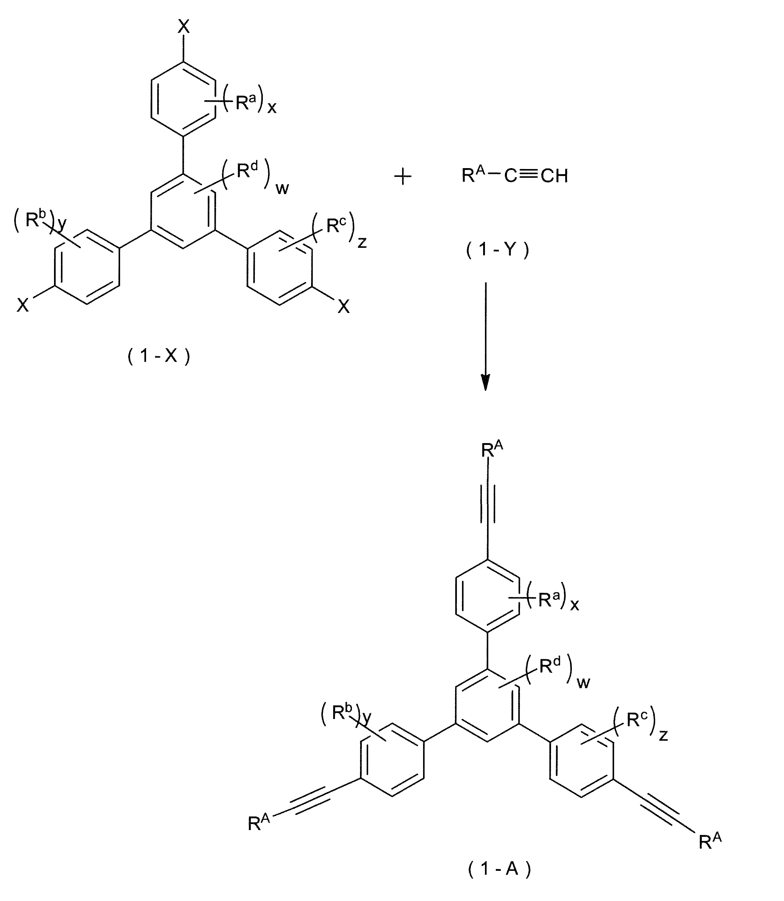
- the compound [A] is, for example, a compound in which R B of the group (a) is a single bond and R A is other than a hydrogen atom (a compound represented by the following formula (1-A)), according to the following reaction scheme: Can be synthesized.
- X is a halogen atom.
- R A is an aryl group or an alkyl group substituted or unsubstituted with at least one of a hydroxy group and an aryl group.
- a plurality of X may be the same or different.
- a plurality of RA may be the same or different.
- R a , R b , R c, and R d each independently represent a halogen atom, a hydroxy group, an amino group, a sulfanyl group, or a monovalent organic group having 1 to 20 carbon atoms that does not contain an aromatic ring.
- x, y, and z are each independently an integer of 0 to 4.
- w is an integer of 0 to 3.
- the plurality of R a may be the same or different
- the plurality of R b may be the same or different
- the plurality of R c may be the same or different
- a plurality of R d may be the same or different.
- a compound represented by the above formula (1-X) (1,3,5-tris (p-halophenyl) benzene) and an ethynyl compound represented by the above formula (1-Y) are mixed with dichlorobistriphenylphosphine palladium.
- a palladium catalyst such as (II)
- a copper (I) catalyst such as copper (I) iodide
- a base such as triethylamine
- the above X is preferably a chlorine atom, a bromine atom or an iodine atom, more preferably a bromine atom, from the viewpoint of improving the yield of the compound [A].
- R B of the group (a) is an arylene group and R A is other than a hydrogen atom is, for example, 1,3,5-tris (4′-halo) instead of the compound (1-X). It can be synthesized by using biphenyl-4-yl) benzene or the like.
- the compound [A] in which R A of the group (a) is a hydrogen atom is obtained by using a silylated acetylene compound such as trimethylsilylacetylene to obtain a reaction product with the compound (1-X) and the like.
- a silylated acetylene compound such as trimethylsilylacetylene
- the lower limit of the molecular weight of the [A] compound is preferably 400, more preferably 450, still more preferably 500, and particularly preferably 550, from the viewpoint of improving the heat resistance of the resist underlayer film to be formed.
- the upper limit of the molecular weight of the compound [A] is preferably 1,000, preferably 900, more preferably 800, and particularly preferably 700, from the viewpoint of improving the flatness of the resist underlayer film to be formed.
- the lower limit of the carbon content of the compound is preferably 50 atom%, more preferably 55 atom%, and still more preferably 60 atom%. Moreover, as a minimum of the carbon content rate of a [A] compound, 80 mass% is preferable, 85 mass% is more preferable, and 90 mass% is further more preferable. The higher the carbon content, the better. [A] By making the carbon content rate of a compound into the said range, the heat resistance of the resist underlayer film formed can further be improved.
- the content of the [A] compound in the film-forming composition is preferably 80% by mass or more, more preferably 90% by mass or more, and further preferably 95% by mass or more based on the total solid content.
- the solvent is not particularly limited as long as it is a solvent capable of dissolving or dispersing the [A] compound and optionally contained optional components.
- Examples of the solvent include alcohol solvents, ether solvents, ketone solvents, amide solvents, ester solvents, hydrocarbon solvents, and the like.
- an alcohol solvent for example, C1-C18 aliphatic monoalcohol solvents such as 4-methyl-2-pentanol, n-hexanol; An alicyclic monoalcohol solvent having 3 to 18 carbon atoms such as cyclohexanol; A polyhydric alcohol solvent having 2 to 18 carbon atoms such as 1,2-propylene glycol; Examples thereof include polyhydric alcohol partial ether solvents having 3 to 19 carbon atoms such as propylene glycol monomethyl ether.
- ether solvent for example, Dialkyl ether solvents such as diethyl ether, dipropyl ether, dibutyl ether; Cyclic ether solvents such as tetrahydrofuran and tetrahydropyran; And aromatic ring-containing ether solvents such as diphenyl ether and anisole.
- ketone solvents include acetone, methyl ethyl ketone, methyl-n-propyl ketone, methyl-n-butyl ketone, diethyl ketone, methyl-iso-butyl ketone, 2-heptanone, ethyl-n-butyl ketone, methyl-n-hexyl ketone, Linear ketone solvents such as di-iso-butyl ketone and trimethylnonanone; Cyclic ketone solvents such as cyclopentanone, cyclohexanone, cycloheptanone, cyclooctanone, methylcyclohexanone; Examples include 2,4-pentanedione, acetonylacetone, acetophenone, and the like.
- amide solvent examples include cyclic amide solvents such as N, N′-dimethylimidazolidinone and N-methylpyrrolidone; Examples thereof include chain amide solvents such as N-methylformamide, N, N-dimethylformamide, N, N-diethylformamide, acetamide, N-methylacetamide, N, N-dimethylacetamide, and N-methylpropionamide.
- cyclic amide solvents such as N, N′-dimethylimidazolidinone and N-methylpyrrolidone
- chain amide solvents such as N-methylformamide, N, N-dimethylformamide, N, N-diethylformamide, acetamide, N-methylacetamide, N, N-dimethylacetamide, and N-methylpropionamide.
- ester solvents include: Monocarboxylic acid ester solvents such as acetates such as n-butyl acetate; Polyhydric alcohol carboxylate solvents such as propylene glycol acetate; Polyhydric alcohol partial ether carboxylate solvents such as polyhydric alcohol partial alkyl ether acetates such as propylene glycol acetate monomethyl ether acetate; Polycarboxylic acid diester solvents such as diethyl oxalate; Lactone solvents such as ⁇ -butyrolactone and ⁇ -valerolactone; Examples include carbonate solvents such as diethyl carbonate, ethylene carbonate, and propylene carbonate.
- Monocarboxylic acid ester solvents such as acetates such as n-butyl acetate
- Polyhydric alcohol carboxylate solvents such as propylene glycol acetate
- Polyhydric alcohol partial ether carboxylate solvents such as polyhydric alcohol partial alkyl ether acetates such
- hydrocarbon solvent examples include linear or branched hydrocarbons having 5 to 10 carbon atoms, alicyclic hydrocarbons having 5 to 12 carbon atoms, aromatic hydrocarbons having 6 to 18 carbon atoms, and the like. It is done. Some or all of the hydrogen atoms on the ring of the alicyclic hydrocarbon and aromatic hydrocarbon may be substituted with a linear or branched alkyl group having 1 to 5 carbon atoms.
- the film-forming composition may contain one or more [B] solvents.
- the acid generator is a component that generates an acid upon exposure or heating.
- the film-forming composition can cause a crosslinking reaction to proceed between the [A] compounds at a relatively low temperature including normal temperature.
- photo acid generator examples include those described in paragraphs [0077] to [0081] of JP-A No. 2004-168748.
- the acid generator that generates an acid by heating is, for example, 2, 4 , 4,6-tetrabromocyclohexadienone, benzoin tosylate, 2-nitrobenzyl tosylate, alkylsulfonates and the like.
- thermal acid generators are preferable, onium salt acid generators are more preferable, iodonium salt acid generators are more preferable, diphenyliodonium trifluoromethanesulfonate, diphenyliodonium nonafluoro-n.
- the content of the acid generator is preferably 5,000 parts by mass or less, more preferably 0.1 parts by mass to 500 parts by mass, and 0.5 parts by mass with respect to 100 parts by mass of the compound [A]. Is more preferably from 100 parts by weight, and particularly preferably from 1 part by weight to 20 parts by weight. [C] By making content of an acid generator into the said range, the intensity
- the crosslinking agent is a compound having a crosslinkable group.
- the said film formation composition can perform the bridge
- crosslinking agent what has two or more crosslinkable groups is preferable.
- crosslinking agent examples include polynuclear phenols, alkoxymethylated melamine, alkoxymethylated glycoluril, diisocyanates, compounds represented by the following formula (d) (hereinafter referred to as “compound (d)”) And the like).
- Ar is an n-valent aromatic hydrocarbon group or an n-valent heteroaromatic group.
- Y is a carbonyl group or a sulfonyl group.
- Q is a monovalent heteroaromatic group or —OR 4 .
- R 4 is a monovalent organic group having 1 to 30 carbon atoms.
- n is an integer of 2 to 7.
- a plurality of Y may be the same or different.
- a plurality of Q may be the same or different.
- n-valent aromatic hydrocarbon group represented by Ar examples include n benzene, toluene, xylene, naphthalene, anthracene, indene, fluorenylidene biphenyl, and other n bonds bonded to the aromatic ring.
- examples include a group excluding a hydrogen atom.
- n-valent heteroaromatic group represented by Ar examples include heteroaromatic compounds such as furan, pyrrole, thiophene, phosphole, pyrazole, oxazole, isoxazole, thiazole, pyridine, pyrazine, pyrimidine, pyridazine, and triazine. From the above, groups excluding n hydrogen atoms bonded to the heteroaromatic ring, and the like can be mentioned.
- Y is preferably a carbonyl group.
- Examples of the monovalent heteroaromatic group represented by Q include a group obtained by adding (n-1) hydrogen atoms to those exemplified as the n-valent heteroaromatic group represented by Ar above Is mentioned.
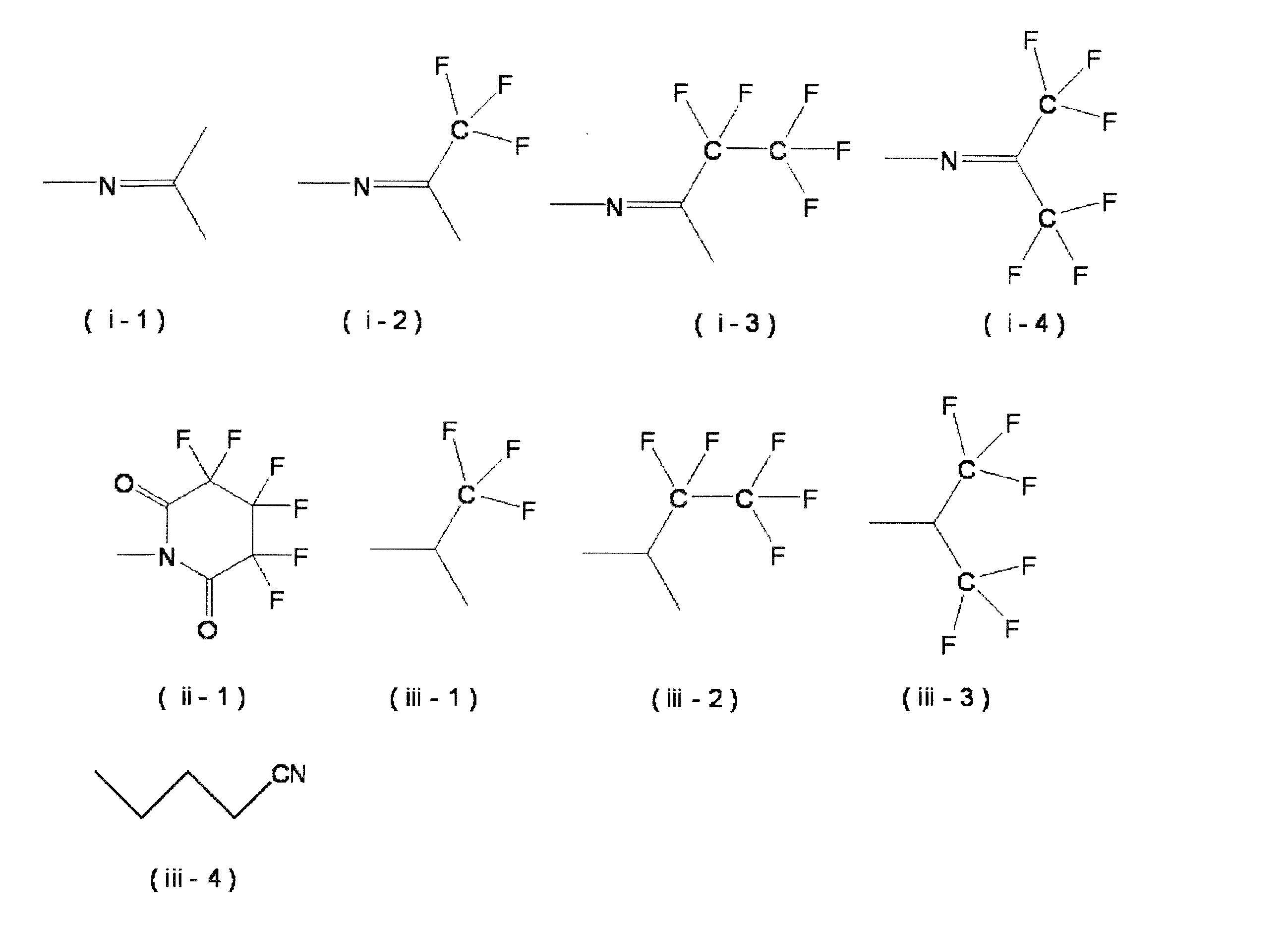
- Examples of the monovalent organic group having 1 to 30 carbon atoms represented by R 4 of —OR 4 in Q above include groups represented by the following formulas (i) to (iii) (hereinafter referred to as “group (i ) To (iii) ”) and the like.
- R 5 and R 6 are each independently a monovalent organic group having 1 to 20 carbon atoms, or these groups are combined with each other and configured with a carbon atom to which they are bonded. Represents a ring structure having 3 to 20 ring members.
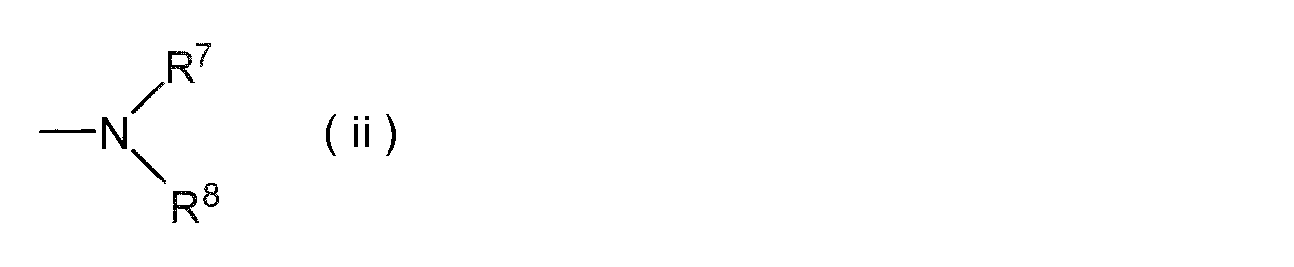
- R 7 and R 8 are each independently a monovalent organic group having 1 to 20 carbon atoms, or these groups are combined with each other and configured with a nitrogen atom to which they are bonded. Represents a ring structure having 3 to 20 ring members.
- R 9 is a C 1-20 monovalent organic group having an electron withdrawing group.
- Examples of the monovalent organic group having 1 to 20 carbon atoms represented by R 5 to R 8 include, for example, a monovalent hydrocarbon group having 1 to 20 carbon atoms, the hydrocarbon group and —CO—, —COO.
- a heteroatom-containing group in combination with at least one group selected from the group consisting of —, —O—, —NR′—, —CS—, —S—, —SO— and —SO 2 —, the hydrocarbon And a group in which part or all of the hydrogen atoms of the group and the heteroatom-containing group are substituted with a fluorine atom, a hydroxy group, a carboxy group, a cyano group, or the like.
- R ′ is a hydrogen atom or a monovalent hydrocarbon group having 1 to 20 carbon atoms.
- Examples of the monovalent hydrocarbon group having 1 to 20 carbon atoms include: A chain hydrocarbon group having 1 to 20 carbon atoms such as an alkyl group such as a methyl group, an ethyl group or a propyl group, an alkenyl group such as an ethenyl group or a propenyl group, an alkynyl group such as an ethynyl group or a propynyl group; An alicyclic hydrocarbon group having 3 to 20 carbon atoms such as a cycloalkyl group such as cyclopropyl group, cyclobutyl group, cyclopentyl group, norbornyl group, cyclopropenyl group, cyclobutenyl group, cyclopentenyl group, norbornyl group; Examples thereof include aryl groups such as phenyl group, tolyl group, xylyl group and naphthyl group, and aromatic hydrocarbon groups having 6 to 20 carbon atoms such as
- Examples of the ring structure having 3 to 20 ring members composed of R 5 and R 6 together with the carbon atom to which they are bonded include a cyclopropane structure, a cyclobutane structure, a cyclopentane structure, a cyclohexane structure, and the like.
- Examples of the ring structure having 3 to 20 ring members constituted by the nitrogen atom to which R 7 and R 8 are combined with each other and bonded to each other include, for example, an azacyclopropane structure, an azacyclobutane structure, an azacyclopentane structure, an azacyclohexane structure Etc.
- Examples of the monovalent organic group having 1 to 20 carbon atoms and having an electron withdrawing group represented by R 9 include, for example, 1 to 20 carbon atoms in which some or all of the hydrogen atoms are substituted with electron withdrawing groups. And monovalent hydrocarbon groups.
- As said electron withdrawing group halogen atoms, such as a fluorine atom and a chlorine atom, a nitro group, a cyano group etc. are mentioned, for example. Among these, a fluorine atom, a nitro group, and a cyano group are preferable.
- Examples of the group (i) include groups represented by the following formulas (i-1) to (i-4), and examples of the group (ii) include groups represented by the following formula (ii-1). However, examples of the group (iii) include groups represented by the following formulas (iii-1) to (iii-4).
- N is preferably an integer of 2 to 5, more preferably 2 or 3, and still more preferably 2.
- polynuclear phenols examples include dinuclear phenols such as 4,4′-biphenyldiol, 4,4′-methylene bisphenol, 4,4′-ethylidene bisphenol, and bisphenol A; 4,4 ′, 4 ′′- Methylidenetrisphenol, 4,4 ′-(1- (4- (1- (4-hydroxyphenyl) -1-methylethyl) phenyl) ethylidene) bisphenol, 4,4 ′-(1- (4- (1 Trinuclear phenols such as-(4-hydroxy-3,5-bis (methoxymethyl) phenyl) -1-methylethyl) phenyl) ethylidene) bis (2,6-bis (methoxymethyl) phenol); Examples include polyphenols.
- alkoxymethylated melamine examples include hexakis (methoxymethyl) melamine and hexakis (n-butoxymethyl) melamine.
- alkoxymethylated glycoluril examples include 1,3,4,6-tetrakis (methoxymethyl) glycoluril, 1,3,4,6-tetrakis (n-butoxymethyl) glycoluril and the like.
- diisocyanates examples include 2,3-tolylene diisocyanate, 2,4-tolylene diisocyanate, 3,4-tolylene diisocyanate, 3,5-tolylene diisocyanate, 4,4 ′ -Diphenylmethane diisocyanate, hexamethylene diisocyanate, 1,4-cyclohexane diisocyanate and the like.
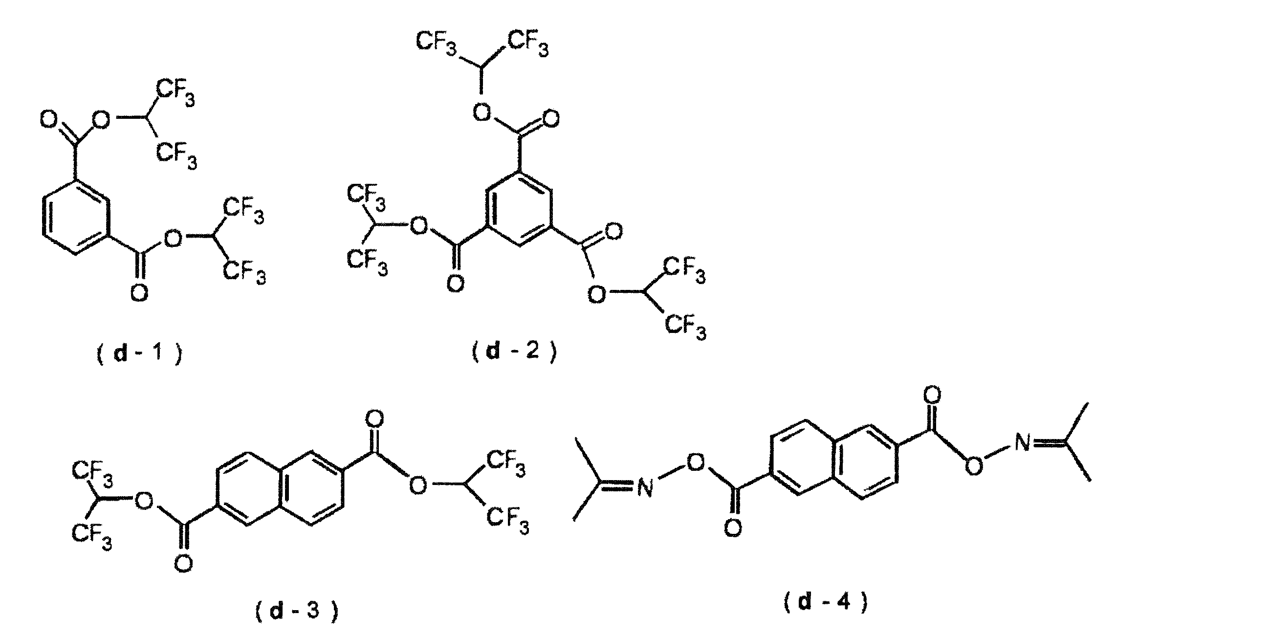
- Examples of the compound (d) include compounds represented by the following formulas (d-1) to (d-4).
- the polynuclear phenols, alkoxymethylated glycoluril and compound (d) obtained are preferred as the crosslinking agent, and 4,4 ′-(1- (4- (1- (4-hydroxy Phenyl) -1-methylethyl) phenyl) ethylidene) bisphenol, 1,3,4,6-tetrakis (methoxymethyl) glycoluril, a compound represented by the above formula (d-1) (1,3-di (1 1,1,3,3,3-hexafluoropropan-2-yloxycarbonyl) benzene).
- the said film formation composition can further improve the heat resistance and intensity
- crosslinking agents examples include: “Epicoat 812", 815, 826, 828, 834, 836, 836, 871, 1001, 1004, 1007, 1009, 1031 (above, made by Yuka Shell Epoxy), “Araldite 6600 “, 6700, 6800, 502, 6071, 6084, 6097, 6097, 6099 (above, manufactured by Ciba Geigy),” DER331 “, 332, 333, 661, 644, 667 ( Epoxy crosslinking agents such as Dow Chemical Co., Ltd.) "Cymel 300", 301, 303, 350, 370, 771, 325, 327, 703, 712, 701, 272, 202, “My Coat 506", 508 ( As described above, melamine crosslinking agents such as Mitsui Cyanamid Co., Ltd .; Benzoguanamine-based cross-linking agents such as “Cymel 1123”, 1123-10, 1128, “My Coat 506", 508 ( As
- the content of the crosslinking agent is preferably 1,000 parts by mass or less, more preferably 0.1 parts by mass to 500 parts by mass, and more preferably 1 part by mass to 100 parts by mass with respect to 100 parts by mass of the compound [A]. Part is more preferable, and 2 parts by weight to 50 parts by weight is particularly preferable. [D] By making content of a crosslinking agent into the said range, the heat resistance and intensity
- the film-forming composition includes, for example, a binder resin, an accelerator, a surfactant, a radiation absorber, a storage stabilizer, an antifoaming agent, Examples thereof include an adhesion aid.
- the said film formation composition can use the said other arbitrary component 1 type (s) or 2 or more types, respectively.
- the resist underlayer film to be formed improves resistance to an organic solvent contained in the composition that forms a resist film, an intermediate layer, or the like formed on the upper surface. be able to.
- the binder resin is not particularly limited as long as it is a polymer compound, but at least one selected from the group consisting of novolak resins, resol resins, styrene resins, acenaphthylene resins, and polyarylene resins is preferable.
- the resin By using the resin as the binder resin, the refractive index and extinction coefficient of the resist underlayer film can be controlled to more appropriate values. As a result, the rectangularity of the cross-sectional shape of the resist pattern formed is improved.
- novolak resin examples include phenols such as phenol, cresol, xylenol, resorcinol, bisphenol A, p-tert-butylphenol, p-octylphenol, ⁇ -naphthol, ⁇ -naphthol, 1,5-dihydroxynaphthalene, 2 And a resin obtained by reacting one or more phenolic compounds selected from the group consisting of naphthols such as 1,7-dihydroxynaphthalene with aldehydes or divinyl compounds using an acidic catalyst or the like. .
- phenols such as phenol, cresol, xylenol, resorcinol, bisphenol A, p-tert-butylphenol, p-octylphenol, ⁇ -naphthol, ⁇ -naphthol, 1,5-dihydroxynaphthalene, 2
- aldehydes examples include aldehydes such as formaldehyde; aldehyde sources such as paraformaldehyde and trioxane.
- divinyl compounds include divinylbenzene, dicyclopentadiene, tetrahydroindene, 4-vinylcyclohexene, 5-vinylnoborn-2-ene, ⁇ -pinene, ⁇ -pinene, limonene, 5-vinylnorbornadiene, and the like.
- Examples of the resol-based resin include resins obtained by reacting the phenolic compound with the aldehydes using an alkaline catalyst.
- styrenic resin examples include polystyrene; styrene copolymers such as styrene- ⁇ -methylstyrene copolymer and styrene-butadiene copolymer.
- the acenaphthylene-based resin examples include resins obtained by polymerizing a compound having an acenaphthylene skeleton in an appropriate polymerization form such as bulk polymerization or solution polymerization by radical polymerization, anionic polymerization, cationic polymerization, or the like.
- the acenaphthylene-based resin reacts with a polymer of a compound having an acenaphthylene skeleton under an acidic condition. It can also be obtained.
- polyarylene-based resin examples include polyarylene ether, polyarylene sulfide, polyarylene ether sulfone, polyarylene ether ketone, and the like.
- the binder resin preferably has a naphthalene ring.
- the refractive index and extinction coefficient of the resist underlayer film can be controlled to more appropriate values, and as a result, the rectangular shape of the cross-sectional shape of the resist pattern formed is further improved.
- the binder resin preferably has a group containing a carbon-carbon triple bond.
- the film-forming composition can improve the etching resistance and the bending resistance of the resist underlayer film to be formed because the binder resin contains the above group. Examples of the group containing a carbon-carbon triple bond include an ethynyl group and a propargyl group.
- the binder resin may contain a crosslinkable group.
- crosslinking between binder resins or between binder resin and [A] compound can be raised.
- the binder resin does not substantially contain a crosslinkable group, film shrinkage during the formation of the resist underlayer film can be suppressed, and as a result, the flatness of the formed resist underlayer film can be further improved. Can do.
- the weight average molecular weight (Mw) of the binder resin is preferably from 2,000 to 8,000, and more preferably from 3,000 to 7,000. By making Mw of binder resin into the said range, the solvent tolerance of the resist underlayer film formed from the said film formation composition can be improved more.
- the ratio (Mw / Mn) of the weight average molecular weight to the number average molecular weight (Mn) of the binder resin is preferably 1 to 5, more preferably 1 to 3, and further preferably 1 to 2.5.
- content of the said binder resin 5 mass parts or more and 1,000 mass parts or less are preferable with respect to 100 mass parts of [A] compounds, 10 mass parts or more and 700 mass parts or less are more preferable, 30 mass parts or more and 400 mass parts or less. More preferred is less than or equal to parts by weight.
- [E] By making content of resin into the said range, the solvent tolerance of the resist underlayer film formed from the said film formation composition can be improved more.
- the accelerator is a one-electron oxidizer for sufficiently causing a dehydrogenation reaction necessary for oxidative crosslinking.
- One-electron oxidant means an oxidant that itself undergoes one-electron transfer.
- cerium (IV) ammonium nitrate cerium ion (IV) obtains one electron and changes to cerium ion (III).
- radical oxidizing agents such as halogen obtain one electron and convert it to an anion.
- the phenomenon of oxidizing the oxide by taking one electron from the oxide (substrate, catalyst, etc.) is called one-electron oxidation, and the component that receives one electron at this time is called one-electron oxidizing agent.
- Examples of the one-electron oxidizing agent include (a) metal compounds, (b) peroxides, (c) diazo compounds, (d) halogens or halogen acids.
- the metal compound (a) examples include metal compounds containing cerium, lead, silver, manganese, osmium, ruthenium, vanadium, thallium, copper, iron, bismuth, and nickel.
- cerium salts such as cerium (IV) ammonium nitrate (CAN; ammonium hexanitratocerium (IV)), cerium (IV) acetate, cerium (IV) nitrate, cerium (IV) sulfate ( For example, tetravalent cerium salt), (a2) lead tetraacetate, lead oxide such as lead (IV) oxide (eg, tetravalent lead compound), (a3) silver (I) oxide, silver (II) oxide, Silver carbonate (Fetizon reagent), silver compounds such as silver nitrate, (a4) manganese compounds such as permanganate, activated manganese dioxide, manganese (III) salts, (a5) osmium compounds such as os
- Examples of the (b) peroxide include peracids such as peracetic acid and m-chloroperbenzoic acid; hydroxyperoxides such as hydrogen peroxide and alkylhydroxyperoxides such as t-butyl hydroperoxide; diacyl peroxide , Peracid ester, peracid ketal, peroxydicarbonate, dialkyl peroxide, peracid ketone and the like.
- Examples of the (c) diazo compound include 2,2'-azobisisobutyronitrile.
- halogen or halogen acid examples include halogen selected from chlorine, bromine and iodine, perhalogen acid, halogen acid, hypohalous acid, hypohalous acid and salts thereof.
- halogen in the halogen acid examples include chlorine, bromine and iodine.
- Specific examples of the halogen acid or a salt thereof include sodium perchlorate and sodium bromate.
- (b) peroxides and (c) diazo compounds are preferable, and m-chloroperbenzoic acid, t-butyl hydroperoxide, and 2,2′-azobisisobutyronitrile are preferable. More preferred. When these are used, there is little possibility that metal residues or the like adhere to the substrate.
- the content of the accelerator is preferably 1000 parts by weight or less, more preferably 0.01 parts by weight to 500 parts by weight, and more preferably 0.1 parts by weight to 100 parts by weight with respect to 100 parts by weight of the [A] compound. Further preferred.
- the surfactant is a component having an action of improving the coating property, striation, wettability, developability and the like of the film-forming composition.
- content of the said surfactant 15 mass parts or less are preferable with respect to 100 mass parts of [A] compounds, and 10 mass parts or less are more preferable.
- Surfactant may use 1 type (s) or 2 or more types.
- the film-forming composition can be prepared, for example, by mixing the [A] compound, the [B] solvent, and optional components contained as necessary at a predetermined ratio.
- the film-forming composition is preferably filtered after mixing, for example, with a filter of about 0.1 ⁇ m.
- the solid content concentration of the film-forming composition is preferably 0.1% by mass to 50% by mass, more preferably 0.5% by mass to 30% by mass, and further preferably 1% by mass to 20% by mass.
- the concentration of the compound [A] in the film-forming composition is preferably 0.1% by mass to 30% by mass, more preferably 0.5% by mass to 20% by mass, and further preferably 1% by mass to 15% by mass. preferable.
- the film-forming composition preferably has a viscosity of 1 cps or more and 5 cps or less, more preferably 1 cps or more and 3 cps or less when the solid content concentration is 20% by mass.
- the viscosity value within the above range, the embedding property is improved, and the flatness of the resist underlayer film to be formed is improved.
- the method for forming the resist underlayer film is as follows: A step of forming a coating film on the upper surface side of the substrate (hereinafter also referred to as “coating step”), and a step of firing the coating layer (hereinafter also referred to as “firing step”). Is provided.
- the coating film is formed from the film-forming composition.
- the method for forming the resist underlayer film since the film forming composition described above is used, a resist underlayer film having high heat resistance and high flatness can be formed.
- the method for forming the resist underlayer film can be suitably used for a substrate having a step or a substrate having a plurality of types of trenches, and can form a resist underlayer film having excellent flatness.
- each step will be described.
- the substrate examples include a silicon wafer and a wafer coated with aluminum.
- a substrate having a step, a substrate having a plurality of types of trenches, and the like can be suitably used, and a resist underlayer film having excellent flatness can be formed.
- the substrate having the plurality of types of trenches for example, substrates having different aspect ratios can be preferably used. Also for this aspect ratio, a mixture of various values can be used.
- the ratio of the maximum value to the minimum value in the aspect ratio is preferably 3 or more, more preferably 5 or more, 10 or more is more preferable, and 15 or more is particularly preferable.
- the method for applying the film-forming composition to the substrate is not particularly limited, and can be carried out by an appropriate method such as spin coating, cast coating, roll coating, or the like.
- the film thickness of the coating film formed is preferably 100 nm to 5 ⁇ m, more preferably 200 nm to 3 ⁇ m.
- the coating film formed in the coating film forming step is baked.
- the method for firing the coating film include a heating method.
- the heating temperature is preferably 100 ° C. to 400 ° C., more preferably 200 ° C. to 390 ° C., and further preferably 300 ° C. to 370 ° C.
- the heating time is preferably 5 seconds to 60 minutes, more preferably 10 seconds to 10 minutes, and even more preferably 30 seconds to 3 minutes.
- the atmosphere in this heating include air, inert gas such as nitrogen gas, and argon gas.
- the film thickness of the resist underlayer film to be formed is preferably 10 nm to 5 ⁇ m, more preferably 30 nm to 500 ⁇ m.
- the pattern forming method is: A step of forming a resist pattern on the upper surface side of the resist underlayer film (hereinafter also referred to as “resist pattern forming step”), and a step of sequentially etching the resist underlayer film and the substrate using the resist pattern as a mask (hereinafter referred to as “etching”). Also called “process”) Is provided.
- the resist underlayer film is formed by a method for forming the resist underlayer film.
- the pattern forming method is In the resist pattern forming step, an intermediate layer is formed on the upper surface side of the resist underlayer film, a resist pattern is formed on the upper surface side of the intermediate layer, In the etching step, it is preferable to further etch the intermediate layer.
- the resist underlayer film having high heat resistance and high flatness formed from the film forming composition described above is used, a good pattern can be formed.
- each step will be described.
- resist pattern formation process In this step, a resist pattern is formed on the upper surface side of the resist underlayer film.
- An intermediate layer may be formed on the upper surface side of the resist underlayer film, and a resist pattern may be formed on the upper surface side of the intermediate layer.
- the above intermediate layer is a layer having these functions in order to supplement the functions of the resist underlayer film and / or the resist film in providing a resist pattern or the like, or to provide the functions that they do not have.
- the antireflection film is formed as an intermediate layer, the antireflection function of the resist underlayer film can be supplemented.
- the intermediate layer can be formed of an organic compound or an inorganic oxide.
- the organic compound include commercially available materials such as “DUV-42”, “DUV-44”, “ARC-28”, and “ARC-29” manufactured by Brewer Science, and “AR-3” manufactured by Rohm and Haas. And commercially available materials such as “AR-19”.
- the inorganic oxide for example, commercially available materials such as “NFC SOG” series manufactured by JSR, polysiloxane, titanium oxide, alumina oxide, tungsten oxide and the like formed by a CVD method can be used.
- the method for forming the intermediate layer is not particularly limited, and examples thereof include a coating method and a CVD method. Among these, a coating method is preferable. When the coating method is used, the intermediate layer can be formed continuously after forming the resist underlayer film.
- the film thickness of the intermediate layer is not particularly limited, and is appropriately selected according to the function required for the intermediate layer, but is preferably 10 nm to 3 ⁇ m, more preferably 20 nm to 0.3 ⁇ m.
- Examples of a method for forming a resist pattern on the upper surface side of the resist underlayer film or intermediate layer include a method using photolithography. This method will be specifically described below.
- the method using photolithography is, for example, a step of forming a resist film on the upper surface side of the resist underlayer film using a resist composition (hereinafter also referred to as “resist film forming step”), A step of exposing the resist film (hereinafter also referred to as “exposure step”), and a step of developing the exposed resist film (hereinafter also referred to as “development step”).
- resist film forming step a step of forming a resist film on the upper surface side of the resist underlayer film using a resist composition
- exposure step A step of exposing the resist film
- development step a step of developing the exposed resist film
- a resist composition is used to form a resist film on the upper surface side of the resist underlayer film. Specifically, after applying the resist composition so that the obtained resist film has a predetermined thickness, the solvent in the coating film is volatilized by pre-baking to form the resist film.
- the resist composition examples include a positive or negative chemically amplified resist composition containing a photoacid generator, a positive resist composition comprising an alkali-soluble resin and a quinonediazide-based photosensitizer, and an alkali-soluble resin and a crosslinking agent. And negative resist compositions composed of an agent.
- the solid content concentration of the resist composition is preferably 5 to 50% by mass.
- the resist composition is preferably prepared by filtering with a filter having a pore size of about 0.2 ⁇ m. In this step, a commercially available resist composition can be used as it is.
- the coating method of the resist composition is not particularly limited, and can be performed by an appropriate method such as spin coating, cast coating, roll coating, or the like.
- the pre-baking temperature is appropriately selected according to the type of resist composition used, etc., but is preferably 30 ° C. to 200 ° C., more preferably 50 ° C. to 150 ° C.
- the resist film formed in the resist film forming step is exposed. This exposure is performed, for example, via a predetermined mask pattern and, if necessary, an immersion liquid.
- the exposure light depending on the type of photoacid generator used in the resist composition, for example, electromagnetic waves such as visible light, ultraviolet light, far ultraviolet light, X-rays, ⁇ -rays; electron beams, molecular beams, ion beams, Although appropriately selected from particle beams such as ⁇ rays, far ultraviolet rays are preferable, and KrF excimer laser light (248 nm), ArF excimer laser light (193 nm), F 2 excimer laser light (wavelength 157 nm), Kr 2 excimer laser Light (wavelength 147 nm), ArKr excimer laser light (wavelength 134 nm), and extreme ultraviolet light (wavelength 13 nm, etc.) are more preferred, and ArF excimer laser light is more preferred.
- post-baking can be performed in order to improve the resolution, pattern profile, developability, etc. of the resist pattern to be formed.
- the post-baking temperature is appropriately adjusted according to the type of resist composition used, but is preferably 50 ° C. to 200 ° C., more preferably 70 ° C. to 150 ° C.
- the developer used for the development is appropriately selected according to the type of resist composition used.
- alkali development specifically, for example, sodium hydroxide, potassium hydroxide, sodium carbonate, sodium silicate, sodium metasilicate, ammonia, ethylamine, n-propylamine, diethylamine, di-n-propylamine, triethylamine, Methyldiethylamine, dimethylethanolamine, triethanolamine, tetramethylammonium hydroxide, tetraethylammonium hydroxide, pyrrole, piperidine, choline, 1,8-diazabicyclo [5.4.0] -7-undecene, 1,5-diazabicyclo Examples include alkaline aqueous solutions such as [4.3.0] -5-nonene. When the intermediate layer is formed by performing the intermediate layer forming step, the influence of these alkaline aqueous solutions on the resist underlayer film can be suppressed.
- a water-soluble organic solvent for example, an alcohol such as methanol or ethanol, or a surfactant can be added.
- a developer containing an organic solvent can be used as the developer.
- the organic solvent include esters, ketones, ethers, alcohols, amides, hydrocarbons and the like. Organic solvent development has little effect on the resist underlayer film.
- a method using a nanoimprint method, a method using a self-organizing composition, or the like can also be used as a method for performing the resist pattern forming step.
- the etching method may be dry etching or wet etching.
- the dry etching can be performed using a known dry etching apparatus.
- the source gas during dry etching depends on the elemental composition of the object to be etched, but includes oxygen atoms such as O 2 , CO, and CO 2 , inert gases such as He, N 2 , and Ar, Cl 2 , chlorine gas such as BCl 3 , fluorine gas such as CHF 3 and CF 4 , gas of H 2 and NH 3 , etc. can be used. In addition, these gases can also be mixed and used.
- C-1 Bis (t-butylphenyl) iodonium nonafluoro n-butanesulfonate (compound represented by the following formula (C-1))
- D-1 “Nikarak N-2702” (compound represented by the following formula (D-1)) manufactured by Sanwa Chemical Co., Ltd.
- D-2 4,4 ′-(1- (4- (1- (4-hydroxy-3,5-bis (methoxymethyl) phenyl) -1-methylethyl) phenyl) ethylidene) bis (2,6- Bis (methoxymethyl) phenol (compound represented by the following formula (D-2))
- D-3 1,3-di (1,1,1,3,3,3-hexafluoropropan-2-yloxycarbonyl) benzene (compound represented by the following formula (D-3))
- Example 1 [A] 10 parts by mass of (A-1) as a compound and 100 parts by mass of (B-1) as a [B] solvent were mixed to obtain a solution. The solution was filtered through a membrane filter having a pore size of 0.1 ⁇ m to prepare a film-forming composition (J-1).
- Example 1 Film-forming compositions (J-2) to (J-9) and (CJ-1) were prepared in the same manner as in Example 1 except that the components having the types and contents shown in Table 1 were used. did. In Table 1, “-” indicates that the corresponding component was not used.
- Example 10 to 13 Film-forming compositions (J-10) to (J-13) were prepared in the same manner as in Example 1 except that the components having the types and contents shown in Table 2 were used. In Table 2, “-” indicates that the corresponding component was not used.
- a resist underlayer film having a thickness of 200 nm having a thickness of 200 nm.
- the shape of the resist underlayer film was observed with a scanning electron microscope (S-4800, manufactured by Hitachi High-Tech), and the difference between the maximum value and the minimum value ( ⁇ FT) of the resist underlayer film thickness on the trench or space was measured. .
- the flatness was evaluated as “A” (good) when the ⁇ FT was less than 20 nm, and “B” (bad) when the ⁇ FT was 20 nm or more.
- the resist underlayer film formed from the film-forming composition of the example satisfies the general characteristics of the refractive index, the absorption coefficient, and the etching resistance, and is used for the film formation of the comparative example. Compared to a resist underlayer film formed from the composition, it has high heat resistance and high flatness.
- the film forming composition and resist underlayer film forming method of the present invention it is possible to form a resist underlayer film that satisfies general characteristics such as optical characteristics and etching resistance and has high heat resistance and high flatness.
- the resist underlayer film of the present invention satisfies general characteristics such as optical characteristics and etching resistance and has high heat resistance and high flatness.
- the pattern forming method of the present invention since the resist underlayer film having high heat resistance and high flatness is used, a good pattern can be formed.
- the compound of the present invention can be particularly preferably used as a component of the film-forming composition. Therefore, they can be suitably used for pattern formation using a multilayer resist process in semiconductor device manufacturing where the pattern is further miniaturized.
- the film forming composition of the present invention can be suitably used for the aerospace industry requiring high heat resistance.
Landscapes
- Chemical & Material Sciences (AREA)
- Organic Chemistry (AREA)
- Physics & Mathematics (AREA)
- General Physics & Mathematics (AREA)
- Engineering & Computer Science (AREA)
- Architecture (AREA)
- Structural Engineering (AREA)
- Medicinal Chemistry (AREA)
- Chemical Kinetics & Catalysis (AREA)
- Polymers & Plastics (AREA)
- Health & Medical Sciences (AREA)
- Materials For Photolithography (AREA)
- Photosensitive Polymer And Photoresist Processing (AREA)
- Exposure And Positioning Against Photoresist Photosensitive Materials (AREA)
- Organic Low-Molecular-Weight Compounds And Preparation Thereof (AREA)
- Addition Polymer Or Copolymer, Post-Treatments, Or Chemical Modifications (AREA)
- Exposure Of Semiconductors, Excluding Electron Or Ion Beam Exposure (AREA)
Abstract
Description
高い平坦性を有することが要求される。このように、上記レジスト下層膜には、種々の特性が要求されるが、上記従来のレジスト下層膜形成用組成物では、これらの要求を満足させることはできていない。

(式(1)中、R1、R2及びR3は、下記式(a)で表される基である。R1、R2及びR3は、同一でも異なっていてもよい。Ra、Rb、Rc及びRdは、それぞれ独立して、ハロゲン原子、ヒドロキシ基、アミノ基若しくはスルファニル基又は芳香環を含まない炭素数1~20の1価の有機基である。x、y及びzは、それぞれ独立して、0~4の整数である。wは、0~3の整数である。Ra~Rdがそれぞれ複数の場合、複数のRaは同一でも異なっていてもよく、複数のRbは同一でも異なっていてもよく、複数のRcは同一でも異なっていてもよく、複数のRdは同一でも異なっていてもよい。)

(式(a)中、RAは、水素原子、アリール基、又はヒドロキシ基とアリール基との少なくともいずれかで置換された若しくは非置換のアルキル基である。RBは、単結合又はアリーレン基である。上記アリール基及びアリーレン基の芳香環上の水素原子の一部又は全部はハロゲン原子、ヒドロキシ基、アミノ基若しくはスルファニル基又は芳香環を含まない炭素数1~20の1価の有機基で置換されていてもよい。)
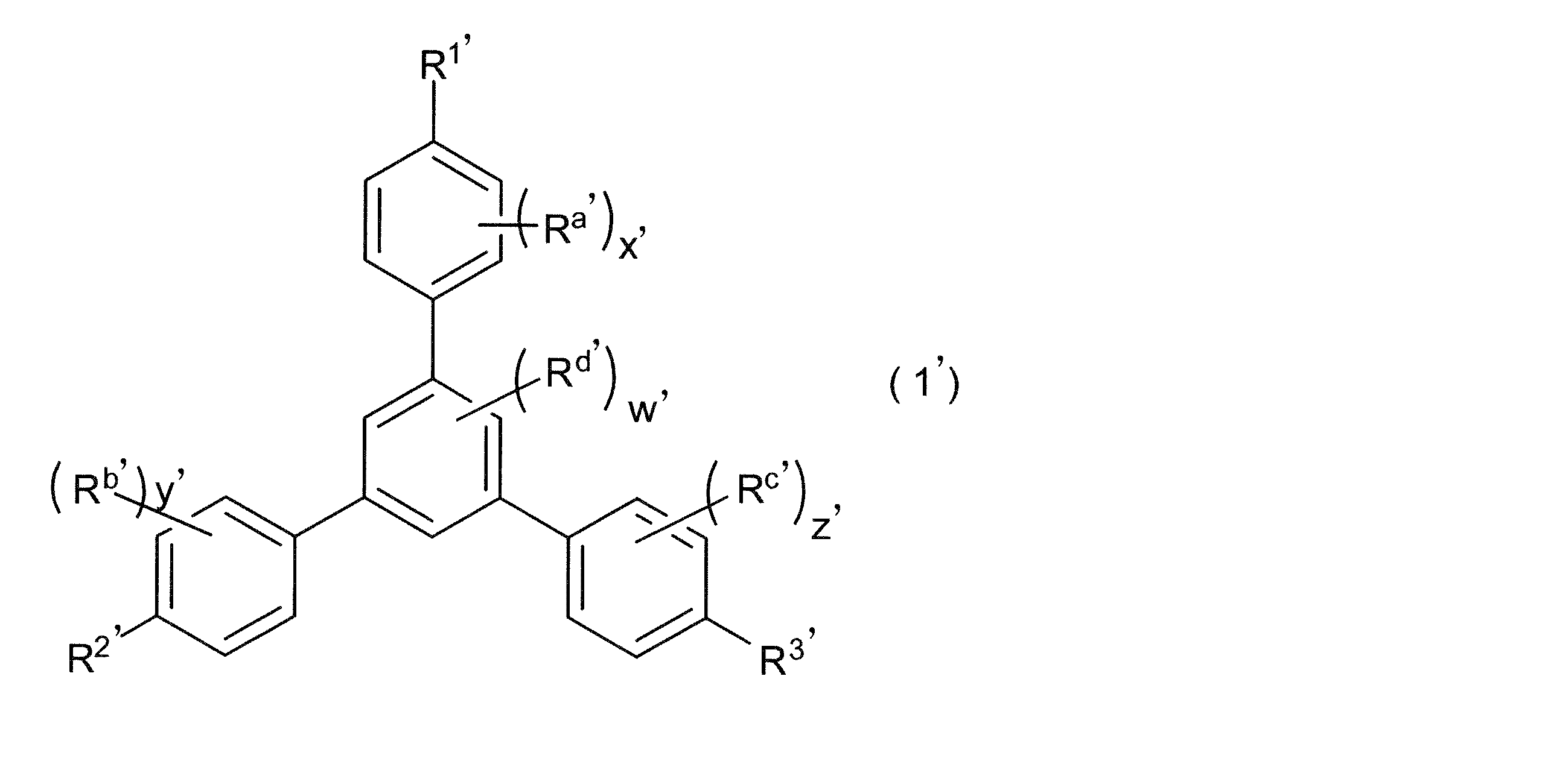
(式(1’)中、R1、R2及びR3は、下記式(a’)で表される基である。R1、R2及びR3は、同一でも異なっていてもよい。Ra’、Rb’、Rc’及びRd’は、それぞれ独立して、ハロゲン原子、ヒドロキシ基、アミノ基若しくはスルファニル基又は芳香環を含まない炭素数1~20の1価の有機基である。x’、y’及びz’は、それぞれ独立して、0~4の整数である。w’は、0~3の整数である。Ra’~Rd’がそれぞれ複数の場合、複数のRa’は同一でも異なっていてもよく、複数のRb’は同一でも異なっていてもよく、複数のRc’は同一でも異なっていてもよく、複数のRd’は同一でも異なっていてもよい。)

(式(a’)中、RA’は、水素原子、アリール基、又はヒドロキシ基とアリール基との少なくともいずれかで置換された若しくは非置換のアルキル基である。RB’は、単結合又はアリーレン基である。上記アリール基及びアリーレン基の芳香環上の水素原子の一部又は全部はハロゲン原子、ヒドロキシ基、アミノ基若しくはスルファニル基又は芳香環を含まない炭素数1~20の1価の有機基で置換されていてもよい。但し、上記化合物における3つのRA’のうちの少なくとも1つは水素原子である。)
当該膜形成用組成物は、[A]化合物及び[B]溶媒を含有する。当該膜形成用組成物は、好適成分として、酸発生剤(以下、「[C]酸発生剤」ともいう)、架橋剤(以下、「[D]架橋剤」ともいう)を含有していてもよく、本発明の効果を損なわない範囲において、その他の任意成分を含有していてもよい。
当該膜形成用組成物が上記構成を有することで上記効果を奏する理由については必ずしも明確ではないが、例えば、以下のように推察することができる。すなわち、当該膜形成用組成物が含有する[A]化合物は、上記式(1)で表されるように、中央のベンゼン環の1,3,5-位に3個のベンゼン環が結合する骨格を有し、また炭素-炭素三重結合を有する上記式(a)で表される基(以下、「基(a)」ともいう)を有し、かつこの基(a)が上記3個のベンゼン環に、中央のベンゼン環に対してパラ位に結合している。[A]化合物がこのような構造を有することで、形成されるレジスト下層膜は、光学特性、エッチング耐性等の一般特性を満たすことができる。また、[A]化合物はその安定性を高めることができ、その結果、レジスト下層膜は高い耐熱性を発揮することができる。さらに、[A]化合物は分子サイズを適度、かつ単一又はその分布を極めて狭い範囲のものとすることができ、その結果、レジスト下層膜は高い平坦性を発揮することができる。
以下、各成分について説明する。
[A]化合物は、下記式(1)で表される化合物である。

メチル基、エチル基、プロピル基、ブチル基等のアルキル基;
エテニル基、プロペニル基、ブテニル基等のアルケニル基;エチニル基、プロピニル基、ブチニル基等のアルキニル基などが挙げられる。
シクロプロピル基、シクロブチル基、シクロペンチル基、シクロヘキシル基、シクロオクチル基、ノルボルニル基、アダマンチル基等のシクロアルキル基;
シクロプロペニル基、シクロブテニル基、シクロペンテニル基、シクロヘキセニル基、シクロオクテニル基、ノルボルネニル基等のシクロアルケニル基などが挙げられる。



[A]化合物の炭素含有率を上記範囲とすることで、形成されるレジスト下層膜の耐熱性をさらに向上させることができる。
[B]溶媒としては、[A]化合物及び所望により含有される任意成分を溶解又は分散可能な溶媒であれば特に限定されない。
4-メチル-2-ペンタノール、n-ヘキサノール等の炭素数1~18の脂肪族モノアルコール系溶媒;
シクロヘキサノール等の炭素数3~18の脂環式モノアルコール系溶媒;
1,2-プロピレングリコール等の炭素数2~18の多価アルコール系溶媒;
プロピレングリコールモノメチルエーテル等の炭素数3~19の多価アルコール部分エーテル系溶媒などが挙げられる。
ジエチルエーテル、ジプロピルエーテル、ジブチルエーテル等のジアルキルエーテル系溶媒;
テトラヒドロフラン、テトラヒドロピラン等の環状エーテル系溶媒;
ジフェニルエーテル、アニソール等の芳香環含有エーテル系溶媒等が挙げられる。
シクロペンタノン、シクロヘキサノン、シクロヘプタノン、シクロオクタノン、メチルシクロヘキサノン等の環状ケトン系溶媒;
2,4-ペンタンジオン、アセトニルアセトン、アセトフェノン等が挙げられる。
N-メチルホルムアミド、N,N-ジメチルホルムアミド、N,N-ジエチルホルムアミド、アセトアミド、N-メチルアセトアミド、N,N-ジメチルアセトアミド、N-メチルプロピオンアミド等の鎖状アミド系溶媒等が挙げられる。
酢酸n-ブチル等の酢酸エステルなどのモノカルボン酸エステル系溶媒;
酢酸プロピレングリコール等の多価アルコールカルボキシレート系溶媒;
酢酸プロピレングリコールモノメチルエーテルアセテート等の多価アルコール部分アルキルエーテルアセテートなどの多価アルコール部分エーテルカルボキシレート系溶媒;
シュウ酸ジエチル等の多価カルボン酸ジエステル系溶媒;
γ-ブチロラクトン、δ-バレロラクトン等のラクトン系溶媒;
ジエチルカーボネート、エチレンカーボネート、プロピレンカーボネート等のカーボネート系溶媒等が挙げられる。
[C]酸発生剤は、露光又は加熱により酸を発生する成分である。当該膜形成用組成物は、[C]酸発生剤を含有することで、常温を含む比較的低温で、[A]化合物間に、架橋反応を進行させることが可能となる。
[D]架橋剤は、架橋性基を有する化合物である。当該膜形成用組成物は、[D]架橋剤を含有することで、[A]化合物間の架橋をより効果的に行うことができる。
[D]架橋剤としては、例えば、多核フェノール類、アルコキシメチル化メラミン、アルコキシメチル化グリコールウリル、ジイソシアナート類、下記式(d)で表される化合物(以下、「化合物(d)」ともいう)等が挙げられる。



メチル基、エチル基、プロピル基等のアルキル基、エテニル基、プロペニル基等のアルケニル基、エチニル基、プロピニル基等のアルキニル基などの炭素数1~20の鎖状炭化水素基;
シクロプロピル基、シクロブチル基、シクロペンチル基、ノルボルニル基等のシクロアルキル基、シクロプロペニル基、シクロブテニル基、シクロペンテニル基、ノルボルニル基などの炭素数3~20の脂環式炭化水素基;
フェニル基、トリル基、キシリル基、ナフチル基等のアリール基、ベンジル基、ナフチルメチル基等のアラルキル基等の炭素数6~20の芳香族炭化水素基などが挙げられる。
上記R7及びR8が互いに合わせられこれらが結合する窒素原子と共に構成される環員数3~20の環構造としては、例えば、アザシクロプロパン構造、アザシクロブタン構造、アザシクロペンタン構造、アザシクロヘキサン構造等が挙げられる。
「エピコート812」、同815、同826、同828、同834、同836、同871、同1001、同1004、同1007、同1009、同1031(以上、油化シェルエポキシ社製)、「アラルダイト6600」、同6700、同6800、同502、同6071、同6084、同6097、同6099(以上、チバガイギー社製)、「DER331」、同332、同333、同661、同644、同667(以上、ダウケミカル社製)等のエポキシ系架橋剤;
「サイメル300」、同301、同303、同350、同370、同771、同325、同327、同703、同712、同701、同272、同202、「マイコート506」、同508(以上、三井サイアナミッド社製)等のメラミン系架橋剤;
「サイメル1123」、同1123-10、同1128、「マイコート102」、同105、同106、同130(以上、三井サイアナミッド社製)等のベンゾグアナミン系架橋剤;
「レジトップ」(群栄化学工業社製)等のフェノール系架橋剤;
「サイメル1170」、同1172(以上、三井サイアナミッド社製)、「ニカラックN-2702」(三和ケミカル社製)等のグリコールウリル系架橋剤などが挙げられる。
当該膜形成用組成物は、上記[A]~[D]成分以外に、その他の任意成分として、例えば、バインダー樹脂、促進剤、界面活性剤、放射線吸収剤、保存安定剤、消泡剤、接着助剤等が挙げられる。当該膜形成用組成物は、上記その他の任意成分をそれぞれ1種又は2種以上用いることができる。
当該膜形成用組成物が上記バインダー樹脂を含有すると、形成されるレジスト下層膜は、その上面に形成されるレジスト膜、中間層等を形成する組成物に含有される有機溶媒に対する耐性を向上させることができる。
ジビニル化合物類としては、例えば、ジビニルベンゼン、ジシクロペンタジエン、テトラヒドロインデン、4-ビニルシクロヘキセン、5-ビニルノボルナ-2-エン、α-ピネン、β-ピネン、リモネン、5-ビニルノルボルナジエン等が挙げられる。
上記促進剤は、酸化架橋に必要な脱水素反応を十分に引き起こすための一電子酸化剤等である。一電子酸化剤とは、それ自身が1電子移動を受ける酸化剤を意味する。例えば、硝酸セリウム(IV)アンモニウムの場合では、セリウムイオン(IV)が一電子を得てセリウムイオン(III)へと変化する。また、ハロゲン等のラジカル性の酸化剤は、一電子を得てアニオンへと転化する。このように、一電子を被酸化物(基質や触媒等)から奪うことにより、被酸化物を酸化する現象を一電子酸化と称し、この時一電子を受け取る成分を一電子酸化剤という。
界面活性剤は、当該膜形成用組成物の塗布性、ストリエーション、ぬれ性、現像性等を改良する作用を有する成分である。上記界面活性剤の含有量としては、[A]化合物100質量部に対して、15質量部以下が好ましく、10質量部以下がより好ましい。界面活性剤は、1種又は2種以上を用いてもよい。
当該膜形成用組成物は、例えば、[A]化合物、[B]溶媒及び必要に応じて含有される任意成分を所定の割合で混合することにより調製することができる。当該膜形成用組成物は、混合後に、例えば、0.1μm程度のフィルターでろ過することが好ましい。当該膜形成用組成物の固形分濃度としては、0.1質量%~50質量%が好ましく、0.5質量%~30質量%がより好ましく、1質量%~20質量%がさらに好ましい。当該膜形成用組成物における[A]化合物の濃度としては、0.1質量%~30質量%が好ましく、0.5質量%~20質量%がより好ましく、1質量%~15質量%がさらに好ましい。
当該レジスト下層膜の形成方法は、
基板の上面側に塗膜を形成する工程(以下、「塗膜形成工程」ともいう)、及び
上記塗膜を焼成する工程(以下、「焼成工程」ともいう)
を備える。上記塗膜を当該膜形成用組成物により形成する。
当該レジスト下層膜の形成方法によれば、上述の当該膜形成用組成物を用いるので、高い耐熱性及び高い平坦性を有するレジスト下層膜を形成することができる。また、当該レジスト下層膜の形成方法は、段差を有する基板や、複数種のトレンチを有する基板に対しても好適に用いることができ、平坦性に優れるレジスト下層膜を形成することができる。
以下、各工程について説明する。
本工程においては当該膜形成用組成物で基板の上面側に塗膜を形成する。
上述したように、当該パターン形成方法においては、段差を有する基板、複数種のトレンチを有する基板等も好適に用いることができ、平坦性に優れるレジスト下層膜を形成することができる。
上記複数種のトレンチを有する基板としては、例えば、互いに異なるアスペクト比を有する基板も好適に用いることができる。このアスペクト比についても、種々の値が混在したものを用いることができ、例えば、基板のトレンチにおいて、アスペクト比における最大値と最小値の比としては、3以上が好ましく、5以上がより好ましく、10以上がさらに好ましく、15以上が特に好ましい。
本工程においては、上記塗膜形成工程において形成した塗膜を焼成する。この塗膜を焼成する方法としては、例えば、加熱する方法等が挙げられる。この加熱の温度としては、100℃~400℃が好ましく、200℃~390℃がより好ましく、300℃~370℃がさらに好ましい。この加熱の時間としては、5秒~60分が好ましく、10秒~10分がより好ましく、30秒~3分がさらに好ましい。この加熱における雰囲気としては、例えば、空気中、窒素ガス、アルゴンガス中等の不活性ガス中等が挙げられる。
当該パターン形成方法は、
レジスト下層膜の上面側にレジストパターンを形成する工程(以下、「レジストパターン形成工程」ともいう)、及び
上記レジストパターンをマスクとし、上記レジスト下層膜及び基板を順次エッチングする工程(以下、「エッチング工程」ともいう)
を備える。上記レジスト下層膜を当該レジスト下層膜の形成方法により形成する。
上記レジストパターン形成工程において、上記レジスト下層膜の上面側に中間層を形成し、この中間層の上面側にレジストパターンを形成し、
上記エッチング工程において、さらに中間層をエッチングすることが好ましい。
以下、各工程について説明する。
本工程においては、上記レジスト下層膜の上面側にレジストパターンを形成する。上記レジスト下層膜の上面側に中間層を形成し、この中間層の上面側にレジストパターンを形成してもよい。
レジスト組成物を用い、上記レジスト下層膜の上面側にレジスト膜を形成する工程(以下、「レジスト膜形成工程」ともいう)、
上記レジスト膜を露光する工程(以下、「露光工程」ともいう)、及び
上記露光されたレジスト膜を現像する工程(以下、「現像工程」ともいう)
を有する。
本工程では、レジスト組成物を用い、レジスト下層膜の上面側にレジスト膜を形成する。具体的には、得られるレジスト膜が所定の膜厚となるようにレジスト組成物を塗布した後、プレベークすることによって塗膜中の溶媒を揮発させ、レジスト膜が形成される。
本工程では、上記レジスト膜形成工程で形成されたレジスト膜を露光する。この露光は、例えば、所定のマスクパターン及び必要に応じて液浸液を介して行われる。
本工程では、上記露光工程で露光されたレジスト膜を現像する。
本工程においては、上記レジストパターンをマスクとしし、上記レジスト下層膜及び基板を順次エッチングする。これにより、基板にパターンが形成される。なお、中間層を形成した場合は、さらに中間層もドライエッチングする。
[合成例1](化合物(A-1)の合成)
温度計を備えたセパラブルフラスコに、窒素雰囲気下で、1,3,5-トリス(p-ブロモフェニル)ベンゼン100質量部、エチニルベンゼン60質量部、ジクロロビストリフェニルホスフィンパラジウム(II)7質量部、ヨウ化銅(I)2質量部、トリエチルアミン100質量部、及び溶媒としてのテトラヒドロフラン600質量部を混合し、攪拌しつつ、70℃で4時間反応させ反応液を得た。得られた反応液をろ過後、メタノールを加えて再沈殿を行い、得られた沈殿物を酢酸エチルに溶解し、希塩酸、炭酸水素ナトリウム水溶液で順次洗浄した後、有機層を乾燥させて、下記式(A-1)で表される化合物を得た。
合成例1において、エチニルベンゼン60質量部の代わりに、2-プロピン-1-オール35質量部を用いた以外は、合成例1と同様にして、下記式(A-2)で表される化合物を得た。
合成例1において、エチニルベンゼン60質量部の代わりに、1-ヘキシン50質量部を用いた以外は、合成例1と同様にして、下記式(A-3)で表される化合物を得た。
合成例1において、エチニルベンゼン60質量部の代わりに、2-メチル-3-ブチン-2-オール50質量部を用いた以外は、合成例1と同様にして、下記式(A-4)で表される化合物を得た。
合成例1において、エチニルベンゼン60質量部の代わりに、1,1-ジフェニル-2-プロピン-1-オール130質量部を用いた以外は、合成例1と同様にして、下記式(A-5)で表される化合物を得た。
合成例1において、エチニルベンゼン60質量部の代わりに、3-エチニルアニリン70質量部を用いた以外は、合成例1と同様にして、下記式(A-6)で表される化合物を得た。
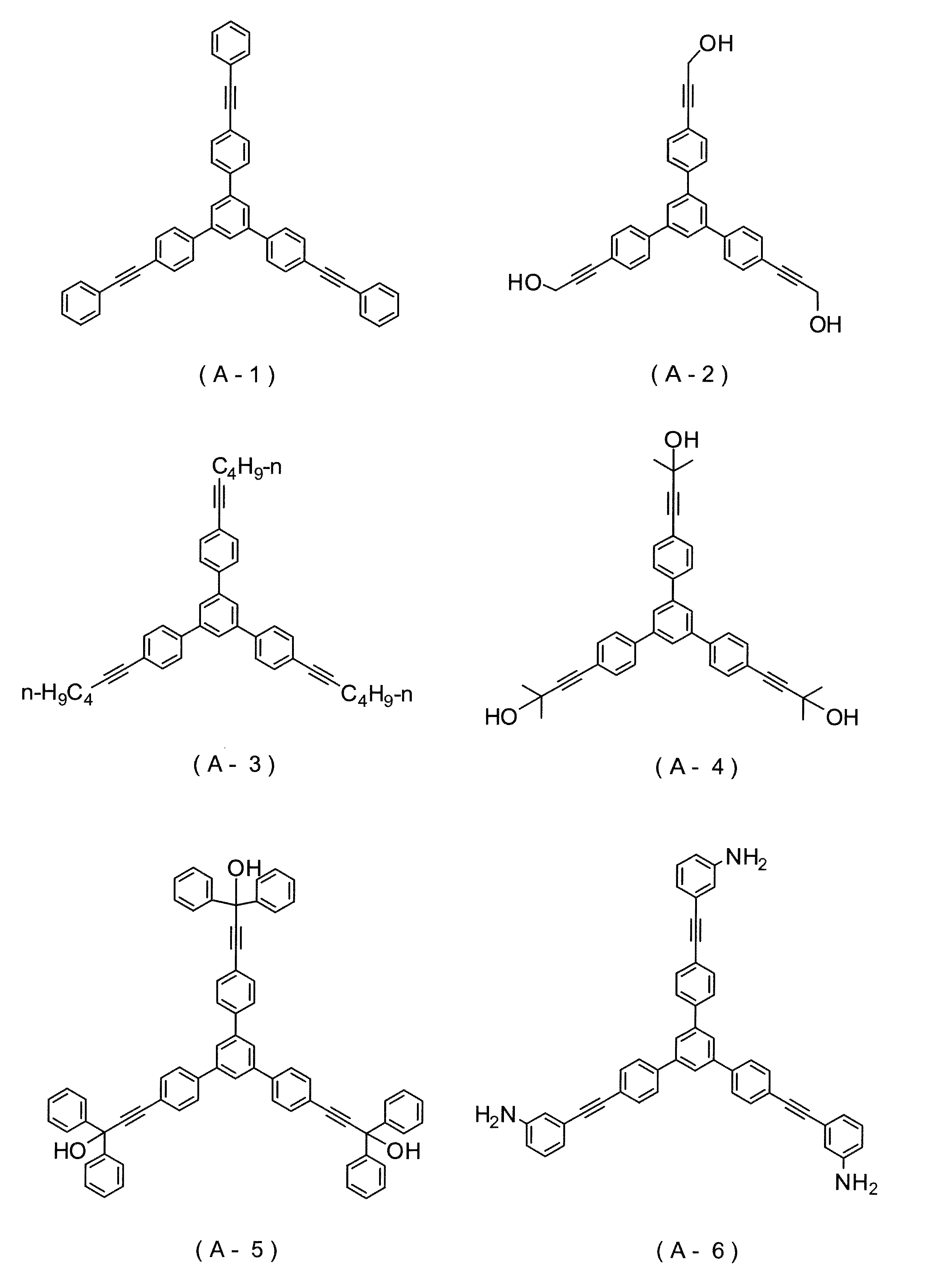
温度計を備えたセパラブルフラスコに、窒素雰囲気下で、1,3,5-トリス(4’-ブロモビフェニル-4-イル)ベンゼン100質量部、トリメチルシリルアセチレン42質量部、ジクロロビストリフェニルホスフィンパラジウム(II)5質量部、ヨウ化銅(I)2質量部、トリエチルアミン100質量部及び溶媒としてのテトラヒドロフラン600質量部を混合し、攪拌しつつ、70℃で4時間反応し反応液を得た。この反応液をろ過後、メタノールを加えて再沈殿を行い、得られた沈殿物を酢酸エチルに溶解し、希塩酸、炭酸水素ナトリウム水溶液で順次洗浄した後、有機層を濃縮して乾固物を得た。次に、得られた乾固物に炭酸カリウム80質量部、テトラヒドロフラン400質量部及びメタノール150質量部を加え、室温で4時間反応させた。得られた反応液をろ過した後、酢酸エチルを加え、希塩酸及び炭酸水素ナトリウム水溶液で順次洗浄した後、有機層を濃縮して、下記式で表される化合物(A-7)を得た。
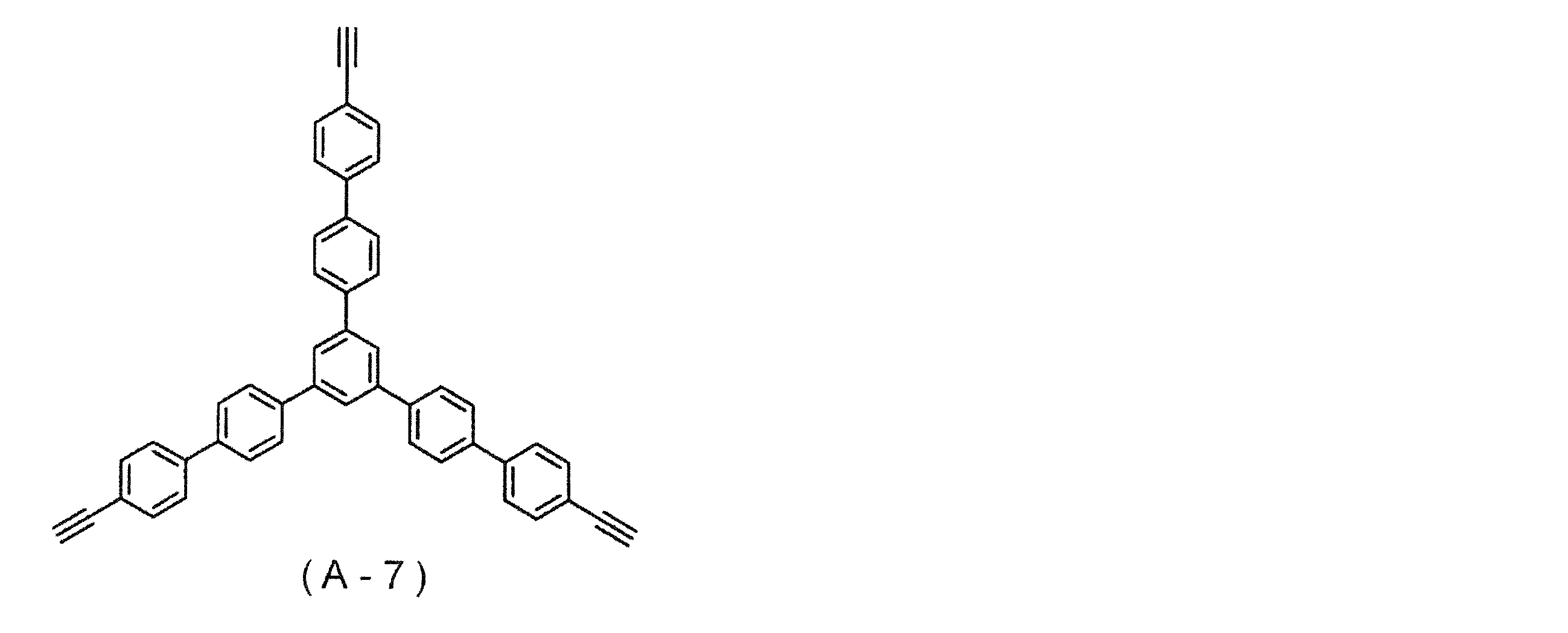
温度計を備えたセパラブルフラスコに、窒素雰囲気下で、2,7-ジヒドロキシナフタレン100質量部、ホルマリン30質量部、p-トルエンスルホン酸1質量部、及びプロピレングリコールモノメチルエーテル150質量部を仕込み、攪拌しつつ80℃で6時間重合させて反応液を得た。得られた反応液を酢酸n-ブチル100質量部で希釈し、多量の水/メタノール(質量比:1/2)混合溶媒で有機層を洗浄した。得られた有機層から溶媒を留去して、下記式(a-1)で表される構造単位を有する重合体である化合物(a-1)を得た。この化合物(a-1)のMwは、1,800であった。

膜形成用組成物を構成する[A]化合物以外の成分について以下に示す。
B-1: シクロヘキサノン
C-1:ビス(t-ブチルフェニル)ヨードニウムノナフルオロn-ブタンスルホネート(下記式(C-1)で表される化合物)
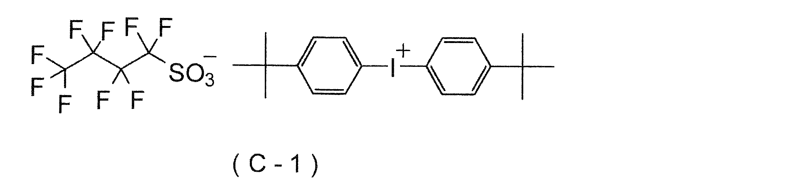
D-1:三和ケミカル社の「ニカラックN-2702」(下記式(D-1)で表される化合物)
D-2:4,4’-(1-(4-(1-(4-ヒドロキシ-3,5-ビス(メトキシメチル)フェニル)-1-メチルエチル)フェニル)エチリデン)ビス(2,6-ビス(メトキシメチル)フェノール(下記式(D-2)で表される化合物)
D-3:1,3-ジ(1,1,1,3,3,3-ヘキサフルオロプロパン-2-イルオキシカルボニル)ベンゼン(下記式(D-3)で表される化合物)
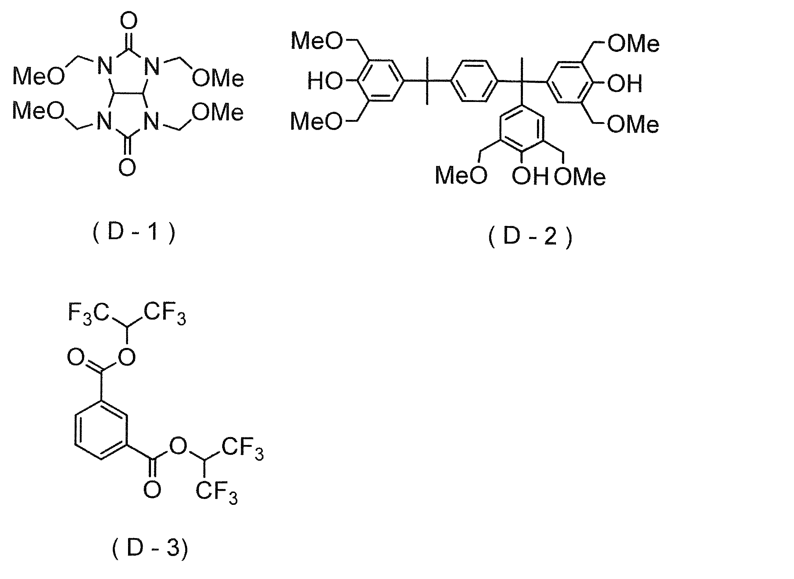
[A]化合物としての(A-1)10質量部及び[B]溶媒としての(B-1)100質量部を混合して溶液を得た。この溶液を孔径0.1μmのメンブランフィルターでろ過することにより膜形成用組成物(J-1)を調製した。
下記表1に示す種類及び含有量の各成分を用いた以外は、実施例1と同様にして、膜形成用組成物(J-2)~(J-9)及び(CJ-1)を調製した。なお、表1中の「-」は、該当する成分を用いなかったことを示す。
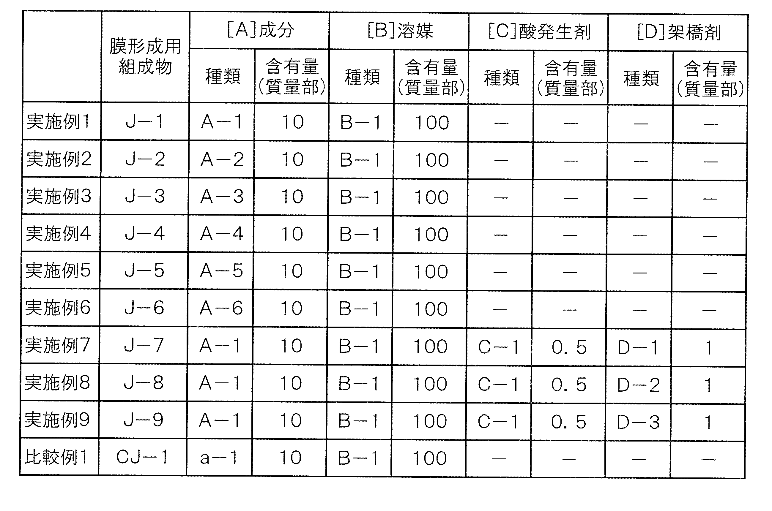
下記表2に示す種類及び含有量の各成分を用いた以外は、実施例1と同様にして、膜形成用組成物(J-10)~(J-13)を調製した。なお、表2中の「-」は、該当する成分を用いなかったことを示す。
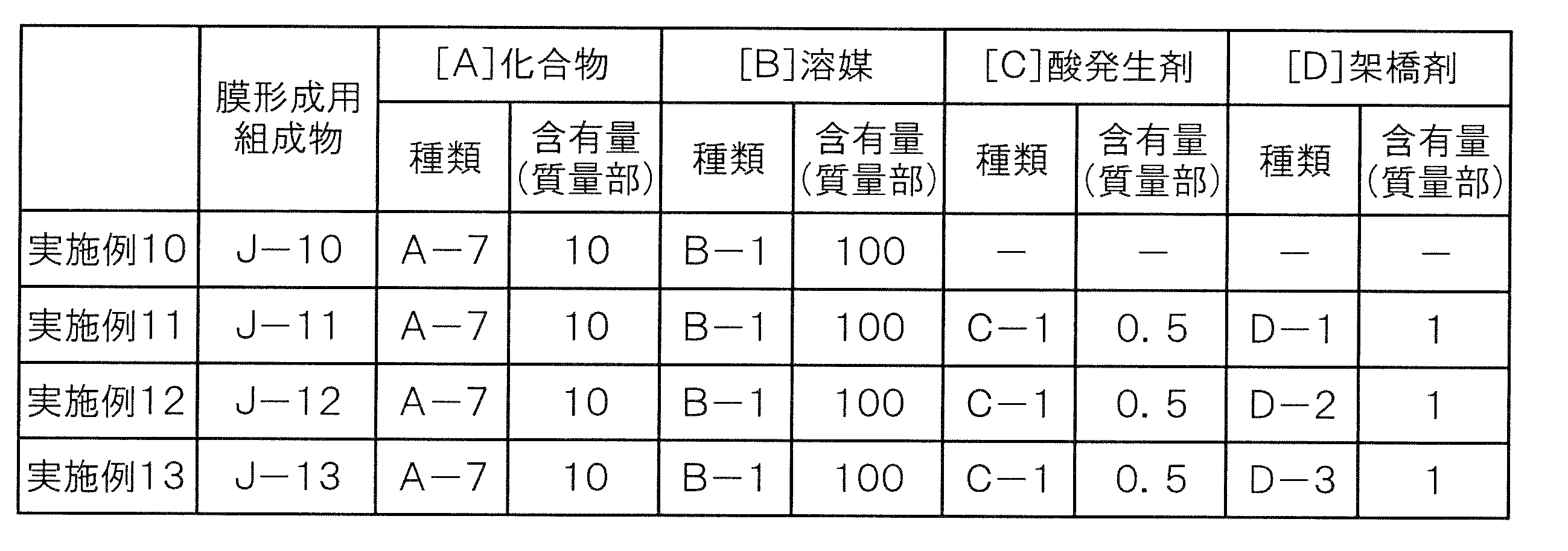
上記得られた膜形成用組成物又はそれらから得られたレジスト下層膜付き基板を用い、下記項目について、下記方法で評価を行った。評価結果を表2に示す。
上記調製した各膜形成用組成物を、基板である直径8インチのシリコンウエハ表面にスピンコートして塗膜を形成した後、この塗膜を350℃で2分間、空気中で焼成し、膜厚250nmのレジスト下層膜を形成した。分光エリプソメータ(J.A.WOOLLAM社の「M2000D」)を用い、形成されたレジスト下層膜の波長193nmにおける屈折率及び吸光係数を測定した。このとき、屈折率が1.3以上1.6以下かつ吸光係数が0.2以上0.8以下の場合、「良好」と評価できる。
まず、スピンコート法により、直径8インチのシリコンウエハ上に、膜形成用組成物をスピンコートして、膜厚300nmの下層膜を形成した。その後、この下層膜を、エッチング処理(圧力:0.03Torr、高周波電力:3000W、Ar/CF4=40/100sccm、基板温度:20℃)し、エッチング処理後の下層膜の膜厚を測定した。そして、膜厚の減少量と処理時間との関係からエッチングレート(nm/分)を算出し、比較例に対する比率を算出した。この値が小さいほど、エッチング耐性が良好である。
直径8インチのシリコンウエハ上に、各膜形成用組成物をスピンコートして塗膜(レジスト下層膜)を形成し、この塗膜の膜厚を上記分光エリプソメータを用いて測定した(この測定値をXとする)。次に、このレジスト下層膜を350℃で120秒間加熱し、加熱後のレジスト下層膜の膜厚を上記分光エリプソメータを用いて測定した(この測定値をYとする)。そして、加熱前後のレジスト下層膜の膜厚減少率△FT(%)(△FT(%)=100×(X-Y)/X)を算出し、この算出値を耐熱性(%)とした。なお、耐熱性(%)の値が小さいほど、レジスト下層膜の加熱時に発生する昇華物や膜分解物が少なく、耐熱性が高く、良好であることを表している。
幅42nm、ピッチ84nm、深さ180nmのトレンチ(アスペクト比:4.3)、幅100nm、ピッチ150nm、深さ180nmのトレンチ(アスペクト比:1.8)、幅5μm、深さ180nmのトレンチ(オープンスペース)(アスペクト比:0.036)が混在するSiO2段差基板(互いに異なるアスペクト比における最大値と最小値の比:119)上に、上記実施例及び比較例の膜形成用組成物をそれぞれ塗布した。その後、大気雰囲気下にて、250℃で60秒間焼成(ベーク)して、膜厚200nmのレジスト下層膜を形成した。このレジスト下層膜の形状を走査型電子顕微鏡(S-4800、日立ハイテック製)にて観察し、Trench又はスペース上におけるレジスト下層膜の膜厚の最大値と最小値の差(ΔFT)を測定した。平坦性はこのΔFTが20nm未満の場合は「A」(良好)と、20nm以上の場合は「B」(不良)と評価した。
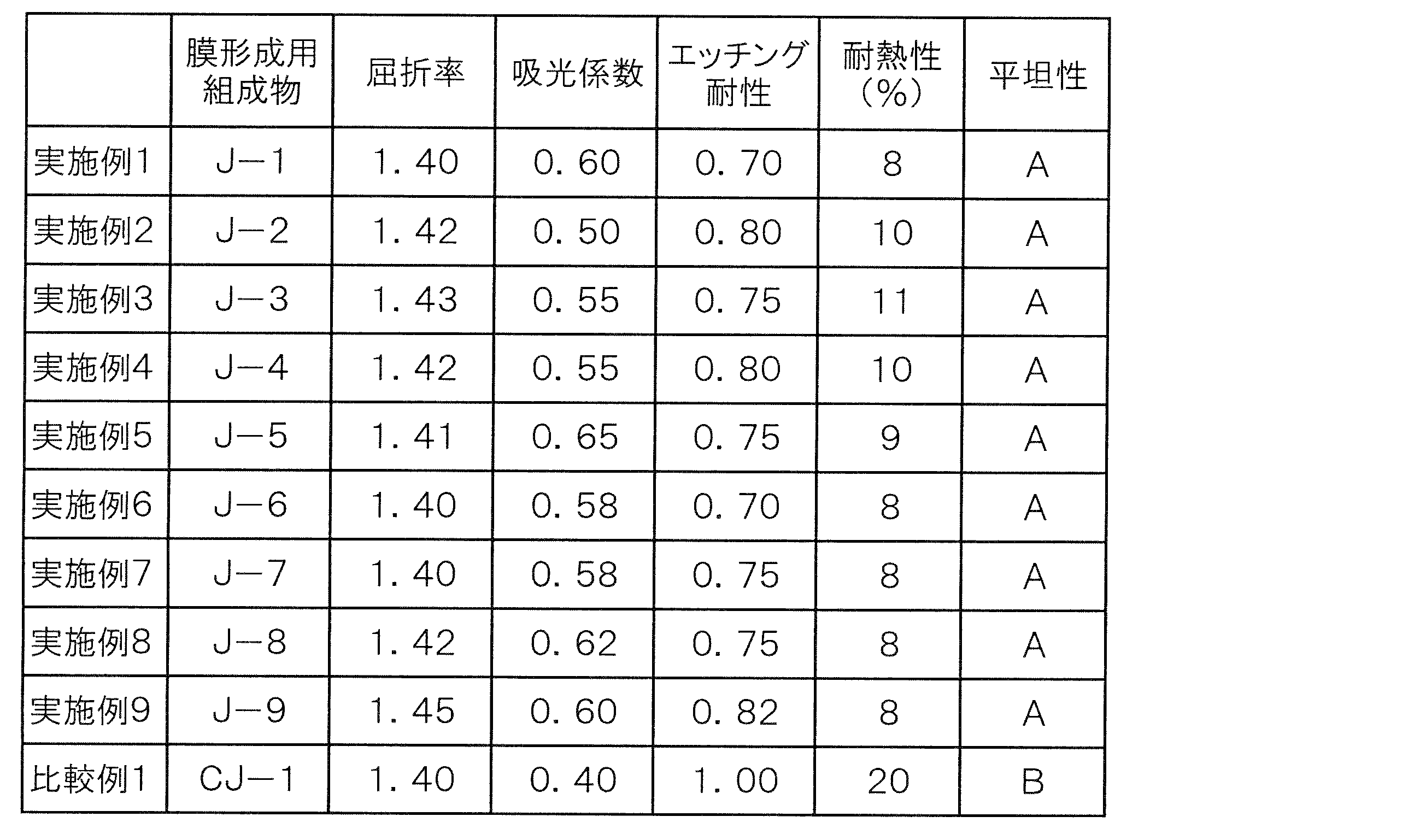
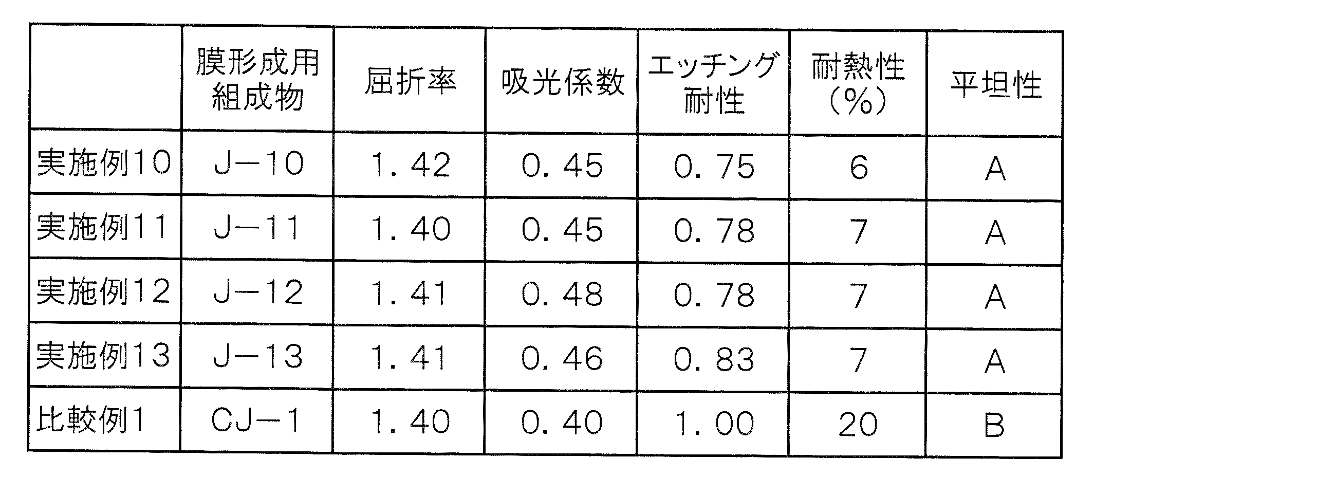
Claims (10)
- 下記式(1)で表される化合物及び溶媒を含有する膜形成用組成物。
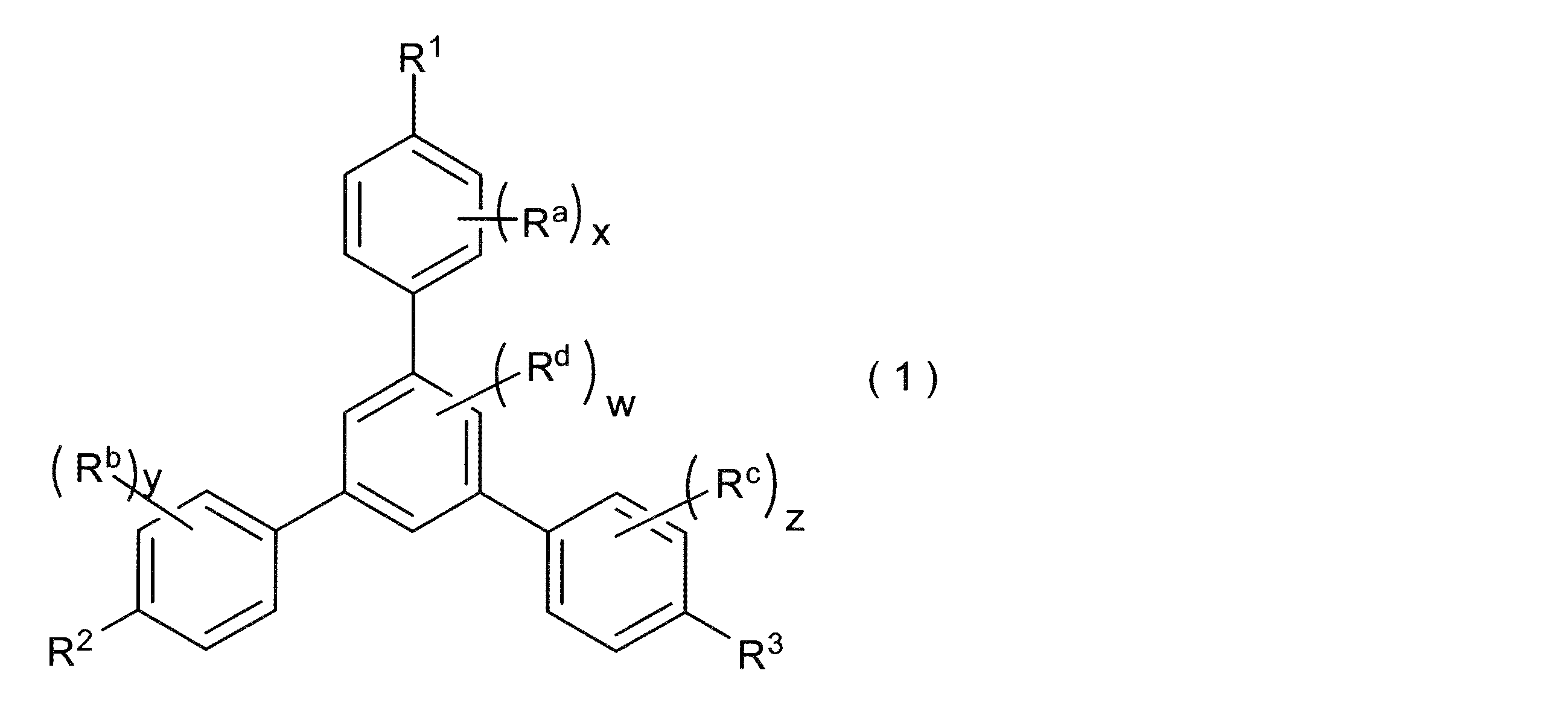
(式(1)中、R1、R2及びR3は、下記式(a)で表される基である。R1、R2及びR3は、同一でも異なっていてもよい。Ra、Rb、Rc及びRdは、それぞれ独立して、ハロゲン原子、ヒドロキシ基、アミノ基若しくはスルファニル基又は芳香環を含まない炭素数1~20の1価の有機基である。x、y及びzは、それぞれ独立して、0~4の整数である。wは、0~3の整数である。Ra~Rdがそれぞれ複数の場合、複数のRaは同一でも異なっていてもよく、複数のRbは同一でも異なっていてもよく、複数のRcは同一でも異なっていてもよく、複数のRdは同一でも異なっていてもよい。)

(式(a)中、RAは、水素原子、アリール基、又はヒドロキシ基とアリール基との少なくともいずれかで置換された若しくは非置換のアルキル基である。RBは、単結合又はアリーレン基である。上記アリール基及びアリーレン基の芳香環上の水素原子の一部又は全部はハロゲン原子、ヒドロキシ基、アミノ基若しくはスルファニル基又は芳香環を含まない炭素数1~20の1価の有機基で置換されていてもよい。) - 上記化合物の分子量が、400以上1,000以下である請求項1に記載の膜形成用組成物。
- 架橋剤をさらに含有する請求項1に記載の膜形成用組成物。
- 上記化合物の炭素含有率が50atom%以上である請求項1に記載の膜形成用組成物。
- レジスト下層膜形成用である請求項1に記載の膜形成用組成物。
- 請求項5に記載の膜形成用組成物により形成されるレジスト下層膜。
- 基板の上面側に塗膜を形成する工程、及び
上記塗膜を焼成する工程
を備え、
上記塗膜を請求項5に記載の膜形成用組成物により形成するレジスト下層膜の形成方法。 - レジスト下層膜の上面側にレジストパターンを形成する工程、及び
上記レジストパターンをマスクとし、上記レジスト下層膜及び基板を順次エッチングする工程
を備え、
上記レジスト下層膜を請求項7に記載のレジスト下層膜の形成方法により形成するパターン形成方法。 - 上記レジストパターン形成工程において、上記レジスト下層膜の上面側に中間層を形成し、この中間層の上面側にレジストパターンを形成し、
上記エッチング工程において、さらに中間層をエッチングする請求項8に記載のパターン形成方法。 - 下記式(1’)で表される化合物。

(式(1’)中、R1、R2及びR3は、下記式(a’)で表される基である。R1、R2及びR3は、同一でも異なっていてもよい。Ra’、Rb’、Rc’及びRd’は、それぞれ独立して、ハロゲン原子、ヒドロキシ基、アミノ基若しくはスルファニル基又は芳香環を含まない炭素数1~20の1価の有機基である。x’、y’及びz’は、それぞれ独立して、0~4の整数である。w’は、0~3の整数である。Ra’~Rd’がそれぞれ複数の場合、複数のRa’は同一でも異なっていてもよく、複数のRb’は同一でも異なっていてもよく、複数のRc’は同一でも異なっていてもよく、複数のRd’は同一でも異なっていてもよい。)

(式(a’)中、RA’は、水素原子、アリール基、又はヒドロキシ基とアリール基との少なくともいずれかで置換された若しくは非置換のアルキル基である。RB’は、単結合又はアリーレン基である。上記アリール基及びアリーレン基の芳香環上の水素原子の一部又は全部はハロゲン原子、ヒドロキシ基、アミノ基若しくはスルファニル基又は芳香環を含まない炭素数1~20の1価の有機基で置換されていてもよい。但し、上記化合物における3つのRA’のうちの少なくとも1つは水素原子である。)
Priority Applications (3)
| Application Number | Priority Date | Filing Date | Title |
|---|---|---|---|
| JP2015523959A JP6361657B2 (ja) | 2013-06-24 | 2014-06-09 | 膜形成用組成物、レジスト下層膜及びその形成方法、並びにパターン形成方法 |
| KR1020157036058A KR102222665B1 (ko) | 2013-06-24 | 2014-06-09 | 막 형성용 조성물, 레지스트 하층막 및 그의 형성 방법, 패턴 형성 방법 및 화합물 |
| US14/959,223 US9581905B2 (en) | 2013-06-24 | 2015-12-04 | Composition for film formation, resist underlayer film and forming method thereof, pattern-forming method and compound |
Applications Claiming Priority (2)
| Application Number | Priority Date | Filing Date | Title |
|---|---|---|---|
| JP2013132125 | 2013-06-24 | ||
| JP2013-132125 | 2013-06-24 |
Related Child Applications (1)
| Application Number | Title | Priority Date | Filing Date |
|---|---|---|---|
| US14/959,223 Continuation US9581905B2 (en) | 2013-06-24 | 2015-12-04 | Composition for film formation, resist underlayer film and forming method thereof, pattern-forming method and compound |
Publications (1)
| Publication Number | Publication Date |
|---|---|
| WO2014208324A1 true WO2014208324A1 (ja) | 2014-12-31 |
Family
ID=52141669
Family Applications (1)
| Application Number | Title | Priority Date | Filing Date |
|---|---|---|---|
| PCT/JP2014/065265 Ceased WO2014208324A1 (ja) | 2013-06-24 | 2014-06-09 | 膜形成用組成物、レジスト下層膜及びその形成方法、パターン形成方法並びに化合物 |
Country Status (5)
| Country | Link |
|---|---|
| US (1) | US9581905B2 (ja) |
| JP (1) | JP6361657B2 (ja) |
| KR (1) | KR102222665B1 (ja) |
| TW (1) | TWI641580B (ja) |
| WO (1) | WO2014208324A1 (ja) |
Cited By (29)
| Publication number | Priority date | Publication date | Assignee | Title |
|---|---|---|---|---|
| KR20160107102A (ko) * | 2015-03-03 | 2016-09-13 | 제이에스알 가부시끼가이샤 | 레지스트 하층막 형성용 조성물, 레지스트 하층막 및 패터닝된 기판의 제조 방법 |
| KR20190024779A (ko) | 2017-08-30 | 2019-03-08 | 신에쓰 가가꾸 고교 가부시끼가이샤 | 유기막 형성용 조성물, 반도체 장치 제조용 기판, 유기막의 형성 방법, 패턴 형성 방법 및 중합체 |
| KR20190024785A (ko) | 2017-08-28 | 2019-03-08 | 신에쓰 가가꾸 고교 가부시끼가이샤 | 유기막 형성용 조성물, 반도체 장치 제조용 기판, 유기막의 형성 방법, 패턴 형성 방법 및 중합체 |
| KR20190050531A (ko) * | 2017-11-03 | 2019-05-13 | 삼성에스디아이 주식회사 | 중합체, 유기막 조성물 및 패턴 형성 방법 |
| EP3550362A1 (en) | 2018-03-28 | 2019-10-09 | Shin-Etsu Chemical Co., Ltd. | Compound, composition for forming organic film, substrate for manufacturing semiconductor apparatus, method for forming organic film, and patterning process |
| WO2019208212A1 (ja) * | 2018-04-23 | 2019-10-31 | Jsr株式会社 | レジスト下層膜形成用組成物、レジスト下層膜及びその形成方法並びにパターン形成方法 |
| EP3584238A1 (en) | 2018-06-20 | 2019-12-25 | Shin-Etsu Chemical Co., Ltd. | Compound, method for manufacturing the compound, and composition for forming organic film |
| EP3584240A1 (en) | 2018-06-20 | 2019-12-25 | Shin-Etsu Chemical Co., Ltd. | Compound and composition for forming organic film |
| WO2020031733A1 (ja) * | 2018-08-09 | 2020-02-13 | Jsr株式会社 | レジスト下層膜形成用組成物、レジスト下層膜及びその形成方法、パターン形成方法並びに化合物及びその製造方法 |
| JP2020029558A (ja) * | 2018-08-21 | 2020-02-27 | 三星エスディアイ株式会社Samsung SDI Co., Ltd. | 重合体、有機膜組成物、およびパターン形成方法 |
| EP3623867A1 (en) | 2018-09-13 | 2020-03-18 | Shin-Etsu Chemical Co., Ltd. | Patterning process |
| JP2020071486A (ja) * | 2018-11-02 | 2020-05-07 | ローム アンド ハース エレクトロニック マテリアルズ エルエルシーRohm and Haas Electronic Materials LLC | 芳香族下層 |
| EP3725772A1 (en) | 2019-04-16 | 2020-10-21 | Shin-Etsu Chemical Co., Ltd. | Compounds and materials for forming organic film, substrate for manufacturing semiconductor device, method for forming organic film, and patterning process |
| EP3725773A1 (en) | 2019-04-16 | 2020-10-21 | Shin-Etsu Chemical Co., Ltd. | Compounds and materials for forming organic film, substrate for manufacturing semiconductor device, method for forming organic film, and patterning process |
| KR20200136836A (ko) | 2019-05-27 | 2020-12-08 | 신에쓰 가가꾸 고교 가부시끼가이샤 | 유기막 형성용 재료, 반도체 장치 제조용 기판, 유기막의 형성 방법, 및 패턴 형성 방법 |
| EP3761115A1 (en) | 2019-07-05 | 2021-01-06 | Shin-Etsu Chemical Co., Ltd. | Composition for forming organic film, substrate for manufacturing semiconductor device, method for forming organic film, patterning process, and polymer |
| EP3885830A1 (en) | 2020-03-23 | 2021-09-29 | Shin-Etsu Chemical Co., Ltd. | Material for forming organic film, substrate for manufacturing semiconductor device, method for forming organic film, patterning process, and compound for forming organic film |
| JP2021175801A (ja) * | 2020-05-02 | 2021-11-04 | ローム アンド ハース エレクトロニック マテリアルズ エルエルシーRohm and Haas Electronic Materials LLC | コーティング組成物及び電子デバイスを形成する方法 |
| JP2021175802A (ja) * | 2020-05-02 | 2021-11-04 | ローム アンド ハース エレクトロニック マテリアルズ エルエルシーRohm and Haas Electronic Materials LLC | コーティング組成物及び電子デバイスを形成する方法 |
| KR20220045560A (ko) | 2020-10-05 | 2022-04-12 | 신에쓰 가가꾸 고교 가부시끼가이샤 | 유기막 형성용 재료, 반도체 장치 제조용 기판, 유기막의 형성 방법, 패턴 형성 방법 및 유기막 형성용 화합물 |
| EP4043448A1 (en) | 2021-02-15 | 2022-08-17 | Shin-Etsu Chemical Co., Ltd. | Material for forming organic film, substrate for manufacturing semiconductor device, method for forming organic film, patterning process, and compound for forming organic film |
| EP4187320A1 (en) | 2021-11-25 | 2023-05-31 | Shin-Etsu Chemical Co., Ltd. | Material for forming organic film, substrate for manufacturing semiconductor device, method for forming organic film, and patterning process |
| EP4418305A1 (en) | 2023-02-15 | 2024-08-21 | Shin-Etsu Chemical Co., Ltd. | Patterning process |
| JP2024115540A (ja) * | 2023-02-14 | 2024-08-26 | 三星エスディアイ株式会社 | ハードマスク組成物、ハードマスク層およびパターン形成方法 |
| JP2024161888A (ja) * | 2023-05-08 | 2024-11-20 | 三星エスディアイ株式会社 | ハードマスク組成物、ハードマスク層およびパターン形成方法 |
| EP4600734A1 (en) | 2024-01-31 | 2025-08-13 | Shin-Etsu Chemical Co., Ltd. | Pattern forming method and laminate |
| EP4660703A2 (en) | 2024-05-29 | 2025-12-10 | Shin-Etsu Chemical Co., Ltd. | Metal-containing film patterning process |
| EP4722194A2 (en) | 2024-10-07 | 2026-04-08 | Shin-Etsu Chemical Co., Ltd. | Material for forming organic film, substrate for manufacturing semiconductor device, method for forming organic film, patterning process, compound for forming organic film, and aromatic carboxylic anhydride |
| US12619150B2 (en) | 2021-02-15 | 2026-05-05 | Shin-Etsu Chemical Co., Ltd. | Material for forming organic film, substrate for manufacturing semiconductor device, method for forming organic film, patterning process, and compound for forming organic film |
Families Citing this family (9)
| Publication number | Priority date | Publication date | Assignee | Title |
|---|---|---|---|---|
| JP2761900B2 (ja) | 1988-09-27 | 1998-06-04 | 大日本印刷株式会社 | 絵柄フィルム歪補正方法および装置 |
| KR102539857B1 (ko) * | 2016-04-29 | 2023-06-07 | 동우 화인켐 주식회사 | 하드마스크용 조성물 |
| WO2018051930A1 (ja) * | 2016-09-16 | 2018-03-22 | Jsr株式会社 | レジスト下層膜形成用組成物、レジスト下層膜及びその形成方法並びにパターニングされた基板の製造方法 |
| CN110527520B (zh) * | 2018-05-25 | 2022-07-05 | 石家庄诚志永华显示材料有限公司 | 一种液晶化合物及液晶组合物 |
| US12411409B2 (en) | 2018-11-02 | 2025-09-09 | Rohm And Haas Electronic Materials Llc | Aromatic underlayer |
| TWI838503B (zh) | 2019-03-28 | 2024-04-11 | 日商Jsr股份有限公司 | 抗蝕劑底層膜形成用組成物、抗蝕劑底層膜、抗蝕劑底層膜的形成方法、經圖案化的基板的製造方法及化合物 |
| KR102516193B1 (ko) * | 2019-09-17 | 2023-03-29 | 삼성에스디아이 주식회사 | 하드마스크 조성물, 하드마스크 층 및 패턴 형성 방법 |
| JP7445583B2 (ja) * | 2020-11-25 | 2024-03-07 | 信越化学工業株式会社 | レジスト下層膜材料、パターン形成方法、及びレジスト下層膜形成方法 |
| TW202302522A (zh) * | 2021-03-02 | 2023-01-16 | 日商三菱瓦斯化學股份有限公司 | 微影術用膜形成材料、組成物、微影術用下層膜,及圖型形成方法 |
Citations (5)
| Publication number | Priority date | Publication date | Assignee | Title |
|---|---|---|---|---|
| JP2004504424A (ja) * | 2000-07-19 | 2004-02-12 | ハネウエル・インターナシヨナル・インコーポレーテツド | ポリマーネットワークを有する低誘電率材料 |
| JP2004177668A (ja) * | 2002-11-27 | 2004-06-24 | Tokyo Ohka Kogyo Co Ltd | 多層レジストプロセス用下層膜形成材料およびこれを用いた配線形成方法 |
| US20040198850A1 (en) * | 2002-12-31 | 2004-10-07 | International Business Machines Corporation | Porous composition of matter, and method of making same |
| JP2010043176A (ja) * | 2008-08-12 | 2010-02-25 | Fujifilm Corp | 膜形成用組成物、絶縁膜、および電子デバイス |
| WO2012103309A2 (en) * | 2011-01-26 | 2012-08-02 | The University Of North Carolina At Chapel Hill | Polymeric systems containing chromophoric units for photo-driven catalysis and water splitting |
Family Cites Families (8)
| Publication number | Priority date | Publication date | Assignee | Title |
|---|---|---|---|---|
| EP0854849B1 (en) * | 1995-09-12 | 2001-10-31 | The Dow Chemical Company | Ethynyl substituted aromatic compounds, synthesis, polymers and uses thereof |
| JP4729803B2 (ja) | 2001-03-29 | 2011-07-20 | Jsr株式会社 | 多層レジストプロセス用下層膜形成組成物 |
| JP4292910B2 (ja) | 2002-07-31 | 2009-07-08 | Jsr株式会社 | アセナフチレン誘導体、重合体および反射防止膜形成組成物 |
| TWI258635B (en) * | 2002-11-27 | 2006-07-21 | Tokyo Ohka Kogyo Co Ltd | Undercoating material for wiring, embedded material, and wiring formation method |
| JP2004250585A (ja) * | 2003-02-20 | 2004-09-09 | Asahi Glass Co Ltd | ケイ素含有芳香族ポリマーおよびその用途 |
| US20070195682A1 (en) * | 2006-02-21 | 2007-08-23 | Duerig Urs T | Method for high density data storage and imaging |
| JP2009079137A (ja) * | 2007-09-26 | 2009-04-16 | Fujifilm Corp | 膜形成用組成物及び膜の製造方法 |
| JP5229278B2 (ja) * | 2010-06-21 | 2013-07-03 | 信越化学工業株式会社 | ナフタレン誘導体、レジスト下層膜材料、レジスト下層膜形成方法及びパターン形成方法 |
-
2014
- 2014-06-09 JP JP2015523959A patent/JP6361657B2/ja active Active
- 2014-06-09 WO PCT/JP2014/065265 patent/WO2014208324A1/ja not_active Ceased
- 2014-06-09 KR KR1020157036058A patent/KR102222665B1/ko active Active
- 2014-06-18 TW TW103121010A patent/TWI641580B/zh active
-
2015
- 2015-12-04 US US14/959,223 patent/US9581905B2/en active Active
Patent Citations (5)
| Publication number | Priority date | Publication date | Assignee | Title |
|---|---|---|---|---|
| JP2004504424A (ja) * | 2000-07-19 | 2004-02-12 | ハネウエル・インターナシヨナル・インコーポレーテツド | ポリマーネットワークを有する低誘電率材料 |
| JP2004177668A (ja) * | 2002-11-27 | 2004-06-24 | Tokyo Ohka Kogyo Co Ltd | 多層レジストプロセス用下層膜形成材料およびこれを用いた配線形成方法 |
| US20040198850A1 (en) * | 2002-12-31 | 2004-10-07 | International Business Machines Corporation | Porous composition of matter, and method of making same |
| JP2010043176A (ja) * | 2008-08-12 | 2010-02-25 | Fujifilm Corp | 膜形成用組成物、絶縁膜、および電子デバイス |
| WO2012103309A2 (en) * | 2011-01-26 | 2012-08-02 | The University Of North Carolina At Chapel Hill | Polymeric systems containing chromophoric units for photo-driven catalysis and water splitting |
Cited By (67)
| Publication number | Priority date | Publication date | Assignee | Title |
|---|---|---|---|---|
| KR102498508B1 (ko) | 2015-03-03 | 2023-02-10 | 제이에스알 가부시끼가이샤 | 레지스트 하층막 형성용 조성물, 레지스트 하층막 및 패터닝된 기판의 제조 방법 |
| JP2016167047A (ja) * | 2015-03-03 | 2016-09-15 | Jsr株式会社 | レジスト下層膜形成用組成物、レジスト下層膜及びパターニングされた基板の製造方法 |
| KR20160107102A (ko) * | 2015-03-03 | 2016-09-13 | 제이에스알 가부시끼가이샤 | 레지스트 하층막 형성용 조성물, 레지스트 하층막 및 패터닝된 기판의 제조 방법 |
| KR20190024785A (ko) | 2017-08-28 | 2019-03-08 | 신에쓰 가가꾸 고교 가부시끼가이샤 | 유기막 형성용 조성물, 반도체 장치 제조용 기판, 유기막의 형성 방법, 패턴 형성 방법 및 중합체 |
| US10998197B2 (en) | 2017-08-28 | 2021-05-04 | Shin-Etsu Chemical Co., Ltd. | Polymer and composition for forming organic film, substrate for manufacturing semiconductor apparatus, method for forming organic film, and patterning process |
| KR20190024779A (ko) | 2017-08-30 | 2019-03-08 | 신에쓰 가가꾸 고교 가부시끼가이샤 | 유기막 형성용 조성물, 반도체 장치 제조용 기판, 유기막의 형성 방법, 패턴 형성 방법 및 중합체 |
| US11181821B2 (en) | 2017-08-30 | 2021-11-23 | Shin-Etsu Chemical Co., Ltd. | Composition for forming organic film, substrate for manufacturing semiconductor apparatus, method for forming organic film, patterning process, and polymer |
| KR20190050531A (ko) * | 2017-11-03 | 2019-05-13 | 삼성에스디아이 주식회사 | 중합체, 유기막 조성물 및 패턴 형성 방법 |
| KR102149970B1 (ko) * | 2017-11-03 | 2020-08-31 | 삼성에스디아이 주식회사 | 중합체, 유기막 조성물 및 패턴 형성 방법 |
| JP2019172605A (ja) * | 2018-03-28 | 2019-10-10 | 信越化学工業株式会社 | 化合物、有機膜形成用組成物、半導体装置製造用基板、有機膜の形成方法及びパターン形成方法 |
| US11307497B2 (en) | 2018-03-28 | 2022-04-19 | Shin-Etsu Chemical Co., Ltd. | Compound, composition for forming organic film, substrate for manufacturing semiconductor apparatus, method for forming organic film, and patterning process |
| KR20190114839A (ko) | 2018-03-28 | 2019-10-10 | 신에쓰 가가꾸 고교 가부시끼가이샤 | 화합물, 유기막 형성용 조성물, 반도체 장치 제조용 기판, 유기막의 형성 방법 및 패턴 형성 방법 |
| EP3550362A1 (en) | 2018-03-28 | 2019-10-09 | Shin-Etsu Chemical Co., Ltd. | Compound, composition for forming organic film, substrate for manufacturing semiconductor apparatus, method for forming organic film, and patterning process |
| JPWO2019208212A1 (ja) * | 2018-04-23 | 2021-05-20 | Jsr株式会社 | レジスト下層膜形成用組成物、レジスト下層膜及びその形成方法並びにパターン形成方法 |
| JP7255589B2 (ja) | 2018-04-23 | 2023-04-11 | Jsr株式会社 | レジスト下層膜形成用組成物、レジスト下層膜及びその形成方法並びにパターン形成方法 |
| WO2019208212A1 (ja) * | 2018-04-23 | 2019-10-31 | Jsr株式会社 | レジスト下層膜形成用組成物、レジスト下層膜及びその形成方法並びにパターン形成方法 |
| US11022882B2 (en) | 2018-06-20 | 2021-06-01 | Shin-Etsu Chemical Co., Ltd. | Compound and composition for forming organic film |
| KR20190143410A (ko) | 2018-06-20 | 2019-12-30 | 신에쓰 가가꾸 고교 가부시끼가이샤 | 화합물, 화합물의 제조 방법 및 유기막 형성용 조성물 |
| JP7698002B2 (ja) | 2018-06-20 | 2025-06-24 | 信越化学工業株式会社 | 化合物、及び有機膜形成用組成物 |
| US10604618B2 (en) | 2018-06-20 | 2020-03-31 | Shin-Etsu Chemical Co., Ltd. | Compound, method for manufacturing the compound, and composition for forming organic film |
| KR20210130678A (ko) | 2018-06-20 | 2021-11-01 | 신에쓰 가가꾸 고교 가부시끼가이샤 | 화합물 및 유기막 형성용 조성물 |
| KR20190143412A (ko) | 2018-06-20 | 2019-12-30 | 신에쓰 가가꾸 고교 가부시끼가이샤 | 화합물 및 유기막 형성용 조성물 |
| JP2023162189A (ja) * | 2018-06-20 | 2023-11-08 | 信越化学工業株式会社 | 化合物、及び有機膜形成用組成物 |
| JP2019218336A (ja) * | 2018-06-20 | 2019-12-26 | 信越化学工業株式会社 | 化合物、化合物の製造方法及び有機膜形成用組成物 |
| EP3584240A1 (en) | 2018-06-20 | 2019-12-25 | Shin-Etsu Chemical Co., Ltd. | Compound and composition for forming organic film |
| EP3584238A1 (en) | 2018-06-20 | 2019-12-25 | Shin-Etsu Chemical Co., Ltd. | Compound, method for manufacturing the compound, and composition for forming organic film |
| WO2020031733A1 (ja) * | 2018-08-09 | 2020-02-13 | Jsr株式会社 | レジスト下層膜形成用組成物、レジスト下層膜及びその形成方法、パターン形成方法並びに化合物及びその製造方法 |
| JP7272364B2 (ja) | 2018-08-09 | 2023-05-12 | Jsr株式会社 | レジスト下層膜形成用組成物、レジスト下層膜及びその形成方法、パターン形成方法並びに化合物及びその製造方法 |
| US11880138B2 (en) | 2018-08-09 | 2024-01-23 | Jsr Corporation | Composition, pattern-forming method, and compound-producing method |
| JPWO2020031733A1 (ja) * | 2018-08-09 | 2021-08-26 | Jsr株式会社 | レジスト下層膜形成用組成物、レジスト下層膜及びその形成方法、パターン形成方法並びに化合物及びその製造方法 |
| JP2020029558A (ja) * | 2018-08-21 | 2020-02-27 | 三星エスディアイ株式会社Samsung SDI Co., Ltd. | 重合体、有機膜組成物、およびパターン形成方法 |
| EP3623867A1 (en) | 2018-09-13 | 2020-03-18 | Shin-Etsu Chemical Co., Ltd. | Patterning process |
| JP7075386B2 (ja) | 2018-11-02 | 2022-05-25 | ローム アンド ハース エレクトロニック マテリアルズ エルエルシー | 芳香族下層 |
| JP2020071486A (ja) * | 2018-11-02 | 2020-05-07 | ローム アンド ハース エレクトロニック マテリアルズ エルエルシーRohm and Haas Electronic Materials LLC | 芳香族下層 |
| EP3725773A1 (en) | 2019-04-16 | 2020-10-21 | Shin-Etsu Chemical Co., Ltd. | Compounds and materials for forming organic film, substrate for manufacturing semiconductor device, method for forming organic film, and patterning process |
| EP3725772A1 (en) | 2019-04-16 | 2020-10-21 | Shin-Etsu Chemical Co., Ltd. | Compounds and materials for forming organic film, substrate for manufacturing semiconductor device, method for forming organic film, and patterning process |
| KR20200121757A (ko) | 2019-04-16 | 2020-10-26 | 신에쓰 가가꾸 고교 가부시끼가이샤 | 유기막 형성용 재료, 반도체 장치 제조용 기판, 유기막의 형성 방법, 패턴 형성 방법, 및 유기막 형성용 화합물 |
| KR20200121758A (ko) | 2019-04-16 | 2020-10-26 | 신에쓰 가가꾸 고교 가부시끼가이샤 | 유기막 형성용 재료, 반도체 장치 제조용 기판, 유기막의 형성 방법, 패턴 형성 방법, 및 유기막 형성용 화합물 |
| US11500292B2 (en) | 2019-04-16 | 2022-11-15 | Shin-Etsu Chemical Co., Ltd. | Material for forming organic film, substrate for manufacturing semiconductor device, method for forming organic film, patterning process, and compound for forming organic film |
| US11692066B2 (en) | 2019-04-16 | 2023-07-04 | Shin-Etsu Chemical Co., Ltd. | Material for forming organic film, substrate for manufacturing semiconductor device, method for forming organic film, patterning process, and compound for forming organic film |
| KR20200136836A (ko) | 2019-05-27 | 2020-12-08 | 신에쓰 가가꾸 고교 가부시끼가이샤 | 유기막 형성용 재료, 반도체 장치 제조용 기판, 유기막의 형성 방법, 및 패턴 형성 방법 |
| US11676814B2 (en) | 2019-05-27 | 2023-06-13 | Shin-Etsu Chemical Co., Ltd. | Material for forming organic film, substrate for manufacturing semiconductor apparatus, method for forming organic film, and patterning process |
| EP3757677A1 (en) | 2019-05-27 | 2020-12-30 | Shin-Etsu Chemical Co., Ltd. | Material for forming organic film, substrate for manufacturing semiconductor apparatus, method for forming organic film, and patterning process |
| EP3761115A1 (en) | 2019-07-05 | 2021-01-06 | Shin-Etsu Chemical Co., Ltd. | Composition for forming organic film, substrate for manufacturing semiconductor device, method for forming organic film, patterning process, and polymer |
| US11635691B2 (en) | 2019-07-05 | 2023-04-25 | Shin-Etsu Chemical Co., Ltd. | Composition for forming organic film, substrate for manufacturing semiconductor device, method for forming organic film, patterning process, and polymer |
| EP3885830A1 (en) | 2020-03-23 | 2021-09-29 | Shin-Etsu Chemical Co., Ltd. | Material for forming organic film, substrate for manufacturing semiconductor device, method for forming organic film, patterning process, and compound for forming organic film |
| KR20210118747A (ko) | 2020-03-23 | 2021-10-01 | 신에쓰 가가꾸 고교 가부시끼가이샤 | 유기막 형성용 재료, 반도체 장치 제조용 기판, 유기막의 형성 방법, 패턴 형성 방법 및 유기막 형성용 화합물 |
| US11886118B2 (en) | 2020-03-23 | 2024-01-30 | Shin-Etsu Chemical Co., Ltd. | Material for forming organic film, substrate for manufacturing semiconductor device, method for forming organic film, patterning process, and compound for forming organic film |
| JP7204812B2 (ja) | 2020-05-02 | 2023-01-16 | ローム アンド ハース エレクトロニック マテリアルズ エルエルシー | コーティング組成物及び電子デバイスを形成する方法 |
| JP7204813B2 (ja) | 2020-05-02 | 2023-01-16 | ローム アンド ハース エレクトロニック マテリアルズ エルエルシー | コーティング組成物及び電子デバイスを形成する方法 |
| JP2021175802A (ja) * | 2020-05-02 | 2021-11-04 | ローム アンド ハース エレクトロニック マテリアルズ エルエルシーRohm and Haas Electronic Materials LLC | コーティング組成物及び電子デバイスを形成する方法 |
| JP2021175801A (ja) * | 2020-05-02 | 2021-11-04 | ローム アンド ハース エレクトロニック マテリアルズ エルエルシーRohm and Haas Electronic Materials LLC | コーティング組成物及び電子デバイスを形成する方法 |
| EP3985439A1 (en) | 2020-10-05 | 2022-04-20 | Shin-Etsu Chemical Co., Ltd. | Material for forming organic film, substrate for manufacturing semiconductor device, method for forming organic film, patterning process, and compound for forming organic film |
| KR20220045560A (ko) | 2020-10-05 | 2022-04-12 | 신에쓰 가가꾸 고교 가부시끼가이샤 | 유기막 형성용 재료, 반도체 장치 제조용 기판, 유기막의 형성 방법, 패턴 형성 방법 및 유기막 형성용 화합물 |
| US12379661B2 (en) | 2020-10-05 | 2025-08-05 | Shin-Etsu Chemical Co., Ltd. | Material for forming organic film, substrate for manufacturing semiconductor device, method for forming organic film, patterning process, and compound for forming organic film |
| KR20220117819A (ko) | 2021-02-15 | 2022-08-24 | 신에쓰 가가꾸 고교 가부시끼가이샤 | 유기막 형성용 재료, 반도체 장치 제조용 기판, 유기막의 형성 방법, 패턴 형성 방법 및 유기막 형성용 화합물 |
| US12619150B2 (en) | 2021-02-15 | 2026-05-05 | Shin-Etsu Chemical Co., Ltd. | Material for forming organic film, substrate for manufacturing semiconductor device, method for forming organic film, patterning process, and compound for forming organic film |
| EP4043448A1 (en) | 2021-02-15 | 2022-08-17 | Shin-Etsu Chemical Co., Ltd. | Material for forming organic film, substrate for manufacturing semiconductor device, method for forming organic film, patterning process, and compound for forming organic film |
| KR20230077675A (ko) | 2021-11-25 | 2023-06-01 | 신에쓰 가가꾸 고교 가부시끼가이샤 | 유기막 형성 재료, 반도체 장치 제조용 기판, 유기막의 형성 방법, 패턴 형성 방법 |
| EP4187320A1 (en) | 2021-11-25 | 2023-05-31 | Shin-Etsu Chemical Co., Ltd. | Material for forming organic film, substrate for manufacturing semiconductor device, method for forming organic film, and patterning process |
| JP2024115540A (ja) * | 2023-02-14 | 2024-08-26 | 三星エスディアイ株式会社 | ハードマスク組成物、ハードマスク層およびパターン形成方法 |
| JP7747794B2 (ja) | 2023-02-14 | 2025-10-01 | 三星エスディアイ株式会社 | ハードマスク組成物、ハードマスク層およびパターン形成方法 |
| EP4418305A1 (en) | 2023-02-15 | 2024-08-21 | Shin-Etsu Chemical Co., Ltd. | Patterning process |
| JP2024161888A (ja) * | 2023-05-08 | 2024-11-20 | 三星エスディアイ株式会社 | ハードマスク組成物、ハードマスク層およびパターン形成方法 |
| EP4600734A1 (en) | 2024-01-31 | 2025-08-13 | Shin-Etsu Chemical Co., Ltd. | Pattern forming method and laminate |
| EP4660703A2 (en) | 2024-05-29 | 2025-12-10 | Shin-Etsu Chemical Co., Ltd. | Metal-containing film patterning process |
| EP4722194A2 (en) | 2024-10-07 | 2026-04-08 | Shin-Etsu Chemical Co., Ltd. | Material for forming organic film, substrate for manufacturing semiconductor device, method for forming organic film, patterning process, compound for forming organic film, and aromatic carboxylic anhydride |
Also Published As
| Publication number | Publication date |
|---|---|
| TW201509875A (zh) | 2015-03-16 |
| TWI641580B (zh) | 2018-11-21 |
| KR102222665B1 (ko) | 2021-03-05 |
| US9581905B2 (en) | 2017-02-28 |
| KR20160023696A (ko) | 2016-03-03 |
| JPWO2014208324A1 (ja) | 2017-02-23 |
| JP6361657B2 (ja) | 2018-07-25 |
| US20160085152A1 (en) | 2016-03-24 |
Similar Documents
| Publication | Publication Date | Title |
|---|---|---|
| JP6361657B2 (ja) | 膜形成用組成物、レジスト下層膜及びその形成方法、並びにパターン形成方法 | |
| JP6094587B2 (ja) | レジスト下層膜形成用組成物及びパターン形成方法 | |
| CN103906740B (zh) | 酚类单体、含有该酚类单体的用于形成抗蚀剂下层膜的聚合物以及含有该聚合物的用于制备抗蚀剂下层膜的组合物 | |
| JP5821694B2 (ja) | レジスト下層膜形成用組成物及びパターン形成方法 | |
| TWI534549B (zh) | And a method for forming a photoresist underlayer film | |
| TWI765910B (zh) | 抗蝕劑底層膜形成用組成物、抗蝕劑底層膜及其形成方法以及圖案化基板的製造方法 | |
| JP6213328B2 (ja) | 膜形成用組成物、レジスト下層膜及びその形成方法並びにパターン形成方法 | |
| WO2009119201A1 (ja) | レジスト下層膜及びレジスト下層膜形成用組成物並びにレジスト下層膜形成方法 | |
| WO2013080929A1 (ja) | 多層レジストプロセスに用いられるレジスト下層膜形成用組成物、レジスト下層膜及びその形成方法、並びにパターン形成方法 | |
| JP2016167047A (ja) | レジスト下層膜形成用組成物、レジスト下層膜及びパターニングされた基板の製造方法 | |
| KR101174086B1 (ko) | 고분자, 고분자 조성물, 이를 포함하는 레지스트 하층막 조성물 및 이를 이용하는 재료의 패턴화 방법 | |
| KR102697916B1 (ko) | 레지스트 하층막 형성용 조성물, 레지스트 하층막 및 패터닝된 기판의 제조 방법 | |
| KR101832321B1 (ko) | 자가 가교형 고분자, 이를 포함하는 레지스트 하층막 조성물 및 이를 이용한 패턴 형성 방법 | |
| JP6281490B2 (ja) | レジスト下層膜形成用樹脂組成物、レジスト下層膜及びその形成方法、並びにパターン形成方法 | |
| US9447303B2 (en) | Composition for forming resist underlayer film | |
| KR101993480B1 (ko) | 레지스트 하층막 형성용 수지 조성물, 레지스트 하층막, 그의 형성 방법 및 패턴 형성 방법 |
Legal Events
| Date | Code | Title | Description |
|---|---|---|---|
| 121 | Ep: the epo has been informed by wipo that ep was designated in this application |
Ref document number: 14817476 Country of ref document: EP Kind code of ref document: A1 |
|
| ENP | Entry into the national phase |
Ref document number: 2015523959 Country of ref document: JP Kind code of ref document: A |
|
| ENP | Entry into the national phase |
Ref document number: 20157036058 Country of ref document: KR Kind code of ref document: A |
|
| NENP | Non-entry into the national phase |
Ref country code: DE |
|
| 122 | Ep: pct application non-entry in european phase |
Ref document number: 14817476 Country of ref document: EP Kind code of ref document: A1 |