WO2015004939A1 - 電子・電気機器用銅合金、電子・電気機器用銅合金薄板、電子・電気機器用導電部品及び端子 - Google Patents
電子・電気機器用銅合金、電子・電気機器用銅合金薄板、電子・電気機器用導電部品及び端子 Download PDFInfo
- Publication number
- WO2015004939A1 WO2015004939A1 PCT/JP2014/054042 JP2014054042W WO2015004939A1 WO 2015004939 A1 WO2015004939 A1 WO 2015004939A1 JP 2014054042 W JP2014054042 W JP 2014054042W WO 2015004939 A1 WO2015004939 A1 WO 2015004939A1
- Authority
- WO
- WIPO (PCT)
- Prior art keywords
- mass
- electronic
- copper alloy
- less
- ratio
- Prior art date
- Legal status (The legal status is an assumption and is not a legal conclusion. Google has not performed a legal analysis and makes no representation as to the accuracy of the status listed.)
- Ceased
Links
Images

Classifications
-
- C—CHEMISTRY; METALLURGY
- C22—METALLURGY; FERROUS OR NON-FERROUS ALLOYS; TREATMENT OF ALLOYS OR NON-FERROUS METALS
- C22C—ALLOYS
- C22C9/00—Alloys based on copper
- C22C9/04—Alloys based on copper with zinc as the next major constituent
-
- B—PERFORMING OPERATIONS; TRANSPORTING
- B22—CASTING; POWDER METALLURGY
- B22D—CASTING OF METALS; CASTING OF OTHER SUBSTANCES BY THE SAME PROCESSES OR DEVICES
- B22D7/00—Casting ingots, e.g. from ferrous metals
- B22D7/005—Casting ingots, e.g. from ferrous metals from non-ferrous metals
-
- C—CHEMISTRY; METALLURGY
- C22—METALLURGY; FERROUS OR NON-FERROUS ALLOYS; TREATMENT OF ALLOYS OR NON-FERROUS METALS
- C22C—ALLOYS
- C22C1/00—Making non-ferrous alloys
- C22C1/02—Making non-ferrous alloys by melting
-
- C—CHEMISTRY; METALLURGY
- C22—METALLURGY; FERROUS OR NON-FERROUS ALLOYS; TREATMENT OF ALLOYS OR NON-FERROUS METALS
- C22F—CHANGING THE PHYSICAL STRUCTURE OF NON-FERROUS METALS AND NON-FERROUS ALLOYS
- C22F1/00—Changing the physical structure of non-ferrous metals or alloys by heat treatment or by hot or cold working
- C22F1/08—Changing the physical structure of non-ferrous metals or alloys by heat treatment or by hot or cold working of copper or alloys based thereon
-
- C—CHEMISTRY; METALLURGY
- C23—COATING METALLIC MATERIAL; COATING MATERIAL WITH METALLIC MATERIAL; CHEMICAL SURFACE TREATMENT; DIFFUSION TREATMENT OF METALLIC MATERIAL; COATING BY VACUUM EVAPORATION, BY SPUTTERING, BY ION IMPLANTATION OR BY CHEMICAL VAPOUR DEPOSITION, IN GENERAL; INHIBITING CORROSION OF METALLIC MATERIAL OR INCRUSTATION IN GENERAL
- C23C—COATING METALLIC MATERIAL; COATING MATERIAL WITH METALLIC MATERIAL; SURFACE TREATMENT OF METALLIC MATERIAL BY DIFFUSION INTO THE SURFACE, BY CHEMICAL CONVERSION OR SUBSTITUTION; COATING BY VACUUM EVAPORATION, BY SPUTTERING, BY ION IMPLANTATION OR BY CHEMICAL VAPOUR DEPOSITION, IN GENERAL
- C23C28/00—Coating for obtaining at least two superposed coatings either by methods not provided for in a single one of groups C23C2/00 - C23C26/00 or by combinations of methods provided for in subclasses C23C and C25C or C25D
- C23C28/02—Coating for obtaining at least two superposed coatings either by methods not provided for in a single one of groups C23C2/00 - C23C26/00 or by combinations of methods provided for in subclasses C23C and C25C or C25D only coatings only including layers of metallic material
- C23C28/021—Coating for obtaining at least two superposed coatings either by methods not provided for in a single one of groups C23C2/00 - C23C26/00 or by combinations of methods provided for in subclasses C23C and C25C or C25D only coatings only including layers of metallic material including at least one metal alloy layer
-
- C—CHEMISTRY; METALLURGY
- C23—COATING METALLIC MATERIAL; COATING MATERIAL WITH METALLIC MATERIAL; CHEMICAL SURFACE TREATMENT; DIFFUSION TREATMENT OF METALLIC MATERIAL; COATING BY VACUUM EVAPORATION, BY SPUTTERING, BY ION IMPLANTATION OR BY CHEMICAL VAPOUR DEPOSITION, IN GENERAL; INHIBITING CORROSION OF METALLIC MATERIAL OR INCRUSTATION IN GENERAL
- C23C—COATING METALLIC MATERIAL; COATING MATERIAL WITH METALLIC MATERIAL; SURFACE TREATMENT OF METALLIC MATERIAL BY DIFFUSION INTO THE SURFACE, BY CHEMICAL CONVERSION OR SUBSTITUTION; COATING BY VACUUM EVAPORATION, BY SPUTTERING, BY ION IMPLANTATION OR BY CHEMICAL VAPOUR DEPOSITION, IN GENERAL
- C23C28/00—Coating for obtaining at least two superposed coatings either by methods not provided for in a single one of groups C23C2/00 - C23C26/00 or by combinations of methods provided for in subclasses C23C and C25C or C25D
- C23C28/02—Coating for obtaining at least two superposed coatings either by methods not provided for in a single one of groups C23C2/00 - C23C26/00 or by combinations of methods provided for in subclasses C23C and C25C or C25D only coatings only including layers of metallic material
- C23C28/023—Coating for obtaining at least two superposed coatings either by methods not provided for in a single one of groups C23C2/00 - C23C26/00 or by combinations of methods provided for in subclasses C23C and C25C or C25D only coatings only including layers of metallic material only coatings of metal elements only
-
- C—CHEMISTRY; METALLURGY
- C23—COATING METALLIC MATERIAL; COATING MATERIAL WITH METALLIC MATERIAL; CHEMICAL SURFACE TREATMENT; DIFFUSION TREATMENT OF METALLIC MATERIAL; COATING BY VACUUM EVAPORATION, BY SPUTTERING, BY ION IMPLANTATION OR BY CHEMICAL VAPOUR DEPOSITION, IN GENERAL; INHIBITING CORROSION OF METALLIC MATERIAL OR INCRUSTATION IN GENERAL
- C23C—COATING METALLIC MATERIAL; COATING MATERIAL WITH METALLIC MATERIAL; SURFACE TREATMENT OF METALLIC MATERIAL BY DIFFUSION INTO THE SURFACE, BY CHEMICAL CONVERSION OR SUBSTITUTION; COATING BY VACUUM EVAPORATION, BY SPUTTERING, BY ION IMPLANTATION OR BY CHEMICAL VAPOUR DEPOSITION, IN GENERAL
- C23C30/00—Coating with metallic material characterised only by the composition of the metallic material, i.e. not characterised by the coating process
- C23C30/005—Coating with metallic material characterised only by the composition of the metallic material, i.e. not characterised by the coating process on hard metal substrates
-
- H—ELECTRICITY
- H01—ELECTRIC ELEMENTS
- H01B—CABLES; CONDUCTORS; INSULATORS; SELECTION OF MATERIALS FOR THEIR CONDUCTIVE, INSULATING OR DIELECTRIC PROPERTIES
- H01B1/00—Conductors or conductive bodies characterised by the conductive materials; Selection of materials as conductors
- H01B1/02—Conductors or conductive bodies characterised by the conductive materials; Selection of materials as conductors mainly consisting of metals or alloys
- H01B1/026—Alloys based on copper
-
- Y—GENERAL TAGGING OF NEW TECHNOLOGICAL DEVELOPMENTS; GENERAL TAGGING OF CROSS-SECTIONAL TECHNOLOGIES SPANNING OVER SEVERAL SECTIONS OF THE IPC; TECHNICAL SUBJECTS COVERED BY FORMER USPC CROSS-REFERENCE ART COLLECTIONS [XRACs] AND DIGESTS
- Y10—TECHNICAL SUBJECTS COVERED BY FORMER USPC
- Y10T—TECHNICAL SUBJECTS COVERED BY FORMER US CLASSIFICATION
- Y10T428/00—Stock material or miscellaneous articles
- Y10T428/12—All metal or with adjacent metals
- Y10T428/12431—Foil or filament smaller than 6 mils
- Y10T428/12438—Composite
-
- Y—GENERAL TAGGING OF NEW TECHNOLOGICAL DEVELOPMENTS; GENERAL TAGGING OF CROSS-SECTIONAL TECHNOLOGIES SPANNING OVER SEVERAL SECTIONS OF THE IPC; TECHNICAL SUBJECTS COVERED BY FORMER USPC CROSS-REFERENCE ART COLLECTIONS [XRACs] AND DIGESTS
- Y10—TECHNICAL SUBJECTS COVERED BY FORMER USPC
- Y10T—TECHNICAL SUBJECTS COVERED BY FORMER US CLASSIFICATION
- Y10T428/00—Stock material or miscellaneous articles
- Y10T428/12—All metal or with adjacent metals
- Y10T428/12493—Composite; i.e., plural, adjacent, spatially distinct metal components [e.g., layers, joint, etc.]
- Y10T428/12708—Sn-base component
- Y10T428/12715—Next to Group IB metal-base component
-
- Y—GENERAL TAGGING OF NEW TECHNOLOGICAL DEVELOPMENTS; GENERAL TAGGING OF CROSS-SECTIONAL TECHNOLOGIES SPANNING OVER SEVERAL SECTIONS OF THE IPC; TECHNICAL SUBJECTS COVERED BY FORMER USPC CROSS-REFERENCE ART COLLECTIONS [XRACs] AND DIGESTS
- Y10—TECHNICAL SUBJECTS COVERED BY FORMER USPC
- Y10T—TECHNICAL SUBJECTS COVERED BY FORMER US CLASSIFICATION
- Y10T428/00—Stock material or miscellaneous articles
- Y10T428/12—All metal or with adjacent metals
- Y10T428/12493—Composite; i.e., plural, adjacent, spatially distinct metal components [e.g., layers, joint, etc.]
- Y10T428/12771—Transition metal-base component
- Y10T428/12861—Group VIII or IB metal-base component
- Y10T428/12882—Cu-base component alternative to Ag-, Au-, or Ni-base component
-
- Y—GENERAL TAGGING OF NEW TECHNOLOGICAL DEVELOPMENTS; GENERAL TAGGING OF CROSS-SECTIONAL TECHNOLOGIES SPANNING OVER SEVERAL SECTIONS OF THE IPC; TECHNICAL SUBJECTS COVERED BY FORMER USPC CROSS-REFERENCE ART COLLECTIONS [XRACs] AND DIGESTS
- Y10—TECHNICAL SUBJECTS COVERED BY FORMER USPC
- Y10T—TECHNICAL SUBJECTS COVERED BY FORMER US CLASSIFICATION
- Y10T428/00—Stock material or miscellaneous articles
- Y10T428/12—All metal or with adjacent metals
- Y10T428/12493—Composite; i.e., plural, adjacent, spatially distinct metal components [e.g., layers, joint, etc.]
- Y10T428/12771—Transition metal-base component
- Y10T428/12861—Group VIII or IB metal-base component
- Y10T428/12903—Cu-base component
- Y10T428/1291—Next to Co-, Cu-, or Ni-base component
-
- Y—GENERAL TAGGING OF NEW TECHNOLOGICAL DEVELOPMENTS; GENERAL TAGGING OF CROSS-SECTIONAL TECHNOLOGIES SPANNING OVER SEVERAL SECTIONS OF THE IPC; TECHNICAL SUBJECTS COVERED BY FORMER USPC CROSS-REFERENCE ART COLLECTIONS [XRACs] AND DIGESTS
- Y10—TECHNICAL SUBJECTS COVERED BY FORMER USPC
- Y10T—TECHNICAL SUBJECTS COVERED BY FORMER US CLASSIFICATION
- Y10T428/00—Stock material or miscellaneous articles
- Y10T428/26—Web or sheet containing structurally defined element or component, the element or component having a specified physical dimension
- Y10T428/263—Coating layer not in excess of 5 mils thick or equivalent
- Y10T428/264—Up to 3 mils
- Y10T428/265—1 mil or less
Definitions
- the present invention is for a Cu—Zn—Sn based electronic / electrical device used as a conductive part for an electronic / electrical device such as a connector of a semiconductor device, other terminals, a movable conductive piece of an electromagnetic relay, or a lead frame.
- the present invention relates to a copper alloy, a copper alloy thin plate for electronic / electric equipment, a conductive component for electronic / electric equipment, and a terminal using the copper alloy.
- Cu—Zn alloys have been widely used from the viewpoint of strength, workability, and cost balance.
- the surface of the base material (base plate) made of Cu—Zn alloy should be used with tin (Sn) plating.
- Sn tin
- Cu-Zn-Sn alloys are used for conductive parts such as connectors with Cu-Zn alloy as the base material and Sn plating on the surface to improve the recyclability of Sn plating material and improve the strength. There is a case.
- conductive parts for electronic and electrical equipment such as connectors are generally formed into a predetermined shape by punching a thin plate (rolled plate) having a thickness of about 0.05 to 1.0 mm, and at least a part thereof. It is manufactured by bending. In this case, it is used to contact the mating conductive member near the bent portion to obtain an electrical connection with the mating conductive member, and to maintain the contact state with the mating conductive material by the spring property of the bent portion. .
- the copper alloy for electronic / electric equipment used for such electronic / electric equipment conductive parts is excellent in conductivity, rollability and punchability. Furthermore, as described above, bending workability is applied in the case of a connector used to maintain the contact state with the mating conductive material in the vicinity of the bent portion due to the bending property of the bent portion. It is required that the stress relaxation resistance is excellent.
- Patent Documents 1 to 4 propose methods for improving the stress relaxation resistance of Cu—Zn—Sn alloys.
- Patent Document 1 states that the stress relaxation resistance can be improved by adding Ni to a Cu—Zn—Sn alloy to form a Ni—P compound, and the addition of Fe can also reduce stress relaxation. It has been shown to be effective in improving the characteristics.
- Patent Document 2 describes that the strength, elasticity, and heat resistance can be improved by adding Ni and Fe together with P to a Cu—Zn—Sn alloy to form a compound. An improvement in strength, elasticity, and heat resistance is considered to mean an improvement in stress relaxation resistance.
- Patent Document 3 describes that the stress relaxation resistance can be improved by adding Ni to the Cu—Zn—Sn alloy and adjusting the Ni / Sn ratio within a specific range. Further, it is described that the addition of a small amount of Fe is effective in improving the stress relaxation resistance.
- Patent Document 4 for lead frame materials, Ni and Fe are added together with P to a Cu—Zn—Sn alloy, and the atomic ratio of (Fe + Ni) / P is within a range of 0.2-3. It is described that the stress relaxation resistance can be improved by preparing Fe—P based compounds, Ni—P based compounds, and Fe—Ni—P based compounds.
- Patent Documents 1 and 2 disclose the individual contents of Ni, Fe, and P, and the adjustment of such individual contents does not necessarily ensure the stress relaxation resistance.
- Patent Document 3 discloses that the Ni / Sn ratio is adjusted, but the relationship between the P compound and the stress relaxation resistance is not considered at all, and sufficient and reliable stress relaxation resistance is obtained. It was not possible to improve.
- Patent Document 4 only the total amount of Fe, Ni, and P and the atomic ratio of (Fe + Ni) / P were adjusted, and the stress relaxation resistance could not be sufficiently improved.
- the conventionally proposed methods cannot sufficiently improve the stress relaxation resistance of the Cu—Zn—Sn alloy. For this reason, in the connector having the above-described structure, the residual stress is relaxed over time or in a high-temperature environment, and the contact pressure with the counterpart conductive member is not maintained, and inconveniences such as poor contact are likely to occur at an early stage. There was a problem. In order to avoid such a problem, conventionally, the thickness of the material has to be increased, leading to an increase in material cost and weight. Therefore, further reliable and sufficient improvement of the stress relaxation resistance is strongly desired.
- bending is performed so that the axis of bending is perpendicular to the rolling direction (Good Way: GW) from the viewpoint of material yield in small terminals.
- a small terminal is formed by slightly deforming in the direction (Bad way: BW) in which the bending axis is parallel to the rolling direction, and according to the material strength TS TD when a tensile test is performed in the BW direction. , Ensuring springiness. Therefore, excellent bending workability of GW and high strength of BW are required.
- Japanese Patent Laid-Open No. 05-33087 JP 2006-283060 A Japanese Patent No. 3953357 Japanese Patent No. 3717321
- the present invention has been made against the background of the above circumstances, and is a copper alloy for electronic and electrical equipment that is excellent in strength and bending workability as well as surely and sufficiently excellent in stress relaxation resistance, and It is an object of the present invention to provide a copper alloy thin plate for electronic / electric equipment, a conductive component for electronic / electric equipment, and a terminal.
- the inventors of the present invention have conducted extensive experiments and researches, and as a result, by satisfying the following conditions (a) and (b), the stress relaxation resistance is reliably and sufficiently improved, and at the same time, the strength in the BW direction and the GW direction
- the present inventors have found that a copper alloy having excellent bending workability can be obtained, and have made the present invention.
- the copper alloy for electronic / electrical equipment of the present invention has Zn exceeding 2.0 mass% to 36.5 mass% or less, Sn from 0.10 mass% to 0.90 mass%, Ni from 0.15 mass% to 1.00 mass% Less than P, 0.005 mass% or more and 0.100 mass% or less, the balance being made of Cu and inevitable impurities, and the ratio Ni / P of Ni content to P content is atomic ratio.
- the ratio Sn / Ni between the Sn content and the Ni content satisfies 0.10 ⁇ Sn / Ni ⁇ 2.90 in atomic ratio, Strength ratio TS TD / TS calculated from strength TS TD when a tensile test is performed in a direction orthogonal to the rolling direction and strength TS LD when a tensile test is performed in a direction parallel to the rolling direction LD 1. It is characterized by more than 9.
- the intensity ratio TS TD / TS LD calculated from the intensity TS LD exceeds 1.09. For this reason, since there are many ⁇ 220 ⁇ planes in a plane perpendicular to the normal direction to the rolling surface, excellent bending is achieved when bending is performed so that the bending axis is perpendicular to the rolling direction.
- strength TS TD when a tensile test is performed in a direction orthogonal to the rolling direction is increased.
- the Ni—P based precipitate is a Ni—P binary precipitate, and further, other elements such as Cu, Zn, Sn as main components, O, S, C as impurities, It may contain multi-component precipitates containing Fe, Co, Cr, Mo, Mn, Mg, Zr, Ti and the like.
- the Ni—P-based precipitate exists in the form of a phosphide or an alloy in which phosphorus is dissolved.
- the copper alloy for electronic / electrical equipment according to the second aspect of the present invention has Zn exceeding 2.0 mass% and not exceeding 36.5 mass%, Sn being 0.10 mass% to 0.90 mass%, and Ni being 0.15 mass%. Or more, less than 1.00 mass%, P containing 0.005 mass% or more and 0.100 mass% or less, and any of Fe of 0.001 mass% or more and less than 0.100 mass% and Co of 0.001 mass% or more and less than 0.100 mass% Either or both, the balance being Cu and inevitable impurities, the ratio of the total content of Ni, Fe and Co (Ni + Fe + Co) to the content of P (Ni + Fe + Co) / P is 3 in atomic ratio.
- the ratio Sn / (Ni + Fe + Co) to the total content (Ni + Fe + Co) satisfies an atomic ratio of 0.10 ⁇ Sn / (Ni + Fe + Co) ⁇ 2.90, and the total content of Fe and Co and the content of Ni
- the ratio of (Fe + Co) / Ni is an atomic ratio satisfying 0.002 ⁇ (Fe + Co) / Ni ⁇ 1.500, and the strength TS TD when a tensile test is performed in a direction orthogonal to the rolling direction, The strength ratio TS TD / TS LD calculated from the strength TS LD when the tensile test is performed in the direction parallel to the rolling direction exceeds 1.09.
- Ni is added together with P, Fe and Co are further added, and the addition ratio among Sn, Ni, Fe, Co, and P is changed. Regulate appropriately.
- [Ni, (Fe, Co)]-P-based precipitates containing one or both of Fe and Co precipitated from the parent phase (mainly ⁇ -phase) and Ni and P are appropriately present.
- the stress relaxation resistance is reliable and sufficiently excellent, and the strength (proof strength) is also high.
- [Ni, (Fe, Co)]-P-based precipitates are Ni—P, Fe—P or Co—P binary precipitates, Ni—Fe—P, Ni—Co—P.
- the [Ni, (Fe, Co)]-P precipitates exist in the form of phosphides or alloys in which phosphorus is dissolved.
- the copper alloy for electronic / electrical equipment according to the third aspect of the present invention has a strength TS TD of 500 MPa when a tensile test is performed in a direction orthogonal to the rolling direction in the above-described copper alloy for electronic / electrical equipment.
- the bending workability R / t represented by the ratio when the radius of the W bending jig is R and the thickness of the copper alloy is t when the direction perpendicular to the rolling direction is the bending axis is as described above. It is characterized by being 1 or less.
- the strength TS TD when the tensile test is performed in the direction orthogonal to the rolling direction is 500 MPa or more, so the strength is sufficient. high.
- the bending workability R / t represented by the ratio when the radius of the W bending jig is R and the thickness of the copper alloy is t is 1 or less. Therefore, it is possible to sufficiently ensure the bending workability of the GW. Therefore, the copper alloy for electronic / electrical equipment according to the third aspect is suitable for conductive parts that require particularly high strength, such as a movable conductive piece of an electromagnetic relay or a spring part of a terminal.
- the copper alloy for electronic / electrical equipment according to the fourth aspect of the present invention is the above-mentioned copper alloy for electronic / electrical equipment, wherein the average crystal grain size of the ⁇ -phase crystal grains containing Cu, Zn and Sn is 0. It is within the range of 1 ⁇ m or more and 15 ⁇ m or less, and is characterized by containing a precipitate containing at least one element selected from the group consisting of Fe, Co, and Ni and P.
- the average crystal grain size of the ⁇ -phase crystal grains containing Cu, Zn and Sn is in the range of 0.1 ⁇ m to 15 ⁇ m. Therefore, the strength (yield strength) can be further improved.
- a precipitate containing at least one element selected from the group consisting of Fe, Co, and Ni and P is included, sufficient stress relaxation resistance can be ensured.
- the copper alloy for electronic / electrical equipment according to the fifth aspect of the present invention is the above-described copper alloy for electronic / electrical equipment, wherein the ⁇ phase containing Cu, Zn and Sn is measured by EBSD method to 1000 ⁇ m 2 or more.
- the area is measured at a measurement interval of 0.1 ⁇ m, and the analysis is performed except for the measurement points having a CI value of 0.1 or less analyzed by the data analysis software OIM, and the azimuth difference between adjacent measurement points is 15 °.
- Special grain boundary length ratio (L ⁇ / L) which is the ratio of the sum L ⁇ of the grain boundary lengths of ⁇ 3, ⁇ 9, ⁇ 27a, and ⁇ 27b with respect to all the grain boundary lengths L. Is 10% or more.
- the EBSD method means an Electron Backscatter Diffraction Patterns (EBSD) method using a scanning electron microscope with a backscattered electron diffraction image system.
- OIM is data analysis software (OIM) for analyzing crystal orientation using measurement data obtained by EBSD.
- the CI value is a reliability index (Confidence Index), which is displayed as a numerical value indicating the reliability of crystal orientation determination when analyzed using the analysis software OIM Analysis (Ver. 5.3) of the EBSD device.
- OIM Revised 3rd Edition
- the copper alloy thin plate for electronic / electrical equipment of the present invention is made of the above-mentioned rolled material of copper alloy for electronic / electrical equipment and has a thickness in the range of 0.05 mm to 1.0 mm.
- the copper alloy thin plate for electronic / electric equipment having such a configuration can be suitably used for connectors, other terminals, movable conductive pieces of electromagnetic relays, lead frames, and the like.
- the base material of the Sn plating is composed of a Cu—Zn—Sn alloy containing Sn of 0.10 mass% or more and 0.90 mass% or less, so that parts such as used connectors are Sn plated. It can be recovered as Cu—Zn alloy scrap to ensure good recyclability.
- a conductive component for electronic / electrical equipment according to one aspect of the present invention is characterized by comprising the above-described copper alloy for electronic / electrical equipment.
- a terminal according to one embodiment of the present invention is characterized by being made of the above-described copper alloy for electronic and electrical equipment.
- a conductive component for electronic / electrical equipment according to another aspect of the present invention is characterized by comprising the above-described copper alloy thin plate for electronic / electrical equipment.
- a terminal according to another aspect of the present invention is characterized by comprising the above-described copper alloy thin plate for electronic / electrical equipment.
- the stress relaxation resistance is particularly excellent, the residual stress is hardly relaxed over time or in a high temperature environment, and the reliability is excellent.
- a copper alloy for electronic / electric equipment that has excellent and sufficient stress relaxation resistance and has excellent strength and bending workability, a copper alloy thin plate for electronic / electric equipment using the same, an electronic -It is possible to provide conductive parts and terminals for electrical equipment.
- the copper alloy for electronic and electric apparatuses which is one Embodiment of this invention is demonstrated.
- the copper alloy for electronic / electrical equipment according to the present embodiment is more than 2.0 mass% Zn and 36.5 mass% or less, Sn is 0.10 mass% or more and 0.90 mass% or less, Ni is 0.15 mass% or more and 1. Less than 00 mass%, P is contained in 0.005 mass% or more and 0.100 mass% or less, and the balance is composed of Cu and inevitable impurities.
- ratio Ni / P of content of Ni and content of P satisfy
- the ratio Sn / Ni between the Sn content and the Ni content is determined so as to satisfy the following expression (2) in terms of an atomic ratio. 0.10 ⁇ Sn / Ni ⁇ 2.90 (2)
- the copper alloy for electronic / electric equipment according to the present embodiment further includes one or both of Fe of 0.001 mass% or more and less than 0.100 mass% and Co of 0.001 mass% or more and less than 0.100 mass%. May be.
- the ratio of the total content of Ni, Fe and Co (Ni + Fe + Co) to the content of P (Ni + Fe + Co) / P is the atomic ratio of the following (1 ′ ) Is satisfied. 3.00 ⁇ (Ni + Fe + Co) / P ⁇ 100.00 (1 ') Further, the ratio Sn / (Ni + Fe + Co) between the Sn content and the total content of Ni, Fe and Co (Ni + Fe + Co) satisfies the following equation (2 ′) in terms of atomic ratio.
- Zn is a basic alloy element in the copper alloy which is the subject of this embodiment, and is an element effective in improving strength and springiness. Moreover, since Zn is cheaper than Cu, it is effective in reducing the material cost of the copper alloy. If Zn is 2.0 mass% or less, the effect of reducing the material cost cannot be sufficiently obtained. On the other hand, if Zn exceeds 36.5 mass%, corrosion resistance will fall and cold rolling property will also fall. Therefore, the Zn content is within the range of more than 2.0 mass% and not more than 36.5 mass%. The Zn content is preferably in the range of 5.0 mass% to 33.0 mass%, and more preferably in the range of 7.0 mass% to 27.0 mass%.
- Sn 0.10 mass% or more and 0.90 mass% or less
- Sn is effective in improving the strength and is advantageous in improving the recyclability of the Cu-Zn alloy material with Sn plating. Furthermore, it has been found by the present inventors that if Sn coexists with Ni, it contributes to the improvement of stress relaxation resistance. If Sn is less than 0.10 mass%, these effects cannot be sufficiently obtained. On the other hand, if Sn exceeds 0.90 mass%, the hot workability and the cold rollability are deteriorated. There is a possibility that cracking may occur during rolling, and the electrical conductivity also decreases. Therefore, the Sn content is set in the range of 0.10 mass% to 0.90 mass%. The Sn content is particularly preferably in the range of 0.20 mass% to 0.80 mass% even within the above range.
- Ni—P-based precipitates can be precipitated from the parent phase (mainly ⁇ -phase). Further, by adding Ni together with one or both of Fe and Co and P, the [Ni, (Fe, Co)]-P-based precipitate can be precipitated from the parent phase (mainly ⁇ -phase).
- Ni—P based precipitates or [Ni, (Fe, Co)] — P based precipitates provide an effect of pinning the grain boundaries during recrystallization. For this reason, the average crystal grain size can be reduced, and the strength, bending workability, and stress corrosion cracking resistance can be improved. Furthermore, the presence of these precipitates can greatly improve the stress relaxation resistance.
- the stress relaxation resistance can be improved even by solid solution strengthening.
- the addition amount of Ni is less than 0.15 mass%, the stress relaxation resistance cannot be sufficiently improved.
- the amount of Ni added is 1.00 mass% or more, the amount of solid solution Ni increases and the electrical conductivity decreases, and the amount of expensive Ni raw material used increases, leading to an increase in cost. Therefore, the Ni content is in the range of 0.15 mass% or more and less than 1.00 mass%.
- Ni—P-based precipitates (P: 0.005 mass% or more and 0.100 mass% or less) P has a high bondability with Ni, and if an appropriate amount of P is contained together with Ni, Ni—P-based precipitates can be precipitated, and P is added together with one or both of Fe and Co.
- the [Ni, (Fe, Co)]-P-based precipitate can be precipitated from the parent phase (mainly ⁇ -phase).
- the stress relaxation resistance can be improved by the presence of these Ni—P based precipitates or [Ni, (Fe, Co)] — P based precipitates.
- the content of P is set in the range of 0.005 mass% to 0.100 mass%.
- the content of P is particularly preferably in the range of 0.010 mass% to 0.080 mass% even within the above range.
- P is an element which is inevitably mixed from the melting raw material of the copper alloy, it is desirable to appropriately select the melting raw material in order to regulate the P content as described above. .
- Fe is not necessarily an essential additive element, but if a small amount of Fe is added together with Ni and P, a [Ni, Fe] -P-based precipitate can be precipitated from the parent phase (mainly ⁇ -phase). Further, by adding a small amount of Co, the [Ni, Fe, Co] -P-based precipitate can be precipitated from the parent phase (mainly ⁇ phase).
- the average grain size can be reduced by the effect of pinning the grain boundaries during recrystallization by these [Ni, Fe] -P based precipitates or [Ni, Fe, Co] -P based precipitates. Strength, bending workability, and stress corrosion cracking resistance can be improved.
- the presence of these precipitates can greatly improve the stress relaxation resistance.
- the addition amount of Fe is less than 0.001 mass%, the effect of further improving the stress relaxation resistance due to the addition of Fe cannot be obtained.
- the amount of Fe added is 0.100 mass% or more, the amount of solid solution Fe increases, the electrical conductivity decreases, and the cold rollability also decreases. Therefore, in the present embodiment, when Fe is added, the content of Fe is set in the range of 0.001 mass% or more and less than 0.100 mass%. In addition, it is preferable to make especially content of Fe into the range of 0.002 mass% or more and 0.080 mass% or less also in said range. Even when Fe is not actively added, Fe of less than 0.001 mass% may be contained as an impurity.
- Co is not necessarily an essential additive element, but if a small amount of Co is added together with Ni and P, a [Ni, Co] -P-based precipitate can be precipitated from the parent phase (mainly ⁇ -phase). Furthermore, by adding a small amount of Fe, the [Ni, Fe, Co] -P-based precipitate can be precipitated from the parent phase (mainly ⁇ phase). These [Ni, Fe] -P-based precipitates or [Ni, Fe, Co] -P-based precipitates can further improve the stress relaxation resistance. Here, if the amount of Co addition is less than 0.001 mass%, the effect of further improving the stress relaxation resistance by Co addition cannot be obtained.
- the Co content is set in a range of 0.001 mass% or more and less than 0.100 mass%. Even within the above range, the Co content is preferably in the range of 0.002 mass% to 0.080 mass%. Even when Co is not actively added, Co of less than 0.001 mass% may be contained as an impurity.
- the balance of the above elements may basically be Cu and inevitable impurities.
- inevitable impurities (Fe), (Co), Mg, Al, Mn, Si, Cr, Ag, Ca, Sr, Ba, Sc, Y, Hf, V, Nb, Ta, Mo, W , Re, Ru, Os, Se, Te, Rh, Ir, Pd, Pt, Au, Cd, Ga, In, Li, Ge, As, Sb, Ti, Tl, Pb, Bi, S, O, C, Be , N, H, Hg, B, Zr, rare earth, and the like.
- These inevitable impurities are desirably 0.3 mass% or less in total.
- the mutual ratio of the content of each element is an atomic ratio. It is important to regulate the ratio so as to satisfy the expressions (1), (2), or (1 ′) to (3 ′). Therefore, the reasons for limiting the equations (1), (2), and (1 ') to (3') will be described below.
- the Sn / Ni ratio is 0.10 or less, a sufficient effect of improving the stress relaxation resistance is not exhibited.
- the Sn / Ni ratio is 2.90 or more, the amount of Ni is relatively reduced, the amount of Ni—P-based precipitates is reduced, and the stress relaxation resistance is deteriorated. Therefore, the Sn / Ni ratio is regulated within the above range.
- the lower limit of the Sn / Ni ratio is desirably 0.20 or more, preferably 0.25 or more, and optimally more than 0.30, even within the above range.
- the upper limit of the Sn / Ni ratio is desirably 2.50 or less, preferably 2.00 or less, more preferably 1.50 or less, even within the above range.
- the (Ni + Fe + Co) / P ratio is 100.00 or more, the conductivity decreases due to an increase in the proportion of Ni, Fe, and Co dissolved, and the amount of expensive Co and Ni raw materials used is relatively high. Increasing costs will increase costs. Therefore, the (Ni + Fe + Co) / P ratio is regulated within the above range.
- the upper limit of the (Ni + Fe + Co) / P ratio is 50.00 or less, preferably 40.00 or less, more preferably 20.00 or less, even less than 15.00, optimally 12 even within the above range. It is desirable to set it to 0.000 or less.
- the lower limit of the Sn / (Ni + Fe + Co) ratio is desirably 0.20 or more, preferably 0.25 or more, and optimally more than 0.30, even within the above range.
- the upper limit of the Sn / (Ni + Fe + Co) ratio is desirably 2.50 or less, preferably 2.00 or less, and more preferably 1.50 or less even within the above range.
- each of the alloy elements is adjusted not only to the individual contents but also to the ratio of each element so as to satisfy the expressions (1), (2) or (1 ′) to (3 ′).
- Ni-P-based precipitates or [Ni, (Fe, Co)]-P-based precipitates are dispersed and precipitated from the parent phase (mainly ⁇ -phase). It is considered that the stress relaxation resistance is improved by the dispersion precipitation of the material.
- the copper alloy for electronic / electric equipment which is this embodiment, not only the component composition is adjusted as described above, but also the strength is defined as follows. That is, the copper alloy for electronic / electrical equipment according to the present embodiment has a strength TS TD when a tensile test is performed in a direction orthogonal to the rolling direction and a tensile test in a direction parallel to the rolling direction. of the strength TS LD, the intensity ratio TS TD / TS LD calculated from is more than a (TS TD / TS LD> 1.09 ) configuration 1.09.
- the reason why the strength is defined as described above will be described below.
- a strength ratio TS TD calculated from a strength TS TD when a tensile test is performed in a direction orthogonal to the rolling direction and a strength TS LD when a tensile test is performed in a direction parallel to the rolling direction.
- TS LD exceeds 1.09 and is preferably 1.3 or less.
- the intensity ratio TS TD / TS LD is more preferably 1.1 or more and 1.3 or less.
- the intensity ratio TS TD / TS LD is more preferably 1.12 or more and 1.3 or less.
- the strength TS TD when a tensile test is performed in the direction orthogonal to the rolling direction is 500 MPa or more, and the direction orthogonal to the rolling direction is
- the bending workability R / t represented by the ratio when the radius of the W bending jig is R and the thickness of the copper alloy is t is 1 or less.
- the crystal structure is defined as follows.
- the crystal structure preferably has a special grain boundary length ratio (L ⁇ / L) of 10% or more.
- An ⁇ phase containing Cu, Zn and Sn is measured by an EBSD method with a measurement area of 1000 ⁇ m 2 or more at a measurement interval of 0.1 ⁇ m step.
- the analysis is performed except for the measurement points having a CI value of 0.1 or less analyzed by the data analysis software OIM, and a crystal grain boundary is defined between the measurement points where the orientation difference between adjacent measurements exceeds 15 °.
- the reason for defining the crystal structure as described above will be described below.
- the special grain boundary length ratio (L ⁇ / L) which is the ratio of the sum L ⁇ of the grain boundary lengths of ⁇ 3, ⁇ 9, ⁇ 27a, and ⁇ 27b to all the grain boundary lengths L, is increased, the stress relaxation resistance The bending workability can be further improved while maintaining the characteristics.
- the special grain boundary length ratio (L ⁇ / L) is more preferably 12% or more. More preferably, it is 15% or more.
- the CI value (reliability index) when analyzed by the analysis software OIM of the EBSD device is small when the crystal pattern of the measurement point is not clear, and the analysis result is obtained when the CI value is 0.1 or less. Difficult to trust. Therefore, in the present embodiment, measurement points with low reliability whose CI value is 0.1 or less are excluded.
- the average crystal grain size of the material has some influence on the stress relaxation resistance. Generally, the smaller the average crystal grain diameter, the lower the stress relaxation resistance. In the case of the copper alloy for electronic and electrical equipment according to the present embodiment, good stress resistance is obtained by appropriately adjusting the ratio of the component composition and each alloy element and by appropriately adjusting the ratio of the special grain boundary having high crystallinity. Relaxation characteristics can be secured. For this reason, the average crystal grain size can be reduced to improve the strength and the bending workability. Therefore, it is desirable that the average crystal grain size be 15 ⁇ m or less at the stage after the finish heat treatment for recrystallization and precipitation during the manufacturing process.
- the average crystal grain size should be in the range of 0.1 ⁇ m to 10 ⁇ m, more preferably 0.1 ⁇ m to 8 ⁇ m, more preferably 0.1 ⁇ m to 5 ⁇ m. preferable.
- a molten copper alloy having the above-described component composition is melted.
- 4NCu oxygen-free copper or the like
- scrap may be used as the raw material.
- an atmospheric furnace may be used for melting, but an atmosphere furnace having a vacuum furnace, an inert gas atmosphere, or a reducing atmosphere may be used in order to suppress oxidation of the additive element.
- the copper alloy melt whose components are adjusted is cast by an appropriate casting method, for example, a batch casting method such as die casting, a continuous casting method, a semi-continuous casting method, or the like (for example, a slab-like ingot). Get.
- a batch casting method such as die casting, a continuous casting method, a semi-continuous casting method, or the like (for example, a slab-like ingot).
- Heating step: S02 Thereafter, if necessary, a homogenization heat treatment is performed in order to eliminate segregation of the ingot and make the ingot structure uniform.
- the conditions for this heat treatment are not particularly limited. Usually, the heat treatment may be performed at 600 ° C. to 950 ° C. for 5 minutes to 24 hours. If the heat treatment temperature is less than 600 ° C. or the heat treatment time is less than 5 minutes, a sufficient homogenizing effect may not be obtained. On the other hand, if the heat treatment temperature exceeds 950 ° C., a part of the segregation site may be dissolved, and if the heat treatment time exceeds 24 hours, only the cost increases.
- the cooling conditions after the heat treatment may be determined as appropriate, but usually water quenching may be performed. After the heat treatment, chamfering is performed as necessary.
- hot working may be performed on the ingot in order to increase the efficiency of roughing and make the structure uniform.
- the conditions for this hot working are not particularly limited, but it is usually preferable that the starting temperature is 600 ° C. or higher and 950 ° C. or lower, the end temperature is 300 ° C. or higher and 850 ° C. or lower, and the processing rate is 50% or higher and 99% or lower.
- the ingot heating up to the hot working start temperature may also serve as the heating step S02 described above. Cooling conditions after hot working may be determined as appropriate, but usually water quenching may be performed. In addition, after hot processing, it chamfers as needed.
- the hot working method is not particularly limited, but when the final shape is a plate or strip, it may be rolled to a thickness of about 0.5 mm to 50 mm by applying hot rolling. Further, extrusion or groove rolling may be applied when the final shape is a wire or bar, and forging or pressing may be applied when the final shape is a bulk shape.
- intermediate plastic working step S04
- the temperature condition in the intermediate plastic working step S04 is not particularly limited, but is preferably in the range of ⁇ 200 ° C. to + 200 ° C. that is cold or warm working.
- the processing rate of the intermediate plastic processing is not particularly limited, but is usually about 10% to 99%.
- the processing method is not particularly limited, but when the final shape is a plate or strip, rolling may be applied to a thickness of about 0.05 mm to 25 mm. Further, extrusion or groove rolling can be applied when the final shape is a wire or bar, and forging or pressing can be applied when the final shape is a bulk shape. Note that S02 to S04 may be repeated for thorough solution.
- Intermediate heat treatment step: S05 After the cold or warm intermediate plastic working step S04, an intermediate heat treatment that serves both as a recrystallization process and as a precipitation process is performed.
- This intermediate heat treatment is a step performed to recrystallize the structure and simultaneously disperse and precipitate Ni—P based precipitates or [Ni, (Fe, Co)] — P based precipitates.
- the conditions of the heating temperature and the heating time at which the product is produced may be applied, and it is usually from 200 ° C. to 800 ° C. and from 1 second to 24 hours.
- a batch-type heating furnace may be used, or a continuous annealing line may be used.
- the heat treatment conditions in the intermediate heat treatment step S05 vary depending on the specific means for performing the heat treatment.
- the atmosphere for the intermediate heat treatment is preferably a non-oxidizing atmosphere (nitrogen gas atmosphere, inert gas atmosphere, or reducing atmosphere).
- the cooling condition after the intermediate heat treatment is not particularly limited, but it may be normally cooled at a cooling rate of about 2000 ° C./second to 100 ° C./hour. If necessary, the intermediate plastic working step S04 and the intermediate heat treatment step S05 may be repeated a plurality of times.
- finish plastic processing is performed to the final dimension and final shape.
- the processing method in finish plastic working is not particularly limited, but when the final product form is a plate or strip, rolling (cold rolling) is applied and rolled to a thickness of about 0.05 mm to 1.0 mm. That's fine.
- forging, pressing, groove rolling, or the like may be applied depending on the final product form.
- the processing rate may be appropriately selected according to the final plate thickness and final shape, but is preferably in the range of 5% to 90%. If the processing rate is less than 5%, the effect of improving the yield strength cannot be obtained sufficiently.
- the recrystallized structure is substantially lost to form a processed structure, and the bending workability may be reduced when the direction perpendicular to the rolling direction is the bending axis.
- the processing rate is preferably 5% or more and 90% or less, and more preferably 10% or more and 90% or less. After the finish plastic working, it may be used as a product as it is, but it is usually preferable to perform a finish heat treatment.
- a finish heat treatment step S07 is performed as necessary for improving the stress relaxation resistance and low-temperature annealing hardening, or for removing residual strain.
- This finish heat treatment is desirably performed at a temperature in the range of 150 ° C. to 800 ° C. for 0.1 seconds to 24 hours.
- the heat treatment temperature is high, heat treatment for a short time may be performed, and when the heat treatment temperature is low, heat treatment for a long time may be performed.
- the temperature of the finish heat treatment is less than 150 ° C. or the finish heat treatment time is less than 0.1 seconds, there is a possibility that a sufficient effect of removing the distortion cannot be obtained.
- the finish heat treatment step S07 may be omitted.
- shape correction rolling process After the finish heat treatment step, if necessary, shape correction rolling is performed to make the internal stress uniform.
- the shape correction rolling is desirably performed at a processing rate of less than 5%. At a processing rate of 5% or more, sufficient strain is introduced and the effect of the finish heat treatment process is lost.
- the Cu—Zn—Sn alloy material in the final product form can be obtained.
- a Cu—Zn—Sn alloy thin plate strip material
- Such a thin plate may be used as it is for a conductive part for electronic / electric equipment.
- Sn plating with a film thickness of 0.1 ⁇ m or more and 10 ⁇ m or less is usually applied to one or both sides of the plate surface, and as a copper alloy strip with Sn plating, it is used for conductive parts for electronic and electrical equipment such as connectors and other terminals.
- the method of Sn plating in this case is not particularly limited, but electrolytic plating may be applied according to a conventional method, or depending on the case, reflow treatment may be performed after electrolytic plating.
- the strength ratio TS TD / TS LD is configured to exceed 1.09, so that it is normal to the rolled surface. There are many ⁇ 220 ⁇ planes in the plane perpendicular to the direction. Thereby, it has excellent bending workability when it is bent so that the axis of bending is perpendicular to the rolling direction, and strength TS when a tensile test is performed in a direction orthogonal to the rolling direction. TD increases.
- the Ni—P based precipitate or the [Ni, (Fe, Co)] — P based precipitate is appropriately present from the matrix mainly composed of ⁇ phase, the stress relaxation resistance is surely and sufficiently excellent, Moreover, the strength (proof strength) is high.
- the copper alloy thin plate for electronic / electric equipment according to the present embodiment is made of the above-mentioned copper alloy rolled sheet for electronic / electric equipment, it has excellent stress relaxation resistance, and is suitable for connectors, other terminals, and electromagnetic relays. It can be suitably used for a movable conductive piece, a lead frame, and the like.
- Sn plating is applied to the surface, it is possible to ensure good recyclability by collecting parts such as used connectors as scraps of Sn-plated Cu—Zn alloy.
- the conductive member and terminal for electronic / electric equipment according to the present embodiment are composed of the above-described copper alloy for electronic / electric equipment and copper alloy thin plate for electronic / electric equipment. For this reason, it is excellent in stress relaxation resistance, and the residual stress is less likely to be relaxed over time or in a high temperature environment, and is excellent in reliability. In addition, it is possible to reduce the thickness of the conductive parts for electronic and electrical equipment and the terminals.
- a raw material composed of Cu-40 mass% Zn master alloy and oxygen free copper (ASTM B152 C10100) having a purity of 99.99 mass% or more was prepared, charged in a high-purity graphite crucible, and in an N 2 gas atmosphere. It melt
- Various additive elements were added into the molten copper alloy to melt the molten alloy having the composition shown in Tables 1 to 4, and poured into a carbon mold to produce an ingot. The size of the ingot was about 30 mm thick ⁇ about 50 mm wide ⁇ about 200 mm long. Subsequently, each ingot was kept as a homogenization treatment in an Ar gas atmosphere at a temperature described in Tables 5 to 8 for a predetermined time (1 to 4 hours), and then water quenching was performed.
- hot rolling was performed. Reheating was performed so that the hot rolling start temperature became the temperature described in Tables 5 to 8, and the hot rolling was performed at a rolling rate of about 50% so that the width direction of the ingot was the rolling direction. . Water quenching was performed from a rolling end temperature of 300 to 700 ° C., cutting and surface grinding were performed, and then a hot rolled material having a thickness of about 14 mm ⁇ width of about 180 mm ⁇ length of about 100 mm was produced.
- the intermediate plastic working and the intermediate heat treatment were each performed once or repeated twice. Specifically, when the intermediate plastic working and the intermediate heat treatment were each performed once, cold rolling (intermediate plastic working) with a rolling rate of about 50% or more was performed. Next, as an intermediate heat treatment for recrystallization and precipitation treatment, it was held at 200 ° C. or higher and 800 ° C. or lower for a predetermined time (1 second to 1 hour), and then water quenched. Thereafter, the rolled material was cut and subjected to surface grinding in order to remove the oxide film, and subjected to finish plastic working described later.
- the average crystal grain size, electrical conductivity, mechanical properties (strength), special grain boundary length ratio, bending workability, and stress relaxation resistance were evaluated for these strips for property evaluation.
- the test method and measurement method for each evaluation item are as follows. These evaluation results are shown in Tables 9-12.
- An orientation difference of each crystal grain was analyzed in an electron beam acceleration voltage of 20 kV and a measurement area of 1000 ⁇ m 2 or more at a measurement interval of 0.1 ⁇ m step.
- the CI value at each measurement point was calculated by the analysis software OIM, and those with a CI value of 0.1 or less were excluded from the analysis of the average crystal grain size.
- the crystal grain boundary as a result of two-dimensional cross-sectional observation, a crystal grain boundary map was created with the measurement point where the orientation difference between two adjacent crystals was 15 ° or more as the crystal grain boundary. Based on the cutting method of JIS H 0501, draw 5 vertical and horizontal line segments at a time on the grain boundary map, count the number of crystal grains to be completely cut, and average the cutting length The value was defined as the average crystal grain size.
- test piece having a width of 10 mm and a length of 60 mm was taken from the strip for characteristic evaluation, and the electrical resistance was determined by a four-terminal method. Moreover, the dimension of the test piece was measured using the micrometer, and the volume of the test piece was calculated. And electrical conductivity was computed from the measured electrical resistance value and volume. In addition, the test piece was extract
- the orientation difference of each crystal grain is analyzed except for the measurement point where the acceleration value of the electron beam is 20 kV, the measurement area is 1000 ⁇ m 2 at a measurement interval of 0.1 ⁇ m, and the CI value is 0.1 or less.
- a crystal grain boundary was defined between the measurement points where the orientation difference between adjacent measurement points was 15 ° or more.
- the total grain boundary length L of the crystal grain boundaries in the measurement range is measured to determine the position of the crystal grain boundary where the interface between adjacent crystal grains constitutes the special grain boundary, and among the special grain boundaries, ⁇ 3, ⁇ 9 , ⁇ 27a, ⁇ 27b
- the grain boundary length ratio L ⁇ / L between the sum L ⁇ of the grain boundary lengths and the total grain boundary length L of the crystal grain boundaries measured above is obtained, and the special grain boundary length ratio (L ⁇ / L).
- Bending was performed in accordance with four test methods of Japan Copper and Brass Association Technical Standard JCBA-T307: 2007.
- a plurality of test pieces having a width of 10 mm and a length of 30 mm are collected from the strip for characteristic evaluation so that the bending axis is perpendicular to the rolling direction, the bending angle is 90 degrees, and the bending radius is 0.2 mm.
- a W-bending test was performed using a mold jig. When a crack was observed by visually observing the outer peripheral portion of the bent portion, it was determined as “X” (bad), and when no fracture or fine crack was confirmed, it was determined as “ ⁇ ” (good).
- Stress relaxation resistance The stress relaxation resistance test was performed by applying a stress according to a method according to the cantilevered screw method of Japan Copper and Brass Association Technical Standard JCBA-T309: 2004, with a Zn content exceeding 2 mass% and less than 15 mass% (Table 9). For those listed in the column “2-15 Zn evaluation” in ⁇ 12), the residual stress ratio after holding for 500 hours at a temperature of 150 ° C. was measured. For samples with Zn content of 15 mass% or more and 36.5 mass% or less (indicated in the column “15-36.5 Zn evaluation” in Tables 9 to 12), residual stress after holding at 120 ° C. for 500 hours The rate was measured.
- Residual stress rate (%) (1 ⁇ t / ⁇ 0 ) ⁇ 100
- ⁇ t (permanent deflection displacement (mm) after holding at 120 ° C. for 500 h or after holding at 150 ° C. for 500 h)
- ⁇ 0 initial Deflection displacement (mm).
- Tables 9 to 12 show the results of the observation of each structure and the evaluation results.
- Comparative Example 101 the strength ratio TS TD / TS LD was below the range of the present invention, and the tensile strength TS TD when the tensile test was performed in the direction perpendicular to the rolling direction was low.
- Comparative Example 102 P was not contained, the P content was outside the scope of the present invention, and the stress relaxation resistance was evaluated as “x”.
- Comparative Example 103 Ni and P are not added, the contents of Ni and P are outside the scope of the present invention, the strength ratio TS TD / TS LD is less than 1.09, and the rolling direction The tensile strength TS TD when the tensile test was performed in a direction perpendicular to the direction was low.
- the stress relaxation resistance was evaluated as “x”.
- Sn was not added, the Sn content was outside the range of the present invention, and the stress relaxation resistance was evaluated as “x”.
- Ni was not added, the Ni content was outside the scope of the present invention, and the strength ratio TS TD / TS LD was less than 1.09, orthogonal to the rolling direction.
- the tensile strength TS TD when the tensile test was performed in the direction to be low, and the stress relaxation resistance was evaluated as “x”.
- the strength ratio TS TD / TS LD exceeded 1.3, and the bending workability was evaluated as “x”. For this reason, the stress relaxation resistance test was not performed.
- the copper alloy for electronic / electrical equipment of the present invention is sufficiently excellent in stress relaxation resistance and excellent in strength and bending workability. For this reason, the copper alloy for electronic and electrical equipment of the present invention is suitably applied to connectors, other terminals, movable conductive pieces of electromagnetic relays, lead frames, and the like.
Landscapes
- Chemical & Material Sciences (AREA)
- Engineering & Computer Science (AREA)
- Mechanical Engineering (AREA)
- Organic Chemistry (AREA)
- Materials Engineering (AREA)
- Metallurgy (AREA)
- Chemical Kinetics & Catalysis (AREA)
- Physics & Mathematics (AREA)
- Thermal Sciences (AREA)
- Crystallography & Structural Chemistry (AREA)
- Conductive Materials (AREA)
- Non-Insulated Conductors (AREA)
- Electroplating Methods And Accessories (AREA)
- Electrochemistry (AREA)
Abstract
Description
本願は、2013年7月10日に日本に出願された特願2013-145007号及び2013年12月27日に日本に出願された特願2013-273548号に基づき優先権を主張し、その内容をここに援用する。
また、コネクタなどの端子の場合、相手側の導電部材との接触の信頼性を高めるため、Cu-Zn合金からなる基材(素板)の表面に錫(Sn)めっきを施して使用することがある。Cu-Zn合金を基材としてその表面にSnめっきを施したコネクタなどの導電部品においては、Snめっき材のリサイクル性を向上させるとともに、強度を向上させるため、Cu-Zn-Sn系合金を使用する場合がある。
特許文献2においては、Cu-Zn-Sn系合金に、Ni、FeをPとともに添加して化合物を生成させることにより、強度、弾性、耐熱性を向上させ得ることが記載されており、上記の強度、弾性、耐熱性の向上は、耐応力緩和特性の向上を意味していると考えられる。
また、特許文献3においては、Cu-Zn-Sn系合金にNiを添加するとともに、Ni/Sn比を特定の範囲内に調整することにより耐応力緩和特性を向上させることができると記載され、またFeの微量添加も耐応力緩和特性の向上に有効である旨、記載されている。
さらに、リードフレーム材を対象とした特許文献4においては、Cu-Zn-Sn系合金に、Ni、FeをPとともに添加し、(Fe+Ni)/Pの原子比を0.2~3の範囲内に調整して、Fe-P系化合物、Ni-P系化合物、Fe-Ni-P系化合物を生成させることにより、耐応力緩和特性の向上が可能となる旨、記載されている。
しかしながら、特許文献1、2においては、Ni、Fe、Pの個別の含有量が考慮されているだけであり、このような個別の含有量の調整だけでは、必ずしも耐応力緩和特性を確実かつ十分に向上させることができなかった。
また、特許文献3においては、Ni/Sn比を調整することが開示されているが、P化合物と耐応力緩和特性との関係については全く考慮されておらず、十分かつ確実な耐応力緩和特性の向上を図ることができなかった。
さらに、特許文献4においては、Fe、Ni、Pの合計量と、(Fe+Ni)/Pの原子比とを調整しただけであり、耐応力緩和特性の十分な向上を図ることができなかった。
(a)Cu-Zn-Sn系合金に、Niを適量添加するとともに、Pを適量添加し、Niの含有量とPの含有量との比Ni/Pと、Snの含有量とNiの含有量との比Sn/Niとを、それぞれ原子比で適切な範囲内に調整する。
(b)同時に圧延方向に対して直交方向に引張試験を行った際の強度TSTD、圧延方向に対して平行方向に引張試験を行った際の強度TSLDと、から算出される強度比TSTD/TSLDが所定値を超える。
さらに、上記のNi、Pと同時に適量のFe及びCoを添加することにより、耐応力緩和特性および強度をより一層向上させることができることを見い出した。
また、NiをPとともに添加し、Sn、Ni、およびPの相互間の添加比率を規制することにより、母相(α相主体)から析出したNiとPとを含有するNi-P系析出物を適切に存在させている。このため、耐応力緩和特性が確実かつ十分に優れ、しかも強度(耐力)も高い。なお、ここでNi-P系析出物とは、Ni-Pの2元系析出物であり、さらにこれらに他の元素、例えば主成分のCu、Zn、Sn、不純物のO、S、C、Fe、Co、Cr、Mo、Mn、Mg、Zr、Tiなどを含有した多元系析出物を含むことがある。また、このNi-P系析出物は、リン化物、もしくはリンを固溶した合金の形態で存在する。
本発明の第三の態様による電子・電気機器用銅合金によれば、圧延方向に対して直交方向に引張試験を行った際の強度TSTDが500MPa以上とされているので、強度が十分に高い。また、圧延方向に対して直交する方向を曲げの軸としたとき、W曲げ冶具の半径をRとし、銅合金の厚みをtとしたときの比で表わされる曲げ加工性R/tが1以下とされているので、GWの曲げ加工性を十分に確保することができる。したがって、第三の態様による電子・電気機器用銅合金は、例えば電磁リレーの可動導電片あるいは端子のバネ部のごとく、特に高強度が要求される導電部品に適している。
本発明の第四の態様による電子・電気機器用銅合金によれば、Cu、ZnおよびSnを含有するα相の結晶粒の平均結晶粒径が0.1μm以上15μm以下の範囲内とされているので、強度(耐力)をさらに向上させることができる。また、FeとCoとNiからなる群から選択される少なくとも一種の元素とPとを含有する析出物が含まれているので、耐応力緩和特性を十分に確保することができる。
本発明の第五の態様による電子・電気機器用銅合金によれば、特殊粒界長さ比率(Lσ/L)を10%以上に設定することで、結晶性の高い粒界(原子配列の乱れが少ない粒界)が増加する。これにより、曲げ加工時の破壊の起点となる粒界の割合を少なくすることが可能となり、曲げ加工性が優れることになる。
なお、EBSD法とは、後方散乱電子回折像システム付の走査型電子顕微鏡による電子線反射回折法(Electron Backscatter Diffraction Patterns:EBSD)法を意味する。OIMは、EBSDによる測定データを用いて結晶方位を解析するためのデータ解析ソフト(Orientation Imaging Microscopy:OIM)である。CI値とは、信頼性指数(Confidence Index)であって、EBSD装置の解析ソフトOIM Analysis(Ver.5.3)を用いて解析したときに、結晶方位決定の信頼性を表す数値として表示される数値である(例えば、「EBSD読本:OIMを使用するにあたって(改定第3版)」鈴木清一著、2009年9月、株式会社TSLソリューションズ発行)。
このような構成の電子・電気機器用銅合金薄板は、コネクタ、その他の端子、電磁リレーの可動導電片、リードフレームなどに好適に使用することができる。
この場合、Snめっきの下地の基材は0.10mass%以上0.90mass%以下のSnを含有するCu-Zn-Sn系合金で構成されているため、使用済みのコネクタなどの部品をSnめっきCu-Zn系合金のスクラップとして回収して良好なリサイクル性を確保することができる。
また、本発明の一態様による端子は、上述の電子・電気機器用銅合金からなることを特徴とする。
さらに、本発明の他の態様による電子・電気機器用導電部品は、上述の電子・電気機器用銅合金薄板からなることを特徴とする。
また、本発明の他の態様による端子は、上述の電子・電気機器用銅合金薄板からなることを特徴とする。
これらの構成の電子・電気機器用導電部品及び端子によれば、特に耐応力緩和特性に優れているので、経時的にもしくは高温環境で、残留応力が緩和されにくく、信頼性に優れている。また、電子・電気機器用導電部品及び端子の薄肉化を図ることができる。
本実施形態である電子・電気機器用銅合金は、Znを2.0mass%超えて36.5mass%以下、Snを0.10mass%以上0.90mass%以下、Niを0.15mass%以上1.00mass%未満、Pを0.005mass%以上0.100mass%以下含有し、残部がCu及び不可避的不純物からなる組成を有する。
3.00<Ni/P<100.00 ・・・(1)
さらにSnの含有量とNiの含有量との比Sn/Niが、原子比で、次の(2)式を満たすように定められている。
0.10<Sn/Ni<2.90 ・・・(2)
3.00<(Ni+Fe+Co)/P<100.00 ・・・(1’)
さらにSnの含有量とNi、FeおよびCoの合計含有量(Ni+Fe+Co)との比Sn/(Ni+Fe+Co)が、原子比で、次の(2’)式を満たす。
0.10<Sn/(Ni+Fe+Co)<2.90 ・・・(2’)
さらにFeおよびCoの合計含有量とNiの含有量との比(Fe+Co)/Niが、原子比で、次の(3’)式を満たすように定められている。
0.002≦(Fe+Co)/Ni<1.500 ・・・(3’)
Znは、本実施形態で対象としている銅合金において基本的な合金元素であり、強度およびばね性の向上に有効な元素である。また、ZnはCuより安価であるため、銅合金の材料コストの低減にも効果がある。Znが2.0mass%以下では、材料コストの低減効果が十分に得られない。一方、Znが36.5mass%を超えれば、耐食性が低下するとともに、冷間圧延性も低下してしまう。
したがって、Znの含有量は2.0mass%超えて36.5mass%以下の範囲内とした。なお、Znの含有量は、上記の範囲内でも5.0mass%以上33.0mass%以下の範囲内が好ましく、7.0mass%以上27.0mass%以下の範囲内がさらに好ましい。
Snの添加は強度向上に効果があり、Snめっき付きCu-Zn合金材のリサイクル性の向上に有利となる。さらに、SnがNiと共存すれば、耐応力緩和特性の向上にも寄与することが本発明者等の研究により判明している。Snが0.10mass%未満では、これらの効果が十分に得られず、一方、Snが0.90mass%を超えれば、熱間加工性および冷間圧延性が低下し、熱間圧延や冷間圧延で割れが発生してしまうおそれがあり、導電率も低下してしまう。
したがって、Snの含有量は0.10mass%以上0.90mass%以下の範囲内とした。なお、Snの含有量は、上記の範囲内でも特に0.20mass%以上0.80mass%以下の範囲内が好ましい。
Niは、Pとともに添加することにより、Ni-P系析出物を母相(α相主体)から析出させることができる。また、Fe及びCoの一方又は両方とPとともにNiを添加することにより、〔Ni,(Fe,Co)〕-P系析出物を母相(α相主体)から析出させることができる。これらNi-P系析出物もしくは〔Ni,(Fe,Co)〕-P系析出物によって再結晶の際に結晶粒界をピン止めする効果が得られる。このため、平均結晶粒径を小さくすることができ、強度、曲げ加工性、耐応力腐食割れ性を向上させることができる。さらに、これらの析出物の存在により、耐応力緩和特性を大幅に向上させることができる。加えて、NiをSn、(Fe,Co)、Pと共存させることで、固溶強化によっても耐応力緩和特性を向上させることができる。ここで、Niの添加量が0.15mass%未満では、耐応力緩和特性を十分に向上させることができない。一方、Niの添加量が1.00mass%以上となれば、固溶Niが多くなって導電率が低下し、また高価なNi原材料の使用量の増大によりコスト上昇を招く。
したがって、Niの含有量は0.15mass%以上1.00mass%未満の範囲内とした。なお、Niの含有量は、上記の範囲内でも特に0.20mass%以上0.80mass%未満の範囲内とすることが好ましい。
Pは、Niとの結合性が高く、Niとともに適量のPを含有させれば、Ni-P系析出物を析出させることができ、また、Fe及びCoの一方又は両方と共にPを添加することにより、〔Ni,(Fe,Co)〕-P系析出物を母相(α相主体)から析出させることができる。これらNi-P系析出物もしくは〔Ni,(Fe,Co)〕-P系析出物の存在によって耐応力緩和特性を向上させることができる。ここで、P量が0.005mass%未満では、十分にNi-P系析出物もしくは〔Ni,(Fe,Co)〕-P系析出物を析出させることが困難となり、十分に耐応力緩和特性を向上させることができなくなる。一方、P量が0.100mass%を超えれば、P固溶量が多くなって、導電率が低下するとともに圧延性が低下して冷間圧延割れが生じやすくなってしまう。
したがって、Pの含有量は、0.005mass%以上0.100mass%以下の範囲内とした。Pの含有量は、上記の範囲内でも特に0.010mass%以上0.080mass%以下の範囲内が好ましい。
なお、Pは、銅合金の溶解原料から不可避的に混入することが多い元素であることから、Pの含有量を上述のように規制するためには、溶解原料を適切に選定することが望ましい。
Feは、必ずしも必須の添加元素ではないが、少量のFeをNi、Pとともに添加すれば、〔Ni,Fe〕-P系析出物を母相(α相主体)から析出させることができる。さらに少量のCoを添加することにより、〔Ni,Fe,Co〕-P系析出物を母相(α相主体)から析出させることができる。これら〔Ni,Fe〕-P系析出物もしくは〔Ni,Fe,Co〕-P系析出物によって再結晶の際に結晶粒界をピン止めする効果により、平均結晶粒径を小さくすることができ、強度、曲げ加工性、耐応力腐食割れ性を向上させることができる。さらに、これらの析出物の存在により、耐応力緩和特性を大幅に向上させることができる。ここで、Feの添加量が0.001mass%未満では、Fe添加による耐応力緩和特性のより一層の向上効果が得られない。一方、Feの添加量が0.100mass%以上となれば、固溶Feが多くなって導電率が低下し、また冷間圧延性も低下してしまう。
そこで、本実施形態では、Feを添加する場合には、Feの含有量を0.001mass%以上0.100mass%未満の範囲内とした。なお、Feの含有量は、上記の範囲内でも特に0.002mass%以上0.080mass%以下の範囲内とすることが好ましい。なお、Feを積極的に添加しない場合でも、不純物として0.001mass%未満のFeが含有されることがある。
Coは、必ずしも必須の添加元素ではないが、少量のCoをNi、Pとともに添加すれば、〔Ni,Co〕-P系析出物を母相(α相主体)から析出させることができる。さらに少量のFeを添加することにより、〔Ni,Fe,Co〕-P系析出物を母相(α相主体)から析出させることができる。これら〔Ni,Fe〕-P系析出物もしくは〔Ni,Fe,Co〕-P系析出物によって耐応力緩和特性をより一層向上させることができる。ここで、Co添加量が0.001mass%未満では、Co添加による耐応力緩和特性のより一層の向上効果が得られない。一方、Co添加量が0.100mass%以上となれば、固溶Coが多くなって導電率が低下し、また高価なCo原材料の使用量の増大によりコスト上昇を招く。
そこで、本実施形態では、Coを添加する場合には、Coの含有量を0.001mass%以上0.100mass%未満の範囲内とした。Coの含有量は、上記の範囲内でも特に0.002mass%以上0.080mass%以下の範囲内とすることが好ましい。なお、Coを積極的に添加しない場合でも、不純物として0.001mass%未満のCoが含有されることがある。
Ni/P比が3.00以下では、固溶Pの割合の増大に伴って耐応力緩和特性が低下する。また同時に固溶Pにより導電率が低下するとともに、圧延性が低下して冷間圧延割れが生じやすくなり、さらに曲げ加工性も低下する。一方、Ni/P比が100.00以上となれば、固溶したNiの割合の増大により導電率が低下するとともに、高価なNiの原材料使用量が相対的に多くなってコスト上昇を招く。そこで、Ni/P比を上記の範囲内に規制することとした。なお、Ni/P比の上限値は、上記の範囲内でも、50.00以下、好ましくは40.00以下、さらに好ましくは20.00以下、さらには15.00未満、最適には12.00以下とすることが望ましい。
Sn/Ni比が0.10以下では、十分な耐応力緩和特性向上効果が発揮されない。一方、Sn/Ni比が2.90以上の場合、相対的にNi量が少なくなって、Ni-P系析出物の量が少なくなり、耐応力緩和特性が低下してしまう。そこで、Sn/Ni比を上記の範囲内に規制することとした。なお、Sn/Ni比の下限は、上記の範囲内でも、特に0.20以上、好ましくは0.25以上、最適には0.30超えとすることが望ましい。また、Sn/Ni比の上限は、上記の範囲内でも、2.50以下、好ましくは2.00以下、さらに好ましくは1.50以下とすることが望ましい。
Fe及びCoの一方又は両方を添加した場合、Niの一部がFe,Coで置き換えられたものを考えればよく、(1’)式も基本的には(1)式に準じている。ここで、(Ni+Fe+Co)/P比が3.00以下では、固溶Pの割合の増大に伴って耐応力緩和特性が低下する。また同時に固溶Pにより導電率が低下するとともに、圧延性が低下して冷間圧延割れが生じやすくなり、さらに曲げ加工性も低下する。一方、(Ni+Fe+Co)/P比が100.00以上となれば、固溶したNi、Fe、Coの割合の増大により導電率が低下するとともに、高価なCoやNiの原材料使用量が相対的に多くなってコスト上昇を招く。そこで、(Ni+Fe+Co)/P比を上記の範囲内に規制することとした。なお、(Ni+Fe+Co)/P比の上限値は、上記の範囲内でも、50.00以下、好ましくは40.00以下、さらに好ましくは20.00以下、さらには15.00未満、最適には12.00以下とすることが望ましい。
Fe及びCoの一方又は両方を添加した場合の(2’)式も、前記(2)式に準じている。Sn/(Ni+Fe+Co)比が0.10以下では、十分な耐応力緩和特性向上効果が発揮されない。一方、Sn/(Ni+Fe+Co)比が2.90以上となれば、相対的に(Ni+Fe+Co)量が少なくなって、〔Ni,(Fe,Co)〕-P系析出物の量が少なくなり、耐応力緩和特性が低下してしまう。そこで、Sn/(Ni+Fe+Co)比を上記の範囲内に規制することとした。なお、Sn/(Ni+Fe+Co)比の下限は、上記の範囲内でも、特に0.20以上、好ましくは0.25以上、最適には0.30超えとすることが望ましい。また、Sn/(Ni+Fe+Co)比の上限は、上記の範囲内でも、2.50以下、好ましくは2.00以下、さらに好ましくは1.50以下とすることが望ましい。
Fe及びCoの一方又は両方を添加した場合には、NiとFe及びCoの含有量の合計とNiの含有量との比も重要となる。(Fe+Co)/Ni比が1.500以上の場合には、耐応力緩和特性が低下するとともに、高価なCo原材料の使用量の増大によりコスト上昇を招く。(Fe+Co)/Ni比が0.002未満の場合には、強度が低下するとともに、高価なNiの原材料使用量が相対的に多くなってコスト上昇を招く。そこで、(Fe+Co)/Ni比は、上記の範囲内に規制することとした。なお、(Fe+Co)/Ni比は、上記の範囲内でも、特に0.002以上1.200以下の範囲内が望ましい。さらに好ましくは0.002以上0.700以下の範囲内が望ましい。
すなわち、本実施形態である電子・電気機器用銅合金は、圧延方向に対して直交方向に引張試験を行った際の強度TSTDと、圧延方向に対して平行方向に引張試験を行った際の強度TSLDと、から算出される強度比TSTD/TSLDが1.09を超える(TSTD/TSLD>1.09)構成とされている。
ここで、上述のように強度を規定した理由について以下に説明する。
強度比TSTD/TSLDが1.09を超える場合、圧延面に対して法線方向に垂直な面に{220}面が多く存在することになる。この{220}面が増加することによって、圧延方向に対して曲げの軸が直交方向になるような曲げ加工をしたときに優れた曲げ加工性を有し、圧延方向に対して直交方向に引張試験を行った際の強度TSTDが高くなる。
一方、{220}面が著しく発達すると、加工組織となり曲げ加工性が劣化する。そのため圧延方向に対して直交方向に引張試験を行った際の強度TSTDと、圧延方向に対して平行方向に引張試験を行った際の強度TSLDと、から算出される強度比TSTD/TSLDは1.09を超えて1.3以下が好ましい。強度比TSTD/TSLDは、さらに好ましくは1.1以上1.3以下である。また、強度比TSTD/TSLDは、より好ましくは1.12以上1.3以下である。
結晶組織は、特殊粒界長さ比率(Lσ/L)が10%以上とされていることが好ましい。
Cu、ZnおよびSnを含有するα相を、EBSD法により1000μm2以上の測定面積を測定間隔0.1μmステップで測定する。次いで、データ解析ソフトOIMにより解析されたCI値が0.1以下である測定点を除いて解析し、隣接する測定間の方位差が15°を超える測定点間を結晶粒界とする。全ての結晶粒界長さLに対するΣ3、Σ9、Σ27a、Σ27bの各粒界長さの和Lσの比率である特殊粒界長さ比率(Lσ/L)が10%以上とされていることが好ましい。
さらに、Cu、ZnおよびSnを含有するα相の平均結晶粒径(双晶を含む)が0.1μm以上15μm以下の範囲内とされていることが好ましい。
ここで、上述のように結晶組織を規定した理由について以下に説明する。
特殊粒界は、結晶学的にCSL理論(Kronberg et al:Trans.Met.Soc.AIME,185,501(1949))に基づき定義されるΣ値で3≦Σ≦29に属する対応粒界であって、かつ、当該対応粒界における固有対応部位格子方位欠陥Dqが、Dq≦15°/Σ1/2(D.G.Brandon:Acta.Metallurgica.Vol.14,p.1479,(1966))を満たす結晶粒界であるとして定義される。特殊粒界は結晶性の高い粒界(原子配列の乱れが少ない粒界)であるため、加工時の破壊の起点となりにくくなる。このため、全ての結晶粒界長さLに対するΣ3、Σ9、Σ27a、Σ27bの各粒界長さの和Lσの比率である特殊粒界長さ比率(Lσ/L)を高くすると、耐応力緩和特性を維持したまま、さらに曲げ加工性を向上させることができる。なお、特殊粒界長さ比率(Lσ/L)は、12%以上とすることがさらに好ましい。より好ましくは15%以上である。
なお、EBSD装置の解析ソフトOIMにより解析したときのCI値(信頼性指数)は、測定点の結晶パターンが明確ではない場合にその値が小さくなり、CI値が0.1以下ではその解析結果を信頼することが難しい。よって、本実施形態では、CI値が0.1以下である信頼性の低い測定点を除いた。
耐応力緩和特性には、材料の平均結晶粒径もある程度の影響を与えることが知られており、一般には平均結晶粒径が小さいほど、耐応力緩和特性は低下する。本実施形態である電子・電気機器用銅合金の場合、成分組成と各合金元素の比率の適切な調整、及び、結晶性の高い特殊粒界の比率を適切にすることによって、良好な耐応力緩和特性を確保できる。このため、平均結晶粒径を小さくして、強度と曲げ加工性の向上を図ることができる。したがって製造プロセス中における再結晶および析出のための仕上げ熱処理後の段階で、平均結晶粒径が15μm以下となるようにすることが望ましい。強度と曲げバランスをさらに向上させるためには、平均結晶粒径を0.1μm以上10μm以下、さらに好ましくは0.1μm以上8μm以下、より好ましくは0.1μm以上5μm以下の範囲内とすることが好ましい。
まず、前述した成分組成の銅合金溶湯を溶製する。銅原料としては、純度が99.99%以上の4NCu(無酸素銅等)を使用することが望ましいが、スクラップを原料として用いてもよい。また、溶解には、大気雰囲気炉を用いてもよいが、添加元素の酸化を抑制するために、真空炉、不活性ガス雰囲気又は還元性雰囲気とされた雰囲気炉を用いてもよい。
次いで、成分調整された銅合金溶湯を、適宜の鋳造法、例えば金型鋳造などのバッチ式鋳造法、あるいは連続鋳造法、半連続鋳造法などによって鋳造して鋳塊(例えばスラブ状鋳塊)を得る。
その後、必要に応じて、鋳塊の偏析を解消して鋳塊組織を均一化するために均質化熱処理を行う。この熱処理の条件は特に限定しないが、通常は600℃以上950℃以下において5分以上24時間以下加熱すればよい。熱処理温度が600℃未満、あるいは熱処理時間が5分未満では、十分な均質化効果が得られないおそれがある。一方、熱処理温度が950℃を超えれば、偏析部位が一部溶解してしまうおそれがあり、さらに熱処理時間が24時間を超えることはコスト上昇を招くだけである。熱処理後の冷却条件は、適宜定めればよいが、通常は水焼入れすればよい。なお、熱処理後には、必要に応じて面削を行う。
次いで、粗加工の効率化と組織の均一化のために、鋳塊に対して熱間加工を行ってもよい。この熱間加工の条件は特に限定されないが、通常は、開始温度600℃以上950℃以下、終了温度300℃以上850℃以下、加工率50%以上99%以下程度とすることが好ましい。なお、熱間加工開始温度までの鋳塊加熱は、前述の加熱工程S02と兼ねてもよい。熱間加工後の冷却条件は、適宜定めればよいが、通常は水焼入れすればよい。なお、熱間加工後には、必要に応じて面削を行う。熱間加工の加工方法については、特に限定されないが、最終形状が板や条の場合は熱間圧延を適用して0.5mm以上50mm以下程度の板厚まで圧延すればよい。また、最終形状が線や棒の場合には押出や溝圧延を、最終形状がバルク形状の場合には鍛造やプレスを適用すればよい。
次に、加熱工程S02で均質化処理を施した鋳塊、あるいは熱間圧延などの熱間加工工程S03を施した熱間加工材に対して、中間塑性加工を施す。この中間塑性加工工程S04における温度条件は特に限定はないが、冷間又は温間加工となる-200℃から+200℃の範囲内とすることが好ましい。中間塑性加工の加工率も特に限定されないが、通常は10%以上99%以下程度とする。加工方法は特に限定されないが、最終形状が板、条の場合は、圧延を適用して0.05mm以上25mm以下程度の板厚まで圧延すればよい。また、最終形状が線や棒の場合には押出や溝圧延、最終形状がバルク形状の場合には鍛造やプレスを適用することができる。なお、溶体化の徹底のために、S02~S04を繰り返してもよい。
冷間もしくは温間での中間塑性加工工程S04の後に、再結晶処理と析出処理を兼ねた中間熱処理を施す。この中間熱処理は、組織を再結晶させると同時に、Ni-P系析出物もしくは〔Ni,(Fe,Co)〕-P系析出物を分散析出させるために実施される工程であり、これらの析出物が生成される加熱温度、加熱時間の条件を適用すればよく、通常は、200℃以上800℃以下で、1秒以上24時間以下とすればよい。
ここで、中間熱処理においては、バッチ式の加熱炉を用いてもよいし、連続焼鈍ラインを用いてもよい。そして、バッチ式の加熱炉を用いて中間熱処理を実施する場合には、300℃以上800℃以下の温度で5分以上24時間以下加熱することが好ましい。また、連続焼鈍ラインを用いて中間熱処理を実施する場合には、加熱到達温度を350℃以上800℃以下とし、かつこの範囲内の温度で、保持なし、若しくは1秒以上5分以下程度保持することが好ましい。以上のように、中間熱処理工程S05における熱処理条件は、熱処理を実施する具体的手段によって異なることになる。
また、中間熱処理の雰囲気は、非酸化性雰囲気(窒素ガス雰囲気、不活性ガス雰囲気、あるいは還元性雰囲気)とすることが好ましい。
中間熱処理後の冷却条件は、特に限定しないが、通常は2000℃/秒~100℃/時間程度の冷却速度で冷却すればよい。
なお、必要に応じて、上記の中間塑性加工工程S04と中間熱処理工程S05を、複数回繰り返してもよい。
中間熱処理工程S05の後には、最終寸法、最終形状まで仕上げ塑性加工を行う。仕上げ塑性加工における加工方法は特に限定されないが、最終製品形態が板や条である場合には、圧延(冷間圧延)を適用して0.05mm以上1.0mm以下程度の板厚に圧延すればよい。その他、最終製品形態に応じて、鍛造やプレス、溝圧延などを適用してもよい。加工率は最終板厚や最終形状に応じて適宜選択すればよいが、5%以上90%以下の範囲内が好ましい。加工率が5%未満では、耐力を向上させる効果が十分に得られない。一方、90%を超えれば、実質的に再結晶組織が失われて加工組織となり、圧延方向に対して直交する方向を曲げの軸としたときの曲げ加工性が低下してしまうおそれがある。なお、加工率は、好ましくは5%以上90%以下、より好ましくは、10%以上90%以下とする。仕上げ塑性加工後は、これをそのまま製品として用いてもよいが、通常は、さらに仕上げ熱処理を施すことが好ましい。
仕上げ塑性加工後には、必要に応じて、耐応力緩和特性の向上および低温焼鈍硬化のために、または残留ひずみの除去のために、仕上げ熱処理工程S07を行う。この仕上げ熱処理は、150℃以上800℃以下の範囲内の温度で、0.1秒以上24時間以下行うことが望ましい。熱処理温度が高温の場合は短時間の熱処理を実施し、熱処理温度が低温の場合は長時間の熱処理を実施すればよい。仕上げ熱処理の温度が150℃未満、または仕上げ熱処理の時間が0.1秒未満では、十分な歪み取りの効果が得られなくなるおそれがある。一方、仕上げ熱処理の温度が800℃を超える場合は再結晶のおそれがある。さらに仕上げ熱処理の時間が24時間を超えることは、コスト上昇を招くだけである。なお、仕上げ塑性加工工程S06を行わない場合には、仕上げ熱処理工程S07は省略してもよい。
仕上げ熱処理工程後には、必要に応じて、内部応力均一化のために形状修正の圧延を行う。この形状修正圧延は、5%未満の加工率で行うことが望ましい。5%以上の加工率では、十分なひずみが導入され、仕上げ熱処理工程の効果が失われる。
また、α相主体の母相からNi-P系析出物もしくは〔Ni,(Fe,Co)〕-P系析出物を適切に存在させているので、耐応力緩和特性が確実かつ十分に優れ、しかも強度(耐力)も高い。
また、表面にSnめっきを施した場合には、使用済みのコネクタなどの部品をSnめっきCu-Zn系合金のスクラップとして回収して良好なリサイクル性を確保することができる。
具体的には、中間塑性加工および中間熱処理をそれぞれ1回実施する場合には、圧延率が約50%以上の冷間圧延(中間塑性加工)を行った。次いで、再結晶と析出処理のための中間熱処理として、200℃以上800℃以下で所定時間(1秒~1時間)保持し、次いで、水焼入れした。その後、圧延材を切断し、酸化被膜を除去するために表面研削を実施し、後述する仕上げ塑性加工に供した。
一方、中間塑性加工および中間熱処理をそれぞれ2回実施する場合には、圧延率が約50%以上の一次冷間圧延(一次中間塑性加工)を行った。次いで、一次中間熱処理として、200℃以上800℃以下で所定時間(1秒~1時間)保持し、次いで、水焼入れした。次に、圧延率が約50%以上の二次冷間圧延(二次中間塑性加工)を行った。次いで、二次中間熱処理として、200℃以上800℃以下で所定時間(1秒~1時間)保持し、次いで、水焼入れした。その後、圧延材を切断し、酸化被膜を除去するために表面研削を実施し、後述する仕上げ塑性加工に供した。
次いで、仕上げ熱処理として、表5~8に示した温度で所定時間(1秒~4時間)保持し、次いで、水焼入れした。そして、切断および表面研磨を実施し、形状修正のため圧延率5%以下の圧延を実施した。次いで、厚さ0.2mm×幅約180mmの特性評価用条材を製出した。
圧延の幅方向に対して垂直な面、すなわちTD面(Transverse direction)を観察面として、EBSD測定装置及びOIM解析ソフトによって、次のように結晶粒界および結晶方位差分布を測定した。
耐水研磨紙、ダイヤモンド砥粒を用いて機械研磨を行った。次いで、コロイダルシリカ溶液を用いて仕上げ研磨を行った。そして、EBSD測定装置(FEI社製Quanta FEG 450,EDAX/TSL社製(現 AMETEK社) OIM Data Collection)と、解析ソフト(EDAX/TSL社製(現 AMETEK社)OIM Data Analysis ver.5.3)によって、電子線の加速電圧20kV、測定間隔0.1μmステップで1000μm2以上の測定面積で、各結晶粒の方位差の解析を行った。解析ソフトOIMにより各測定点のCI値を計算し、平均結晶粒径の解析からはCI値が0.1以下のものは除外した。結晶粒界に関しては、二次元断面観察の結果、隣り合う2つの結晶間の配向方位差が15°以上となる測定点間を結晶粒界として結晶粒界マップを作成した。JIS H 0501の切断法に準拠し、結晶粒界マップに対して、縦、横の所定長さの線分を5本ずつ引き、完全に切られる結晶粒数を数え、その切断長さの平均値を平均結晶粒径とした。
特性評価用条材から幅10mm×長さ60mmの試験片を採取し、4端子法によって電気抵抗を求めた。また、マイクロメータを用いて試験片の寸法の測定を行い、試験片の体積を算出した。そして、測定した電気抵抗値と体積とから、導電率を算出した。なお、試験片は、その長手方向が特性評価用条材の圧延方向に対して平行になるように採取した。
特性評価用条材からJIS Z 2201に規定される13B号試験片を採取し、JIS Z 2241に準拠して、圧延方向に対して直交になる方向に引張試験をしたときのヤング率ETDと引張強度TSTD、及び圧延方向に対して平行になる方向に引張試験をしたときのヤング率ELDと引張強度TSLDを求めた。得られたそれぞれの値よりTSTD/TSLDを算出した。
圧延の幅方向に対して垂直な面、すなわちTD面(Transverse direction)を観察面として、EBSD測定装置及びOIM解析ソフトによって、次のように結晶粒界および結晶方位差分布を測定した。耐水研磨紙、ダイヤモンド砥粒を用いて機械研磨を行った。次いで、コロイダルシリカ溶液を用いて仕上げ研磨を行った。そして、EBSD測定装置(FEI社製Quanta FEG 450,EDAX/TSL社製(現 AMETEK社) OIM Data Collection)と、解析ソフト(EDAX/TSL社製(現 AMETEK社)OIM Data Analysis ver.5.3)によって、電子線の加速電圧20kV、測定間隔0.1μmステップで1000μm2以上の測定面積で、CI値が0.1以下である測定点を除いて、各結晶粒の方位差の解析を行ない、隣接する測定点間の方位差が15°以上となる測定点間を結晶粒界とした。
また、測定範囲における結晶粒界の全粒界長さLを測定し、隣接する結晶粒の界面が特殊粒界を構成する結晶粒界の位置を決定するとともに、特殊粒界のうちΣ3、Σ9、Σ27a、Σ27b粒界の各長さの和Lσと、上記測定した結晶粒界の全粒界長さLとの粒界長さ比率Lσ/Lを求め、特殊粒界長さ比率(Lσ/L)とした。
日本伸銅協会技術標準JCBA-T307:2007の4試験方法に準拠して曲げ加工を行った。圧延方向に対して曲げの軸が直交方向になるように、特性評価用条材から幅10mm×長さ30mmの試験片を複数採取し、曲げ角度が90度、曲げ半径が0.2mmのW型の治具を用い、W曲げ試験を行った。
曲げ部の外周部を目視で観察して割れが観察された場合は「×」(bad)、破断や微細な割れが確認されなかった場合は「○」(good)と判定した。
耐応力緩和特性試験は、日本伸銅協会技術標準JCBA-T309:2004の片持はりねじ式に準じた方法によって応力を負荷し、Zn量が2mass%を超えて15mass%未満の試料(表9~12中の「2-15Zn評価」の欄に記入したもの)については、150℃の温度で500時間保持後の残留応力率を測定した。Zn量が15mass%以上36.5mass%以下の試料(表9~12中の「15-36.5Zn評価」の欄に記入したもの)については、120℃の温度で500時間保持後の残留応力率を測定した。
試験方法としては、各特性評価用条材から圧延方向に対して直交する方向に試験片(幅10mm)を採取し、試験片の表面最大応力が耐力の80%となるように、初期たわみ変位を2mmと設定し、スパン長さを調整した。上記表面最大応力は次式で定められる。
表面最大応力(MPa)=1.5ETDtδ0/Ls 2
ただし、ETD:ヤング率(MPa)t:試料の厚み(t=0.5mm)、δ0:初期たわみ変位(2mm)、Ls:スパン長さ(mm)である。
また、残留応力率は次式を用いて算出した。
残留応力率(%)=(1-δt/δ0)×100
ただし、δt:(120℃で500h保持後、もしくは150℃で500h保持後の永久たわみ変位(mm))-(常温で24h保持後の永久たわみ変位(mm))であり、δ0:初期たわみ変位(mm)である。
残留応力率が、70%以上のものを「○」(good)、70%未満ものを「×」(bad)と評価した。


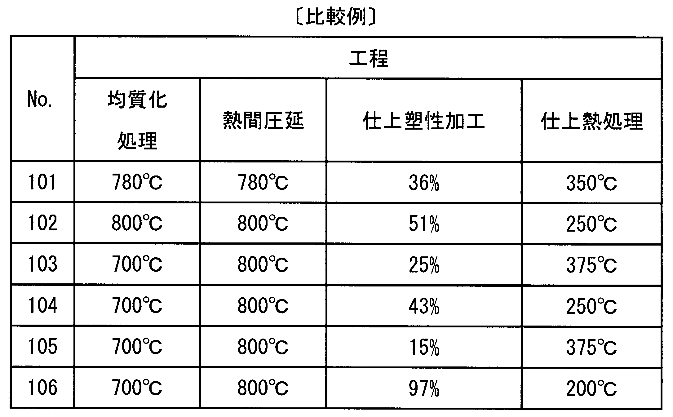
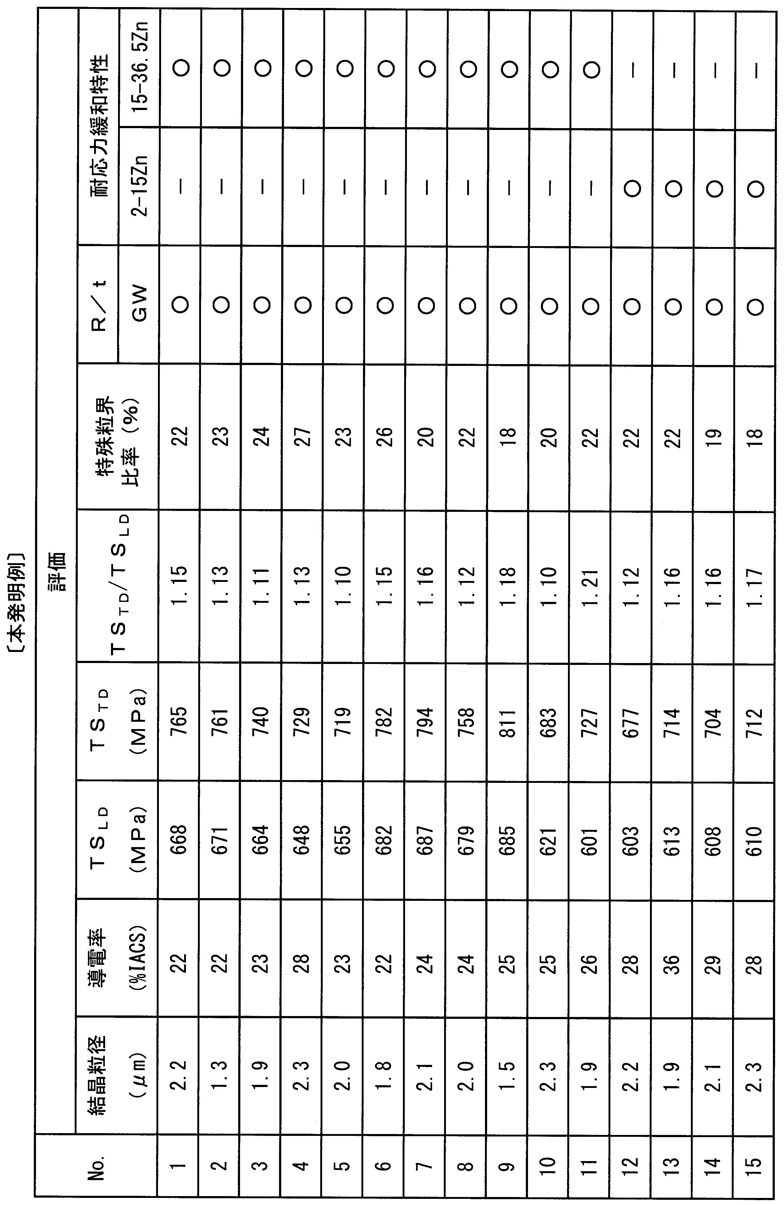


比較例102においては、Pが含有されておらず、Pの含有量が本発明の範囲外であり、耐応力緩和特性が「×」の評価となった。
比較例103においては、Ni、Pが添加されておらず、Ni、Pの含有量が本発明の範囲外であり、かつ、強度比TSTD/TSLDが1.09未満であり、圧延方向に対して直交になる方向に引張試験をしたときの引張強度TSTDが低くなった。また、耐応力緩和特性が「×」の評価となった。
比較例104においては、Snが添加されておらず、Snの含有量が本発明の範囲外であり、耐応力緩和特性が「×」の評価となった。
比較例105においては、Niが添加されておらず、Niの含有量が本発明の範囲外であり、かつ、強度比TSTD/TSLDが1.09未満であり、圧延方向に対して直交になる方向に引張試験をしたときの引張強度TSTDが低く、耐応力緩和特性が「×」の評価となった。
比較例106においては、強度比TSTD/TSLDが1.3を超えており、曲げ加工性が「×」の評価となった。このため、耐応力緩和試験は実施しなかった。
Claims (11)
- Znを2.0mass%超えて36.5mass%以下、Snを0.10mass%以上0.90mass%以下、Niを0.15mass%以上1.00mass%未満、Pを0.005mass%以上0.100mass%以下含有し、残部がCu及び不可避的不純物からなり、
Niの含有量とPの含有量との比Ni/Pが、原子比で、
3.00<Ni/P<100.00を満たし、
さらに、Snの含有量とNiの含有量との比Sn/Niが、原子比で、
0.10<Sn/Ni<2.90を満たすとともに、
圧延方向に対して直交方向に引張試験を行った際の強度TSTDと、圧延方向に対して平行方向に引張試験を行った際の強度TSLDと、から算出される強度比TSTD/TSLDが1.09を超えることを特徴する電子・電気機器用銅合金。 - Znを2.0mass%超えて36.5mass%以下、Snを0.10mass%以上0.90mass%以下、Niを0.15mass%以上1.00mass%未満、Pを0.005mass%以上0.100mass%以下含有するとともに、
0.001mass%以上0.100mass%未満のFe及び0.001mass%以上0.100mass%未満のCoのいずれか一方又は両方を含有し、残部がCuおよび不可避的不純物からなり、
Ni、FeおよびCoの合計含有量(Ni+Fe+Co)とPの含有量との比(Ni+Fe+Co)/Pが、原子比で、
3.00<(Ni+Fe+Co)/P<100.00を満たし、
かつSnの含有量とNi、FeおよびCoの合計含有量(Ni+Fe+Co)との比Sn/(Ni+Fe+Co)が、原子比で、
0.10<Sn/(Ni+Fe+Co)<2.90を満たし、
さらにFeとCoの合計含有量とNiの含有量との比(Fe+Co)/Niが、原子比で、
0.002≦(Fe+Co)/Ni<1.500を満たすとともに、
圧延方向に対して直交方向に引張試験を行った際の強度TSTDと、圧延方向に対して平行方向に引張試験を行った際の強度TSLDと、から算出される強度比TSTD/TSLDが1.09を超えることを特徴する電子・電気機器用銅合金。 - 圧延方向に対して直交方向に引張試験を行った際の強度TSTDが500MPa以上であり、圧延方向に対して直交する方向を曲げの軸としたとき、W曲げ冶具の半径をRとし、銅合金の厚みをtとしたときの比で表わされる曲げ加工性R/tが1以下であることを特徴とする請求項1または請求項2に記載の電子・電気機器用銅合金。
- Cu、ZnおよびSnを含有するα相の結晶粒の平均結晶粒径が0.1μm以上15μm以下の範囲内であり、FeとCoとNiからなる群から選択される少なくとも一種の元素とPとを含有する析出物が含まれていることを特徴とする請求項1から請求項3のいずれか一項に記載の電子・電気機器用銅合金。
- Cu、ZnおよびSnを含有するα相を、EBSD法により1000μm2以上の測定面積を測定間隔0.1μmステップで測定して、データ解析ソフトOIMにより解析されたCI値が0.1以下である測定点を除いて解析し、隣接する測定点間の方位差が15°を超える測定点間を結晶粒界とし、全ての結晶粒界長さLに対するΣ3、Σ9、Σ27a、Σ27bの各粒界長さの和Lσの比率である特殊粒界長さ比率(Lσ/L)が10%以上であることを特徴とする請求項1から請求項4のいずれか一項に記載の電子・電気機器用銅合金。
- 請求項1から請求項5のいずれか一項に記載の電子・電気機器用銅合金の圧延材からなり、厚みが0.05mm以上1.0mm以下の範囲内にあることを特徴とする電子・電気機器用銅合金薄板。
- 表面にSnめっきが施されていることを特徴とする請求項6に記載の電子・電気機器用銅合金薄板。
- 請求項1から請求項5のいずれか一項に記載の電子・電気機器用銅合金からなることを特徴とする電子・電気機器用導電部品。
- 請求項1から請求項5のいずれか一項に記載の電子・電気機器用銅合金からなることを特徴とする端子。
- 請求項6または請求項7に記載の電子・電気機器用銅合金薄板からなることを特徴とする電子・電気機器用導電部品。
- 請求項6または請求項7に記載の電子・電気機器用銅合金薄板からなることを特徴とする端子。
Priority Applications (6)
| Application Number | Priority Date | Filing Date | Title |
|---|---|---|---|
| JP2014530436A JP5690979B1 (ja) | 2013-07-10 | 2014-02-20 | 電子・電気機器用銅合金、電子・電気機器用銅合金薄板、電子・電気機器用導電部品及び端子 |
| EP14823795.1A EP3020838A4 (en) | 2013-07-10 | 2014-02-20 | Copper alloy for electronic and electrical equipment, copper alloy thin sheet for electronic and electrical equipment, and conductive component for electronic and electrical equipment, terminal |
| MX2016000027A MX2016000027A (es) | 2013-07-10 | 2014-02-20 | Aleacion de cobre para equipo electronico y electrico, hoja delgada de aleacion de cobre para equipo electronico y/o electrico, y componente conductor para equipo electronico y electrico y terminal. |
| KR1020157037093A KR20160029033A (ko) | 2013-07-10 | 2014-02-20 | 전자·전기 기기용 구리 합금, 전자·전기 기기용 구리 합금 박판, 전자·전기 기기용 도전 부품 및 단자 |
| CN201480032727.6A CN105339513B (zh) | 2013-07-10 | 2014-02-20 | 电子电气设备用铜合金、电子电气设备用铜合金薄板、电子电气设备用导电元件及端子 |
| US14/898,950 US10190194B2 (en) | 2013-07-10 | 2014-02-20 | Copper alloy for electronic and electrical equipment, copper alloy thin sheet for electronic and electrical equipment, and conductive component for electronic and electrical equipment, terminal |
Applications Claiming Priority (4)
| Application Number | Priority Date | Filing Date | Title |
|---|---|---|---|
| JP2013-145007 | 2013-07-10 | ||
| JP2013145007 | 2013-07-10 | ||
| JP2013273548 | 2013-12-27 | ||
| JP2013-273548 | 2013-12-27 |
Publications (1)
| Publication Number | Publication Date |
|---|---|
| WO2015004939A1 true WO2015004939A1 (ja) | 2015-01-15 |
Family
ID=52279639
Family Applications (1)
| Application Number | Title | Priority Date | Filing Date |
|---|---|---|---|
| PCT/JP2014/054042 Ceased WO2015004939A1 (ja) | 2013-07-10 | 2014-02-20 | 電子・電気機器用銅合金、電子・電気機器用銅合金薄板、電子・電気機器用導電部品及び端子 |
Country Status (8)
| Country | Link |
|---|---|
| US (1) | US10190194B2 (ja) |
| EP (1) | EP3020838A4 (ja) |
| JP (2) | JP5690979B1 (ja) |
| KR (1) | KR20160029033A (ja) |
| CN (1) | CN105339513B (ja) |
| MX (1) | MX2016000027A (ja) |
| TW (1) | TWI512122B (ja) |
| WO (1) | WO2015004939A1 (ja) |
Cited By (2)
| Publication number | Priority date | Publication date | Assignee | Title |
|---|---|---|---|---|
| JP2019173092A (ja) * | 2018-03-28 | 2019-10-10 | 三菱マテリアル株式会社 | 電子・電気機器用銅合金、電子・電気機器用銅合金薄板、電子・電気機器用導電部品及び端子 |
| JP2019173093A (ja) * | 2018-03-28 | 2019-10-10 | 三菱マテリアル株式会社 | 電子・電気機器用銅合金、電子・電気機器用銅合金薄板、電子・電気機器用導電部品及び端子 |
Families Citing this family (9)
| Publication number | Priority date | Publication date | Assignee | Title |
|---|---|---|---|---|
| JP6264887B2 (ja) * | 2013-07-10 | 2018-01-24 | 三菱マテリアル株式会社 | 電子・電気機器用銅合金、電子・電気機器用銅合金薄板、電子・電気機器用導電部品及び端子 |
| JP6464743B2 (ja) * | 2014-12-26 | 2019-02-06 | 三菱マテリアル株式会社 | 電子・電気機器用銅合金、電子・電気機器用銅合金薄板、電子・電気機器用部品、及び、端子 |
| JP6101750B2 (ja) * | 2015-07-30 | 2017-03-22 | 三菱マテリアル株式会社 | 電子・電気機器用銅合金、電子・電気機器用銅合金薄板、電子・電気機器用導電部品および端子 |
| CN114959230B (zh) * | 2017-02-04 | 2024-08-16 | 美题隆公司 | 铜镍锡合金带材或板材及其制备方法 |
| KR101900793B1 (ko) | 2017-06-08 | 2018-09-20 | 주식회사 풍산 | 전기·전자, 자동차 부품용 동합금의 주석 도금 방법 및 이로부터 제조된 동합금의 주석 도금재 |
| JP6648088B2 (ja) * | 2017-10-19 | 2020-02-14 | Jx金属株式会社 | 二次電池負極集電体用圧延銅箔、それを用いた二次電池負極及び二次電池並びに二次電池負極集電体用圧延銅箔の製造方法 |
| WO2021025071A1 (ja) * | 2019-08-06 | 2021-02-11 | 三菱マテリアル株式会社 | 銅合金板、めっき皮膜付銅合金板及びこれらの製造方法 |
| JP7014211B2 (ja) * | 2019-09-27 | 2022-02-01 | 三菱マテリアル株式会社 | 電子・電気機器用銅合金、電子・電気機器用銅合金板条材、電子・電気機器用部品、端子、及び、バスバー |
| CN117373728B (zh) * | 2022-06-30 | 2024-09-10 | 比亚迪股份有限公司 | 导电排、导电排组件及车用电气设备系统 |
Citations (9)
| Publication number | Priority date | Publication date | Assignee | Title |
|---|---|---|---|---|
| JPH0533087A (ja) | 1991-07-31 | 1993-02-09 | Furukawa Electric Co Ltd:The | 小型導電性部材用銅合金 |
| JP3717321B2 (ja) | 1998-12-11 | 2005-11-16 | 古河電気工業株式会社 | 半導体リードフレーム用銅合金 |
| JP2006283060A (ja) | 2005-03-31 | 2006-10-19 | Dowa Mining Co Ltd | 銅合金材料およびその製造法 |
| JP3953357B2 (ja) | 2002-04-17 | 2007-08-08 | 株式会社神戸製鋼所 | 電気、電子部品用銅合金 |
| JP5153949B1 (ja) * | 2012-03-30 | 2013-02-27 | Jx日鉱日石金属株式会社 | Cu−Zn−Sn−Ni−P系合金 |
| JP5303678B1 (ja) * | 2012-01-06 | 2013-10-02 | 三菱マテリアル株式会社 | 電子・電気機器用銅合金、電子・電気機器用銅合金薄板、電子・電気機器用導電部品および端子 |
| JP2013213236A (ja) * | 2012-03-30 | 2013-10-17 | Jx Nippon Mining & Metals Corp | Cu−Zn−Sn−Ni−P系合金 |
| JP5417539B1 (ja) * | 2013-01-28 | 2014-02-19 | 三菱マテリアル株式会社 | 電子・電気機器用銅合金、電子・電気機器用銅合金薄板、電子・電気機器用導電部品及び端子 |
| JP5417523B1 (ja) * | 2012-12-28 | 2014-02-19 | 三菱マテリアル株式会社 | 電子・電気機器用銅合金、電子・電気機器用銅合金薄板、電子・電気機器用導電部品及び端子 |
Family Cites Families (9)
| Publication number | Priority date | Publication date | Assignee | Title |
|---|---|---|---|---|
| US6471792B1 (en) * | 1998-11-16 | 2002-10-29 | Olin Corporation | Stress relaxation resistant brass |
| JP2005060773A (ja) | 2003-08-12 | 2005-03-10 | Mitsui Mining & Smelting Co Ltd | 特殊黄銅及びその特殊黄銅の高力化方法 |
| CN101693960B (zh) | 2005-06-08 | 2011-09-07 | 株式会社神户制钢所 | 铜合金、铜合金板及其制造方法 |
| JP4157898B2 (ja) | 2006-10-02 | 2008-10-01 | 株式会社神戸製鋼所 | プレス打ち抜き性に優れた電気電子部品用銅合金板 |
| JP5150908B2 (ja) | 2008-07-07 | 2013-02-27 | Dowaメタルテック株式会社 | コネクタ用銅合金とその製造法 |
| JP5088425B2 (ja) * | 2011-01-13 | 2012-12-05 | 三菱マテリアル株式会社 | 電子・電気機器用銅合金、銅合金薄板および導電部材 |
| CN103748244B (zh) * | 2011-09-16 | 2015-04-22 | 三菱伸铜株式会社 | 铜合金板及铜合金板的制造方法 |
| MX2013015230A (es) * | 2011-09-16 | 2014-02-19 | Mitsubishi Shindo Kk | Lamina de aleacion de cobre y metodo para producir lamina de aleacion de cobre. |
| KR101476592B1 (ko) | 2011-09-20 | 2014-12-24 | 미쓰비시 신도 가부시키가이샤 | 구리 합금판 및 구리 합금판의 제조방법 |
-
2014
- 2014-02-20 JP JP2014530436A patent/JP5690979B1/ja not_active Expired - Fee Related
- 2014-02-20 WO PCT/JP2014/054042 patent/WO2015004939A1/ja not_active Ceased
- 2014-02-20 KR KR1020157037093A patent/KR20160029033A/ko not_active Withdrawn
- 2014-02-20 TW TW103105645A patent/TWI512122B/zh active
- 2014-02-20 US US14/898,950 patent/US10190194B2/en active Active
- 2014-02-20 MX MX2016000027A patent/MX2016000027A/es unknown
- 2014-02-20 CN CN201480032727.6A patent/CN105339513B/zh active Active
- 2014-02-20 EP EP14823795.1A patent/EP3020838A4/en not_active Withdrawn
- 2014-11-07 JP JP2014227338A patent/JP2015143386A/ja active Pending
Patent Citations (9)
| Publication number | Priority date | Publication date | Assignee | Title |
|---|---|---|---|---|
| JPH0533087A (ja) | 1991-07-31 | 1993-02-09 | Furukawa Electric Co Ltd:The | 小型導電性部材用銅合金 |
| JP3717321B2 (ja) | 1998-12-11 | 2005-11-16 | 古河電気工業株式会社 | 半導体リードフレーム用銅合金 |
| JP3953357B2 (ja) | 2002-04-17 | 2007-08-08 | 株式会社神戸製鋼所 | 電気、電子部品用銅合金 |
| JP2006283060A (ja) | 2005-03-31 | 2006-10-19 | Dowa Mining Co Ltd | 銅合金材料およびその製造法 |
| JP5303678B1 (ja) * | 2012-01-06 | 2013-10-02 | 三菱マテリアル株式会社 | 電子・電気機器用銅合金、電子・電気機器用銅合金薄板、電子・電気機器用導電部品および端子 |
| JP5153949B1 (ja) * | 2012-03-30 | 2013-02-27 | Jx日鉱日石金属株式会社 | Cu−Zn−Sn−Ni−P系合金 |
| JP2013213236A (ja) * | 2012-03-30 | 2013-10-17 | Jx Nippon Mining & Metals Corp | Cu−Zn−Sn−Ni−P系合金 |
| JP5417523B1 (ja) * | 2012-12-28 | 2014-02-19 | 三菱マテリアル株式会社 | 電子・電気機器用銅合金、電子・電気機器用銅合金薄板、電子・電気機器用導電部品及び端子 |
| JP5417539B1 (ja) * | 2013-01-28 | 2014-02-19 | 三菱マテリアル株式会社 | 電子・電気機器用銅合金、電子・電気機器用銅合金薄板、電子・電気機器用導電部品及び端子 |
Non-Patent Citations (4)
| Title |
|---|
| D. G BRANDON, ACTA. METALLURGICA, vol. 14, 1966, pages 1479 |
| KRONBERG ET AL., TRANS. MET. SOC. AIME, vol. 185, 1949, pages 501 |
| See also references of EP3020838A4 * |
| SEIICHI SUZUKI: "EBSD : using OIM (third edition)", 2009, TSL SOLUTION PUBLICATION, pages: 9 |
Cited By (4)
| Publication number | Priority date | Publication date | Assignee | Title |
|---|---|---|---|---|
| JP2019173092A (ja) * | 2018-03-28 | 2019-10-10 | 三菱マテリアル株式会社 | 電子・電気機器用銅合金、電子・電気機器用銅合金薄板、電子・電気機器用導電部品及び端子 |
| JP2019173093A (ja) * | 2018-03-28 | 2019-10-10 | 三菱マテリアル株式会社 | 電子・電気機器用銅合金、電子・電気機器用銅合金薄板、電子・電気機器用導電部品及び端子 |
| JP7172090B2 (ja) | 2018-03-28 | 2022-11-16 | 三菱マテリアル株式会社 | 電子・電気機器用銅合金、電子・電気機器用銅合金薄板、電子・電気機器用導電部品及び端子 |
| JP7172089B2 (ja) | 2018-03-28 | 2022-11-16 | 三菱マテリアル株式会社 | 電子・電気機器用銅合金、電子・電気機器用銅合金薄板、電子・電気機器用導電部品及び端子 |
Also Published As
| Publication number | Publication date |
|---|---|
| EP3020838A1 (en) | 2016-05-18 |
| TW201504461A (zh) | 2015-02-01 |
| EP3020838A4 (en) | 2017-04-19 |
| JP2015143386A (ja) | 2015-08-06 |
| MX2016000027A (es) | 2016-10-31 |
| TWI512122B (zh) | 2015-12-11 |
| CN105339513A (zh) | 2016-02-17 |
| KR20160029033A (ko) | 2016-03-14 |
| JPWO2015004939A1 (ja) | 2017-03-02 |
| CN105339513B (zh) | 2017-06-09 |
| US20160369374A1 (en) | 2016-12-22 |
| JP5690979B1 (ja) | 2015-03-25 |
| US10190194B2 (en) | 2019-01-29 |
Similar Documents
| Publication | Publication Date | Title |
|---|---|---|
| JP5690979B1 (ja) | 電子・電気機器用銅合金、電子・電気機器用銅合金薄板、電子・電気機器用導電部品及び端子 | |
| JP5303678B1 (ja) | 電子・電気機器用銅合金、電子・電気機器用銅合金薄板、電子・電気機器用導電部品および端子 | |
| JP5572754B2 (ja) | 電子・電気機器用銅合金、電子・電気機器用銅合金薄板、電子・電気機器用導電部品及び端子 | |
| JP5417523B1 (ja) | 電子・電気機器用銅合金、電子・電気機器用銅合金薄板、電子・電気機器用導電部品及び端子 | |
| JP5604549B2 (ja) | 電子・電気機器用銅合金、電子・電気機器用銅合金薄板、電子・電気機器用導電部品及び端子 | |
| JP5417539B1 (ja) | 電子・電気機器用銅合金、電子・電気機器用銅合金薄板、電子・電気機器用導電部品及び端子 | |
| JP5957083B2 (ja) | 電子・電気機器用銅合金、電子・電気機器用銅合金薄板、電子・電気機器用導電部品及び端子 | |
| JP2014148748A (ja) | 電子・電気機器用銅合金、電子・電気機器用銅合金薄板、電子・電気機器用銅合金の製造方法、電子・電気機器用導電部品および端子 | |
| JP5501495B1 (ja) | 電子・電気機器用銅合金、電子・電気機器用銅合金薄板、電子・電気機器用導電部品及び端子 | |
| JP5572753B2 (ja) | 電子・電気機器用銅合金、電子・電気機器用銅合金薄板、電子・電気機器用導電部品及び端子 | |
| JP2016132816A (ja) | 電子・電気機器用銅合金、電子・電気機器用銅合金薄板、電子・電気機器用導電部品及び端子 | |
| JP2014118595A (ja) | 電子・電気機器用銅合金、電子・電気機器用銅合金薄板、電子・電気機器用導電部品及び端子 | |
| JP6264887B2 (ja) | 電子・電気機器用銅合金、電子・電気機器用銅合金薄板、電子・電気機器用導電部品及び端子 | |
| JP6097575B2 (ja) | 電子・電気機器用銅合金、電子・電気機器用銅合金薄板、電子・電気機器用導電部品及び端子 | |
| JP6304864B2 (ja) | 電子・電気機器用銅合金、電子・電気機器用銅合金薄板、電子・電気機器用導電部品及び端子 | |
| JP6097606B2 (ja) | 電子・電気機器用銅合金、電子・電気機器用銅合金薄板、電子・電気機器用導電部品及び端子 | |
| JP6304867B2 (ja) | 電子・電気機器用銅合金、電子・電気機器用銅合金薄板、電子・電気機器用導電部品及び端子 | |
| JP6304865B2 (ja) | 電子・電気機器用銅合金、電子・電気機器用銅合金薄板、電子・電気機器用導電部品及び端子 | |
| JP6097576B2 (ja) | 電子・電気機器用銅合金、電子・電気機器用銅合金薄板、電子・電気機器用導電部品及び端子 | |
| JP6304863B2 (ja) | 電子・電気機器用銅合金、電子・電気機器用銅合金薄板、電子・電気機器用導電部品及び端子 | |
| JP2019173093A (ja) | 電子・電気機器用銅合金、電子・電気機器用銅合金薄板、電子・電気機器用導電部品及び端子 | |
| JP2019173092A (ja) | 電子・電気機器用銅合金、電子・電気機器用銅合金薄板、電子・電気機器用導電部品及び端子 |
Legal Events
| Date | Code | Title | Description |
|---|---|---|---|
| WWE | Wipo information: entry into national phase |
Ref document number: 201480032727.6 Country of ref document: CN |
|
| ENP | Entry into the national phase |
Ref document number: 2014530436 Country of ref document: JP Kind code of ref document: A |
|
| 121 | Ep: the epo has been informed by wipo that ep was designated in this application |
Ref document number: 14823795 Country of ref document: EP Kind code of ref document: A1 |
|
| WWE | Wipo information: entry into national phase |
Ref document number: 14898950 Country of ref document: US |
|
| WWE | Wipo information: entry into national phase |
Ref document number: 2014823795 Country of ref document: EP |
|
| ENP | Entry into the national phase |
Ref document number: 20157037093 Country of ref document: KR Kind code of ref document: A |
|
| WWE | Wipo information: entry into national phase |
Ref document number: MX/A/2016/000027 Country of ref document: MX |
|
| NENP | Non-entry into the national phase |
Ref country code: DE |