WO2015015578A1 - 電子部品装着装置及び装着方法 - Google Patents
電子部品装着装置及び装着方法 Download PDFInfo
- Publication number
- WO2015015578A1 WO2015015578A1 PCT/JP2013/070679 JP2013070679W WO2015015578A1 WO 2015015578 A1 WO2015015578 A1 WO 2015015578A1 JP 2013070679 W JP2013070679 W JP 2013070679W WO 2015015578 A1 WO2015015578 A1 WO 2015015578A1
- Authority
- WO
- WIPO (PCT)
- Prior art keywords
- electronic component
- substrate
- mounting
- component
- cover
- Prior art date
- Legal status (The legal status is an assumption and is not a legal conclusion. Google has not performed a legal analysis and makes no representation as to the accuracy of the status listed.)
- Ceased
Links
Images



Classifications
-
- H—ELECTRICITY
- H05—ELECTRIC TECHNIQUES NOT OTHERWISE PROVIDED FOR
- H05K—PRINTED CIRCUITS; CASINGS OR CONSTRUCTIONAL DETAILS OF ELECTRIC APPARATUS; MANUFACTURE OF ASSEMBLAGES OF ELECTRICAL COMPONENTS
- H05K13/00—Apparatus or processes specially adapted for manufacturing or adjusting assemblages of electric components
- H05K13/04—Mounting of components, e.g. of leadless components
- H05K13/0404—Pick-and-place heads or apparatus, e.g. with jaws
-
- H—ELECTRICITY
- H05—ELECTRIC TECHNIQUES NOT OTHERWISE PROVIDED FOR
- H05K—PRINTED CIRCUITS; CASINGS OR CONSTRUCTIONAL DETAILS OF ELECTRIC APPARATUS; MANUFACTURE OF ASSEMBLAGES OF ELECTRICAL COMPONENTS
- H05K13/00—Apparatus or processes specially adapted for manufacturing or adjusting assemblages of electric components
- H05K13/04—Mounting of components, e.g. of leadless components
- H05K13/046—Surface mounting
-
- H—ELECTRICITY
- H05—ELECTRIC TECHNIQUES NOT OTHERWISE PROVIDED FOR
- H05K—PRINTED CIRCUITS; CASINGS OR CONSTRUCTIONAL DETAILS OF ELECTRIC APPARATUS; MANUFACTURE OF ASSEMBLAGES OF ELECTRICAL COMPONENTS
- H05K13/00—Apparatus or processes specially adapted for manufacturing or adjusting assemblages of electric components
- H05K13/08—Monitoring manufacture of assemblages
-
- H—ELECTRICITY
- H05—ELECTRIC TECHNIQUES NOT OTHERWISE PROVIDED FOR
- H05K—PRINTED CIRCUITS; CASINGS OR CONSTRUCTIONAL DETAILS OF ELECTRIC APPARATUS; MANUFACTURE OF ASSEMBLAGES OF ELECTRICAL COMPONENTS
- H05K9/00—Screening of apparatus or components against electric or magnetic fields
- H05K9/0007—Casings
- H05K9/002—Casings with localised screening
- H05K9/0022—Casings with localised screening of components mounted on printed circuit boards [PCB]
- H05K9/0024—Shield cases mounted on a PCB, e.g. cans or caps or conformal shields
- H05K9/0032—Shield cases mounted on a PCB, e.g. cans or caps or conformal shields having multiple parts, e.g. frames mating with lids
-
- H—ELECTRICITY
- H05—ELECTRIC TECHNIQUES NOT OTHERWISE PROVIDED FOR
- H05K—PRINTED CIRCUITS; CASINGS OR CONSTRUCTIONAL DETAILS OF ELECTRIC APPARATUS; MANUFACTURE OF ASSEMBLAGES OF ELECTRICAL COMPONENTS
- H05K9/00—Screening of apparatus or components against electric or magnetic fields
- H05K9/0007—Casings
- H05K9/002—Casings with localised screening
- H05K9/0022—Casings with localised screening of components mounted on printed circuit boards [PCB]
- H05K9/0024—Shield cases mounted on a PCB, e.g. cans or caps or conformal shields
- H05K9/0032—Shield cases mounted on a PCB, e.g. cans or caps or conformal shields having multiple parts, e.g. frames mating with lids
- H05K9/0035—Shield cases mounted on a PCB, e.g. cans or caps or conformal shields having multiple parts, e.g. frames mating with lids with retainers mounted beforehand on the PCB, e.g. clips
-
- Y—GENERAL TAGGING OF NEW TECHNOLOGICAL DEVELOPMENTS; GENERAL TAGGING OF CROSS-SECTIONAL TECHNOLOGIES SPANNING OVER SEVERAL SECTIONS OF THE IPC; TECHNICAL SUBJECTS COVERED BY FORMER USPC CROSS-REFERENCE ART COLLECTIONS [XRACs] AND DIGESTS
- Y10—TECHNICAL SUBJECTS COVERED BY FORMER USPC
- Y10T—TECHNICAL SUBJECTS COVERED BY FORMER US CLASSIFICATION
- Y10T29/00—Metal working
- Y10T29/53—Means to assemble or disassemble
- Y10T29/5313—Means to assemble electrical device
- Y10T29/53174—Means to fasten electrical component to wiring board, base, or substrate
-
- Y—GENERAL TAGGING OF NEW TECHNOLOGICAL DEVELOPMENTS; GENERAL TAGGING OF CROSS-SECTIONAL TECHNOLOGIES SPANNING OVER SEVERAL SECTIONS OF THE IPC; TECHNICAL SUBJECTS COVERED BY FORMER USPC CROSS-REFERENCE ART COLLECTIONS [XRACs] AND DIGESTS
- Y10—TECHNICAL SUBJECTS COVERED BY FORMER USPC
- Y10T—TECHNICAL SUBJECTS COVERED BY FORMER US CLASSIFICATION
- Y10T29/00—Metal working
- Y10T29/53—Means to assemble or disassemble
- Y10T29/5313—Means to assemble electrical device
- Y10T29/53252—Means to simultaneously fasten three or more parts
Definitions
- the present invention relates to an electronic component mounting apparatus that presses a cover component that covers an electronic component mounted on a substrate and attaches the cover component to the substrate, and a mounting method thereof.
- Patent Document 1 describes an electronic component mounting method in which one cover component is positioned and placed on a substrate with respect to one frame member.
- one frame member is standingly arranged so that the electronic component covered with a board
- substrate may be enclosed.
- a mounting device including a large nozzle or chuck capable of collecting the frame member is required. This becomes a problem in an electronic component mounting apparatus that attempts to save space together with efficiency.
- the present invention has been made in view of the related problems, and a clip and a cover component can be mounted / placed by an electronic component mounting apparatus using a clip instead of the frame member of Patent Document 1.
- An electronic component mounting apparatus and method are provided.
- the structural feature of the invention according to claim 1 is that a substrate transport device that transports and positions a substrate on which an electronic component is mounted, and positions the electronic component at a mounting position of the substrate.
- a mounting device to be mounted a mounting device that collects a plurality of engaged portions and positions and mounts them on the mounting position of the substrate, and an engaging portion at a predetermined position that covers the mounted electronic component.
- a mounting device that collects the provided cover parts and positions and places the engaging portion at the position of the corresponding engaged portion.
- the present invention can provide an efficient and space-saving electronic component mounting apparatus and method.
- the top view which shows the outline of the electronic component mounting apparatus which concerns on this embodiment.
- the flowchart which shows the procedure which attaches a cover component to a board
- the electronic component mounting apparatus 2 includes a substrate transfer device 4 that loads a substrate 3 into a loading position and positions the substrate 3 at a predetermined position, a component supply device 5, and a base 6 in a horizontal direction.
- a component transfer device 12 and a mark recognition camera 14 having a mounting head 10 provided on a movable table 8 supported so as to be movable in a certain X direction and Y direction, and a component recognition camera 16 fixed to the base 6.
- a control device 18 for controlling the mounting by the component transfer device 12.
- the substrate transfer device 4 is a so-called double conveyor type, and each conveyor is provided in parallel along a guide rail 20 extending in the X direction and is provided in parallel with a conveyor belt (in parallel) for carrying the substrate 3 to a positioned position. (Not shown), a support frame (not shown) for supporting each of the loaded substrates 3, and a lifting device (not shown) for raising the supported substrates 3 to a mounting position (predetermined position). And a clamping device (not shown) for clamping the substrate 3 at each position (mounting position).
- a support frame not shown
- a lifting device for raising the supported substrates 3 to a mounting position (predetermined position).
- a clamping device (not shown) for clamping the substrate 3 at each position (mounting position).
- the component supply device 5 is configured by arranging a plurality of cassette-type feeders 21 in parallel on the side portion (front side in FIG. 1) of the substrate transfer device 4.
- Each of the cassette type feeders 21 includes a case part detachably attached to the slot (not shown), a supply reel provided at the rear part of the case part, and a component take-out part provided at the tip of the case part.
- a long and narrow tape (not shown) in which electronic components 40 (see FIG. 6) are sealed at a predetermined pitch is wound and held on the supply reel, and this tape is pulled out at a predetermined pitch by a sprocket (not shown). Is released from the encapsulated state and sequentially fed into the component take-out section.
- a code (identification code) is affixed to the cassette-type feeder 21, and correspondence data between the code and the ID, part number, number of enclosures, part weight, etc. of the electronic part 40 is a host that manages the entire line in the control device 18. It is recorded in advance in mounting program data transmitted from a computer (not shown).
- a component tray 17 is disposed on a side portion (upper side in FIG. 1) of the substrate transport device 4, and a large electronic component and a cover component 19 are accommodated in the component tray 17. Further, the clip 100 is also supplied in the same manner as the electronic component 40. *
- An X-direction moving beam 22 is provided above the substrate transport device 4, and the X-direction moving beam 22 extends in the Y direction and extends in the X direction along the substrate transport device 4 ( It is provided so as to be movable along (not shown).
- the moving table 8 is provided on the X direction moving beam 22 so as to be movable on a Y direction rail (not shown) provided on the side surface of the X direction moving beam 22 via a slider (not shown). It has been.
- the moving table 8 holds a component transfer device 12 having a mounting head 10 and a mark recognition camera 14 so as to be movable together with the moving table 8.
- the X-direction moving beam 22 is driven by a servo motor via a ball screw mechanism (not shown), and the moving table 8 is driven by a servo motor (not shown) via a Y-direction moving ball screw mechanism (not shown). .
- the drive of these servo motors is controlled by the control device 18.
- the optical axis of the mark recognition camera 14 is parallel to the Z direction perpendicular to the X direction and the Y direction.
- a captured image captured by the mark recognition camera 14 is input to an unillustrated image recognition apparatus including an unillustrated A / D converter.
- the image recognition apparatus captures the captured image and reads information from the reference mark m (see FIG. 6). Then, the positional deviation of the reference mark m is calculated by a calculation device (not shown) provided in the control device 18. Next, when the mark recognition camera 14 is moved, the position deviation is corrected and moved. *
- the component transfer device 12 includes the moving table 8, a mounting head lifting device (not shown) supported by the moving table 8 so as to be movable up and down in the Z direction perpendicular to the X direction and the Y direction, and the mounting head lifting device.
- the mounting head 10 is supported. As shown in FIG. 2, the mounting head 10 is provided with a pair of nozzle holders 24, 26, and each nozzle holder 24, 26 is supported by a bearing (not shown) so as to be rotatable in the axial direction.
- the nozzle holders 24 and 26 are supported by a guide member (not shown) so as to be movable up and down.
- the nozzle holders 24 and 26 are vertically driven by a nozzle holder lifting device (not shown) driven by a servo motor (not shown).
- the nozzle holders 24 and 26 are rotationally driven around their central axes by a rotation driving mechanism (not shown) and a servo motor (not shown) that drives the rotation driving mechanism. *
- axial suction nozzles 28 and 30 are removably fitted.
- one of the suction nozzles 28 and 30 is formed with a rectangular pressing portion 32 at the lower end.
- a negative pressure passage 36 communicating with a negative pressure supply pump 34 that is a negative pressure source is opened at the lower end of the pressing portion 32.
- An electromagnetic valve 38 is provided between the negative pressure flow path 36 and the negative pressure supply pump 34, and the negative pressure air from the negative pressure supply pump 34 to the negative pressure flow path 36 can be communicated and blocked by the electromagnetic valve 38. .
- the operation of the electromagnetic valve 38 is controlled by the control device 18.
- the tip of the suction nozzle 28 and the opening of the negative pressure flow path 36 of the suction nozzle 30 are adapted to suck and hold the electronic component 40 and the like by supplying negative pressure air.
- the nozzle holders 24 and 26 and the suction nozzles 28 and 30 constitute a vertically moving member.
- a component recognition camera 16 is provided between the substrate transfer device 4 and the component supply device 5, and the electronic component 40 sucked by the suction nozzles 28 and 30 is imaged by the component recognition camera 16 to produce the product. It is determined whether the electronic component is of a type suitable for the type of substrate to be printed, whether the suction state is good, and whether there is a defective portion of the component itself. The same applies to the clip 100 and the cover part 19. *
- the electronic component mounting apparatus 2 is provided with an input device 42 such as a keyboard for inputting board data, component data, and the like.
- the input device 42 is provided with a display device 44, and on the screen of the display device 44, substrate data, component data, calculation data, an image captured by the mark recognition camera 14 and the like can be displayed.
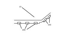
- the clip 100 used in the present embodiment is made of a metal such as a copper alloy or an aluminum alloy, for example, and as shown in FIGS. 3 and 4, the cover part opening 101, the cover part holding part 102, the board mounting surface. 103 is formed. *
- the cover component 19 used in the present embodiment is made of a metal such as a copper alloy or an aluminum alloy, and has a substantially rectangular plate shape as shown in FIGS. 5 and 8, and the engaging portion is folded at the peripheral edge. It is formed by bending and corresponds to the clip 100. *
- control device 18 carries the substrate 3 into the electronic component mounting device 2 and conveys it to the predetermined conveyance position by the substrate conveyance device 4 (S101).
- the substrate 3 transported to the predetermined transport position is raised from the predetermined transport position to the mounting position by a lifting device (not shown), positioned, and clamped by a clamping device (not shown) (substrate transport positioning step S102).
- the control device 18 positions the mark recognition camera 14 at a pair of reference marks m provided at the corners on the diagonal line of the positioned substrate 3, and the position coordinates of the reference mark m. Is read (S103). Thereby, in comparison with the position coordinate data of the substrate 3 stored in the storage device of the control device 18 in advance, the horizontal displacement (X direction, Y direction) of the position where the substrate 3 is positioned by the substrate transfer device 4. Direction and direction of rotation). *
- control device 18 collects the electronic component 40 from the cassette type feeder 21 by the suction nozzle 28 and positions and mounts the electronic component 40 on the position coordinate corrected on the substrate 3. Further, the clip 100 is sampled from the cassette type feeder 21 by the suction nozzle 28, and is positioned and mounted on the position coordinate corrected on the substrate 3 (component mounting / clip mounting step S104). Usually, the order of mounting and mounting the electronic component 40 and the clip 100 is determined by efficiency. *
- the control device 18 mounts at least the electronic component scheduled to be covered by the cover component 19 and mounts the clip 100 to be engaged with the cover component 19.
- the cover component 19 is collected from the suction nozzle 30 and positioned and placed at the position corrected position coordinates on the substrate 3. (Cover component placement step S105). *
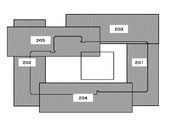
- the control device 18 raises the suction nozzle 30 above the cover component 19 and lowers the suction nozzle 30, thereby shortening the cover component 19 positioned below the pressing portion 201.
- One of the engaging portions facing in the hand direction is pressed (pressing first half step S106).
- the shape of the suction nozzle 30 may be any size as long as it can cover all of one of the engaging portions facing in the lateral direction. With such a size, it is possible to prevent the cover component 19 from being disengaged.
- the control device 18 moves the suction nozzle 30 up and then moves it, and lowers the suction nozzle 30, so that the other short part of the cover part 19 positioned below the pressing portion 202 is moved.
- the engaging part which opposes a hand direction is pressed (pressing first half process and S106). Thereafter, as shown in FIG. 9, the control device 18 controls the suction nozzle 30 in the order of the pressing portions 201, 202, 203, 204, 205 so as to press all of the plurality of engaging portions of the cover component 19. .
- control device 18 unclamps the substrate 3 to which the cover component 19 is assembled and lowers the substrate 3 from the mounting position to the transport position by the lifting device, and transfers it to the substrate transport device 4 (S109). *
- control apparatus 18 drives the board
- the mark recognition camera 14 measures the positions of at least two clips 100, stores the positions, and corrects the positioning.
- the cover component opening 101 is opened in the longitudinal direction, that is, the clip longitudinal direction without hatching in the drawing It is useful to select and use part or all of the positioning reference group 110.
- the cover component opening 101 is open in the short direction, that is, the clip short side that is hatched in the drawing. It is useful to select and use part or all of the directional positioning reference group 112. That is, in the cover component 19, the positioning correction to the planned placement position is performed by the clip longitudinal direction positioning reference group 110 and the clip short direction positioning reference group 112. This step is performed before S105.
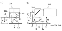
- the laser height sensor 306 has a laser light irradiation unit 361 and a reflected light detection unit 362 arranged adjacent to each other.
- the laser beam irradiation unit 361 irradiates the laser beam L1 downward toward the substrate K that is an object disposed below.
- the laser light L1 is reflected by the upper surface of the substrate K, and the reflected laser light L2 enters the reflected light detection unit 362.
- the reflected light detection unit 362 detects the height H of the object from the difference in the detection position of the reflected laser light L2.
- the reflected laser light L2 when the substrate K is at the normal height H and the reflected laser light L3 when the substrate Kx is at the height H3 above the normal are illustrated. Yes.
- the height measurement object of the laser height sensor 306 is the upper surface of the substrate K, and the height measurement is performed at a plurality of measurement positions.
- three measurement positions y1, y2, and y3 in the Y-axis direction of the substrate K are illustrated.
- height measurement is performed with a total of nine lattice points on the substrate K as measurement positions in consideration of three positions in the X-axis direction.
- the substrate K is a flat plate and maintains a horizontal posture, the same height H is measured at all measurement positions.
- different heights h1 to h3 are measured at each measurement position on the warped substrate Kx.
- the height of at least one place on the upper surface of the cover part 19 is measured, the height is stored in a storage device (not shown), and it is confirmed by a determination device (not shown) whether it is lower than a predetermined value.
- a determination device not shown
- the heights of at least three places on the upper surface may be measured.
- this step is considered to be performed after S108, but may be performed between S106 and S108.
- one of the two vertically moving members is the suction nozzle 28 and one is the suction nozzle 30.
- the number of vertically moving members is not limited to two, and may be one or three or more, for example.
- one electronic component mounting apparatus 2 is assumed, but a plurality of electronic component mounting apparatuses 2 may be used. *
- the height of the upper surface of the cover component 19 is measured by the height measuring function of the substrate camera 346, but the height may be measured by a laser or a contactor.
- the specific configuration described in the above-described embodiment is merely an example of the present invention, and the present invention is not limited to such a specific configuration. Various embodiments can be adopted without departing from the scope.
Landscapes
- Engineering & Computer Science (AREA)
- Microelectronics & Electronic Packaging (AREA)
- Manufacturing & Machinery (AREA)
- Operations Research (AREA)
- Supply And Installment Of Electrical Components (AREA)
Abstract
Description
い。このような大きさであれば、カバー部品19が未係合になることを防止することができる。次に、制御装置18は、図9に示すように、吸着ノズル30を上昇後、移動させ、吸着ノズル30を下降させることで、押圧部202の下に位置するカバー部品19のもう一方の短手方向に対向する係合部を押圧する(押圧前期工程・S106)。この後、制御装置18は、図9に示すように、カバー部品19について複数の係合部の全てを押圧するように押圧部201、202、203、204、205の順に吸着ノズル30を制御する。
Claims (8)
- 電子部品を装着する基板を搬送して位置決めする基板搬送装置と、前記電子部品を前記基板の装着位置に位置決めして装着する装着装置と、複数の被係合部を採取して前記基板の搭載位置に位置決めして搭載する搭載装置と、装着された前記電子部品をカバーする所定の位置に係合部を設けたカバー部品を採取して該係合部を対応する前記被係合部の位置に位置決めして載置する載置装置、とを備えていることを特徴とする電子部品装着装置。
- 請求項1に記載の電子部品装着装置は、前記カバー部品を押圧する押圧部を有する上下動装置と、前記上下動装置を駆動させて前記カバー部品を前記押圧部で複数回押圧する制御装置と、を有することを特徴とする電子部品装着装置。
- 請求項2に記載の制御装置は、前記カバー部品について複数の係合部の全てを押圧すること、を特徴とする電子部品装着装置。
- 請求項2に記載の制御装置は、前記カバー部品の4角でない角部を含む部分を複数回押圧のうち後半に押圧すること、を特徴とする電子部品装着装置。
- 請求項2乃至請求項4において、前記押圧部は前記電子部品を採取するノズルに設けられ、該ノズルは下端面に押圧用の平面を有することを特徴とする電子部品装着装置。
- 請求項2乃至請求項5において、前記電子部品装着装置は前記基板の高さを測定する測定装置を有し、該測定装置により前記カバー部品の高さの測定結果を記憶する高さ記憶装置と、該測定結果により押圧の良否を判定する判定装置を有することを特徴とする電子部品装着装置。
- 請求項1乃至請求項6において、前記基板に搭載された前記複数の被係合部から少なくとも2つ以上の被係合部を選択する選択装置と、選択された被係合部の搭載位置を計測する計測装置と、計測結果を記憶する位置記憶装置と、該計測結果により前記カバー部品の載置位置を補正すること補正装置、とを有することを特徴とする電子部品装着装置。
- 電子部品を装着する基板を搬送して位置決めし、前記電子部品を前記基板の装着位置に位置決めして装着し、複数の被係合部を採取して前記基板の搭載位置に位置決めして搭載し、装着された前記電子部品をカバーする所定の位置に係合部を設けたカバー部品を採取して該係合部を対応する前記被係合部の位置に位置決めして載置することを特徴とする電子部品装着方法。
Priority Applications (5)
| Application Number | Priority Date | Filing Date | Title |
|---|---|---|---|
| PCT/JP2013/070679 WO2015015578A1 (ja) | 2013-07-31 | 2013-07-31 | 電子部品装着装置及び装着方法 |
| CN201380078172.4A CN105379447B (zh) | 2013-07-31 | 2013-07-31 | 电子元件安装装置及安装方法 |
| JP2015529260A JP6346610B2 (ja) | 2013-07-31 | 2013-07-31 | 電子部品装着装置及び装着方法 |
| EP13890685.4A EP3030067B1 (en) | 2013-07-31 | 2013-07-31 | Electronic component mounting device and mounting method |
| US14/908,438 US10231370B2 (en) | 2013-07-31 | 2013-07-31 | Electronic component mounting device |
Applications Claiming Priority (1)
| Application Number | Priority Date | Filing Date | Title |
|---|---|---|---|
| PCT/JP2013/070679 WO2015015578A1 (ja) | 2013-07-31 | 2013-07-31 | 電子部品装着装置及び装着方法 |
Publications (1)
| Publication Number | Publication Date |
|---|---|
| WO2015015578A1 true WO2015015578A1 (ja) | 2015-02-05 |
Family
ID=52431158
Family Applications (1)
| Application Number | Title | Priority Date | Filing Date |
|---|---|---|---|
| PCT/JP2013/070679 Ceased WO2015015578A1 (ja) | 2013-07-31 | 2013-07-31 | 電子部品装着装置及び装着方法 |
Country Status (5)
| Country | Link |
|---|---|
| US (1) | US10231370B2 (ja) |
| EP (1) | EP3030067B1 (ja) |
| JP (1) | JP6346610B2 (ja) |
| CN (1) | CN105379447B (ja) |
| WO (1) | WO2015015578A1 (ja) |
Cited By (1)
| Publication number | Priority date | Publication date | Assignee | Title |
|---|---|---|---|---|
| CN107637190A (zh) * | 2015-06-10 | 2018-01-26 | 富士机械制造株式会社 | 元件安装机的控制装置及控制方法 |
Families Citing this family (2)
| Publication number | Priority date | Publication date | Assignee | Title |
|---|---|---|---|---|
| EP3518632B1 (en) * | 2016-09-20 | 2021-09-15 | Fuji Corporation | Component mounting machine |
| JP7075498B2 (ja) * | 2018-10-02 | 2022-05-25 | 株式会社Fuji | 作業機 |
Citations (7)
| Publication number | Priority date | Publication date | Assignee | Title |
|---|---|---|---|---|
| JPH1126978A (ja) * | 1997-07-03 | 1999-01-29 | Ace Five:Kk | 電磁シールド接続装置、及び該接続端子 |
| JP2003051692A (ja) * | 2001-08-06 | 2003-02-21 | Kitagawa Ind Co Ltd | シールドボックスの実装方法 |
| JP2003258492A (ja) * | 2002-01-23 | 2003-09-12 | Hon Hai Precision Industry Co Ltd | レセプタクルコネクタの取外装置 |
| JP2011066041A (ja) * | 2009-09-15 | 2011-03-31 | Juki Corp | 電子部品実装装置 |
| JP2011100887A (ja) * | 2009-11-06 | 2011-05-19 | Kitagawa Ind Co Ltd | 表面実装クリップ |
| JP2012222035A (ja) | 2011-04-05 | 2012-11-12 | Fuji Mach Mfg Co Ltd | 電子部品装着方法及び装着装置 |
| JP2013038198A (ja) * | 2011-08-08 | 2013-02-21 | Fuji Mach Mfg Co Ltd | 部品実装方法および部品実装機 |
Family Cites Families (8)
| Publication number | Priority date | Publication date | Assignee | Title |
|---|---|---|---|---|
| US6051781A (en) * | 1997-09-24 | 2000-04-18 | Autosplice, Inc. | Surface mount electromagnetic frequency interference shield clip |
| JP4301071B2 (ja) * | 2004-05-07 | 2009-07-22 | 株式会社村田製作所 | シールドケース付き電子部品およびその製造方法 |
| WO2007034754A1 (ja) * | 2005-09-20 | 2007-03-29 | Murata Manufacturing Co., Ltd. | シールド構造 |
| JP2007134893A (ja) * | 2005-11-09 | 2007-05-31 | Alps Electric Co Ltd | 回路モジュール |
| KR100886591B1 (ko) * | 2007-11-01 | 2009-03-05 | 주식회사 포콘스 | 쉴드캔 고정용 클립 |
| JP5740602B2 (ja) * | 2010-06-30 | 2015-06-24 | 北川工業株式会社 | 表面実装クリップ |
| KR101029221B1 (ko) * | 2011-01-14 | 2011-04-14 | 에프엔티주식회사 | 부분 도금층이 마련된 전자파 차단용 쉴드캔 고정클립 |
| WO2012123811A2 (en) * | 2011-03-11 | 2012-09-20 | Fci | Emi/esd shield clip |
-
2013
- 2013-07-31 EP EP13890685.4A patent/EP3030067B1/en active Active
- 2013-07-31 CN CN201380078172.4A patent/CN105379447B/zh active Active
- 2013-07-31 WO PCT/JP2013/070679 patent/WO2015015578A1/ja not_active Ceased
- 2013-07-31 US US14/908,438 patent/US10231370B2/en active Active
- 2013-07-31 JP JP2015529260A patent/JP6346610B2/ja active Active
Patent Citations (7)
| Publication number | Priority date | Publication date | Assignee | Title |
|---|---|---|---|---|
| JPH1126978A (ja) * | 1997-07-03 | 1999-01-29 | Ace Five:Kk | 電磁シールド接続装置、及び該接続端子 |
| JP2003051692A (ja) * | 2001-08-06 | 2003-02-21 | Kitagawa Ind Co Ltd | シールドボックスの実装方法 |
| JP2003258492A (ja) * | 2002-01-23 | 2003-09-12 | Hon Hai Precision Industry Co Ltd | レセプタクルコネクタの取外装置 |
| JP2011066041A (ja) * | 2009-09-15 | 2011-03-31 | Juki Corp | 電子部品実装装置 |
| JP2011100887A (ja) * | 2009-11-06 | 2011-05-19 | Kitagawa Ind Co Ltd | 表面実装クリップ |
| JP2012222035A (ja) | 2011-04-05 | 2012-11-12 | Fuji Mach Mfg Co Ltd | 電子部品装着方法及び装着装置 |
| JP2013038198A (ja) * | 2011-08-08 | 2013-02-21 | Fuji Mach Mfg Co Ltd | 部品実装方法および部品実装機 |
Cited By (5)
| Publication number | Priority date | Publication date | Assignee | Title |
|---|---|---|---|---|
| CN107637190A (zh) * | 2015-06-10 | 2018-01-26 | 富士机械制造株式会社 | 元件安装机的控制装置及控制方法 |
| EP3310145A4 (en) * | 2015-06-10 | 2018-06-13 | Fuji Machine Mfg. Co., Ltd. | Method and device for controlling component mounting device |
| US20180177088A1 (en) * | 2015-06-10 | 2018-06-21 | Fuji Machine Mfg. Co., Ltd. | Control device and control method of component mounting machine |
| CN107637190B (zh) * | 2015-06-10 | 2020-01-31 | 株式会社富士 | 元件安装机的控制装置及控制方法 |
| US10939598B2 (en) | 2015-06-10 | 2021-03-02 | Fuji Corporation | Control device and control method for reducing a position error of a component mounting machine |
Also Published As
| Publication number | Publication date |
|---|---|
| EP3030067B1 (en) | 2019-05-01 |
| CN105379447A (zh) | 2016-03-02 |
| JP6346610B2 (ja) | 2018-06-20 |
| EP3030067A4 (en) | 2017-03-01 |
| US10231370B2 (en) | 2019-03-12 |
| CN105379447B (zh) | 2019-03-15 |
| EP3030067A1 (en) | 2016-06-08 |
| JPWO2015015578A1 (ja) | 2017-03-02 |
| US20160174425A1 (en) | 2016-06-16 |
Similar Documents
| Publication | Publication Date | Title |
|---|---|---|
| JP5656446B2 (ja) | バックアップピン装置並びにバックアップピン配置方法及び配置装置 | |
| JP5930599B2 (ja) | 電子部品装着方法及び装着装置 | |
| JP4425855B2 (ja) | 対回路基板作業機およびそれに対する構成要素の供給方法 | |
| JP2013016570A (ja) | レーザー高さ測定装置および部品実装機 | |
| JP7486241B1 (ja) | リール配置装置、リール配置方法及び部品実装システム | |
| JP5684057B2 (ja) | 電子部品装着装置 | |
| JP2014038946A (ja) | 実装装置、部材の配置方法及び基板の製造方法 | |
| JP6346610B2 (ja) | 電子部品装着装置及び装着方法 | |
| JP5656522B2 (ja) | 電子部品装着装置及び装着方法 | |
| CN1527661A (zh) | 为基底装夹元件的装置和这种装置的校准方法 | |
| JP6401708B2 (ja) | 対基板作業装置 | |
| US20210229416A1 (en) | Printing device | |
| JP7052030B2 (ja) | 印刷装置および印刷装置の使用方法 | |
| JP6745170B2 (ja) | 実装装置、キャリブレーション方法及びキャリブレーションプログラム | |
| WO2020165993A1 (ja) | 部品実装機 | |
| JP2021197515A (ja) | 部品実装装置および部品実装方法 | |
| JP2002176296A (ja) | 搭載データ作成装置及びそのプログラムを記録した記録媒体 | |
| JP6273489B2 (ja) | 部品実装装置および部品実装方法 | |
| CN101959399B (zh) | 电子部件搭载装置 | |
| JP5885801B2 (ja) | バックアップピン装置並びにバックアップピン配置方法及び配置装置 | |
| JP2024174736A (ja) | 部品実装装置、及び、部品実装方法 | |
| JP2025083174A (ja) | テープ供給システム、部品実装装置、テープ供給方法、及び、ロボットハンド | |
| JP2021072366A (ja) | 部品実装装置 | |
| JP2016076579A (ja) | 部品実装装置、表面実装機、及び部品の実装方法 |
Legal Events
| Date | Code | Title | Description |
|---|---|---|---|
| 121 | Ep: the epo has been informed by wipo that ep was designated in this application |
Ref document number: 13890685 Country of ref document: EP Kind code of ref document: A1 |
|
| ENP | Entry into the national phase |
Ref document number: 2015529260 Country of ref document: JP Kind code of ref document: A |
|
| WWE | Wipo information: entry into national phase |
Ref document number: 2013890685 Country of ref document: EP |
|
| WWE | Wipo information: entry into national phase |
Ref document number: 14908438 Country of ref document: US |
|
| NENP | Non-entry into the national phase |
Ref country code: DE |