WO2015015589A1 - 情報処理装置、メモリダンプ方法、およびメモリダンププログラム - Google Patents
情報処理装置、メモリダンプ方法、およびメモリダンププログラム Download PDFInfo
- Publication number
- WO2015015589A1 WO2015015589A1 PCT/JP2013/070698 JP2013070698W WO2015015589A1 WO 2015015589 A1 WO2015015589 A1 WO 2015015589A1 JP 2013070698 W JP2013070698 W JP 2013070698W WO 2015015589 A1 WO2015015589 A1 WO 2015015589A1
- Authority
- WO
- WIPO (PCT)
- Prior art keywords
- storage device
- main storage
- data
- dump
- nonvolatile main
- Prior art date
- Legal status (The legal status is an assumption and is not a legal conclusion. Google has not performed a legal analysis and makes no representation as to the accuracy of the status listed.)
- Ceased
Links
Images


Classifications
-
- G—PHYSICS
- G06—COMPUTING OR CALCULATING; COUNTING
- G06F—ELECTRIC DIGITAL DATA PROCESSING
- G06F11/00—Error detection; Error correction; Monitoring
- G06F11/07—Responding to the occurrence of a fault, e.g. fault tolerance
- G06F11/14—Error detection or correction of the data by redundancy in operations
- G06F11/1402—Saving, restoring, recovering or retrying
- G06F11/1415—Saving, restoring, recovering or retrying at system level
- G06F11/1441—Resetting or repowering
-
- G—PHYSICS
- G06—COMPUTING OR CALCULATING; COUNTING
- G06F—ELECTRIC DIGITAL DATA PROCESSING
- G06F11/00—Error detection; Error correction; Monitoring
- G06F11/07—Responding to the occurrence of a fault, e.g. fault tolerance
- G06F11/0703—Error or fault processing not based on redundancy, i.e. by taking additional measures to deal with the error or fault not making use of redundancy in operation, in hardware, or in data representation
- G06F11/0706—Error or fault processing not based on redundancy, i.e. by taking additional measures to deal with the error or fault not making use of redundancy in operation, in hardware, or in data representation the processing taking place on a specific hardware platform or in a specific software environment
-
- G—PHYSICS
- G06—COMPUTING OR CALCULATING; COUNTING
- G06F—ELECTRIC DIGITAL DATA PROCESSING
- G06F11/00—Error detection; Error correction; Monitoring
- G06F11/07—Responding to the occurrence of a fault, e.g. fault tolerance
- G06F11/0703—Error or fault processing not based on redundancy, i.e. by taking additional measures to deal with the error or fault not making use of redundancy in operation, in hardware, or in data representation
- G06F11/0766—Error or fault reporting or storing
- G06F11/0778—Dumping, i.e. gathering error/state information after a fault for later diagnosis
-
- G—PHYSICS
- G06—COMPUTING OR CALCULATING; COUNTING
- G06F—ELECTRIC DIGITAL DATA PROCESSING
- G06F3/00—Input arrangements for transferring data to be processed into a form capable of being handled by the computer; Output arrangements for transferring data from processing unit to output unit, e.g. interface arrangements
- G06F3/06—Digital input from, or digital output to, record carriers, e.g. RAID, emulated record carriers or networked record carriers
- G06F3/0601—Interfaces specially adapted for storage systems
- G06F3/0602—Interfaces specially adapted for storage systems specifically adapted to achieve a particular effect
- G06F3/0614—Improving the reliability of storage systems
- G06F3/0619—Improving the reliability of storage systems in relation to data integrity, e.g. data losses, bit errors
-
- G—PHYSICS
- G06—COMPUTING OR CALCULATING; COUNTING
- G06F—ELECTRIC DIGITAL DATA PROCESSING
- G06F3/00—Input arrangements for transferring data to be processed into a form capable of being handled by the computer; Output arrangements for transferring data from processing unit to output unit, e.g. interface arrangements
- G06F3/06—Digital input from, or digital output to, record carriers, e.g. RAID, emulated record carriers or networked record carriers
- G06F3/0601—Interfaces specially adapted for storage systems
- G06F3/0628—Interfaces specially adapted for storage systems making use of a particular technique
- G06F3/0646—Horizontal data movement in storage systems, i.e. moving data in between storage devices or systems
- G06F3/0647—Migration mechanisms
-
- G—PHYSICS
- G06—COMPUTING OR CALCULATING; COUNTING
- G06F—ELECTRIC DIGITAL DATA PROCESSING
- G06F3/00—Input arrangements for transferring data to be processed into a form capable of being handled by the computer; Output arrangements for transferring data from processing unit to output unit, e.g. interface arrangements
- G06F3/06—Digital input from, or digital output to, record carriers, e.g. RAID, emulated record carriers or networked record carriers
- G06F3/0601—Interfaces specially adapted for storage systems
- G06F3/0668—Interfaces specially adapted for storage systems adopting a particular infrastructure
- G06F3/0671—In-line storage system
- G06F3/0683—Plurality of storage devices
- G06F3/0688—Non-volatile semiconductor memory arrays
-
- G—PHYSICS
- G06—COMPUTING OR CALCULATING; COUNTING
- G06F—ELECTRIC DIGITAL DATA PROCESSING
- G06F2201/00—Indexing scheme relating to error detection, to error correction, and to monitoring
- G06F2201/805—Real-time
Definitions
- the present invention relates to an information processing apparatus, a memory dump method, and a memory dump program.
- UNIX (registered trademark) servers and IA servers have been introduced into backbone systems, and high availability of UNIX (registered trademark) servers and IA servers is regarded as important.
- a fatal error occurs in the system, the system is urgently stopped (panic), and a memory dump is saved on a disk in order to investigate the cause.
- JP 2004-102395 A JP-A-4-182748 JP-A-10-333944
- An object of the present invention is to shorten the operation stop time due to the memory dump process.
- the information processing apparatus includes a processing unit, a nonvolatile main storage device, and an external storage device.
- the processing unit executes an operating system.
- the non-volatile main storage device is directly accessible to the processing unit and has a controller.
- the external storage device is not directly accessible by the processing unit.
- the processing unit When the processing unit detects an error in the operating system, the processing unit resets other than the non-volatile main storage device and restarts the operating system.
- the controller writes the data of the nonvolatile main storage device to the external storage device.
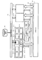
- FIG. 1 is a configuration diagram of an information processing apparatus according to the first embodiment.
- the information processing apparatus 101 is a computer such as a personal computer (PC) or a server.
- CPU central processing unit
- the CPU 111 is a processor (processing unit) that executes various processes.
- the CPU 111 reads and executes the BIOS 172 stored in the BIOS storage area 171. Further, the CPU 111 reads and executes a program stored in the volatile main storage device 121 or the nonvolatile main storage device 141.
- an Operating System (OS) is installed, and the CPU 111 reads the OS from the external storage device 161 to the volatile main storage device 121 and / or the nonvolatile main storage device 141 and executes it.
- OS Operating System
- the CPU 111 has a memory controller 112 and an I / O controller 113.
- the memory controller 112 controls reading / writing with respect to the volatile main storage device 121 and the nonvolatile main storage device 131.
- the memory controller 112 is connected to the volatile main storage device 121 and the nonvolatile main storage device 131 via the memory bus 191. Data in the volatile main storage device 121 and the nonvolatile main storage device 131 are transmitted via the memory bus 192.
- the memory controller 112 is connected to the volatile main storage device 121 and the nonvolatile main storage device 131 via an Inter-Integrated Circuit (I 2 C) bus 192.
- the memory controller 112 also serves as an I 2 C master controller.
- the I / O controller 113 controls the input / output device.
- the I / O controller 113 is connected to the BIOS storage area 171, the external storage device controller 151, and the other input / output device 181 via a peripheral component-interconnect (PCI) bus 193.
- PCI peripheral component-interconnect
- the volatile main storage device 121 is a storage device that stores data using a volatile storage element.
- the volatile main storage device 121 is, for example, a dynamic random access memory (DRAM).
- DRAM dynamic random access memory
- the volatile main storage device 121 is directly accessible from the CPU 111.
- the non-volatile main storage device 131 is a storage device that stores data using a non-volatile storage element.
- the non-volatile main storage device 131 is, for example, a NAND flash memory, a Magnetoresistive Random Access Memory (MRAM), or the like.
- MRAM Magnetoresistive Random Access Memory
- the nonvolatile main storage device 131 can hold data even when power is not supplied.
- the nonvolatile main storage device 131 is directly accessible from the CPU 111.
- the external storage device controller 151 controls the external storage device 161.
- the external storage device controller 151 is connected to the I / O controller 113, the external storage device 161, and the non-volatile memory (NVM) controller 201.
- NVM non-volatile memory
- the external storage device 161 is a nonvolatile storage device that stores data.
- the external storage device 161 cannot be directly accessed from the CPU 111. Therefore, when the CPU 111 reads data from the external storage device 161, the data is transferred to the volatile main storage device 121 or the nonvolatile main storage device 131 and read from the volatile main storage device 121 or the nonvolatile main storage device 131. It is.
- the external storage device 161 is, for example, a hard disk drive, a solid state drive (SSD), or a magnetic tape device.
- the external storage device 161 has a slower access speed than the volatile main storage device 121 and the nonvolatile main storage device 131.
- the external storage device 161 is also called an auxiliary storage device or a secondary storage device.
- the BIOS storage area 171 stores BIOS Flash Firmware (hereinafter referred to as BIOS) 172 and BIOS setting information 173.
- BIOS storage area 171 is, for example, a nonvolatile memory.
- the BIOS 172 is a program for initializing hardware, starting a boot loader, and the like.
- the BIOS 172 performs dump processing, setting of the NVM controller, and the like.
- the BIOS 172 is, for example, Unified Extensible Firmware Interface (UEFI) or extended firmware.
- UEFI Unified Extensible Firmware Interface
- the BIOS 172 is read and executed by the CPU 111.
- the BIOS setting information 173 is information describing setting values used at the time of memory dump processing, characteristics of the main storage devices (the volatile main storage device 121 and the nonvolatile main storage device 131) mounted in the memory slot, and the like.
- the other input / output device 181 is a device for inputting and / or outputting data.
- the other input / output device 181 is, for example, a universal serial bus (USB) device or a peripheral component interconnect (PCI) card.
- USB universal serial bus
- PCI peripheral component interconnect
- FIG. 2 is a diagram illustrating an example of the BIOS setting information.
- the BIOS setting information 173 is described in association with Element, Attribute1, Attribute2, and Value.
- Element indicates the target device or setting item.
- dump destination external storage device As the element, dump destination external storage device, memory manual exchange, and memory slots 1 to 6 are described.
- Attribute1 and Attribute2 indicate device characteristics.
- “shared” is described as Attribute1 of the dump destination external storage device. This indicates that the external storage device is set as a dump destination for a plurality of main storage devices.
- volatile is described as Attribute1 of memory slots 1 to 3
- nonvolatile is described as Attribute1 of memory slots 4 to 6. This indicates that the main storage devices mounted in the memory slots 1 to 3 are volatile and the main storage devices mounted in the memory slots 4 to 6 are nonvolatile.
- Block (non-target) is described as Attribute 2 of the memory slot 4
- “Byte (target)” is described as Attribute 2 of the memory slots 5 and 6. This indicates that block access is performed to the main storage device mounted in the memory slot 4 and that it is not a dump target, byte access is performed to the main storage device mounted in the memory slots 5 and 6, Indicates that it is a dump target.
- Block access visible to the OS as a block storage device
- Byte access visible to the OS as a physical memory space
- N is described as the value of the manual memory replacement. This indicates that manual replacement of the nonvolatile main storage device 131 is not performed. When Y is described, it indicates that the nonvolatile main storage device 131 is manually replaced. “Memory manual replacement” is used in a fourth embodiment described later.
- “Pri” indicates a priority, indicating that the priority of the main storage device mounted in the memory slot 5 is High and the priority of the main storage device mounted in the memory slot 6 is Low.
- FIG. 3 is a diagram showing the configuration of the nonvolatile main memory device and the connection bus according to the first embodiment.
- EEPROM Electrically Erasable Programmable Read-Only Memory
- the NVM controller 201-1 includes a buffer 202, a storage element management table 203, and control firmware 204.
- the NVM controller 201-1 actively copies the dump target data to the external storage device 161 irrespective of the OS operation. Copying is the same as access from the OS, but the minimum access unit is a page, but the efficiency with the protocol with the external storage device 161 being sent in batches within the data length range that can be sent with a single transfer command Plan
- the buffer 202 is a storage device that temporarily stores data to be written to the storage element 251 or data read from the storage element 251.
- the storage element management table 203 is a table in which the state of each page of the nonvolatile main storage device 131-1 is described. Details of the storage element management table 203 will be described later.
- the OS divides the main storage area into units of structures called “pages” by a virtual storage method, and a “page table” exists as a structure for managing them. To do.
- One OS page table is stored in the entire memory space, and is stored using a part of the main storage area, and therefore is not provided for each main storage device.
- the NVM controller 201 of each non-volatile main storage device 131 separately from the page table managed by the OS, holds a unique page table for dump management.
- the size and start position of each page are the same as those managed by the OS.
- the control firmware 204 is a program for performing background (BG) dump routine processing and the like to be described later.
- the control firmware 204 is executed by the NVM controller 201-1.
- nonvolatile main storage devices 131-2 and 131-3 are the same as that of the nonvolatile main storage device 131-1, and therefore the description thereof is omitted.
- the EEPROM 211 stores information such as the characteristics of the nonvolatile main storage device 131-1 and memory dump processing settings. Details of the information stored in the EEPROM 211 will be described later.
- the external storage device controller 231 is connected to the external storage device controller 151 via the connector 241. This connection is not limited to a dump application, but can be used for an application such as realizing a backup in preparation for a failure of a nonvolatile main storage device without applying a load to the OS.
- the external storage device controller 231 transmits and receives data to and from the external storage device controller 151.
- the I / O controller 113 including the Direct Memory Access (DMA) controller and the PCI bus 193 are not affected.
- DMA Direct Memory Access
- the communication protocol with the external storage device 161 may be any type such as Small Computer System Interface (SCSI).
- SCSI Small Computer System Interface
- the external storage device controllers 151 and 231 are implemented not only with a function for simply exchanging communication protocols but also with a level capable of understanding a write position on a block or file system.
- the storage element 251 is an element that stores data.
- FIG. 4 is a diagram illustrating an example of the storage element management table.
- page numbers and flags are associated with each other.
- the page number is a number assigned to the page.
- a page with page number n may be referred to as page n.
- the flag is information indicating the state of the page.
- a free area a used area (Dirty), a used area (Sync), an undumped area, or a Reserved area is described.
- the empty area indicates an empty area where no data is written.
- the used area (Dirty) indicates that data is written and the data is not copied to the external storage device 161, that is, is not dumped.
- the use area (Sync) indicates that data has been written and the data has been copied to the external storage device 161, that is, has been dumped.
- Undumped indicates that it has not been dumped. Also, numbers added after undumped such as undumped (1) and undumped (2) indicate dump generations. If a crash event occurs again during the BG dump process, the dump can be performed again. In this case, in order to make it possible to separate the rest of the previous dump data from the current dump data, the NVM controller 201 sets all used pages as “undumped” at the beginning of executing the BG dump process. When a flag of a page that is already “undumped” is found, it can be distinguished by rewriting it to “undumped (1)”. In this case, the NVM controller 201 performs processing such as making it possible to distinguish the file names of the previous and current dump destinations.
- Reserved indicates that the reserved area is unused (ie, an address viewed from the outside is not allocated).
- FIG. 5 is a diagram showing information recorded in the EEPROM.
- the type of the main storage module the capacity of the main storage module, the presence or absence of ECC, the temperature sensor value, the BG dump flag, and the dump destination external storage device are recorded.
- the type of main storage module indicates the type of main storage device. Specifically, the type of the main storage module indicates whether the main storage device is volatile or nonvolatile. FIG. 5 shows “nonvolatile” since it is the EEPROM 211 of the nonvolatile main memory 131-1.
- the capacity of the main storage module indicates the capacity of the nonvolatile main storage device 131-1.
- the presence / absence of ECC indicates the presence / absence of the error check and correct (ECC) function of the nonvolatile main storage device 131-1.
- the temperature sensor value is the temperature of the nonvolatile main storage device 131-1 acquired from the temperature sensor.
- the BG dump flag indicates whether to perform BG dump processing.
- One of 0 to 2 is set as the BG dump flag. 0 is invalid (that is, BG dump processing is not performed or BG dump processing is completed), 1 is valid (that is, BG dump processing is performed), 2 is valid and Wait (that is, waiting for performing BG dump processing) Indicates.
- the dump destination external storage device indicates a dump destination external storage device.
- the volatile main storage device 121 is also equipped with an EEPROM in which characteristics of the volatile main storage device 121 (type of main storage module, capacity of main storage module, presence / absence of ECC, temperature sensor value, etc.) are recorded. .
- FIG. 6 is a flowchart of the memory dump process according to the first embodiment. First, it is assumed that the OS is executed in the information processing apparatus 101.
- step S501 a crash event, that is, a fatal error occurs in the OS of the information processing apparatus 101.
- step S502 the CPU 111 starts a dump process.
- step S ⁇ b> 503 the CPU 111 sets a BG dump flag of the nonvolatile main storage device 131.
- the CPU 111 refers to the BIOS setting information 173 and confirms the priority (Pri) of each nonvolatile main storage device 131.
- step S504 the NVM controller 201 sets a flag of the storage element management table 203. Specifically, the NVM controller 201 sets “use area (Dirty)” to “undumped”. The NVM controller 201 sets a flag other than “used area (Dirty)” to “free area”.
- step S505 the CPU 111 resets devices other than the nonvolatile main storage device 131 (including the CPU 111 and the volatile main storage device 121).
- step S506 the CPU 111 activates the OS. Thereafter, steps S507 to S510 and step S511 are executed in parallel.
- each NVM controller 201 performs an interrupt dump process.
- the interrupt dump process will be described later.
- Each step executed by the CPU 111 described above is realized by the CPU 111 reading and executing the BIOS 172.
- FIG. 7 is a detailed flowchart of the BG dump process according to the first embodiment.
- FIG. 7 corresponds to step S507 or step S510 in FIG.
- step S521 the NVM controller 201 selects one page to be processed in the following steps S522 to S524 from unselected pages. For example, the NVM controller 201 selects a page with the smallest page number from unselected pages. As a result, pages are selected in the ascending order of page numbers. Hereinafter, the selected page is referred to as a selected page.
- step S522 the NVM controller 201 refers to the storage element management table 203 and checks whether the flag of the selected page is “undumped”. If the flag of the selected page is “undumped”, the control proceeds to step S523, and if not, the control proceeds to step S525.
- step S523 the NVM controller 201 copies (transmits) the data of the selected page to the external storage device 161. As a result, the data of the selected page is written to the external storage device 161.
- step S524 the NVM controller 201 sets the flag of the selected page of the storage element management table 203 to “free space”.
- step S525 if there is an unselected page, control returns to step S521, and if there is no unselected page (ie, there is no page whose flag is “undumped”), control proceeds to step S526.
- step S526 the NVM controller 201 sets the BG dump flag of the EEPROM 211 to 0.
- FIG. 8 is a detailed flowchart of the interrupt dump process according to the first embodiment.
- FIG. 8 corresponds to step S511 in FIG.
- step S531 the NVM controller 201 waits for a write request from the OS. If a write request from the OS has been received, control proceeds to step S532. In addition, when the BG dump process ends, the interrupt dump process ends.
- step S532 the NVM controller 201 refers to the storage element management table 203 and checks whether or not the flag of the write destination page by the write request is “undumped”. If the destination page flag is “undumped”, the control proceeds to step S533, and if it is not “undumped”, the control proceeds to step S534.
- step S533 the NVM controller 201 writes the write request data in the buffer 202 and reports the write completion to the OS (Write Back method). Then, the NVM controller 201 copies (transmits) the write destination page of the write request data to the external storage device 161, and sets the flag of the page to “free space”.
- step S534 the NVM controller 201 writes the write request data to the write destination page (storage element 251). Further, the flag of the page in which the data is written becomes “use area (Dirty)”. Then, the control returns to step S531.
- FIG. 9 is a diagram illustrating interrupt dump processing according to the first embodiment.
- FIG. 9 shows processing when the page to be written is undumped.
- the NVM controller 201 receives a write request from the OS (step S541).
- the NVM controller 201 generates a queue for writing the data of the write destination page to the external storage device 161, and interrupts the head of the queue waiting for the turn.
- the NVM controller 201 writes the write request data to the write destination page (storage element 251).
- a queue for sequentially dumping pages is generated by the BG dump process.
- the generated queues are arranged in the order of generation, and are transmitted to the external storage device controller 151 sequentially from the top.
- interrupt dump processing By using interrupt dump processing, the first data write from the OS is slow, but subsequent read / write to the same page can be as fast as the normal nonvolatile main memory. Moreover, fragmentation (fragmentation) occurs in the dump file by interrupting the dump or by asynchronously dumping from a plurality of nonvolatile main storage devices. By recording the start address and the offset together at the location where the dump file becomes discontinuous, it is possible to restore to the correct address space at the time of dump analysis.
- the significance of the gradual BG memory dump processing based on such priority will be described. Due to the characteristics of OS memory management, the physical memory address determined by the BIOS is expected to have locality in the access order and frequency. In particular, it is necessary to preferentially dump an area used by the kernel when starting the OS. By retaining such characteristics in the BIOS setting information 173 as a profile and prioritizing in units of the nonvolatile main storage device 131, the area used by the kernel can be dumped preferentially.
- nonvolatile main storage devices 1 to N there are nonvolatile main storage devices 1 to N, and kernel space is assigned to the nonvolatile main storage devices 1 and 2, and user process space is assigned to the nonvolatile main storage devices 3 to N.
- the priority of the nonvolatile main storage devices 1 and 2 is set to High, and the priority of the nonvolatile main storage devices 3 to N is set to Low.
- BG dump flag 1 (valid) is set in .about.N (second stage).
- the NVM controller 201 performs dump only when performing interrupt dump processing in response to a write request from the OS.
- the portion of the main storage devices 3 to N in the second stage of dumping that is shaded in a broken line indicates the area that has been dumped by the interrupt dump process.
- FIG. 11 is a diagram showing a state of the storage element management table immediately before the occurrence of the crash event and immediately after setting the BG dump flag according to the first embodiment.
- each record of the storage element management table 203 is described so as to correspond to the physical position (Column, Row) of the storage element.
- the NVM controller 201 sets the flag of the storage element management table 203 (step S504). As shown in the lower part of FIG. 11, the “use area (Dirty)” is set to “undumped”.
- the information processing apparatus of the first embodiment it is possible to shorten the business stop time due to the memory dump process.
- the dumping process from the nonvolatile main storage device to the external storage device is performed as a background process after restarting the OS, so that the business stop time can be shortened.
- the configuration of the information processing apparatus according to the second embodiment is the same as that of the first information processing apparatus unless otherwise specified, and a description thereof will be omitted.
- the nonvolatile main storage device 131 of the second embodiment seems to have storage elements variably assigned to addresses viewed from the outside, such as those used in SSDs using NAND flash memory. It is assumed that a simple method is implemented.
- Such a nonvolatile main storage device 131 cannot directly update data held by a certain storage element, but writes data to another storage element or rewrites a group of storage element columns after erasure. I do.
- the non-volatile main storage device 131 since the life of the memory element depends on the number of times of writing, the non-volatile main storage device 131 is not internally used even if the addresses are continuous from the outside so that writing to a specific memory element is not biased. It has a function called wear leveling that writes to continuous areas. For this reason, the nonvolatile main storage device 131 has a table for managing the correspondence between addresses viewed from the outside and storage elements.
- the storage element management table 203 of the first embodiment is expanded to realize a table for managing the correspondence between addresses and storage elements viewed from the outside.
- FIG. 12 is a diagram illustrating a state of the nonvolatile main memory device according to the second embodiment.
- the nonvolatile main storage device 131 according to the second embodiment includes an effective storage element used for reading and writing data, and a wear leveling storage element used for wear leveling.
- the non-volatile main storage device 131 according to the second embodiment actually has a storage element for wear leveling that is approximately several tens of percent more than the capacity of the non-volatile main storage device 131 viewed from the outside.
- the non-volatile main storage device 131 of the second embodiment has a storage element management table that is an extension of the storage element management table 203, instead of the storage element management table 203.
- an extended storage element management table 203 ' a storage element management table obtained by expanding the storage element management table 203 of the first embodiment is referred to as an extended storage element management table 203 '.
- FIG. 13 is an example of an extended storage element management table.
- the extended storage element management table 203 ′ is described in association with a physical address range, a used storage element position, a page number, and a flag viewed from the outside.
- the physical address range seen from the outside is the physical address range of the nonvolatile main storage device 131 seen from the outside (OS or memory controller 112).
- the used storage element position indicates the position of the storage element 251 of the nonvolatile main storage device 131.
- the page number is a number assigned to the page.
- the flag is information indicating the state of the page.
- the memory dump process and the BG dump process are the same as those in the first embodiment.
- the following interrupt dump process is performed instead of the interrupt dump process of FIG.
- FIG. 14 is a detailed flowchart of the interrupt dump process according to the second embodiment.
- FIG. 14 corresponds to step S511 in FIG.
- step S601 the NVM controller 201 waits for a write request from the OS. If a write request from the OS is received, control proceeds to step S602. In addition, when the BG dump process ends, the interrupt dump process ends.
- step S602 the NVM controller 201 refers to the extended storage element management table 203 'and checks whether or not the flag of the page including the write destination memory address is “undumped”. If the flag of the page including the write destination memory address is “undumped”, the control proceeds to step S603, and if not “undumped”, the control proceeds to step S605.
- step S603 the NVM controller 201 invalidates the physical address range viewed from the outside including the write destination memory address. Specifically, the NVM controller 201 writes “invalid” in the physical address range viewed from the outside including the memory address of the write destination of the extended storage element management table 203 ′.
- step S604 the NVM controller 201 allocates the invalid physical address range viewed from the outside to the unallocated storage element. Specifically, the NVM controller 201 invalidates the physical memory address range and page number viewed from the outside corresponding to the used storage element position of the unallocated storage element in the extended storage element management table 203 ′ from the outside. Write the physical address range and the page number of the invalidated page.
- step S605 the NVM controller 201 writes the write request data to the newly assigned page. Further, the flag of the page in which the data is written becomes “use area (Dirty)”. Control then returns to step 601.
- FIG. 15 is a diagram showing an extended storage element management table before and after the allocation change.
- the used storage element position corresponding to the physical memory address range 0x01010000 to 0x0101FFFF viewed from the outside is 0x1254, the page number is 20, and the flag Is not dumped.
- the NVM controller 201 looks from the outside including the write destination memory address of the extended storage element management table 203 ′. Write "invalid" to the specified physical address range.
- the range of the physical memory address viewed from the outside corresponding to the invalid page is 0x01010000 to 0x0101FFFF (invalid).
- the NVM controller 201 uses an externally viewed physical memory that is invalidated to the physical address range and page number viewed from the outside corresponding to the used storage element position of the unallocated storage element in the extended storage element management table 203 ′. Write the address range and the page number of the invalidated page. The NVM controller 201 writes the write request data to the newly assigned page, and sets the flag to “used area (Dirty)”.
- the BG dump process is sequentially executed asynchronously with the interrupt dump process, the address data itself is retained so that the original address range can be discriminated later. After dumping, the address range and page number of the storage element are changed to unallocated and pooled for wear leveling.
- the information processing apparatus of the second embodiment it is possible to reduce the operation stop time due to the memory dump process.
- performance deterioration is less likely to occur compared to the first embodiment by executing write processing from the OS and dump processing asynchronously. .
- the configuration of the information processing apparatus according to the third embodiment is the same as the configuration of the first information processing apparatus unless otherwise specified, and a description thereof will be omitted.
- “used area (Sync)” is further used as a flag of the storage element management table.
- the normal backup process is as follows.
- the NVM controller 201 monitors the storage element management table 203 and checks whether there is a page whose flag is “used area (Dirty)”.
- the NVM controller 201 When the NVM controller 201 detects a page whose flag is “used area (Dirty)”, the NVM controller 201 writes the data of the page to the external storage device 161 (backup).
- the NVM controller 201 sets the flag of the page to “use area (Sync)”.
- the NVM controller 201 When the NVM controller 201 writes data to a page in response to a write request from the OS, the NVM controller 201 sets the page flag to “usable area (Dirty)”.
- the NVM controller 201 always monitors the storage element management table 203, and performs backup so as to reduce the number of pages whose flag is “used area (Dirty)”.
- the memory dump process of the third embodiment is basically the same as the memory dump process (FIG. 6) of the first embodiment.
- FIG. 16 is a diagram showing the state of the storage element management table immediately before the occurrence of the crash event and immediately after setting the BG dump flag according to the third embodiment.
- FIG. 16 shows the state of the storage element management table immediately before the occurrence of the crash event, and the lower side shows the state of the storage element management table immediately after the BG dump flag is set.
- each record of the storage element management table 203 is described so as to correspond to the physical position (Column, Row) of the storage element.
- the flags of pages 1 and 6 are “use area (Dirty)”, and the flags of pages 2, 3, and X ⁇ 1 are “use area (Sync)”.
- the flags of 5 and X are “free space”.
- the memory dump process of the third embodiment is the same as the memory dump process of the first embodiment.
- the NVM controller 201 sets a flag of the storage element management table 203 (step S504). As shown in the lower part of FIG. 16, “used area (Dirty)” is set to “undumped” and “used area (Sync)” is set to “free area”.
- the page of flag usage area (Sync) has already been backed up in the external storage device 161, so there is no need to dump it.
- the time for the memory dump process can be shortened compared to the first embodiment.
- the information processing apparatus of the third embodiment it is possible to reduce the operation stop time due to the memory dump process.
- the information processing apparatus of the third embodiment since the backup is collected at the normal time, only the difference from the backup needs to be dumped at the time of the memory dump process, so that the time of the memory dump process can be reduced. it can.
- the configuration of the information processing apparatus according to the fourth embodiment is the same as that of the first information processing apparatus unless otherwise specified, and a description thereof will be omitted.
- 18A and 18B are flowcharts of the memory dump process according to the fourth embodiment. First, it is assumed that the OS is executed in the information processing apparatus 101.
- step S701 a crash event, that is, a fatal error occurs in the OS of the information processing apparatus 101.
- step S702 the CPU 111 starts a dump process. Thereafter, the volatile main storage device dump routine (steps S703 to S707) and the non-volatile main storage device flag setting process (steps S708 to S712) are executed in parallel. Note that the volatile main storage device dump routine and the nonvolatile main storage device flag setting process may be executed in series, or either one may be executed first.
- step S703 the CPU 111 starts a foreground volatile main memory dump routine (foreground dump).
- foreground indicates a state in which the information processing apparatus 101 operates exclusively for dump processing and the business is not operating.
- the CPU 111 refers to the EEPROM of the main storage device (the volatile main storage device 121 and the nonvolatile main storage device 131) to determine whether the main storage device is volatile or nonvolatile.
- step S704 the CPU 111 checks whether there is a free area in the nonvolatile main storage device 131 that can copy all data or a part of the data in the volatile main storage device 121. If there is a free area where data in the volatile main storage device 121 can be copied, control proceeds to step S705. If there is no free area where data in the volatile main storage device 121 can be copied, control proceeds to step S706.
- step S705 the CPU 111 copies (writes) the data in the volatile main storage device 121 to the nonvolatile main storage device 131.
- the CPU 111 adds additional information (for example, copied data) so that the original memory address of the volatile main storage device can be determined later.
- additional information for example, copied data
- step S706 If there is no free space in the nonvolatile main storage device 131 during copying, the control proceeds to step S706, and the data in the volatile main storage device 121 that has not been copied is copied to the external storage device 161.
- step S706 the CPU 111 copies (writes) data in the volatile main storage device 121 to the external storage device 161.
- step S707 the CPU 111 ends the volatile main storage device dump routine.
- the free area of the nonvolatile main storage device 131 can be implemented as reserved in advance, and the volatile main storage device dump routine dynamically changes to the free area that changes depending on the state at the time of the occurrence of the crash event. It is desirable to be mounted so that
- step S708 the CPU 111 starts a nonvolatile main storage device flag setting process.
- step S709 the CPU 111 refers to the BIOS setting information 173 and checks whether the nonvolatile main storage device 131 is a block access. If the nonvolatile main storage device 131 is block access, control proceeds to step S710. If the nonvolatile main storage device 131 is not block access (byte access), control proceeds to step S711. The above check is performed for all the nonvolatile main storage devices 131.
- step S710 the CPU 111 excludes the nonvolatile main storage device 131 that is block access from being dumped.
- the NVM controller 201 in which the BG dump flag is set sets a flag in the storage element management table 203. Specifically, the NVM controller 201 sets “use area (Dirty)” to “undumped”. The NVM controller 201 sets a flag other than “used area (Dirty)” to “free area”.
- step S712 the CPU 111 ends the nonvolatile main storage device flag setting process.
- step S713 the CPU 111 determines whether to manually replace the nonvolatile main storage device 131. Specifically, the CPU 111 refers to the BIOS setting information 173 and determines whether or not to manually replace the volatile main storage device 131 depending on whether “manual replacement” is Y or N. If manual replacement is performed, control proceeds to step S714. If manual replacement is not performed, control proceeds to step S717.
- step S714 the CPU 111 turns off the information processing apparatus 101.
- the CPU 111 sends an event notification from the BIOS to the Baseboard ⁇ ⁇ Management ⁇ ⁇ Controller (BMC) that manages the information processing apparatus 101 at the timing of starting the dump process and turning off the power. Notify maintenance personnel using methods such as Simple Network Management Protocol (SNMP) traps and email.
- BMC Baseboard ⁇ ⁇ Management ⁇ ⁇ Controller
- step S715 the maintenance person manually replaces the nonvolatile main storage device 131 and turns on the information processing apparatus 101.
- the maintenance staff dumps the data of the nonvolatile main storage device removed by the computer prepared separately at the site or the support center, and obtains the dump data necessary for the analysis by merging with the data dumped in the external storage device 161 .
- the maintenance staff obtains a decryption code with the consent of the owner of the information processing device 101.
- step S716 the CPU 111 activates the OS.
- step S717 the CPU 111 resets the CPU 111 and the volatile main storage device 121 so that the memory address space of the nonvolatile main storage device 131 does not disappear.
- step S718 the CPU 111 activates the OS.
- step S719 the CPU 111 and the NVM controller 201 execute a BG dump process.
- step S719 for example, the processing of steps S507 to S510 in FIG. 6 is executed.
- the BG dump process is performed in the nonvolatile main storage device 131 in which the BG dump flag is set in step S711.
- each NVM controller 201 performs an interrupt dump process.
- the interrupt dump process is as described with reference to FIG. 8 or FIG.
- Each step executed by the CPU 111 described above is realized by the CPU 111 reading and executing the BIOS 172.
- the dump data obtained as described above becomes a file with different acquisition timings and addresses. Therefore, it is merged with a separately prepared software tool, or dump analysis software that can read a separate file is used.
- FIG. 19 is a diagram illustrating data positions at the time of each process according to the fourth embodiment.
- the nonvolatile main storage device 131-1 is assumed to be block access, and the nonvolatile main storage device 131-1 is assumed to be byte access. Further, the description of the nonvolatile main storage device 131-3 is omitted.
- the volatile main storage device 121-1 is shown, and the volatile main storage devices 121-2 and 121-3 are omitted.
- the nonvolatile main storage device 131-1 stores data A and B.
- the nonvolatile main storage device 131-2 stores data C and has a free area (Free).
- the volatile main storage device 121-1 stores data D and E (the state at the time of occurrence of the crash event in FIG. 19).
- the data A and B in the nonvolatile main storage device 131-1 are held until the background dump is completed.
- the volatile main storage device dump routine (foreground dump) is started, and the data D of the volatile main storage device 121-1 is copied to the nonvolatile main storage device 131-2 (during the foreground dump in FIG. 19). In addition, the empty area of the nonvolatile main storage device 131-2 disappears by copying the data D to the nonvolatile main storage device 131-2.
- the data E of the volatile main storage device 121-1 is copied to the external storage device 161 (foreground dump completion in FIG. 19).
- step S719 When the OS is restarted (step S718) and the BG dump process is executed (step S719), the data C and D in the nonvolatile main storage device 131-2 are copied to the external storage device 161. Further, the restarted OS data F and G are written to the volatile main storage device 121-1, and the restarted OS data H are written to the nonvolatile main storage device 131-2 (see FIG. 19). During a grand dump).
- the volatile main storage device 121-1 stores data F and G
- the non-volatile main storage device 131-2 stores data H
- the area is an empty area (background dump in FIG. 19 is completed).
- the information processing apparatus of the fourth embodiment it is possible to reduce the operation stop time due to the memory dump process.
- the block access nonvolatile main storage device does not require dumping, wasteful processing can be eliminated by controlling this so that it is excluded from dumping.
- the foreground dump is required by copying the data in the volatile main storage device to a free area in the nonvolatile main storage that can be accessed faster than the external storage device. Time can be shortened.
- the operation stop time can be shortened by setting the dump process from the nonvolatile main storage device to the external storage device as the background process after restarting the OS. .
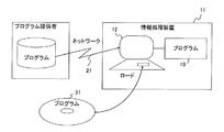
- FIG. 20 is a configuration diagram of a computer system.
- the memory dump process as described above can naturally be realized by a general computer system.
- the information processing apparatus 11 for realizing the memory dump process according to the embodiment includes a main body 12 and a memory 13.
- the memory 13 corresponds to a storage device such as a volatile main storage device 121, a nonvolatile main storage device 131, an external storage device 161, and a BIOS storage area 171.
- the memory 13 stores a program for performing the memory dump process of each embodiment and the like, and the program is executed by the main body 12, whereby various processes of the embodiment can be realized.
- Such a program can also be loaded into the information processing apparatus 11 via the network 21 from the program provider side.
- the program is stored in a portable storage medium 31 that is commercially available and distributed.
- a portable storage medium 31 is set in the information processing apparatus 11, read into the memory 13, and executed by the main body 12. It is also possible.
- Various types of storage media such as CD-ROMs, flexible disks, optical disks, and magneto-optical disks can be used as the portable storage medium 31, and the program code itself read from such a storage medium is an embodiment. Realize the function.
Landscapes
- Engineering & Computer Science (AREA)
- Theoretical Computer Science (AREA)
- Physics & Mathematics (AREA)
- General Engineering & Computer Science (AREA)
- General Physics & Mathematics (AREA)
- Quality & Reliability (AREA)
- Human Computer Interaction (AREA)
- Health & Medical Sciences (AREA)
- Biomedical Technology (AREA)
- Computer Security & Cryptography (AREA)
- Debugging And Monitoring (AREA)
- Techniques For Improving Reliability Of Storages (AREA)
Abstract
オペレーティングシステムを実行する処理部と、前記処理部が直接アクセス可能且つコントローラを有する不揮発性主記憶装置と、前記処理部が直接アクセス可能でない外部記憶装置と、を備え、前記処理部が前記オペレーティングシステムのエラーを検出したとき、前記処理部は、前記不揮発性主記憶装置以外をリセットして、前記オペレーティングシステムを再起動し、前記コントローラは、前記不揮発性主記憶装置のデータを前記外部記憶装置に書き込むことを特徴とする情報処理装置。
Description
本発明は、情報処理装置、メモリダンプ方法、およびメモリダンププログラムに関する。
近年、UNIX(登録商標)サーバ、IAサーバが基幹システムに導入されるようになり、UNIX(登録商標)サーバ、IAサーバの高可用性が重要視されている。一般的に、システムに致命的なエラー(クラッシュ事象)が発生した場合はシステムを緊急停止(パニック)させて、その原因を調査するためにメモリダンプをディスクに保存している。
システムを停止している間は、システムを使用できないので、速やかにシステムを再起動して業務停止時間を短縮することが重要な要件となる。
しかし、近年では、実装メモリの容量がテラバイト(TB)オーダのサーバが登場し、このようなシステムでは、メモリダンプを採取するのに非常に時間がかかり、速やかにシステムを再起動することができなくなっている。
本発明の課題は、メモリダンプ処理による業務停止時間を短縮することである。
実施の形態の情報処理装置は、処理部と、不揮発性主記憶装置と、外部記憶装置と、を備える。
前記処理部は、オペレーティングシステムを実行する。
前記不揮発性主記憶装置は、前記処理部が直接アクセス可能且つコントローラを有する。
前記外部記憶装置は、前記処理部が直接アクセス可能でない。
前記不揮発性主記憶装置は、前記処理部が直接アクセス可能且つコントローラを有する。
前記外部記憶装置は、前記処理部が直接アクセス可能でない。
前記処理部は、前記オペレーティングシステムのエラーを検出したとき、前記不揮発性主記憶装置以外をリセットして、前記オペレーティングシステムを再起動する。
前記コントローラは、前記不揮発性主記憶装置のデータを前記外部記憶装置に書き込む。
実施の形態の情報処理装置によれば、メモリダンプ処理による業務停止時間を短縮することができる。
以下、図面を参照しながら実施の形態について説明する。
図1は、第1の実施の形態に係る情報処理装置の構成図である。
図1は、第1の実施の形態に係る情報処理装置の構成図である。
情報処理装置101は、例えば、パーソナルコンピュータ(PC)やサーバ等のコンピュータである。
情報処理装置101は、Central Processing Unit(CPU)111、揮発性主記憶装置121-i(i=1~3)、不揮発性主記憶装置131-i、外部記憶装置コントローラ151、外部記憶装置161、Basic Input/Output System(BIOS)格納域171、およびその他入出力装置181を備える。
CPU111は、各種処理を実行するプロセッサ(処理部)である。
CPU111は、BIOS格納域171に格納されているBIOS172を読み出して実行する。また、CPU111は、揮発性主記憶装置121または不揮発性主記憶装置141に格納されているプログラムを読み出して実行する。
CPU111は、BIOS格納域171に格納されているBIOS172を読み出して実行する。また、CPU111は、揮発性主記憶装置121または不揮発性主記憶装置141に格納されているプログラムを読み出して実行する。
情報処理装置101には、Operating System(OS)がインストールされており、CPU111は、外部記憶装置161からOSを揮発性主記憶装置121および/または不揮発性主記憶装置141に読み出して実行する。
CPU111は、メモリコントローラ112およびI/Oコントローラ113を有する。
メモリコントローラ112は、揮発性主記憶装置121および不揮発性主記憶装置131に対する読み書きの制御を行う。メモリコントローラ112は、メモリバス191を介して揮発性主記憶装置121および不揮発性主記憶装置131と接続している。揮発性主記憶装置121および不揮発性主記憶装置131のデータは、メモリバス192を介して送信される。
また、メモリコントローラ112は、Inter-Integrated Circuit(I2C)バス192を介して揮発性主記憶装置121および不揮発性主記憶装置131と接続している。メモリコントローラ112は、I2Cのマスタコントローラを兼ねている。
I/Oコントローラ113は、入出力装置の制御を行う。I/Oコントローラ113は、Peripheral Component Interconnect(PCI)バス193を介して、BIOS格納域171、外部記憶装置コントローラ151、およびその他入出力装置181と接続している。
揮発性主記憶装置121は、揮発性の記憶素子を用いたデータを格納する記憶装置である。揮発性主記憶装置121は、例えば、Dynamic Random Access Memory(DRAM)である。
揮発性主記憶装置121は、CPU111から直接アクセス可能である。
揮発性主記憶装置121は、CPU111から直接アクセス可能である。
不揮発性主記憶装置131は、不揮発性の記憶素子を用いたデータを格納する記憶装置である。不揮発性主記憶装置131は、例えば、NAND型フラッシュメモリやMagnetoresistive Random Access Memory(MRAM)等である。
不揮発性主記憶装置131は、電力が供給されない場合でも、データを保持することができる。
不揮発性主記憶装置131は、CPU111から直接アクセス可能である。
不揮発性主記憶装置131は、CPU111から直接アクセス可能である。
外部記憶装置コントローラ151は、外部記憶装置161を制御する。外部記憶装置コントローラ151は、I/Oコントローラ113、外部記憶装置161、およびNonVolatile Memory(NVM)コントローラ201と接続している。
外部記憶装置161は、データを格納する不揮発性の記憶装置である。
外部記憶装置161は、CPU111から直接アクセスできない。よって、CPU111が外部記憶装置161のデータを読み出す場合、該データは、揮発性主記憶装置121または不揮発性主記憶装置131に転送され、揮発性主記憶装置121または不揮発性主記憶装置131から読み出される。
外部記憶装置161は、CPU111から直接アクセスできない。よって、CPU111が外部記憶装置161のデータを読み出す場合、該データは、揮発性主記憶装置121または不揮発性主記憶装置131に転送され、揮発性主記憶装置121または不揮発性主記憶装置131から読み出される。
外部記憶装置161は、例えば、ハードディスクドライブ、Solid State Drive (SSD)、または磁気テープ装置等である。外部記憶装置161は、揮発性主記憶装置121および不揮発性主記憶装置131よりもアクセス速度が遅い。
外部記憶装置161は、補助記憶装置または二次記憶装置とも呼ばれる。
BIOS格納域171は、BIOS Flash Firmware(以下、BIOSと表記する)172およびBIOS設定情報173を格納する。BIOS格納域171は、例えば、不揮発性のメモリである。
BIOS格納域171は、BIOS Flash Firmware(以下、BIOSと表記する)172およびBIOS設定情報173を格納する。BIOS格納域171は、例えば、不揮発性のメモリである。
BIOS172は、ハードウェアの初期化やブートローダーの起動等を行うプログラムである。また、BIOS172は、ダンプ処理やNVMコントローラの設定等を行う。
BIOS172は、例えば、Unified Extensible Firmware Interface(UEFI)や拡張ファームウェア等である。
BIOS172は、CPU111により読み出されて実行される。
BIOS設定情報173は、メモリダンプ処理時に使用する設定値やメモリスロットに搭載される主記憶装置(揮発性主記憶装置121および不揮発性主記憶装置131)の特性などが記載される情報である。
BIOS設定情報173は、メモリダンプ処理時に使用する設定値やメモリスロットに搭載される主記憶装置(揮発性主記憶装置121および不揮発性主記憶装置131)の特性などが記載される情報である。
尚、BIOS設定情報173の詳細については後述する。
その他入出力装置181は、データの入力および/または出力を行う装置である。その他入出力装置181は、例えば、Universal Serial Bus(USB)デバイスやPeripheral Component Interconnect(PCI)カード等である。
その他入出力装置181は、データの入力および/または出力を行う装置である。その他入出力装置181は、例えば、Universal Serial Bus(USB)デバイスやPeripheral Component Interconnect(PCI)カード等である。
図2は、BIOS設定情報の例を示す図である。
BIOS設定情報173は、Element、Attribute1、Attribute2、およびValueが対応付けられて記載されている。
BIOS設定情報173は、Element、Attribute1、Attribute2、およびValueが対応付けられて記載されている。
Elementは、対象の装置や設定項目を示す。図2において、Elementとして、ダンプ先外部記憶装置、メモリ手動交換、メモリスロット1~6が記載されている。
Attribute1およびAttribute2は、装置の特性を示す。図2において、ダンプ先外部記憶装置のAttribute1として、「共有」が記載されている。これは、外部記憶装置が複数の主記憶装置のダンプ先として設定されていることを示す。
また、図2において、メモリスロット1~3のAttribute1として「揮発性」、メモリスロット4~6のAttribute1として「不揮発性」が記述されている。これは、メモリスロット1~3に搭載されている主記憶装置が揮発性、メモリスロット4~6に搭載されている主記憶装置が不揮発性であることを示す。
また、図2において、メモリスロット4のAttribute2として「Block(対象外)」、モリスロット5、6のAttribute2として「Byte(対象)」が記述されている。これは、メモリスロット4に搭載されている主記憶装置に対してブロックアクセスを行い、ダンプ対象でないことを示し、メモリスロット5、6に搭載されている主記憶装置に対してバイトアクセスを行い、ダンプ対象であることを示す。
不揮発性主記憶装置131へのアクセス方法は以下2種類ある。
(1)ブロックアクセス:OSからブロックストレージデバイスとして見える
(2)バイトアクセス:OSから物理メモリ空間として見える
(1)ブロックアクセス:OSからブロックストレージデバイスとして見える
(2)バイトアクセス:OSから物理メモリ空間として見える
Valueは、設定されている値である。
図2において、メモリ手動交換のValueとして、Nが記載されている。これは、不揮発性主記憶装置131の手動交換を行わないことを示す。尚、Yが記載されている場合は、不揮発性主記憶装置131の手動交換を行うことを示す。尚、「メモリ手動交換」は、後述の第4の実施の形態で利用される。
図2において、メモリ手動交換のValueとして、Nが記載されている。これは、不揮発性主記憶装置131の手動交換を行わないことを示す。尚、Yが記載されている場合は、不揮発性主記憶装置131の手動交換を行うことを示す。尚、「メモリ手動交換」は、後述の第4の実施の形態で利用される。
図2において、ダンプ先外部記憶装置のValueとして、Ctrl=0, Device=2が記載されている。Ctrl=0, Device=2は、ダンプ先の外部記憶装置161を識別する情報である。
また、図2において、メモリスロット5のValueとして「Pri=High」、メモリスロット6のValueとして「Pri=Low」が記載されている。「Pri」は優先度を示し、メモリスロット5に搭載されている主記憶装置の優先度がHigh、メモリスロット6に搭載されている主記憶装置の優先度がLowであることを示している。
図3は、第1の実施の形態に係る不揮発性主記憶装置の構成および接続バスを示す図である。
不揮発性主記憶装置131-1は、NVMコントローラ201-1、Electrically Erasable Programmable Read-Only Memory(EEPROM)211、外部記憶装置コントローラ231、コネクタ241、および記憶素子251-k(k=1~8)
NVMコントローラ201-1は、バッファ202、記憶素子管理テーブル203、および制御ファームウェア204を備える。
NVMコントローラ201-1はOSの動作とは無関係に、ダンプ対象のデータを能動的に外部記憶装置161にコピーする。コピーはOSからのアクセス同様、最小アクセス単位はページだが、外部記憶装置161とのプロトコルが一度の転送命令で送信可能なデータ長の範囲で、複数のページが一括して送信されることで効率化を図る。
バッファ202は、記憶素子251に書き込むデータまたは記憶素子251から読み出したデータを一時的に格納する記憶装置である。
記憶素子管理テーブル203は、不揮発性主記憶装置131-1の各ページの状態が記載されたテーブルである。
尚、記憶素子管理テーブル203の詳細については後述する。
尚、記憶素子管理テーブル203の詳細については後述する。
実施の形態の情報処理装置101では、仮想記憶方式によりOSが主記憶領域を「ページ」と呼ばれる構造体の単位で分割し、それらを管理するための構造として「ページテーブル」が存在するものとする。OSのページテーブルはメモリ空間全体でひとつ保持され、主記憶領域の一部を利用して格納されるため、主記憶装置毎に持つものではない。一方、OSが管理するページテーブルとは別に、個々の不揮発性主記憶装置131のNVMコントローラ201は、ダンプ管理のために独自のページテーブルを保持するものとする。また、各ページのサイズおよび開始位置はOSが管理するものと一致するものとする。
制御ファームウェア204は、後述するBackground(BG)ダンプルーチン処理等を行うプログラムである。制御ファームウェア204は、NVMコントローラ201-1により実行される。
尚、不揮発性主記憶装置131-2、131-3の構成は、不揮発性主記憶装置131-1の構成と同様であるため説明は省略する。
EEPROM211は、不揮発性主記憶装置131-1の特性やメモリダンプ処理の設定などの情報を格納する。尚、EEPROM211に格納される情報の詳細については後述する。
外部記憶装置コントローラ231は、コネクタ241を介して、外部記憶装置コントローラ151と接続する。この接続はダンプ用途に限らず、不揮発性主記憶装置の故障に備えたバックアップを、OSに負荷をかけずに実現するなどの用途に流用することも可能である。外部記憶装置コントローラ231は、外部記憶装置コントローラ151との間でデータの送受信を行う。外部記憶装置コントローラ231と外部記憶装置コントローラ151との間で通信を行うことで、Direct Memory Access(DMA)コントローラを含むI/Oコントローラ113やPCIバス193に影響が生じなくなる。
外部記憶装置161との通信プロトコルはSmall Computer System Interface(SCSI)など任意のものでよい。外部記憶装置コントローラ151、231は単純に通信プロトコルをやりとりする機能だけでなく、ブロックまたはファイルシステム上の書き込み位置を理解可能なレベルのものが実装される。
記憶素子251は、データを格納する素子である。
図4は、記憶素子管理テーブルの例を示す図である。
図4は、記憶素子管理テーブルの例を示す図である。
記憶素子管理テーブル203には、ページ番号とフラグが対応付けられて記載されている。
ページ番号は、ページに割り当てられた番号である。尚、以下の説明において、ページ番号nのページをページnと表記する場合がある。
フラグは、ページの状態を示す情報である。フラグとして、空き領域、使用領域(Dirty)、使用領域(Sync)、未ダンプ、またはReservedが記載される。
空き領域は、データが書き込まれていない空き領域であることを示す。
使用領域(Dirty)は、データが書き込まれており、且つ該データは外部記憶装置161へコピーされていない、すなわち未ダンプであることを示す。
使用領域(Dirty)は、データが書き込まれており、且つ該データは外部記憶装置161へコピーされていない、すなわち未ダンプであることを示す。
使用領域(Sync)は、データが書き込まれており、該データは外部記憶装置161へコピー済み、すなわちダンプ済みであることを示す。
未ダンプは、ダンプされていないことを示す。また、未ダンプ(1)、未ダンプ(2)のような未ダンプの後ろに付加されている数字は、ダンプの世代を示す。BGダンプ処理中に再度クラッシュ事象が発生した場合も再度ダンプは可能である。この場合、前回のダンプデータの残りと今回のダンプデータの分離を可能とするために、NVMコントローラ201がBGダンプ処理を実行する初期にすべての使用済みページを「未ダンプ」と設定する処理で、すでに「未ダンプ」となっているページのフラグを見つけた場合「未ダンプ(1)」に書き換えることで、区別を可能とする。この場合、NVMコントローラ201は前回と今回のダンプ先のファイル名を区別可能なようにするなどの処理を行う。同様に前々回の未ダンプデータは「未ダンプ(2)」などとインクリメントすることで複数世代の管理も可能であるが、フラグの実装上どれだけ未アサインの番号が存在するかが世代の上限となる。例えば、フラグが4ビット(16値)で管理され、4値が既存のフラグとしてアサイン済みであれば、追加で最大12世代分が管理可能である。
Reservedは、未使用の(すなわち、外部から見たアドレスが割り当てられていない)予備領域であることを示す。
図5は、EEPROMに記録されている情報を示す図である。
EEPROM211には、主記憶モジュールの種類、主記憶モジュールの容量、ECCの有無、温度センサ値、BGダンプフラグ、およびダンプ先外部記憶装置が記録されている。
EEPROM211には、主記憶モジュールの種類、主記憶モジュールの容量、ECCの有無、温度センサ値、BGダンプフラグ、およびダンプ先外部記憶装置が記録されている。
主記憶モジュールの種類は、主記憶装置の種類を示す。詳細には、主記憶モジュールの種類は、主記憶装置が揮発性か不揮発性であるかを示す。図5は、不揮発性主記憶装置131-1のEEPROM211なので、「不揮発性」が記載されている。
主記憶モジュールの容量は、不揮発性主記憶装置131-1の容量を示す。
ECCの有無は、不揮発性主記憶装置131-1のError Check and Correct(ECC)機能の有無を示す。
ECCの有無は、不揮発性主記憶装置131-1のError Check and Correct(ECC)機能の有無を示す。
温度センサ値は、温度センサから取得した不揮発性主記憶装置131-1の温度である。
BGダンプフラグは、BGダンプ処理を行うか否かを示す。BGダンプフラグは0~2のいずれかが設定される。0は無効(すなわち、BGダンプ処理を行わない、若しくはBGダンプ処理完了)、1は有効(すなわち、BGダンプ処理を行う)、2は有効且つWait(すなわち、BGダンプ処理を行うために待機)を示す。
ダンプ先外部記憶装置は、ダンプ先の外部記憶装置を示す。
尚、揮発性主記憶装置121にも揮発性主記憶装置121の特性(主記憶モジュールの種類、主記憶モジュールの容量、ECCの有無、温度センサ値等)が記録されたEEPROMが搭載されている。
尚、揮発性主記憶装置121にも揮発性主記憶装置121の特性(主記憶モジュールの種類、主記憶モジュールの容量、ECCの有無、温度センサ値等)が記録されたEEPROMが搭載されている。
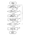
図6は、第1の実施の形態に係るメモリダンプ処理のフローチャートである。
先ず、情報処理装置101では、OSが実行されているものとする。
先ず、情報処理装置101では、OSが実行されているものとする。
ステップS501において、情報処理装置101のOSでクラッシュ事象、すなわち致命的なエラーが発生する。
ステップS502において、CPU111は、ダンプ処理を開始する。
ステップS503において、CPU111は、不揮発性主記憶装置131のBGダンプフラグを設定する。詳細には、CPU111は、BIOS設定情報173を参照し、各不揮発性主記憶装置131の優先度(Pri)を確認する。CPU111は、Pri=Highである不揮発性主記憶装置131のBGダンプフラグを1、Pri=Lowである不揮発性主記憶装置131のBGダンプフラグを2に設定する。
ステップS503において、CPU111は、不揮発性主記憶装置131のBGダンプフラグを設定する。詳細には、CPU111は、BIOS設定情報173を参照し、各不揮発性主記憶装置131の優先度(Pri)を確認する。CPU111は、Pri=Highである不揮発性主記憶装置131のBGダンプフラグを1、Pri=Lowである不揮発性主記憶装置131のBGダンプフラグを2に設定する。
ステップS504において、NVMコントローラ201は、記憶素子管理テーブル203のフラグを設定する。詳細には、NVMコントローラ201は、「使用領域(Dirty)」を「未ダンプ」に設定する。NVMコントローラ201は、「使用領域(Dirty)」以外のフラグを「空き領域」に設定する。
ステップS505において、CPU111は、不揮発性主記憶装置131以外の装置(CPU111および揮発性主記憶装置121を含む)をリセットする。
ステップS506において、CPU111は、OSを起動する。
以下、ステップS507~S510とステップS511が並列に実行される。
以下、ステップS507~S510とステップS511が並列に実行される。
ステップS507において、Pri=Highである不揮発性主記憶装置131のNVMコントローラ201は、BGダンプ処理を実行する。尚、BGダンプルーチン処理の詳細については後述する。
ステップS508において、CPU111は、Pri=Highである全ての不揮発性主記憶装置131のEEPROM211内のBGダンプフラグが0であることを検出する。すなわち、Pri=Highである全ての不揮発性主記憶装置131でBGダンプルーチン処理が完了したことを検出する。
ステップS509において、CPU111は、Pri=Lowである不揮発性主記憶装置131のEEPROM211内のBGダンプフラグを1に設定する。
ステップS510において、Pri=Lowである不揮発性主記憶装置131のNVMコントローラ201は、BGダンプ処理を実行する。尚、BGダンプルーチン処理の詳細については後述する。
ステップS511において、各NVMコントローラ201は、割り込みダンプ処理を行う。尚、割り込みダンプ処理については後述する。
尚、上述のCPU111が実行する各ステップは、CPU111がBIOS172を読み出して実行することにより実現される。
図7は、第1の実施の形態に係るBGダンプ処理の詳細なフローチャートである。
図7は、図6のステップS507またはステップS510に対応する。
図7は、図6のステップS507またはステップS510に対応する。
ステップS521において、NVMコントローラ201は、以下のステップS522~S524で処理対象とするページを未選択のページの中から1つ選択する。例えば、NVMコントローラ201は、未選択のページの中から、ページ番号が一番小さいページを選択する。これにより、ページ番号の昇順にページが選択される。以下、選択されたページを選択ページと表記する。
ステップS522において、NVMコントローラ201は、記憶素子管理テーブル203を参照し、選択ページのフラグが「未ダンプ」であるかチェックする。選択ページのフラグが「未ダンプ」の場合、制御はステップS523に進み、「未ダンプ」でない場合、制御はステップS525に進む。
ステップS523において、NVMコントローラ201は、選択ページのデータを外部記憶装置161にコピー(送信)する。これにより、選択ページのデータは、外部記憶装置161に書き込まれる。
ステップS524において、NVMコントローラ201は、記憶素子管理テーブル203の選択ページのフラグを「空き領域」に設定する。
ステップS525において、未選択のページがある場合、制御はステップS521に戻り、未選択のページがない場合(すなわち、フラグが「未ダンプ」であるページが無い場合)、制御はステップS526に進む。
ステップS526において、NVMコントローラ201は、EEPROM211のBGダンプフラグを0に設定する。
図8は、第1の実施の形態に係る割り込みダンプ処理の詳細なフローチャートである。
図8は、図6のステップS511に対応する。
図8は、図6のステップS511に対応する。
ステップS531において、NVMコントローラ201は、OSからの書き込み要求を待つ。OSからの書き込み要求を受信した場合、制御はステップS532に進む。また、BGダンプ処理が終了した場合、割り込みダンプ処理は終了する。
ステップS532において、NVMコントローラ201は、記憶素子管理テーブル203を参照し、書き込み要求による書込み先のページのフラグが「未ダンプ」であるか否かチェックする。書込み先のページのフラグが「未ダンプ」である場合、制御はステップS533に進み、「未ダンプ」でない場合、制御はステップS534に進む。
ステップS533において、NVMコントローラ201は、書込み要求データをバッファ202に書き込み、書込み完了をOSに報告する(Write Back方式)。そして、NVMコントローラ201は、書込み要求データの書込み先のページを外部記憶装置161にコピー(送信)し、該ページのフラグを「空き領域」に設定する。
ステップS534において、NVMコントローラ201は、書込み要求データを書込み先のページ(記憶素子251)に書き込む。また、データが書き込まれたページのフラグは、「使用領域(Dirty)」となる。そして、制御はステップS531に戻る。
図9は、第1の実施の形態に係る割り込みダンプ処理を示す図である。
図9では、書込み先のページが未ダンプである場合の処理を示す。
先ず、NVMコントローラ201は、OSからの書き込み要求を受信する(ステップS541)。
図9では、書込み先のページが未ダンプである場合の処理を示す。
先ず、NVMコントローラ201は、OSからの書き込み要求を受信する(ステップS541)。
NVMコントローラ201は、記憶素子管理テーブル203を参照し、書き込み要求による書込み先のページ(ページ番号=50)のフラグが「未ダンプ」であるか否かチェックする。ここでは、書込み先のページのフラグが「未ダンプ」であるので、NVMコントローラ201は、書込み要求データをバッファ202に書き込み、書込み完了をOSに報告する(ステップS542)。
NVMコントローラ201は、書込み先のページのデータを外部記憶装置161に書き込むためのキューを生成し、順番待ちになっているキューの先頭に割り込ませる。
そして、書込み先のページのデータが外部記憶装置161に書き込まれた後、NVMコントローラ201は、書込み要求データを書込み先のページ(記憶素子251)に書き込む。
図9において、BGダンプ処理により、ページを順次ダンプするキューが生成されている。生成されたキューは、生成された順に並んでおり、先頭から順次、外部記憶装置コントローラ151に送信される。
図9においては、ページ番号=6~9のページを外部記憶装置161に書き込むためのキューが順番に並んでいる状態で、ページ番号=50のページを外部記憶装置161に書き込むためのキューがページ番号=6のページのキューの前に割り込んだ状態を示している。このように、ページ番号=50のページを外部記憶装置161に書き込むためのキューが並んでいるキューに割り込み、先に実行される。
割り込みダンプ処理を用いることにより、OSからの初回のデータ書き込みこそ低速であるが、それ以後の同一ページへの読み書きは通常時の不揮発性主記憶装置と同等の速度が得られる。また、ダンプに割り込みが発生したり、複数の不揮発性主記憶装置から非同期にダンプされることで、ダンプファイルは断片化(フラグメンテーション)が発生する。ダンプファイルが不連続となる箇所には開始アドレスとオフセットが合わせて記録されるようにすることで、ダンプの解析時に正しいアドレス空間に復元することが可能である。
図10は、優先度による段階的なメモリダンプを示す図である。
上述のように、図6のメモリダンプ処理では、Pri=Highの不揮発性主記憶装置のBGメモリダンプ処理の後に、Pri=Lowの不揮発性主記憶装置のBGメモリダンプ処理が行われている。
上述のように、図6のメモリダンプ処理では、Pri=Highの不揮発性主記憶装置のBGメモリダンプ処理の後に、Pri=Lowの不揮発性主記憶装置のBGメモリダンプ処理が行われている。
このような優先度に基づく段階的なBGメモリダンプ処理の意義について説明する。
OSのメモリ管理の特性上、BIOSが決定した物理メモリアドレスにはアクセス順序や頻度に局所性があることが予想される。特にOSの起動にはカーネルが利用する領域を優先的にダンプする必要がある。このような特性をプロファイルとしてBIOS設定情報173に保持し、不揮発性主記憶装置131の単位で優先順位付けをすることで、カーネルが利用する領域を優先的にダンプすることができる。
OSのメモリ管理の特性上、BIOSが決定した物理メモリアドレスにはアクセス順序や頻度に局所性があることが予想される。特にOSの起動にはカーネルが利用する領域を優先的にダンプする必要がある。このような特性をプロファイルとしてBIOS設定情報173に保持し、不揮発性主記憶装置131の単位で優先順位付けをすることで、カーネルが利用する領域を優先的にダンプすることができる。
図10では、不揮発性主記憶装置1~Nがあり、不揮発性主記憶装置1、2にカーネル空間、不揮発性主記憶装置3~Nにユーザプロセス空間が割り当てられるものとする。
よって、不揮発性主記憶装置1、2の優先度はHigh、不揮発性主記憶装置3~Nの優先度はLowに設定される。
メモリダンプの第1段階では、不揮発性主記憶装置1、2においてBGダンプフラグ=1(有効)に設定され、不揮発性主記憶装置3~NにおいてBGダンプフラグ=2(有効:Wait)に設定される。
BIOS172を実行するCPU111は、EEPROM211を監視して、優先度が高い不揮発性主記憶装置1、2のBGダンプフラグ=0(無効)となった時点で、優先度が低い不揮発性主記憶装置3~NにBGダンプフラグ=1(有効)を設定する(第2段階)。
尚、BGダンプフラグ=2(有効:Wait)の場合、NVMコントローラ201はOSからの書き込み要求に応じて割り込みダンプ処理を実施するときだけダンプを実施する。
図10において、ダンプ第二段階の主記憶装置3~Nで飛び飛びに網掛けになっている部分が、割り込みダンプ処理によってダンプ済みの領域を示す。
図11は、第1の実施の形態に係るクラッシュ事象発生直前およびBGダンプフラグ設定直後の記憶素子管理テーブルの状態を示す図である。
図11の上側はクラッシュ事象発生直前の記憶素子管理テーブルの状態を示し、下側はBGダンプフラグ設定直後の記憶素子管理テーブルの状態を示す。
図11では、記憶素子管理テーブル203の各レコードを記憶素子の物理的な位置(Column,Row)に対応するように配置して記載している。
図11では、クラッシュ事象発生直前において、ページ1~3、6、X-1のフラグは「使用領域(Dirty)」であり、ページ4、5、Xのフラグは「空き領域」である。
図6で述べたように、BGダンプフラグが設定される(ステップS503)とNVMコントローラ201は記憶素子管理テーブル203のフラグを設定する(ステップS504)。図11の下側に示すように、「使用領域(Dirty)」は、「未ダンプ」に設定される。
第1の実施の形態の情報処理装置によれば、メモリダンプ処理による業務停止時間を短縮することができる。
第1の実施の形態の情報処理装置によれば、不揮発性主記憶装置から外部記憶装置へのダンプ処理をOS再起動後のバックグラウンド処理とすることで、業務停止時間を短縮することができる。
(第2の実施の形態)
第2の実施の形態では、不揮発性記憶装置131において、外部から見たアドレスに対して記憶素子が可変的に割り当てられる場合について説明する。
第2の実施の形態では、不揮発性記憶装置131において、外部から見たアドレスに対して記憶素子が可変的に割り当てられる場合について説明する。
尚、第2の実施の形態の情報処理装置の構成は、特に断りのない限り第1の情報処理装置の構成と同様であるため説明は省略する。
第2の実施の形態の不揮発性主記憶装置131は、NAND型フラッシュメモリを用いたSSDで用いられているような、外部から見たアドレスに対して記憶素子が可変的に割り当てられているような方式が実装されているものとする。
このような不揮発性主記憶装置131は、ある記憶素子が保持するデータを直接更新することができず、別の記憶素子に書き込む、またはひとまとまりの記憶素子の列をイレーズ後に再度書き込むなどの処理を行う。
また、記憶素子の寿命が書き込み回数に依存するため、特定の記憶素子に書き込みが偏らないよう、不揮発性主記憶装置131は、外部から見て連続したアドレスであっても、内部的には不連続な領域に書き込むウェアレベリングと呼ばれる機能を持つ。このため、不揮発性主記憶装置131は、外部から見たアドレスと、記憶素子の対応を管理するためのテーブルを持つ。第2の実施の形態では、第1の実施の形態の記憶素子管理テーブル203を拡張することで、外部から見たアドレスと記憶素子との対応を管理するテーブルを実現する。
実際には記憶素子1つにつき1つのアドレスを割り当てると、その管理のために膨大な量の管理表が必要となるため、ブロックと呼ばれる数キロバイト程度の単位で対応関係は管理される。
図12は、第2の実施の形態に係る不揮発性主記憶装置の状態を示す図である。
第2の実施の形態の不揮発性主記憶装置131は、データの読み書きに用いられる有効記憶素子と、ウェアレベリングに用いられるウェアレベリング用記憶素子を有する。
第2の実施の形態の不揮発性主記憶装置131は、データの読み書きに用いられる有効記憶素子と、ウェアレベリングに用いられるウェアレベリング用記憶素子を有する。
第2の実施の形態の不揮発性主記憶装置131は、外部から見た不揮発性主記憶装置131の容量に対し、実際には数割程度余分にウェアレベリング用の記憶素子を有する。
第2の実施の形態の不揮発性主記憶装置131は、記憶素子管理テーブル203の代わりに、記憶素子管理テーブル203を拡張した記憶素子管理テーブルを有する。
以下、第1の実施例の記憶素子管理テーブル203を拡張した記憶素子管理テーブルを拡張記憶素子管理テーブル203’と表記する。
図13は、拡張記憶素子管理テーブルの例である。
拡張記憶素子管理テーブル203’は、外部から見た物理アドレス範囲、使用記憶素子位置、ページ番号、およびフラグが対応付けられて記載されている。
拡張記憶素子管理テーブル203’は、外部から見た物理アドレス範囲、使用記憶素子位置、ページ番号、およびフラグが対応付けられて記載されている。
外部から見た物理アドレス範囲は、外部(OSやメモリコントローラ112)から見た不揮発性主記憶装置131の物理アドレスの範囲である。
使用記憶素子位置は、不揮発性主記憶装置131の記憶素子251の位置を示す。
ページ番号は、ページに割り当てられた番号である。
ページ番号は、ページに割り当てられた番号である。
フラグは、ページの状態を示す情報である。
第2の実施の形態において、メモリダンプ処理やBGダンプ処理は第1の実施の形態と同様である。第2の実施の形態では、図8の割り込みダンプ処理の代わりに下記のような割り込みダンプ処理が行われる。
第2の実施の形態において、メモリダンプ処理やBGダンプ処理は第1の実施の形態と同様である。第2の実施の形態では、図8の割り込みダンプ処理の代わりに下記のような割り込みダンプ処理が行われる。
図14は、第2の実施の形態に係る割り込みダンプ処理の詳細なフローチャートである。
図14は、図6のステップS511に対応する。
図14は、図6のステップS511に対応する。
ステップS601において、NVMコントローラ201は、OSからの書き込み要求を待つ。OSからの書き込み要求を受信した場合、制御はステップS602に進む。また、BGダンプ処理が終了した場合、割り込みダンプ処理は終了する。
ステップS602において、NVMコントローラ201は、拡張記憶素子管理テーブル203’を参照し、書込み先のメモリアドレスを含むページのフラグが「未ダンプ」であるか否かチェックする。書込み先のメモリアドレスを含むページのフラグが「未ダンプ」である場合、制御はステップS603に進み、「未ダンプ」でない場合、制御はステップS605に進む。
ステップS603において、NVMコントローラ201は、書込み先のメモリアドレスを含む外部から見た物理アドレス範囲を無効にする。詳細には、NVMコントローラ201は、拡張記憶素子管理テーブル203’の書込み先のメモリアドレスを含む外部から見た物理アドレス範囲に「無効」を書き込む。
ステップS604において、NVMコントローラ201は、無効にした外部から見た物理アドレス範囲を未割り当ての記憶素子に割り当てる。詳細には、NVMコントローラ201は、拡張記憶素子管理テーブル203’の未割り当ての記憶素子の使用記憶素子位置に対応する外部から見た物理メモリアドレス範囲およびページ番号に、それぞれ無効にした外部から見た物理アドレス範囲と無効にしたページのページ番号を書き込む。
ステップS605において、NVMコントローラ201は、書込み要求データを新たに割り当てたページに書き込む。また、データが書き込まれたページのフラグは、「使用領域(Dirty)」となる。そして、制御はステップ601に戻る。
図15は、割り当て変更前と割り当て変更後の拡張記憶素子管理テーブルを示す図である。
図15の上側は変更前の拡張記憶素子管理テーブル203’、下側は変更後の拡張記憶素子管理テーブル203’を示す。
割り当て変更前において、図15の上側の拡張記憶素子管理テーブル203’に示すように、外部から見た物理メモリアドレスの範囲0x01010000~0x0101FFFFに対応する使用記憶素子位置は0x1254、ページ番号は20、フラグは未ダンプである。
また、未割り当ての記憶素子として、記憶素子位置が0x57B9である記憶素子がある。
図15では、書込み要求の書込み先のメモリアドレスが0x01010000~0x0101FFFFの範囲に含まれるものとする。
図15では、書込み要求の書込み先のメモリアドレスが0x01010000~0x0101FFFFの範囲に含まれるものとする。
図14で述べたように、書込み先のメモリアドレスを含むページのフラグが「未ダンプ」である場合、NVMコントローラ201は、拡張記憶素子管理テーブル203’の書込み先のメモリアドレスを含む外部から見た物理アドレス範囲に「無効」を書き込む。これにより、図15の下側の拡張記憶素子管理テーブル203’に示すように、無効としたページに対応する外部から見た物理メモリアドレスの範囲は、0x01010000~0x0101FFFF(無効)となっている。
また、NVMコントローラ201は、拡張記憶素子管理テーブル203’の未割り当ての記憶素子の使用記憶素子位置に対応する外部から見た物理アドレス範囲およびページ番号に、それぞれ無効にした外部から見た物理メモリアドレス範囲と無効にしたページのページ番号を書き込む。NVMコントローラ201は、書込み要求データを新たに割り当てたページに書き込み、フラグを「使用領域(Dirty)」とする。
これにより、図15の下側の拡張記憶素子管理テーブル203’に示すように、記憶素子位置が0x57B9に対応する外部から見た物理メモリアドレス範囲は0x01010000~0x0101FFFF、ページ番号は20、フラグは「使用領域(Dirty)」となる。
また、BGダンプ処理は割り込みダンプ処理とは非同期に順次実行されるため、もともとのアドレス範囲が後から判別可能なように、アドレスデータそのものは保持される。ダンプ後には当該記憶素子のアドレス範囲及びページ番号は未割当に変更され、ウェアレベリング用にプールされる。
第2の実施の形態の情報処理装置によれば、メモリダンプ処理による業務停止時間を短縮することができる。
第2の実施の形態の情報処理装置によれば、OSからの書き込み処理とダンプ処理とを非同期に実行することで、第1の実施の形態に比べて性能劣化が発生しにくくすることができる。
(第3の実施の形態)
第3の実施の形態では、NVMコントローラ201がメモリダンプ処理を行っていない通常時に不揮発性記憶装置131のデータを外部記憶装置161にバックアップする場合について説明する。
第3の実施の形態では、NVMコントローラ201がメモリダンプ処理を行っていない通常時に不揮発性記憶装置131のデータを外部記憶装置161にバックアップする場合について説明する。
尚、第3の実施の形態の情報処理装置の構成は、特に断りのない限り第1の情報処理装置の構成と同様であるため説明は省略する。
第3の実施の形態では、記憶素子管理テーブルのフラグとしてさらに「使用領域(Sync)」を用いる。
通常時のバックアップ処理は、下記の通りである。
第3の実施の形態のNVMコントローラ201は、記憶素子管理テーブル203を監視し、フラグが「使用領域(Dirty)」であるページがあるかチェックする。
第3の実施の形態のNVMコントローラ201は、記憶素子管理テーブル203を監視し、フラグが「使用領域(Dirty)」であるページがあるかチェックする。
NVMコントローラ201は、フラグが「使用領域(Dirty)」であるページを検出すると、該ページのデータを外部記憶装置161に書き込む(バックアップ)。
そして、NVMコントローラ201は、該ページのフラグを「使用領域(Sync)」に設定する。
尚、NVMコントローラ201は、OSからの書込み要求によりページにデータを書き込んだ場合には、該ページのフラグを「使用領域(Dirty)」に設定する。
NVMコントローラ201は、常に記憶素子管理テーブル203を監視し、フラグが「使用領域(Dirty)」であるページを減らすようにバックアップを行う。
また、第3の実施の形態のメモリダンプ処理は、基本的に第1の実施の形態のメモリダンプ処理(図6)と同様である。
図16は、第3の実施の形態に係るクラッシュ事象発生直前およびBGダンプフラグ設定直後の記憶素子管理テーブルの状態を示す図である。
図16の上側はクラッシュ事象発生直前の記憶素子管理テーブルの状態を示し、下側はBGダンプフラグ設定直後の記憶素子管理テーブルの状態を示す。
図16では、記憶素子管理テーブル203の各レコードを記憶素子の物理的な位置(Column,Row)に対応するように配置して記載している。
図16では、クラッシュ事象発生直前において、ページ1、6のフラグは「使用領域(Dirty)」であり、ページ2、3、X-1のフラグは「使用領域(Sync)」であり、ページ4、5、Xのフラグは「空き領域」である。
上述のように、第3の実施の形態のメモリダンプ処理は、第1の実施の形態のメモリダンプ処理と同様である。BGダンプフラグが設定される(ステップS503)とNVMコントローラ201は記憶素子管理テーブル203のフラグを設定する(ステップS504)。図16の下側に示すように、「使用領域(Dirty)」は「未ダンプ」に設定され、「使用領域(Sync)」は「空き領域」に設定される。
第3の実施の形態では、フラグ=使用領域(Sync)のページは、外部記憶装置161にバックアップ済みであるので、ダンプする必要が無い。
図11の下側と図16の下側とを比較すると、第3の実施の形態では、フラグが「未ダンプ」であるページが少なくなっている。
よって、第3の実施の形態では、第1の実施の形態よりもメモリダンプ処理の時間が短縮できる。
図17は、記憶素子管理テーブルのフラグの状態遷移図である。
初期状態では、S0(フラグ=空き領域)である。
初期状態では、S0(フラグ=空き領域)である。
S0の状態において、ページにデータが書き込まれるとS1(フラグ=使用領域(Dirty))に遷移する。
S1の状態において、通常時にバックアップ処理が行われるとS2(フラグ=使用領域(Sync))に遷移する。また、S1の状態において、ダンプフラグが有効になると、S3(フラグ=未ダンプ)に遷移する。また、S1の状態において、ページを含む不揮発性主記憶装置131が解放されると(メモリ解放)、S0(フラグ=未ダンプ)に遷移する。
S2の状態において、ページにデータが書き込まれると、S1(フラグ=使用領域(Dirty))に遷移する。S2の状態において、ダンプフラグが有効になると、S3(フラグ=未ダンプ)に遷移する。
S3の状態において、ダンプフラグが有効になると、S4(フラグ=未ダンプ(1))に遷移する。S3の状態において、メモリダンプ処理が実施されると、S0(フラグ=空き領域)に遷移する。
以下、同様に状態S4~S(X-1)において、ダンプフラグが有効になると、「未ダンプ」の世代を示す番号が1インクリメントされる。尚、状態SXでは、「未ダンプ」の世代を示す番号がインクリメントされない。また、S4~SXの状態において、メモリダンプ処理が実施されると、S0(フラグ=空き領域)に遷移する。
第3の実施の形態の情報処理装置によれば、メモリダンプ処理による業務停止時間を短縮することができる。
第3の実施の形態の情報処理装置によれば、通常時にバックアップを採取しているため、メモリダンプ処理時にはバックアップとの差分のみをダンプすればよいので、メモリダンプ処理の時間を短縮することができる。
(第4の実施の形態)
第4の実施の形態では、第1~第3の実施の形態のいずれかにおいて、さらに不揮発性主記憶装置のすべてまたは一部をダンプ対象外とする処理や揮発性主記憶装置から不揮発性主記憶装置へのコピー等の処理を行う場合について説明する。
第4の実施の形態では、第1~第3の実施の形態のいずれかにおいて、さらに不揮発性主記憶装置のすべてまたは一部をダンプ対象外とする処理や揮発性主記憶装置から不揮発性主記憶装置へのコピー等の処理を行う場合について説明する。
尚、第4の実施の形態の情報処理装置の構成は、特に断りのない限り第1の情報処理装置の構成と同様であるため説明は省略する。
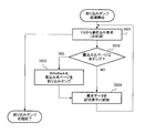
図18A、Bは、第4の実施の形態に係るメモリダンプ処理のフローチャートである。
先ず、情報処理装置101では、OSが実行されているものとする。
先ず、情報処理装置101では、OSが実行されているものとする。
ステップS701において、情報処理装置101のOSでクラッシュ事象、すなわち致命的なエラーが発生する。
ステップS702において、CPU111は、ダンプ処理を開始する。
以下、揮発性主記憶装置ダンプルーチン(ステップS703~S707)と不揮発性主記憶装置フラグ設定処理(ステップS708~S712)が並列に実行される。尚、揮発性主記憶装置ダンプルーチンと不揮発性主記憶装置フラグ設定処理は、直列に実行されても良いし、どちらが先に実行されてもよい。
以下、揮発性主記憶装置ダンプルーチン(ステップS703~S707)と不揮発性主記憶装置フラグ設定処理(ステップS708~S712)が並列に実行される。尚、揮発性主記憶装置ダンプルーチンと不揮発性主記憶装置フラグ設定処理は、直列に実行されても良いし、どちらが先に実行されてもよい。
ステップS703において、CPU111は、フォアグラウンドの揮発性主記憶装置ダンプルーチン(フォアグラウンドダンプ)を開始する。尚、フォアグラウンドとは、情報処理装置101が専らダンプ処理のために動作しており、業務が稼働していない状態を示す。
尚、CPU111は、主記憶装置(揮発性主記憶装置121および不揮発性主記憶装置131)のEEPROMを参照し、主記憶装置が揮発性か不揮発性か判別する。
ステップS704において、CPU111は、不揮発性主記憶装置131に揮発性主記憶装置121の全データまたは1部のデータをコピー可能な空き領域があるかチェックする。揮発性主記憶装置121のデータをコピー可能な空き領域がある場合、制御はステップS705に進み、揮発性主記憶装置121のデータをコピー可能な空き領域がない場合、制御はステップS706に進む。
ステップS705において、CPU111は、揮発性主記憶装置121のデータを不揮発性主記憶装置131にコピー(書き込み)する。発性主記憶装置121のデータを不揮発性主記憶装置131にコピーするときに、CPU111は、揮発性主記憶装置のもともとのメモリアドレスが後から判別可能なような付加情報(例えば、コピーしたデータの開始アドレスおよびサイズまたはアドレスのオフセットなど)を同時に保存する。
また、コピーの途中で不揮発性主記憶装置131の空き領域がなくなった場合は、制御はステップS706に進み、未コピーの揮発性主記憶装置121のデータは、外部記憶装置161にコピーされる。
ステップS706において、CPU111は、揮発性主記憶装置121のデータを外部記憶装置161にコピー(書き込み)する。
ステップS707において、CPU111は、揮発性主記憶装置ダンプルーチンを終了する。
尚、不揮発性主記憶装置131の空き領域は、あらかじめ予約されているように実装することも可能だし、揮発性主記憶装置ダンプルーチンは、クラッシュ事象発生時の状態により変化する空き領域に動的に対応できるよう実装されることが望ましい。
ステップS708において、CPU111は、不揮発性主記憶装置フラグ設定処理を開始する。
ステップS709において、CPU111は、BIOS設定情報173を参照し、不揮発性主記憶装置131がブロックアクセスであるかチェックする。不揮発性主記憶装置131がブロックアクセスの場合、制御はステップS710に進み、不揮発性主記憶装置131がブロックアクセスでない場合(バイトアクセスである場合)、制御はステップS711に進む。尚、上記チェックは、全ての不揮発性主記憶装置131に対して行う。
ステップS710において、CPU111は、ブロックアクセスである不揮発性主記憶装置131をダンプの対象外とする。
ステップS711において、CPU111は、バイトアクセスである不揮発性主記憶装置131のBGダンプフラグを設定する。詳細には、CPU111は、BIOS設定情報173を参照し、各不揮発性主記憶装置131の優先度(Pri)を確認する。CPU111は、Pri=Highである不揮発性主記憶装置131のBGダンプフラグを1、Pri=Lowである不揮発性主記憶装置131のBGダンプフラグを2に設定する。
BGダンプフラグが設定されたNVMコントローラ201は、記憶素子管理テーブル203のフラグを設定する。詳細には、NVMコントローラ201は、「使用領域(Dirty)」を「未ダンプ」に設定する。NVMコントローラ201は、「使用領域(Dirty)」以外のフラグを「空き領域」に設定する。
ステップS712において、CPU111は、不揮発性主記憶装置フラグ設定処理を終了する。
ステップS713において、CPU111は、不揮発性主記憶装置131の手動交換を行うか否か判断する。詳細には、CPU111は、BIOS設定情報173を参照し、「手動交換」がYかNかによって、揮発性主記憶装置131の手動交換を行うか否か判断する。手動交換を行う場合、制御はステップS714に進み、手動交換を行わない場合、制御はステップS717に進む。
ステップS714において、CPU111は、情報処理装置101の電源をオフにする。
また、CPU111は、ダンプ処理の開始および電源オフのタイミングそれぞれでBIOSから情報処理装置101を管理するBaseboard Management Controller(BMC)に対してイベント通知を行い、BMCは手動交換の準備および着手のタイミングをSimple Network Management Protocol(SNMP)トラップや電子メールなどの方法で保守員に知らせる。
ステップS715において、保守員が手動で不揮発性主記憶装置131を交換し、情報処理装置101の電源をオンにする。
保守員はその場またはサポートセンターに別途用意した計算機で取り外した不揮発性主記憶装置のデータをダンプし、外部記憶装置161にダンプされていたデータとマージすることで解析に必要なダンプデータを得る。
尚、セキュリティを考慮して不揮発性主記憶装置131のデータが暗号化されている場合、保守員は情報処理装置101の所有者の了承のもとに解読用コードを入手する。
ステップS716において、CPU111は、OSを起動する。
ステップS717において、CPU111は、不揮発性主記憶装置131のメモリアドレス空間が消えてしまわないよう、CPU111と揮発性主記憶装置121をリセットする。
ステップS717において、CPU111は、不揮発性主記憶装置131のメモリアドレス空間が消えてしまわないよう、CPU111と揮発性主記憶装置121をリセットする。
ステップS718において、CPU111は、OSを起動する。
ステップS719において、CPU111およびNVMコントローラ201は、BGダンプ処理を実行する。ステップS719では、例えば、図6のステップS507~S510の処理が実行される。尚、BGダンプ処理は、ステップS711においてBGダンプフラグが設定された不揮発性主記憶装置131で行われる。
ステップS719において、CPU111およびNVMコントローラ201は、BGダンプ処理を実行する。ステップS719では、例えば、図6のステップS507~S510の処理が実行される。尚、BGダンプ処理は、ステップS711においてBGダンプフラグが設定された不揮発性主記憶装置131で行われる。
ステップS720において、各NVMコントローラ201は、割り込みダンプ処理を行う。尚、割り込みダンプ処理は、図8または図14で説明した通りである。
尚、上述のCPU111が実行する各ステップは、CPU111がBIOS172を読み出して実行することにより実現される。
上記に様にして得られたダンプデータは取得タイミングやアドレスがバラバラのファイルとなってしまうため、別途用意するソフトウェアツールによりマージするか、バラバラのファイルを読み込み可能なダンプの解析ソフトを利用する。
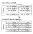
図19は、第4の実施の形態に係る各処理時のデータの位置を示す図である。
図19では、不揮発性主記憶装置131-1がブロックアクセス、不揮発性主記憶装置131-1がバイトアクセスとする。また、不揮発性主記憶装置131-3の記載は省略する。また、図19では、揮発性主記憶装置121-1を記載し、揮発性主記憶装置121-2、121-3は省略する。
図19では、不揮発性主記憶装置131-1がブロックアクセス、不揮発性主記憶装置131-1がバイトアクセスとする。また、不揮発性主記憶装置131-3の記載は省略する。また、図19では、揮発性主記憶装置121-1を記載し、揮発性主記憶装置121-2、121-3は省略する。
先ず、クラッシュ事象発生時には、不揮発性主記憶装置131-1はデータA、Bを格納している。不揮発性主記憶装置131-2はデータCを格納しており、空き領域(Free)を有する。揮発性主記憶装置121-1は、データD、Eを格納している(図19のクラッシュ事象発生時の状態)。尚、不揮発性主記憶装置131-1のデータA、Bは、バックグラウンドダンプ完了まで保持される。
揮発性主記憶装置ダンプルーチン(フォアグラウンドダンプ)が開始され、揮発性主記憶装置121-1のデータDは、不揮発性主記憶装置131-2にコピーされる(図19のフォアグラウンドダンプ中)。また、データDの、不揮発性主記憶装置131-2へのコピーにより、不揮発性主記憶装置131-2の空き領域は無くなる。
不揮発性主記憶装置131-2の空き領域が無いため、揮発性主記憶装置121-1のデータEは、外部記憶装置161にコピーされる(図19のフォアグラウンドダンプ完了)。
OSが再起動され(ステップS718)、BGダンプ処理が実行される(ステップS719)と、不揮発性主記憶装置131-2のデータC、Dは、外部記憶装置161にコピーされる。また、再起動されたOSのデータF、Gが揮発性主記憶装置121-1に書き込まれ、再起動されたOSのデータHが不揮発性主記憶装置131-2に書き込まれる(図19のバックグランドダンプ中)。
BGダンプ処理が終了すると、揮発性主記憶装置121-1は、データF、Gを格納しており、不揮発性主記憶装置131-2は、データHを格納しており、データDがあった領域は空き領域となっている(図19のバックグラウンドダンプ完了)。
第4の実施の形態の情報処理装置によれば、メモリダンプ処理による業務停止時間を短縮することができる。
第4の実施の形態の情報処理装置によれば、ブロックアクセスの不揮発性主記憶装置はダンプ不要であるから、これをダンプ対象外となるよう制御することで無駄な処理をなくすことができる。
第4の実施の形態の情報処理装置によれば、揮発性主記憶装置のデータを外部記憶装置よりも高速にアクセス可能な不揮発性主記憶の空き領域へコピーすることにより、フォアグラウンドのダンプの所要時間を短縮することができる。
第4の実施の形態の情報処理装置によれば、不揮発性主記憶装置から外部記憶装置へのダンプ処理をOS再起動後のバックグラウンド処理とすることで、業務停止時間を短縮することができる。
図20は、コンピュータシステムの構成図である。
以上説明したようなメモリダンプ処理は、当然一般的なコンピュータシステムによって実現することが可能である。図20において、実施の形態のメモリダンプ処理を実現するための情報処理装置11は、本体12とメモリ13とによって構成されている。メモリ13は、揮発性主記憶装置121、不揮発性主記憶装置131、外部記憶装置161、BIOS格納域171などの記憶装置に対応する。
以上説明したようなメモリダンプ処理は、当然一般的なコンピュータシステムによって実現することが可能である。図20において、実施の形態のメモリダンプ処理を実現するための情報処理装置11は、本体12とメモリ13とによって構成されている。メモリ13は、揮発性主記憶装置121、不揮発性主記憶装置131、外部記憶装置161、BIOS格納域171などの記憶装置に対応する。
このようなメモリ13に各実施の形態のメモリダンプ処理等を行うプログラムが格納され、そのプログラムが本体12によって実行されることによって、実施の形態の各種処理を実現することが可能となる。
このようなプログラムは、プログラム提供者側からネットワーク21を介して情報処理装置11にロードされることもできる。またプログラムは、市販され、流通している可搬型記憶媒体31に格納され、そのような可搬型記憶媒体31が情報処理装置11にセットされ、メモリ13に読み出されて本体12によって実行されることも可能である。
可搬型記憶媒体31としてはCD-ROM、フレキシブルディスク、光ディスク、光磁気ディスクなど様々な形式の記憶媒体を使用することができ、このような記憶媒体から読み出されたプログラムコード自体が実施の形態の機能を実現する。
Claims (10)
- オペレーティングシステムを実行する処理部と、
前記処理部が直接アクセス可能且つコントローラを有する不揮発性主記憶装置と、
前記処理部が直接アクセス可能でない外部記憶装置と、
を備え、
前記処理部が前記オペレーティングシステムのエラーを検出したとき、
前記処理部は、前記不揮発性主記憶装置以外をリセットして、前記オペレーティングシステムを再起動し、
前記コントローラは、前記不揮発性主記憶装置のデータを前記外部記憶装置に書き込むことを特徴とする情報処理装置。 - 前記不揮発性主記憶装置は、複数の不揮発性主記憶装置であり、
前記複数の不揮発性主記憶装置の各不揮発性主記憶装置の優先度が記載された設定情報を格納する情報格納部をさらに備え、
前記処理部は、前記設定情報を参照し、前記優先度の高い順に、前記不揮発性主記憶装置のデータを前記外部記憶装置に書き込む処理を前記コントローラに実行させることを特徴とする請求項1記載の情報処理装置。 - 前記コントローラは、
前記オペレーティングシステムから前記不揮発性主記憶装置へ書き込む第1のデータを受信し、
前記第1のデータが書き込まれる領域に存在する第2のデータが前記外部記憶装置に書き込まれていない場合、前記第2のデータを前記外部記憶装置に書き込み、
前記第2のデータを前記外部記憶装置に書き込み後、前記第1のデータを前記不揮発性主記憶装置へ書き込むことを特徴とする請求項1記載の情報処理装置。 - 前記不揮発性主記憶装置は、外部から見たアドレスに対して未割り当ての領域を有し、
前記コントローラは、
前記オペレーティングシステムから前記不揮発性主記憶装置へ書き込む第1のデータを受信し、
前記第1のデータが書き込まれる第1の領域に存在する第2のデータが前記外部記憶装置に書き込まれていない場合、
前記第1の領域に割り当てられている外部から見たアドレスを無効にし、
前記未割り当ての領域に前記第1の領域に割り当てられていた外部から見たアドレスを割り当て、
前記第1の領域に割り当てられていた外部から見たアドレスを割り当てた前記未割り当ての領域へ前記第1のデータを書き込むことを特徴とする請求項1記載の情報処理装置。 - 前記コントローラは、
前記不揮発性主記憶装置の複数の領域の各データが前記不揮発性主記憶装置へ書き込み済みであるかを示すフラグが記載された管理テーブルを有し、
前記オペレーティングシステムの動作時に、前記管理テーブルを参照し、前記外部記憶装置へ書き込んでいない未書込みデータを検出し、
該未書込みのデータを前記外部記憶装置へ書き込み、
書き込んだデータに対応するフラグを、前記外部記憶装置に書き込み済みであることを示すように設定することを特徴とする請求項1記載の情報処理装置。 - 前記処理部が前記オペレーティングシステムのエラーを検出したとき、
前記コントローラは、前記管理テーブルを参照し、前記フラグに基づいて、前記外部記憶装置へ書き込んでいない前記不揮発性主記憶装置のデータのみを前記外部記憶装置へ書き込むことを特徴とする請求項5記載の情報処理装置。 - 前記情報処理装置は、前記不揮発性主記憶装置がダンプ対象であるか否かを示す設定情報を格納する情報格納部をさらに備え、
前記不揮発性主記憶装置は、前記不揮発性主記憶装置のデータを前記外部記憶装置に書き込む処理を実行するか否かを示すダンプフラグを格納する主記憶装置情報格納部をさらに備え、
前記処理部は、前記設定情報に基づいて、ダンプ対象である前記不揮発性主記憶装置の前記ダンプフラグを有効に設定し、
前記コントローラは、前記ダンプフラグが有効の場合に、前記不揮発性主記憶装置のデータを前記外部記憶装置に書き込むことを特徴とする請求項1記載の情報処理装置。 - 前記処理部が直接アクセス可能な揮発性主記憶装置をさらに備え、
前記コントローラは、前記不揮発性主記憶装置のデータを前記外部記憶装置に書き込む前に、前記揮発性主記憶装置のデータを前記不揮発性主記憶装置に書き込むことを特徴とする請求項1記載の情報処理装置。 - オペレーティングシステムを実行する処理部と、前記処理部が直接アクセス可能な不揮発性主記憶装置と、前記処理部が直接アクセス可能でない外部記憶装置と、を備える情報処理装置が実行するメモリダンプ方法であって、
前記オペレーティングシステムのエラーを検出し、
前記不揮発性主記憶装置以外をリセットし、
前記オペレーティングシステムを再起動し、
前記不揮発性主記憶装置のデータを前記外部記憶装置に書き込む
処理を備えるメモリダンプ方法。 - オペレーティングシステムを実行する処理部と、前記処理部が直接アクセス可能な不揮発性主記憶装置と、前記処理部が直接アクセス可能でない外部記憶装置と、を備えるコンピュータに、
前記オペレーティングシステムのエラーを検出し、
前記不揮発性主記憶装置以外をリセットし、
前記オペレーティングシステムを再起動し、
前記不揮発性主記憶装置のデータを前記外部記憶装置に書き込む
処理を実行させるメモリダンププログラム。
Priority Applications (4)
| Application Number | Priority Date | Filing Date | Title |
|---|---|---|---|
| JP2015529269A JP6094677B2 (ja) | 2013-07-31 | 2013-07-31 | 情報処理装置、メモリダンプ方法、およびメモリダンププログラム |
| EP13890813.2A EP3029572A4 (en) | 2013-07-31 | 2013-07-31 | INFORMATION PROCESSING DEVICE, MEMORY STORAGE METHOD AND STORAGE STORAGE PROGRAM |
| PCT/JP2013/070698 WO2015015589A1 (ja) | 2013-07-31 | 2013-07-31 | 情報処理装置、メモリダンプ方法、およびメモリダンププログラム |
| US15/003,892 US10025670B2 (en) | 2013-07-31 | 2016-01-22 | Information processing apparatus, memory dump method, and storage medium |
Applications Claiming Priority (1)
| Application Number | Priority Date | Filing Date | Title |
|---|---|---|---|
| PCT/JP2013/070698 WO2015015589A1 (ja) | 2013-07-31 | 2013-07-31 | 情報処理装置、メモリダンプ方法、およびメモリダンププログラム |
Related Child Applications (1)
| Application Number | Title | Priority Date | Filing Date |
|---|---|---|---|
| US15/003,892 Continuation US10025670B2 (en) | 2013-07-31 | 2016-01-22 | Information processing apparatus, memory dump method, and storage medium |
Publications (1)
| Publication Number | Publication Date |
|---|---|
| WO2015015589A1 true WO2015015589A1 (ja) | 2015-02-05 |
Family
ID=52431169
Family Applications (1)
| Application Number | Title | Priority Date | Filing Date |
|---|---|---|---|
| PCT/JP2013/070698 Ceased WO2015015589A1 (ja) | 2013-07-31 | 2013-07-31 | 情報処理装置、メモリダンプ方法、およびメモリダンププログラム |
Country Status (4)
| Country | Link |
|---|---|
| US (1) | US10025670B2 (ja) |
| EP (1) | EP3029572A4 (ja) |
| JP (1) | JP6094677B2 (ja) |
| WO (1) | WO2015015589A1 (ja) |
Cited By (1)
| Publication number | Priority date | Publication date | Assignee | Title |
|---|---|---|---|---|
| WO2016139774A1 (ja) * | 2015-03-04 | 2016-09-09 | 富士通株式会社 | 情報処理装置、情報処理システム |
Families Citing this family (7)
| Publication number | Priority date | Publication date | Assignee | Title |
|---|---|---|---|---|
| CN104335220B (zh) * | 2012-03-30 | 2018-04-20 | 爱迪德技术有限公司 | 用于防止和检测安全威胁的方法和系统 |
| CN106959906B (zh) * | 2017-03-28 | 2020-06-23 | 联想(北京)有限公司 | 信息处理方法、信息处理装置及电子设备 |
| US10387261B2 (en) * | 2017-05-05 | 2019-08-20 | Dell Products L.P. | System and method to capture stored data following system crash |
| US11119875B2 (en) | 2017-06-16 | 2021-09-14 | Hewlett-Packard Development Company, L.P. | Communication port recovery |
| US10705902B2 (en) | 2018-05-03 | 2020-07-07 | Western Digital Technologies, Inc. | Crash log storage and retrieval using boot partitions in solid state systems |
| US11487601B2 (en) * | 2020-03-26 | 2022-11-01 | Arista Networks, Inc. | Persistent crash logging |
| CN111737171B (zh) * | 2020-05-29 | 2022-04-19 | 苏州浪潮智能科技有限公司 | 一种交换机光模块信息获取系统、方法、设备及存储介质 |
Citations (10)
| Publication number | Priority date | Publication date | Assignee | Title |
|---|---|---|---|---|
| JPH04182748A (ja) | 1990-11-16 | 1992-06-30 | Nec Eng Ltd | メモリダンプ装置 |
| JPH05134906A (ja) * | 1991-11-11 | 1993-06-01 | Nec Corp | メモリ情報収集方式 |
| JPH09259014A (ja) * | 1996-03-25 | 1997-10-03 | Meidensha Corp | 異常情報記録方式 |
| JPH10333944A (ja) | 1997-05-30 | 1998-12-18 | Nec Software Ltd | メモリダンプ採取方式 |
| JP2004102395A (ja) | 2002-09-05 | 2004-04-02 | Hitachi Ltd | メモリダンプデータの取得方法および情報処理装置、ならびにそのプログラム |
| JP2004362426A (ja) * | 2003-06-06 | 2004-12-24 | Sony Corp | 情報処理システム及びその制御方法、並びにコンピュータ・プログラム |
| US20050204107A1 (en) * | 2004-03-13 | 2005-09-15 | Hewlett-Packard Development Company, L.P. | Method and apparatus for dumping memory |
| JP2008242999A (ja) * | 2007-03-28 | 2008-10-09 | Hitachi Ltd | 情報処理装置およびメモリダンプ方法 |
| JP2009205254A (ja) * | 2008-02-26 | 2009-09-10 | Fujitsu Ltd | 計算機、ダンププログラムおよびダンプ方法 |
| JP2011257987A (ja) * | 2010-06-09 | 2011-12-22 | Mitsubishi Electric Corp | 計算機システム |
Family Cites Families (13)
| Publication number | Priority date | Publication date | Assignee | Title |
|---|---|---|---|---|
| US5111384A (en) * | 1990-02-16 | 1992-05-05 | Bull Hn Information Systems Inc. | System for performing dump analysis |
| JPH03257641A (ja) * | 1990-03-08 | 1991-11-18 | Nec Corp | メモリダンプ採取方式 |
| JP2002073378A (ja) * | 2000-09-04 | 2002-03-12 | Hitachi Ltd | 計算機システムのダンプ取得方法および装置 |
| US6779132B2 (en) * | 2001-08-31 | 2004-08-17 | Bull Hn Information Systems Inc. | Preserving dump capability after a fault-on-fault or related type failure in a fault tolerant computer system |
| US7831857B2 (en) * | 2006-10-31 | 2010-11-09 | Hewlett-Packard Development Company, L.P. | Method and system for recovering from operating system crash or failure |
| WO2008114395A1 (ja) * | 2007-03-19 | 2008-09-25 | Fujitsu Limited | 仮想計算機ダンプ採取プログラム、ダンプ採取システムおよびダンプ採取方法 |
| DE102008040486A1 (de) | 2008-07-17 | 2010-01-21 | Evonik Goldschmidt Gmbh | Verwendung von ionischen Flüssigkeiten als Zusatzstoff für Reinigungsverfahren in verflüssigtem und/oder überkritischem Gas |
| JP5120664B2 (ja) * | 2009-07-06 | 2013-01-16 | 日本電気株式会社 | サーバシステム及びクラッシュダンプ採取方法 |
| US8601323B2 (en) * | 2010-12-13 | 2013-12-03 | Sap Ag | Advanced management of runtime errors |
| EP2660724B1 (en) * | 2010-12-27 | 2020-07-29 | Fujitsu Limited | Information processing device having memory dump function, memory dump method, and memory dump program |
| US8762790B2 (en) * | 2011-09-07 | 2014-06-24 | International Business Machines Corporation | Enhanced dump data collection from hardware fail modes |
| US9740551B2 (en) * | 2014-12-02 | 2017-08-22 | International Business Machines Corporation | Enhanced restart of a core dumping application |
| US10002040B2 (en) * | 2016-01-04 | 2018-06-19 | International Business Machines Corporation | Detection and automatic transfer of standalone system dumps |
-
2013
- 2013-07-31 JP JP2015529269A patent/JP6094677B2/ja active Active
- 2013-07-31 WO PCT/JP2013/070698 patent/WO2015015589A1/ja not_active Ceased
- 2013-07-31 EP EP13890813.2A patent/EP3029572A4/en not_active Withdrawn
-
2016
- 2016-01-22 US US15/003,892 patent/US10025670B2/en active Active
Patent Citations (10)
| Publication number | Priority date | Publication date | Assignee | Title |
|---|---|---|---|---|
| JPH04182748A (ja) | 1990-11-16 | 1992-06-30 | Nec Eng Ltd | メモリダンプ装置 |
| JPH05134906A (ja) * | 1991-11-11 | 1993-06-01 | Nec Corp | メモリ情報収集方式 |
| JPH09259014A (ja) * | 1996-03-25 | 1997-10-03 | Meidensha Corp | 異常情報記録方式 |
| JPH10333944A (ja) | 1997-05-30 | 1998-12-18 | Nec Software Ltd | メモリダンプ採取方式 |
| JP2004102395A (ja) | 2002-09-05 | 2004-04-02 | Hitachi Ltd | メモリダンプデータの取得方法および情報処理装置、ならびにそのプログラム |
| JP2004362426A (ja) * | 2003-06-06 | 2004-12-24 | Sony Corp | 情報処理システム及びその制御方法、並びにコンピュータ・プログラム |
| US20050204107A1 (en) * | 2004-03-13 | 2005-09-15 | Hewlett-Packard Development Company, L.P. | Method and apparatus for dumping memory |
| JP2008242999A (ja) * | 2007-03-28 | 2008-10-09 | Hitachi Ltd | 情報処理装置およびメモリダンプ方法 |
| JP2009205254A (ja) * | 2008-02-26 | 2009-09-10 | Fujitsu Ltd | 計算機、ダンププログラムおよびダンプ方法 |
| JP2011257987A (ja) * | 2010-06-09 | 2011-12-22 | Mitsubishi Electric Corp | 計算機システム |
Non-Patent Citations (1)
| Title |
|---|
| See also references of EP3029572A4 |
Cited By (1)
| Publication number | Priority date | Publication date | Assignee | Title |
|---|---|---|---|---|
| WO2016139774A1 (ja) * | 2015-03-04 | 2016-09-09 | 富士通株式会社 | 情報処理装置、情報処理システム |
Also Published As
| Publication number | Publication date |
|---|---|
| JP6094677B2 (ja) | 2017-03-15 |
| US10025670B2 (en) | 2018-07-17 |
| EP3029572A1 (en) | 2016-06-08 |
| US20160139995A1 (en) | 2016-05-19 |
| EP3029572A4 (en) | 2016-07-20 |
| JPWO2015015589A1 (ja) | 2017-03-02 |
Similar Documents
| Publication | Publication Date | Title |
|---|---|---|
| JP6094677B2 (ja) | 情報処理装置、メモリダンプ方法、およびメモリダンププログラム | |
| JP6517684B2 (ja) | メモリシステムおよび制御方法 | |
| JP6517685B2 (ja) | メモリシステムおよび制御方法 | |
| US8447918B2 (en) | Garbage collection for failure prediction and repartitioning | |
| US9489258B2 (en) | Green NAND SSD application and driver | |
| JP5937697B2 (ja) | ストレージシステム | |
| JP5376983B2 (ja) | メモリシステム | |
| US9081690B2 (en) | Storage system and management method of control information therein | |
| US9274942B2 (en) | Information processing system and nonvolatile storage unit | |
| US20150331624A1 (en) | Host-controlled flash translation layer snapshot | |
| JP4961319B2 (ja) | 仮想ボリュームにおける仮想領域に動的に実領域を割り当てるストレージシステム | |
| US10310764B2 (en) | Semiconductor memory device and storage apparatus comprising semiconductor memory device | |
| US11194481B2 (en) | Information processing apparatus and method for controlling information processing apparatus | |
| JP2008015769A (ja) | ストレージシステム及び書き込み分散方法 | |
| US10664193B2 (en) | Storage system for improved efficiency of parity generation and minimized processor load | |
| KR20230040057A (ko) | 시스템의 읽기 성능을 개선하기 위한 장치 및 방법 | |
| KR101596833B1 (ko) | 플래시 메모리를 기반으로 하는 저장 장치 및 그것을 포함한 사용자 장치 | |
| CN105404468B (zh) | 绿能与非固态硬盘应用及其驱动器 | |
| JP2015053075A (ja) | メモリシステム、情報処理装置および記憶装置 | |
| US20110264848A1 (en) | Data recording device | |
| JP6666405B2 (ja) | メモリシステムおよび制御方法 | |
| JP6163588B2 (ja) | ストレージシステム | |
| CN111752475A (zh) | 在存储服务器中进行数据存取管理的方法与装置 | |
| HK1220271B (zh) | 绿能与非固态硬盘应用及其驱动器 |
Legal Events
| Date | Code | Title | Description |
|---|---|---|---|
| 121 | Ep: the epo has been informed by wipo that ep was designated in this application |
Ref document number: 13890813 Country of ref document: EP Kind code of ref document: A1 |
|
| ENP | Entry into the national phase |
Ref document number: 2015529269 Country of ref document: JP Kind code of ref document: A |
|
| WWE | Wipo information: entry into national phase |
Ref document number: 2013890813 Country of ref document: EP |
|
| NENP | Non-entry into the national phase |
Ref country code: DE |