WO2015016153A1 - Cu-Ga合金スパッタリングターゲット及びその製造方法 - Google Patents
Cu-Ga合金スパッタリングターゲット及びその製造方法 Download PDFInfo
- Publication number
- WO2015016153A1 WO2015016153A1 PCT/JP2014/069735 JP2014069735W WO2015016153A1 WO 2015016153 A1 WO2015016153 A1 WO 2015016153A1 JP 2014069735 W JP2014069735 W JP 2014069735W WO 2015016153 A1 WO2015016153 A1 WO 2015016153A1
- Authority
- WO
- WIPO (PCT)
- Prior art keywords
- phase
- sputtering target
- compound
- alloy
- less
- Prior art date
- Legal status (The legal status is an assumption and is not a legal conclusion. Google has not performed a legal analysis and makes no representation as to the accuracy of the status listed.)
- Ceased
Links
Images


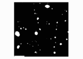
Classifications
-
- C—CHEMISTRY; METALLURGY
- C23—COATING METALLIC MATERIAL; COATING MATERIAL WITH METALLIC MATERIAL; CHEMICAL SURFACE TREATMENT; DIFFUSION TREATMENT OF METALLIC MATERIAL; COATING BY VACUUM EVAPORATION, BY SPUTTERING, BY ION IMPLANTATION OR BY CHEMICAL VAPOUR DEPOSITION, IN GENERAL; INHIBITING CORROSION OF METALLIC MATERIAL OR INCRUSTATION IN GENERAL
- C23C—COATING METALLIC MATERIAL; COATING MATERIAL WITH METALLIC MATERIAL; SURFACE TREATMENT OF METALLIC MATERIAL BY DIFFUSION INTO THE SURFACE, BY CHEMICAL CONVERSION OR SUBSTITUTION; COATING BY VACUUM EVAPORATION, BY SPUTTERING, BY ION IMPLANTATION OR BY CHEMICAL VAPOUR DEPOSITION, IN GENERAL
- C23C14/00—Coating by vacuum evaporation, by sputtering or by ion implantation of the coating forming material
- C23C14/22—Coating by vacuum evaporation, by sputtering or by ion implantation of the coating forming material characterised by the process of coating
- C23C14/34—Sputtering
- C23C14/3407—Cathode assembly for sputtering apparatus, e.g. Target
- C23C14/3414—Metallurgical or chemical aspects of target preparation, e.g. casting, powder metallurgy
-
- B—PERFORMING OPERATIONS; TRANSPORTING
- B22—CASTING; POWDER METALLURGY
- B22F—WORKING METALLIC POWDER; MANUFACTURE OF ARTICLES FROM METALLIC POWDER; MAKING METALLIC POWDER; APPARATUS OR DEVICES SPECIALLY ADAPTED FOR METALLIC POWDER
- B22F3/00—Manufacture of workpieces or articles from metallic powder characterised by the manner of compacting or sintering; Apparatus specially adapted therefor ; Presses and furnaces
- B22F3/12—Both compacting and sintering
- B22F3/16—Both compacting and sintering in successive or repeated steps
-
- B—PERFORMING OPERATIONS; TRANSPORTING
- B22—CASTING; POWDER METALLURGY
- B22F—WORKING METALLIC POWDER; MANUFACTURE OF ARTICLES FROM METALLIC POWDER; MAKING METALLIC POWDER; APPARATUS OR DEVICES SPECIALLY ADAPTED FOR METALLIC POWDER
- B22F5/00—Manufacture of workpieces or articles from metallic powder characterised by the special shape of the product
-
- C—CHEMISTRY; METALLURGY
- C22—METALLURGY; FERROUS OR NON-FERROUS ALLOYS; TREATMENT OF ALLOYS OR NON-FERROUS METALS
- C22C—ALLOYS
- C22C9/00—Alloys based on copper
-
- C—CHEMISTRY; METALLURGY
- C23—COATING METALLIC MATERIAL; COATING MATERIAL WITH METALLIC MATERIAL; CHEMICAL SURFACE TREATMENT; DIFFUSION TREATMENT OF METALLIC MATERIAL; COATING BY VACUUM EVAPORATION, BY SPUTTERING, BY ION IMPLANTATION OR BY CHEMICAL VAPOUR DEPOSITION, IN GENERAL; INHIBITING CORROSION OF METALLIC MATERIAL OR INCRUSTATION IN GENERAL
- C23C—COATING METALLIC MATERIAL; COATING MATERIAL WITH METALLIC MATERIAL; SURFACE TREATMENT OF METALLIC MATERIAL BY DIFFUSION INTO THE SURFACE, BY CHEMICAL CONVERSION OR SUBSTITUTION; COATING BY VACUUM EVAPORATION, BY SPUTTERING, BY ION IMPLANTATION OR BY CHEMICAL VAPOUR DEPOSITION, IN GENERAL
- C23C14/00—Coating by vacuum evaporation, by sputtering or by ion implantation of the coating forming material
- C23C14/06—Coating by vacuum evaporation, by sputtering or by ion implantation of the coating forming material characterised by the coating material
- C23C14/14—Metallic material, boron or silicon
-
- H—ELECTRICITY
- H01—ELECTRIC ELEMENTS
- H01J—ELECTRIC DISCHARGE TUBES OR DISCHARGE LAMPS
- H01J37/00—Discharge tubes with provision for introducing objects or material to be exposed to the discharge, e.g. for the purpose of examination or processing thereof
- H01J37/32—Gas-filled discharge tubes
- H01J37/34—Gas-filled discharge tubes operating with cathodic sputtering
- H01J37/3411—Constructional aspects of the reactor
- H01J37/3414—Targets
- H01J37/3426—Material
- H01J37/3429—Plural materials
-
- B—PERFORMING OPERATIONS; TRANSPORTING
- B22—CASTING; POWDER METALLURGY
- B22F—WORKING METALLIC POWDER; MANUFACTURE OF ARTICLES FROM METALLIC POWDER; MAKING METALLIC POWDER; APPARATUS OR DEVICES SPECIALLY ADAPTED FOR METALLIC POWDER
- B22F2201/00—Treatment under specific atmosphere
- B22F2201/01—Reducing atmosphere
-
- B—PERFORMING OPERATIONS; TRANSPORTING
- B22—CASTING; POWDER METALLURGY
- B22F—WORKING METALLIC POWDER; MANUFACTURE OF ARTICLES FROM METALLIC POWDER; MAKING METALLIC POWDER; APPARATUS OR DEVICES SPECIALLY ADAPTED FOR METALLIC POWDER
- B22F2301/00—Metallic composition of the powder or its coating
- B22F2301/10—Copper
-
- B—PERFORMING OPERATIONS; TRANSPORTING
- B22—CASTING; POWDER METALLURGY
- B22F—WORKING METALLIC POWDER; MANUFACTURE OF ARTICLES FROM METALLIC POWDER; MAKING METALLIC POWDER; APPARATUS OR DEVICES SPECIALLY ADAPTED FOR METALLIC POWDER
- B22F2302/00—Metal Compound, non-Metallic compound or non-metal composition of the powder or its coating
- B22F2302/45—Others, including non-metals
-
- B—PERFORMING OPERATIONS; TRANSPORTING
- B22—CASTING; POWDER METALLURGY
- B22F—WORKING METALLIC POWDER; MANUFACTURE OF ARTICLES FROM METALLIC POWDER; MAKING METALLIC POWDER; APPARATUS OR DEVICES SPECIALLY ADAPTED FOR METALLIC POWDER
- B22F2303/00—Functional details of metal or compound in the powder or product
- B22F2303/01—Main component
-
- B—PERFORMING OPERATIONS; TRANSPORTING
- B22—CASTING; POWDER METALLURGY
- B22F—WORKING METALLIC POWDER; MANUFACTURE OF ARTICLES FROM METALLIC POWDER; MAKING METALLIC POWDER; APPARATUS OR DEVICES SPECIALLY ADAPTED FOR METALLIC POWDER
- B22F2303/00—Functional details of metal or compound in the powder or product
- B22F2303/15—Intermetallic
-
- B—PERFORMING OPERATIONS; TRANSPORTING
- B22—CASTING; POWDER METALLURGY
- B22F—WORKING METALLIC POWDER; MANUFACTURE OF ARTICLES FROM METALLIC POWDER; MAKING METALLIC POWDER; APPARATUS OR DEVICES SPECIALLY ADAPTED FOR METALLIC POWDER
- B22F2304/00—Physical aspects of the powder
- B22F2304/10—Micron size particles, i.e. above 1 micrometer up to 500 micrometer
Definitions
- the present invention relates to a Cu—Ga alloy sputtering target used for forming a Cu—In—Ga—Se compound film (hereinafter abbreviated as CIGS film) for forming a light absorption layer of a CIGS thin film solar cell. And a manufacturing method thereof.
- CIGS film Cu—In—Ga—Se compound film
- This application claims priority on August 1, 2013 based on Japanese Patent Application No. 2013-160134 filed in Japan, the contents of which are incorporated herein by reference.
- thin film solar cells based on chalcopyrite compound semiconductors have come into practical use, and thin film solar cells based on this compound semiconductor form a Mo electrode layer serving as a positive electrode on a soda-lime glass substrate.
- a light absorption layer made of a CIGS film is formed on the Mo electrode layer, a buffer layer made of ZnS, CdS, or the like is formed on the light absorption layer, and a transparent electrode layer serving as a negative electrode is formed on the buffer layer. It has a basic structure formed.
- a method for forming the light absorption layer for example, a method of forming a film by a multi-source deposition method is known.
- the light absorption layer obtained by this method can obtain high energy conversion efficiency, but the uniformity of the film thickness distribution tends to decrease when the film is formed on a large-area substrate due to vapor deposition from a point source. . Therefore, a method for forming a light absorption layer by a sputtering method has been proposed.
- an In film is formed by sputtering using an In target, and a Cu—Ga binary alloy sputtering target is used on the In film.
- a Cu—Ga binary alloy film was formed by sputtering, and then the obtained precursor film made of the In film and the Cu—Ga binary alloy film was heat-treated in an Se atmosphere to form a CIGS film.
- a forming method (selenization method) is employed.
- the Cu—Ga alloy film and the In film laminated precursor film are formed from the metal back electrode layer side with a high Ga content Cu—Ga alloy layer and a low Ga content Cu—Ga alloy.
- a layer and an In layer are formed by a sputtering method in this order, and this is heat-treated in a selenium and / or sulfur atmosphere, so that the inside of the thin-film light absorption layer from the interface layer (buffer layer) side to the metal back electrode layer side.
- the Ga content in the Cu—Ga alloy sputtering target is 1 to 40 atomic% (Patent Document 1).
- a Cu—Ga alloy fired sputtering target in which Cu—Ga mixed fine powder produced by a water atomizer is sintered by hot pressing is proposed.
- Patent Document 2 This Cu—Ga alloy fired body sputtering target has a single composition and has a peak intensity other than the main peak ( ⁇ phase: Cu 9 Ga 4 phase) in the graph obtained by X-ray diffraction of the Cu—Ga alloy. It is 5% or less with respect to the peak, and the average crystal grain size is 5 to 30 ⁇ m. In addition, this target has an oxygen content of 350 to 400 ppm.
- Non-patent Document 1 In order to improve the power generation efficiency of the light absorption layer made of the CIGS film, it is effective to add Na to the light absorption layer by diffusion from the alkaline glass substrate (Non-patent Document 1).
- Non-patent Document 1 In the case of a flexible CIGS solar cell based on a polymer film or the like instead of alkaline glass, there is an inconvenience that the supply source of Na is lost because there is no alkaline glass substrate.
- Non-Patent Document 1 a method of forming soda-lime glass between the Mo electrode layer and the substrate has been proposed (Non-Patent Document 1).
- CIG Cu—In—Ga
- the conventional techniques described above have the following problems.
- the Cu—Ga alloy sputtering target is produced by hot pressing, whereby the oxygen content is reduced and abnormal discharge during sputtering is reduced. From the viewpoint of battery production, a sputtering target having a lower oxygen content is desired. Further, as disclosed in Patent Document 2, the sputtering target produced by the melting method can greatly reduce the oxygen content to 40 to 50 ppm, but the average particle size becomes very large as 830 to 1100 ⁇ m, which is abnormal. There is a disadvantage that discharge increases.
- the present invention has been made in view of the above-described problems, and it is possible to further reduce the oxygen content of a sputtering target of a Cu—Ga fired body, and to perform abnormal discharge while containing a high concentration of Na. It is an object of the present invention to provide a sputtering target of a Cu—Ga fired body that suppresses the above and a method for manufacturing the same.
- the present invention has the following aspects.
- (1) A structure in which a Na compound phase is dispersed in a substrate having a ⁇ phase and a ⁇ phase of a Cu—Ga alloy, and contains Ga: 20 to 30 atomic%, Na: 0.05 to 10 atomic%.
- the balance is a fired body having a composition composed of Cu and inevitable impurities (including elements other than Na in the Na compound), wherein the average particle diameter of the ⁇ phase is 30 to 100 ⁇ m, and the Na compound phase A Cu—Ga alloy sputtering target having an average particle diameter of 8.5 ⁇ m or less.
- the main peak intensity of X-ray diffraction attributed to the ⁇ phase is 5% or more of the main peak intensity of X-ray diffraction attributed to the ⁇ phase, (1) or (2) Cu-Ga alloy sputtering target.
- the ⁇ phase and ⁇ phase in the present invention are the ⁇ phase (chemical formula: Cu 9 Ga 4 ) and ⁇ phase (chemical formula: Cu 3 Ga) in the phase diagram related to the Cu—Ga alloy shown in FIG. Each corresponds.
- Na was added to the CIG alloy.
- Na is added to the Cu—Ga alloy in the form of a compound instead of Na alone, and the coarsening of the Na compound phase is suppressed, and the oxygen content in the sputtering target is limited.
- a sputtering target containing Na but suppressing abnormal discharge was realized.
- the reason why the Na content contained in the state of the Na compound is set within the above range is that when the Na content exceeds 10 atomic%, a sufficient sintering density cannot be ensured and at the same time during sputtering. This is because the abnormal discharge increases. On the other hand, if the Na content is less than 0.05 atomic%, the Na content in the film is insufficient, and the intended addition of Na cannot be achieved.
- the fired body of the Cu—Ga alloy sputtering target according to the present invention is a metal substrate in which a ⁇ phase and a ⁇ phase coexist, and the average particle size of the ⁇ phase in the substrate is 30 to 100 ⁇ m. It has a structure in which the Na compound phase is dispersed, and the average particle size of the Na compound phase is 8.5 ⁇ m or less. Considering the production cost of the sputtering target and the effect to be obtained, the preferable lower limit of the average particle diameter of the Na compound phase is 5.0 ⁇ m, but is not limited thereto.
- the average particle diameter is a projected area equivalent circle diameter.
- a sputtering target containing a Na compound contains a Na compound that is an insulator, if the Na compound phase is not properly dispersed, abnormal discharge is likely to occur during sputtering.
- the present inventors have found that when the average particle size of the Na compound is 8.5 ⁇ m or less, abnormal discharge due to the Na compound is significantly reduced.
- the sputtering target of the present invention by optimizing the average particle diameter of the Na compound phase as described above, high-speed film formation by sputtering is possible. That is, in the sputtering target of the present invention, by setting the average particle diameter of each Na compound phase to 8.5 ⁇ m or less, abnormal discharge due to the Na compound is suppressed, and stable sputtering becomes possible.
- the size of the Na compound phase dispersed in the sputtering target is preferably as small as possible, and the size is set to an average particle size of 8.5 ⁇ m or less, but the maximum particle size is also set to 20 ⁇ m or less. Is preferred. Considering the production cost of the sputtering target and the effect obtained, the preferred minimum particle size is 0.5 ⁇ m, but is not limited to this.
- the Cu—Ga alloy sputtering target according to the present invention preferably has an oxygen content of 200 mass ppm or less.
- oxygen and the Na compound may react to form highly hygroscopic NaO.
- oxygen content exceeds 200 mass ppm, there is a high possibility that abnormal discharge occurs in the sputtering target, so the oxygen content was set to 200 mass ppm or less.
- the preferable lower limit of the oxygen content is 50 mass ppm, but is not limited thereto.
- the average particle diameter of the ⁇ phase in the metal substrate is 30 to 100 ⁇ m, a coarse Na compound phase is generated even if the Na compound is contained. Not. In addition, when the average particle diameter of the ⁇ phase exceeds 100 ⁇ m, the Na compound phase tends to be coarsened, which is not preferable. Further, if the average particle size of the ⁇ phase is less than 30 ⁇ m, the oxygen content tends to exceed 200 ppm by mass, which is not preferable.
- the ⁇ phase and the ⁇ phase coexist in the metal substrate, the average particle size of the ⁇ phase is 30 to 100 ⁇ m, and the average particle size is 8 Since the Na compound phase of .5 ⁇ m or less is finely dispersed and the oxygen content is 200 mass ppm or less, the oxygen content is low and the particle size is small, so that abnormal discharge is greatly reduced.
- the reason why the Ga content is 20 atomic% or more is that when it is less than 20 atomic%, the average particle size of the ⁇ phase decreases and the oxygen content tends to increase.
- the reason why the Ga content is 30 atomic% or less is that if it exceeds 30 atomic%, the proportion of the ⁇ phase decreases, the average particle diameter of the ⁇ phase increases, and a coarse Na compound phase is generated. It is because it becomes easy to be done.
- the Na compound, NaF, Na 2 S it is possible to use at least one or more of Na 2 Se and Na 3 AlF 6.
- elements F, S, Se, and Al other than Na in the Na compound were treated as impurities in the target composition and included in inevitable impurities.
- the method for producing a Cu—Ga alloy sputtering target according to the present invention is a method for producing the above-described Cu—Ga alloy sputtering target according to the present invention, and comprises pure Cu powder, Cu—Ga alloy powder and Na compound. It has the process which heats the molded object which consists of mixed powder in a reducing atmosphere, and carries out an atmospheric pressure sintering. That is, in this sputtering target manufacturing method, a compact made of pure Cu powder, Cu—Ga alloy powder and Na compound is heated in a reducing atmosphere and sintered at normal pressure.
- ⁇ phase and ⁇ phase appear as metal phases in the fired body, X-ray diffraction peak attributed to ⁇ phase of Cu—Ga alloy and X-ray diffraction attributed to ⁇ phase A fired body in which a peak is observed can be obtained with a very low oxygen content.
- pure Cu powder that is easily plastically deformed as a raw material facilitates shape retention when forming a molded body.
- pure Cu powder is oxidized in the air at room temperature, since it is easily reduced by heating in a reducing atmosphere, it does not cause an increase in the oxygen content.
- a Cu—Ga alloy powder of 50 atomic% Ga a liquid phase is generated during sintering, and a high-density fired body can be obtained.
- the present invention has the following effects. That is, according to the Cu—Ga alloy sputtering target and the manufacturing method thereof according to the present invention, the main peak intensity of the X-ray diffraction peak attributed to the ⁇ phase is 5% of the main peak intensity of the X-ray diffraction peak attributed to the ⁇ phase.
- the ⁇ phase and the ⁇ phase coexist in the fired body, and the average particle diameter of the ⁇ phase is as small as 30 to 100 ⁇ m.
- the Na compound phase has an average particle diameter of 8
- the oxygen content is low and the particle size is small because the oxygen content is 200 mass ppm or less, and the abnormal discharge is greatly reduced.
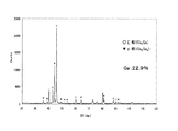
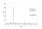
- a Cu—Ga alloy system phase diagram is shown. It is a graph which shows the diffraction peak measured by X-ray diffraction about the sputtering target of Example 2 containing 22.9 atomic% of Ga. It is a graph which shows the diffraction peak measured by X-ray diffraction about the sputtering target of Example 4 which contains 29.1 atomic% of Ga. It is a graph which shows the diffraction peak measured by X-ray diffraction about the sputtering target of the comparative example 4 containing 30.4 atomic% of Ga.
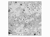
- composition image acquired by the electron beam microanalyzer (EPMA) about the sputtering target of Example 2 which contains 22.9 atomic% of Ga.
- EPMA electron beam microanalyzer
- element distribution mapping image of Ga acquired by EPMA about the sputtering target of Example 2 containing 22.9 atomic% of Ga.
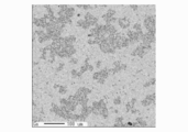
- element distribution mapping image of Na acquired by EPMA about the sputtering target of Example 2 containing 22.9 atomic% of Ga.
- the sputtering target of this embodiment contains Ga: 20 to 30 atomic%, Na: 0.05 to 10 atomic%, and the balance is composed of Cu and inevitable impurities (including elements other than Na in the Na compound).
- the ⁇ phase (Cu 9 Ga 4 phase) and the ⁇ phase (Cu 3 Ga phase) of the Cu—Ga alloy existed, and the Na compound phase was dispersed. It has a texture, the ⁇ phase has an average particle size of 30 to 100 ⁇ m, the Na compound phase has an average particle size of 8.5 ⁇ m or less, and its maximum particle size is 20 ⁇ m or less.
- the oxygen content of the fired body is 200 ppm by mass or less.
- this sputtering target has a crystal structure in which a ⁇ phase (Ga-rich region: Cu 9 Ga 4 phase) containing a relatively large amount of Ga in the fired body is dispersed.
- the Ga-rich region is, for example, a region observed in white in a COMPO image by EPMA as shown in FIG.
- the average particle diameter of the ⁇ phase is such that the surface of the sample cut out from the sputtering target is mirror-polished and etched with an etching solution composed of nitric acid and pure water, and then the grain boundary can be determined: 50 Take a micrograph with an optical microscope within the range of up to 1000 times, draw 10 straight lines that divide one side of the obtained photo into 11 equal parts, count the crystal grains that pass through these 10 straight lines, and It calculated
- required using the calculation formula. Average grain size (value obtained by correcting the length of 10 line segments on the photograph to the actual length) / (number of crystal grains through which 10 line segments pass)
- the average particle diameter of the Na compound phase was measured based on an element distribution mapping image of Na obtained by EPMA as shown in FIG.
- region has shown the presence of Na and represents the magnitude
- oxygen content was measured by an infrared absorption method described in JIS Z 2613 “General Rules for Determination of Oxygen of Metallic Materials”.
- the method for producing the sputtering target of the present embodiment includes a step of heating a molded body made of a mixed powder of pure Cu powder, Cu—Ga alloy powder and Na compound in a reducing atmosphere to perform atmospheric pressure sintering. Have.
- An example of this manufacturing method will be described in detail.
- the Na compound sieved in the above is weighed so as to have a target composition and mixed in an Ar atmosphere using a Henschel mixer to obtain a mixed powder.
- the Cu—Ga alloy atomized powder is manufactured by dissolving in a gas atomizer so that the Ga concentration is 50 atomic% and atomizing with Ar gas.
- the obtained mixed powder is formed into a green compact (molded body) with a molding pressure of 500 to 2000 kgf / cm 2 .
- the green compact is placed in a furnace, heated at a rate of 10 ° C./min to a firing temperature of 700 to 1000 ° C. while flowing a reducing gas at a rate of 10 to 100 L / min, and held for 5 hours. Thereafter, the inside of the furnace is naturally cooled, and the surface portion and the outer peripheral portion of the obtained fired body are turned to produce a sputtering target having a diameter of 50 mm and a thickness of 6 mm.
- the processed sputtering target is bonded to a Cu backing plate and subjected to sputtering.
- the thus produced Cu—Ga alloy sputtering target is supplied to a direct current (DC) magnetron sputtering apparatus using Ar gas as a sputtering gas.
- DC direct current
- the main peak intensity of the X-ray diffraction peak attributed to the ⁇ phase is 5% or more of the main peak intensity of the X-ray diffraction peak attributed to the ⁇ phase, Since the amount is 200 ppm by mass or less and the average particle size of the ⁇ phase of the Cu—Ga alloy is 100 ⁇ m or less, the Na compound phase is dispersed with an average particle size of 8.5 ⁇ m or less. Is suppressed to 20 ⁇ m or less, abnormal discharge is greatly reduced.
- a molded body made of a mixed powder of pure Cu powder, Cu—Ga alloy powder and Na compound is heated in a reducing atmosphere and sintered at normal pressure, A fired body in which interdiffusion occurs from each raw powder during firing, and a ⁇ phase and a ⁇ phase appear, and an X-ray diffraction peak attributed to the ⁇ phase of CuGa and an X-ray diffraction peak attributed to the ⁇ phase are observed. Is obtained with a very low oxygen content.
- a Cu—Ga alloy atomized powder (CuGa powder in the table) having a Ga concentration of 50 atomic%, a Cu powder, and an Na compound (NaF, Na 2 S, Na 2 Se, Na 3 AlF 6 ), The powders were blended so as to have the weight ratios shown in Table 1 to obtain mixed powders of Examples 1 to 11.
- the obtained mixed powder was made into a green compact (molded body) with a molding pressure of 1500 kgf / cm 2 .
- Examples 1 to 7 of these mixed powders were subjected to atmospheric pressure sintering in a hydrogen atmosphere, and Examples 8 and 9 were atmospheric pressure sintered in a carbon monoxide atmosphere.
- Examples 10 and 11 were subjected to atmospheric pressure sintering in an ammonia decomposition gas atmosphere.
- these atmospheric pressure sintering was performed by flowing reducing gas at 50 L / min, and hold
- a Cu—Ga alloy atomized powder (CuGa powder in the table) with a Ga concentration of 50 atomic%, a Cu powder, and an Na compound were blended so as to have a weight ratio shown in Table 1.
- Comparative Examples 3 and 4 Cu—Ga alloy powder was blended so that the Ga content was out of the scope of the present invention, and in Comparative Example 5, Na compound was blended excessively.
- the obtained mixed powder was used as a green compact (molded body) in the same manner as in the above example.
- Comparative Example 1 was sintered at atmospheric pressure in the air atmosphere, and Comparative Example 2 was sintered in vacuum by a hot press method.
- the hot press conditions at this time are a holding temperature of 740 ° C. and a holding time of 60 minutes.
- Comparative Examples 3 to 5 were sintered at normal pressure in a hydrogen atmosphere in the same manner as in the Examples.
- Table 2 the results of the composition analysis on Ga, Na, and Cu for the sputtering targets of Examples 1 to 11 and Comparative Examples 1 to 5 are shown in the “Target composition (atomic%)” column.
- the composition of this target was measured using the ICP method (high frequency inductively coupled plasma method).
- both the diffraction peak attributed to the ⁇ phase and the diffraction peak attributed to the ⁇ phase are observed, and the main peak intensity of the diffraction peak attributed to the ⁇ phase is the diffraction attributed to the ⁇ phase.
- the case where it is 5% or more of the main peak intensity of the peak is expressed as “ ⁇ , ⁇ ” in Table 3, and the main peak intensity of the diffraction peak attributed to the ⁇ phase is the main peak intensity of the diffraction peak attributed to the ⁇ phase.
- “ ⁇ ” is shown as the case of less than 5%.
- all of the sputtering targets of the examples of the present invention have a small average particle diameter of ⁇ phase of 40 to 90 ⁇ m, and two phases of ⁇ phase and ⁇ phase are observed in X-ray diffraction. ing. Further, in the sputtering targets of these examples, the oxygen content is very low as 70 to 180 ppm by mass, and the average particle size and the maximum particle size of the Na compound phase are small. It is greatly reduced.
- the oxygen content is as high as 400 ppm by mass, and the number of abnormal discharges is greatly increased to 13 times.
- the oxygen content is increased to 290 mass ppm and the number of abnormal discharges is increased to 6.
- the sputtering target of Comparative Example 4 in which Ga is out of the composition range of the present invention it becomes almost a single phase of ⁇ phase, and the number of abnormal discharges has increased to three.
- the oxygen content is increased to 350 mass ppm, and the number of abnormal discharges is increased to five times.
- FIG. 2 to FIG. 4 show the results of measuring the diffraction peak by X-ray diffraction (XRD) produced by normal pressure sintering held at the firing temperature of 5 hours.
- XRD X-ray diffraction
- the diffraction peak attributed to the ⁇ phase Cu 9 Ga 4 phase of CuGa and the ⁇ phase (Cu 3 Ga phase) ) Is observed, and the main peak intensity of the diffraction peak attributed to the ⁇ phase is 5% or more of the main peak intensity of the diffraction peak attributed to the ⁇ phase. It can be seen that the two phases are clearly formed in the structure. However, it can be seen that when the Ga content is 30.4 atomic%, the diffraction peak attributed to the ⁇ phase is less than 5%, and the structure is almost a single phase of ⁇ phase.
- the sputtering target of Example 2 containing 22.9 atomic% of Ga was produced by carrying out atmospheric pressure sintering while maintaining a firing temperature of 840 ° C. for 5 hours while flowing hydrogen gas at 50 L / min.
- the composition image (COMPO image) observed by EPMA of the obtained structure and the elemental mapping image of Ga are shown in FIGS.
- the whitest portion indicates a region where the Ga content is relatively high with respect to the fired body.
- the element mapping image of Ga is an original image that is a color image, but is converted into a black and white image in gray scale, and tends to have a high Ga content in a dark portion.
- the examples of the present invention have a crystal structure in which a phase containing a relatively large amount of Ga (Ga-rich region) is dispersed in the fired body.
- sputtering target In order to use the present invention as a sputtering target, surface roughness: 1.5 ⁇ m or less, electrical resistance: 1 ⁇ 10 ⁇ 4 ⁇ ⁇ cm or less, impurity metal content: 0.1 atomic% or less, bending resistance Strength: It is preferable that it is 150 MPa or more.
- the technical scope of the present invention is not limited to the above-described embodiment and examples, and various modifications can be made without departing from the spirit of the present invention.
- the sputtering target of the said embodiment and the said Example is a flat thing, it is good also as a cylindrical sputtering target. More specifically, it may be a plate shape such as a disc plate shape, a short plate shape, a polygonal plate shape, an elliptical plate shape, or a cylindrical shape.
- Stable film formation can be performed by sputtering using the Ag—In alloy sputtering target of the present invention.
Landscapes
- Chemical & Material Sciences (AREA)
- Engineering & Computer Science (AREA)
- Mechanical Engineering (AREA)
- Organic Chemistry (AREA)
- Materials Engineering (AREA)
- Metallurgy (AREA)
- Chemical Kinetics & Catalysis (AREA)
- Manufacturing & Machinery (AREA)
- Physics & Mathematics (AREA)
- Plasma & Fusion (AREA)
- Analytical Chemistry (AREA)
- Physical Vapour Deposition (AREA)
- Photovoltaic Devices (AREA)
- Powder Metallurgy (AREA)
Abstract
本発明は、酸素含有量をさらに低減可能であると共に異常放電を抑制可能なCu-Ga焼成体のスパッタリングターゲット及びその製造方法を提供する。 本発明のスパッタリングターゲットは、Cu-Ga合金のγ相及びζ相を有する素地中に、Na化合物相が分散した組織を有し、20原子%以上30原子%未満のGaを含有し、Na:0.05~10原子%を含有し、NaがNaF、Na2S、Na2Se、Na3AlF6のうち少なくとも1種の状態で含有され、残部がCu及び不可避不純物(Na化合物におけるNa以外の元素を含む)からなる成分組成を有し、X線回折によりCuGaのγ相に帰属する回折ピークとζ相に帰属する回折ピークとが観察される焼成体からなり、前記γ相の平均粒径が100μm以下であり、前記Na化合物相の平均粒径が、8.5μm以下である。
Description
本発明は、CIGS薄膜型太陽電池の光吸収層を形成するためのCu-In-Ga-Se化合物膜(以下、CIGS膜と略記する。)を形成するときに使用するCu-Ga合金スパッタリングターゲット及びその製造方法に関するものである。
本願は、2013年8月1日に、日本に出願された特願2013-160134号に基づき優先権を主張し、その内容をここに援用する。
本願は、2013年8月1日に、日本に出願された特願2013-160134号に基づき優先権を主張し、その内容をここに援用する。
近年、カルコパイライト系の化合物半導体による薄膜型太陽電池が実用に供せられるようになり、この化合物半導体による薄膜型太陽電池は、ソーダライムガラス基板の上にプラス電極となるMo電極層を形成し、このMo電極層の上にCIGS膜からなる光吸収層が形成され、この光吸収層上にZnS、CdSなどからなるバッファ層が形成され、このバッファ層上にマイナス電極となる透明電極層が形成された基本構造を有している。
上記光吸収層の形成方法として、例えば、多元蒸着法により成膜する方法が知られている。この方法により得られた光吸収層は、高いエネルギー変換効率が得られるが、点源からの蒸着のため、大面積の基板に成膜した場合には、膜厚分布の均一性が低下しやすい。そのため、スパッタリング法によって光吸収層を形成する方法が提案されている。
スパッタリング法により上記光吸収層を形成する方法としては、先ず、Inターゲットを使用してスパッタによりIn膜を成膜し、このIn膜上に、Cu-Ga二元系合金スパッタリングターゲットを使用してスパッタリングすることにより、Cu-Ga二元系合金膜を成膜し、次いで、得られたIn膜及びCu-Ga二元系合金膜からなる積層プリカーサ膜をSe雰囲気中で熱処理してCIGS膜を形成する方法(セレン化法)が採用されている。
さらに、以上の技術を背景に、前記Cu-Ga合金膜及びIn膜の積層プリカーサ膜を、金属裏面電極層側からGa含有量の高いCu-Ga合金層、Ga含有量の低いCu-Ga合金層、In層の順序でスパッタリング法により作製し、これをセレン及び/又は硫黄雰囲気中で熱処理することにより、界面層(バッファ層)側から金属裏面電極層側への薄膜光吸収層内部でのGaの濃度勾配を徐々(段階的)に変化させることで、開放電圧の大きい薄膜型太陽電池を実現すると共に、薄膜光吸収層の他の層からの剥離を防止する技術が提案されている。この場合、Cu-Ga合金スパッタリングターゲット中のGa含有量は、1~40原子%とすることが提案されている(特許文献1)。
このようなCu-Ga合金層を形成するためのCu-Ga合金スパッタリングターゲットとして、水アトマイズ装置で作製したCu-Ga混合微粉をホットプレスにより焼結させたCu-Ga合金焼成体スパッタリングターゲットが提案されている(特許文献2)。このCu-Ga合金焼成体スパッタリングターゲットは、単一組成からなり、Cu-Ga合金のX線回折で得られたグラフにおける主ピーク(γ相:Cu9Ga4相)以外のピーク強度が、主ピークに対して5%以下であり、その平均結晶粒径が、5~30μmとなっている。また、このターゲットでは、酸素含有量が350~400ppmのものが得られている。
一方、CIGS膜からなる光吸収層の発電効率を向上させるため、アルカリ性ガラス基板からの拡散により光吸収層にNaを添加することが有効とされている(非特許文献1)。しかしながら、アルカリ性ガラスに代えてポリマーフィルムなどを基材とするフレキシブルCIGS太陽電池の場合、アルカリ性ガラス基板がないためNaの供給源を失ってしまう不都合がある。
上記Naの添加については、ソーダライムガラスをMo電極層と基板との間に成膜する方法が提案されている(非特許文献1)。しかし、この非特許文献のようにソーダライムガラスを成膜する場合、製造プロセスが増え、生産性が低下してしまう。
そこで、特許文献3に示されているように、Cu-In-Ga(以下、CIGと称する)プリカーサ膜にナトリウム化合物を添加し、光吸収層へのNa供給を確保する技術が提案されている。
そこで、特許文献3に示されているように、Cu-In-Ga(以下、CIGと称する)プリカーサ膜にナトリウム化合物を添加し、光吸収層へのNa供給を確保する技術が提案されている。
石塚 他、「カルコパライト系薄膜太陽電池の開発の現状と将来展望」、Journal of the Vacuum Society of Japan, Vol53, 2010 p.25
上述した従来の技術には、以下に示す課題が残されている。
上記特許文献2に記載の技術では、ホットプレスにより、Cu-Ga合金スパッタリングターゲットの作製を行うことで、酸素含有量が低減されるとともに、スパッタリング時の異常放電が少なくなるが、CIGS薄膜型太陽電池の製造の観点からは、より酸素含有量の少ないスパッタリングターゲットが要望されている。また、特許文献2に開示されているように、溶解法により作製したスパッタリングターゲットでは、酸素含有量を40~50ppmに大幅に低減できる反面、平均粒径が830~1100μmと非常に大きくなり、異常放電が増大する不都合がある。
上記特許文献2に記載の技術では、ホットプレスにより、Cu-Ga合金スパッタリングターゲットの作製を行うことで、酸素含有量が低減されるとともに、スパッタリング時の異常放電が少なくなるが、CIGS薄膜型太陽電池の製造の観点からは、より酸素含有量の少ないスパッタリングターゲットが要望されている。また、特許文献2に開示されているように、溶解法により作製したスパッタリングターゲットでは、酸素含有量を40~50ppmに大幅に低減できる反面、平均粒径が830~1100μmと非常に大きくなり、異常放電が増大する不都合がある。
また、上記特許文献3に開示された製造方法によってスパッタリングターゲットを製造する場合、金属素地のCIGスパッタリングターゲットに非導電性のナトリウム化合物を適切に混入できず、スパッタリング時に異常放電が発生しやすく、安定した成膜が困難であるという問題があった。
本発明は、上述した課題に鑑みてなされたものであって、Cu-Ga焼成体のスパッタリングターゲットに関して、酸素含有量をさらに低減可能であると共に、高濃度のNaを含有しつつも、異常放電を抑制したCu-Ga焼成体のスパッタリングターゲット及びその製造方法を提供することを目的とする。
本発明では、上述した課題を解決するために以下の態様を有する。
(1)Cu-Ga合金のγ相及びζ相を有する素地中に、Na化合物相が分散した組織を有し、Ga:20~30原子%、Na:0.05~10原子%を含有し、残部がCu及び不可避不純物(Na化合物におけるNa以外の元素を含む)からなる成分組成を有する焼成体であって、前記γ相の平均粒径が、30~100μmであり、前記Na化合物相の平均粒径が、8.5μm以下であることを特徴とするCu-Ga合金スパッタリングターゲット。
(2)前記Na化合物相の最大粒径が20μm以下であることを特徴とする前記(1)記載のCu-Ga合金スパッタリングターゲット。
(3)前記ζ相に帰属するX線回折の主ピーク強度が、前記γ相に帰属するX線回折の主ピーク強度の5%以上であることを特徴とする前記(1)又は(2)のCu-Ga合金スパッタリングターゲット。
(4)前記Na化合物相が、NaF、Na2S、Na2Se及びNa3AlF6の少なくとも1種以上からなることを特徴とする前記(1)~(3)のいずれかに記載のCu-Ga合金スパッタリングターゲット。
(5)前記焼成体の酸素含有量が、200質量ppm以下であることを特徴とする前記(1)~(4)のいずれかに記載のCu-Ga合金スパッタリングターゲット。
(6)純Cu粉末、Cu-Ga合金粉末及びNa化合物との混合粉末からなる成形体を、還元性雰囲気中で加熱して常圧焼結する工程を有することを特徴とする前記(1)~(5)のいずれかに記載のCu-Ga合金スパッタリングターゲットの製造方法。
(1)Cu-Ga合金のγ相及びζ相を有する素地中に、Na化合物相が分散した組織を有し、Ga:20~30原子%、Na:0.05~10原子%を含有し、残部がCu及び不可避不純物(Na化合物におけるNa以外の元素を含む)からなる成分組成を有する焼成体であって、前記γ相の平均粒径が、30~100μmであり、前記Na化合物相の平均粒径が、8.5μm以下であることを特徴とするCu-Ga合金スパッタリングターゲット。
(2)前記Na化合物相の最大粒径が20μm以下であることを特徴とする前記(1)記載のCu-Ga合金スパッタリングターゲット。
(3)前記ζ相に帰属するX線回折の主ピーク強度が、前記γ相に帰属するX線回折の主ピーク強度の5%以上であることを特徴とする前記(1)又は(2)のCu-Ga合金スパッタリングターゲット。
(4)前記Na化合物相が、NaF、Na2S、Na2Se及びNa3AlF6の少なくとも1種以上からなることを特徴とする前記(1)~(3)のいずれかに記載のCu-Ga合金スパッタリングターゲット。
(5)前記焼成体の酸素含有量が、200質量ppm以下であることを特徴とする前記(1)~(4)のいずれかに記載のCu-Ga合金スパッタリングターゲット。
(6)純Cu粉末、Cu-Ga合金粉末及びNa化合物との混合粉末からなる成形体を、還元性雰囲気中で加熱して常圧焼結する工程を有することを特徴とする前記(1)~(5)のいずれかに記載のCu-Ga合金スパッタリングターゲットの製造方法。
なお、本発明における前記γ相とζ相とは、図1に示されるCu-Ga合金に係る状態図におけるγ相(化学式:Cu9Ga4)とζ相(化学式:Cu3Ga)とにそれぞれ対応している。
一方、上記特許文献3に開示されたスパッタリングターゲットの製造方法においては、CIG合金に、Naを添加していた。これに対して、本発明では、Cu-Ga合金に、Na単体ではなく、Naを化合物の状態で添加するとともに、Na化合物相の粗大化を抑制すること、スパッタリングターゲット中の酸素含有量を制限すること、また、スパッタリングターゲット中のγ相の平均粒径を最適化することにより、Naを含有しつつも異常放電を抑制したスパッタリングターゲットを実現した。
なお、Na化合物の状態で含まれるNa含有量を上記範囲内に設定した理由は、Na含有量が10原子%を超えると、十分な焼結密度を確保することができなくなると同時に、スパッタリング時の異常放電が増加するためである。一方、Na含有量が0.05原子%より少ないと、膜中のNa含有量が不足し、目的とするNa添加を達成できない。
本発明に係るCu-Ga合金スパッタリングターゲットの焼成体は、γ相とζ相とが共存する金属素地であって、この素地中におけるγ相の平均粒径が、30~100μmであり、その素地中に、Na化合物相が分散した組織を有し、前記Na化合物相の平均粒径が8.5μm以下であることが特徴である。スパッタリングターゲットの製造コストと得られる効果とを考慮すると、好ましい前記Na化合物相の平均粒径の下限値は5.0μmであるが、これに限定されることはない。ここでの平均粒径とは、投影面積円相当径である。
Na化合物を含有するスパッタリングターゲットは、絶縁体であるNa化合物を含有するため、Na化合物相の分散が適正でないと、スパッタリング時に異常放電が発生しやすい。本発明者らは、Na化合物の平均粒径が8.5μm以下になると、Na化合物による異常放電が大幅に低減されることを見出した。
本発明のスパッタリングターゲットでは、上記のようにNa化合物相の平均粒径を最適化することで、スパッタリングでの高速成膜を可能にした。即ち、本発明のスパッタリングターゲットでは、上記の各Na化合物相の平均粒径を8.5μm以下にすることで、Na化合物による異常放電が抑制され安定したスパッタリングが可能になる。なお、スパッタリングターゲット中に分散したNa化合物相の大きさは、できるだけ小さいことが好ましく、その大きさを、平均粒径:8.5μm以下としたが、最大粒径についても、20μm以下とすることが好ましい。スパッタリングターゲットの製造コストと得られる効果とを考慮すると、好ましい最少粒径は0.5μmであるが、これに限定されることはない。
また、本発明に係るCu-Ga合金スパッタリングターゲットは、酸素含有量が200質量ppm以下であることが好ましい。
Na化合物を添加したCu-Ga合金スパッタリングターゲット中に酸素が存在すると、酸素とNa化合物とが反応し、吸湿性の高いNaOが形成される可能性がある。特に、酸素含有量が200質量ppmを超えると、スパッタリングターゲットに異常放電が発生する可能性が高いため、酸素含有量を200質量ppm以下とした。スパッタリングターゲットの製造コストと得られる効果とを考慮すると、好ましい上記酸素含有量の下限値は50質量ppmであるが、これに限定されることはない。
さらに、本発明に係るCu-Ga合金スパッタリングターゲットでは、金属素地中のγ相の平均粒径が30~100μmであるので、上記のNa化合物を含有していても、粗大なNa化合物相が生成されない。なお、γ相の平均粒径が100μmを超えると、Na化合物相が粗大化しやすくなり、好ましくない。また、γ相の平均粒径が30μm未満であると、酸素含有量が200質量ppmを超えやすくなり、好ましくない。
以上の様に、本発明のCu-Ga合金スパッタリングターゲットでは、金属素地中に、γ相とζ相とが共存し、そのγ相の平均粒径が30~100μmであり、平均粒径が8.5μm以下のNa化合物相が微細に分散し、さらには、酸素含有量が200質量ppm以下であるので、酸素含有量が低くかつ粒径が小さいため、異常放電が大幅に低減される。
なお、Gaの含有量を20原子%以上とした理由は、20原子%未満であると、γ相の平均粒径が減少し、酸素含有量が増加しやすくなるためである。また、Gaの含有量を30原子%以下とした理由は、30原子%を超えると、ζ相の存在割合が減少し、γ相の平均粒径が増大して、粗大なNa化合物相が生成されやすくなるためである。また、Na化合物には、NaF、Na2S、Na2Se及びNa3AlF6の少なくとも1種以上を用いることができる。ここで、Na化合物におけるNa以外の元素F、S、Se及びAlについては、ターゲット組成における不純物として扱い、不可避不純物に含めた。
一方、本発明に係るCu-Ga合金スパッタリングターゲットの製造方法は、上記した本発明に係るCu-Ga合金スパッタリングターゲットを製造する方法であって、純Cu粉末、Cu-Ga合金粉末及びNa化合物を混合した混合粉末からなる成形体を、還元性雰囲気中で加熱して常圧焼結する工程を有していることを特徴とする。
即ち、このスパッタリングターゲットの製造方法では、純Cu粉末、Cu-Ga合金粉末及びNa化合物との混合粉末からなる成形体を、還元性雰囲気中で加熱して常圧焼結するので、焼成中にそれぞれの原料粉から相互拡散が起こり、焼成体中に金属相として、γ相とζ相が出現し、Cu-Ga合金のγ相に帰属するX線回折ピークとζ相に帰属するX線回折ピークとが観察される焼成体が、非常に少ない酸素含有量で得られる。
即ち、このスパッタリングターゲットの製造方法では、純Cu粉末、Cu-Ga合金粉末及びNa化合物との混合粉末からなる成形体を、還元性雰囲気中で加熱して常圧焼結するので、焼成中にそれぞれの原料粉から相互拡散が起こり、焼成体中に金属相として、γ相とζ相が出現し、Cu-Ga合金のγ相に帰属するX線回折ピークとζ相に帰属するX線回折ピークとが観察される焼成体が、非常に少ない酸素含有量で得られる。
なお、塑性変形し易い純Cu粉末を原料に用いることで、成形体とする際に、形状保持が容易になる。また、純Cu粉末は室温大気中で酸化されるが、還元性雰囲気中での加熱で容易に還元されるため、酸素含有量を増加させる原因にはならない。さらに、50原子%GaのCu-Ga合金粉末を使用することで、焼結時に液相が発生し、高密度な焼成体が得られる。
本発明によれば、以下の効果を奏する。
即ち、本発明に係るCu-Ga合金スパッタリングターゲット及びその製造方法によれば、ζ相に帰属するX線回折ピークの主ピーク強度が、γ相に帰属するX線回折ピークの主ピーク強度の5%以上であって、焼成体中にはγ相とζ相とが共存するとともに、γ相の平均粒径が30~100μmと小さく、焼成体中において、Na化合物相が、平均粒径:8.5μm以下で分散し、しかも、酸素含有量が200質量ppm以下であるので、酸素含有量が低くかつ粒径が小さいため、異常放電が大幅に低減されると共に、スパッタリングで得られるプリカーサ膜中の酸素量の増大が抑制される。
したがって、本発明のスパッタリングターゲットを用いたスパッタリング法によりCIGS薄膜型太陽電池の光吸収層を成膜することで、光吸収層中の光電変換効率の向上に寄与することができ、発電効率の高い太陽電池の製造が可能となる。
即ち、本発明に係るCu-Ga合金スパッタリングターゲット及びその製造方法によれば、ζ相に帰属するX線回折ピークの主ピーク強度が、γ相に帰属するX線回折ピークの主ピーク強度の5%以上であって、焼成体中にはγ相とζ相とが共存するとともに、γ相の平均粒径が30~100μmと小さく、焼成体中において、Na化合物相が、平均粒径:8.5μm以下で分散し、しかも、酸素含有量が200質量ppm以下であるので、酸素含有量が低くかつ粒径が小さいため、異常放電が大幅に低減されると共に、スパッタリングで得られるプリカーサ膜中の酸素量の増大が抑制される。
したがって、本発明のスパッタリングターゲットを用いたスパッタリング法によりCIGS薄膜型太陽電池の光吸収層を成膜することで、光吸収層中の光電変換効率の向上に寄与することができ、発電効率の高い太陽電池の製造が可能となる。
以下、本発明に係るCu-Ga合金スパッタリングターゲット及びその製造方法の実施形態について説明する。
本実施形態のスパッタリングターゲットは、Ga:20~30原子%、Na:0.05~10原子%を含有し、残部がCu及び不可避不純物(Na化合物におけるNa以外の元素を含む)からなる成分組成を有する焼成体からなり、この焼成体の金属素地には、Cu-Ga合金のγ相(Cu9Ga4相)及びζ相(Cu3Ga相)がともに存在し、Na化合物相が分散した組織を有し、前記γ相の平均粒径が、30~100μmであり、前記Na化合物相の平均粒径が、8.5μm以下であって、その最大粒径が20μm以下である。さらには、焼成体の酸素含有量は、200質量ppm以下である。
また、このスパッタリングターゲットは、焼成体に対して相対的にGaが多く含有されているγ相(Ga-rich領域:Cu9Ga4相)が分散した結晶組織を有している。上記Ga-rich領域は、例えば、図5に示すように、EPMAによるCOMPO像において白く観察される領域である。
上記γ相の平均粒径は、スパッタリングターゲットから切り出した試料の表面を鏡面に研磨し、硝酸と純水とからなるエッチング液にてエッチングした後、結晶粒界を判別することができる倍率:50~1000倍の範囲内の光学顕微鏡にて顕微鏡写真を撮り、得られた写真の1辺を11等分する10本の直線を描き、この10本の直線が通過する結晶粒を計数し、下記計算式を用いて求めた。
平均粒径=(写真上の10本の線分の長さを実際の長さに補正した値)/(10本の線分が通過する結晶粒の数)
平均粒径=(写真上の10本の線分の長さを実際の長さに補正した値)/(10本の線分が通過する結晶粒の数)
上記Na化合物相の平均粒径は、図7に示されるように、EPMAにより取得したNaの元素分布マッピング像に基づいて測定した。図7の画像においては、白い領域がNaの存在を示しており、Na化合物相の大きさを表している。この白い領域をNa化合物粒子1個として、その占める面積S(μm2)を測定して求め、粒径D=(S/π)1/2の式から、当該Na化合物の粒径Dを求めた。そして、一辺100μmの正方形の領域10箇所中に観察されたNa化合物粒子の個数と粒径Dから平均粒径(Dの平均値)と最大粒径(Dの最大値)を算出した。
また、上記酸素含有量は、JIS Z 2613「金属材料の酸素定量方法通則」に記載された赤外線吸収法で測定した。
上記本実施形態のスパッタリングターゲットを製造する方法は、純Cu粉末、Cu-Ga合金粉末及びNa化合物との混合粉末からなる成形体を、還元性雰囲気中で加熱して常圧焼結する工程を有している。
この製造方法の一例について詳述すると、先ず、マイクロトラックで測定したD50が2~3μmの純Cu粉と、D50が20~30μmのCu-Ga合金アトマイズ粉末と、D50が10~20μmになるように篩分したNa化合物とを、目標組成となるように秤量し、ヘンシェルミキサーを用いてAr雰囲気中で混合して混合粉末とする。なお、このCu-Ga合金アトマイズ粉末は、Gaの濃度が50原子%となるようにガスアトマイズ装置内で溶解し、Arガスでアトマイズすることによって製造される。
この製造方法の一例について詳述すると、先ず、マイクロトラックで測定したD50が2~3μmの純Cu粉と、D50が20~30μmのCu-Ga合金アトマイズ粉末と、D50が10~20μmになるように篩分したNa化合物とを、目標組成となるように秤量し、ヘンシェルミキサーを用いてAr雰囲気中で混合して混合粉末とする。なお、このCu-Ga合金アトマイズ粉末は、Gaの濃度が50原子%となるようにガスアトマイズ装置内で溶解し、Arガスでアトマイズすることによって製造される。
次に、得られた混合粉末を、500~2000kgf/cm2の成型圧で圧粉体(成形体)とする。この圧粉体を炉中に配し、10~100L/minで還元性ガスを流しつつ、700~1000℃の焼成温度まで10℃/minで加熱し、5時間保持する。この後、炉内を自然冷却し、得られた焼成体の表面部と外周部とを旋盤加工して、直径50mm、厚み6mmのスパッタリングターゲットを作製する。
次に、加工後のスパッタリングターゲットを、Cu製のバッキングプレートにボンディングし、スパッタリングに供する。
このように作製したCu-Ga合金スパッタリングターゲットは、Arガスをスパッタガスとして直流(DC)マグネトロンスパッタ装置に供される。
この本実施形態のCu-Ga合金スパッタリングターゲットでは、ζ相に帰属するX線回折ピークの主ピーク強度が、γ相に帰属するX線回折ピークの主ピーク強度の5%以上であり、酸素含有量が200質量ppm以下であり、Cu-Ga合金のγ相の平均粒径が100μm以下であるので、Na化合物相が平均粒径:8.5μm以下で分散し、さらには、その最大粒径が20μm以下に抑えられているので、異常放電が大幅に低減される。
また、酸素含有量を大幅に低減したことにより、スパッタで得られるプリカーサ膜中の酸素量の増大を抑制し、CIGS薄膜型太陽電池の光吸収層中の光電変換効率の向上に寄与することができる。
また、酸素含有量を大幅に低減したことにより、スパッタで得られるプリカーサ膜中の酸素量の増大を抑制し、CIGS薄膜型太陽電池の光吸収層中の光電変換効率の向上に寄与することができる。
また、本実施形態のスパッタリングターゲットの製造方法では、純Cu粉末とCu-Ga合金粉末とNa化合物との混合粉末からなる成形体を、還元性雰囲気中で加熱して常圧焼結するので、焼成中にそれぞれの原料粉から相互拡散が起こりγ相とζ相とが出現し、CuGaのγ相に帰属するX線回折ピークとζ相に帰属するX線回折ピークとが観察される焼成体が、非常に少ない酸素含有量で得られる。
γ相とζ相との2相が共存する理由は、焼成の際に、Cu-Ga合金粉末からGa-richの液相が出現し、いわゆる液相焼結となることで粒子の再配列が容易に起こり、常圧の粉末焼結でありながら高密度焼成体が得られ、その焼成体が冷却される過程において620℃付近でγ相とζ相とに分離するためである。図1に示されたCu-Ga系状態図(出典、Desk Handbook : Phase Diagrams for Binary Alloys(ASM International))によると、この相分離はGaの原子比率が30%未満の場合に必ず起こると予想される。2相共存の利点は、ζ相の存在によってγ相の結晶粒の粗大化が抑制され、ターゲット組織の平均粒径が小さくなり、スパッタリング時の異常放電が起こり難くなることである。
次に、本発明に係るスパッタリングターゲット及びその製造方法を、上記実施形態に基づき作製した実施例により、評価した結果を説明する。
先ず、Gaの濃度が50原子%のCu-Ga合金アトマイズ粉末(表中のCuGa粉)と、Cu粉末と、Na化合物(NaF、Na2S、Na2Se、Na3AlF6)とを、表1に示される重量比率になるように配合し、実施例1~11の混合粉末とした。次に、得られた混合粉末を、1500kgf/cm2の成型圧で圧粉体(成形体)とした。さらに、表2に示されるように、これらの混合粉末のうち実施例1~7は水素雰囲気中で常圧焼結させ、また、実施例8、9は一酸化炭素雰囲気中で常圧焼結させ、さらに実施例10、11はアンモニア分解ガス雰囲気中で常圧焼結させた。なお、これらの常圧焼結は、50L/minで還元性ガスを流しつつ、840℃の焼成温度で5時間保持して行った。
一方、比較例として、Gaの濃度が50原子%のCu-Ga合金アトマイズ粉末(表中のCuGa粉)と、Cu粉末と、Na化合物を、表1に示される重量比率になるように配合し、比較例1~5の混合粉末とした。なお、比較例3、4では、Gaの含有量が、本発明の範囲から外れるように、Cu-Ga合金粉末を配合し、比較例5では、Na化合物を過剰に配合した。次に、得られた混合粉末を、上記実施例と同様に圧粉体(成形体)とした。
さらに、表2に示されるように、これらの粉末のうち比較例1は大気雰囲気中で常圧焼結させ、また比較例2は真空中でホットプレス法により焼結させた。この際のホットプレス条件は、保持温度740℃で保持時間60minである。さらに、比較例3~5は水素雰囲気中で実施例と同様に常圧焼結させた。
なお、表2には、実施例1~11及び比較例1~5のスパッタリングターゲットについて、Ga、Na、Cuに関する組成分析の結果が、「ターゲット組成(原子%)」欄に示されている。このターゲットの組成は、ICP法(高周波誘導結合プラズマ法)を用いて測定した。
なお、表2には、実施例1~11及び比較例1~5のスパッタリングターゲットについて、Ga、Na、Cuに関する組成分析の結果が、「ターゲット組成(原子%)」欄に示されている。このターゲットの組成は、ICP法(高周波誘導結合プラズマ法)を用いて測定した。

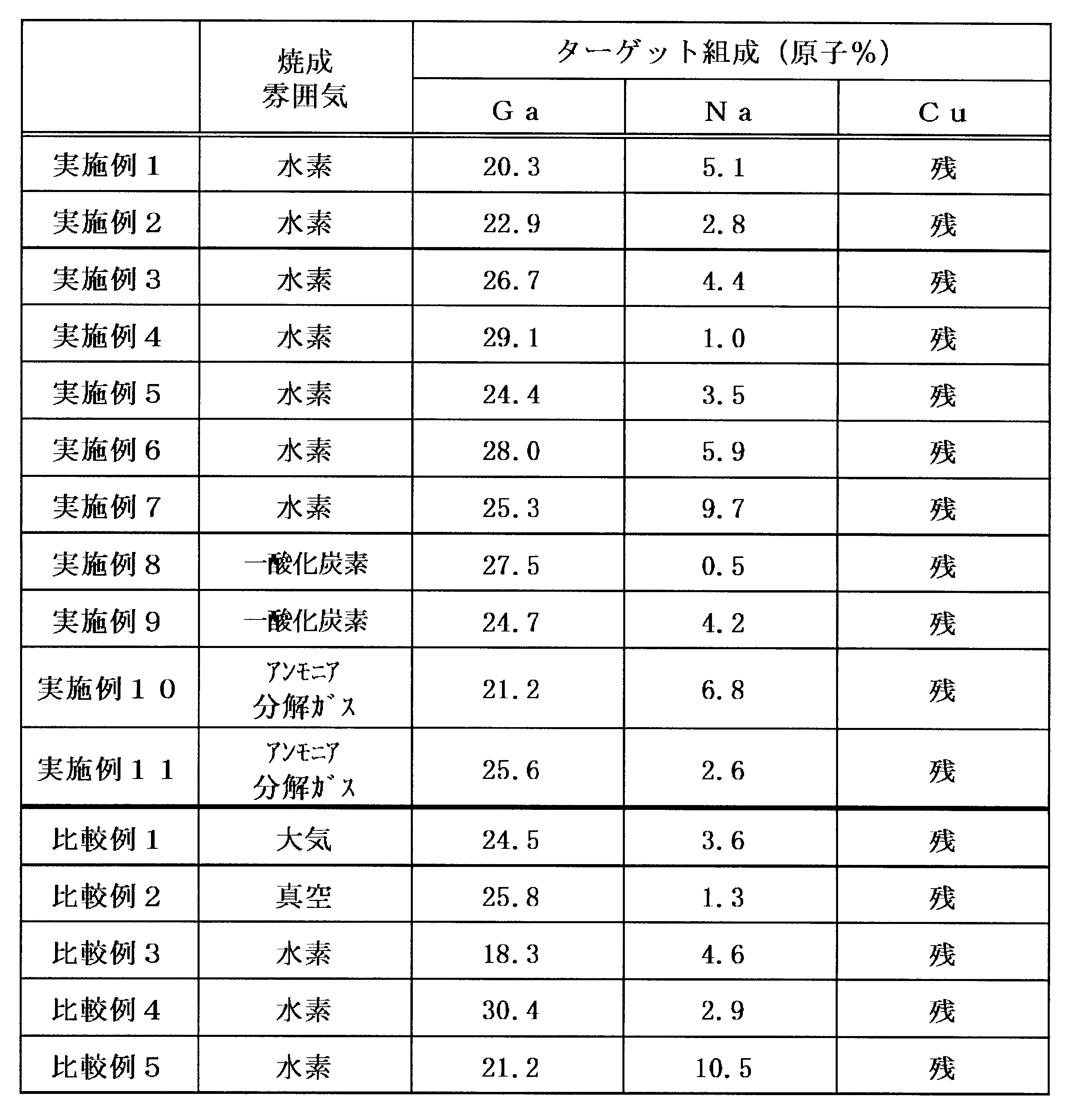
このように作製した本発明の実施例及び比較例のスパッタリングターゲットについて、γ相およびNa化合物相の平均粒径と、Na化合物相の最大粒径と、X線回折による分析と、酸素含有量と、異常放電回数とについて調べた結果が表3に示されている。
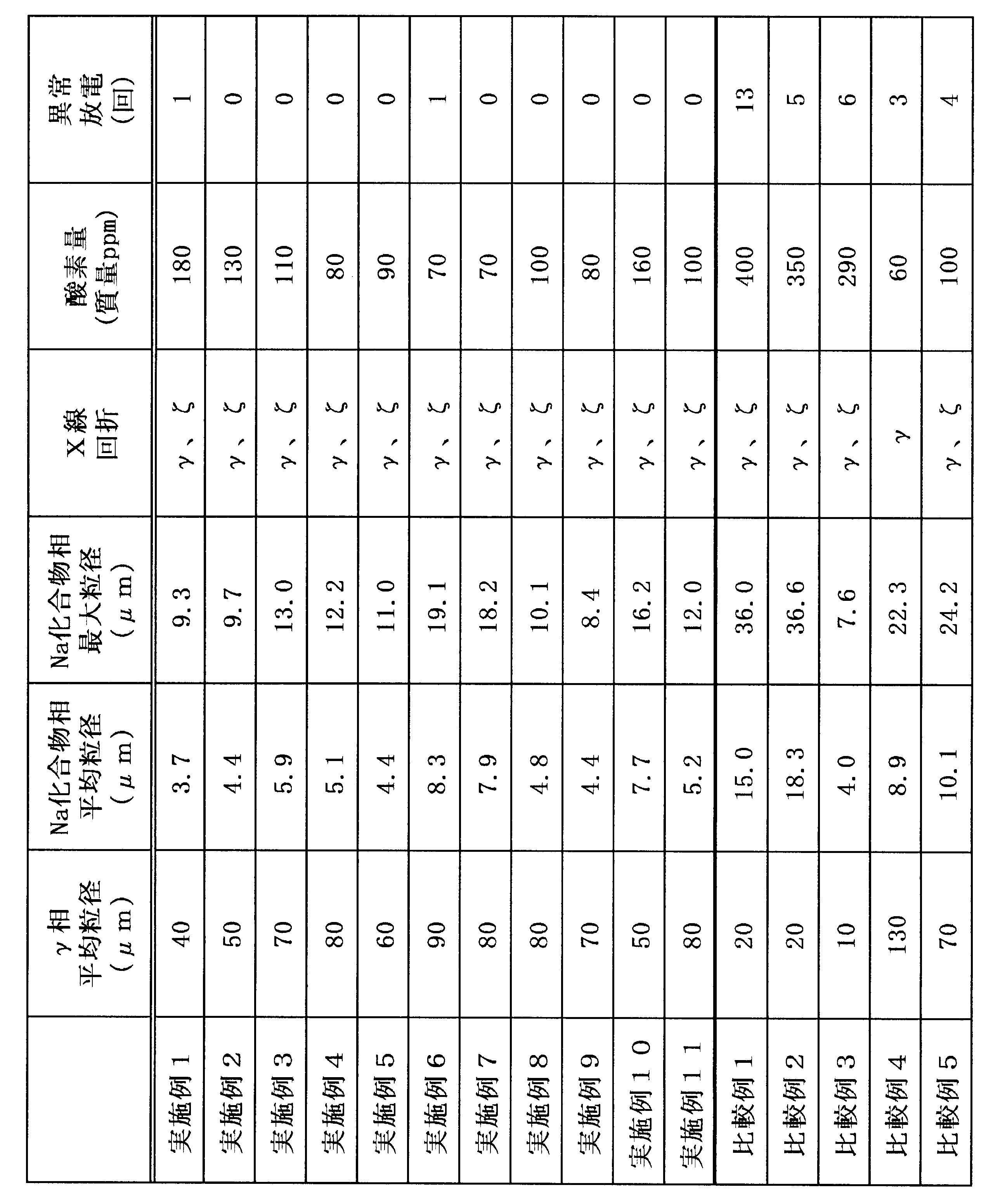
また、X線回折による分析では、γ相に帰属する回折ピークとζ相に帰属する回折ピークとの両方が観察され、ζ相に帰属する回折ピークの主ピーク強度が、γ相に帰属する回折ピークの主ピーク強度の5%以上である場合を、表3において「γ、ζ」と表記し、ζ相に帰属する回折ピークの主ピーク強度が、γ相に帰属する回折ピークの主ピーク強度の5%未満である場合を、表3において「γ」と表記した。
この分析に使用した装置及び測定条件を以下に示す。
装置:理学電気社製(RINT-Ultima/PC)
管球:Cu
管電圧:40kV
管電流:40mA
走査範囲(2θ):20°~120°
測定ステップ幅:2θで0.02°
スキャンスピード:毎分2°
装置:理学電気社製(RINT-Ultima/PC)
管球:Cu
管電圧:40kV
管電流:40mA
走査範囲(2θ):20°~120°
測定ステップ幅:2θで0.02°
スキャンスピード:毎分2°
また、異常放電については、下記の成膜条件で12時間スパッタを行い、異常放電の回数を測定した。
・電源:パルスDC500W
・全圧:0.4Pa
・スパッタガス:Ar=47.5sccm、O2=2.5sccm
・ターゲット-基板(TS)距離:70mm
・異常放電回数は、MKSインスツルメンツ社製DC電源(型番:RPDG-50A)のアークカウント機能により計測した。
・電源:パルスDC500W
・全圧:0.4Pa
・スパッタガス:Ar=47.5sccm、O2=2.5sccm
・ターゲット-基板(TS)距離:70mm
・異常放電回数は、MKSインスツルメンツ社製DC電源(型番:RPDG-50A)のアークカウント機能により計測した。
これらの結果からわかるように、本発明の実施例のスパッタリングターゲットは、いずれもγ相の平均粒径が40~90μmと小さく、X線回折においてはγ相とζ相との2相が観察されている。また、これら実施例のスパッタリングターゲットでは、酸素含有量が70~180質量ppmと非常に少なく、かつ、Na化合物相の平均粒径及び最大粒径が小さいため、異常放電回数も、1回以下と大幅に低減されている。
これらに対して、大気中で常圧焼結した比較例1のスパッタリングターゲットでは、酸素含有量が400質量ppmと高いと共に、異常放電回数が13回と大幅に増加してしまっている。また、Gaが本発明の組成範囲から外れて少ない比較例3のスパッタリングターゲットでは、酸素含有量が290質量ppmと増えていると共に異常放電回数も6回に増えてしまっている。さらに、Gaが本発明の組成範囲から外れて多い比較例4のスパッタリングターゲットでは、ほぼγ相の単相になってしまい、異常放電回数も3回に増えてしまっている。
また、ホットプレス法により焼成された比較例2のスパッタリングターゲットでは、酸素含有量が350質量ppmに増大してしまい、異常放電回数も5回に増えてしまっている。
次に、Gaの含有量を22.9原子%、29.1原子%、30.4原子%とした本発明の実施例及び比較例を、それぞれ50L/minで水素ガスを流しつつ、840℃の焼成温度で5時間保持する常圧焼結で作製し、X線回折(XRD)による回折ピークを測定した結果を、図2~図4に示す。
これらの結果からわかるように、Gaの含有量が22.9原子%、29.1原子%では、CuGaのγ相(Cu9Ga4相)に帰属する回折ピークとζ相(Cu3Ga相)に帰属する回折ピークとが両方観察され、ζ相に帰属する回折ピークの主ピーク強度が、γ相に帰属する回折ピークの主ピーク強度の5%以上であることから、γ相とζ相との2相が明確に組織中に形成されていることがわかる。しかしながら、Gaの含有量が30.4原子%になると、ζ相に帰属する回折ピークが5%未満になり、組織がほぼγ相の単相になってしまっていることがわかる。
次に、Gaを22.9原子%含有する実施例2のスパッタリングターゲットを、50L/minで水素ガスを流しつつ、840℃の焼成温度で5時間保持して常圧焼結を行い作製した。得られた組織のEPMAによって観察した組成像(COMPO像)と、Gaの元素マッピング像を、図5及び図6に示す。COMPO像においては、最も白い部分がGaの含有量が焼成体に対して相対的に高い領域を示している。Gaの元素マッピング像は、元画像がカラー像であるが、グレースケールによる白黒画像に変換して記載しており、明度が暗い部分でGa含有量が高い傾向にある。これらの画像からわかるように、本発明の実施例では、焼成体に対して相対的にGaが多く含有されている相(Ga-rich領域)が分散した結晶組織を有している。
なお、本発明を、スパッタリングターゲットとして利用するためには、面粗さ:1.5μm以下、電気抵抗:1×10⁻⁴Ω・cm以下、不純物金属量:0.1原子%以下、抗折強度:150MPa以上であることが好ましい。上記各実施例は、いずれもこれらの条件を満たしたものである。
また、本発明の技術範囲は上記実施形態および上記実施例に限定されるものではなく、本発明の趣旨を逸脱しない範囲において種々の変更を加えることが可能である。
例えば、上記実施形態及び上記実施例のスパッタリングターゲットは、平板状のものであるが、円筒状のスパッタリングターゲットとしても構わない。より具体的には、円盤板形状、短形板形状、多角形板形状、および楕円板形状等の板状、または円筒形状であってもよい。
また、本発明の技術範囲は上記実施形態および上記実施例に限定されるものではなく、本発明の趣旨を逸脱しない範囲において種々の変更を加えることが可能である。
例えば、上記実施形態及び上記実施例のスパッタリングターゲットは、平板状のものであるが、円筒状のスパッタリングターゲットとしても構わない。より具体的には、円盤板形状、短形板形状、多角形板形状、および楕円板形状等の板状、または円筒形状であってもよい。
本発明のAg-In合金スパッタリングターゲットを用いてスパッタリングすることにより、安定した成膜を行うことができる。
Claims (6)
- Cu-Ga合金のγ相及びζ相を有する素地中に、Na化合物相が分散した組織を有し、Ga:20~30原子%、Na:0.05~10原子%を含有し、残部がCu及び不可避不純物(Na化合物におけるNa以外の元素を含む)からなる成分組成を有する焼成体であって、
前記γ相の平均粒径が、30~100μmであり、
前記Na化合物相の平均粒径が、8.5μm以下であることを特徴とするCu-Ga合金スパッタリングターゲット。 - 前記Na化合物相の最大粒径が20μm以下であることを特徴とする請求項1に記載のCu-Ga合金スパッタリングターゲット。
- 前記ζ相に帰属するX線回折の主ピーク強度が、前記γ相に帰属するX線回折の主ピーク強度の5%以上であることを特徴とする請求項1又は2に記載のCu-Ga合金スパッタリングターゲット。
- 前記Na化合物相は、NaF、Na2S、Na2Se及びNa3AlF6の少なくとも1種以上からなることを特徴とする請求項1~3のいずれかに記載のCu-Ga合金スパッタリングターゲット。
- 前記焼成体の酸素含有量は、200質量ppm以下であることを特徴とする請求項1~4のいずれかに記載のCu-Ga合金スパッタリングターゲット。
- 請求項1~5のいずれかに記載のCu-Ga合金スパッタリングターゲットを製造する方法であって、
純Cu粉末、Cu-Ga合金粉末及びNa化合物との混合粉末からなる成形体を、還元性雰囲気中で加熱して常圧焼結する工程を有することを特徴とするCu-Ga合金スパッタリングターゲットの製造方法。
Priority Applications (3)
| Application Number | Priority Date | Filing Date | Title |
|---|---|---|---|
| EP14831218.4A EP3029171A4 (en) | 2013-08-01 | 2014-07-25 | Cu-ga alloy sputtering target, and method for producing same |
| US14/908,346 US10017850B2 (en) | 2013-08-01 | 2014-07-25 | Cu—Ga alloy sputtering target, and method for producing same |
| CN201480038680.4A CN105358733B (zh) | 2013-08-01 | 2014-07-25 | Cu‑Ga合金溅射靶及其制造方法 |
Applications Claiming Priority (2)
| Application Number | Priority Date | Filing Date | Title |
|---|---|---|---|
| JP2013-160134 | 2013-08-01 | ||
| JP2013160134A JP6120076B2 (ja) | 2013-08-01 | 2013-08-01 | Cu−Ga合金スパッタリングターゲット及びその製造方法 |
Publications (1)
| Publication Number | Publication Date |
|---|---|
| WO2015016153A1 true WO2015016153A1 (ja) | 2015-02-05 |
Family
ID=52431688
Family Applications (1)
| Application Number | Title | Priority Date | Filing Date |
|---|---|---|---|
| PCT/JP2014/069735 Ceased WO2015016153A1 (ja) | 2013-08-01 | 2014-07-25 | Cu-Ga合金スパッタリングターゲット及びその製造方法 |
Country Status (6)
| Country | Link |
|---|---|
| US (1) | US10017850B2 (ja) |
| EP (1) | EP3029171A4 (ja) |
| JP (1) | JP6120076B2 (ja) |
| CN (1) | CN105358733B (ja) |
| TW (1) | TWI617681B (ja) |
| WO (1) | WO2015016153A1 (ja) |
Families Citing this family (8)
| Publication number | Priority date | Publication date | Assignee | Title |
|---|---|---|---|---|
| JP6147788B2 (ja) * | 2015-03-26 | 2017-06-14 | Jx金属株式会社 | Cu−Ga合金スパッタリングターゲット |
| WO2017134999A1 (ja) * | 2016-02-03 | 2017-08-10 | 三菱マテリアル株式会社 | Cu-Ga合金スパッタリングターゲットの製造方法、及び、Cu-Ga合金スパッタリングターゲット |
| JP6888294B2 (ja) * | 2016-02-03 | 2021-06-16 | 三菱マテリアル株式会社 | Cu−Ga合金スパッタリングターゲットの製造方法、及び、Cu−Ga合金スパッタリングターゲット |
| JP6794850B2 (ja) * | 2016-02-08 | 2020-12-02 | 三菱マテリアル株式会社 | スパッタリングターゲット及びスパッタリングターゲットの製造方法 |
| JP2019044222A (ja) * | 2017-08-31 | 2019-03-22 | 三菱マテリアル株式会社 | In−Cu合金粉末、In−Cu合金粉末の製造方法、In−Cu合金スパッタリングターゲット及びIn−Cu合金スパッタリングターゲットの製造方法 |
| JP2019112671A (ja) * | 2017-12-22 | 2019-07-11 | 三菱マテリアル株式会社 | Cu−Ga合金スパッタリングターゲット、及び、Cu−Ga合金スパッタリングターゲットの製造方法 |
| JP6531816B1 (ja) | 2017-12-22 | 2019-06-19 | 三菱マテリアル株式会社 | Cu−Ga合金スパッタリングターゲット、及び、Cu−Ga合金スパッタリングターゲットの製造方法 |
| JP2019183277A (ja) * | 2018-04-04 | 2019-10-24 | 三菱マテリアル株式会社 | Cu−Ga合金スパッタリングターゲット |
Citations (5)
| Publication number | Priority date | Publication date | Assignee | Title |
|---|---|---|---|---|
| JPH10135495A (ja) | 1996-10-25 | 1998-05-22 | Showa Shell Sekiyu Kk | 薄膜太陽電池の製造方法及び製造装置 |
| JP2010265544A (ja) * | 2009-04-14 | 2010-11-25 | Kobelco Kaken:Kk | Cu−Ga合金スパッタリングターゲットおよびその製造方法 |
| WO2011010529A1 (ja) | 2009-07-23 | 2011-01-27 | Jx日鉱日石金属株式会社 | Cu-Ga合金焼結体スパッタリングターゲット、同ターゲットの製造方法、Cu-Ga合金焼結体ターゲットから作製された光吸収層及び同光吸収層を用いたCIGS系太陽電池 |
| US7935558B1 (en) | 2010-10-19 | 2011-05-03 | Miasole | Sodium salt containing CIG targets, methods of making and methods of use thereof |
| JP2011214140A (ja) * | 2010-03-18 | 2011-10-27 | Mitsubishi Materials Corp | スパッタリングターゲット及びその製造方法 |
Family Cites Families (3)
| Publication number | Priority date | Publication date | Assignee | Title |
|---|---|---|---|---|
| JP4793504B2 (ja) | 2009-11-06 | 2011-10-12 | 三菱マテリアル株式会社 | スパッタリングターゲット及びその製造方法 |
| JP2012017481A (ja) * | 2010-07-06 | 2012-01-26 | Mitsui Mining & Smelting Co Ltd | Cu−Ga合金およびCu−Ga合金スパッタリングターゲット |
| JP5725610B2 (ja) | 2011-04-29 | 2015-05-27 | 三菱マテリアル株式会社 | スパッタリングターゲット及びその製造方法 |
-
2013
- 2013-08-01 JP JP2013160134A patent/JP6120076B2/ja not_active Expired - Fee Related
-
2014
- 2014-07-25 CN CN201480038680.4A patent/CN105358733B/zh not_active Expired - Fee Related
- 2014-07-25 US US14/908,346 patent/US10017850B2/en active Active
- 2014-07-25 WO PCT/JP2014/069735 patent/WO2015016153A1/ja not_active Ceased
- 2014-07-25 EP EP14831218.4A patent/EP3029171A4/en not_active Withdrawn
- 2014-07-29 TW TW103125861A patent/TWI617681B/zh active
Patent Citations (5)
| Publication number | Priority date | Publication date | Assignee | Title |
|---|---|---|---|---|
| JPH10135495A (ja) | 1996-10-25 | 1998-05-22 | Showa Shell Sekiyu Kk | 薄膜太陽電池の製造方法及び製造装置 |
| JP2010265544A (ja) * | 2009-04-14 | 2010-11-25 | Kobelco Kaken:Kk | Cu−Ga合金スパッタリングターゲットおよびその製造方法 |
| WO2011010529A1 (ja) | 2009-07-23 | 2011-01-27 | Jx日鉱日石金属株式会社 | Cu-Ga合金焼結体スパッタリングターゲット、同ターゲットの製造方法、Cu-Ga合金焼結体ターゲットから作製された光吸収層及び同光吸収層を用いたCIGS系太陽電池 |
| JP2011214140A (ja) * | 2010-03-18 | 2011-10-27 | Mitsubishi Materials Corp | スパッタリングターゲット及びその製造方法 |
| US7935558B1 (en) | 2010-10-19 | 2011-05-03 | Miasole | Sodium salt containing CIG targets, methods of making and methods of use thereof |
Non-Patent Citations (2)
| Title |
|---|
| ISHIZUKA ET AL.: "Recent Developments in Chalcopyrite Solar Cell and Module Technologies", JOURNAL OF THE VACUUM SOCIETY OF JAPAN, vol. 53, 2010, pages 25 |
| See also references of EP3029171A4 |
Also Published As
| Publication number | Publication date |
|---|---|
| TWI617681B (zh) | 2018-03-11 |
| CN105358733B (zh) | 2018-01-26 |
| TW201510250A (zh) | 2015-03-16 |
| JP2015030870A (ja) | 2015-02-16 |
| EP3029171A4 (en) | 2017-03-29 |
| US20160208376A1 (en) | 2016-07-21 |
| EP3029171A1 (en) | 2016-06-08 |
| JP6120076B2 (ja) | 2017-04-26 |
| CN105358733A (zh) | 2016-02-24 |
| US10017850B2 (en) | 2018-07-10 |
Similar Documents
| Publication | Publication Date | Title |
|---|---|---|
| JP6120076B2 (ja) | Cu−Ga合金スパッタリングターゲット及びその製造方法 | |
| JP5725610B2 (ja) | スパッタリングターゲット及びその製造方法 | |
| TWI583811B (zh) | A Cu-Ga sputtering target, a method for manufacturing the target, a light absorbing layer, and a solar cell using the light absorbing layer | |
| JP5730788B2 (ja) | スパッタリングターゲット及びスパッタリングターゲットの製造方法 | |
| JP5907428B2 (ja) | スパッタリングターゲット及びその製造方法 | |
| JP5999357B2 (ja) | スパッタリングターゲット及びその製造方法 | |
| TWI666333B (zh) | Cu-Ga合金濺鍍靶及其製造方法 | |
| JP5743119B1 (ja) | Cu−Ga合金スパッタリングターゲット及びその製造方法 | |
| WO2014024975A1 (ja) | スパッタリングターゲット及びその製造方法 | |
| JP2012246574A (ja) | スパッタリングターゲット及びその製造方法 | |
| CN105473758B (zh) | 溅射靶及其制造方法 | |
| TWI586824B (zh) | Sputtering target and its manufacturing method | |
| JP2017014599A (ja) | スパッタリングターゲット及びその製造方法 | |
| JP2016082120A (ja) | 太陽電池用光吸収層およびその製造方法、並びに前記太陽電池用光吸収層を有する太陽電池 |
Legal Events
| Date | Code | Title | Description |
|---|---|---|---|
| WWE | Wipo information: entry into national phase |
Ref document number: 201480038680.4 Country of ref document: CN |
|
| 121 | Ep: the epo has been informed by wipo that ep was designated in this application |
Ref document number: 14831218 Country of ref document: EP Kind code of ref document: A1 |
|
| WWE | Wipo information: entry into national phase |
Ref document number: 2014831218 Country of ref document: EP |
|
| WWE | Wipo information: entry into national phase |
Ref document number: 14908346 Country of ref document: US |
|
| NENP | Non-entry into the national phase |
Ref country code: DE |