WO2015019707A1 - 炭化珪素半導体基板およびその製造方法、ならびに炭化珪素半導体装置の製造方法 - Google Patents
炭化珪素半導体基板およびその製造方法、ならびに炭化珪素半導体装置の製造方法 Download PDFInfo
- Publication number
- WO2015019707A1 WO2015019707A1 PCT/JP2014/065712 JP2014065712W WO2015019707A1 WO 2015019707 A1 WO2015019707 A1 WO 2015019707A1 JP 2014065712 W JP2014065712 W JP 2014065712W WO 2015019707 A1 WO2015019707 A1 WO 2015019707A1
- Authority
- WO
- WIPO (PCT)
- Prior art keywords
- silicon carbide
- carbide semiconductor
- semiconductor substrate
- substrate
- main surface
- Prior art date
- Legal status (The legal status is an assumption and is not a legal conclusion. Google has not performed a legal analysis and makes no representation as to the accuracy of the status listed.)
- Ceased
Links
Images






Classifications
-
- H—ELECTRICITY
- H10—SEMICONDUCTOR DEVICES; ELECTRIC SOLID-STATE DEVICES NOT OTHERWISE PROVIDED FOR
- H10P—GENERIC PROCESSES OR APPARATUS FOR THE MANUFACTURE OR TREATMENT OF DEVICES COVERED BY CLASS H10
- H10P14/00—Formation of materials, e.g. in the shape of layers or pillars
- H10P14/20—Formation of materials, e.g. in the shape of layers or pillars of semiconductor materials
-
- H—ELECTRICITY
- H10—SEMICONDUCTOR DEVICES; ELECTRIC SOLID-STATE DEVICES NOT OTHERWISE PROVIDED FOR
- H10P—GENERIC PROCESSES OR APPARATUS FOR THE MANUFACTURE OR TREATMENT OF DEVICES COVERED BY CLASS H10
- H10P14/00—Formation of materials, e.g. in the shape of layers or pillars
- H10P14/20—Formation of materials, e.g. in the shape of layers or pillars of semiconductor materials
- H10P14/34—Deposited materials, e.g. layers
- H10P14/3402—Deposited materials, e.g. layers characterised by the chemical composition
- H10P14/3404—Deposited materials, e.g. layers characterised by the chemical composition being Group IVA materials
- H10P14/3408—Silicon carbide
-
- H—ELECTRICITY
- H10—SEMICONDUCTOR DEVICES; ELECTRIC SOLID-STATE DEVICES NOT OTHERWISE PROVIDED FOR
- H10D—INORGANIC ELECTRIC SEMICONDUCTOR DEVICES
- H10D12/00—Bipolar devices controlled by the field effect, e.g. insulated-gate bipolar transistors [IGBT]
- H10D12/01—Manufacture or treatment
- H10D12/031—Manufacture or treatment of IGBTs
-
- H—ELECTRICITY
- H10—SEMICONDUCTOR DEVICES; ELECTRIC SOLID-STATE DEVICES NOT OTHERWISE PROVIDED FOR
- H10D—INORGANIC ELECTRIC SEMICONDUCTOR DEVICES
- H10D30/00—Field-effect transistors [FET]
- H10D30/60—Insulated-gate field-effect transistors [IGFET]
-
- H—ELECTRICITY
- H10—SEMICONDUCTOR DEVICES; ELECTRIC SOLID-STATE DEVICES NOT OTHERWISE PROVIDED FOR
- H10D—INORGANIC ELECTRIC SEMICONDUCTOR DEVICES
- H10D30/00—Field-effect transistors [FET]
- H10D30/60—Insulated-gate field-effect transistors [IGFET]
- H10D30/64—Double-diffused metal-oxide semiconductor [DMOS] FETs
- H10D30/66—Vertical DMOS [VDMOS] FETs
- H10D30/665—Vertical DMOS [VDMOS] FETs having edge termination structures
-
- H—ELECTRICITY
- H10—SEMICONDUCTOR DEVICES; ELECTRIC SOLID-STATE DEVICES NOT OTHERWISE PROVIDED FOR
- H10D—INORGANIC ELECTRIC SEMICONDUCTOR DEVICES
- H10D62/00—Semiconductor bodies, or regions thereof, of devices having potential barriers
- H10D62/10—Shapes, relative sizes or dispositions of the regions of the semiconductor bodies; Shapes of the semiconductor bodies
-
- H—ELECTRICITY
- H10—SEMICONDUCTOR DEVICES; ELECTRIC SOLID-STATE DEVICES NOT OTHERWISE PROVIDED FOR
- H10D—INORGANIC ELECTRIC SEMICONDUCTOR DEVICES
- H10D62/00—Semiconductor bodies, or regions thereof, of devices having potential barriers
- H10D62/10—Shapes, relative sizes or dispositions of the regions of the semiconductor bodies; Shapes of the semiconductor bodies
- H10D62/102—Constructional design considerations for preventing surface leakage or controlling electric field concentration
- H10D62/103—Constructional design considerations for preventing surface leakage or controlling electric field concentration for increasing or controlling the breakdown voltage of reverse-biased devices
- H10D62/105—Constructional design considerations for preventing surface leakage or controlling electric field concentration for increasing or controlling the breakdown voltage of reverse-biased devices by having particular doping profiles, shapes or arrangements of PN junctions; by having supplementary regions, e.g. junction termination extension [JTE]
- H10D62/106—Constructional design considerations for preventing surface leakage or controlling electric field concentration for increasing or controlling the breakdown voltage of reverse-biased devices by having particular doping profiles, shapes or arrangements of PN junctions; by having supplementary regions, e.g. junction termination extension [JTE] having supplementary regions doped oppositely to or in rectifying contact with regions of the semiconductor bodies, e.g. guard rings with PN or Schottky junctions
-
- H—ELECTRICITY
- H10—SEMICONDUCTOR DEVICES; ELECTRIC SOLID-STATE DEVICES NOT OTHERWISE PROVIDED FOR
- H10D—INORGANIC ELECTRIC SEMICONDUCTOR DEVICES
- H10D62/00—Semiconductor bodies, or regions thereof, of devices having potential barriers
- H10D62/80—Semiconductor bodies, or regions thereof, of devices having potential barriers characterised by the materials
- H10D62/81—Semiconductor bodies, or regions thereof, of devices having potential barriers characterised by the materials of structures exhibiting quantum-confinement effects, e.g. single quantum wells; of structures having periodic or quasi-periodic potential variation
-
- H—ELECTRICITY
- H10—SEMICONDUCTOR DEVICES; ELECTRIC SOLID-STATE DEVICES NOT OTHERWISE PROVIDED FOR
- H10D—INORGANIC ELECTRIC SEMICONDUCTOR DEVICES
- H10D62/00—Semiconductor bodies, or regions thereof, of devices having potential barriers
- H10D62/80—Semiconductor bodies, or regions thereof, of devices having potential barriers characterised by the materials
- H10D62/83—Semiconductor bodies, or regions thereof, of devices having potential barriers characterised by the materials being Group IV materials, e.g. B-doped Si or undoped Ge
- H10D62/832—Semiconductor bodies, or regions thereof, of devices having potential barriers characterised by the materials being Group IV materials, e.g. B-doped Si or undoped Ge being Group IV materials comprising two or more elements, e.g. SiGe
- H10D62/8325—Silicon carbide
-
- H—ELECTRICITY
- H10—SEMICONDUCTOR DEVICES; ELECTRIC SOLID-STATE DEVICES NOT OTHERWISE PROVIDED FOR
- H10P—GENERIC PROCESSES OR APPARATUS FOR THE MANUFACTURE OR TREATMENT OF DEVICES COVERED BY CLASS H10
- H10P14/00—Formation of materials, e.g. in the shape of layers or pillars
- H10P14/20—Formation of materials, e.g. in the shape of layers or pillars of semiconductor materials
- H10P14/24—Formation of materials, e.g. in the shape of layers or pillars of semiconductor materials using chemical vapour deposition [CVD]
-
- H—ELECTRICITY
- H10—SEMICONDUCTOR DEVICES; ELECTRIC SOLID-STATE DEVICES NOT OTHERWISE PROVIDED FOR
- H10P—GENERIC PROCESSES OR APPARATUS FOR THE MANUFACTURE OR TREATMENT OF DEVICES COVERED BY CLASS H10
- H10P14/00—Formation of materials, e.g. in the shape of layers or pillars
- H10P14/20—Formation of materials, e.g. in the shape of layers or pillars of semiconductor materials
- H10P14/29—Formation of materials, e.g. in the shape of layers or pillars of semiconductor materials characterised by the substrates
- H10P14/2901—Materials
- H10P14/2902—Materials being Group IVA materials
- H10P14/2904—Silicon carbide
-
- H—ELECTRICITY
- H10—SEMICONDUCTOR DEVICES; ELECTRIC SOLID-STATE DEVICES NOT OTHERWISE PROVIDED FOR
- H10P—GENERIC PROCESSES OR APPARATUS FOR THE MANUFACTURE OR TREATMENT OF DEVICES COVERED BY CLASS H10
- H10P14/00—Formation of materials, e.g. in the shape of layers or pillars
- H10P14/20—Formation of materials, e.g. in the shape of layers or pillars of semiconductor materials
- H10P14/29—Formation of materials, e.g. in the shape of layers or pillars of semiconductor materials characterised by the substrates
- H10P14/2924—Structures
-
- H—ELECTRICITY
- H10—SEMICONDUCTOR DEVICES; ELECTRIC SOLID-STATE DEVICES NOT OTHERWISE PROVIDED FOR
- H10P—GENERIC PROCESSES OR APPARATUS FOR THE MANUFACTURE OR TREATMENT OF DEVICES COVERED BY CLASS H10
- H10P14/00—Formation of materials, e.g. in the shape of layers or pillars
- H10P14/60—Formation of materials, e.g. in the shape of layers or pillars of insulating materials
- H10P14/63—Formation of materials, e.g. in the shape of layers or pillars of insulating materials characterised by the formation processes
- H10P14/6302—Non-deposition formation processes
- H10P14/6304—Formation by oxidation, e.g. oxidation of the substrate
- H10P14/6306—Formation by oxidation, e.g. oxidation of the substrate of the semiconductor materials
- H10P14/6308—Formation by oxidation, e.g. oxidation of the substrate of the semiconductor materials of Group IV semiconductors
-
- H—ELECTRICITY
- H10—SEMICONDUCTOR DEVICES; ELECTRIC SOLID-STATE DEVICES NOT OTHERWISE PROVIDED FOR
- H10P—GENERIC PROCESSES OR APPARATUS FOR THE MANUFACTURE OR TREATMENT OF DEVICES COVERED BY CLASS H10
- H10P30/00—Ion implantation into wafers, substrates or parts of devices
- H10P30/20—Ion implantation into wafers, substrates or parts of devices into semiconductor materials, e.g. for doping
- H10P30/202—Ion implantation into wafers, substrates or parts of devices into semiconductor materials, e.g. for doping characterised by the semiconductor materials
- H10P30/204—Ion implantation into wafers, substrates or parts of devices into semiconductor materials, e.g. for doping characterised by the semiconductor materials into Group IV semiconductors
-
- H—ELECTRICITY
- H10—SEMICONDUCTOR DEVICES; ELECTRIC SOLID-STATE DEVICES NOT OTHERWISE PROVIDED FOR
- H10P—GENERIC PROCESSES OR APPARATUS FOR THE MANUFACTURE OR TREATMENT OF DEVICES COVERED BY CLASS H10
- H10P30/00—Ion implantation into wafers, substrates or parts of devices
- H10P30/20—Ion implantation into wafers, substrates or parts of devices into semiconductor materials, e.g. for doping
- H10P30/202—Ion implantation into wafers, substrates or parts of devices into semiconductor materials, e.g. for doping characterised by the semiconductor materials
- H10P30/204—Ion implantation into wafers, substrates or parts of devices into semiconductor materials, e.g. for doping characterised by the semiconductor materials into Group IV semiconductors
- H10P30/2042—Ion implantation into wafers, substrates or parts of devices into semiconductor materials, e.g. for doping characterised by the semiconductor materials into Group IV semiconductors into crystalline silicon carbide
-
- H—ELECTRICITY
- H10—SEMICONDUCTOR DEVICES; ELECTRIC SOLID-STATE DEVICES NOT OTHERWISE PROVIDED FOR
- H10P—GENERIC PROCESSES OR APPARATUS FOR THE MANUFACTURE OR TREATMENT OF DEVICES COVERED BY CLASS H10
- H10P30/00—Ion implantation into wafers, substrates or parts of devices
- H10P30/20—Ion implantation into wafers, substrates or parts of devices into semiconductor materials, e.g. for doping
- H10P30/208—Ion implantation into wafers, substrates or parts of devices into semiconductor materials, e.g. for doping of electrically inactive species
-
- H—ELECTRICITY
- H10—SEMICONDUCTOR DEVICES; ELECTRIC SOLID-STATE DEVICES NOT OTHERWISE PROVIDED FOR
- H10P—GENERIC PROCESSES OR APPARATUS FOR THE MANUFACTURE OR TREATMENT OF DEVICES COVERED BY CLASS H10
- H10P30/00—Ion implantation into wafers, substrates or parts of devices
- H10P30/20—Ion implantation into wafers, substrates or parts of devices into semiconductor materials, e.g. for doping
- H10P30/21—Ion implantation into wafers, substrates or parts of devices into semiconductor materials, e.g. for doping of electrically active species
-
- H—ELECTRICITY
- H10—SEMICONDUCTOR DEVICES; ELECTRIC SOLID-STATE DEVICES NOT OTHERWISE PROVIDED FOR
- H10P—GENERIC PROCESSES OR APPARATUS FOR THE MANUFACTURE OR TREATMENT OF DEVICES COVERED BY CLASS H10
- H10P30/00—Ion implantation into wafers, substrates or parts of devices
- H10P30/20—Ion implantation into wafers, substrates or parts of devices into semiconductor materials, e.g. for doping
- H10P30/222—Ion implantation into wafers, substrates or parts of devices into semiconductor materials, e.g. for doping characterised by the angle between the ion beam and the crystal planes or the main crystal surface
-
- H—ELECTRICITY
- H10—SEMICONDUCTOR DEVICES; ELECTRIC SOLID-STATE DEVICES NOT OTHERWISE PROVIDED FOR
- H10P—GENERIC PROCESSES OR APPARATUS FOR THE MANUFACTURE OR TREATMENT OF DEVICES COVERED BY CLASS H10
- H10P30/00—Ion implantation into wafers, substrates or parts of devices
- H10P30/20—Ion implantation into wafers, substrates or parts of devices into semiconductor materials, e.g. for doping
- H10P30/28—Ion implantation into wafers, substrates or parts of devices into semiconductor materials, e.g. for doping characterised by an annealing step, e.g. for activation of dopants
-
- H—ELECTRICITY
- H10—SEMICONDUCTOR DEVICES; ELECTRIC SOLID-STATE DEVICES NOT OTHERWISE PROVIDED FOR
- H10P—GENERIC PROCESSES OR APPARATUS FOR THE MANUFACTURE OR TREATMENT OF DEVICES COVERED BY CLASS H10
- H10P50/00—Etching of wafers, substrates or parts of devices
-
- H—ELECTRICITY
- H10—SEMICONDUCTOR DEVICES; ELECTRIC SOLID-STATE DEVICES NOT OTHERWISE PROVIDED FOR
- H10P—GENERIC PROCESSES OR APPARATUS FOR THE MANUFACTURE OR TREATMENT OF DEVICES COVERED BY CLASS H10
- H10P50/00—Etching of wafers, substrates or parts of devices
- H10P50/20—Dry etching; Plasma etching; Reactive-ion etching
- H10P50/24—Dry etching; Plasma etching; Reactive-ion etching of semiconductor materials
- H10P50/242—Dry etching; Plasma etching; Reactive-ion etching of semiconductor materials of Group IV materials
-
- H—ELECTRICITY
- H10—SEMICONDUCTOR DEVICES; ELECTRIC SOLID-STATE DEVICES NOT OTHERWISE PROVIDED FOR
- H10P—GENERIC PROCESSES OR APPARATUS FOR THE MANUFACTURE OR TREATMENT OF DEVICES COVERED BY CLASS H10
- H10P50/00—Etching of wafers, substrates or parts of devices
- H10P50/20—Dry etching; Plasma etching; Reactive-ion etching
- H10P50/28—Dry etching; Plasma etching; Reactive-ion etching of insulating materials
- H10P50/282—Dry etching; Plasma etching; Reactive-ion etching of insulating materials of inorganic materials
- H10P50/283—Dry etching; Plasma etching; Reactive-ion etching of insulating materials of inorganic materials by chemical means
-
- H—ELECTRICITY
- H10—SEMICONDUCTOR DEVICES; ELECTRIC SOLID-STATE DEVICES NOT OTHERWISE PROVIDED FOR
- H10P—GENERIC PROCESSES OR APPARATUS FOR THE MANUFACTURE OR TREATMENT OF DEVICES COVERED BY CLASS H10
- H10P52/00—Grinding, lapping or polishing of wafers, substrates or parts of devices
- H10P52/40—Chemomechanical polishing [CMP]
- H10P52/402—Chemomechanical polishing [CMP] of semiconductor materials
-
- H—ELECTRICITY
- H10—SEMICONDUCTOR DEVICES; ELECTRIC SOLID-STATE DEVICES NOT OTHERWISE PROVIDED FOR
- H10P—GENERIC PROCESSES OR APPARATUS FOR THE MANUFACTURE OR TREATMENT OF DEVICES COVERED BY CLASS H10
- H10P90/00—Preparation of wafers not covered by a single main group of this subclass, e.g. wafer reinforcement
-
- H—ELECTRICITY
- H10—SEMICONDUCTOR DEVICES; ELECTRIC SOLID-STATE DEVICES NOT OTHERWISE PROVIDED FOR
- H10P—GENERIC PROCESSES OR APPARATUS FOR THE MANUFACTURE OR TREATMENT OF DEVICES COVERED BY CLASS H10
- H10P14/00—Formation of materials, e.g. in the shape of layers or pillars
- H10P14/60—Formation of materials, e.g. in the shape of layers or pillars of insulating materials
- H10P14/63—Formation of materials, e.g. in the shape of layers or pillars of insulating materials characterised by the formation processes
- H10P14/6302—Non-deposition formation processes
- H10P14/6322—Formation by thermal treatments
Definitions
- the present invention relates to a silicon carbide semiconductor substrate, a method for manufacturing the same, and a method for manufacturing a silicon carbide semiconductor device, and more particularly, a silicon carbide semiconductor substrate having high flatness even when heat-treated at a high temperature, a method for manufacturing the same, and a silicon carbide semiconductor device. It relates to the manufacturing method.
- SiC silicon carbide
- the silicon carbide semiconductor substrate is being increased in diameter.
- the outer diameter of the silicon carbide semiconductor substrate is, for example, about 6 inches, the flatness of the silicon carbide semiconductor substrate is impaired.
- JP 2012-214376 describes a SiC having a diameter of at least about 75 millimeters (3 inches), a strain of less than about 5 ⁇ m, a warp of less than about 5 mm, and a TTV of less than about 2.0 ⁇ m.
- a wafer is described. Specifically, by slicing the SiC boule into a wafer and starting the lapping process using a downward force that is less than the downward force required to fold the wafer on a double-sided wrapper. It is described that wafers with low distortion, warpage and TTV can be produced.
- the silicon carbide semiconductor substrate whose flatness deteriorates due to heat treatment at a high temperature has been confirmed.
- doping in a method for manufacturing a silicon carbide semiconductor device is performed by ion implantation at a high temperature, but a silicon carbide semiconductor substrate having poor flatness is difficult to be adsorbed on the electrostatic chuck stage of the implantation device. It has been confirmed that problems such as breakage of the substrate may occur depending on the type.
- Such deterioration of flatness at high temperatures is a particularly serious problem in a silicon carbide semiconductor substrate having a large diameter of 100 mm or more. That is, even if a silicon carbide semiconductor substrate having a large diameter (especially 100 mm or more) is used in order to obtain a silicon carbide semiconductor device efficiently, it is difficult to manufacture the silicon carbide semiconductor device with a high yield due to the deterioration of the flatness as described above. Met.
- a main object of the present invention is to provide a silicon carbide semiconductor substrate having high flatness even at high temperatures, a method for manufacturing the same, and a method for manufacturing a silicon carbide semiconductor device.
- Another object of the present invention is to provide a method for manufacturing a silicon carbide semiconductor device capable of manufacturing a silicon carbide semiconductor device with a high yield by using a large-diameter silicon carbide semiconductor substrate.
- Silicon carbide semiconductor substrate 10 has a main surface having an outer diameter of 100 mm or more, and includes a base substrate 1 made of single-crystal silicon carbide and an epitaxial layer 2 formed on main surface 1A. .
- Silicon carbide semiconductor substrate 10 has a warpage amount of ⁇ 100 ⁇ m to 100 ⁇ m when the substrate temperature is room temperature, and a warp amount of ⁇ 1.5 mm to 1.5 mm when the substrate temperature is 400 ° C.
- a method of manufacturing a silicon carbide semiconductor substrate according to the present invention includes a step of preparing a base substrate having a main surface having an outer diameter of 100 mm or more and made of single crystal silicon carbide, and forming an epitaxial layer on the main surface A step of removing at least a part of the back surface of the base substrate opposite to the main surface to prepare a silicon carbide semiconductor substrate; and a step of implanting impurity ions into the silicon carbide semiconductor substrate; Is provided.
- a silicon carbide semiconductor substrate having high flatness even at high temperatures can be obtained.
- FIG. 8 is a reference diagram for illustrating the function and effect of the method for manufacturing the silicon carbide semiconductor device according to the embodiment.
- FIG. 8 is a reference diagram for illustrating the function and effect of the method for manufacturing the silicon carbide semiconductor device according to the embodiment.
- silicon carbide semiconductor substrate 10 has a main surface 2A having an outer diameter of 100 mm or more, a base substrate 1 made of single-crystal silicon carbide, and a main surface 2A, the amount of warpage when the substrate temperature is room temperature is ⁇ 100 ⁇ m or more and 100 ⁇ m or less, and the amount of warpage when the substrate temperature is 400 ° C. is ⁇ 1.5 mm or more and 1 .5 mm or less.
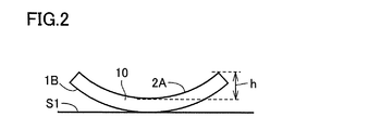
- “warping amount” of silicon carbide semiconductor substrate 10 means main surface 2 ⁇ / b> A of silicon carbide semiconductor substrate 10 when silicon carbide semiconductor substrate 10 is placed on plane S ⁇ b> 1. Is a difference in height between the highest position and the lowest position with respect to the plane S1.
- the amount of warpage is positive or negative when main surface 2A of silicon carbide semiconductor substrate 10 is convex downward (the center position of silicon carbide semiconductor substrate 10 is relative to plane S1 relative to the outer peripheral position).
- the case where it is convex upward is positive.
- “Substrate temperature” is a temperature measured by a radiation thermometer from the main surface 2A side of silicon carbide semiconductor substrate 10, and is measured in a semiconductor manufacturing apparatus such as an ion implantation apparatus, for example.
- Silicon carbide semiconductor substrate 10 according to the present embodiment is a large-diameter substrate having an outer diameter of 100 mm or more, preferably has an outer diameter of 125 mm or more, and more preferably has an outer diameter of 150 mm or more.
- silicon carbide semiconductor substrate 10 is a large-diameter substrate having an outer diameter of 100 mm or more, and a warpage amount when the substrate temperature is 400 ° C. is ⁇ 1.5 mm or more and 1.5 mm or less.
- the flatness is high even at high temperatures.
- doping in the method for manufacturing a silicon carbide semiconductor device is performed by ion implantation into silicon carbide semiconductor substrate 10 at a high temperature, and silicon carbide semiconductor substrate 10 is used as an electrostatic chuck stage of the ion implantation device.
- silicon carbide semiconductor substrate 10 is used as an electrostatic chuck stage of the ion implantation device.
- silicon carbide semiconductor substrate 10 is a large-diameter substrate having an outer diameter of 100 mm or more, and has high flatness even at high temperatures. Therefore, silicon carbide semiconductor substrate 10 is used to form a silicon carbide semiconductor device. When the manufacturing process is advanced, a silicon carbide semiconductor device having a small variation in characteristics can be manufactured on silicon carbide semiconductor substrate 10.
- region) with respect to 2A fluctuate locally within main surface 2A can be suppressed.
- variations in the processing on the main surface 2A can be reduced.
- silicon carbide semiconductor substrate 10 is required to have, for example, an LTV (Local Thickness Variation) of 1 ⁇ m or less in order to perform high-precision exposure.
- LTV Local Thickness Variation
- the silicon carbide semiconductor substrate 10 according to the present embodiment has a small amount of warpage, the apparent LTV does not increase and high-precision exposure can be performed.
- the silicon carbide semiconductor device can be manufactured with high yield by advancing the manufacturing process of the silicon carbide semiconductor device using silicon carbide semiconductor substrate 10 having a large diameter and high flatness.
- base substrate 1 in the direction perpendicular to main surfaces 1A and 2A may have a thickness of 200 ⁇ m or more and 700 ⁇ m or less. Even in this case, silicon carbide semiconductor substrate 10 according to the present embodiment can have a warpage amount of ⁇ 1.5 mm or more and 1.5 mm or less when the substrate temperature is 400 ° C.
- the thickness of epitaxial layer 2 formed on main surface 1A of base substrate 1 is about several ⁇ m or more and 100 ⁇ m or less. Therefore, when base substrate 1 is thin, the amount of warpage of silicon carbide semiconductor substrate 10 increases. On the other hand, when the thickness of the base substrate 1 is thick, the manufacturing cost increases.
- silicon carbide semiconductor substrate 10 according to the present embodiment can have high flatness even at a high temperature even if base substrate 1 does not have a thickness that exceeds 700 ⁇ m. That is, according to the method for manufacturing a silicon carbide substrate in accordance with the present embodiment, silicon carbide semiconductor substrate 10 having high flatness even at high temperatures can be obtained at low cost.
- the surface roughness of back surface 1B located on the opposite side of main surface 2A is preferably 10 nm or less.
- the surface roughness of the back surface 1B of the base substrate 1 is high, for example, silicon (Si) out of silicon carbide constituting the back surface 1B excessively escapes in a high temperature environment, and a carbonized layer (damage layer 3) is formed. It is thought that it is done.
- the inventors have described that a silicon carbide semiconductor substrate in which the surface roughness of the back surface 1B of the base substrate 1 after forming the epitaxial layer 2 on the main surface 1A of the base substrate 1 is 10 nm or less is the substrate temperature as described above.
- the amount of warping when the temperature was 400 ° C. was ⁇ 1.5 mm or more and 1.5 mm or less. That is, one of the causes of the increase in the amount of warp when the substrate temperature of silicon carbide semiconductor substrate 10 is high is the residual strain of damaged layer 3 formed on back surface 1B of base substrate 1 in silicon carbide semiconductor substrate 10. It is presumed that this is due to the stress caused by.
- a method for manufacturing a silicon carbide semiconductor substrate includes a step (S10) of preparing base substrate 1 having a main surface 2A having an outer diameter of 100 mm or more and made of single-crystal silicon carbide; A step (S30) of forming the epitaxial layer 2 on the main surface 2A and a step (S30) of removing at least a part of the back surface 1B located on the opposite side of the main surface 2A in the base substrate 1 are provided.
- the base substrate Part of the back surface 1B of 1 is removed. Thereby, even if the damage layer 3 is formed on the back surface 1B of the base substrate 1 in the step (S20) of forming the epitaxial layer 2, the damage layer 3 is removed in the step (S30) of removing a part of the back surface 1B of the base substrate 1. Removed.
- Silicon carbide semiconductor substrate 10 thus obtained has an outer diameter of 100 mm or more, a warpage amount when the substrate temperature is room temperature, of ⁇ 100 ⁇ m or more and 100 ⁇ m or less, and a substrate temperature of 400 ° C.
- the amount of warpage is not less than ⁇ 1.5 mm and not more than 1.5 mm. That is, according to the method for manufacturing a silicon carbide semiconductor substrate in accordance with the present embodiment, silicon carbide semiconductor substrate 10 having high flatness can be obtained even in an environment of high temperature even if the outer diameter is 100 mm or more.
- the removing step (S30) may be performed by chemically polishing the back surface 1B (Chemical Mechanical Polishing: CMP). Even if it does in this way, even if the damage layer 3 arises in the back surface 1B of the base substrate 1 in the process of forming the epitaxial layer 2 (S20), the damage layer 3 is reliably formed by chemically polishing the back surface 1B of the base substrate 1. Can be removed.
- CMP Chemical Mechanical Polishing
- the removing step (S30) may be performed by reactive ion etching of the back surface 1B. Even if it does in this way, even if the damage layer 3 arises in the back surface 1B of the base substrate 1 in the process (S20) of forming the epitaxial layer 2, the damage layer 3 is formed by reactive ion etching of the back surface 1B of the base substrate 1. It can be removed reliably.
- the removing step (S30) may be performed by thermally etching back surface 1B in a halogen gas atmosphere. Even if it does in this way, even if the damage layer 3 arises in the back surface 1B of the base substrate 1 in the process (S20) of forming the epitaxial layer 2, the damage layer 3 is reliably formed by thermally etching the back surface 1B of the base substrate 1. Can be removed.
- the thermal oxide film is etched using hydrofluoric acid. It may be done by. Even if it does in this way, even if the damage layer 3 arises in the back surface 1B of the base substrate 1 in the process (S20) of forming the epitaxial layer 2, the thermal oxide film formed on the back surface 1B of the base substrate 1 is made of hydrofluoric acid. The damage layer 3 can be reliably removed by using and etching.
- a method for manufacturing a silicon carbide semiconductor device includes a step (S10) of preparing base substrate 1 having a main surface 2A having an outer diameter of 100 mm or more and made of single-crystal silicon carbide; A step of forming epitaxial layer 2 on main surface 2A (S20) and a step of preparing silicon carbide semiconductor substrate 10 by removing at least part of back surface 1B located on the opposite side of main surface 2A in base substrate 1 (S30) and a step of implanting impurity ions into silicon carbide semiconductor substrate 10 (S40).
- the method for manufacturing the silicon carbide semiconductor device according to the present embodiment uses silicon carbide semiconductor substrate 10 obtained by the method for manufacturing the silicon carbide semiconductor substrate according to the present embodiment, and carbonizes on silicon carbide semiconductor substrate 10.
- a silicon semiconductor device is manufactured.
- silicon carbide semiconductor substrate 10 obtained by the method for manufacturing a silicon carbide semiconductor substrate according to the present embodiment has an outer diameter of 100 mm or more and a warpage amount of ⁇ 100 ⁇ m when the substrate temperature is room temperature.
- the amount of warpage when the substrate temperature is 100 ⁇ m or less and the substrate temperature is 400 ° C. is ⁇ 1.5 mm to 1.5 mm.
- the angle formed by the impurity implantation direction with respect to main surface 2A of silicon carbide semiconductor substrate 10 is the main surface of silicon carbide semiconductor substrate 10 even if the outer diameter of silicon carbide semiconductor substrate 10 is 100 mm or more. It can be made substantially constant regardless of the in-plane position of the surface 2A.
- the form of the ion implantation region (for example, the shape of the implantation region in the depth direction of the substrate and the ion concentration profile) can be made substantially constant regardless of the in-plane position of the main surface 2A. Therefore, according to the method for manufacturing the silicon carbide semiconductor device according to the present embodiment, the silicon carbide semiconductor device can be manufactured with a high yield.
- Silicon carbide semiconductor substrate 10 includes a base substrate 1 and an epitaxial layer 2 formed on main surface 1 ⁇ / b> A of base substrate 1.
- Base substrate 1 is made of single crystal silicon carbide and has a main surface 1A having an outer diameter of 6 inches. Silicon carbide constituting base substrate 1 has, for example, a hexagonal crystal structure, and preferably has a crystal polymorph (polytype) of 4H—SiC. Base substrate 1 contains an n-type impurity such as nitrogen (N) at a high concentration, and the conductivity type is n-type.
- the impurity concentration of the base substrate 1 is, for example, about 1.0 ⁇ 10 18 cm ⁇ 3 or more and 1.0 ⁇ 10 18 cm ⁇ 3 or less.
- Main surface 1A may be, for example, a ⁇ 0001 ⁇ plane or a plane having an off angle of 1 ° or more and 10 ° or less with respect to the ⁇ 0001 ⁇ plane.
- the thickness of the base substrate 1 is, for example, about 200 ⁇ m to 700 ⁇ m, preferably 300 ⁇ m to 600 ⁇ m.
- damage layer 3 (see FIG. 6) of carbon and silicon silicon carbide is not formed on back surface 1B located on the opposite side of main surface 1A of base substrate 1. The damage layer 3 will be described later.
- Epitaxial layer 2 is a layer made of silicon carbide formed by epitaxial growth on main surface 1 ⁇ / b> A of base substrate 1.
- Epitaxial layer 2 contains an n-type impurity such as nitrogen (N), for example, and the conductivity type of epitaxial layer 2 is n-type.
- the impurity concentration of the epitaxial layer 2 may be lower than the impurity concentration of the base substrate 1.
- the impurity concentration of the epitaxial layer 2 is, for example, about 7.5 ⁇ 10 15 cm ⁇ 2 .
- the film thickness of the epitaxial layer 2 is, for example, about 5 ⁇ m to 40 ⁇ m.
- the silicon carbide semiconductor substrate 10 has a warpage amount of ⁇ 100 ⁇ m or more and 100 ⁇ m or less, preferably 40 ⁇ m or more and 40 ⁇ m or less when the substrate temperature is room temperature. Further, silicon carbide semiconductor substrate 10 has a warpage amount of ⁇ 1.5 mm to 1.5 mm, preferably ⁇ 1.0 mm to 1.0 mm when the substrate temperature is 100 ° C. to 500 ° C. . More preferably, the amount of warpage when the substrate temperature is 200 ° C. or more and 400 ° C. or less is ⁇ 1.5 mm or more and 1.5 mm or less, and more preferably ⁇ 1.0 mm or more and 1.0 mm or less.
- base substrate 1 having a main surface 1A having an outer diameter of 6 inches and made of single crystal silicon carbide is prepared (step (S10)).
- the base substrate 1 having an outer diameter of 6 inches is prepared by an arbitrary method.
- the outer diameter of the base substrate 1 may be 100 mm or more (for example, 5 inches or 8 inches).
- epitaxial layer 2 is formed on main surface 1A of base substrate 1 by an epitaxial growth method (step (S20)).
- Epitaxial growth is performed by a CVD method.
- the source gas for example, a mixed gas of silane (SiH 4 ) and propane (C 3 H 8 ) can be used.
- nitrogen (N) or phosphorus (P) may be introduced as impurities.
- Layer 3 (carbonized layer) may be formed.
- the damaged layer 3 may be formed with a thickness of about 0.001 ⁇ m or more and 10 ⁇ m or less, for example, and when formed with a thickness of 1 ⁇ m or more, it may be visually confirmed as white turbidity on the back surface 1B.
- the surface roughness (Ra) of the back surface 1B of the region where the damage layer 3 is formed is 0.001 ⁇ m or more.
- the laminate 4 of the base substrate 1 and the epitaxial layer 2 on which the damaged layer 3 is formed on the back surface 1B has warpage when the substrate temperature is room temperature, for example, -150 ⁇ m or more and 150 ⁇ m or less.
- step (S30) at least a part of back surface 1B of base substrate 1 is removed (step (S30)). Specifically, the damage layer 3 is removed by CMP polishing of the back surface 1B of the base substrate 1 in the laminate 4.
- the polishing amount of the back surface 1B of the base substrate 1 is, for example, not less than 0.001 ⁇ m and not more than 10 ⁇ m.
- the surface roughness (Ra) of the back surface 1B after the polishing in this step (S30) is 10 nm or less, preferably 1 nm or less.
- Silicon carbide semiconductor substrate 10 has a back surface of laminate 4 in which base substrate 1 having an outer diameter of 6 inches and epitaxial layer 2 formed on main surface 1A of base substrate 1 are laminated. The damage layer 3 is removed from 1B.
- silicon carbide semiconductor substrate 10 has a warp of ⁇ 100 ⁇ m or more and 100 ⁇ m or less when the substrate temperature is room temperature, and a warp amount of ⁇ 1.5 mm or more when the substrate temperature is 100 ° C. or more and 500 ° C. or less. It can be 1.5 mm or less.
- silicon carbide semiconductor substrate 10 has a warp of ⁇ 100 ⁇ m or more and 100 ⁇ m or less when the substrate temperature is room temperature, and a warp amount of ⁇ 1.5 mm or more and 1 or less when the substrate temperature is 200 ° C. or more and 400 ° C. or less. .5 mm or less. Further, in the present embodiment, whether the substrate layer temperature is 100 ° C. or more and 500 ° C. or less can be suppressed within the range of the warp amount, that is, whether the damaged layer 3 has been sufficiently removed. It can be confirmed by the surface roughness of the back surface 1B.
- silicon carbide semiconductor substrate 10 having a small amount of warpage can be obtained even at a high temperature as described above. Furthermore, if the back surface 1B is polished so that the surface roughness (Ra) is 1 nm or less, the damaged layer 3 can be sufficiently removed. As a result, according to the method for manufacturing a silicon carbide semiconductor substrate according to the present embodiment, even when the substrate temperature is heated to about 100 ° C. or higher and about 500 ° C. or lower, the amount of warpage is ⁇ 1.0 mm to 1.0 mm. Silicon carbide semiconductor substrate 10 which is sufficiently small as follows can be obtained.
- the amount of warpage is ⁇ 1.0 mm or more and 1.0 mm or less even when the substrate temperature is heated to about 200 ° C. or more and 400 ° C. or less.
- a sufficiently small silicon carbide semiconductor substrate 10 can also be obtained.
- Silicon carbide semiconductor substrate 10 manufactured by the method for manufacturing a silicon carbide semiconductor substrate according to the present embodiment has an outer diameter of base substrate 1 of 6 inches and a thickness of base substrate 1 of 200 ⁇ m or more and 700 ⁇ m or less. Sometimes, even when the substrate temperature is heated to about 100 ° C. or more and about 500 ° C. or less, the amount of warpage is small and high flatness can be obtained. In other words, silicon carbide semiconductor substrate 10 according to the present embodiment can have high flatness even at a high temperature even if base substrate 1 does not have a thickness exceeding 700 ⁇ m. As a result, according to the method for manufacturing the silicon carbide semiconductor substrate according to the present embodiment, silicon carbide semiconductor substrate 10 having a large diameter and having high flatness even at high temperatures can be obtained at low cost.
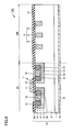
- the silicon carbide semiconductor device according to the present embodiment has an element region IR (active region) and a termination region OR (invalid region) surrounding element region IR.
- Termination region OR includes guard ring region 5. That is, the element region IR is surrounded by the guard ring region 5.
- a semiconductor element 7 such as a transistor or a diode is provided in the element region IR.
- the semiconductor element 7 mainly includes, for example, a silicon carbide semiconductor substrate 10 made of hexagonal silicon carbide, a gate insulating film 15, a gate electrode 17, a source electrode 16, and a drain electrode 19.
- Silicon carbide semiconductor substrate 10 includes a base substrate 1 and an epitaxial layer 2, and epitaxial layer 2 mainly includes a drift region 12, a p body region 13, an n + source region 14, and a p + region 18. .
- the drift region 12 is the epitaxial layer 2 where the p body region 13, the n + source region 14, and the p + region 18 are not formed.
- P body region 13 has p type conductivity.
- P body region 13 is formed in drift region 12 including main surface 2 ⁇ / b> A of silicon carbide semiconductor substrate 10.
- the p-type impurity contained in p body region 13 is, for example, aluminum (Al), boron (B), or the like.
- the impurity concentration of aluminum or the like contained in p body region 13 is, for example, about 1 ⁇ 10 17 cm ⁇ 3 .
- N + source region 14 has n type conductivity.
- N + source region 14 is formed inside p body region 13 so as to include main surface 2 A and be surrounded by p body region 13.
- the n-type impurity contained in the n + source region 14 is, for example, P (phosphorus).
- the concentration of impurities such as phosphorus contained in n + source region 14 is higher than that of n-type impurities contained in drift region 12, for example, about 1 ⁇ 10 20 cm ⁇ 3 .
- the p + region 18 has p type conductivity.
- P + region 18 is formed so as to contact main surface 2A and p body region 13 and penetrate the vicinity of the center of n + source region 14.
- the p + region 18 contains p-type impurities such as Al and B at a higher concentration than the p-type impurities contained in the p body region 13, for example, about 1 ⁇ 10 20 cm ⁇ 3 .
- Gate insulating film 15 is formed in contact with drift region 12 so as to extend from the upper surface of one n + source region 14 to the upper surface of the other n + source region 14.
- the gate insulating film 15 is made of, for example, silicon dioxide (SiO 2 ).
- the gate electrode 17 is disposed in contact with the gate insulating film 15 so as to extend from one n + source region 14 to the other n + source region 14.
- the gate electrode 17 is made of a conductor such as polysilicon or Al.
- Source electrode 16 is disposed in contact with the n + source region 14 and the p + region 18 on the main surface 2A.
- Source electrode 16 includes, for example, titanium (Ti) atoms, Al atoms, and silicon (Si) atoms. Thereby, source electrode 16 can make ohmic contact with both n-type silicon carbide region (n + source region 14) and p-type silicon carbide region (p + region 18).
- the drain electrode 19 is formed in contact with the back surface 1B in the silicon carbide semiconductor substrate 10.
- the drain electrode 19 may have the same configuration as the source electrode 16, for example, and is made of another material capable of ohmic contact with the silicon carbide semiconductor substrate 10 (base substrate 1) such as nickel (Ni). It may be. Thereby, the drain electrode 19 is electrically connected to the base substrate 1.
- the guard ring region 5 has an annular planar shape, and is disposed in the termination region OR of the silicon carbide semiconductor substrate 10 so as to surround the element region IR provided with the semiconductor element 7.
- Guard ring region 5 has p-type (second conductivity type).
- the guard ring region 5 is a conductive region that acts as a guard ring.
- the plurality of guard rings 6 in the guard ring region 5 contain impurities such as boron and aluminum.
- the impurity concentration in each of the plurality of guard rings 6 is lower than the impurity concentration in p body region 13.
- the concentration of the impurity in each of the plurality of guard rings 6 is, for example, 1.3 ⁇ 10 13 cm ⁇ 3 , and preferably about 8 ⁇ 10 12 cm ⁇ 3 to 1.4 ⁇ 10 13 cm ⁇ 3 .
- the method for manufacturing the silicon carbide semiconductor device according to the present embodiment is manufactured using the silicon carbide semiconductor substrate according to the present embodiment.
- silicon carbide semiconductor substrate 10 obtained as described above is prepared (step (S10) to step (S30)).
- impurities are implanted into main surface 2 ⁇ / b> A of silicon carbide semiconductor substrate 10, so that p body region 13, n source region 14, p + region 18, and guard are formed in epitaxial layer 2.
- the ring region 5 is formed (step (S40)).
- Al is ion-implanted as a p-type impurity into epitaxial layer 2 having a conductivity type of n to form p body region 13 having a conductivity type of p type.
- P is ion-implanted as an n-type impurity in p body region 13, thereby forming n source region 14 having an n conductivity type.
- Al is ion-implanted as a p-type impurity, whereby p + region 18 having a p-type conductivity is formed.
- Al is ion-implanted as a p-type impurity, whereby a p-type guard ring region 5 is formed.
- ion implantation in this step (S40) is performed, for example, in a state where the substrate temperature of silicon carbide semiconductor substrate 10 is raised to about 100 ° C. or higher and about 500 ° C.
- warpage of silicon carbide semiconductor substrate 10 is not less than ⁇ 1.5 mm and not more than 1.5 mm. Further, as described above, in the method for manufacturing the silicon carbide semiconductor substrate according to the present embodiment, damaged layer 3 is sufficiently removed by polishing back surface 1B so that the surface roughness (Ra) is 1 nm or less, for example. In this case, the warpage amount of silicon carbide semiconductor substrate 10 can be set to ⁇ 1.0 mm or more and 1.0 mm or less before and after the present step (S40).
- step (S50) heat treatment for activating the impurities added by ion implantation is performed (step (S50)).
- the temperature of the heat treatment is preferably 1500 ° C. or higher and 1900 ° C. or lower, for example, about 1700 ° C.
- the heat treatment time is, for example, about 30 minutes.
- the atmosphere of the heat treatment is preferably an inert gas atmosphere, for example, an argon (Ar) atmosphere.
- the warpage amount of silicon carbide semiconductor substrate 10 is not less than ⁇ 1.5 mm and not more than 1.5 mm.
- damaged layer 3 is sufficiently removed by polishing back surface 1B so that the surface roughness (Ra) is 1 nm or less, for example.
- the warpage amount of silicon carbide semiconductor substrate 10 can be set to ⁇ 1.0 mm or more and 1.0 mm or less before and after performing this step (S50).
- the gate insulating film 15 is formed (step (S60)). Specifically, first, silicon carbide semiconductor substrate 10 on which a desired impurity region is formed is thermally oxidized. Thermal oxidation can be carried out, for example, by heating to about 1300 ° C. in an oxygen atmosphere and holding for about 40 minutes. Thereby, gate insulating film 15 made of SiO 2 is formed on main surface 2A of silicon carbide semiconductor substrate 10.
- the gate electrode 17 is formed (step (S70)).
- a gate electrode 17 made of polysilicon, Al, or the like, which is a conductor extends from one n + source region 14 to the other n + source region 14 and is formed on the gate insulating film 15. Formed to contact.
- polysilicon is adopted as the material of the gate electrode 17, the polysilicon can be contained at a high concentration of P exceeding 1 ⁇ 10 20 cm ⁇ 3 .
- an insulating film made of, for example, SiO 2 is formed so as to cover gate electrode 17.
- an ohmic electrode is formed (step (S80)). Specifically, for example, a resist pattern having an opening that exposes part of p + region 18 and n + source region 14 is formed, and a metal film containing, for example, Si atoms, Ti atoms, and Al atoms Is formed on the entire surface of the substrate.
- the metal film to be an ohmic electrode is formed by, for example, a sputtering method or a vapor deposition method. Thereafter, the resist pattern is lifted off, for example, to form a metal film in contact with the gate insulating film 15 and in contact with the p + region 18 and the n + source region 14.
- the metal film is heated to about 1000 ° C., for example, to form source electrode 16 in ohmic contact with silicon carbide semiconductor substrate 10.
- drain electrode 19 is formed in ohmic contact with n + substrate 11 of silicon carbide semiconductor substrate 10.
- warpage of silicon carbide semiconductor substrate 10 is considered from the viewpoint of the risk of abnormality such as cracking of silicon carbide semiconductor substrate 10.
- the amount is preferably from ⁇ 1.5 mm to 1.5 mm, and more preferably from ⁇ 1.0 mm to 1.0 mm.
- Silicon carbide semiconductor substrate 10 according to the present embodiment has a warpage amount of ⁇ 1.5 mm or more and 1.5 mm or less even when the substrate temperature is heat-treated at a high temperature of about 100 ° C. or more and 500 ° C. or less.
- silicon carbide semiconductor substrate 10 has a warpage amount of ⁇ 1.5 mm or more and 1.5 mm or less even when the substrate temperature is heated to a high temperature of about 200 ° C. or more and 400 ° C. or less. Therefore, it is possible to reduce the risk of occurrence of abnormality such as cracking of silicon carbide semiconductor substrate 10 due to adsorption by the electrostatic chuck stage. Furthermore, silicon carbide semiconductor substrate 10 from which damaged layer 3 has been sufficiently removed has a substrate temperature of about 100 ° C.
- silicon carbide semiconductor substrate 10 from which damaged layer 3 has been sufficiently removed has a substrate temperature of about 200 ° C. to 400 ° C., and the amount of warpage when heated to a high temperature is ⁇ 1.0 mm to 1.0 mm. It is suppressed. Therefore, the risk of occurrence of abnormality such as cracking of silicon carbide semiconductor substrate 10 due to adsorption by the electrostatic chuck stage can be further reduced.
- silicon carbide semiconductor substrate 10 from which damaged layer 3 has been sufficiently removed has a substrate temperature of about 200 ° C. to 400 ° C., and the amount of warpage when heated to a high temperature is ⁇ 1.0 mm to 1.0 mm. It is suppressed. Therefore, the risk of occurrence of abnormality such as cracking of silicon carbide semiconductor substrate 10 due to adsorption by the electrostatic chuck stage can be further reduced.
- the method for manufacturing the silicon carbide semiconductor device according to the present embodiment uses silicon carbide semiconductor substrate 10 having high flatness and high parallelism of main surface 2A, in-plane main surface 2A of silicon carbide semiconductor substrate 10 is used.
- the risk associated with the occurrence of defects such as variations in processing quality can be reduced, and the silicon carbide semiconductor device 100 can be manufactured with high yield.
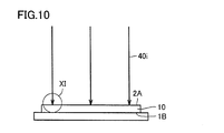
- silicon carbide semiconductor substrate 10 on which step (S40) is performed has a high flatness of main surface 2A.
- the ion implantation angle formed by the implantation direction 40i see FIG. 10
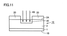
- the variation in the surface of the main surface 2A is kept low. Therefore, referring to FIG.
- impurity implanted region 30 (p body region 13, n source) formed by implanting impurities from the opening of mask film 20 formed on main surface 2A of silicon carbide semiconductor substrate 10. Regions 14 and the like are formed in the same manner in the central portion and the outer peripheral portion of silicon carbide semiconductor substrate 10. From a different point of view, impurity implantation region 30 in silicon carbide semiconductor device 100 has a side wall portion extending in a direction perpendicular to main surface 2A.
- impurity implantation region 30 (p body region 13, n source region 14, etc.) is formed in silicon carbide semiconductor substrate 10 at the center and the outer periphery of silicon carbide semiconductor substrate 10. The position of the area and the way it expands are different.
- impurity implantation region 30 in silicon carbide semiconductor device 100 has a different main surface 2A in the direction in which the side wall portion extends locally with respect to main surface 2A.
- the impurity implantation region 30 having a side wall portion extending perpendicularly to the main surface 2A can be formed. Therefore, there is no problem that the shape of impurity implantation region 30 (for example, the direction in which the side wall extends) differs locally on main surface 2A, so that silicon carbide semiconductor device 100 can be obtained with high yield.
- the step of removing a part of back surface 1B is performed by chemically polishing back surface 1B, but is not limited thereto.
- the step (S30) of removing a part of the back surface 1B may be performed by, for example, reactive ion etching (RIE) of the back surface 1B.
- RIE reactive ion etching
- ICP-RIE Inductive Coupled Plasma-Reactive Ion Etching
- SF 6 or a mixed gas of SF 6 and O 2 as a reaction gas can be used.
- the step of removing a part of the back surface 1B may be performed, for example, by thermally etching the back surface 1B in a halogen gas atmosphere.
- a protective film may be formed on the main surface 2A.
- the protective film may be a thermal oxide film, for example.
- the halogen gas includes, for example, chlorine (Cl 2 ) gas.
- heating of silicon carbide semiconductor substrate 10 may be performed, for example, at about 700 ° C. or more and about 1000 ° C. or less.
- the step of removing a part of the back surface 1B may be performed, for example, by forming a thermal oxide film on the back surface 1B and then etching the thermal oxide film using hydrofluoric acid (HF). . Even in this way, the damage layer 3 can be removed.
- HF hydrofluoric acid
- the silicon carbide semiconductor device according to the present embodiment may have a field stop region (not shown) so as to surround guard ring region 5.
- the field stop region has n-type conductivity, and may be formed by high-temperature implantation in the impurity implantation step (S40) in the same manner as the source region 14 and the like. Since the silicon carbide semiconductor device according to the present embodiment is manufactured using flat silicon carbide semiconductor substrate 10 even under a high temperature environment, the arrangement and form of guard ring region 5 and field stop region are also principal surface 2A. The occurrence of problems such as local fluctuations can be suppressed. Specifically, for example, it is possible to suppress a change in the distance between the guard ring region 5 and the field stop region in the main surface 2A.
- the present invention is particularly advantageously applied to a large-diameter silicon carbide semiconductor substrate having an outer diameter of 100 mm or more, a method for manufacturing the same, and a method for manufacturing a silicon carbide semiconductor device using the silicon carbide semiconductor substrate.
Landscapes
- Recrystallisation Techniques (AREA)
- Crystals, And After-Treatments Of Crystals (AREA)
- Chemical & Material Sciences (AREA)
- Chemical Kinetics & Catalysis (AREA)
- General Chemical & Material Sciences (AREA)
- Physics & Mathematics (AREA)
- Engineering & Computer Science (AREA)
- Plasma & Fusion (AREA)
- Crystallography & Structural Chemistry (AREA)
Abstract
Description
以下、図面を参照して、本発明の実施の形態について説明する。なお、以下の図面において、同一または相当する部分には同一の参照番号を付し、その説明は繰り返さない。また、本明細書中の結晶学的記載においては、個別方位を[]、集合方位を<>、個別面を()、集合面を{}でそれぞれ示している。また結晶学上の指数が負であることは、通常、”-”(バー)を数字の上に付すことによって表現されるが、本明細書中では数字の前に負の符号を付している。
(1)図1を参照して、本実施の形態に係る炭化珪素半導体基板10は、外径が100mm以上である主面2Aを有し、単結晶炭化珪素からなるベース基板1と、主面2A上に形成されたエピタキシャル層2とを備え、基板温度が室温であるときの反り量は-100μm以上100μm以下であり、基板温度が400℃であるときの反り量は-1.5mm以上1.5mm以下である。ここで、図2および図3を参照して、炭化珪素半導体基板10の「反り量」とは、炭化珪素半導体基板10を平面S1に載置したときの、炭化珪素半導体基板10の主面2Aにおいて平面S1に対して最も高い位置と最も低い位置との間の高さの差である。ここで、反り量の正負は、図2を参照して、炭化珪素半導体基板10の主面2Aが下に凸の場合(炭化珪素半導体基板10の中心位置が外周位置よりも平面S1に対して低く位置する場合)をマイナスとし、図3を参照して、上方に凸の場合(炭化珪素半導体基板10の中心位置が外周位置よりも平面S1に対して高く位置する場合)をプラスとする。また、「基板温度」とは、炭化珪素半導体基板10の主面2A側から放射温度計により測定される温度であり、たとえばイオン注入装置などの半導体製造装置において測定される。なお、本実施の形態に係る炭化珪素半導体基板10は、外径が100mm以上の大口径基板であって、好ましくは外径が125mm以上であり、より好ましくは外径が150mm以上である。
次に、本発明の実施の形態の詳細について説明する。
図1を参照して、実施の形態1に係る炭化珪素半導体基板10について説明する。本実施の形態に係る炭化珪素半導体基板10は、ベース基板1と、ベース基板1の主面1A上に形成されたエピタキシャル層2とを備える。
Claims (9)
- 外径が100mm以上である主面を有し、単結晶炭化珪素からなるベース基板と、
前記主面上に形成されたエピタキシャル層とを備え、
基板温度が室温であるときの反り量は-100μm以上100μm以下であり、基板温度が400℃であるときの反り量は-1.5mm以上1.5mm以下である、炭化珪素半導体基板。 - 前記主面に垂直な方向における前記ベース基板の厚みが、200μm以上700μm以下である、請求項1に記載の炭化珪素半導体基板。
- 前記ベース基板において、前記主面の反対側に位置する裏面の表面粗度は10nm以下である、請求項1または請求項2に記載の炭化珪素半導体基板。
- 外径が100mm以上である主面を有し、単結晶炭化珪素からなるベース基板を準備する工程と、
前記主面上にエピタキシャル層を形成する工程と、
前記ベース基板において前記主面の反対側に位置する裏面の少なくとも一部を除去する工程とを備える、炭化珪素半導体基板の製造方法。 - 前記除去する工程は、前記裏面を化学機械研磨することにより行う、請求項4に記載の炭化珪素半導体基板の製造方法。
- 前記除去する工程は、前記裏面を反応性イオンエッチングすることにより行う、請求項4に記載の炭化珪素半導体基板の製造方法。
- 前記除去する工程は、前記裏面をハロゲンガス雰囲気下において熱エッチングすることにより行う、請求項4に記載の炭化珪素半導体基板の製造方法。
- 前記除去する工程は、前記裏面に熱酸化膜を形成した後、前記熱酸化膜をフッ化水素酸を用いてエッチングすることにより行う、請求項4に記載の炭化珪素半導体基板の製造方法。
- 外径が100mm以上である主面を有し、単結晶炭化珪素からなるベース基板を準備する工程と、
前記主面上にエピタキシャル層を形成する工程と、
前記ベース基板において前記主面の反対側に位置する裏面の少なくとも一部を除去して、炭化珪素半導体基板を準備する工程と、
前記炭化珪素半導体基板に不純物イオンを注入する工程とを備える、炭化珪素半導体装置の製造方法。
Priority Applications (3)
| Application Number | Priority Date | Filing Date | Title |
|---|---|---|---|
| US14/910,182 US10050109B2 (en) | 2013-08-06 | 2014-06-13 | Silicon carbide semiconductor substrate, method for manufacturing silicon carbide semiconductor substrate, and method for manufacturing silicon carbide semiconductor device |
| EP14834133.2A EP3035371B1 (en) | 2013-08-06 | 2014-06-13 | Silicon carbide semiconductor substrate, method for producing same, and method for producing silicon carbide semiconductor device |
| CN201480043442.2A CN105453220B (zh) | 2013-08-06 | 2014-06-13 | 碳化硅半导体衬底、制造碳化硅半导体衬底的方法、以及制造碳化硅半导体器件的方法 |
Applications Claiming Priority (2)
| Application Number | Priority Date | Filing Date | Title |
|---|---|---|---|
| JP2013163406A JP6136731B2 (ja) | 2013-08-06 | 2013-08-06 | 炭化珪素半導体基板およびその製造方法、ならびに炭化珪素半導体装置の製造方法 |
| JP2013-163406 | 2013-08-06 |
Publications (1)
| Publication Number | Publication Date |
|---|---|
| WO2015019707A1 true WO2015019707A1 (ja) | 2015-02-12 |
Family
ID=52461050
Family Applications (1)
| Application Number | Title | Priority Date | Filing Date |
|---|---|---|---|
| PCT/JP2014/065712 Ceased WO2015019707A1 (ja) | 2013-08-06 | 2014-06-13 | 炭化珪素半導体基板およびその製造方法、ならびに炭化珪素半導体装置の製造方法 |
Country Status (5)
| Country | Link |
|---|---|
| US (1) | US10050109B2 (ja) |
| EP (1) | EP3035371B1 (ja) |
| JP (1) | JP6136731B2 (ja) |
| CN (2) | CN105453220B (ja) |
| WO (1) | WO2015019707A1 (ja) |
Cited By (1)
| Publication number | Priority date | Publication date | Assignee | Title |
|---|---|---|---|---|
| JP2022172550A (ja) * | 2021-05-06 | 2022-11-17 | 住友電気工業株式会社 | 炭化珪素エピタキシャル基板の製造方法および炭化珪素半導体装置の製造方法 |
Families Citing this family (13)
| Publication number | Priority date | Publication date | Assignee | Title |
|---|---|---|---|---|
| US9716006B2 (en) * | 2014-07-30 | 2017-07-25 | Mitsubishi Electric Corporation | Semiconductor device manufacturing method and semiconductor device |
| US10283595B2 (en) * | 2015-04-10 | 2019-05-07 | Panasonic Corporation | Silicon carbide semiconductor substrate used to form semiconductor epitaxial layer thereon |
| US9978651B2 (en) * | 2015-05-11 | 2018-05-22 | Sumitomo Electric Industries, Ltd. | Silicon carbide single crystal substrate, silicon carbide semiconductor device, and method for manufacturing silicon carbide semiconductor device |
| JP6981505B2 (ja) * | 2015-10-15 | 2021-12-15 | 住友電気工業株式会社 | 炭化珪素エピタキシャル基板の製造方法 |
| JP6964388B2 (ja) * | 2015-10-15 | 2021-11-10 | 住友電気工業株式会社 | 炭化珪素エピタキシャル基板 |
| JP6758491B2 (ja) | 2017-05-17 | 2020-09-23 | 三菱電機株式会社 | SiCエピタキシャルウエハおよびその製造方法 |
| JP7002932B2 (ja) * | 2017-12-22 | 2022-01-20 | 昭和電工株式会社 | SiCインゴットの製造方法 |
| US10879359B2 (en) | 2018-03-02 | 2020-12-29 | National Institute Of Advanced Industrial Science And Technology | Silicon carbide epitaxial wafer having a thick silicon carbide layer with small wrapage and manufacturing method thereof |
| CN118043294A (zh) * | 2021-07-09 | 2024-05-14 | 帕里杜斯有限公司 | SiC P型和低电阻率晶体、晶棒、晶圆和设备及其制造方法 |
| JP2023095359A (ja) * | 2021-12-24 | 2023-07-06 | 株式会社デンソー | 炭化珪素ウェハおよびその製造方法 |
| CN114393512A (zh) * | 2022-01-30 | 2022-04-26 | 北京天科合达半导体股份有限公司 | 一种无损伤层碳化硅晶片表面快速加工的方法 |
| JP7268784B1 (ja) * | 2022-05-31 | 2023-05-08 | 株式会社レゾナック | SiC基板及びSiCエピタキシャルウェハ |
| US12269123B1 (en) | 2024-04-05 | 2025-04-08 | Wolfspeed, Inc. | Laser edge shaping for semiconductor wafers |
Citations (6)
| Publication number | Priority date | Publication date | Assignee | Title |
|---|---|---|---|---|
| JP2007201155A (ja) * | 2006-01-26 | 2007-08-09 | Nissan Motor Co Ltd | 炭化珪素半導体装置及び炭化珪素半導体装置の製造方法 |
| WO2008120467A1 (ja) * | 2007-03-29 | 2008-10-09 | Panasonic Corporation | 半導体装置の製造方法 |
| WO2012049792A1 (ja) * | 2010-10-15 | 2012-04-19 | 三菱電機株式会社 | 炭化珪素半導体素子の製造方法 |
| JP2012214376A (ja) | 2005-04-07 | 2012-11-08 | Cree Inc | 歪み、反り、及びttvが少ない75ミリメートル炭化珪素ウェハ |
| JP2013118213A (ja) * | 2011-12-01 | 2013-06-13 | Showa Denko Kk | 炭化珪素半導体装置及びその製造方法 |
| JP2013128050A (ja) * | 2011-12-19 | 2013-06-27 | Sumitomo Electric Ind Ltd | 半導体装置 |
Family Cites Families (9)
| Publication number | Priority date | Publication date | Assignee | Title |
|---|---|---|---|---|
| US5952679A (en) * | 1996-10-17 | 1999-09-14 | Denso Corporation | Semiconductor substrate and method for straightening warp of semiconductor substrate |
| JP3920103B2 (ja) * | 2002-01-31 | 2007-05-30 | 大阪府 | 絶縁層埋め込み型半導体炭化シリコン基板の製造方法及びその製造装置 |
| US7405430B2 (en) * | 2005-06-10 | 2008-07-29 | Cree, Inc. | Highly uniform group III nitride epitaxial layers on 100 millimeter diameter silicon carbide substrates |
| WO2010119792A1 (ja) * | 2009-04-15 | 2010-10-21 | 住友電気工業株式会社 | 基板、薄膜付き基板、半導体装置、および半導体装置の製造方法 |
| JP2011108809A (ja) * | 2009-11-17 | 2011-06-02 | Bridgestone Corp | 半導体素子の製造方法 |
| JP4887418B2 (ja) * | 2009-12-14 | 2012-02-29 | 昭和電工株式会社 | SiCエピタキシャルウェハの製造方法 |
| GB2484506A (en) * | 2010-10-13 | 2012-04-18 | Univ Warwick | Heterogrowth |
| CN102543718A (zh) * | 2010-12-14 | 2012-07-04 | 北京天科合达蓝光半导体有限公司 | 一种降低碳化硅晶片翘曲度、弯曲度的方法 |
| DE112012003260T5 (de) | 2011-08-05 | 2014-05-15 | Sumitomo Electric Industries, Ltd. | Substrat, Halbleitervorrichtung und Verfahren zur Herstellung derselben |
-
2013
- 2013-08-06 JP JP2013163406A patent/JP6136731B2/ja active Active
-
2014
- 2014-06-13 WO PCT/JP2014/065712 patent/WO2015019707A1/ja not_active Ceased
- 2014-06-13 EP EP14834133.2A patent/EP3035371B1/en active Active
- 2014-06-13 US US14/910,182 patent/US10050109B2/en active Active
- 2014-06-13 CN CN201480043442.2A patent/CN105453220B/zh active Active
- 2014-06-13 CN CN201711098415.7A patent/CN107833829B/zh active Active
Patent Citations (6)
| Publication number | Priority date | Publication date | Assignee | Title |
|---|---|---|---|---|
| JP2012214376A (ja) | 2005-04-07 | 2012-11-08 | Cree Inc | 歪み、反り、及びttvが少ない75ミリメートル炭化珪素ウェハ |
| JP2007201155A (ja) * | 2006-01-26 | 2007-08-09 | Nissan Motor Co Ltd | 炭化珪素半導体装置及び炭化珪素半導体装置の製造方法 |
| WO2008120467A1 (ja) * | 2007-03-29 | 2008-10-09 | Panasonic Corporation | 半導体装置の製造方法 |
| WO2012049792A1 (ja) * | 2010-10-15 | 2012-04-19 | 三菱電機株式会社 | 炭化珪素半導体素子の製造方法 |
| JP2013118213A (ja) * | 2011-12-01 | 2013-06-13 | Showa Denko Kk | 炭化珪素半導体装置及びその製造方法 |
| JP2013128050A (ja) * | 2011-12-19 | 2013-06-27 | Sumitomo Electric Ind Ltd | 半導体装置 |
Non-Patent Citations (1)
| Title |
|---|
| See also references of EP3035371A4 |
Cited By (2)
| Publication number | Priority date | Publication date | Assignee | Title |
|---|---|---|---|---|
| JP2022172550A (ja) * | 2021-05-06 | 2022-11-17 | 住友電気工業株式会社 | 炭化珪素エピタキシャル基板の製造方法および炭化珪素半導体装置の製造方法 |
| JP7661771B2 (ja) | 2021-05-06 | 2025-04-15 | 住友電気工業株式会社 | 炭化珪素エピタキシャル基板の製造方法および炭化珪素半導体装置の製造方法 |
Also Published As
| Publication number | Publication date |
|---|---|
| EP3035371B1 (en) | 2026-04-15 |
| US10050109B2 (en) | 2018-08-14 |
| CN105453220A (zh) | 2016-03-30 |
| CN105453220B (zh) | 2017-11-17 |
| EP3035371A1 (en) | 2016-06-22 |
| EP3035371A4 (en) | 2017-03-22 |
| JP2015032787A (ja) | 2015-02-16 |
| JP6136731B2 (ja) | 2017-05-31 |
| CN107833829B (zh) | 2022-02-18 |
| CN107833829A (zh) | 2018-03-23 |
| US20160181375A1 (en) | 2016-06-23 |
Similar Documents
| Publication | Publication Date | Title |
|---|---|---|
| JP6136731B2 (ja) | 炭化珪素半導体基板およびその製造方法、ならびに炭化珪素半導体装置の製造方法 | |
| JP6197461B2 (ja) | 炭化珪素半導体基板およびその製造方法、ならびに炭化珪素半導体装置の製造方法 | |
| JP6136732B2 (ja) | 炭化珪素半導体基板およびその製造方法、ならびに炭化珪素半導体装置の製造方法 | |
| US20130119406A1 (en) | Silicon carbide substrate, semiconductor device, and methods for manufacturing them | |
| WO2014192411A9 (ja) | 炭化珪素基板および炭化珪素半導体装置ならびに炭化珪素基板および炭化珪素半導体装置の製造方法 | |
| JP2013027960A (ja) | 炭化珪素基板の製造方法および炭化珪素基板 | |
| JP6340642B2 (ja) | 炭化珪素半導体基板およびその製造方法、ならびに炭化珪素半導体装置の製造方法 | |
| KR20110120335A (ko) | 탄화규소 기판의 제조 방법 | |
| JP2017183729A (ja) | 炭化珪素半導体基板およびその製造方法、ならびに炭化珪素半導体装置の製造方法 | |
| JP2017050446A (ja) | 炭化珪素エピタキシャル基板および炭化珪素半導体装置の製造方法 | |
| CN104126218B (zh) | 制造碳化硅半导体器件的方法 | |
| TW201308622A (zh) | 半導體裝置之製造方法 | |
| US20120273800A1 (en) | Composite substrate having single-crystal silicon carbide substrate | |
| WO2019049525A1 (ja) | 炭化珪素エピタキシャル基板および炭化珪素半導体装置の製造方法 | |
| JP6107450B2 (ja) | 炭化珪素半導体装置の製造方法 | |
| JP2016028009A (ja) | 炭化珪素基板および炭化珪素半導体装置ならびに炭化珪素基板および炭化珪素半導体装置の製造方法 |
Legal Events
| Date | Code | Title | Description |
|---|---|---|---|
| WWE | Wipo information: entry into national phase |
Ref document number: 201480043442.2 Country of ref document: CN |
|
| 121 | Ep: the epo has been informed by wipo that ep was designated in this application |
Ref document number: 14834133 Country of ref document: EP Kind code of ref document: A1 |
|
| WWE | Wipo information: entry into national phase |
Ref document number: 2014834133 Country of ref document: EP |
|
| WWE | Wipo information: entry into national phase |
Ref document number: 14910182 Country of ref document: US |
|
| NENP | Non-entry into the national phase |
Ref country code: DE |
|
| WWG | Wipo information: grant in national office |
Ref document number: 2014834133 Country of ref document: EP |