WO2015023034A1 - 조성물, 유기 광전자 소자 및 표시 장치 - Google Patents

조성물, 유기 광전자 소자 및 표시 장치 Download PDF

Info

Publication number
WO2015023034A1
WO2015023034A1 PCT/KR2014/001390 KR2014001390W WO2015023034A1 WO 2015023034 A1 WO2015023034 A1 WO 2015023034A1 KR 2014001390 W KR2014001390 W KR 2014001390W WO 2015023034 A1 WO2015023034 A1 WO 2015023034A1
Authority
WO
WIPO (PCT)
Prior art keywords
formula
substituted
unsubstituted
group
compound
Prior art date
Legal status (The legal status is an assumption and is not a legal conclusion. Google has not performed a legal analysis and makes no representation as to the accuracy of the status listed.)
Ceased
Application number
PCT/KR2014/001390
Other languages
English (en)
French (fr)
Inventor
조영경
이한일
강의수
김윤환
양용탁
오재진
이남헌
류진현
민수현
유은선
정호국
Current Assignee (The listed assignees may be inaccurate. Google has not performed a legal analysis and makes no representation or warranty as to the accuracy of the list.)
Cheil Industries Inc
Original Assignee
Cheil Industries Inc
Priority date (The priority date is an assumption and is not a legal conclusion. Google has not performed a legal analysis and makes no representation as to the accuracy of the date listed.)
Filing date
Publication date
Application filed by Cheil Industries Inc filed Critical Cheil Industries Inc
Priority to CN201480044784.6A priority Critical patent/CN105473684A/zh
Priority to US14/896,547 priority patent/US20160133851A1/en
Priority to JP2016533229A priority patent/JP6409065B2/ja
Priority to EP14836457.3A priority patent/EP3034581B1/en
Publication of WO2015023034A1 publication Critical patent/WO2015023034A1/ko
Anticipated expiration legal-status Critical
Ceased legal-status Critical Current

Links

Classifications

    • HELECTRICITY
    • H10SEMICONDUCTOR DEVICES; ELECTRIC SOLID-STATE DEVICES NOT OTHERWISE PROVIDED FOR
    • H10KORGANIC ELECTRIC SOLID-STATE DEVICES
    • H10K85/00Organic materials used in the body or electrodes of devices covered by this subclass
    • H10K85/60Organic compounds having low molecular weight
    • H10K85/649Aromatic compounds comprising a hetero atom
    • H10K85/657Polycyclic condensed heteroaromatic hydrocarbons
    • CCHEMISTRY; METALLURGY
    • C07ORGANIC CHEMISTRY
    • C07DHETEROCYCLIC COMPOUNDS
    • C07D405/00Heterocyclic compounds containing both one or more hetero rings having oxygen atoms as the only ring hetero atoms, and one or more rings having nitrogen as the only ring hetero atom
    • C07D405/02Heterocyclic compounds containing both one or more hetero rings having oxygen atoms as the only ring hetero atoms, and one or more rings having nitrogen as the only ring hetero atom containing two hetero rings
    • C07D405/04Heterocyclic compounds containing both one or more hetero rings having oxygen atoms as the only ring hetero atoms, and one or more rings having nitrogen as the only ring hetero atom containing two hetero rings directly linked by a ring-member-to-ring-member bond
    • CCHEMISTRY; METALLURGY
    • C07ORGANIC CHEMISTRY
    • C07DHETEROCYCLIC COMPOUNDS
    • C07D409/00Heterocyclic compounds containing two or more hetero rings, at least one ring having sulfur atoms as the only ring hetero atoms
    • C07D409/02Heterocyclic compounds containing two or more hetero rings, at least one ring having sulfur atoms as the only ring hetero atoms containing two hetero rings
    • C07D409/04Heterocyclic compounds containing two or more hetero rings, at least one ring having sulfur atoms as the only ring hetero atoms containing two hetero rings directly linked by a ring-member-to-ring-member bond
    • CCHEMISTRY; METALLURGY
    • C09DYES; PAINTS; POLISHES; NATURAL RESINS; ADHESIVES; COMPOSITIONS NOT OTHERWISE PROVIDED FOR; APPLICATIONS OF MATERIALS NOT OTHERWISE PROVIDED FOR
    • C09KMATERIALS FOR MISCELLANEOUS APPLICATIONS, NOT PROVIDED FOR ELSEWHERE
    • C09K11/00Luminescent materials, e.g. electroluminescent or chemiluminescent
    • C09K11/02Use of particular materials as binders, particle coatings or suspension media therefor
    • C09K11/025Use of particular materials as binders, particle coatings or suspension media therefor non-luminescent particle coatings or suspension media
    • HELECTRICITY
    • H10SEMICONDUCTOR DEVICES; ELECTRIC SOLID-STATE DEVICES NOT OTHERWISE PROVIDED FOR
    • H10KORGANIC ELECTRIC SOLID-STATE DEVICES
    • H10K50/00Organic light-emitting devices
    • H10K50/10OLEDs or polymer light-emitting diodes [PLED]
    • H10K50/11OLEDs or polymer light-emitting diodes [PLED] characterised by the electroluminescent [EL] layers
    • HELECTRICITY
    • H10SEMICONDUCTOR DEVICES; ELECTRIC SOLID-STATE DEVICES NOT OTHERWISE PROVIDED FOR
    • H10KORGANIC ELECTRIC SOLID-STATE DEVICES
    • H10K59/00Integrated devices, or assemblies of multiple devices, comprising at least one organic light-emitting element covered by group H10K50/00
    • H10K59/30Devices specially adapted for multicolour light emission
    • H10K59/32Stacked devices having two or more layers, each emitting at different wavelengths
    • HELECTRICITY
    • H10SEMICONDUCTOR DEVICES; ELECTRIC SOLID-STATE DEVICES NOT OTHERWISE PROVIDED FOR
    • H10KORGANIC ELECTRIC SOLID-STATE DEVICES
    • H10K85/00Organic materials used in the body or electrodes of devices covered by this subclass
    • H10K85/60Organic compounds having low molecular weight
    • H10K85/615Polycyclic condensed aromatic hydrocarbons, e.g. anthracene
    • H10K85/622Polycyclic condensed aromatic hydrocarbons, e.g. anthracene containing four rings, e.g. pyrene
    • HELECTRICITY
    • H10SEMICONDUCTOR DEVICES; ELECTRIC SOLID-STATE DEVICES NOT OTHERWISE PROVIDED FOR
    • H10KORGANIC ELECTRIC SOLID-STATE DEVICES
    • H10K85/00Organic materials used in the body or electrodes of devices covered by this subclass
    • H10K85/60Organic compounds having low molecular weight
    • H10K85/615Polycyclic condensed aromatic hydrocarbons, e.g. anthracene
    • H10K85/623Polycyclic condensed aromatic hydrocarbons, e.g. anthracene containing five rings, e.g. pentacene
    • HELECTRICITY
    • H10SEMICONDUCTOR DEVICES; ELECTRIC SOLID-STATE DEVICES NOT OTHERWISE PROVIDED FOR
    • H10KORGANIC ELECTRIC SOLID-STATE DEVICES
    • H10K85/00Organic materials used in the body or electrodes of devices covered by this subclass
    • H10K85/60Organic compounds having low molecular weight
    • H10K85/631Amine compounds having at least two aryl rest on at least one amine-nitrogen atom, e.g. triphenylamine
    • HELECTRICITY
    • H10SEMICONDUCTOR DEVICES; ELECTRIC SOLID-STATE DEVICES NOT OTHERWISE PROVIDED FOR
    • H10KORGANIC ELECTRIC SOLID-STATE DEVICES
    • H10K85/00Organic materials used in the body or electrodes of devices covered by this subclass
    • H10K85/60Organic compounds having low molecular weight
    • H10K85/649Aromatic compounds comprising a hetero atom
    • HELECTRICITY
    • H10SEMICONDUCTOR DEVICES; ELECTRIC SOLID-STATE DEVICES NOT OTHERWISE PROVIDED FOR
    • H10KORGANIC ELECTRIC SOLID-STATE DEVICES
    • H10K85/00Organic materials used in the body or electrodes of devices covered by this subclass
    • H10K85/60Organic compounds having low molecular weight
    • H10K85/649Aromatic compounds comprising a hetero atom
    • H10K85/654Aromatic compounds comprising a hetero atom comprising only nitrogen as heteroatom
    • HELECTRICITY
    • H10SEMICONDUCTOR DEVICES; ELECTRIC SOLID-STATE DEVICES NOT OTHERWISE PROVIDED FOR
    • H10KORGANIC ELECTRIC SOLID-STATE DEVICES
    • H10K85/00Organic materials used in the body or electrodes of devices covered by this subclass
    • H10K85/60Organic compounds having low molecular weight
    • H10K85/649Aromatic compounds comprising a hetero atom
    • H10K85/657Polycyclic condensed heteroaromatic hydrocarbons
    • H10K85/6572Polycyclic condensed heteroaromatic hydrocarbons comprising only nitrogen in the heteroaromatic polycondensed ring system, e.g. phenanthroline or carbazole
    • HELECTRICITY
    • H10SEMICONDUCTOR DEVICES; ELECTRIC SOLID-STATE DEVICES NOT OTHERWISE PROVIDED FOR
    • H10KORGANIC ELECTRIC SOLID-STATE DEVICES
    • H10K85/00Organic materials used in the body or electrodes of devices covered by this subclass
    • H10K85/60Organic compounds having low molecular weight
    • H10K85/649Aromatic compounds comprising a hetero atom
    • H10K85/657Polycyclic condensed heteroaromatic hydrocarbons
    • H10K85/6574Polycyclic condensed heteroaromatic hydrocarbons comprising only oxygen in the heteroaromatic polycondensed ring system, e.g. cumarine dyes
    • HELECTRICITY
    • H10SEMICONDUCTOR DEVICES; ELECTRIC SOLID-STATE DEVICES NOT OTHERWISE PROVIDED FOR
    • H10KORGANIC ELECTRIC SOLID-STATE DEVICES
    • H10K85/00Organic materials used in the body or electrodes of devices covered by this subclass
    • H10K85/60Organic compounds having low molecular weight
    • H10K85/649Aromatic compounds comprising a hetero atom
    • H10K85/657Polycyclic condensed heteroaromatic hydrocarbons
    • H10K85/6576Polycyclic condensed heteroaromatic hydrocarbons comprising only sulfur in the heteroaromatic polycondensed ring system, e.g. benzothiophene
    • HELECTRICITY
    • H10SEMICONDUCTOR DEVICES; ELECTRIC SOLID-STATE DEVICES NOT OTHERWISE PROVIDED FOR
    • H10KORGANIC ELECTRIC SOLID-STATE DEVICES
    • H10K2101/00Properties of the organic materials covered by group H10K85/00
    • H10K2101/10Triplet emission
    • HELECTRICITY
    • H10SEMICONDUCTOR DEVICES; ELECTRIC SOLID-STATE DEVICES NOT OTHERWISE PROVIDED FOR
    • H10KORGANIC ELECTRIC SOLID-STATE DEVICES
    • H10K2101/00Properties of the organic materials covered by group H10K85/00
    • H10K2101/90Multiple hosts in the emissive layer

Definitions

  • compositions organic optoelectronic devices and displays.
  • a composition an organic optoelectronic device, and a display device.
  • An organic optoelectric diode is a device capable of converting electrical energy and light energy.
  • Organic optoelectronic devices can be divided into two types according to the principle of operation.
  • Examples of the organic optoelectronic device may be an organic photoelectric device, an organic light emitting device, an organic solar cell and an organic photo conductor drum.
  • organic light emitting diodes converts electrical energy into light by applying an electric current to the organic light emitting material.
  • the organic light emitting device has a structure in which an organic layer is inserted between an anode and a cathode.
  • the organic charge may include a light emitting layer and an auxiliary layer, and the auxiliary layer may include, for example, a hole injection layer, a hole transport layer, an electron blocking layer, an electron transport layer, and an electron injection layer to increase efficiency and stability of the organic light emitting diode. And at least one layer selected from a hole blocking layer.
  • the performance of the organic light emitting device is greatly influenced by the characteristics of the organic layer, and in particular, is affected by the organic material included in the organic layer.
  • One embodiment provides a composition for an organic optoelectronic device capable of implementing high efficiency and long life organic optoelectronic devices.
  • Another embodiment provides an organic optoelectronic device comprising the composition.
  • Another embodiment provides a display device including the organic optoelectronic device.
  • composition comprising a first host compound represented by Formula I and a second host compound represented by Formula II.
  • 3 ⁇ 4 is 0, Se, S, SO, S0 2 , PO or CO,
  • X 2 is CR a R b or SiRcR d ,
  • Ri to R 5 and R a to R d are each independently hydrogen, deuterium, a substituted or unsubstituted C1 to C30 alkyl group, a substituted or unsubstituted C3 to C30 cycloalkyl group, a substituted or unsubstituted C3 to C30 heterocycloalkyl group, Substituted or unsubstituted C6 to C30 aryl group, substituted or unsubstituted C3 to C30 heteroaryl group, substituted or unsubstituted amine group, substituted or unsubstituted C6 to C30 arylamine group, substituted or unsubstituted C3 to C30 heteroarylamine group, substituted or unsubstituted C1 to C30 alkoxy group, substituted or unsubstituted C2 to C30 alkoxycarbonyl group, substituted or unsubstituted C2 to C30 alkoxycarbonylamino group, substituted or unsub
  • Sulfamoylamino groups substituted or unsubstituted C2 to C30 alkenyl groups, substituted or unsubstituted C2 to C30 alkynyl groups, substituted or unsubstituted silyl groups, substituted or unsubstituted silyloxy groups, substituted or unsubstituted C1 to C30 acyl group, substituted or unsubstituted C1 to C20 acyloxy group, substituted or unsubstituted C1 to C20
  • Heterocyclothio group substituted or unsubstituted C6 to C30 arylthi group, substituted or unsubstituted C1 to C30 heteroarylthiol group, substituted or unsubstituted C1 to C30 ureide group, halogen group, halogen-containing group, No group, a hydroxyl group, an amino group, a nitro group carboxyl group, a ferrocenyl group, or a combination thereof.
  • 3 ⁇ 4 is 0, S, CR U R V , SiR w R x or NR y ,
  • HTU is a substituted or unsubstituted carbazolyl group or a substituted or unsubstituted triphenylenyl group
  • Rll to R 13 and R u to R y are each independently hydrogen, deuterium, a substituted or unsubstituted C1 to C20 alkyl group, a substituted or unsubstituted C6 to C30 aryl group, a substituted or unsubstituted C3 to C30 heteroaryl group Or a combination thereof.
  • an organic optoelectronic device comprising an anode and a cathode facing each other, at least one organic layer positioned between the anode and the cathode, the organic layer comprising the composition.
  • a display device including the organic optoelectronic device is provided.
  • FIG. 1 and 2 are cross-sectional views illustrating organic light emitting diodes according to example embodiments.
  • substituted at least one hydrogen of a substituent or a compound is a deuterium, a halogen group, a hydroxy group, an amino group, a substituted or unsubstituted C1 to C30 amine group, a nitro group, a substituted or unsubstituted C1 to C40 silyl group, C1 to C30 alkyl group, C1 to C10 alkylsilyl group, C3 to C30 cycloalkyl group, C3 to C30 heterocycloalkyl group, C6 to C30 aryl group, C6 to C30 aryl group, C6 to C30
  • C1-C10 trifluoroalkyl group or cyano group such as a heteroaryl group, a C1-C20 alkoxy group, a fluoro group, and a trifluoromethyl group.
  • C1 to C10 such as a C20 alkoxy group, a fluoro group, and a trifluoromethyl group
  • Two adjacent substituents of the trifluoroalkyl group or the cyano group may be fused to form a ring.
  • the substituted C6 to C30 aryl group may be fused to another adjacent substituted C6 to C30 aryl group to form a substituted or unsubstituted fluorene ring.
  • hetero means containing one to three heteroatoms selected from the group consisting of N, 0, S, P, and Si in one functional group, and the rest are carbon. .
  • an "alkyl group” is aliphatic
  • the alkyl group may be a "saturated alkyl group" which does not contain any double bonds or triple bonds.
  • the alkyl group may be an alkyl group of C1 to C30. More specifically, the alkyl group may be a C1 to C20 alkyl group or a C1 to C10 alkyl group.
  • a C1 to C4 alkyl group means that the alkyl chain contains 1 to 4 carbon atoms, with methyl, ethyl, propyl, iso-propyl, ⁇ -butyl, iso-butyl, sec -butyl and t-butyl Selected from the group consisting of:
  • alkyl group examples include methyl group, ethyl group, propyl group, isopropyl group, butyl group, isobutyl group, t-butyl group, pentyl group, nuclear group, cyclopropyl group, cyclobutyl group, A cyclopentyl group, a cyclonuclear group, etc. mean.
  • an "aryl group” refers to a substituent in which all elements of a cyclic substituent have a p-orbital, and these P-orbitals form a conjugate, and are monocyclic, polycyclic or Fused ring polycyclic (ie, rings that divide adjacent pairs of carbon atoms) functional groups.
  • heteroaryl group means containing 1 to 3 heteroatoms selected from the group consisting of N, 0, S, P, and Si in the aryl group, and the rest is carbon.
  • heteroaryl group is a fused ring, each ring may include 1 to 3 heteroatoms.
  • a substituted or unsubstituted C6 to C30 aryl group and / or a substituted or unsubstituted C2 to C30 heteroaryl group is a substituted or unsubstituted phenyl group, a substituted or unsubstituted naphthyl group, a substituted or unsubstituted anthra Senyl group, substituted or unsubstituted phenanthryl group, substituted or unsubstituted naphthacenyl group, substituted or unsubstituted pyrenyl group, substituted or unsubstituted biphenyl group, substituted or unsubstituted P-terphenyl group, substituted or unsubstituted A substituted tn-terphenyl group, a substituted or unsubstituted chrysenyl group, a substituted or unsubstituted triphenylenyl group, a substituted or unsubsti
  • Naphthyridinyl groups substituted or unsubstituted benzoxazinyl groups, substituted or unsubstituted benzthiazinyl groups, substituted or unsubstituted acridinyl groups, substituted or unsubstituted phenazineyl groups, substituted or unsubstituted phenothiazines Diary, Substituted or Unsubstituted
  • Phenoxazinyl substituted or unsubstituted fluorenyl groups, substituted or unsubstituted It may be, but is not limited to, a dibenzofuranyl group, a substituted or unsubstituted dibenzothiophenyl group, a substituted or unsubstituted carbazole group, or a combination thereof.
  • the hole characteristic refers to a characteristic capable of forming holes by donating electrons when an electric field is applied, and injecting holes formed at the anode into the light emitting layer having conductive properties along the HOMO level, and emitting layer. It refers to a property that facilitates the movement of the hole formed in the anode and movement in the light emitting layer.
  • the electron characteristic refers to a characteristic that can receive electrons when an electric field is applied, and has a conductivity characteristic along the LUMO level, and injects electrons formed in the cathode into the light emitting layer, moves electrons formed in the light emitting layer to the cathode, and It means a property that facilitates movement.
  • the dopant includes a dopant, and the host includes a first host compound having bipolar characteristics and a second host compound having hole characteristics and having at least two fused rings.
  • the first host compound is represented by the following formula (I).
  • Xi is 0, Se, S, SO, S0 2 , PO or CO,
  • X 2 is CR a R b or SiRcR d ,
  • Ri to R 5 and R a to R d are each independently hydrogen, deuterium, a substituted or unsubstituted C 1 to C30 alkyl group, a substituted or unsubstituted C3 to C30 cycloalkyl group, or a substituted or unsubstituted C3 to C30 heterocycloalkyl group , Substituted or unsubstituted C6 to C30 aryl group, substituted or unsubstituted C3 internal C30 heteroaryl group, substituted or unsubstituted amine group, substituted or unsubstituted C6 to C30 arylamine group, substituted or Unsubstituted C3 to C30 heteroarylamine group, substituted or unsubstituted C1 to C30 alkoxy group, substituted or unsubstituted C2 to C30 alkoxycarbonyl group, substituted or unsubstituted C2 to C30 alkoxycarbonylamino group, substituted or
  • Sulfamoylamino groups substituted or unsubstituted C2 to C30 alkenyl groups, substituted or unsubstituted C2 to C30 alkynyl groups, substituted or unsubstituted silyl groups, substituted or unsubstituted silyloxy groups, substituted or unsubstituted C1 to C30 acyl group, substituted or unsubstituted C1 to C20 acyloxy group, substituted or unsubstituted C1 to C20
  • Heterocyclothiyl group substituted or unsubstituted C6 to C30 arylthiol group, substituted or unsubstituted C1 to C30 heteroarylthi group, substituted or unsubstituted C1 to C30 ureide group, halogen group, halogen-containing group, cya A no group, a hydroxyl group, an amino group, a nitro group, a carboxyl group, a ferrocenyl group, or a combination thereof.
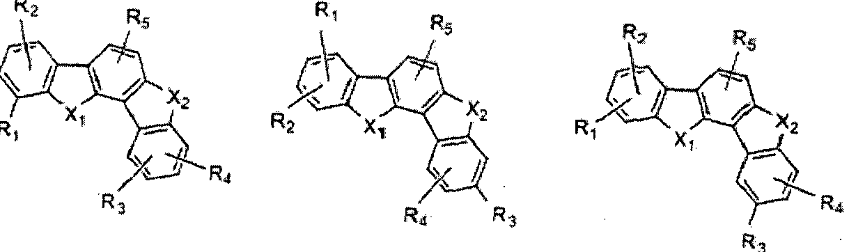
  • the first host compound may be, for example represented by any one of the following formula la to lc depending on the bonding position of the substituent.
  • the first host compound may be represented by any one of the following Formulas 1-1 to 1-6.
  • Ri naeja 3 ⁇ 4 is as described above, such as 3 ⁇ 4 to R 5 are each 'independently represent hydrogen, increased from hydrogen, substituted or unsubstituted C1 to C20 alkyl group, a substituted or unsubstituted C6 to C30 aryl group, a substituted or unsubstituted It may be a ring C3 to C30 heteroaryl group or a combination thereof.
  • At least one of Chemical Formula I, Chemical Formulas la to lc, and Chemical Formulas 1-1 to 1-6 to R 5 and a to Rd may be a substituent having a hole property or an electronic property, for example, substituted or unsubstituted Group 1 It may be one selected from the functional groups listed in.
  • Y is N, 0, S, S0 2 , NRj, CR k , SiR b CR m R n or SiRoR p ,
  • Z is N, CR q , CR r R s or NR t ,
  • R j to R t are each independently hydrogen, deuterium, a substituted or unsubstituted C1 to C20 alkyl group, a substituted or unsubstituted C6 to C30 aryl group, a substituted or unsubstituted C3 to C30 heteroaryl group, or a combination thereof
  • Ar5 is a single bond, a substituted or unsubstituted C1 to C20 alkylene group, a substituted or unsubstituted C2 to C20 alkenylene group, a substituted or unsubstituted C6 to C30 arylene group, a substituted or unsubstituted C2 to C30 heteroarylene group , A substituted or unsubstituted C6 to C30 arylamine group, a substituted or unsubstituted C2 to C30 heteroarylamine group, or a combination thereof,
  • Ar6 and Ar7 are each independently a substituted or unsubstituted C6 to C30 aryl group, a substituted or unsubstituted C3 to C30 heteroaryl group or a combination thereof,
  • nl and n2 are each independently 0 or 1
  • Substituted or unsubstituted functional groups listed in Group 1 may be, for example, one selected from Formulas B-1 to B-35.
  • the first host compound may be represented by, for example, [Table 1] and [Table 2], wherein the substituent means ⁇ when the core parts are 1-1 and 1-2, and the core parts are 1-3 to 1-6.
  • the substituents unless otherwise specified are all hydrogen.
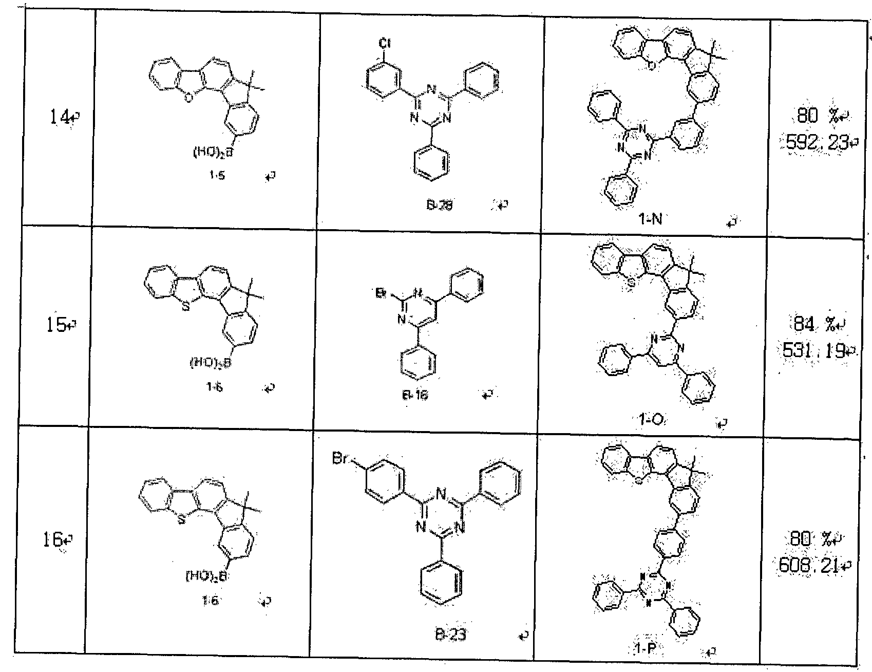
  • the crab 1 host compound may be, for example represented by any one of the following Formula to 1-P.
  • the second host compound is represented by the following formula ( ⁇ ).
  • X 3 is 0, S, CR u Rv, SiR w R x or NR y ,
  • HTU is a substituted or unsubstituted carbazolyl group or a substituted or unsubstituted
  • Rii to R 13 and R u to R y are each independently hydrogen, deuterium, a substituted or unsubstituted C1 to C20 alkyl group, a substituted or unsubstituted C6 to C30 aryl group, a substituted or unsubstituted C3 to C30 heteroaryl group Or a combination thereof.
  • the second host compound may be, for example, a compound represented by Chemical Formula 2 including two carbazole groups.
  • Ar, Ar 2 and Ru to R 16 are as defined in the above to R 5 , for example, Ar Ar 2 and R u to R 16 are each independently hydrogen, deuterium, a substituted or unsubstituted C1 to C20 alkyl group, Or a substituted or unsubstituted C6 to C30 aryl group, a substituted or unsubstituted C3 to C30 heteroaryl group, or a combination thereof.
  • the compound represented by Chemical Formula 2 may be, for example represented by any one of the following Chemical Formulas 2-1 to 2-3 depending on the binding position.
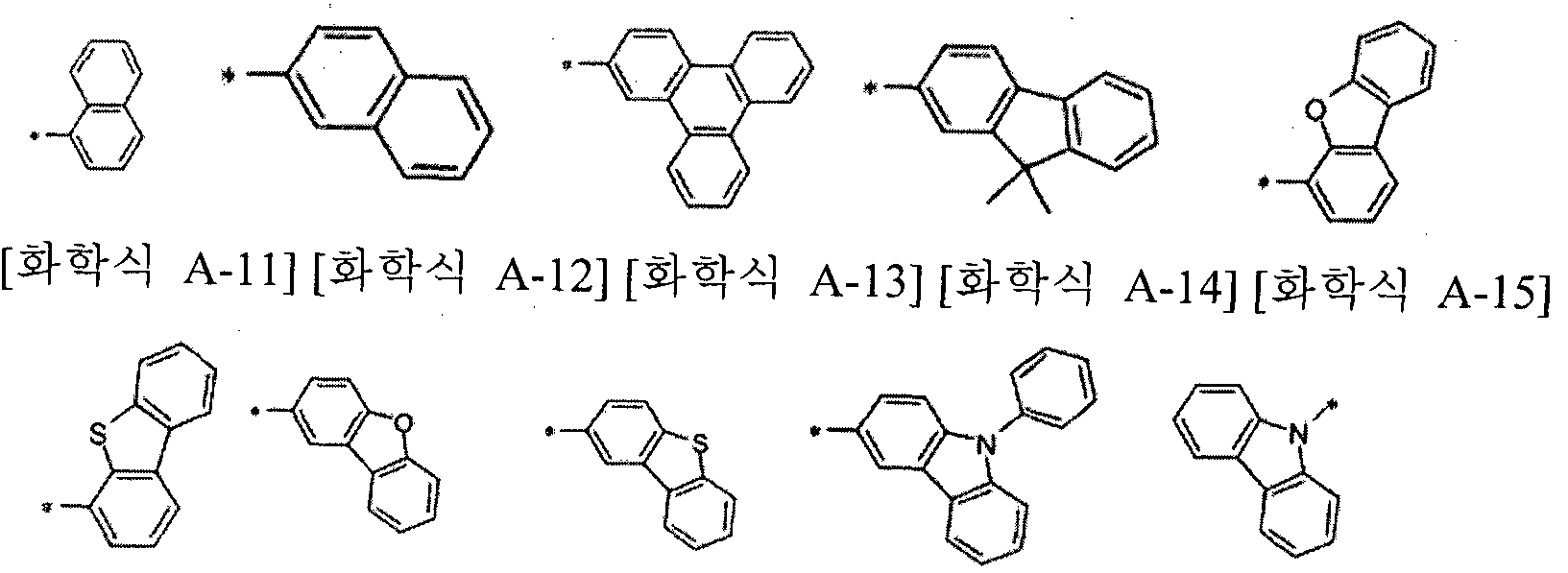
  • A, Ar 2 and R n to R 16 are the same as described above. At least one of the formula 2 and the formula 2-1 to 2-3 ⁇ , ⁇ ⁇ 2 and Ru to R 16 may be a substituent having a hole characteristics, such as the following formulas A-1 to It may be a substituent selected from A-15.
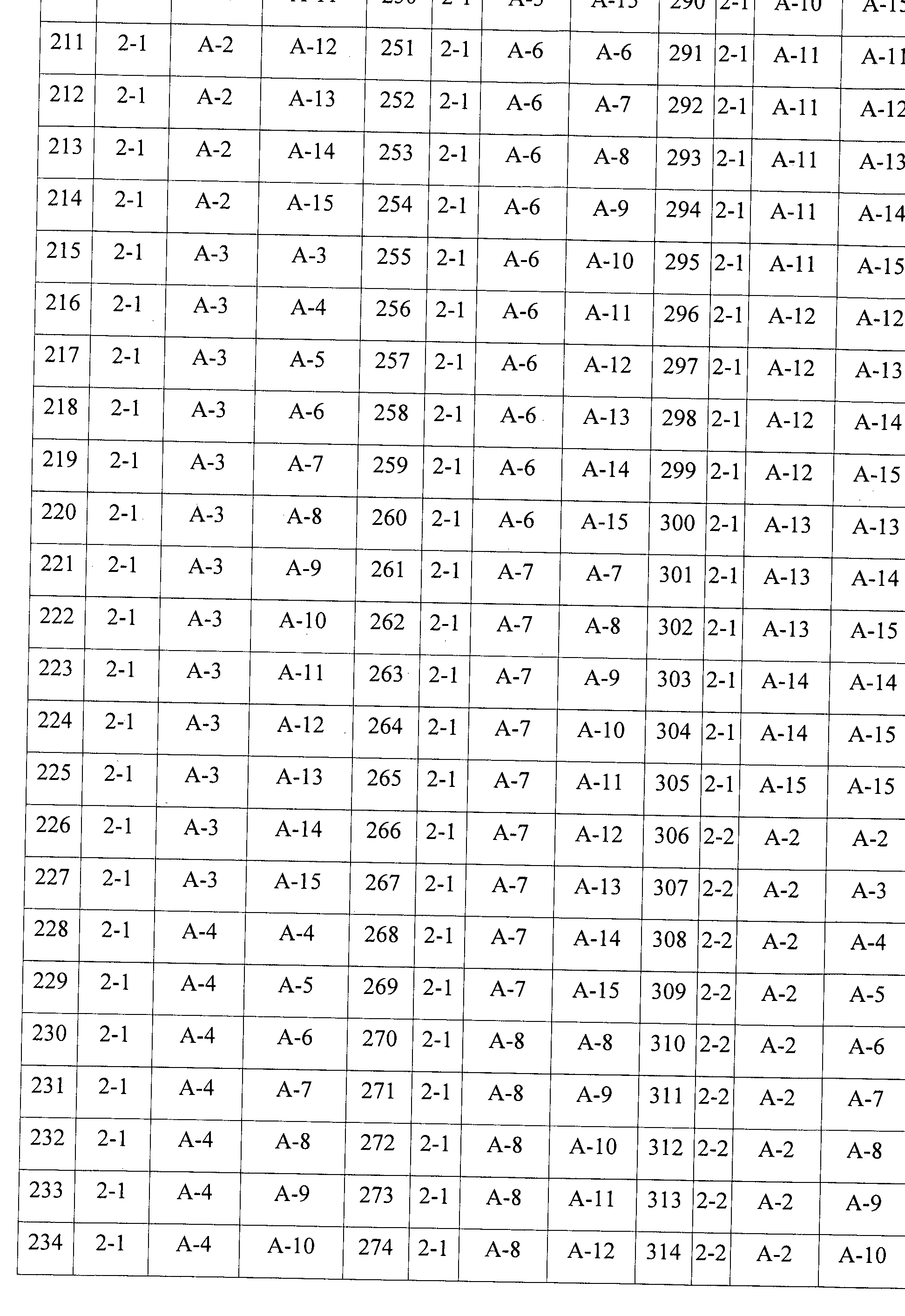
  • the compound represented by Chemical Formula 2 may be represented by, for example, [Table 3] to [Table 5], and the substituents R u to R 16 which are not mentioned here are all hydrogen.
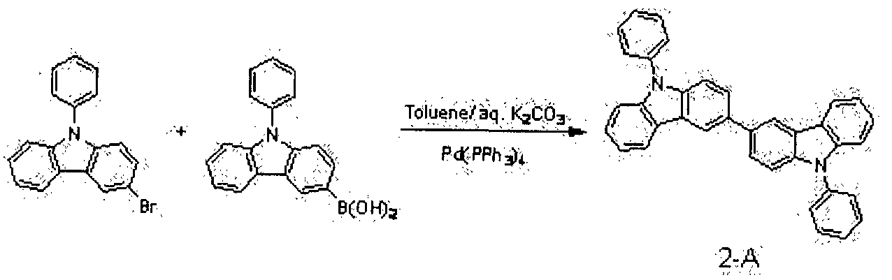
  • the compound represented by Chemical Formula 2 may be, for example, represented by Chemical Formulas 2-A to 2-C.
  • the second host compound may be, for example, a compound represented by Formula 3 below. [Formula 3]
  • X 3 is 0, S, CR e R f , SiR g R h or ⁇ 3 ⁇ 4,
  • L is a single bond, a substituted or unsubstituted C1 to C20 alkylene group, a substituted or unsubstituted C2 to C20 alkenylene group, a substituted or unsubstituted C6 to C30 arylene group, a substituted or unsubstituted C2 to C30 heteroarylene group Or a combination thereof,
  • Ru to R 13 , R 17 to R 21 and R e to R are each independently hydrogen, deuterium : a substituted or unsubstituted C1 to C20 alkyl group, a substituted or unsubstituted C6 to C30 aryl group, a substituted or unsubstituted C3 to C30 heteroaryl group or a combination thereof.
  • the compound represented by Chemical Formula 3 may be represented by, for example, the following Chemical Formula 3a depending on the binding position.
  • the compound represented by Chemical Formula 3 may be, for example represented by any one of the following Chemical Formulas 3-1 to 3-10
  • R u to R 13 , R 17 to R 21, and 3 ⁇ 4 are as described above.
  • At least one of 3 ⁇ 4 ⁇ and 3 ⁇ 4 may be a substituent having a hole, for example, the substituent selected from Chemical Formulas A-1 to A-15.
  • the compound represented by the formula (3) may be represented by, for example, [Table 6] and [Representation, wherein the substituent means R lt when the core portion is 3-1 to 3-8, the core portion 3-9 and 3-10 In the case of R i , and the substituents unless otherwise specified are all hydrogen.
  • the compound represented by Chemical Formula 3 may be, for example represented by one of the following Chemical Formulas 3-A to 3-E.
  • the first host compound and the second host compound may prepare various compositions by various combinations.
  • the composition may include a composition including the first host compound and the second host compound represented by Formula 2, and a composition including the first host compound and the third host compound represented by Formula 3.
  • a compound selected from the compounds of formula (I) shown in Tables 1 and 2 as a first host, the compound of formula (2) shown in Tables 3 to 5, or the compound of Formula (3) shown in Tables 6 and 7 It may be a composition having a second host.
  • the first host compound is a compound having electronic properties and the second host compound is a compound having hole properties
  • bipolar properties may be realized by including them together. Therefore, when the composition is applied to the light emitting layer of the organic optoelectronic device, it is possible to improve good interfacial properties and the ability to transport holes and electrons.
  • the first host compound and the second host compound are, for example, from 1: 10 to It may be included in a weight ratio of 10: 1.
  • the first host compound and the second host compound are, for example, from 1: 10 to It may be included in a weight ratio of 10: 1.
  • composition may further include one or more host compounds in addition to the first host compound and the second host compound described above.
  • the composition may further comprise a dopant.
  • the dopant may be a red, green or blue dopant, for example, a phosphorescent dopant.
  • the dopant is a substance mixed with the first host compound and the second host compound in a small amount to emit light, and is generally a metal complex that emits light by multiple excitation which excites above a triplet state. Materials such as may be used.
  • the dopant may be, for example, an inorganic, organic, or inorganic compound, and may be included in one kind or two or more kinds.
  • the phosphorescent dopant examples include an organometallic compound including Ir, Pt, Os, Ti, Zr, Hf, Eu, Tb, Tm, Fe, Co, Ni, Ru, Rh, Pd, or a combination thereof.
  • the phosphorescent dopant may be a compound represented by the following Chemical Formulas A to C, but is not limited thereto.
  • the composition may be formed by a dry film forming method such as chemical vapor deposition.
  • a dry film forming method such as chemical vapor deposition.
  • the organic optoelectronic device is not particularly limited as long as the device can switch electrical energy and light energy. Examples thereof include an organic photoelectric device, an organic light emitting device, an organic solar cell, and an organic photosensitive drum.
  • 1 and 2 are cross-sectional views illustrating an organic light emitting diode according to an embodiment. Degree. Referring to 1, the organic optoelectronic device 100 according to an embodiment
  • the anode 120 may be made of a high work function conductor, for example, to facilitate hole injection, and may be made of metal, metal oxide, and / or conductive polymer, for example.
  • the anode 120 is, for example, a metal such as nickel, platinum, vanadium, cream, copper, zinc, gold or an alloy thereof; Zinc oxide, indium oxide, indium tin oxide ( ⁇ ),
  • Metal oxides such as indium zinc oxide (IZO); Combinations of oxides with metals such as ZnO and A1 or Sn0 2 and Sb; Conductive polymers such as poly (3-methylthiophene), poly (3,4- (ethylene-1,2-dioxy) thiophene Xpolyehtylenedioxythiophene (PEDT), polypyrrole and polyaniline, and the like, but are not limited thereto. .
  • the cathode 1 10 may be made of a low work function conductor, for example, to facilitate electron injection, and may be made of metal, metal oxide and / or conductive polymer, for example.
  • Cathode 110 is, for example, a metal such as magnesium, calcium, sodium, potassium, titanium, indium, yttrium, lithium, gadolinium, aluminum, silver, tin, lead, cesium, barium, or an alloy thereof; Multilayer structure materials such as LiF / Al, Li0 2 / Al, LiF / Ca, LiF / Al, and BaF 2 / Ca, but are not limited thereto.
  • the organic layer 105 includes a light emitting layer 130 comprising the composition described above.
  • Luminescent 130 may, for example, comprise the composition described above.
  • the organic light emitting diode 200 may have holes in addition to the light emitting layer 130.
  • the hole auxiliary layer 140 may further increase hole injection and / or hole mobility between the anode 120 and the light emitting layer 130 and block electrons.
  • the hole auxiliary layer 140 may be, for example, a hole transport layer, a hole injection layer, and / or an electron blocking layer : and may include at least one layer.
  • FIG. 1 In addition, in one embodiment of the present invention in FIG. 1
  • the organic thin film layer 105 may further be an organic light emitting device further including an electron transport layer, an electron injection layer, a major injection layer, and the like.
  • the organic light emitting diodes 100 and 200 form an anode or a cathode on a substrate, and then form an organic layer by a dry film method such as evaporation, sputtering, plasma plating, and ion plating.
  • a dry film method such as evaporation, sputtering, plasma plating, and ion plating.
  • the organic light emitting diode described above may be applied to an organic light emitting diode display.
  • AHA presents specific embodiments of the present invention. However, the embodiments described below are merely for illustrating or explaining the present invention in detail, and thus the present invention is not limited thereto.
  • the product was purified by silica gel column chromatography with n ⁇ nucleic acid / dichloromethane (7: 3 volume ratio) to give 31 g of the target compound intermediate (A) as a white solid (yield). 94.5%) was obtained.
  • the intermediate (B) was dissolved in 250 ml of dichloromethane and then cooled to 0 ° C and stirred. 12.84 g (47.5 mmol) of borontrifluoride and diethyl ether complex dissolved in 20 mL of dichloromethane were slowly added thereto, followed by stirring at room temperature for 5 hours. After completion of reaction, the mixture was extracted with ethyl acetate, and the extract was dried over magnesium sulphate, filtered, and the filtrate was concentrated under reduced pressure.
  • the product was purified by silica gel column chromatography with n-Hexane to give 22 g (yield 7L9%) of the target compound intermediate (C) as a white solid.
  • the product was purified by a silica gel filter to give 62.5 g of intermediate 1-1 as a target compound. 77%) was obtained.
  • the product was purified by silica gel column chromatography with n-nucleic acid / dichloromethane (7: 3 volume ratio) to give 31 g (yield 88.8%) of the target compound intermediate (D) as a white solid.
  • the intermediate (E) was dissolved 250 m in dichloromethane, and stirred at 0 ° C. Borontrifluoride and diethyl ether complex 12.6 g (47.1 mmol) dissolved in 20 mL of dichloromethane were slowly added thereto, followed by stirring at room temperature for 5 hours. After completion of reaction, the mixture was extracted with ethyl acetate, and the extract was dried over magnesium sulphate, filtered, and the filtrate was concentrated under reduced pressure.
  • the product was purified by silica gel column chromatography with n-nucleic acid to give 1 g (yield 74.3%) of the target compound intermediate (F) as a white solid.
  • the product was purified by a silica gel filter to obtain 8.47 g (77% yield) of the target compound Intermediate 1-2.
  • the product was purified by silica gel column chromatography with n ⁇ nucleic acid / dichloromethane (7: 3 volume ratio) to give 38.2 g (yield 80%) of the target compound intermediate (G) as a white solid.
  • Methylmagnesium bromide 110 mL (in diethyl ether, 340.1 mmol) was added slowly and stirred at room temperature under nitrogen atmosphere for 5 hours. After completion of the reaction, the solution was concentrated under reduced pressure to remove the solvent, followed by extraction with distilled water and dichloromethane. Drying over anhydrous magnesium sulfate, filtration and concentration of the filtrate under reduced pressure to give the intermediate (H) as the target compound in the form of a viscous liquid.
  • the intermediate (H) was dissolved in 250 ml of dichloromethane, and stirred at 0 ° C. To this, borontrifluoride and diethyl ether complex 15.18 g (56.7 mmol) dissolved in 20 mL of dichloromethane were slowly added, followed by stirring at room temperature for 5 hours. After the reaction was completed, the extract was extracted with ethyl acetate and the extract was dried over " magnesium sulphate, filtered, and the filtrate was concentrated under reduced pressure.
  • the product was purified by silica gel column chromatography with n-Hexane to give 29 g (yield 80%) of the target compound intermediate (I) as a white solid.
  • Synthesis starting material is methyl-2-bromo-4-chlorobenzoate, and the same as Intermediate 1-3 o Synthesis was carried out through a step route such as Banungsik 5.
  • Example 18, 19 Preparation of Compound All synthetic procedures were used except that the two starting materials shown in the following table were used in place of the Phenylcarbazolylbromide of Example 17 (corresponding to starting material 1 in Table 9) and phenylcarbazolylboronic acid (corresponding to starting material 2 in Table 9 below). In the same manner, the compound was prepared.
  • Examples 21-24 Preparation of Compound A compound represented by Chemical Formulas 3-B to 3-E, respectively, was synthesized in the same manner as in Example 20 except for using the phenylcarbazolylboronic acid of Example 20 and the compound listed in Table 10 below instead of the compound A-8. Got it.
  • was used at a thickness of 1000 ⁇ .
  • Aluminum (A1) was used at a thickness of 1000 A. Specifically, the manufacturing method of the organic light emitting device, the anode is cut into a size of 50mm X 50 mm X 0.7 mm ⁇ glass substrate with a sheet resistance value of 15 Q / cm 2 in each of acetone, isopropyl alcohol and pure water After ultrasonic cleaning for 15 minutes, UV ozone cleaning was used for 30 minutes.
  • a light emitting layer having a film thickness of 300 A was formed.
  • the deposition amount of the phosphorescent dopant was deposited so as to be 10% by weight.
  • Bis (2-methyl-8-quinolinolate) -4- (phenylphenolato) aluminum (BAlq) 3 ⁇ 4- was deposited using the same vacuum deposition conditions on the emission layer to form a hole blocking layer having a thickness of 50 A. Subsequently, Alq3 was deposited under the same vacuum deposition conditions to form an electron transport layer having a film thickness of 250 A.
  • An organic photoelectric device was manufactured by sequentially depositing LiF and A1 as a cathode on the electron transport layer.
  • the structure of the organic photoelectric device is ITO / NPB (80nm) / EML ( compound 1-F (45 weight%) + compound 2-A (45 parts by weight 0 / o) + Ir (PPy ) 3 (10 parts by weight 0/0) , 30 nm) / Balq (5 nm) / Alq3 (25 nm) / LiF (l nm) / Al (100 nm).
  • Example 25 instead of depositing Compound 1-F and Compound 2-A in a 1: 1 weight ratio, using Compound 1-F and Compound 2-A in a 4: 1 ratio, except that Example 25 and An organic light emitting diode was manufactured in the same manner.
  • Example 25 Example 25 and except that Compound 1-F and Compound 2-A in a 1: 4 ratio instead of depositing Compound 1-F and Compound 2-A in a 1: 1 ratio by weight An organic light emitting diode was manufactured in the same manner.
  • Example 25 Except for depositing compound 1-F and Compound 2-A in a 1: 1 weight ratio in Example 25, except that Compound 1-N and Compound 2-A obtained in Example 14 was deposited at a 1: 1 ratio The organic light emitting device in the same manner as in Example 25
  • Example 28 and Example 1 except that the compound 1-N and compound 2-A in a 4: 1 ratio instead of depositing the compound 1-N and Compound 2-A in a 1: 1 weight ratio and An organic light emitting diode was manufactured in the same manner.
  • Example 30
  • Example 28 and Example 1 except that the compound 1-N and compound 2-A in a 1: 4 ratio instead of depositing the compound 1-N and 2-A in a weight ratio of 1: 28
  • An organic light emitting diode was manufactured in the same manner.
  • Example 28 Except for depositing compound 1-N and compound 2-A in a 1: 1 weight ratio in Example 28, except that compound 1-N and compound 3-A obtained in Example 22 is deposited in a 1: 1 ratio The organic light emitting device in the same manner as in Example 28
  • Example 31 Except that in Example 31, instead of depositing Compound 1-N and Compound 3-A in a 1: 1 weight ratio, Compound 1-N and Compound 3-A were deposited in a 4: 1 ratio, except that Example 31 and An organic light emitting diode was manufactured in the same manner.
  • An organic light emitting diode was manufactured according to the same method as Example 25 except for depositing Compound 1-F as a host alone instead of depositing Compound 1-F and Compound 2-A in a 1: 1 weight ratio. Prepared.
  • An organic light-emitting device was manufactured in the same manner as in Example 28, except that Compound 1-N and Compound 2-A were deposited at a weight ratio of 1 to N instead of the compound 1-N and Compound 2-A in a 1: 1 weight ratio. Prepared.
  • An organic light emitting diode was manufactured according to the same method as Example 28 except for depositing compound 2-A as a host instead of depositing compound 1-N and compound 2-A in a 1: 1 weight ratio in Example 28. Prepared.
  • Comparative Example 4 An organic light emitting diode was manufactured according to the same method as Example 31 except for depositing compound 3-A as a host instead of depositing compound 1-N and compound 3-A in a weight ratio of 1: 1 in Example 31. Prepared.
  • the luminance change it and the light emitting efficiency was measured according to the voltage of the organic light emitting device according to Comparative Examples 1 to 4 and Examples 25 to 33. --The specific measurement method is as follows, and the results are shown in the table.
  • the current value flowing through the unit device was measured by using a current-voltmeter (Keithley 2400) while increasing the voltage from 0V to 10V, and the measured current value was divided by the area to obtain a result.
  • the luminance was measured by using a luminance meter (Minolta Cs-IOOOA) while increasing the voltage from 0V to 10V to obtain a result.
  • a luminance meter Minolta Cs-IOOOA
  • Example 25 The organic light emitting device according to the to 33 can be seen that the luminous efficiency or / and life is significantly improved compared to the organic light emitting device according to Comparative Examples 1 to 4. Specifically, according to Example 31
  • Comparative Example 2 and Comparative Example 4 which are the respective Comparative Examples, the organic light emitting device was also confirmed that the efficiency was also improved and the life is much improved. This is due to the bipolar characteristics of the hole transport host and the electron transport host.

Landscapes

  • Chemical & Material Sciences (AREA)
  • Organic Chemistry (AREA)
  • Engineering & Computer Science (AREA)
  • Materials Engineering (AREA)
  • Physics & Mathematics (AREA)
  • Spectroscopy & Molecular Physics (AREA)
  • Optics & Photonics (AREA)
  • Electroluminescent Light Sources (AREA)
  • Plural Heterocyclic Compounds (AREA)
  • Furan Compounds (AREA)
  • Indole Compounds (AREA)

Abstract

화학식 I로 표현되는 제1 호스트 화합물 및 화학식 II로 표현되는 제2 호스트 화합물을 포함하는 조성물, 상기 조성물을 포함하는 유기 광전자 소자 및 표시 장치에 관한 것이다.

Description

【명세서】
【발명의 명칭】
조성물, 유기 광전자 소자 및 표시 장치 .
【기술분야】
조성물, 유기 광전자 소자 및 표시 장치에 관한 것이다.
【배경기술】
유기 광전자 소자 (organic optoelectric diode)는 전기 에너지와 광 에너지를 상호 전환할 수 있는 소자이다.
유기 광전자 소자는 동작 원리에 따라 크게 두 가지로 나눌 수 있다.
하나는 광 에너지에 의해 형성된 액시톤 (exciton)이 전자와 정공으로 분리되고 상기 전자와 정공이 각각 다른 전극으로 전달되면서 전기 에너지를 발생하는 광전 소자이고, 다른 하나는 전극에 전압 또는 전류를 공급하여 전기
에너지로부터 광 에너지를 발생하는 발광 소자이다.
유기 광전자 소자의 예로는 유기 광전 소자, 유기 발광 소자, 유기 태양 전지 및 유기 감광체 드럼 (organic photo conductor drum) 등을 들 수 있다.
이 중, 유기 발광 소자 (organic light emitting diode, OLED)는 근래 평판 표시 장치 (flat panel display device)의 수요 증가에 따라 크게 주목받고 있다. 상기 유기 발광 소자는 유기 발광 재료에 전류를 가하여 전기 에너지를 빛으로 전환시키는 소자로서, 통상 양극 (anode)과 음극 (cathode) 사이에 유기 층이 삽입된 구조로 이루어져 있다. 여기서 유기 충은 발광층과 선택적으로 보조층을 포함할 수 있으며, 상기 보조층은 예컨대 유기발광소자의 효율과 안정성을 높이기 위한 정공 주입 층, 정공 수송 층, 전자 차단 층, 전자 수송 층, 전자 주입 층 및 정공 차단 층에서 선택된 적어도 1층을 포함할 수 있다.
유기 발광 소자의 성능은 상기 유기 층의 특성에 의해 영향을 많이 받으며, 그 중에서도 상기 유기 층에 포함된 유기 재료에 의해 영향을 많이 받는다.
특히 상기 유기 발광 소자가 대형 평판 표시 장치에 적용되기 위해서는 정공 및 전자의 이동성을 높이는 동시에 전기화학적 안정성을 높일 수 있는 유기 재료의 개발이 필요하다.
【발명의 상세한 설명】
【기술적 과제】 일 구현예는 고효율 및 장수명 유기 광전자 소자를 구현할 수 있는 유기 광전자 소자용 조성물을 제공한다.
다른 구현예는 상기 조성물을 포함하는 유기 광전자 소자를 제공한다. 또 다른 구현예는 상기 유기 광전자 소자를 포함하는 표시 장치를 제공한다.
【기술적 해결방법】
일 구현예에 따르면, 하기 화학식 I로 표현되는 제 1 호스트 화합물 및 하기 화학식 II로 표현되는 제 2 호스트 화합물을 포함하는 조성물을 제공한다.
[화학식 I]
Figure imgf000004_0001
상기 화학식 I에서,
¾은 0, Se, S, SO, S02, PO 또는 CO 이고,
X2는 CRaRb 또는 SiRcRd 이고,
Ri 내지 R5 및 Ra 내지 Rd는 각각 독립적으로 수소, 중수소, 치환 또는 비치환된 C1 내지 C30 알킬기, 치환 또는 비치환된 C3 내지 C30 사이클로알킬기 치환 또는 비치환된 C3 내지 C30 헤테로사이클로알킬기, 치환 또는 비치환된 C6 내지 C30 아릴기, 치환 또는 비치환된 C3 내지 C30 헤테로아릴기, 치환 또는 비치환된 아민기, 치환 또는 비치환된 C6 내지 C30 아릴아민기, 치환 또는 비치환된 C3 내지 C30 헤테로아릴아민기, 치환 또는 비치환된 C1 내지 C30 알콕시기, 치환 또는 비치환된 C2 내지 C30 알콕시카르보닐기, 치환 또는 비치환된 C2 내지 C30 알콕시카르보닐아미노기 , 치환 또는 비치환된 C7 내지 C30 아릴옥시카르보닐아미노기, 치환 또는 비치환된 C1 내지 C30
술파모일아미노기, 치환 또는 비치환된 C2 내지 C30 알케닐기, 치환 또는 비치환된 C2 내지 C30 알키닐기, 치환 또는 비치환된 실릴기, 치환 또는 비치환된 실릴옥시기, 치환 또는 비치환된 C1 내지 C30 아실기, 치환 또는 비치환된 C1 내지 C20 아실옥시기, 치환 또는 비치환된 C1 내지 C20
아실아미노기, 치환 또는 비치환된 C1 내지 C30 술포닐기, 치환 또는 비치환된 CI 내지 C30 알킬티올기, 치환 또는 비치환된 C1 내지 C30
헤테로사이클로티을기, 치환 또는 비치환된 C6 내지 C30 아릴티을기, 치환 또는 비치환된 C1 내지 C30 헤테로아릴티올기, 치환 또는 비치환된 C1 내지 C30 우레이드기, 할로겐기, 할로겐 함유기, 시아노기, 히드록실기, 아미노기, 니트로기 카르복실기, 페로세닐기 또는 이들의 조합이다.
[화학식 II]
Figure imgf000005_0001
상기 화학식 Π에서,
¾은 0, S, CRURV, SiRwRx 또는 NRy이고,
HTU는 치환 또는 비치환된 카바졸릴기 또는 치환 또는 비치환된 트리페닐레닐기 이고,
Rll 내지 R13 및 Ru 내지 Ry는 각각 독립적으로 수소, 중수소, 치환 또는 비치환된 C1 내지 C20 알킬기, 치환 또는 비치환된 C6 내지 C30 아릴기, 치환 또는 비치환된 C3 내지 C30 헤테로아릴기 또는 이들의 조합이다.
다른 구현예에 따르면, 서로 마주하는 양극과 음극, 상기 양극과 상기 음극 사이에 위치하는 적어도 1층의 유기층을 포함하고, 상기 유기층은 상기 조성물을 포함하는 유기 광전자 소자를 제공한다.
또 다른 구현예에 따르면, 상기 유기 광전자 소자를 포함하는 표시 장치를 제공한다.
【유리한 효과】
고효율 장수명 유기 광전자 소자를 구현할 수 있다.
【도면의 간단한 설명】
도 1 및 도 2는 각각 일 구현예에 따른 유기 발광 소자를 도시한 단면도이다.
【발명을 실시를 위한 최선의 형태】
이하, 본 발명의 구현예를 상세히 설명하기로 한다. 다만, 이는 예시로서 제시되는 것으로, 이에 의해 본 발명이 제한되지는 않으며 본 발명은 후술할 청구범위의 범주에 의해 정의될 뿐이다.
본 명세서에서 "치환 "이란 별도의 정의가 없는 한, 치환기 또는 화합물 중의 적어도 하나의 수소가 중수소, 할로겐기, 히드록시기, 아미노기, 치환 또는 비치환된 C1 내지 C30 아민기, 니트로기, 치환 또는 비치환된 C1 내지 C40 실릴기, C1 내지 C30 알킬기, C1 내지 C10 알킬실릴기, C3 내지 C30 시클로알킬기, C3 내지 C30 헤테로시클로알킬기, C6 내지 C30 아릴기, C6 내지 C30
헤테로아릴기, C1 내지 C20 알콕시기, 플루오로기, 트리플루오로메틸기 등의 C1 내지 C10 트리플루오로알킬기 또는 시아노기로 치환된 것을 의미한다.
또한 상기 치환된 할로겐기, 히드록시기, 아미노기, 치환 또는 비치환된 C1 내지 C20 아민기, 니트로기, 치환 또는 비치환된 C3 내지 C40 실릴기, C1 내지 C30 알킬기, C1 내지 C10 알킬실릴기, C3 내지 C30 시클로알킬기, C3 내지 C30 헤테로시클로알킬기, C6 내지 C30 아릴기, C6 내지 C30 헤테로아릴기, C1 내지
C20 알콕시기, 플루오로기, 트리플루오로메틸기 등의 C1 내지 C10
트리플루오로알킬기 또는 시아노기 중 인접한 두 개의 치환기가 융합되어 고리를 형성할 수도 있다. 예를 들어, 상기 치환된 C6 내지 C30 아릴기는 인접한 또다른 치환된 C6 내지 C30 아릴기와 융합되어 치환 또는 비치환된 플루오렌 고리를 형성할 수 있다.
본 명세서에서 "헤테로"란 별도의 정의가 없는 한, 하나의 작용기 내에 N, 0, S, P 및 Si로 이루어진 군에서 선택되는 헤테로 원자를 1 내지 3개 함유하고, 나머지는 탄소인 것올 의미한다.
본 명세서에서 "알킬 (alkyl)기"이란 별도의 정의가 없는 한, 지방족
탄화수소기를 의미한다. 알킬기는 어떠한 이중결합이나 삼증결합을 포함하고 있지 않은 "포화 알킬 (saturated alkyl)기"일 수 있다.
상기 알킬기는 C1 내지 C30인 알킬기일 수 있다. 보다 구체적으로 알킬기는 C1 내지 C20 알킬기 또는 C1 내지 C10 알킬기일 수도 있다. 예를 들어, C1 내지 C4 알킬기는 알킬쇄에 1 내지 4 개의 탄소원자가 포함되는 것을 의미하며, 메틸, 에틸, 프로필, 이소-프로필 , η-부틸, 이소-부틸, sec-부틸 및 t-부틸로 이루어진 군에서 선택됨을 나타낸다.
상기 알킬기는 구체적인 예를 들어 메틸기, 에틸기, 프로필기, 이소프로필기 부틸기, 이소부틸기, t-부틸기, 펜틸기, 핵실기, 시클로프로필기, 시클로부틸기, 시클로펜틸기, 시클로핵실기 등올 의미한다.
본 명세서에서 "아릴 (aryl)기"는 환형인 치환기의 모든 원소가 p-오비탈을 가지고 있으며, 이들 P-오비탈이 공액 (conjugation)을 형성하고 있는 치환기를 의미하고, 모노시클릭, 폴리시클릭 또는 융합 고리 폴리시클릭 (즉, 탄소원자들의 인접한 쌍들을 나눠 가지는 고리) 작용기를 포함한다.
본 명세서에서 "헤테로아릴 (heteroaryl)기"는 아릴기 내에 N, 0, S, P 및 Si로 이루어진 군에서 선택되는 헤테로 원자를 1 내지 3개 함유하고, 나머지는 탄소인 것을 의미한다. 상기 헤테로아릴기가 융합고리인 경우, 각각의 고리마다 상기 헤테로 원자를 1 내지 3개 포함할 수 있다.
보다 구체적으로, 치환 또는 비치환된 C6 내지 C30 아릴기 및 /또는 치환 또는 비치환된 C2 내지 C30 헤테로아릴기는, 치환 또는 비치환된 페닐기, 치환 또는 비치환된 나프틸기, 치환 또는 비치환된 안트라세닐기, 치환 또는 비치환된 페난트릴기, 치환 또는 비치환된 나프타세닐기, 치환 또는 비치환된 피레닐기, 치환 또는 비치환된 바이페닐기, 치환 또는 비치환된 P-터페닐기, 치환 또는 비치환된 tn-터페닐기, 치환 또는 비치환된 크리세닐기, 치환 또는 비치환된 트리페닐레닐기, 치환 또는 비치환된 페릴레닐기, 치환 또는 비치환된 인데닐기, 치환 또는 비치환된 퓨라닐기, 치환 또는 비치환된 티오페닐기, 치환 또는 비치환된 피를릴기, 치환 또는 비치환된 피라졸릴기, 치환 또는 비치환된 이미다졸일기, 치환 또는 비치환된 트리아졸일기, 치환 또는 비치환된 옥사졸일기 치환 또는 비치환된 티아졸일기, 치환 또는 비치환된 옥사디아졸일기, 치환 또는 비치환된 티아디아졸일기, 치환 또는 비치환된 피리딜기, 치환 또는 비치환된 피리미디닐기, 치환 또는 비치환된 피라지닐기, 치환 또는 비치환된 트리아지닐기 치환 또는 비치환된 벤조퓨라닐기, 치환 또는 비치환된 벤조티오페닐기, 치환 또는 비치환된 벤즈이미다졸일기, 치환 또는 비치환된 인돌일기, 치환 또는 비치환된 퀴놀리닐기, 치환 또는 비치환된 이소퀴놀리닐기, 치환 또는 비치환된 퀴나졸리닐기, 치환 또는 비치환된 퀴녹살리닐기, 치환 또는 비치환된
나프티리디닐기, 치환 또는 비치환된 벤즈옥사진일기, 치환 또는 비치환된 벤즈티아진일기, 치환 또는 비치환된 아크리디닐기, 치환 또는 비치환된 페나진일기, 치환 또는 비치환된 페노티아진일기, 치환 또는 비치환된
페녹사진일기, 치환 또는 비치환된 플루오레닐기, 치환 또는 비치환된 디벤조퓨란일기, 치환 또는 비치환된 디벤조티오페닐기, 치환 또는 비치환된 카바졸기 또는 이들의 조합일 수 있으나, 이에 제한되지는 않는다.
본 명세서에서, 정공 특성이란, 전기장 (electric field)을 가했을 때 전자를 공여하여 정공을 형성할 수 있는 특성을 말하는 것으로, HOMO 준위를 따라 전도 특성을 가져 양극에서 형성된 정공의 발광층으로의 주입, 발광층에서 형성된 정공의 양극으로의 이동 및 발광층에서의 이동을 용이하게 하는 특성을 의미한다. 또한 전자 특성이란, 전기장을 가했을 때 전자를 받을 수 있는 특성을 말하는 것으로, LUMO 준위를 따라 전도 특성을 가져 음극에서 형성된 전자의 발광층으로의 주입, 발광층에서 형성된 전자의 음극으로의 이동 및 발광층에서의 이동을 용이하게 하는 특성을 의미한다.
이하 일 구현예에 따른 조성물을 설명한다.
일 구현예에 따른 조성물은 적어도 두 종류의 호스트 (host)와
도편트 (dopant)를 포함하고, 상기 호스트는 바이플라 (bipolar) 특성을 가지는 제 1 호스트 화합물과 정공 특성을 가지고 적어도 두 개의 융합고리를 가지는 제 2 호스트 화합물을 포함한다.
상기 제 1 호스트 화합물은 하기 화학식 I로 표현된다.
[화학식 I
Figure imgf000008_0001
상기 화학식 I에서,
Xi은 0, Se, S, SO, S02, PO 또는 CO 이고,
X2는 CRaRb 또는 SiRcRd 이고,
Ri 내지 R5 및 Ra 내지 Rd는 각각 독립적으로 수소, 중수소, 치환또는 비치환된 C 1 내지 C30 알킬기, 치환 또는 비치환된 C3 내지 C30 사이클로알킬기 치환 또는 비치환된 C3 내지 C30 헤테로사이클로알킬기, 치환 또는 비치환된 C6 내지 C30 아릴기, 치환 또는 비치환된 C3 내자 C30 헤테로아릴기, 치환 또는 비치환된 아민기, 치환 또는 비치환된 C6 내지 C30 아릴아민기, 치환 또는 비치환된 C3 내지 C30 헤테로아릴아민기, 치환 또는 비치환된 C1 내지 C30 알콕시기, 치환 또는 비치환된 C2 내지 C30 알콕시카르보닐기, 치환 또는 비치환된 C2 내지 C30 알콕시카르보닐아미노기, 치환 또는 비치환된 C7 내지 C30 아릴옥시카르보닐아미노기, 치환 또는 비치환된 C1 내지 C30
술파모일아미노기, 치환 또는 비치환된 C2 내지 C30 알케닐기, 치환또는 비치환된 C2 내지 C30 알키닐기, 치환 또는 비치환된 실릴기, 치환 또는 비치환된 실릴옥시기, 치환 또는 비치환된 C1 내지 C30 아실기, 치환 또는 비치환된 C1 내지 C20 아실옥시기, 치환 또는 비치환된 C1 내지 C20
아실아미노기, 치환 또는 비치환된 C1 내지 C30 술포닐기, 치환 또는 비치환된 C1 내지 C30 알킬티을기, 치환 또는 비치환된 C1 내지 C30
헤테로사이클로티을기, 치환 또는 비치환된 C6 내지 C30 아릴티올기, 치환 또는 비치환된 C1 내지 C30 헤테로아릴티을기, 치환 또는 비치환된 C1 내지 C30 우레이드기, 할로겐기, 할로겐 함유기, 시아노기, 히드록실기, 아미노기, 니트로기, 카르복실기, 페로세닐기 또는 이들의 조합이다.
상기 제 1 호스트 화합물은 치환기의 결합 위치에 따라 예컨대 하기 화학식 la 내지 lc 중 어느 하나로 표현될 수 있다.
[화학식 la] [화학식 lb] [화학식 lc]
Figure imgf000009_0001
상기 화학식 la 내지 lc에서, X^ X^ R, 내지 R5및 Ra 내지 Rd는 전술한 바와 같다.
상기 제 1 호스트 화합물은 예컨대 하기 화학식 1-1 내지 1-6 중 어느 하나로 표현될 수 있다.
[화학식 1-1] [화학식 1-2] [화학식 1-3]
Figure imgf000009_0002
1-4] [화학식 1_5] [화학
Figure imgf000010_0001
상기 화학식 1-1 내지 1-6에서,
- Ri 내자 ¾는 전술한 바와 같으며, 예컨대 ¾ 내지 R5는 각각 "독립적으로 수소, 증수소, 치환 또는 비치환된 C1 내지 C20 알킬기, 치환 또는 비치환된 C6 내지 C30 아릴기, 치환 또는 비치환된 C3 내지 C30 헤테로아릴기 또는 이들의 조합일 수 있다.
상기 화학식 I, 화학식 la 내지 lc 및 화학식 1-1 내지 1-6의 내지 R5 및 a 내지 Rd 중 적어도 하나는 정공 특성 또는 전자 특성을 가지는 치환기일 수 있으며, 예컨대 치환 또는 비치환된 하기 그룹 1에 나열된 작용기에서 선택된 하나일 수 있다.
그룹 1]
Figure imgf000010_0002
상기 그룹 1에서,
Y는 N, 0, S, S02, NRj, CRk, SiRb CRmRn 또는 SiRoRp이고,
Z는 N, CRq, CRrRs 또는 NRt이고,
여기서 Rj 내지 Rt는 각각 독립적으로 수소, 중수소, 치환 또는 비치환된 C1 내지 C20 알킬기, 치환 또는 비치환된 C6 내지 C30 아릴기, 치환 또는 비치환된 C3 내지 C30 헤테로아릴기 또는 이들의 조합이고, Ar5는 단일결합, 치환 또는 비치환된 C1 내지 C20 알킬렌기, 치환 또는 비치환된 C2 내지 C20 알케닐렌기, 치환 또는 비치환된 C6 내지 C30 아릴렌기, 치환 또는 비치환된 C2 내지 C30 헤테로아릴렌기, 치환 또는 비치환된 C6 내지 C30 아릴아민기, 치환 또는 비치환된 C2 내지 C30 헤테로아릴아민기 또는 이들의 조합이고,
Ar6 및 Ar7은 각각 독립적으로 치환 또는 비치환된 C6 내지 C30 아릴기, 치환 또는 비치환된 C3 내지 C30 헤테로아릴기 또는 이들의 조합이고,
nl 및 n2는 각각 독립적으로 0 또는 1이고,
*는 상기 화학식 1과 연결되는 지점이고 상기 작용기를 이루는 원소들 중 어느 하나에 위치할 수 있다.
상기 그룹 1에 나열된 치환 또는 비치환된 작용기는 예컨대 하기 화학식 B-1 내지 B-35에서 선택된 하나일 수 있다.
[ B-1] [화학식 B-2] [화학식 B-3] [화학식 B-4] [화학식 B-5]
Figure imgf000011_0001
[ B-6] [화학식 Β-η [화학식 Β-8] [화학식 Β-9] [화학식 B-10]
Figure imgf000011_0002
[화학식 B-11 [화학식 B-12] [화학식 B-13] [화학식 B-14] [화학식 B-15]
Figure imgf000011_0003
[ -16] [화학식 B-17] [화학식 B-18] [화학식 B-19] [화학식 Β-20]
Figure imgf000011_0004
[화학식 B-21] [화학식 B-22] [화학식 B-23] [화학식 B-24] [화학식 B_25]
Figure imgf000012_0001
[ B-26] [화학식 B-2"7] [화학식 B-28] [화학식 B-29] [화학식 B-30]
Figure imgf000012_0002
B-31] [화학식 B-32] [화학식 B-33] [화학식 B-34] [화학식 B-35]
Figure imgf000012_0003
상기 제 1 호스트 화합물은 예컨대 [표 1] 및 [표 2]로 나타낼 수 있으며, 여기서 치환기는코어부가 1-1 및 1-2인 경우 ^을 의미하며, 코어부가 1-3 내지 1-6인 경우 R3을 의미하며, 이외 특별히 언급되지 않은 치환기는 모두 수소이다.
【표 1】 화합물번호코어부 치환기 화합물번호코어부 치환기 화합물번호코어부 치환기
1 B-l 41 1-2 B-6 81 1-3 B-l l
2 1 B-2 42 1-2 B-7 82 1-3 B-12
3 B-3 43 1-2 B-8 83 1-3 B-13
4 B-4 44 1-2 B-9 84 1-3 B-14
5 B-5 45 1-2 B-10 85 1-3 B-15
6 B-6 46 1-2 B-l l 86 1-3 B-16
7 B-7 47 1-2 B-12 87 1-3 B-17 ι-1
8 -l B-8 48 1-2 B-13 88 1-3 B-18 π
Figure imgf000013_0001
34 1-1 B-34 74 1-3 B-4 1 14 1-4 B-9
35 1-1 B-35 75 1-3 B-5 1 15 1-4 B-10
36 1-2 B-l 76 1-3 B-6 1 16 1-4 B-l l
37 1-2 B-2 77 1-3 B-7 1 17 1-4 B-12
38 1-2 B-3 78 1-3 B-8 1 18 1-4 B-13
39 1-2 B-4 79 1-3 B-9 1 19 1-4 B-14
40 1-2 B-5 80 1-3 B-10 120 1-4 B-15
【표 2】
화합물번호 코어 치환기 화합물번호 코어 치환기
121 1-4 B-16 161 1-5 B-21
122 1-4 B-17 162 1 -5 B-22
123 1-4 B-18 163 1-5 B-23
124 1-4 B-19 164 1-5 B-24
125 1-4 B-20 165 1-5 B-25
126 1-4 B-21 166 1-5 B-26
127 1-4 B-22 167 1-5 B-27
128 1-4 B-23 168 1-5 B-28
129 1-4 B-24 169 1-5 B-29
130 1-4 B-25 170 1-5 B-30
131 1-4 B-26 171 1-5 B-31
132 1-4 B-27 172 1-5 B-32
133 1-4 B-28 173 1-5 B-33
134 1-4 B-29 174 1-5 B-34
135 1-4 B-30 175 1-5 B-35
Figure imgf000015_0001
fCOCZO/STOZ: OAV
06CT00/M0ZHM/X3d
£1 상기 게 1 호스트 화합물은 예컨대 하기 화학식 내지 1-P 중 어느 하나로 표현될 수 있다.
[화학식 i_A] [화학식 μΒ] [화학식 i_c] [화학식
Figure imgf000016_0001
[화학식 1-E] [화학식 1-F] [화학식 1-G [화학식 1-H]
Figure imgf000016_0002
[화학식 i_M] [화학식 1-N [화학식 1-이 [화학
Figure imgf000016_0003
상기 제 2 호스트 화합물은 하기 화학식 Π로 표현된다.
[화학식 II]
Figure imgf000016_0004
상기 화학식 π에서,
X3은 0, S, CRuRv, SiRwRx 또는 NRy이고,
HTU는 치환 또는 비치환된 카바졸릴기 또는 치환 또는 비치환된
트리페닐레닐기 이고,
Rii 내지 R13 및 Ru 내지 Ry는 각각 독립적으로 수소, 중수소, 치환 또는 비치환된 C1 내지 C20 알킬기, 치환 또는 비치환된 C6 내지 C30 아릴기, 치환 또는 비치환된 C3 내지 C30 헤테로아릴기 또는 이들의 조합이다.
상기 제 2 호스트 화합물은 예컨대 두 개의 카바졸 기를 포함하는 하기 화학식 2로 표현되는 화합물일 수 있다.
[화학식 2]
Figure imgf000017_0001
상기 화학식 2에서,
Ar,, Ar2 및 Ru 내지 R16는 전술한 내지 R5의 정의와 같으며, 예컨대 Ar Ar2 및 Ru 내지 R16는 각각 독립적으로 수소, 중수소, 치환 또는 비치환된 C1 내지 C20 알킬기, 치환 또는 비치환된 C6 내지 C30 아릴기, 치환 또는 비치환된 C3 내지 C30 헤테로아릴기 또는 이들의 조합일 수 있다.
상기 화학식 2로 표현되는 화합물은 결합 위치에 따라 예컨대 하기 화학식 2-1 내지 2-3 중 어느 하나로 표현될 수 있다.
[화학식 2_1] [화학식 2-2] [화학식 2-3]
Figure imgf000017_0002
상기 화학식 2-1 내지 2-3에서 , A , Ar2 및 Rn 내지 R16는 전술한 바와 같다. 상기 화학식 2와 화학식 2-1 내지 2-3의 Αη, ΑΓ2 및 Ru 내지 R16 중 적어도 하나는 정공 특성을 가지는 치환기일 수 있으며, 예컨대 하기 화학식 A-1 내지 A-15에서 선택된 치환기일 수 있다.
[화학식 A-1] [화학 A-2] [화학식 A-3] [화학식 A-4] [화학식 A-5]
Figure imgf000018_0001
[화학식 A-6] [화학식 A-7] [화학식 Α-8] [화학식 Α-9] [화학식 A-10]
Figure imgf000018_0002
[화학식 A-l l [화학식 A-12] [화학식 -13] [화학식 A-14] [화학식 A-15]
Figure imgf000018_0003
상기 화학식 2로 표현되는 화합물은 예컨대 [표 3] 내지 [표 5]로 나타낼 수 있으며, 여기서 언급되지 않은 치환기인 Ru 내지 R16은 모두 수소이다.
【표 3】 화합 화합 화합
치환기 치환기 Ar 치환기 치환기 코 치환기 치환기 코어 코어 ¾"
Arl 2 Arl Ar2 어 Arl Ar2 번호 번호 번호
201 2-1 A-2 A-2 241 2-1 A-5 A-6 281 2-1 A-9 A-12
202 2-1 A-2 A-3 242 2-1 A-5 A-7 282 2-1 A-9 A-13
203 2-1 A-2 A-4 243 2-1 A-5 A-8 283 2-1 A-9 A-14
204 2-1 A-2 A-5 244 2-1 A-5 A-9 284 2-1 A-9 A-15
205 2-1 A-2 A-6 245 2-1 A-5 A-10 285 2-1 A-10 A-10
206 2-1 A-2 A-7 246 2-1 A-5 A-l l 286 2-1 A-10 A-l l
207 2-1 A-2 A-8 247 2-1 A-5 A-12 287 2-1 A-10 A-12
208 2-1 A-2 A-9 248 2-1 A-5 A-13 288 2-1 A-10 A-13
209 2-1 A-2 A-10 249 2-1 A-5 A-14 289 2-1 A-10 A-14
Figure imgf000019_0001
^COCZO/SIOZ OAV
06£TOO/MOZHM/X3I
Li 235 2-1 A-4 A-l l 275 2-1 A-8 A-13 315 2-2 A-2 A-l l
236 2-1 A-4 A-12 276 2-1 A-8 A-14 316 2-2 A-2 A-12
237 2-1 A-4 A-13 277 2-1 A-8 A-15 317 2-2 A-2 A-13
238 2-1 A-4 A-14 278 2-1 A-9 A-9 318 2-2 A-2 A-14
239 2-1 A-4 A-15 279 2-1 A-9 A-10 319 2-2 A-2 A-15
240 2-1 A-5 A-5 280 2-1 A-9 A-l l 320 2-2 A-3 A-3
【표 4】 화합 화합 화합
코 치환기 A치환기 A 코 치환기 A치환기 A 코 치환기 A치환기 A
¾· 물
어 rl r2 어 rl r2 어 rl r2 번호 번호 번호
321 2-2 A-3 A-4 361 2-2 A-6 A-l l 401 2-2 A-12 A-12
322 2-2 A-3 A-5 362 2-2 A-6 A-12 402 2-2 A-12 A-13
323 2-2 A-3 A-6 363 2-2 A-6 A-13 403 2-2 A-12 A-14
324 2-2 A-3 A-7 364 2-2 A-6 A-14 404 2-2 A-12 A-15
325 2-2 A-3 A-8 365 2-2 A-6 A-15 405 2-2 A-13 A-13
326 2-2 A-3 A-9 366 2-2 A-7 A-7 406 2-2 A-13 A-14
327 2-2 A-3 A-10 367 2-2 A-7 A-8 407 2-2 A-13 A-15
328 2-2 A-3 A-l l 368 2-2 A-7 A-9 408 2-2 A-14 A-14
329 2-2 A-3 A-12 369 2-2 A-7 A-10 409 2-2 A-14 A-15
330 2-2 A-3 A-13 370 2-2 A-7 A-l l 410 2-2 A-15 A-15
331 2-2 A-3 A-14 371 2-2 A-7 A-12 41 1 2-3 A-2 A-2
332 2-2 A-3 A-15 372 2-2 A-7 A-13 412 2-3 A-2 A-3
333 2-2 A-4 A-4 373 2-2 A-7 A-14 413 2-3 A-2 A-4
334 2-2 A-4 A-5 374 2-2 A-7 A-15 414 2-3 A-2 A-5
335 2-2 A-4 A-6 375 2-2 A-8 A-8 415 2-3 A-2 A-6 9-V P-V . £-Ζ 0 s i-v n-v z-z OOP oi-v 9-V z-z 09i ς-ν 17-V ί-Ζ 6iV m-v l l-V z-z 66i 6-V 9-V z-z 6ξ£ ρ-ν ζ-ζ SZ n-v n-v z-z see 8-V 9-V z-z 8S£ ς\-γ ε-ν ζ-ζ Li^ zi-v l l-V z-z L6£ L-V 9-V z-z L9£
ε-ν ί-ζ 9iV n-v n-v z-z 96ί 9-V 9-V z-z 9 Z ε ι-ν ε-ν ζ-ζ ςζ 91-Y oi-v z-z ςβί si-v ς-γ z-z ςς£ ζι-ν e-v ί-Ζ oi-v z-z P6Z 1 1-V ς-ν z-z ε π-ν ε-ν £-Ζ £i n-v oi-v z-z £6Z n-v ς-ν z-z £ξ£ οι-ν ε-ν ζ-ζ Zi zi-v oi-v z-z Z6i Zl-Y 9-Υ z-z Ζξ£
6-v ε-ν ζ-ζ \ £P n-v oi-v z-z 16Z n-v ς-γ z-z \ ξ£
8-V ε-ν ζ-ζ 0£ oi-v oi-v z-z 06£ oi-v s-v z-z ose
L-V e-v £-Ζ 6ZP ςι-ν 6-V z-z 68£ 6-V ζ-Υ z-z
9-V e-v ί-ζ SZ -v 6-V z-z 88£ 8-V ς-ν z-z ζ-ν ε-ν ί-Ζ LZ ei-v 6-V z-z LSZ L-V ξ-ν z-z LH t^-v £-V ί-ζ 9ZP zi-v 6-V z-z 98 9-V ς-ν z-z 9Η ε-ν ε-ν ί-ζ SZf n-v 6-V z-z SSZ ς-ν ς-γ z-z si-v ζ-ν ζ-ζ Z oi-v 6-V z-z £ ςι-ν t^-v z-z w-v ζ-ν £-Ζ £ZV 6-V 6-V z-z ZS£ H-V ρ-ν z-z ΖΡ£ ει-ν ζ-ν ί-Ζ ZZ s t-v 8-V z-z Z £ ei-v -Y z-z ΖΡ£ zi-v ζ-γ ζ-ζ IZ 8-V z-z 18£ 31 -v z-z n-v ζ-ν ί-Ζ OZ et-v 8-V z-z 08£ π-ν t7-V z-z O £ oi-v ζ-ν ί-Ζ 61^ n-v 8-V z-z 6L£ oi-v z-z 6£ί
6-V ζ-ν ί-Ζ \P n-v 8-V z-z i 6-V z-z 8££
8-V ζ-ν ί-Ζ L I oi-v 8-V z-z LL£ 8-V v z-z ίίί
L-Y ζ-ν ί-Ζ 9 6-V 8-V z-z 9 Li L-V t V z-z 9ΖΖ
06£lOO/fTOZHM/I3d
61 【표 5】
화합물번호코어치환기 Arl치환기 Ar2화합물번호코어치환기 Arl치환기 Ar2
441 2-3 A-4 A-7 481 2-3 A-8 A-9
442 2-3 A-4 A-8 482 2-3 A-8 A-10
443 2-3 A-4 A-9 483 2-3 A-8 A-1 1
444 2-3 A-4 A-10 484 2-3 A-8 A-12
445 2-3 A-4 A-1 1 485 2-3 A-8 A-13
446 2-3 A-4 A-12 486 2-3 A-8 A-14
447 2-3 A-4 A-13 487 2-3 A-8 A-15
448 2-3 A-4 A-14 488 2-3 A-9 A-9
449 2-3 A-4 A-15 489 2-3 A-9 A-10
450 2-3 A-5 A-5 490 2-3 A-9 A-11
451 2-3 A-5 A-6 491 2-3 A-9 A-12
452 2-3 A-5 A-7 492 2-3 A-9 A-13
453 2-3 A-5 A-8 493 2-3 A-9 A-14
454 2-3 A-5 A-9 . 494 2-3 A-9 A-15
455 2-3 A-5 A-10 495 2-3 A-10 A-10
456 2-3 A-5 A-1 1 496 2-3 A-10 A-1 1
457 2-3 A-5 A-12 497 2-3 A-10 A-12
458 2-3 A-5 A-13 498 2-3 A-10 A-13
459 2-3 A-5 A-14 499 2-3 A-10 A-14
460 2-3 A-5 A-15 500 2-3 A-10 A-15
461 2-3 A-6 A-6 501 2-3 A-11 A-1 1
462 2-3 A-6 A-7 502 2-3 A-1 1 A-12
463 2-3 A-6 A-8 503 2-3 A-1 1 A-13 464 2-3 A-6 A-9 504 2-3 A-l l A-14
465 2-3 A-6 A-10 505 2-3 A-l l A-15
466 2-3 A-6 A-l l 506 2-3 A-12 A-12
467 2-3 A-6 A-12 507 2-3 A-12 A-13
468 2-3 A-6 A-13 508 2-3 A-12 A-14
469 2-3 A-6 A-14 509 2-3 A-12 A-15
470 2-3 A-6 A-15 510 2-3 A-13 A-13
471 2-3 A-7 A-7 511 2-3 A-13 A-14
472 2-3 A-7 A-8 512 2-3 A-13 A-15
473 2-3 A-7 A-9 513 2-3 A-14 A-14
474 2-3 A-7 A-10 514 2-3 A-14 A-15
475 2-3 A-7 A-l l 515 2-3 A-15 A-15
476 2-3 A-7 A-12
477 2-3 A-7 A-13
478 2-3 A-7 A-14
479 2-3 A-7 A-15
480 2-3 A-8 A-8 상기 화학식 2로 표현되는 화합물은 예컨대 하기 화학식 2-A 내지 2-C로 표현될 수 있다.
[
Figure imgf000023_0001
상기 제 2 호스트 화합물은 예컨대 하기 화학식 3으로 표현되는 화합물일 수 있다. [화학식 3]
Figure imgf000024_0001
상기 화학식 3에서,
X3은 0, S, CReRf, SiRgRh 또는 Ν¾이고,
L은 단일결합, 치환 또는 비치환된 C1 내지 C20 알킬렌기, 치환 또는 비치환된 C2 내지 C20 알케닐렌기, 치환 또는 비치환된 C6 내지 C30 아릴렌기, 치환 또는 비치환된 C2 내지 C30 헤테로아릴렌기 또는 이들의 조합이고,
Ru 내지 R13, R17 내지 R21 및 Re 내지 R,는 각각 독립적으로 수소, 중수소 : 치환 또는 비치환된 C1 내지 C20 알킬기, 치환 또는 비치환된 C6 내지 C30 아릴기, 치환 또는 비치환된 C3 내지 C30 헤테로아릴기 또는 이들의 조합이다. 상기 화학식 3으로 표현되는 화합물은 결합 위치에 따라 예컨대 하기 화학식 3a로 표현될 수 있다.
[화학식 3a]
Figure imgf000024_0002
상기 화학식 3a에서 , X3, L, RU 내지 R13, R17 내지 R21 및 ¾ 내지 ¾는 전술한 바와 같다.
상기 화학식 3으로 표현되는 화합물은 예컨대 하기 화학식 3-1 내지 3-10 중 어느 하나로 표현될 수 있다ᅳ
[화학식 3-1] [화학식 3-2] [화학식 3-3]
Figure imgf000025_0001
Figure imgf000025_0002
Figure imgf000025_0003
Figure imgf000025_0004
상기 화학식 3-1 내지 3-10에서, Ru 내지 R13, R17 내지 R21 및 ¾는 전술한 바와 같다.
상기 화학식 3, 화학식 3a 및 화학식 3-1 내지 3-10의 Ru 내지 R13, Ri7 내지
¾ι 및 내지 ¾ 중 적어도 하나는 정공을 가지는 치환기일 수 있으며, 예컨대 상기 화학식 A-1 내지 A-15에서 선택된 치환기일 수 있다.
상기 화학식 3로 표현되는 화합물은 예컨대 [표 6] 및 [표 기로 나타낼 수 있으며, 여기서 치환기는 코어부가 3-1 내지 3-8인 경우 Rl t을 의미하며, 코어부가 3-9 및 3-10인 경우 Ri을 의미하며, 이외 특별히 언급되지 않은 치환기는 모두 수소이다.
【표 6】 화합물번호 코어부 치환기 화합물번호코어부 치환기 화합물번호코어부 치환기
516 3-1 A-1 556 3-3 A-12 596 3-6 A-8
517 3-1 A-2 557 3-3 A-13 597 3-6 A-9
518 3-1 A-3 558 3-3 A-14 598 3-6 A-10
519 3-1 A-4 559 3-3 A-15 599 3-6 A-1 1
520 3-1 A-5 560 3-4 A-2 600 3-6 A-12
521 3-1 A-6 561 3-4 A-3 601 3-6 A-13
522 3-1 A-7 562 3-4 A-4 602 3-6 A-14
523 3-1 A-8 563 3-4 A-5 603 3-6 A-15
524 3-1 A-9 564 3-4 A-6 604 3-7 A-2
525 3-1 A-10 565 3-4 A-7 605 3-7 A-3
526 3-1 A-1 1 566 3-4 A-8 606 3-7 A-4
527 3-1 A-12 567 3-4 A-9 607 3-7 A-5
528 3-1 A-13 568 3-4 A-10 608 3-7 A-6
529 3-1 A-14 569 3-4 A-1 1 609 3-7 A-7
530 3-1 A-15 570 3-4 A-12 610 3-7 A-8
531 3-2 A-1 571 3-4 A-13 611 3-7 A-9
532 3-2 A-2 572 3-4 A-14 612 3-7 A-10
533 3-2 A-3 573 3-4 A-15 613 3-7 A-1 1
534 3-2 A-4 574 3-5 A-1 614 3-7 A-12
535 3-2 A-5 575 3-5 A-2 615 3-7 A-13
536 3-2 A-6 576 3-5 A-3 616 3-7 A-14
537 3-2 A-7 577 3-5 A-4 617 3-7 A-15
538 3-2 A-8 578 3-5 A-5 618 3-8 A-2
539 3-2 A-9 579 3-5 A-6 619 3-8 A-3 540 3-2 A-10 580 3-5 A-7 620 3-8 A-4
541 3-2 A-l l 581 3-5 A-8 621 3-8 A-5
542 3-2 A-12 582 3-5 A-9 622 3-8 A-6
543 3-2 A-13 583 3-5 A-10 623 3-8 A-7
544 3-2 A-14 584 3-5 A-l l 624 3-8 A-8
545 3-2 A-15 585 3-5 A-12 625 3-8 A-9
546 3-3 A-2 586 3-5 A-13 626 3-8 A-10
547 3-3 A-3 587 3-5 A-14 627 3-8 A-l l
548 3-3 A-4 588 3-5 A-15 628 3-8 A-12
549 3-3 A-5 589 3-6 A-l 629 3-8 A-13
550 3-3 A-6 590 3-6 A-2 630 3-8 A-14
551 3-3 A-7 591 3-6 A-3 631 3-8 A-15
552 3-3 A-8 592 3-6 A-4 632 3-9 A-2
553 3-3 A-9 593 3-6 A-5 633 3-9 A-3
554 3-3 A-10 594 3-6 A-6 634 3-9 A-4
555 3-3 A-l l 595 3-6 A-7 635 3-9 A-5
【표 7]
화합물번호코어부 치환기 화합물번호코어부 치환기 화합물번호코어부 치환기
636 3-9 A-6 644 3-9 A-14 652 3-10 A-8
637 3-9 A-7 645 3-9 A-15 653 3-10 A-9
638 3-9 A-8 646 3-10 A-2 654 3-10 A-10
639 3-9 A-9 647 3-10 A-3 655 3-10 A-l l
640 3-9 A-10 648 3-10 A-4 656 3-10 A-12
641 3-9 A-l l 649 3-10 A-5 657 3-10 A-13 642 3-9 A-12 650 3-10 A-6 658 3-10 A-14
643 3-9 A-13 651 3-10 A-7 659 3-10 A-15 상기 화학식 3으로 표현되는 화합물은 예컨대 하기 화학식 3-A 내지 3-E 중 어느 하나로 표현될 수 있다.
화학식 3-A] [화학식 3-B] [화학
Figure imgf000028_0001
상술한 게 1 호스트 화합물과 제 2 호스트 화합물은 다양한 조합에 의해 다양한 조성물을 준비할 수 있다. 예컨대 상기 제 1 호스트 화합물과 상기 화학식 2로 표현되는 제 2 호스트 화합물올 포함하는 조성물, 상기 제 1 호스트 화합물과 상기 화학식 3으로 표현되는 제 3 호스트 화합물을 포함하는 조성물일 수 있다. 일 예로, 상기 표 1 및 표 2에 나타낸 화학식 I의 화합물 중에서 선택된 화합물을 제 1 호스트로 하고, 상기 표 3 내지 표 5에 기재된 화학식 2의 화합물 또는 상기 표 6 및 표 7에 나타낸 화학식 3의 화합물을 제 2 호스트로 하는 조성물일 수 있다.
상기 표 1 내지 표 7에 나열된 화합물은 다양한 제 1 호스트 화합물과 제 2 , 호스트 화합물을 예시적으로 보여주나, 이에 한정되는 것은 아니다.
전술한 바와 같이 상기 제 1 호스트 화합물은 전자 특성을 동시에 가지는 화합물이고 상기 제 2 호스트 화합물은 정공 특성을 가지는 화합물이므로, 이들을 함께 포함함으로써 바이폴라 특성을 구현할 수 있다. 따라서 상기 조성물을 유기 광전자 소자의 발광층에 적용시 양호한 계면 특성 및 정공과 전자의 수송 능력을 개선할 수 있다.
상기 제 1 호스트 화합물과 상기 제 2 호스트 화합물은 예컨대 1 : 10 내지 10:1의 중량비로 포함될 수 있다. 상기 범위로 포함됨으로써 제 1 호스트 화합물의 전자 수송 능력과 제 2 호스트 화합물의 정공 수송 능력을 이용해 적절한 중량비를 맞추어 발광충을 형성하면 바이폴라 특성을 구현하여 효율과 수명을 개선할 수 있다.
상기 조성물은 전술한 제 1 호스트 화합물 및 제 2 호스트 화합물 외에 1종 이상의 호스트 화합물을 더 포함할 수 있다.
상기 조성물은 도펀트를 더 포함할 수 있다. 상기 도편트는 적색, 녹색 또는 청색의 도편트일 수 있으며, 예컨대 인광 도펀트일 수 있다.
상기 도편트는 상기 제 1 호스트 화합물과 상기 제 2 호스트 화합물에 미량 흔합되어 발광을 일으키는 물질로, 일반적으로 삼중항 상태 이상으로 여기시키는 다중항 여기 (multiple excitation)에 의해 발광하는 금속 착체 (metal complex)와 같은 물질이 사용될 수 있다. 상기 도펀트는 예컨대 무기, 유기, 유무기 화합물일 수 있으며, 1종 또는 2종 이상 포함될 수 있다.
상기 인광 도편트의 예로는 Ir, Pt, Os, Ti, Zr, Hf, Eu, Tb, Tm, Fe, Co, Ni, Ru, Rh, Pd 또는 이들의 조합을 포함하는 유기 금속화합물을 들 수 있다. 상기 인광 도편트는 예컨대 하기 화학식 A 내지 C로 표현되는 화합물을 사용할 수 있으나, 이에 한정되는 것은 아니다.
[화학식 A] [화학식 B] [화학식 C]
Figure imgf000029_0002
Figure imgf000029_0001
상기 조성물은 화학기상증착과 같은 건식 성막법에 의해 형성될 수 있다. 이하 상술한 조성물을 적용한 유기 광전자 소자를 설명한다.
상기 유기 광전자 소자는 전기 에너지와 광 에너지를 상호 전환할 수 있는 소자이면 특별히 한정되지 않으며, 예컨대 유기 광전 소자, 유기 발광 소자, 유기 태양 전지 및 유기 감광체 드럼 등을 들 수 있다.
여기서는 유기 광전자 소자의 일 예인 유기 발광 소자를 도면을 참고하여 설명한다.
도 1 및 도 2는 일 구현예에 따른 유기 발광 소자를 보여주는 단면도이다. 도. 1을 참고하면, 일 구현예에 따른 유기 광전자 소자 (100)는 서로
마주하는 양극 (120)과 음극 (110), 그리고 양극 (120)과 음극 (110) 사이에 위치하는 유기층 (105)을 포함한다.
양극 (120)은 예컨대 정공 주입이 원활하도록 일 함수가 높은 도전체로 만들어질 수 있으며, 예컨대 금속, 금속 산화물 및 /또는 도전성 고분자로 만들어질 수 있다. 양극 (120)은 예컨대 니켈, 백금, 바나듐, 크름, 구리, 아연, 금과 같은 금속 또는 이들의 합금; 아연산화물, 인듐산화물, 인듐주석산화물 (ΠΌ),
인듐아연산화물 (IZO)과 같은 금속 산화물; ZnO와 A1 또는 Sn02와 Sb와 같은 금속과 산화물의 조합; 폴리 (3-메틸티오펜), 폴리 (3,4- (에틸렌 -1,2- 디옥시)티오펜 Xpolyehtylenedioxythiophene: PEDT), 폴리피롤 및 폴리아닐린과 같은 도전성 고분자 등을 들 수 있으나, 이에 한정되는 것은 아니다.
음극 (1 10)은 예컨대 전자 주입이 원활하도록 일 함수가 낮은 도전체로 만들어질 수 있으며, 예컨대 금속, 금속 산화물 및 /또는 도전성 고분자로 만들어질 수 있다. 음극 (110)은 예컨대 마그네슘, 칼슘, 나트륨, 칼륨, 타이타늄, 인듐, 이트륨, 리튬, 가돌리늄, 알루미늄, 은, 주석, 납, 세슘, 바륨 등과 같은 금속 또는 이들의 합금; LiF/Al, Li02/Al, LiF/Ca, LiF/Al 및 BaF2/Ca과 같은 다층 구조 물질을 들 수 있으나, 이에 한정되는 것은 아니다.
유기층 (105)은 전술한 조성물을 포함하는 발광층 (130)을 포함한다.
발광충 (130)은 예컨대 전술한 조성물을 포함할 수 있다.
도 2를 참고하면, 유기 발광 소자 (200)는 발광층 (130) 외에 정공
보조층 (140)을 더 포함한다. 정공 보조층 (140)은 양극 (120)과 발광층 (130) 사이의 정공 주입 및 /또는 정공 이동성을 더욱 높이고 전자를 차단할 수 있다. 정공 보조층 (140)은 예컨대 정공 수송층, 정공 주입층 및 /또는 전자 차단층일 수 있으며: 적어도 1층을 포함할 수 있다.
또한, 본 발명의 일 구현예에서는 도 1 또는 도 2에서
유기박막층 (105)으로서 추가로 전자 수송층, 전자주입층, 전공주입층 등을 더 포함한 유기발광 소자일 수도 있다.
유기 발광 소자 (100, 200)는 기판 위에 양극 또는 음극을 형성한 후, 진공증착법 (evaporation), 스퍼터링 (sputtering), 플라즈마 도금 및 이온도금과 같은 건식성막법 등으로 유기층을 형성한 후, 그 위에 음극 또는 양극을 형성하여 제조할 수 있다.
상술한 유기 발광 소자는 유기 발광 표시 장치에 적용될 수 있다.
【발명을 실시를 위한 형태】
아하에서는 본 발명의 구체적인 실시예들을 제시한다. 다만, 하기에 기재된 실시예들은 본 발명을 구체적으로 예시하거나 설명하기 위한 것에 불과하며, 이로서 본 발명이 제한되어서는 아니된다. 유기 화합물의 합성
중간체 1-1의 합성
Figure imgf000031_0001
제 1 단계; 중간체 생성물 (A)의 합성
중간체 (4-dibenzofuranyl)boronic acid 23g (108.5 mmol), 메틸 -2-브로모- 벤조에이트 (methyl-2-bromo-benzoate) 24.5 g (113.9 mmol),
테트라키스트리페닐포스핀팔라듐 6.3 g (5.47 mmol)을 플라스크에 넣고 질소 분위기 하에 틀루엔 500 ml에 용해 시킨 후 포타슘 카보네이트 (potassium carbonate) 79.9 g (542.4 mmol) 을 녹인 수용액 271.2 ml를 첨가 시킨 후 12시간 동안 환류 교반 하였다. 반웅 종료 후 에틸아세테이트로 추출 후 추출액을 마그네슘 설파이트 (magnesium sulphate)로 건조, 여과하고 여과액을 감압
농축하였다. 생성물을 nᅳ핵산 /디클로로메탄 (7:3 부피비)으로 실리카 겔 컬럼 크로마토그래피로 정제하여 목적 화합물인 중간체 (A)을 흰색 고체로 31 g (수율 94.5 %) 을 수득 하였다.
LC-Mass (이론치: 302.32 g/mol, 측정치: M+1 = 302 g/mol)
제 2 단계; 중간체 생성물 (B)의 합성
중간체 (A) 29 g (95.92 mmol)을 플라스크에 넣고 질소 분위기 하에 무수 테트라히드로퓨란 (tetrahydrofuran, THF) 400 ml에 용해시킨 후 ( C로 넁각, 교반하였다. 여기에 3M 메틸마그네슘브로마이드 (methylmagnesiumbromide) 95.9 mL(in diethyl ether, 287.8 mmol)을 천천히 가한 후 상온에서 질소 분위기 하에 5시간 교반하였다. 반응 종료 후 용액을 감압 농축하여 용매를 제거한 후 증류수와 디클로로메탄으로 추출 후 추출액을 마그네슘 설파이트 (magnesium sulphate)로 건조, 여과하고 여과액을 감압 농축하여 목적화합물인 중간체 (B)을 점성이 큰 액체형태로 수득하였다.
제 3 단계; 중간체 생성물 (C)의 합성
중간체 (B)를 디클로로메탄 250 ml에 용해시킨 후 0°C로 냉각, 교반하였다. 여기에 디클로로메탄 20 mL에 녹인 보론트리플루오라이드 (borontrifluoride), 디에틸에터 (diethyl ether complex) 12.84 g (47.5 mmol)을 천천히 가한 후 상온에서 5시간 교반하였다. 반웅 종료 후 에틸아세테이트로 추출 후 추출액을 마그네슘 설파이트 (magnesium sulphate)로 건조, 여과하고 여과액을 감압 농축하였다.
생성물을 n-Hexane 으로 실리카 겔 컬럼 크로마토그래피로 정제하여 목적 화합물인 중간체 (C)을 흰색 고체로 22 g (수율 7L9%)을 수득하였다.
LC-Mass (이론치 : 284.35 g/mol, 측정치: M+1 = 284 g/mol)
제 4 단계: 중간체 생성물 1-1의 합성
진공 하에서 가열 건조한 2구 등근 바닥 플라스크에 질소 분위기 하에서 중간체 (C) 70 g (246.18 mmol)을 넣고 무수 테트라히드로퓨란 500 mL 를 가하여 용해시킨 후 -78 °C로 넁각, 교반하였다. 여기에 2·5Μ η-부틸리튬 118 mL (in Hexane, 295.41 mmol)을 천천히 가한 후 상은에서 질소 분위기 하에 6시간 교반하였다. 반응액을 -78 °C로 넁각한 후 여기에 트리이소프로필 보레이트 68.17 mL (295.41 mmol)을 천천히 가한 후 상온에서 12시간 교반하였다 . 3N HCI 수용액으로 반웅 종료 후, 에틸아세테이트으로 추출하고, 추출액을 마그네슘 설파이트 (magnesium sulphate)로 건조, 여과하고 여과액을 감압 농축하였다.
생성물을 실리카 겔 필터로 정제하여 목적화합물인 중간체 1-1을 62.5 g (수율 77 %)을 수득하였다.
LC-Mass (이론치: 328.17 g/mol, 측정치: M+1 = 328 g/mol) 중간체 1-2의 합성
Figure imgf000033_0001
제 1 단계; 중간체 생성물 (이의 합성
중간체 (4-dibenzothiophenyl)boronic acid 25g (109.62 mmol), 메틸 -2-브로모- 벤조에이트 (methyl-2-brom으 benzoate) 24.8 g (115.1 mmol),
테트라키스트리페닐포스핀팔라듐 6.3 g (5.48 mmol)을 플라스크에 넣고 질소 분위기 하에 를루엔 500 ml에 용해 시킨 후 포타슴 카보네이트 (potassium carbonate) 80.7 g (548.1 mmol) 을 녹인 수용액 274 ml를 첨가 시킨 후 12시간 동안 환류 교반 하였다. 반응 종료 후 에틸아세테이트로 추출 후 추출액을 마그네슘 설파이트 (magnesium sulphate)로 건조, 여과하고 여과액을 감압 농축하였다. 생성물을 n-핵산 /디클로로메탄 (7:3 부피비)으로 실리카 겔 컬럼 크로마토그래피로 정제하여 목적 화합물인 중간체 (D)를 흰색 고체로 31 g (수율 88.8 %) 을 수득하였다.
GC-Mass (이론치: 318.39 g/mol, 측정치: M+1 = 318 g/mol)
제 2 단계; 중간체 생성물 (E)의 합성
중간체 (D) 15.4 g (47.1 mmol)을 플라스크에 넣고 질소 분위기 하에 무수 테트라히드로퓨란 400 ml에 용해시킨 후 0°C로 넁각, 교반하였다. 여기에 3M 메틸 ]·그네슘브로口! "이 H(methylmagnesiumbromide) 50 mL(in diethyl ether, 141.34 mmol)을 천천히 가한 후 상온에서 질소 분위기 하에 5시간 교반하였다. 반응 종료 후 용액올 감압 농축하여 용매를 제거한 후 증류수와 디클로로메탄으로 추출 후 추출액을 마그네슘 설파이트 (magnesium sulphate)로 건조, 여과하고 여과액을 감압 농축하여 목적화합물인 중간체 (E)을 점성이 큰 액체 형태로 수득하였다.
제 3 단계; 중간체 생성물 (Fᅵ의 합성
중간체 (E)를 디클로로메탄 250 m 용해시킨 후 0°C로 넁각, 교반하였다. 여기에 디클로로메탄 20 mL에 녹인 보론트리플루오라이드 (borontrifluoride), 디에틸에터 (diethyl ether complex) 12.6 g (47.1 mmol)을 천천히 가한 후 상온에서 5시간 교반하였다. 반웅 종료 후 에틸아세테이트로 추출 후 추출액을 마그네슘 설파이트 (magnesium sulphate)로 건조, 여과하고 여과액을 감압 농축하였다.
생성물을 n-핵산으로 실리카 겔 컬럼 크로마토그래피로 정제하여 목적 화합물인 중간체 (F)를 흰색 고체로 1으5 g (수율 74.3%) 을 수득하였다.
LC-Mass (이론치: 300.42 g/mol, 측정치: M+1 = 300 g/mol)
제 4 단계; 중간체 생성물 1-2의 합성
진공 하에서 가열 건조한 2구 등근 바닥 플라스크에 질소 분위기 하에서 중간체 (F) 9.6 g (31.79 mmol)올 넣고 무수 테트라히드로퓨란 100 mL 를 가하여 용해시킨 후 -78 °C로 냉각, 교반하였다. 여기에 1.6M n-부틸리튬 20.7 mL (in Hexane, 63.6 mmol)을 천천히 가한 후 상온에서 질소 분위기 하에 6시간
교반하였다. 반웅액을 -78 °C로 넁각한 후 여기에 트리이소프로필 보레이트 8.8 mL (38.15 mmol)을 천천히 가한 후 상온에서 12시간 교반하였다. 3N HC1 수용액으로 반웅 종료 후, 에틸아세테이트으로 추출하고, 추출액을 마그네슘 설파이트 (magnesium sulphate)로 건조, 여과하고 여과액을 감압 농축하였다.
생성물을 실리카 겔 필터로 정제하여 목적화합물인 중간체 1-2를 8.47 g (수율 77 %)을 수득하였다.
LC-Mass (이론치: 344.23 g/mol, 측정치: M+1 = 344 g/mol) 중간체 1-3의 합성
[반웅식 3] W 201
Figure imgf000035_0001
제 1 단계; 중간체 생성물 (이의 합성
(4-디벤조퓨라닐)보론산 ((4-dibenzofuranyl)boronic acid) 30 g (141.5 mmol), 메틸 -2-브로모 -5-클로로벤조에이트 (methyl-2-bromo-5-chlorobenzoate) 37.1 g (148.6 mmol), 테트라키스트리페닐포스핀팔라듐 8.2 g (7.1 mmol)을 플라스크에 넣고 질소 분위기 하에 를루엔 550 ml에 용해 시킨 후 포타슘 카보네이트 (potassium carbonate) 104.2 g (707.51 mmol) 을 녹인 수용액 353.8 ml를 첨가 시킨 후 12사간 동안 환류 교반 하였다. 반웅 종료 후 에틸아세테이트로 추출 후 추출액을 마그네슘 설파이트 (magnesium sulphate)로 건조, 여과하고 여과액을 감압
농축하였다. 생성물을 nᅳ핵산 /디클로로메탄 (7 : 3 부피비)으로 실리카 겔 컬럼 크로마토그래피로 정제하여 목적 화합물인 중간체 (G)를 흰색 고체로 38.2 g (수율 80 %) 을 수득하였다.
LC-Mass (이론치: 336.06 g/mol, 측정치: M+1 = 336 g/mol)
제 2 단계: 중간체 생성물 (Hᅵ의 합성
중간체 (G) 38.18 g (1 13.37 mmol)을 플라스크에 넣고 질소 분위기 하에 무수 에테르 500 ml에 용해시킨 후 0°C로 냉각, 교반하였다. 여기에 3M
메틸마그네슘브로마이드 110 mL(in diethyl ether, 340.1 mmol)을 천천히 가한 후 상온에서 질소 분위기 하에 5시간 교반하였다. 반응 종료 후 용액을 감압 농축하여 용매를 제거한 후 증류수와 디클로로메탄으로 추출 후 추출액을 무수황산마그네슘으로 건조, 여과하고 여과액을 감압 농축하여 목적화합물인 중간체 (H)를 점성이 큰 액체형태로 수득하였다.
제 3 단계: 중간체 생성물 m의 합성
중간체 (H)를 디클로로메탄 250 ml에 용해시킨 후 0°C로 넁각, 교반하였다. 여기에 디클로로메탄 20 mL에 녹인 보론트리플루오라이드 (borontrifluoride), 디에틸에터 (diethyl ether complex) 15.18 g (56.7 mmol)을 천천히 가한 후 상온에서 5시간 교반하였다. 반웅 종료 후 에털아세테이트로 추출-후 추출액을 "마그네슘 설파이트 (magnesium sulphate)로 건조, 여과하고 여과액을 감압 농축하였다.
생성물을 n-Hexane 으로 실리카 겔 컬럼 크로마토그래피로 정제하여 목적 화합물인 중간체 (I)를 흰색 고체로 29 g (수율 80 %)을 수득하였다.
GC-Mass (이론치: 318.8 g/mol, 측정치: M+1 = 318 g/mol)
제 4 단계; 중간체 생성물 1-3의 합성
진공 하에서 가열 건조한 2구 등근 바닥 플라스크에 질소 분위기 하에서 중간체 (I) 29 g (90.97 mmol)을 넣고 무수 테트라히드로퓨란 300 mL 를 가하여 용해시킨 후 -78 °C로 냉각, 교반하였다. 여기에 1.6M n-부틸리튬 68.2 mL (in Hexane, 109.16 mmol)을 천천히 가한 후 상온에서 질소 분위기 하에 6시간 교반하였다. 반응액을 -78 °C로 냉각한 후 여기에 트리메틸 보레이트 7.61 mL (109.16 mmol)을 천천히 가한 후 상온에서 12시간 교반하였다. 3N HC1 수용액으로 반웅 종료 후, 에틸아세테이트으로 추출하고, 추출액을 마그네슘
설파이트 (magnesium sulphate)로 건조, 여과하고 여과액을 감압 농축하였다.
생성물을 실리카 겔 필터로 정제하여 목적화합물인 중간체 1-3을 23 g (수율 77 %)올 수득하였다. 중간체 1_4의 합성
합성시작물질이 (4-디벤조티에닐)보론산이며, 중간체 1-3과 같이 하기 반웅식 4과 같은 단계 경로를 통해 합성하였다.
[반웅식 4]
Figure imgf000037_0001
중간체 1-5의 합성
합성시작물질이 메틸 -2-브로모 -4-클로로벤조에이트이며, 중간체 1-3과 같 o 반웅식 5과 같은 단계 경로를 통해 합성하였다.
Figure imgf000037_0002
■ 5 중간체 1-6의 합성
합성시작물질이 (4-디벤조티에닐)보론산이며, 중간체 1-5과 같이 하기 반응식 6과 같은 단계 경로를 통해 합성하였다. 6]
Figure imgf000038_0001
제 1 호스트 화합물의 합성
실시예 1: 계 1 호스트 화학식 [1-F]의 합성
Figure imgf000038_0002
중간체 1-2 10 g (29.1 mmol), 화합물 B-23 10.3 g (26.4 mmol) 및 탄산칼륨 10.95 g (79.23 mmol), 테트라키스- (트라이페닐포스핀)팔라듐 (0) 0.61 g (0.53 mmmol) 을 를루엔 100 ml, 증류수 40 ml에 현탁 시킨 후 12 시간 동안 환류 교반하였다. 디클로로메탄과 증류수로 추출하고 유기층을 실리카겔 필터한다. 유기 용액을 제거하고 핵산:디클로로메탄 = 7 : 3(v/v) 으로 실리카겔 컬럼하여 생성물 고체를 디클로로메탄과 노말핵산으로 재결정하여 화학식 1-F의 합성물 14 g (수율 : 87 %)을 수득하였다.
실시예 2 내지 16: 화합물의 제조
실시예 1의 중간체 1-2과 화합물 B-23 대신 하기 표 8-1 내지 8-3에 나열된 화합물을 사용한 것을 제외하고는 실시예 1과 동일한 방법으로 합성하여 각각 화학식 i_A 내지 l-E, 1-G 내지 1-P로 표현되는 화합물을 얻었다.
Figure imgf000039_0001
[표 8-2] -8 s]
Figure imgf000040_0001
CT00/M0ZaM/X3d
Figure imgf000041_0001
제 2호스트 화합물의 합성
실시예 17: 제 2호스트 화학식 [2-A]의 합성
[반웅식 8]
Figure imgf000041_0002
페닐카바졸일보로마이드 (penylcarbazolylbromide) 9.97 g (30.95 mmol), 페닐카바졸일보론산 (phenylcarbazolylboronic acid) 9.78 g (34.05 mmol) 및 탄산칼륨 12.83 g (92.86 mmol), 테트라키스- (트라이페닐포스핀)팔라듐 (0) 1.07 g (0.93 mmmol) 을 롤루엔 120 ml, 증류수 50 ml에 현탁 시킨 후 12 시간 동안 환류 교반하였다. 디클로로메탄과 증류수로 추출하고 유기층을 실리카겔 필터한다. 유기 용액을 제거하고 생성물 고체를 디클로로메탄과 노말핵산으로 재결정하여 화학식 2-A의 합성물 13.8 g (수율 : 92 %)을 수득하였다.
실시예 18, 19: 화합물의 제조 실시예 17의 Phenylcarbazolylbromide (하기 표 9의 출발물질 1에 대응)과 phenylcarbazolylboronic acid (하기 표 9의 출발물질 2에 대응)을 대신 하기 표에 나와 있는 두 출발물질을 사용한 것을 제외하고는 모든 합성과정을 동일하게 하여 화합물을 제조하였다.
Figure imgf000042_0002
실시예 20: 게 2 호스트 화학식 [3-A]의 합성
Figure imgf000042_0001
페닐카바졸일보론산 (Phenylcarbazolylboronic acid) 10 g (34.83 mmol), 화합물 A-
8 1 1.77 g (38.31 mmol) 및 탄산칼륨 14.44 g (104.49 mmol), 테트라키스- (트라이페닐포스핀)팔라듐 (0) 0.80 g (0.7 mmmol) 을 를루엔 140 ml, 증류수 50 m 현탁 시킨 후 12 시간 동안 환류 교반하였다. 디클로로메탄과 증류수로 추출하고 유기층을 실리카겔 필터한다. 유기 용액을 제거하고 핵산 : 디클로로메탄 = 7 : 3(v/v) 으로 실리카겔 컬럼하여 생성물 고체를 디클로로메탄과 노말핵산으로 재결정하여 화학식 3-A의 합성물 14.4 g (수율 : 88 %)을 수득하였다.
실시예 21 내지 24: 화합물의 제조 실시예 20의 페닐카바졸일보론산과 화합물 A-8 대신 하기 표 10에 나열된 화합물을 사용한 것을 제외하고는 실시예 20과 동일한 방법으로 합성하여 각각 화학식 3-B 내지 3-E 로 표현되는 화합물을 얻었다.
Figure imgf000043_0001
유기발광소자의 제작
실시예 25
양극으로는 ΠΌ를 1000 Α의 두께로 사용하였고, 음극으로는
알루미늄 (A1)을 1000 A의 두께로 사용하였다. 구체적으로, 유기발광소자의 제조방법을 설명하면, 양극은 15 Q/cm2의 면저항값을 가진 ΠΌ 유리 기판올 50mm X 50 mm X 0.7 mm의 크기로 잘라서 아세톤과 이소프로필알코을과 순수물 속에서 각 15 분 동안 초음파세정한 후, 30 분 동안 UV 오존 세정하여 사용하였다.
상기 기판 상부에 진공도 650xlO-7 Pa, 증착속도 ().1 내지 0.3 nm/s의 조건으로 N4,N4'-di(naphthalen-l-yl)-N4,N4'-diphenylbiphenyl-4,4'-dia^ (NPB) (80 nm)를 증착하여 800 A의 정공수송층을 형성하였다. 이어서, 동일한 진공 증착조건에서 실시예 1에서 얻은 화합물 1-F과 실시예 17에서 얻은 화합물 2-A올 1:1 중량비로 함께 증착하여 호스트로 사용하고, 동시에 인광 도펀트인 Ir(ppy)3를 도핑하여 진공증착으로 막 두께 300 A의 발광층올 형성하였다. 이 때, 인광 도편트의 증착속도를 조절하여, 발광충의 전체량을 100 중량%로 하였을 때, 인광 도편트의 배합량이 10 중량 %가 되도록 증착하였다.
상기 발광층 상부에 동일한 진공 증착조건을 이용하여 Bis(2-methyl-8- quinolinolate)-4-(phenylphenolato)aluminium (BAlq)¾- 증착하여 막 두께 50 A의 정공저지층을 형성하였다. 이어서, 동일한 진공 증착조건에서 Alq3를 증착하여, 막 두께 250 A의 전자수송층을 형성하였다. 상기 전자수송층 상부에 음극으로서 LiF와 A1을 순차적으로 증착하여 유기광전소자를 제작하였다.
상기 유기광전소자의 구조는 ITO/NPB(80nm)/EML (화합물 1-F (45 중량 %)+ 화합물 2-A(45 중량0 /o) + Ir(PPy)3(10 중량0 /0), 30 nm)/ Balq (5 nm)/ Alq3 (25 nm)/LiF(l nm)/Al(100nm) 의 구조로 제작하였다.
실시예 26
상기 실시예 25에서 화합물 1-F 및 화합물 2-A를 1:1 중량비로 증착한 것 대신 화합물 1-F 및 화합물 2-A 를 4:1 비율로 증착하여 사용한 것올 제외하고는 실시예 25과 동일한 방법으로 유기발광소자를 제조하였다.
실시예 27
상기 실시예 25에서 화합물 1-F 및 화합물 2-A 를 1:1 중량비로 증착한 것 대신 화합물 1-F 및 화합물 2-A 를 1:4 비율로 증착하여 사용한 것을 제외하고는 실시예 25과 동일한 방법으로 유기발광소자를 제조하였다.
실시예 28
상기 실시예 25에서 화합물 1-F 및 화합물 2-A 를 1:1 중량비로 증착한 것 대신 실시예 14에서 얻은 화합물 1-N 및 화합물 2-A 를 1:1 비율로 증착하여 사용한 것을 제외하고는 실시예 25와 동일한 방법으로 유기발광소자를
제조하였다.
실시예 29
상기 실시예 28에서 화합물 1-N 및 화합물 2-A 를 1:1 중량비로 증착한 것 대신 화합물 1-N 및 화합물 2-A 를 4:1 비율로 증착하여 사용한 것을 제외하고는 실시예 28과 동일한 방법으로 유기발광소자를 제조하였다. 실시예 30
상기 실시예 28에서 화합물 1-N 및 화합물 2-A 를 1:1 중량비로 증착한 것 대신 화합물 1-N 및 화합물 2-A 를 1:4 비율로 증착하여 사용한 것을 제외하고는 실시예 28과 동일한 방법으로 유기발광소자를 제조하였다.
실시예 31
상기 실시예 28에서 화합물 1-N 및 화합물 2-A 를 1:1 중량비로 증착한 것 대신 화합물 1-N 및 실시예 22에서 얻은 화합물 3-A 를 1:1 비율로 증착하여 사용한 것을 제외하고는 실시예 28과 동일한 방법으로 유기발광소자를
제조하였다.
실시예 32
상기 실시예 31에서 화합물 1-N 및 화합물 3-A 를 1:1 중량비로 증착한 것 대신 화합물 1-N 및 화합물 3-A 를 4:1 비율로 증착하여 사용한 것을 제외하고는 실시예 31과 동일한 방법으로 유기발광소자를 제조하였다.
실시예 33
상기 실시예 31에서 화합물 1-N 및 화합물 3-A를 1:1 중량비로 증착한 것 대신 화합물 1-N 및 화합물 3-A 를 1:4 비율로 증착하여 사용한 것을 제외하고는 실시예 31과 동일한 방법으로 유기발광소자를 제조하였다,
비교예 1
상기 실시예 25에서 화합물 1-F 및 화합물 2-A을 1:1 중량비로 증착한 것 대신 화합물 1-F를 호스트 단독으로 증착하여 사용한 것을 제외하고는 실시예 25과 동일한 방법으로 유기발광소자를 제조하였다.
비교예 2
상기 실시예 28에서 화합물 1-N 및 화합물 2-A을 1:1 중량비로 증착한 것 대신 화합물 1-N을 호스트 단독으로 증착하여 사용한 것을 제외하고는 실시예 28과 동일한 방법으로 유기발광소자를 제조하였다.
비교예 3
상기 실시예 28에서 화합물 1-N 및 화합물 2-A을 1:1 중량비로 증착한 것 대신 화합물 2-A를 호스트 단독으로 증착하여 사용한 것을 제외하고는 실시예 28과 동일한 방법으로 유기발광소자를 제조하였다.
비교예 4 상기 실시예 31에서 화합물 1-N 및 화합물 3-A 를 1 :1 중량비로 증착한 것 대신 화합물 3-A 를 호스트 단독으로 증착하여 사용한 것을 제외하고는 실시예 31과 동일한 방법으로 유기발광소자를 제조하였다.
실시예 25 내지 33과 비교예 1 내지 4에 따른 유기발광소자의 전압에 따른 전류밀도 변화, 휘도 변화및 발광효율을 측정하였다. - - 구체적인 측정방법은 하기와 같고, 그 결과는 표와 같다.
(1) 전압변화에 따른 전류밀도의 변화 측정
제조된 유기발광소자에 대해, 전압을 0V 부터 10V까지 상승시키면서 전류- 전압계 (Keithley 2400)를 이용하여 단위소자에 흐르는 전류값을 측정하고, 측정된 전류값을 면적으로 나누어 결과를 얻었다.
(2) 전압변화에 따른 휘도변화 측정
제조된 유기발광소자에 대해, 전압을 0V 부터 10V까지 상승시키면서 휘도계 (Minolta Cs-IOOOA)를 이용하여 그 때의 휘도를 측정하여 결과를 얻었다.
(3) 발광효율 측정 . 상기 (1) 및 (2)로부터 측정된 휘도와 전류밀도 및 전압을 이용하여 동일 전류밀도 (10 mA/cm2)의 전류 효율 (cd/A) 을 계산하였다.
(4) 수명 측정
휘도 (cd/m2)를 5000 cd/m2로 유지하고 전류 효율 (cd/A)이 95%로 감소하는 시간을 측정하여 결과를 얻었다.
【표 11】
95% 수명 발광층에 사용한 구동전압 (h)
색 (EL color) 효율 (cd/A)
화합물 (V) @ 5000 cd/m! 실시예 300
l-F + 2-A (l :l) 3.96 Green 53.3
25
실시예 220
1-F + 2-A (4:1) 3.81 Green 38.2
26 실시예 80 l-F + 2-A (l :4) 5.02 Green 39.4
27
실시예 240
1-Ν + 2-Α (1 :1) 4.26 Green 53.4
28
실시예 260
1-Ν + 2-Α (4:1) 4.24 Green 36.9
29
실시예
1-Ν + 2-Α (1 :4) 8.44 Green 25.0
30
실시예 380
1-Ν + 3-Α (1 :1) 4.77 Green 38.8
31
실시예 180
1-N + 3-A (4:1) 4.56 Green 27.8
32
실시예 200 l-N + 3-A (l :4) 5.66 Green 47.3
33
비교예 1 1-F 4.29 Green 23.6 170 비교예 2 1-N 4.82 Green 21.0 90 비교예 3 2-A 7.13 Green 1.7 - 비교예 4 3-A 8.68 Green 16.5 20 상기 표 1 1에 의하면, 실시예 25 내지 33에 따른 유기발광소자는 비교예 1 내지 비교예 4에 따른 유기발광소자와 비교하여 발광효율 또는 /및 수명이 현저하게 개선된 것을 확인할 수 있다. 구체적으로, 실시예 31 에 따른
유기발광소자는 각각의 비교예인 비교예 2과 비교예 4와 비교하면, 효율도 개선되었고 수명에서도 월등히 개선되었음을 확인할 수 있다. 이는 정공수송성 호스트와 전자수송성 호스트의 바이폴라 특성에 의해 효율과 수명이
개선되어짐을 보여주는 바이다.
본 발명은 상기 실시예들에 한정되는 것이 아니라 서로 다른 다양한 형태로 제조될 수 있으며, 본 발명이 속하는 기술분야에서 통상의 지식을 가진 자는 본 발명의 기술적 사상이나 필수적인 특징을 변경하지 않고서 다른 구체적인 형태로 실시될 수 있다는 것을 이해할 수 있을 것이다. 그러므로 이상에서 기술한 실시예들은 모든 면에서 예시적인 것이며 한정적이 아닌 것으로 이해해야만 한다.

Claims

【특허청구범위】
【청구항 11
하기 화학식 I로 표현되는 제 1 호스트 화합물 및 하기 화학식 Π로 표현되는 제 2 호스트 포함하는 조성물:
Figure imgf000049_0001
상기 화학식 I에서,
X 0, Se, S, SO, S02, PO 또는 CO 이고,
X2는 CRaRb 또는 SiRcRd 이고,
R, 내지 R5 및 Ra 내지 Rd는 각각독립적으로 수소, 중수소, 치환 또는 비치환된 C1 내지 C30 알킬기, 치환 또는 비치환된 C3 내지 C30 사이클로알킬기 치환 또는 비치환된 C3 내지 C30 헤테로사이클로알킬기, 치환 또는 비치환된 C6 내지 C30 아릴기, 치환 또는 비치환된 C3 내지 C30 헤테로아릴기, 치환 또는 비치환된 아민기, 치환 또는 비치환된 C6 내지 C30 아릴아민기, 치환 또는 비치환된 C3 내지 C30 해테로아릴아민기, 치환 또는 비치환된 C1 내지 C30 알콕시기, 치환 또는 비치환된 C2 내지 C30 알콕시카르보닐기, 치환 또는 비치환된 C2 내지 C30 알콕시카르보닐아미노기 , 치환 또는 비치환된 C7 내지 C30 아릴옥시카르보닐아미노기, 치환 또는 비치환된 C1 내지 C30
술파모일아미노기, 치환 또는 비치환된 C2 내지 C30 알케닐기, 치환 또는 비치환된 C2 내지 C30 알키닐기, 치환 또는 비치환된 실릴기, 치환 또는 비치환된 실릴옥시기, 치환 또는 비치환된 C1 내지 C30 아실기, 치환 또는 비치환된 C1 내지 C20 아실옥시기, 치환 또는 비치환된 C1 내지 C20
아실아미노기, 치환 또는 비치환된 C1 내지 C30 술포닐기, 치환 또는 비치환된 C1 내지 C30 알킬티올기, 치환 또는 비치환된 C1 내지 C30
헤테로사이클로티을기, 치환 또는 비치환된 C6 내지 C30 아릴티을기, 치환 또는 비치환된 C1 내지 C30 헤테로아릴티올기, 치환 또는 비치환된 C1 내지 C30 우레이드기, 할로겐기, 할로겐 함유기, 시아노기, 히드록실기, 아미노기, 니트로기 카르복실기, 페로세닐기 또는 이들의 조합이고,
[화학식 II]
Figure imgf000050_0001
상기 화학식 II에서,
¾은 0, S, CRURV, SiRwRx 또는 NRy이고,
HTU는 치환 또는 비치환된 카바졸릴기 또는 치환 또는 비치환된 트리페닐레닐기 이고,
Rn 내지 R13 및 Ru 내지 Ry는 각각 독립적으로 수소, 중수소, 치환 또는 비치환된 C1 내지 C20 알킬기, 치환 또는 비치환된 C6 내지 C30 아릴기, 치환 또는 비치환된 C3 내지 C30 헤테로아릴기 또는 이들의 조합이다.
【청구항 2】
제 1항에서,
상기 제 1 호스트 화합물은 하기 화학식 la 내지 lc 중 어느 하나로 표현되는 조성물.
[화학식 la] [화학식 lb] [화학식 lc]
Figure imgf000050_0002
상기 화학식 la 내지 lc에서,
: 은 0, Se, S, SO, S02, PO 또는 CO 이고
X2는 CRaRb 또는 SiRJ d 이고
Ri 내지 R5 및 Ra 내지 Rd는 각각 독립적으로 수소, 중수소, 치환 또는 비치환된 C1 내지 C30 알킬기, 치환 또는 비치환된 C3 내지 C30 사이클로알킬기 치환 또는 비치환된 C3 내지 C30 헤테로사이클로알킬기, 치환 또는 비치환된 C6 내지 C30 아릴기, 치환 또는 비치환된 C3 내지 C30 헤테로아릴기, 치환 또는 비치환된 아민기, 치환 또는 비치환된 C6 내지 C30 아릴아민기, 치환 또는 비치환된 C3 내지 C30 헤테로아릴아민기, 치환 또는 비치환된 C1 내지 C30 알콕시기, 치환 또는 비치환된 C2 내지 C30 알콕시카르보닐기, 치환 또는 비치환된 C2 내지 C30 알콕시카르보닐아미노기, 치환 또는 비치환된 C7 내지 C30 아릴옥시카르보닐아미노기, 치환 또는 비치환된 C1 내지 C30
술파모일아미노기, 치환 또는 비치환된 C2 내지 C30 알케닐기, 치환 또는 비치환된 C2 내지 C30 알키닐기, 치환 또는 비치환된 실릴기, 치환또는 비치환된 실릴옥시기, 치환 또는 비치환된 C1 내지 C30 아실기, 치환 또는 비치환된 C1 내지 C20 아실옥시기, 치환 또는 비치환된 C1 내지 C20 아실아미노기, 치환 또는 비치환된 C1 내지 C30 술포닐기, 치환 또는 비치환된 C1 내지 C30 알킬티올기, 치환또는 비치환된 C1 내지 C30
헤테로사이클로티올기, 치환 또는 비치환된 C6 내지 C30 아릴티을기, 치환또는 비치환된 C1 내지 C30 헤테로아릴티을기, 치환 또는 비치환된 C1 내지 C30 우레이드기, 할로겐기, 할로겐 함유기, 시아노기, 히드록실기, 아미노기, 니트로기 카르복실기, 페로세닐기 또는 이들의 조합이다.
【청구항 3 ]
제 1항에서,
상기 제 1 호스트 화합물은 하기 화학식 1-1 내지 1-6 중 어느 하나로 표현되는 조성물.
[화학식 1_1] [화학식 I-2] [화학식 1-3]
Figure imgf000051_0001
[화학식 1-4] [화학식 1-5] [화학식 1-6]
Figure imgf000052_0001
상기 화학식 1-1 내지 1-6에서,
Ri 내지 R5는 각각 독립적으로 수소, 중수소, 치환 또는 비치환된 C1 내71 C20 알킬기, 치환 또는 비치환된 C6 내지 C30 아릴기, 치환 또는 비치환된 C3 내지 C30 헤테로아릴기 또는 이들의 조합이다.
【청구항 4】
제 1항에서,
R. 내지 R5 및 Ra 내지 Rd 중 적어도하나는 치환 또는 비치환된 하기 그룹 1에 나열된 작용기에서 선택된 하나인 조성물.
그룹 1]
Figure imgf000052_0002
상기 그룹 1에서,
Y는 N, 0, S, S02, NRj, CRk, SiRᅵ, CRmRn 또는 SiRJ p이고,
Z는 N, CRq, CRrRs 또는 NRt이고,
여기서 Rj 내지 Rt는 각각 독립적으로 수소, 중수소, 치환 또는 비치환된 C1 내지 C20 알킬기, 치환 또는 비치환된 C6 내지 C30 아릴기, 치환 또는 비치환된 C3 내지 C30 헤테로아릴기 또는 이들의 조합이고,
Ar5는 단일결합, 치환 또는 비치환된 C1 내지 C20 알킬렌기, 치환 또는 비치환된 C2 내지 C20 알케닐렌기, 치환 또는 비치환된 C6 내지 C30 아릴렌기: 치환 또는 비치환된 C2 내지 C30 헤테로아릴렌기, 치환 또는 비치환된 C6 내지 C30 아릴아민기, 치환 또는 비치환된 C2 내지 C30 헤테로아릴아민기 또는 이들의 조합이고,
Ar6 및 Ar7은 각각 독립적으로 치환 또는 비치환된 C6 내지 C30 아릴기, 치환 또는 비치환된 C3 내지 C30 헤테로아릴기 또는 이들의 조합이고,
nl 및 n2는 각각 독립적으로 0 또는 1이고,
*는 상기 화학식 1과 연결되는 지점이고 상기 작용기를 이루는 원소들 중 어느 하나에 위치할 수 있다.
【청구항 5】
제 4항에서,
상기 그룹 1에 나열된 치환 또는 비치환된 작용기는 치환 또는 비치환된 하기의 화학식 B-1 내지 B-35에서 선택된 하나인 조성물.
[ B-1] [화학식 B-2] [화학식 B-3] [화학식 B-4] [화학식 B-5]
Figure imgf000053_0001
[ B-6] [화학식 B-7] [화학식 B-8] [화학식 B-9] [화학식 B-10]
Figure imgf000053_0002
[화학식 B-l l [화학식 B-12] [화학식 B-13] [화학식 B-14] [화학식 B-15]
Figure imgf000053_0003
[ -16] [화학식 B-17] [화학식 B-18] [화학식 B-19] [화학식 B^O]
Figure imgf000053_0004
[화학식 B-21] [화학식 B-22] [화학식 B-23] [화학식 B-24] [화학식 B-25] [화학식 B-31 [화학식 B-32] [화학식 B-33] [화학식 B-34] [화학식 B-35]
Figure imgf000054_0001
【청구항 6】
제 1항에서,
상기 제 1 호스트 화합물은 하기 화학식 1-A 내지 1-P 중 어
표현되는 조성물.
[화학식 1-A] [화학식 1-B] [화학식 1-C] [화학식 1-D]
Figure imgf000054_0002
[화학식 1-E] [화학식 1-F] [화학식 1-G [화학식 1-H]
Figure imgf000054_0003
[화학식 1-1] [화학식 i_j] [화학식 μκ] [화학식 1 -L]
Figure imgf000055_0001
[화학식 1-M [화학식 1-N] [화학식 1-0] [화학식 1-P]
Figure imgf000055_0002
【청구항 7】
제 1항에서,
상기 게 2 호스트 화합물은 하기 화학식 2로 표현되는 조성물.
[화학식 2]
Figure imgf000055_0003
상기 화학식 2에서,
Ar,, Ar2 및 Ru 내지 R16는 각각 독립적으로 수소, 중수소, 치환 또는 비치환된 C1 내지 C20 알킬기, 치환 또는 비치환된 C6 내지 C30 아릴기, 치환 또는 비치환된 C3 내지 C30 헤테로아릴기 또는 이들의 조합이다.
【청구항 8】
제 7항에서,
상기 제 2 호스트 화합물은 하기 화학식 2-1 내지 2-3 중 어느 하나로 표현되는 조성물.
[화학식 2-1] [화학식 2-2] [화학식 2-3]
Figure imgf000056_0001
상기 화학식 2-1 내지 2-3에서,
Arb Ar2 및 Rl t 내지 R16는 각각 독립적으로 수소, 중수소, 치환 또는 비치환된 C1 내지 C20 알킬기, 치환 또는 비치환된 C6 내지 C30 아릴기, 치환 또는 비치환된 C3 내지 C30 헤테로아릴기 또는 이들의 조합이다.
【청구항 9】
제 7항에서,
상기 화학식 2의 A 및 Ar2 는 각각 독립적으로 치환 또는 비치환된 하기 화학식 A-1 내지 A-15에서 선택된 하나인 조성물.
A-1] [화학식 A-2] [화학식 A-3] [화학식 A-4] [화학식 A-5]
Figure imgf000056_0002
[화학식 A-6] [화학식 A-7] [화학식 A-8] [화학식 A-9] [화학식 A-10]
Figure imgf000056_0003
【청구항 10】
제 7항에서,
상기 제 2 호스트 화합물은 하기 화학식 2-A 내지 2-C로 표현되는 조성물.
[화학식 2-A] [화학식 2-B] [화학식 2-C] 【청구항 1 1】
저 U항에서,
상기 제 2 호스트 화합물은 하기 화학식 3으로 표현되는 조성물.
[화학식 3]
Figure imgf000057_0001
상기 화학식 3에서,
¾은 0, S, CReRf, SiRgRh 또는 N¾이고,
L은 단일결합, 치환 또는 비치환된 C1 내지 C20 알킬렌기, 치환 또는 비치환된 C2 내지 C20 알케닐렌기, 치환 또는 비치환된 C6 내지 C30 아릴렌기, 치환 또는 비치환된 C2 내지 C30 헤테로아릴렌기 또는 이들의 조합이고,
R. i 내지 R13, R17 내지 R21 및 Re 내지 ¾는 각각 독립적으로 수소, 중수소, 치환 또는 비치환된 C1 내지 C20 알킬기, 치환 또는 비치환된 C6 내지 C30 아릴기, 치환 또는 비치환된 C3 내지 C30 헤테로아릴기 또는 이들의 조합이다. 【청구항 12】
제 1 1항에서,
상기 게 2 호스트 화합물은 하기 화학식 3a로 표현되는 조성물.
[화학식 3a]
Figure imgf000058_0001
상기 화학식 3a에서,
X3은 O, S, C Rf, SiRgRh 또는 NRi이고,
L은 단일결합, 치환 또는 비치환된 C1 내지 C20 알킬렌기, 치환 또는 비치환된 C2 내지 C20 알케닐렌기, 치환 또는 비치환된 C6 내지 C30 아릴렌기, 치환 또는 비치환된 C2 내지 C30 헤테로아릴렌기 또는 이들의 조합이고,
Rii 내지 R13, R17 내지 R21 및 ¾ 내지 ¾는 각각 독립적으로 수소, 중수소 치환 또는 비치환된 C1 내지 C20 알킬기, 치환 또는 비치환된 C6 내지 C30 아릴기, 치환 또는 비치환된 C3 내지 C30 헤테로아릴기 또는 이들의 조합이다. 【청구항 13]
제 1 1항에서,
상기 제 2 호스트 화합물은 하기 화학식 3-1 내지 3-10 중 어느 하나로 표현되는 조성물.
[화학식 3-1] [화학식 3-2] [화학식 3-3]
Figure imgf000058_0002
[화학식 3-7] [화학식 3-8] [화학식 3-9] 상기 화학식 3-1 내지 3- 10에서,
Rii 내지 R13, Rn 내지 R21 및 Ri는 각각 독립적으로 수소, 중수소, 치환 또는 비치환된 C1 내지 C20 알킬기, 치환 또는 비치환돤 C6 내지 C30 아릴기 치환 또는 비치환된 C3 내지 C30 헤테로아릴기 또는 이들의 조합이다.
【청구항 14】
제 11항에서,
Rn 내지 R13, R17 내지 R21 및 Re 내지 Ri중 적어도 하나는 치환 또는 비치환된 하기 화학식 A-1 내지 A-15에서 선택된 하나인 조성물.
-1] [화학식 A-2] [화학식 A-3] [화학식 A-4] [화학식 A-5]
Figure imgf000059_0001
[화학식 A-6 [화학식 A-7] [화학식 A-8] [화학식 A-9] [화학식 A-10]
Figure imgf000059_0002
[ -1 1] [화학식 A-12] [화학식 Α-Π] [화학식 A-14] [화학식 A-15]
Figure imgf000059_0003
【청구항 15】 제 1 1항에서,
상기 게 2 호스트 화합물은 하기 화학식 3-A 내지 3-E 중 어느 하나로 표현되는 조성물.
화학식 3-A] [화학식 3-B] [화학식 3-C]
Figure imgf000060_0001
[화학식 3-D [화학식 3-E]
Figure imgf000060_0002
【청구항 16】
제 1항에서,
상기 제 1 호스트 화합물과 상기 제 2 호스트 화합물은 1 : 10 내지 10: 1의 중량비로 포함되어 있는 조성물.
【청구항 17】
거 항에서,
인광 도편트를 더 포함하는 조성물.
【청구항 18】
서로 마주하는 양극과 음극,
상기 양극과 상기 음극 사이에 위치하는 적어도 1층의 유기층을 포함하고, 상기 유기층은 게 1항 내지 제 16항 중 어느 한 항에 따른 조성물을 포함하는 유기 광전자 소자.
【청구항 19】
제 18항에서,
상기 유기층은 발광층을 포함하고,
상기 발광층은 상기 조성물을 포함하는 유기 광전자 소자.
【청구항 20】
제 18항에 따른 유기 광전자 소자를 포함하는 표시 장치.
PCT/KR2014/001390 2013-08-12 2014-02-20 조성물, 유기 광전자 소자 및 표시 장치 Ceased WO2015023034A1 (ko)

Priority Applications (4)

Application Number Priority Date Filing Date Title
CN201480044784.6A CN105473684A (zh) 2013-08-12 2014-02-20 组合物、有机光电元件、以及显示设备
US14/896,547 US20160133851A1 (en) 2013-08-12 2014-02-20 Composition, organic optoelectronic element, and display device
JP2016533229A JP6409065B2 (ja) 2013-08-12 2014-02-20 組成物、有機光電子素子および表示装置
EP14836457.3A EP3034581B1 (en) 2013-08-12 2014-02-20 Composition and organic optoelectronic element

Applications Claiming Priority (2)

Application Number Priority Date Filing Date Title
KR10-2013-0095619 2013-08-12
KR1020130095619A KR101686078B1 (ko) 2013-08-12 2013-08-12 조성물, 유기 광전자 소자 및 표시 장치

Publications (1)

Publication Number Publication Date
WO2015023034A1 true WO2015023034A1 (ko) 2015-02-19

Family

ID=52468409

Family Applications (1)

Application Number Title Priority Date Filing Date
PCT/KR2014/001390 Ceased WO2015023034A1 (ko) 2013-08-12 2014-02-20 조성물, 유기 광전자 소자 및 표시 장치

Country Status (6)

Country Link
US (1) US20160133851A1 (ko)
EP (1) EP3034581B1 (ko)
JP (1) JP6409065B2 (ko)
KR (1) KR101686078B1 (ko)
CN (1) CN105473684A (ko)
WO (1) WO2015023034A1 (ko)

Cited By (1)

* Cited by examiner, † Cited by third party
Publication number Priority date Publication date Assignee Title
JP2018534238A (ja) * 2016-02-23 2018-11-22 エルジー・ケム・リミテッド ヘテロ環化合物およびこれを含む有機発光素子

Families Citing this family (18)

* Cited by examiner, † Cited by third party
Publication number Priority date Publication date Assignee Title
KR102292768B1 (ko) * 2015-10-13 2021-08-25 롬엔드하스전자재료코리아유한회사 유기 전계 발광 화합물 및 이를 포함하는 유기 전계 발광 소자
KR102787434B1 (ko) * 2015-11-13 2025-03-31 에스에프씨 주식회사 신규한 헤테로 고리 화합물 및 이를 포함하는 유기 발광 소자
KR102027961B1 (ko) 2016-06-29 2019-10-02 삼성에스디아이 주식회사 유기 광전자 소자용 화합물, 유기 광전자 소자용 조성물, 유기 광전자 소자 및 표시 장치
KR102054276B1 (ko) 2016-06-29 2019-12-10 삼성에스디아이 주식회사 유기 광전자 소자용 화합물, 유기 광전자 소자용 조성물, 유기 광전자 소자 및 표시 장치
KR102050000B1 (ko) 2016-07-12 2019-11-28 삼성에스디아이 주식회사 유기 광전자 소자용 화합물, 유기 광전자 소자용 조성물, 유기 광전자 소자 및 표시 장치
KR102049419B1 (ko) 2016-07-19 2019-11-27 삼성에스디아이 주식회사 유기 광전자 소자용 조성물, 유기 광전자 소자 및 표시 장치
KR102054277B1 (ko) 2016-07-29 2019-12-10 삼성에스디아이 주식회사 유기 광전자 소자용 조성물, 유기 광전자 소자 및 표시 장치
CN110168048B (zh) 2017-01-05 2022-10-21 三星Sdi株式会社 有机光电装置、用于其的化合物及组成物以及显示装置
KR102506419B1 (ko) * 2017-07-13 2023-03-07 솔루스첨단소재 주식회사 유기 화합물 및 이를 포함하는 유기 전계 발광 소자
KR102146792B1 (ko) 2017-08-01 2020-08-21 삼성에스디아이 주식회사 유기 광전자 소자용 화합물, 유기 광전자 소자 및 표시 장치
CN108047235B (zh) * 2017-12-29 2019-10-18 西安瑞联新材料股份有限公司 一种芳香族杂环化合物及其应用
KR102599003B1 (ko) * 2020-04-20 2023-11-03 삼성에스디아이 주식회사 유기 광전자 소자용 조성물, 유기 광전자 소자 및 표시 장치
KR102761654B1 (ko) * 2020-04-21 2025-01-31 삼성에스디아이 주식회사 유기 광전자 소자용 화합물, 유기 광전자 소자용 조성물, 유기 광전자 소자 및 표시 장치
US12501829B2 (en) 2020-11-04 2025-12-16 Samsung Sdi Co., Ltd. Compound for organic optoelectronic device, composition for organic optoelectronic device, organic optoelectronic device, and display device
KR102832336B1 (ko) * 2021-05-10 2025-07-14 엘티소재주식회사 축합 다환 화합물 및 이를 포함하는 유기 발광 소자
US20230083506A1 (en) * 2021-07-07 2023-03-16 Samsung Sdi Co., Ltd. Compound for organic optoelectronic device, composition for organic optoelectronic device, organic optoelectronic device and display device
KR20240131124A (ko) 2023-02-23 2024-08-30 삼성에스디아이 주식회사 유기 광전자 소자용 화합물, 유기 광전자 소자용 조성물, 유기 광전자 소자 및 표시 장치
EP4672948A1 (en) 2023-02-23 2025-12-31 Samsung Sdi Co., Ltd. COMPOUND FOR ORGANIC OPTOELECTRONIC DEVICE, COMPOUND FOR ORGANIC OPTOELECTRONIC DEVICE, ORGANIC OPTOELECTRONIC DEVICE AND DISPLAY DEVICE

Citations (5)

* Cited by examiner, † Cited by third party
Publication number Priority date Publication date Assignee Title
WO2009021126A2 (en) * 2007-08-08 2009-02-12 Universal Display Corporation Benzo-fused thiophene or benzo-fused furan compounds comprising a triphenylene group
WO2011055933A2 (ko) * 2009-11-03 2011-05-12 제일모직 주식회사 유기광전소자용 조성물, 이를 이용한 유기광전소자 및 이를 포함하는 표시장치
WO2011137072A1 (en) * 2010-04-26 2011-11-03 Universal Display Corporation Bicarbazole containing compounds for oleds
WO2012023947A1 (en) * 2010-08-20 2012-02-23 Universal Display Corporation Bicarbazole compounds for oleds
WO2013094854A1 (ko) * 2011-12-23 2013-06-27 제일모직 주식회사 유기광전자소자용 화합물, 이를 포함하는 유기발광소자 및 상기 유기발광소자를 포함하는 표시장치

Family Cites Families (12)

* Cited by examiner, † Cited by third party
Publication number Priority date Publication date Assignee Title
US8221905B2 (en) 2007-12-28 2012-07-17 Universal Display Corporation Carbazole-containing materials in phosphorescent light emitting diodes
DE102009005288A1 (de) * 2009-01-20 2010-07-22 Merck Patent Gmbh Materialien für organische Elektrolumineszenzvorrichtungen
CN102326273B (zh) * 2009-02-27 2014-03-12 新日铁住金化学株式会社 有机电致发光元件
JP2012028634A (ja) * 2010-07-26 2012-02-09 Idemitsu Kosan Co Ltd 有機エレクトロルミネッセンス素子
KR101423173B1 (ko) * 2010-11-04 2014-07-25 제일모직 주식회사 유기광전소자용 화합물 및 이를 포함하는 유기광전소자
KR101531612B1 (ko) * 2010-12-02 2015-06-25 제일모직 주식회사 유기광전소자용 화합물 및 이를 포함하는 유기광전소자
KR101486561B1 (ko) * 2010-12-31 2015-01-26 제일모직 주식회사 유기광전소자용 화합물 및 이를 포함하는 유기광전소자
WO2012111680A1 (en) * 2011-02-16 2012-08-23 Semiconductor Energy Laboratory Co., Ltd. Light-emitting body, light-emitting layer, and light-emitting device
JP6197265B2 (ja) * 2011-03-28 2017-09-20 東レ株式会社 発光素子材料および発光素子
BR112013027966A2 (pt) * 2011-05-12 2017-01-17 Toray Industries material do dispositivo emissor de luz e dispositivo emissor de luz
KR101497124B1 (ko) * 2011-11-28 2015-03-06 덕산네오룩스 주식회사 유기전기소자용 화합물, 이를 포함하는 유기전기소자 및 그 전자 장치
KR20130084093A (ko) * 2012-01-16 2013-07-24 롬엔드하스전자재료코리아유한회사 신규한 유기 발광 화합물 및 이를 채용하고 있는 유기 전계 발광 소자

Patent Citations (5)

* Cited by examiner, † Cited by third party
Publication number Priority date Publication date Assignee Title
WO2009021126A2 (en) * 2007-08-08 2009-02-12 Universal Display Corporation Benzo-fused thiophene or benzo-fused furan compounds comprising a triphenylene group
WO2011055933A2 (ko) * 2009-11-03 2011-05-12 제일모직 주식회사 유기광전소자용 조성물, 이를 이용한 유기광전소자 및 이를 포함하는 표시장치
WO2011137072A1 (en) * 2010-04-26 2011-11-03 Universal Display Corporation Bicarbazole containing compounds for oleds
WO2012023947A1 (en) * 2010-08-20 2012-02-23 Universal Display Corporation Bicarbazole compounds for oleds
WO2013094854A1 (ko) * 2011-12-23 2013-06-27 제일모직 주식회사 유기광전자소자용 화합물, 이를 포함하는 유기발광소자 및 상기 유기발광소자를 포함하는 표시장치

Non-Patent Citations (1)

* Cited by examiner, † Cited by third party
Title
See also references of EP3034581A4 *

Cited By (2)

* Cited by examiner, † Cited by third party
Publication number Priority date Publication date Assignee Title
JP2018534238A (ja) * 2016-02-23 2018-11-22 エルジー・ケム・リミテッド ヘテロ環化合物およびこれを含む有機発光素子
US11968897B2 (en) 2016-02-23 2024-04-23 Lg Chem, Ltd. Heterocyclic compound and organic light emitting diode containing same

Also Published As

Publication number Publication date
JP2016534555A (ja) 2016-11-04
EP3034581B1 (en) 2018-04-04
EP3034581A1 (en) 2016-06-22
KR101686078B1 (ko) 2016-12-13
EP3034581A4 (en) 2017-03-29
CN105473684A (zh) 2016-04-06
US20160133851A1 (en) 2016-05-12
KR20150019154A (ko) 2015-02-25
JP6409065B2 (ja) 2018-10-17

Similar Documents

Publication Publication Date Title
WO2015023034A1 (ko) 조성물, 유기 광전자 소자 및 표시 장치
TWI672359B (zh) 有機光電裝置及使用其之顯示裝置
CN105378028B (zh) 有机光电组件用组成物、有机光电组件及显示组件
EP2799515B1 (en) Compound for organic optoelectric device, organic light-emitting diode including same, and display device including organic light-emitting diode
KR102113468B1 (ko) 질소 함유 방향족 복소환 유도체 및 그것을 이용한 유기 전기발광 소자
KR101636864B1 (ko) 유기광전자소자용 화합물, 이를 포함하는 유기발광소자 및 상기 유기발광소자를 포함하는 표시장치
TWI641607B (zh) 用於有機光電裝置的化合物、用於有機光電裝置的組成物以及有機光電裝置及顯示裝置
KR20120078301A (ko) 유기광전소자용 화합물 및 이를 포함하는 유기광전소자
CN110003127B (zh) 组合物、有机光电子装置及显示装置
CN104428283A (zh) 多环化合物和包含所述多环化合物的有机电子器件
TWI905251B (zh) 雜環化合物以及包含其之有機發光元件
CN109952357A (zh) 有机光电二极管与显示装置
US20240292749A1 (en) Compound for organic optoelectronic device, organic optoelectronic device and display device
KR20220158892A (ko) 헤테로고리 화합물 및 이를 포함하는 유기 발광 소자
KR20180119447A (ko) 유기금속 화합물, 이를 포함한 유기 발광 소자 및 이를 포함한 진단용 조성물
WO2014104600A1 (ko) 유기광전자소자용 화합물, 이를 포함하는 유기발광소자 및 상기 유기발광소자를 포함하는 표시장치
KR102162401B1 (ko) 유기 광전자 소자용 조성물, 유기 광전자 소자 및 표시 장치
CN112802969B (zh) 有机光电子器件及显示器件
WO2014051244A1 (ko) 유기광전자소자용 화합물, 이를 포함하는 유기발광소자 및 상기 유기발광소자를 포함하는 표시장치
CN112479902A (zh) 用于有机光电器件的化合物、有机光电器件及显示器件
KR101648141B1 (ko) 화합물, 이를 포함하는 유기 광전자 소자 및 상기 유기 광전자 소자를 포함하는 표시장치
KR102146791B1 (ko) 유기 광전자 소자용 화합물, 유기 광전자 소자 및 표시 장치
JP7839567B2 (ja) ヘテロ環化合物、およびこれを含む有機発光素子
CN113437228B (zh) 用于有机光电装置的组合物、有机光电装置和显示装置
WO2019235857A1 (ko) 유기 광전자 소자용 화합물, 유기 광전자 소자용 조성물, 유기 광전자 소자 및 표시 장치

Legal Events

Date Code Title Description
WWE Wipo information: entry into national phase

Ref document number: 201480044784.6

Country of ref document: CN

121 Ep: the epo has been informed by wipo that ep was designated in this application

Ref document number: 14836457

Country of ref document: EP

Kind code of ref document: A1

WWE Wipo information: entry into national phase

Ref document number: 14896547

Country of ref document: US

ENP Entry into the national phase

Ref document number: 2016533229

Country of ref document: JP

Kind code of ref document: A

WWE Wipo information: entry into national phase

Ref document number: 2014836457

Country of ref document: EP

NENP Non-entry into the national phase

Ref country code: DE