WO2015029285A1 - レーザ増幅装置 - Google Patents
レーザ増幅装置 Download PDFInfo
- Publication number
- WO2015029285A1 WO2015029285A1 PCT/JP2014/002542 JP2014002542W WO2015029285A1 WO 2015029285 A1 WO2015029285 A1 WO 2015029285A1 JP 2014002542 W JP2014002542 W JP 2014002542W WO 2015029285 A1 WO2015029285 A1 WO 2015029285A1
- Authority
- WO
- WIPO (PCT)
- Prior art keywords
- laser
- signal light
- planar waveguide
- light
- lights
- Prior art date
- Legal status (The legal status is an assumption and is not a legal conclusion. Google has not performed a legal analysis and makes no representation as to the accuracy of the status listed.)
- Ceased
Links
Images



Classifications
-
- H—ELECTRICITY
- H01—ELECTRIC ELEMENTS
- H01S—DEVICES USING THE PROCESS OF LIGHT AMPLIFICATION BY STIMULATED EMISSION OF RADIATION [LASER] TO AMPLIFY OR GENERATE LIGHT; DEVICES USING STIMULATED EMISSION OF ELECTROMAGNETIC RADIATION IN WAVE RANGES OTHER THAN OPTICAL
- H01S3/00—Lasers, i.e. devices using stimulated emission of electromagnetic radiation in the infrared, visible or ultraviolet wave range
- H01S3/05—Construction or shape of optical resonators; Accommodation of active medium therein; Shape of active medium
- H01S3/06—Construction or shape of active medium
- H01S3/063—Waveguide lasers, i.e. whereby the dimensions of the waveguide are of the order of the light wavelength
- H01S3/0632—Thin film lasers in which light propagates in the plane of the thin film
-
- H—ELECTRICITY
- H01—ELECTRIC ELEMENTS
- H01S—DEVICES USING THE PROCESS OF LIGHT AMPLIFICATION BY STIMULATED EMISSION OF RADIATION [LASER] TO AMPLIFY OR GENERATE LIGHT; DEVICES USING STIMULATED EMISSION OF ELECTROMAGNETIC RADIATION IN WAVE RANGES OTHER THAN OPTICAL
- H01S3/00—Lasers, i.e. devices using stimulated emission of electromagnetic radiation in the infrared, visible or ultraviolet wave range
- H01S3/05—Construction or shape of optical resonators; Accommodation of active medium therein; Shape of active medium
- H01S3/08—Construction or shape of optical resonators or components thereof
- H01S3/08095—Zig-zag travelling beam through the active medium
-
- H—ELECTRICITY
- H01—ELECTRIC ELEMENTS
- H01S—DEVICES USING THE PROCESS OF LIGHT AMPLIFICATION BY STIMULATED EMISSION OF RADIATION [LASER] TO AMPLIFY OR GENERATE LIGHT; DEVICES USING STIMULATED EMISSION OF ELECTROMAGNETIC RADIATION IN WAVE RANGES OTHER THAN OPTICAL
- H01S3/00—Lasers, i.e. devices using stimulated emission of electromagnetic radiation in the infrared, visible or ultraviolet wave range
- H01S3/09—Processes or apparatus for excitation, e.g. pumping
- H01S3/091—Processes or apparatus for excitation, e.g. pumping using optical pumping
- H01S3/094—Processes or apparatus for excitation, e.g. pumping using optical pumping by coherent light
- H01S3/0941—Processes or apparatus for excitation, e.g. pumping using optical pumping by coherent light of a laser diode
-
- H—ELECTRICITY
- H01—ELECTRIC ELEMENTS
- H01S—DEVICES USING THE PROCESS OF LIGHT AMPLIFICATION BY STIMULATED EMISSION OF RADIATION [LASER] TO AMPLIFY OR GENERATE LIGHT; DEVICES USING STIMULATED EMISSION OF ELECTROMAGNETIC RADIATION IN WAVE RANGES OTHER THAN OPTICAL
- H01S3/00—Lasers, i.e. devices using stimulated emission of electromagnetic radiation in the infrared, visible or ultraviolet wave range
- H01S3/09—Processes or apparatus for excitation, e.g. pumping
- H01S3/091—Processes or apparatus for excitation, e.g. pumping using optical pumping
- H01S3/094—Processes or apparatus for excitation, e.g. pumping using optical pumping by coherent light
- H01S3/0941—Processes or apparatus for excitation, e.g. pumping using optical pumping by coherent light of a laser diode
- H01S3/09415—Processes or apparatus for excitation, e.g. pumping using optical pumping by coherent light of a laser diode the pumping beam being parallel to the lasing mode of the pumped medium, e.g. end-pumping
-
- H—ELECTRICITY
- H01—ELECTRIC ELEMENTS
- H01S—DEVICES USING THE PROCESS OF LIGHT AMPLIFICATION BY STIMULATED EMISSION OF RADIATION [LASER] TO AMPLIFY OR GENERATE LIGHT; DEVICES USING STIMULATED EMISSION OF ELECTROMAGNETIC RADIATION IN WAVE RANGES OTHER THAN OPTICAL
- H01S3/00—Lasers, i.e. devices using stimulated emission of electromagnetic radiation in the infrared, visible or ultraviolet wave range
- H01S3/23—Arrangements of two or more lasers not provided for in groups H01S3/02 - H01S3/22, e.g. tandem arrangements of separate active media
-
- H—ELECTRICITY
- H01—ELECTRIC ELEMENTS
- H01S—DEVICES USING THE PROCESS OF LIGHT AMPLIFICATION BY STIMULATED EMISSION OF RADIATION [LASER] TO AMPLIFY OR GENERATE LIGHT; DEVICES USING STIMULATED EMISSION OF ELECTROMAGNETIC RADIATION IN WAVE RANGES OTHER THAN OPTICAL
- H01S3/00—Lasers, i.e. devices using stimulated emission of electromagnetic radiation in the infrared, visible or ultraviolet wave range
- H01S3/23—Arrangements of two or more lasers not provided for in groups H01S3/02 - H01S3/22, e.g. tandem arrangements of separate active media
- H01S3/2308—Amplifier arrangements, e.g. MOPA
-
- H—ELECTRICITY
- H01—ELECTRIC ELEMENTS
- H01S—DEVICES USING THE PROCESS OF LIGHT AMPLIFICATION BY STIMULATED EMISSION OF RADIATION [LASER] TO AMPLIFY OR GENERATE LIGHT; DEVICES USING STIMULATED EMISSION OF ELECTROMAGNETIC RADIATION IN WAVE RANGES OTHER THAN OPTICAL
- H01S3/00—Lasers, i.e. devices using stimulated emission of electromagnetic radiation in the infrared, visible or ultraviolet wave range
- H01S3/23—Arrangements of two or more lasers not provided for in groups H01S3/02 - H01S3/22, e.g. tandem arrangements of separate active media
- H01S3/2383—Parallel arrangements
-
- H—ELECTRICITY
- H01—ELECTRIC ELEMENTS
- H01S—DEVICES USING THE PROCESS OF LIGHT AMPLIFICATION BY STIMULATED EMISSION OF RADIATION [LASER] TO AMPLIFY OR GENERATE LIGHT; DEVICES USING STIMULATED EMISSION OF ELECTROMAGNETIC RADIATION IN WAVE RANGES OTHER THAN OPTICAL
- H01S3/00—Lasers, i.e. devices using stimulated emission of electromagnetic radiation in the infrared, visible or ultraviolet wave range
- H01S3/05—Construction or shape of optical resonators; Accommodation of active medium therein; Shape of active medium
- H01S3/06—Construction or shape of active medium
- H01S3/0619—Coatings, e.g. AR, HR, passivation layer
- H01S3/0621—Coatings on the end-faces, e.g. input/output surfaces of the laser light
-
- H—ELECTRICITY
- H01—ELECTRIC ELEMENTS
- H01S—DEVICES USING THE PROCESS OF LIGHT AMPLIFICATION BY STIMULATED EMISSION OF RADIATION [LASER] TO AMPLIFY OR GENERATE LIGHT; DEVICES USING STIMULATED EMISSION OF ELECTROMAGNETIC RADIATION IN WAVE RANGES OTHER THAN OPTICAL
- H01S3/00—Lasers, i.e. devices using stimulated emission of electromagnetic radiation in the infrared, visible or ultraviolet wave range
- H01S3/05—Construction or shape of optical resonators; Accommodation of active medium therein; Shape of active medium
- H01S3/06—Construction or shape of active medium
- H01S3/0619—Coatings, e.g. AR, HR, passivation layer
- H01S3/0621—Coatings on the end-faces, e.g. input/output surfaces of the laser light
- H01S3/0623—Antireflective [AR]
Definitions
- the present invention relates to a laser amplifying apparatus that amplifies laser light.
- a planar waveguide laser amplifier is composed of a waveguide element in which the upper and lower surfaces of a laser medium are sandwiched between clad layers having a refractive index lower than that of the laser medium.
- Laser light is propagated in the waveguide mode by total reflection of the core layer and the cladding layer in the waveguide element.
- An inversion distribution is formed in the planar waveguide element by the excitation light, and the laser light is amplified by passing through the planar waveguide element.
- laser light is input from an antireflection film formed on a part of the planar waveguide element. Further, the laser beam is multiple-reflected by the total reflection film formed on the opposite side surfaces of the planar waveguide device, thereby increasing the optical path length and improving the amplification gain.
- the amplified laser light is output from an antireflection film formed on a part of the planar waveguide device.
- a planar waveguide laser amplifier when signal light is input to a planar waveguide element, the signal light is amplified at a portion where excitation light passes through the planar waveguide.
- an inversion distribution is formed by excitation light in a region where signal light does not pass through the planar waveguide, but the region does not contribute to amplification of signal light. Therefore, it is required to reduce the region that does not contribute to the amplification of the signal light even when the excitation light is input, and to improve the output of the laser light under a constant excitation light. That is, it has been a problem to improve the extraction efficiency of the output amplified light with respect to the input excitation light.
- the embodiment of the present invention has been made in view of the above, and an object thereof is to improve the extraction efficiency of output amplified light with respect to input excitation light.
- a laser amplifying apparatus amplifies input light and outputs it, and a plurality of lights are simultaneously input to the planar waveguide laser amplifier. And an input unit.
- the laser amplification apparatus can improve the extraction efficiency of the output amplified light with respect to the input excitation light.
- Embodiment 1 shows a configuration of a planar waveguide laser amplifying apparatus according to Embodiment 1 of the present invention.
- Another method of dividing signal light from a signal light laser Another method of dividing signal light from a signal light laser.
- Configuration of a planar waveguide laser amplifying apparatus according to Embodiment 4 of the present invention Configuration of a planar waveguide laser amplifying apparatus according to Embodiment 5 of the present invention.
- Embodiment 1 FIG.
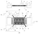
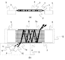
- FIG. 1 shows the configuration of a planar waveguide laser amplifying apparatus according to Embodiment 1 of the present invention.
- FIG. 1A is a side view of a planar waveguide laser amplifying device viewed from the side
- FIG. 1B is a front view of the planar waveguide laser amplifying device viewed from above.
- 1 is a core layer
- 2 is a cladding layer
- 3 is excitation light
- 4 is a planar waveguide
- 5 is a semiconductor laser for excitation
- 6 is a total reflection film
- 7a and 7b are antireflection films
- 8 is a first reflection film.
- 9 is a second signal light laser
- 10 is a first signal light
- 11 is a second signal light
- 12 is a laser amplifier
- 13 is an input unit.
- the same numerals indicate the same or corresponding parts.
- the material of the core layer 1 in the planar waveguide 4 is solid, and a general laser medium can be used.
- a material that absorbs the excitation light 3 emitted from the excitation semiconductor laser 5 is used.
- the pumping semiconductor laser 5 is a pumping light source that outputs pumping light 3 and enters the planar waveguide 4.
- Examples of the medium of the core layer 1 include Nd: YAG, Yb: YAG, Er: YAG, Tm: YAG, Ho: YAG, Nd: YLF, Yb: YLF, Er: YLF, Tm: YLF, Ho: YLF, Nd: Glass, Cr: LiSAF, Ti: Sapphire, etc. are used.
- the clad layer 2 is formed on the upper and lower surfaces of the core layer 1, and the clad layer 2 serves to confine the excitation light 3 in the core layer 1.
- the clad material of the clad layer 2 is composed of a medium having a refractive index n 2 (n 1 > n 2 ) lower than the refractive index n 1 of the core layer 1.
- the medium of the cladding layer 2 for example, can be used as SiO 2, Al 2 O 3, MgF 2.
- the laser amplification device includes a laser amplifier 12 and an input unit 13.
- the input unit 13 includes a first signal light laser 8 and a second signal light laser 9, and outputs a first signal light 10 and a second signal light 11 having the same wavelength, respectively.
- a semiconductor laser or a fiber laser can be used for the first signal light laser 8 and the second signal light laser 9, a semiconductor laser or a fiber laser can be used. In this way, the input unit 13 inputs a plurality of lights to the laser amplifier 12 simultaneously, and the inputted plurality of lights are amplified by the planar waveguide 4.
- the laser amplifier 12 includes a planar waveguide 4 and an excitation semiconductor laser 5, and has a total reflection film 6 and antireflection films 7 a and 7 b on two side surfaces of the planar waveguide 4.
- the total reflection film 6 is a medium that reflects the first signal light 10 and the second signal light 11, and is formed on the two side surfaces of the planar waveguide 4 on which the excitation light 3 is incident.
- the antireflection films 7 a and 7 b are media that transmit the first signal light 10 and the second signal light 11, and are applied to a part of the side surface on which the total reflection film 6 is formed.
- the excitation light 3 emitted from the excitation semiconductor laser 5 is incident from the side surface of the planar waveguide 4.
- the excitation light 3 incident on the planar waveguide 4 is totally reflected at the interface with the cladding layer 2 that is the upper and lower surfaces of the core layer 1.
- the excitation light 3 totally reflected at the interface between the core layer 1 and the cladding layer 2 is confined inside the core layer 1 and guided.
- the pumping light 3 confined and guided inside the core layer 1 is absorbed by the core layer 1 to form an inversion distribution and generate laser gain.
- the first signal light 10 is output from the first signal light laser 8 and is input to the planar waveguide 4 from the antireflection film 7 a.
- the first signal light 10 is totally reflected at the interface between the core layer 1 and the cladding layer 2 in the planar waveguide 4.
- the first signal light 10 totally reflected at the interface between the core layer 1 and the clad layer 2 is confined within the core layer 1 and guided.
- the first signal light 10 proceeds in a zigzag manner while being repeatedly reflected between the total reflection films 6 formed on the side surfaces of the planar waveguide 4, and is induced in the planar waveguide 4 by the excitation semiconductor laser 5. Amplified by laser gain.
- the first signal light 10 passes through the antireflection film 7 b formed on the side surface of the planar waveguide 4 and is output to the outside of the planar waveguide 4.
- the second signal light 11 output from the second signal light laser 9 is also input to the planar waveguide 4 from the antireflection film 7a. Similar to the first signal light 10, the second signal light 11 is confined in the core layer 1 and guided, and is transmitted through the antireflection film 7 b and output to the outside of the planar waveguide 4.
- the first signal light 10 and the second signal light 11 which are a plurality of lights generated at the input unit 13 are input to the planar waveguide 4 in the laser amplifier 12 from the same side surface.
- the angle input to the planar waveguide 4 is different. Therefore, the second signal light 11 follows a different path from the first signal light 10 in the planar waveguide 4, and the gain of the portion of the planar waveguide 4 that cannot use the first signal light 10 can be used. .
- the first embodiment of the present invention includes the laser amplifier 12 that amplifies and outputs the input light, and the input unit that simultaneously inputs a plurality of lights to the laser amplifier 12.
- the first signal light 10 and the second signal light 11, which are a plurality of lights are respectively incident on the excitation light 3 that forms an inversion distribution in the core layer 1 by following different paths. It becomes possible to increase the amplification factor of the laser beam. As a result, it is possible to obtain a higher extraction efficiency than the conventional planar waveguide laser amplifier with respect to the constant intensity pumping light 3 and to improve the extraction efficiency of the output amplified light with respect to the input pumping light.
- the output of the signal light is set to be the same, the output per signal light can be lowered and the nonlinear effects such as Brillouin scattering and Raman scattering can be suppressed compared to the conventional technique in which the output is extracted with a single signal light. Can do.
- the input unit 13 inputs the first signal light 10 and the second signal light 11 from the same side surface of the laser amplifier 12, whereas the second embodiment is from a different side surface of the laser amplifier 12.
- a configuration in which a first signal light 10 and a second signal light 11 are input to a laser amplifier 12 is shown.
- FIG. 2 shows the configuration of a planar waveguide laser amplifying apparatus according to Embodiment 2 of the present invention.
- 2A is a side view of the planar waveguide laser amplifier as viewed from the side
- FIG. 2B is a front view of the planar waveguide laser amplifier as viewed from above.
- 7c and 7d represent antireflection films
- 14 and 15 represent input units.
- the first signal light 10 in the input unit 14 is input to the planar waveguide 4 in the laser amplifier 12 from the antireflection film 7 a on one side of the laser amplifier 12.
- the second signal light 11 in the input unit 15 is input to the planar waveguide 4 of the laser amplifier 12 from the antireflection film 7 c on the other side of the laser amplifier 12.
- the first signal light 10 input from the antireflection film 7 a in the planar waveguide 4 is totally reflected at the interface between the core layer 1 and the cladding layer 2.
- the first signal light 10 totally reflected at the interface between the core layer 1 and the clad layer 2 is confined within the core layer 1 and guided.
- the first signal light 10 proceeds in a zigzag manner while repeating reflection between the total reflection films 6 formed on the side surfaces of the planar waveguide 4 in the direction perpendicular to the waveguide direction, and enters the planar waveguide 4. Amplified by the laser gain induced by the pumping semiconductor laser 5. The first signal light 10 passes through the antireflection film 7 b formed on the side surface of the planar waveguide 4 and is output to the outside of the planar waveguide 4.
- the second signal light 11 input from the antireflection film 7 c provided on the side surface of the laser amplifier 12 opposite to the antireflection film 7 a is confined inside the core layer 1 within the planar waveguide 4. Waveguided.
- the second signal light 11 proceeds in a zigzag manner while being repeatedly reflected between the total reflection films 6 formed on the side surfaces of the planar waveguide 4, and is induced in the planar waveguide 4 by the excitation semiconductor laser 5. Amplified by laser gain.
- the second signal light 11 follows a different path from the first signal light 10 in the planar waveguide 4.
- the second signal light 11 passes through the antireflection film 7 d formed on the side surface of the planar waveguide 4 and is output to the outside of the planar waveguide 4.
- the input units 14 and 15 are characterized by inputting a plurality of lights to different side surfaces of the laser amplifier 12.
- the second signal light 11 follows a path different from that of the first signal light 10 in the planar waveguide 4, and the gain of the portion of the planar waveguide 4 where the first signal light 10 cannot be used can be used.
- the input and output of the first signal light 10 and the second signal light 11 are at the same position, but in the second embodiment, the input and output of the first signal light 10 and the second signal light 11 are performed.
- the position is different.
- the input units 14 and 15 input the first signal light 10 and the second signal light 11 to the laser amplifier 12 from different sides of the laser amplifier 12, respectively.
- the laser power density in the antireflection film 7a is lower than that in the first embodiment, and the possibility of deterioration of the antireflection film 7b due to laser output can be reduced.
- the first signal light 10 and the second signal light 11 are emitted from the individual signal light lasers, whereas in the third embodiment, the first signal light 10 and the second signal light 11 are emitted.
- the signal light 11 is emitted from the same signal light laser.
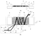
- FIG. 3 shows the configuration of a planar waveguide laser amplifying apparatus according to Embodiment 3 of the present invention.
- 3A is a side view of the planar waveguide laser amplifier as viewed from the side
- FIG. 3B is a front view of the planar waveguide laser amplifier as viewed from above.
- 16 and 17 are total reflection mirrors
- 18 is a beam splitter
- 20 is a laser for signal light.
- the third embodiment is characterized in that the signal light output from the individual signal light lasers in the first and second embodiments is output by a single signal light laser 20.
- the signal light output from the single signal light laser 20 in the input unit 13 is split into the first signal light 10 and the second signal light 11 by the beam splitter 18.
- the angle of the first signal light 10 is adjusted by the total reflection mirror 16 and input to the planar waveguide 4 from the antireflection film 7a.
- the angle of the second signal light 11 is also adjusted by the total reflection mirror 17, and is input to the planar waveguide 4 from the antireflection film 7a.
- a plurality of lights are generated by dividing the light output from the single signal light laser 20 by a splitter such as the beam splitter 18, and the plurality of lights are guided in a plane within the laser amplifier 12 from different positions. Input to the waveguide 4.
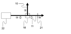
- FIG. 4 is a diagram for explaining a method of dividing the signal light output from the single signal light laser 20 into the first signal light 10 and the second signal light 11.
- a non-polarized laser 22 is used as the signal light laser 20.
- 21 is a half-wave plate
- 22 is a non-polarized laser.
- polarized light perpendicular to the paper surface of FIG. When a laser mixed with polarized light output from the non-polarized laser 22 is input to the polarization beam splitter 18, the polarization component perpendicular to the paper surface is reflected by the polarization beam splitter 18 and becomes the first signal light 10.
- the polarization component parallel to the paper surface is transmitted by the polarization beam splitter 18 and becomes the second signal light 11.
- the polarization beam splitter 18 can separate the light into a plurality of lights. If the half-wave plate 21 is inserted into the first signal light 10 or the second signal light 11, the polarization directions of the first signal 10 and the second signal 11 can be aligned in the same direction. According to the method described in FIG. 4, the first signal light 10 and the second signal light 11 can be obtained from a single laser, and the wavelengths of the first signal light 10 and the second signal light 11 can be obtained. The beam quality can be the same. In this way, the input unit 13 aligns the polarization directions of the plurality of lights by inserting one of the plurality of lights divided by the splitter such as the polarization beam splitter 18 into the half-wave plate.
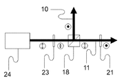
- FIG. 5 is a diagram for explaining another method of dividing the signal light output from the single signal light laser 20 into the first signal light 10 and the second signal light 11.
- reference numeral 23 denotes a half-wave plate
- 24 denotes a linearly polarized laser.
- a linearly polarized laser 24 is used as the signal light laser 20. It is assumed that the linearly polarized laser 24 is polarized parallel to the paper surface of FIG. The polarized light of the laser polarized parallel to the paper surface is rotated 45 degrees by the half-wave plate 23.
- the polarization component perpendicular to the paper surface is reflected by the polarization beam splitter 18 to become the first signal light 10, and the polarization component parallel to the paper surface is the polarization beam splitter 18. And is transmitted as second signal light 11.
- the first signal light 10 and the second signal light 11 can be separated. If the half-wave plate 21 is inserted into the first signal light 10 or the second signal light 11, the polarization directions of the first signal light 10 and the second signal light 11 can be made the same. According to the method described with reference to FIG.
- the first signal light 10 and the second signal light 11 can be obtained from a single laser, and the wavelengths of the first signal light 10 and the second signal light 11 can be obtained.
- the beam quality can be the same.
- the rotation angle of the polarization of the laser is adjusted by the half-wave plate 23 placed in front of the polarization beam splitter 18. By adjusting the rotation angle of the polarization of the laser, the power ratio of the first signal light 10 and the second signal light 11 can be arbitrarily adjusted.
- FIG. 6 is a diagram for explaining another method of dividing the signal light output from the single signal light laser into the first signal light 10 and the second signal light 11.
- reference numeral 25 denotes a partial reflecting mirror.
- the signal light laser 20 may be either a non-polarized laser 22 or a linearly polarized laser 24.
- the output from the signal light laser 20 can be separated into the first signal light 10 and the second signal light 11 by transmission and reflection of the partial reflection mirror 25.
- the first signal light 10 and the second signal light 11 can be obtained from a single laser, and the wavelengths of the first signal light 10 and the second signal light 11 can be obtained.
- the beam quality etc. can be made the same.
- the reflectance of the partial reflection mirror 25 the power ratio of the first signal light 10 and the second signal light 11 can be arbitrarily adjusted.
- the input unit 13 inputs a plurality of lights from different angles of the laser amplifier 12. With such a configuration, it is possible to obtain a higher extraction efficiency than the conventional planar waveguide laser amplifier. Further, the signal light output from the single signal light laser 20 is divided by a splitter such as the polarization beam splitter 18 to generate a plurality of lights. With such a configuration, a plurality of lights can be generated by the single signal light laser 20, and a plurality of lights can be generated efficiently. Further, the input unit 13 inserts one of the plurality of lights divided by the splitter into the half-wave plate. With this configuration, it is possible to align the polarization directions of a plurality of lights.
- the first signal light 10 and the second signal light 11 have the same wavelength, whereas in the fourth embodiment, the first signal light 10 is a plurality of lights. And a configuration in which the second signal light 11 has different wavelengths.
- FIG. 7 shows the configuration of a planar waveguide laser amplifying apparatus according to Embodiment 4 of the present invention.
- FIG. 7A is a side view of the planar waveguide laser amplifying apparatus viewed from the side
- FIG. 7B is a front view of the planar waveguide laser amplifying apparatus viewed from above.
- the second signal light 11 output from the second signal light laser 9 has a wavelength different from that of the first signal light 10 output from the first signal light laser 8.
- the first signal light 10 output from the first signal light laser 8 and the second signal light 11 output from the second signal light laser 9 are input to the planar waveguide 4 from the antireflection film 7a. Is done.
- the first signal light 10 and the second signal light 11 are confined in the core layer 1 and guided.
- the second signal light 11 output from the second signal light laser 9 has a wavelength different from that of the first signal light 10 output from the first signal light laser 8. Accordingly, a plurality of wavelengths can be output from one planar waveguide laser amplifier. Further, if the laser gain has a non-uniform spread, a plurality of signal lights having different wavelengths have different amplification factors. In this case, gain reduction due to spectral hole burning in which a hole is generated in a spectrum of a specific frequency is reduced, and extraction efficiency can be improved.
- the signal light output from the single signal light laser 20 is divided by a splitter such as the polarization beam splitter 18 to generate a plurality of lights.
- a splitter such as the polarization beam splitter 18
- the input unit 13 inserts one of the plurality of lights divided by the splitter into the half-wave plate.
- the clad layer 2 is provided on the upper and lower surfaces of the core layer 1, and the excitation light and the signal light are totally reflected at the interface between the core layer 1 and the clad layer 2 so as to be confined in the core layer 1.
- a second cladding layer having a refractive index lower than that of the cladding layer 2 can be further provided on the upper and lower surfaces of the cladding layer 2.
- the excitation light 3 is totally reflected at the interface between the cladding layer 2 and the second cladding layer and confined inside the core layer 1 and the cladding layer 2.
- the signal light is totally reflected at the interface between the core layer 1 and the clad layer 2 and confined in the core layer 1. Even in such a waveguide having a double clad structure, the method described in the first to fourth embodiments can be performed.
- the input unit 13 inputs a plurality of lights having different wavelengths to the laser amplifier 12. With such a configuration, it is possible to obtain a higher extraction efficiency than the conventional planar waveguide laser amplifier.
- the present invention can be freely combined with each embodiment, or any component of each embodiment can be modified or omitted.
- the number of signal light lasers may be three or more.
- the laser amplifier 12 may be a planar waveguide type laser amplifier.
- a specific configuration in which a plurality of signal lights having different polarizations have different wavelengths is not described.
- an effective configuration in this case will be described.
- a laser medium having the maximum gain at different wavelengths depending on the polarization direction a plurality of signal lights having different wavelengths are input to the planar waveguide laser amplifier in the direction of the polarization direction in which each gain is maximum, A mode of obtaining the maximum amplification gain with each signal light will be described.
- FIG. 8 shows the configuration of a planar waveguide laser amplifying apparatus according to Embodiment 5 of the present invention.
- FIG. 8A is a side view of the planar waveguide laser amplifying device viewed from the side
- FIG. 8B is a front view of the planar waveguide laser amplifying device viewed from above.
- the first signal light 10 output from the first signal light laser 8 and the second signal light 11 output from the second signal light laser 9 have different wavelengths. Furthermore, the polarization directions are perpendicular to each other.
- the core layer 1 is formed of a laser medium having a maximum gain at different wavelengths depending on the polarization direction of the laser light. Examples of the laser medium having the maximum gain at different wavelengths depending on the polarization direction of the laser light include Nd: YLF.
- the signal light has a high gain at a wavelength of 1047 nm for P-polarized light (direction perpendicular to the c-axis of the crystal) and a high gain at a wavelength of 1053 nm for S-polarized light (direction parallel to the c-axis of the crystal).
- the first signal light 10 has a wavelength of 1053 nm and enters the planar waveguide 4 in the laser amplifier 12 from the antireflection film 7a on one side of the laser amplifier 12 so as to be P-polarized with respect to the core layer 1.
- the second signal light 11 in the input unit 15 has a wavelength of 1047 nm and is a laser amplifier from the antireflection film 7 c on the other side of the laser amplifier 12 so as to be S-polarized with respect to the core layer 1.
- 12 plane waveguides 4 are input.
- the c-axis of the crystal of the core layer 1 is a direction parallel to the thickness direction of the waveguide (the c-axis of the crystal of the core layer 1 is perpendicular to the cladding layer 2).
- the first signal light 10 input to the planar waveguide 4 is totally reflected at the interface between the core layer 1 and the clad layer 2 in the planar waveguide 4 and is confined in the core layer 1 and guided. .
- the first signal light 10 proceeds in a zigzag manner while being repeatedly reflected between the total reflection films 6 formed on the side surfaces of the planar waveguide 4, and is induced in the planar waveguide 4 by the excitation semiconductor laser 5. Amplified by laser gain.
- the first signal light 10 passes through the antireflection film 7 b formed on the side surface of the planar waveguide 4 and is output to the outside of the planar waveguide 4.
- the second signal light 11 input from the antireflection film 7 c provided on the side surface of the laser amplifier 12 opposite to the antireflection film 7 a is confined inside the core layer 1 within the planar waveguide 4. Waveguided.
- the second signal light 11 proceeds in a zigzag manner while being repeatedly reflected between the total reflection films 6 formed on the side surfaces of the planar waveguide 4, and is induced in the planar waveguide 4 by the excitation semiconductor laser 5.
- the signal light having a wavelength of 1047 nm is amplified by the laser gain.
- the second signal light 11 follows a different path from the first signal light 10 in the planar waveguide 4.
- the second signal light 11 output from the second signal light laser 9 is the first signal output from the first signal light laser 8. It has a wavelength different from that of the light 10. Since the wavelength 1053 nm of the signal light 10 and the wavelength 1047 nm of the signal light 11 use the same transition band of the laser gain, when the signal light 10 and the signal light 11 pass through the same path in the planar waveguide 4, a larger gain is obtained. The output of the signal light 11 having a wavelength of 1047 nm is larger than that of the signal light 10 having a small gain of 1053 nm.
- the signal light 10 and the signal light 11 follow different paths in the planar waveguide 4, and
- the signal light 10 of 1 can use the gain of the planar waveguide 4 in a portion not used by the second signal light 11.
- signal light of different wavelengths can be obtained with high output from one planar waveguide laser amplifier.
- the clad layer 2 is provided on the upper and lower surfaces of the core layer 1, and the excitation light and the signal light are totally reflected at the interface between the core layer 1 and the clad layer 2 so as to be confined in the core layer 1.
- a second cladding layer having a refractive index lower than that of the cladding layer 2 can be further provided on the upper and lower surfaces of the cladding layer 2.
- the excitation light 3 is totally reflected at the interface between the cladding layer 2 and the second cladding layer and confined inside the core layer 1 and the cladding layer 2.
- the signal light is totally reflected at the interface between the core layer 1 and the clad layer 2 and confined in the core layer 1.
- the method described in the fifth embodiment can be carried out even with such a double clad waveguide.
- the present invention can be freely combined with the fifth embodiment and the first to fourth embodiments, or can be modified or omitted in any component of each embodiment.
- the number of signal light lasers may be three or more.
- the laser amplifier 12 may be a laser amplifier using a slab type laser medium.
- 1 Core layer
- 2 Cladding layer
- 3 Excitation light
- 4 Planar waveguide
- 5 Excitation semiconductor laser
- 6 Total reflection film
- 7a, 7b Antireflection film
- 8 For first signal light
- 10 first signal light
- 11 second signal light
- 12 laser amplifier
- 13 input unit
- 16, 17 total reflection mirror
- 18 polarized beam Splitter
- 20 laser for signal light
- 22 non-polarized laser
- 23 half-wave plate
- 24 linearly polarized laser
- 25 partial reflection mirror
- 26 polarization direction of first signal light
- 27 Polarization direction of the second signal light.
Landscapes
- Physics & Mathematics (AREA)
- Electromagnetism (AREA)
- Engineering & Computer Science (AREA)
- Plasma & Fusion (AREA)
- Optics & Photonics (AREA)
- Lasers (AREA)
Abstract
Description
Claims (9)
- 入力された光を増幅して出力する平面導波路型レーザ増幅器と、
前記平面導波路型レーザ増幅器に複数の光を同時に入力する入力部と、
を備えたことを特徴とするレーザ増幅装置。 - 前記入力部は前記複数の光を前記平面導波路型レーザ増幅器の異なる角度または異なる側面から入力することを特徴とする請求項1に記載のレーザ増幅装置。
- 前記入力部は単一の信号光用レーザから出力された光をスプリッタで分割することで前記複数の光を生成することを特徴とする請求項1または請求項2に記載のレーザ増幅装置。
- 前記入力部はスプリッタで分割された前記複数の光の一方が挿入される半波長板を設けたことを特徴とする請求項3に記載のレーザ増幅装置。
- 前記複数の光は異なる波長を有することを特徴とする請求項1または請求項2に記載のレーザ増幅装置。
- 前記平面導波路型レーザ増幅器は平板状レーザ媒質と前記平板状レーザ媒質の上下面に形成されたクラッドとを含み、前記複数の光は前記上下面に形成されたクラッドで全反射され前記平板状レーザ媒質内に閉じ込められることを特徴とする請求項1に記載のレーザ増幅装置。
- 前記複数の光は前記平面状レーザ媒質内で異なる経路をたどることを特徴とする請求項6に記載のレーザ増幅装置。
- 前記平板状レーザ媒質は光によって励起され、
前記平面導波路型レーザ増幅器内の平面導波路は前記光が入力される側面に反射膜及び反射防止膜を備えた
ことを特徴とする請求項7に記載のレーザ増幅装置。 - 前記複数の光は互いに直交する偏光方向を有する異なる波長の光であり、
前記平面導波路型レーザ増幅器に含まれるレーザ媒質は前記入力された光の偏光方向により異なる波長に最大の利得を有することを特徴とする請求項1、2、6乃至8のいずれか1項に記載のレーザ増幅装置。
Priority Applications (4)
| Application Number | Priority Date | Filing Date | Title |
|---|---|---|---|
| EP14840437.9A EP3043429A4 (en) | 2013-09-02 | 2014-05-14 | Laser amplification device |
| JP2015533939A JPWO2015029285A1 (ja) | 2013-09-02 | 2014-05-14 | レーザ増幅装置 |
| CN201480048329.3A CN105531888A (zh) | 2013-09-02 | 2014-05-14 | 激光放大装置 |
| US14/915,741 US9698556B2 (en) | 2013-09-02 | 2014-05-14 | Laser amplification device |
Applications Claiming Priority (2)
| Application Number | Priority Date | Filing Date | Title |
|---|---|---|---|
| JP2013-180874 | 2013-09-02 | ||
| JP2013180874 | 2013-09-02 |
Publications (1)
| Publication Number | Publication Date |
|---|---|
| WO2015029285A1 true WO2015029285A1 (ja) | 2015-03-05 |
Family
ID=52585885
Family Applications (1)
| Application Number | Title | Priority Date | Filing Date |
|---|---|---|---|
| PCT/JP2014/002542 Ceased WO2015029285A1 (ja) | 2013-09-02 | 2014-05-14 | レーザ増幅装置 |
Country Status (5)
| Country | Link |
|---|---|
| US (1) | US9698556B2 (ja) |
| EP (1) | EP3043429A4 (ja) |
| JP (1) | JPWO2015029285A1 (ja) |
| CN (1) | CN105531888A (ja) |
| WO (1) | WO2015029285A1 (ja) |
Cited By (1)
| Publication number | Priority date | Publication date | Assignee | Title |
|---|---|---|---|---|
| JP2023544714A (ja) * | 2020-09-30 | 2023-10-25 | 華為技術有限公司 | 光学ファイバ増幅装置 |
Families Citing this family (2)
| Publication number | Priority date | Publication date | Assignee | Title |
|---|---|---|---|---|
| KR102626918B1 (ko) | 2017-02-02 | 2024-01-18 | 삼성전자주식회사 | 증폭 도파 장치 및 이를 포함한 증폭 빔 스티어링 장치 |
| JP6811898B1 (ja) * | 2019-12-18 | 2021-01-13 | 三菱電機株式会社 | 平面導波路型増幅器およびレーザレーダ装置 |
Citations (12)
| Publication number | Priority date | Publication date | Assignee | Title |
|---|---|---|---|---|
| JPS62200781A (ja) * | 1986-02-28 | 1987-09-04 | Toshiba Corp | レ−ザ装置 |
| JPH02260678A (ja) * | 1989-03-31 | 1990-10-23 | Hoya Corp | レーザ装置 |
| US5268787A (en) * | 1993-02-17 | 1993-12-07 | Energy Compression Research Corp. | Multiple-pass method and apparatus for laser amplification |
| US6061377A (en) * | 1996-12-04 | 2000-05-09 | Thomson-Csf | Light amplifier device with two incident beams |
| JP2003023194A (ja) * | 2001-07-05 | 2003-01-24 | Japan Atom Energy Res Inst | 固体レーザー増幅器 |
| US20030063884A1 (en) | 2001-01-04 | 2003-04-03 | Smith Duane D. | Power scalable optical systems for generating, transporting, and delivering high power, high quality, laser beams |
| JP2007227448A (ja) * | 2006-02-21 | 2007-09-06 | Mitsubishi Electric Corp | 再生増幅器、モードロックレーザ及び利得平滑化方法 |
| JP2008522409A (ja) * | 2004-11-26 | 2008-06-26 | ジェフリー, ジー マンニ, | 高利得ダイオード励起レーザ増幅器 |
| JP2009277943A (ja) * | 2008-05-15 | 2009-11-26 | Mitsubishi Electric Corp | 光増幅器及び光発振器 |
| JP2011517066A (ja) * | 2008-03-31 | 2011-05-26 | エレクトロ サイエンティフィック インダストリーズ インコーポレーテッド | マルチパス光パワー増幅器 |
| JP2011129826A (ja) * | 2009-12-21 | 2011-06-30 | Mitsubishi Electric Corp | 固体レーザ装置 |
| JP2012078813A (ja) * | 2010-09-06 | 2012-04-19 | Osaka Univ | レーザ装置 |
Family Cites Families (7)
| Publication number | Priority date | Publication date | Assignee | Title |
|---|---|---|---|---|
| US6330088B1 (en) * | 1998-02-27 | 2001-12-11 | Zebra Imaging, Inc. | Method and apparatus for recording one-step, full-color, full-parallax, holographic stereograms |
| US6483859B1 (en) | 1999-06-24 | 2002-11-19 | Lockheed Martin Corporation | System and method for high-speed laser detection of ultrasound |
| JP2005251981A (ja) | 2004-03-04 | 2005-09-15 | Japan Atom Energy Res Inst | 固体レーザーの増幅法 |
| US7280571B2 (en) | 2004-11-23 | 2007-10-09 | Northrop Grumman Corporation | Scalable zig-zag laser amplifier |
| CN101877455B (zh) * | 2009-04-28 | 2013-02-06 | 高质激光有限公司 | 激光放大装置和激光放大方法 |
| US8149886B2 (en) | 2009-04-28 | 2012-04-03 | High Q Technologies Gmbh | Laser amplifier system and laser amplifier method |
| KR20140006782A (ko) | 2010-09-06 | 2014-01-16 | 오사카 유니버시티 | 레이저장치 |
-
2014
- 2014-05-14 US US14/915,741 patent/US9698556B2/en active Active
- 2014-05-14 CN CN201480048329.3A patent/CN105531888A/zh active Pending
- 2014-05-14 JP JP2015533939A patent/JPWO2015029285A1/ja active Pending
- 2014-05-14 EP EP14840437.9A patent/EP3043429A4/en not_active Withdrawn
- 2014-05-14 WO PCT/JP2014/002542 patent/WO2015029285A1/ja not_active Ceased
Patent Citations (12)
| Publication number | Priority date | Publication date | Assignee | Title |
|---|---|---|---|---|
| JPS62200781A (ja) * | 1986-02-28 | 1987-09-04 | Toshiba Corp | レ−ザ装置 |
| JPH02260678A (ja) * | 1989-03-31 | 1990-10-23 | Hoya Corp | レーザ装置 |
| US5268787A (en) * | 1993-02-17 | 1993-12-07 | Energy Compression Research Corp. | Multiple-pass method and apparatus for laser amplification |
| US6061377A (en) * | 1996-12-04 | 2000-05-09 | Thomson-Csf | Light amplifier device with two incident beams |
| US20030063884A1 (en) | 2001-01-04 | 2003-04-03 | Smith Duane D. | Power scalable optical systems for generating, transporting, and delivering high power, high quality, laser beams |
| JP2003023194A (ja) * | 2001-07-05 | 2003-01-24 | Japan Atom Energy Res Inst | 固体レーザー増幅器 |
| JP2008522409A (ja) * | 2004-11-26 | 2008-06-26 | ジェフリー, ジー マンニ, | 高利得ダイオード励起レーザ増幅器 |
| JP2007227448A (ja) * | 2006-02-21 | 2007-09-06 | Mitsubishi Electric Corp | 再生増幅器、モードロックレーザ及び利得平滑化方法 |
| JP2011517066A (ja) * | 2008-03-31 | 2011-05-26 | エレクトロ サイエンティフィック インダストリーズ インコーポレーテッド | マルチパス光パワー増幅器 |
| JP2009277943A (ja) * | 2008-05-15 | 2009-11-26 | Mitsubishi Electric Corp | 光増幅器及び光発振器 |
| JP2011129826A (ja) * | 2009-12-21 | 2011-06-30 | Mitsubishi Electric Corp | 固体レーザ装置 |
| JP2012078813A (ja) * | 2010-09-06 | 2012-04-19 | Osaka Univ | レーザ装置 |
Non-Patent Citations (1)
| Title |
|---|
| See also references of EP3043429A4 * |
Cited By (2)
| Publication number | Priority date | Publication date | Assignee | Title |
|---|---|---|---|---|
| JP2023544714A (ja) * | 2020-09-30 | 2023-10-25 | 華為技術有限公司 | 光学ファイバ増幅装置 |
| JP7490892B2 (ja) | 2020-09-30 | 2024-05-27 | 華為技術有限公司 | 光学ファイバ増幅装置 |
Also Published As
| Publication number | Publication date |
|---|---|
| JPWO2015029285A1 (ja) | 2017-03-02 |
| EP3043429A4 (en) | 2017-05-03 |
| US9698556B2 (en) | 2017-07-04 |
| CN105531888A (zh) | 2016-04-27 |
| EP3043429A1 (en) | 2016-07-13 |
| US20160197450A1 (en) | 2016-07-07 |
Similar Documents
| Publication | Publication Date | Title |
|---|---|---|
| JP4226482B2 (ja) | レーザ光合波装置 | |
| JP4754020B2 (ja) | 平面導波路型レーザ装置 | |
| JP3588195B2 (ja) | 固体レーザ増幅器 | |
| US6667999B2 (en) | Cooling of high power laser systems | |
| JP6253672B2 (ja) | 平面導波路型レーザ装置 | |
| Bae et al. | Controllable Dynamic Single‐and Dual‐Channel Graphene Q‐Switching in a Beam‐Splitter‐Type Channel Waveguide Laser | |
| US20220294170A1 (en) | Planar waveguide amplifier and laser radar device | |
| JPWO2009028078A1 (ja) | 固体レーザ素子 | |
| JPWO2015029285A1 (ja) | レーザ増幅装置 | |
| JP5645753B2 (ja) | 平面導波路型レーザ装置 | |
| JP2012160645A (ja) | 固体レーザ装置 | |
| WO2011027579A1 (ja) | 平面導波路型レーザ装置 | |
| JP6437169B2 (ja) | リッジ導波路型レーザ装置 | |
| JP2008098496A (ja) | チャープパルス増幅器及び増幅方法 | |
| CN111512504B (zh) | 平面波导和激光放大器 | |
| JP2011254035A (ja) | 固体レーザ装置 | |
| JP5987193B2 (ja) | 光増幅器 | |
| JP2011129826A (ja) | 固体レーザ装置 | |
| JPH08125257A (ja) | 光増幅装置 | |
| JP2009182053A (ja) | レーザー装置 | |
| CN118589284A (zh) | 一种相干倍频合束飞秒光纤激光器 | |
| JP2014167989A (ja) | ロッド型ファイバレーザ増幅器 | |
| WO2002021192A1 (fr) | Multiplexeur optique polarise | |
| JPH10200184A (ja) | 固体レーザ装置 | |
| JP2013219137A (ja) | 平面導波路型レーザ装置 |
Legal Events
| Date | Code | Title | Description |
|---|---|---|---|
| WWE | Wipo information: entry into national phase |
Ref document number: 201480048329.3 Country of ref document: CN |
|
| 121 | Ep: the epo has been informed by wipo that ep was designated in this application |
Ref document number: 14840437 Country of ref document: EP Kind code of ref document: A1 |
|
| REEP | Request for entry into the european phase |
Ref document number: 2014840437 Country of ref document: EP |
|
| WWE | Wipo information: entry into national phase |
Ref document number: 2014840437 Country of ref document: EP |
|
| ENP | Entry into the national phase |
Ref document number: 2015533939 Country of ref document: JP Kind code of ref document: A |
|
| WWE | Wipo information: entry into national phase |
Ref document number: 14915741 Country of ref document: US |
|
| NENP | Non-entry into the national phase |
Ref country code: DE |