WO2015043524A1 - 自干扰信号消除设备及方法 - Google Patents
自干扰信号消除设备及方法 Download PDFInfo
- Publication number
- WO2015043524A1 WO2015043524A1 PCT/CN2014/087679 CN2014087679W WO2015043524A1 WO 2015043524 A1 WO2015043524 A1 WO 2015043524A1 CN 2014087679 W CN2014087679 W CN 2014087679W WO 2015043524 A1 WO2015043524 A1 WO 2015043524A1
- Authority
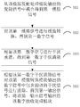
- WO
- WIPO (PCT)
- Prior art keywords
- signal
- digital
- analog
- module
- interference
- Prior art date
- Legal status (The legal status is an assumption and is not a legal conclusion. Google has not performed a legal analysis and makes no representation as to the accuracy of the status listed.)
- Ceased
Links
Images


Classifications
-
- H—ELECTRICITY
- H04—ELECTRIC COMMUNICATION TECHNIQUE
- H04B—TRANSMISSION
- H04B15/00—Suppression or limitation of noise or interference
-
- H—ELECTRICITY
- H04—ELECTRIC COMMUNICATION TECHNIQUE
- H04B—TRANSMISSION
- H04B1/00—Details of transmission systems, not covered by a single one of groups H04B3/00 - H04B13/00; Details of transmission systems not characterised by the medium used for transmission
- H04B1/06—Receivers
- H04B1/10—Means associated with receiver for limiting or suppressing noise or interference
- H04B1/12—Neutralising, balancing, or compensation arrangements
- H04B1/123—Neutralising, balancing, or compensation arrangements using adaptive balancing or compensation means
-
- H—ELECTRICITY
- H04—ELECTRIC COMMUNICATION TECHNIQUE
- H04B—TRANSMISSION
- H04B1/00—Details of transmission systems, not covered by a single one of groups H04B3/00 - H04B13/00; Details of transmission systems not characterised by the medium used for transmission
- H04B1/38—Transceivers, i.e. devices in which transmitter and receiver form a structural unit and in which at least one part is used for functions of transmitting and receiving
- H04B1/40—Circuits
- H04B1/50—Circuits using different frequencies for the two directions of communication
- H04B1/52—Hybrid arrangements, i.e. arrangements for transition from single-path two-direction transmission to single-direction transmission on each of two paths or vice versa
- H04B1/525—Hybrid arrangements, i.e. arrangements for transition from single-path two-direction transmission to single-direction transmission on each of two paths or vice versa with means for reducing leakage of transmitter signal into the receiver
Definitions
- Full-duplex wireless communication technology is a technology different from TDD and FDD. With this technology, simultaneous communication at the same frequency can be realized. However, when two communication devices communicate at the same frequency, the receiving antenna not only receives the useful signal from the opposite end, but also receives the signal transmitted by itself, which is the self-interference signal. And because the distance between the transmitting antenna and the receiving antenna is relatively close, the strength of the self-interference signal is often much higher than the useful signal at the opposite end.
- a self-interference signal cancellation device comprising: a digital transmission processing module, an analog transmission processing module, a first analog to digital conversion module, an analog receiving processing module, and a digital receiving processing module, the analog transmitting processing
- the transmitting signal outputted by the module is transmitted to the first analog-to-digital conversion module via an air interface to form a self-interference signal
- the digital signal output by the first analog-to-digital conversion module includes the self-interference signal
- the device further includes a first Self-interference cancellation unit
- the first signal coupling module is configured to couple a first analog signal from a transmit signal output by the analog transmit processing module, and output the first analog signal to the first analog feedback processing module;
- the second analog-to-digital conversion module is configured to perform analog-to-digital conversion on the first analog signal to obtain a first digital signal, and output the first digital signal to the first digital interference reconstruction module;
- the first digital interference cancellation module is configured to cancel the self-interference signal included in the digital signal output by the first analog-to-digital conversion module according to the first digital interference cancellation signal, to obtain a first output signal, and The first output signal is output to the digital receive processing module.
- the device further includes: a second self-interference cancellation unit;
- the resulting signal is eliminated from being output to the analog receive processing module.
- the second self-interference cancellation unit includes: a second digital interference reconstruction module, a second digital-to-analog conversion module, and a first signal synthesis module,
- the second digital interference reconstruction module is configured to perform interference reconstruction according to the digital transmission signal output by the digital transmission processing module, to obtain a second digital interference cancellation signal, and output the second digital interference cancellation signal to the second number Mode conversion module
- the second digital-to-analog conversion module is configured to perform digital-to-analog conversion on the second digital interference cancellation signal to obtain a first analog composite signal, and output the first analog composite signal to the first signal synthesis module;
- the first signal synthesis module is configured to cancel a self-interference signal in the analog received signal received by the receiving antenna according to the first analog composite signal, to eliminate linearity of the self-interference signal in the analog received signal section.
- the device further includes: a third self-interference cancellation unit;
- the third self-interference cancellation unit is configured to couple the third analog signal from the first analog composite signal
- the third self-interference cancellation unit includes: a second signal coupling module, a third analog-to-digital conversion module, and a third digital interference reconstruction module,
- the second signal coupling module is configured to couple a third analog signal from the first analog composite signal, and output the third analog signal to the third analog to digital conversion module;
- the third analog-to-digital conversion module is configured to perform analog-to-digital conversion on the third analog signal to obtain a third digital signal, and output the third digital signal to the third digital interference reconstruction module;
- the third digital interference reconstruction module is configured to perform interference reconstruction according to the third digital signal to obtain a third digital interference cancellation signal, and output the third digital interference cancellation signal to the first digital interference cancellation module;
- the first digital interference cancellation module is further configured to: cancel the self-interference signal in the first output signal according to the third digital interference cancellation signal, to obtain a second output signal, and output the second output The signal is output to the digital receive processing module.
- the first digital interference reconstruction module is configured to process the first digital signal according to the digital transmission signal output by the digital transmission processing module, and remove the digital transmission signal portion of the first digital signal;
- the first digital signal performs interference reconstruction to obtain a first digital interference cancellation signal, and outputs the first digital interference cancellation signal to the first digital interference cancellation module.
- the third digital interference reconstruction module is configured to perform the third digital signal according to the digital transmit signal output by the digital transmit processing module Processing, removing the digital transmission signal portion of the third digital signal; performing interference reconstruction according to the third digital signal from which the digital transmission signal portion is removed, obtaining a third digital interference cancellation signal, and outputting the third digital interference cancellation signal to The first digital interference cancellation module.
- the second analog-to-digital conversion module includes: a first analog feedback processing sub-module and a second analog-to-digital conversion sub-module,
- the first analog feedback processing sub-module is configured to process the first analog signal output by the first signal coupling module to obtain a second analog signal, and output the second analog signal to the second modulus Conversion submodule;
- the second analog-to-digital conversion sub-module is configured to perform analog-to-digital conversion on the second analog signal output by the first analog feedback processing sub-module to obtain a first digital signal, and output the first digital signal to the The first digital interference reconstruction module.
- the first analog feedback processing submodule includes: a first filter and a first down converter
- the first filter is configured to perform filtering processing on the first analog signal to obtain a first filtered analog signal, and output the first filtered analog signal to the first down converter;
- the first down converter is configured to downconvert the first filtered analog signal to obtain the second analog signal, and output the second analog signal to the second analog to digital conversion submodule.
- the first reconstruction analog processing sub-module is configured to process the second analog interference cancellation signal output by the second digital-to-analog conversion sub-module to obtain a first analog composite signal, and output the first analog composite signal to the
- the first signal synthesis module is described.
- the first re-conversion analog processing sub-module includes: a first up-converter and a first gain amplifier,
- the first up-converter is configured to up-convert the second digital interference cancellation signal to obtain the first up-converted analog signal, and output the first up-converted analog signal to the first gain amplifier;
- the first gain amplifier is configured to perform amplification processing on the first up-converted analog signal to obtain the first analog composite signal, and output the first analog composite signal to the first signal synthesis module.
- the third analog-to-digital conversion module includes: a second analog feedback processing sub-module and a third analog-to-digital conversion sub-module,
- the second analog feedback processing sub-module is configured to process the third analog signal to obtain a fourth analog signal, and output the fourth analog signal to the third analog-to-digital conversion sub-module;
- the third analog-to-digital conversion sub-module is configured to perform analog-to-digital conversion on the third analog signal output by the second analog feedback processing sub-module to obtain a third digital signal, and output the third digital signal to the The third digital interference reconstruction module.
- a self-interference signal cancellation method which is applicable to a communication device, and the device includes: a digital transmission processing module, an analog transmission processing module, a first analog to digital conversion module, an analog receiving processing module, and a digital receiving processing module.
- the transmission signal output by the analog transmission processing module is transmitted to the first analog-to-digital conversion module via an air interface to form a self-interference signal, and the digital signal output by the first analog-to-digital conversion module includes the self-interference signal.
- the methods include:
- the method further includes:
- the resulting signal is eliminated from being output to the analog receive processing module.
- the method further includes:
- the method further includes:
- performing digital-to-analog conversion on the second digital interference cancellation signal, to obtain the first analog composite signal including:
- performing analog-to-digital conversion on the third analog signal, and obtaining the third digital signal includes:
- the device and the method provided by the embodiment of the present invention by adding a first self-interference cancellation unit, coupling a first analog signal from a transmission signal of the analog transmission processing module, and converting the first analog signal into a first digital signal, according to the Performing interference reconstruction on the first digital signal to obtain a first digital interference cancellation signal, and canceling the self-interference signal included in the digital signal output by the first analog-to-digital conversion module according to the first digital interference cancellation signal to obtain a first output signal.
- the first analog signal is obtained by coupling from the transmitted signal
- the first digital interference cancellation signal finally obtained according to the first analog signal includes a linear portion, a nonlinear portion, a noise portion, and the like of the self-interference signal, and thus, After the interference cancellation of the first digital interference cancellation signal and the digital signal output by the first analog-to-digital conversion module, the self-interference signal introduced during the transmission process can be eliminated.
- FIG. 1b is a schematic structural diagram of a self-interference signal canceling apparatus according to an embodiment of the present invention.
- FIG. 2a is a schematic structural diagram of a self-interference signal canceling apparatus according to an embodiment of the present invention
- FIG. 2b A comparison diagram of an embodiment of the present invention and a conventional digital domain coupling cancellation method is shown in FIG. 2b;
- FIG. 3 is a schematic structural diagram of a self-interference signal canceling apparatus according to an embodiment of the present invention.
- FIG. 4 is a schematic structural diagram of a self-interference signal canceling apparatus according to an embodiment of the present invention.
- FIG. 5 is a flowchart of a method for canceling self-interference signals according to an embodiment of the present invention.
- FIG. 1 is a schematic structural diagram of a self-interference signal canceling apparatus according to an embodiment of the present invention.
- the device includes a digital transmission processing module 101, an analog transmission processing module 103, a digital reception processing module 104, a first analog to digital conversion module 105, and an analog reception processing module 106.
- the transmit signal output by the analog transmit processing module 103 is transmitted to the first analog-to-digital conversion module 105 via the air interface to form a self-interference signal.
- the digital signal output by the first analog-to-digital conversion module 105 includes the self-interference signal, and the device further includes: a self-interference cancellation unit 100;
- the first self-interference cancellation unit 100 is configured to couple a first analog signal from a transmit signal output by the analog transmit processing module, and perform analog-to-digital conversion on the first analog signal to obtain a first digital signal. According to the first digital The signal is subjected to interference reconstruction to obtain a first digital interference cancellation signal; and the self-interference signal included in the digital signal output by the first analog-to-digital conversion module is eliminated according to the first digital interference cancellation signal to obtain a first output signal, The first output signal Output to the digital receive processing module.
- the self-interference signal component is represented by only the self-interference signal, and the signal form is defined by the same signal as the signal carrying the component, for example, the “self-interference signal included in the digital signal”. It refers to the self-interference signal component contained in the digital signal.
- the signal form of the self-interference signal is a digital signal.
- the analog transmission processing module at the transmitting end and the analog to digital conversion converts the analog signal to generate a certain distortion (such as the phase noise introduced by the mixing, the nonlinearity introduced by the power amplifier and the noise floor), and these distortions
- the signal is transmitted through the antenna and leaks to the receiving end.
- Direct linear modeling of the digital signal before digital-to-analog conversion cannot reconstruct these effects.
- Even nonlinear modeling cannot reconstruct phase noise and noise floor, so the performance of interference cancellation is eliminated. Not good.
- the first analog signal is coupled from the transmission signal of the analog transmission processing module, and the first analog signal is converted into the first digital signal, according to the first Performing interference reconstruction on a digital signal to obtain a first digital interference cancellation signal, and canceling the self-interference signal included in the digital signal output by the first analog-to-digital conversion module according to the first digital interference cancellation signal to obtain a first output signal .
- the first analog signal is obtained by coupling from the transmitted signal
- the first digital interference cancellation signal finally obtained according to the first analog signal includes a linear portion, a nonlinear portion, a noise portion, and the like of the self-interference signal, and thus, After the interference cancellation of the first digital interference cancellation signal and the digital signal output by the first analog-to-digital conversion module, the self-interference signal introduced during the transmission process can be eliminated.
- FIG. 1b is a schematic structural diagram of a self-interference signal canceling apparatus according to an embodiment of the present invention.
- the device includes: a digital transmit processing module 101, a first digital-to-analog conversion module 102, an analog transmit processing module 103, and a transmit antenna TX1.
- the receive channel includes a digital receive processing module 104 and a first analog-to-digital conversion module 105.
- the first self-interference cancellation unit 100 includes a first signal coupling module 107, a second analog-to-digital conversion module 108, a first digital interference reconstruction module 109, and a first digital interference cancellation module 110.
- the first signal coupling module 107 is configured to obtain a first analog signal from the transmit signal output by the analog transmit processing module 103 of the transmit channel, and output the first analog signal to the second analog to digital conversion module 108;
- the first digital interference reconstruction module 109 is configured to perform interference reconstruction according to the first digital signal, to obtain a first digital interference cancellation signal, and output the first digital interference cancellation signal to the first digital interference cancellation module 110;
- the device by adding a first self-interference cancellation unit, coupling a first analog signal from a transmission signal of the analog transmission processing module, and converting the first analog signal into a first digital signal, according to the first
- the digital signal is subjected to interference reconstruction to obtain a first digital interference cancellation signal, and the self-interference signal included in the digital signal output by the first analog-to-digital conversion module is cancelled according to the first digital interference cancellation signal to obtain a first output signal.
- FIG. 2 is a schematic structural diagram of a self-interference signal canceling apparatus according to an embodiment of the present invention.
- the device can be applied to a commonly used superheterodyne receiver architecture.
- the device includes: a digital transmission processing module 201, a first digital-to-analog conversion module 202, an analog transmission processing module 203, a transmitting antenna TX2, a digital receiving processing module 204, a first analog-to-digital conversion module 205, and an analog receiving processing module. 206.
- Receive antenna RX2 Receive antenna RX2.
- the digital transmission processing module 201 of the transmission channel is generally implemented by using a transmitter, and is configured to generate a digital transmission signal, and output the digital transmission signal to the first digital-to-analog conversion module 202;
- a digital-to-analog conversion module 202 can be implemented by using a digital-to-analog converter for digital-to-analog conversion of the digital transmission signal to obtain an analog transmission signal corresponding to the digital transmission signal, and outputting the analog transmission signal to the analog transmission.
- the processing module 203 is generally implemented by using a frequency converter and a power amplifier for performing frequency conversion and power amplification on the analog transmission information, obtaining a transmission signal, and transmitting the transmission signal through the transmitting antenna TX2. .
- the receiving antenna RX2 is used to receive an analog signal; since the parameters of the analog signal received by the receiving antenna are uncontrollable, the analog receiving processing module 206 can employ a low noise amplifier, a filter, and a frequency conversion.
- the device is configured to perform low noise amplification, filtering, and frequency conversion processing on the analog receiving signal received by the receiving antenna RX2, and output the processed analog signal to the first analog to digital conversion module 205; the first modulus
- the conversion module 205 is generally implemented by an analog-to-digital converter for converting an analog signal after low-noise amplification, filtering, and frequency conversion processing by the analog reception processing module 206 into a digital signal, and is received by the digital reception processing module 204.
- the digital signal is received, and the receive channel digital receive processing module 204 is typically implemented using a receiver.
- the apparatus further includes a first self-interference cancellation unit for canceling a self-interference signal in the received signal
- the self-interference signal may include a linear portion, a nonlinear portion, and a noise portion, the linear portion being The digital transmit signal of the transmit channel is introduced, and the non-linear portion and the noise portion are introduced by the transmit channel.
- the first self-interference cancellation unit includes: a first signal coupling module 207, and a second mode The number conversion module 208, the first digital interference reconstruction module 209, and the first digital interference cancellation module 210.
- each module constituting the first self-interference cancellation unit is introduced:
- a first signal coupling module 207 (1) A first signal coupling module 207.
- the first signal coupling module 207 can be implemented by using a coupler.
- the first analog signal is a part of the analog signal coupled out from the transmit signal output by the first signal coupling module 207 from the analog transmit processing module 203.
- the transmit signal output by the analog transmit processing module 203 can be divided into two parts according to the preset coupling parameters of the first signal coupling module 207, and a part is used for interference reconstruction, and another Part of it is used for output to the transmitting front end for transmission.
- the second analog to digital conversion module 208 includes:
- One end of the second analog-to-digital conversion module 208 is connected to the first signal coupling module 207, and the other end is connected to the first digital interference reconstruction module 209, and the second analog-to-digital conversion module 208 is configured to perform analog-to-digital conversion on the first analog signal. And obtaining a first digital signal, and outputting the first digital signal to the first digital interference reconstruction module 209.
- the second analog-to-digital conversion module 208 includes: a first analog feedback processing sub-module 2081 and a second analog-to-digital conversion sub-module 2082.
- the first analog feedback processing sub-module 2081 is configured to process the first analog signal output by the first signal coupling module 107 to obtain a second analog signal, and output the second analog signal to the second analog-to-digital converter.
- the second analog-to-digital conversion sub-module 2082 is configured to enter the second analog signal output by the first analog feedback processing sub-module 2081.
- the first digital signal is output to the first digital interference reconstruction module 209 by row analog to digital conversion.
- first analog feedback processing sub-module 2081 is connected to the first signal coupling module 207, and the other end is connected to the second analog-to-digital conversion sub-module 2082, and the first analog feedback processing sub-module 2081 is used.
- the first analog signal output by the first signal coupling module 207 is processed to obtain a second analog signal, and the second analog signal is output to the second analog to digital conversion submodule 2082.
- the processing performed by the first analog feedback processing sub-module 2081 includes, but is not limited to, filtering and frequency conversion of analog signals, and the like.
- the first analog feedback processing sub-module 2081 includes a first filter 20811 and a first down converter 20812.
- the first filter 20811 can be implemented by a filter
- the first down converter 20812 can be implemented by using a frequency converter and a local oscillator.
- the first filter 20811 and the first down converter 20812 are respectively introduced below:
- the first down converter 20812 is used for down-converting the first filtered analog signal output by the first filter 20811 to obtain a first down-converted analog signal, and outputting the first down-converted analog signal
- the second analog to digital conversion sub-module 2082 is provided.
- the purpose of the down-conversion is to frequency-convert the local oscillator frequency generated by the local oscillator with the first filtered analog signal to obtain a first down-converted analog signal having a second preset frequency.
- the first analog feedback processing module 2081 further includes: a first low noise amplifier, the low noise amplifier may be located between the first filter 20811 and the first signal coupling module 207, and one end of the low noise amplifier is connected to the first signal coupling module 207.
- the other end is connected to the first filter 20811, and the low noise amplifier is configured to perform low noise amplification on the first analog signal output by the first signal coupling module 207 to obtain a first amplified analog signal, and the first amplified analog signal is obtained.
- the first filter 20811 is output to the first filter 20811, so that the first filter 20811 filters the received signal to obtain a first filtered analog signal, and outputs the first filtered analog signal to the first down converter 20812.
- the first low noise amplifier can be implemented with a low noise amplifier that suppresses interference signals.
- first preset frequency and the second preset frequency are both matched with the actual parameters of the device, and may be adjusted according to the change of the actual parameters of the device, which is not specifically limited in this embodiment of the present invention.
- One end of the second analog-to-digital conversion sub-module 2082 is connected to the first analog feedback processing module 208, and the other end is connected to the first digital interference reconstruction module 209, and the second analog-to-digital conversion sub-module 2082 is used to the first analog feedback.
- the second analog signal output by the processing module 208 performs analog-to-digital conversion to obtain a first digital signal, and outputs the first digital signal to the first digital interference reconstruction module 209.
- the second analog to digital conversion submodule 2082 can be implemented by using an analog to digital converter.
- the first digital interference reconstruction module 209 is connected to the second analog to digital conversion module 208, and the other end is connected to the first digital interference cancellation module 210.
- the first digital interference reconstruction module 209 is configured to perform interference reconstruction according to the first digital signal to obtain a first digital interference cancellation signal, and output the first digital interference cancellation signal to the first digital interference cancellation module 210.
- the first digital interference cancellation signal includes a linear portion, a nonlinear portion, and a noise portion of the self-interference signal.
- the first digital interference reconstruction module 209 is mainly used for transmitting channels.
- the self-interference signal is reconstructed, and the interference reconstruction can be implemented in a training or adaptive manner.
- the interference reconstruction process may obtain the first digital interference cancellation signal by performing amplitude modulation, frequency conversion, and phase modulation processing on the first digital signal, so that the first digital interference cancellation signal and the receiving channel are introduced by the transmitting channel.
- the amplitude and frequency of the interference signal are the same, and the phases are 180 degrees out of phase, so that the first digital interference cancellation signal can be cancelled by the interference signal introduced by the transmission channel in the receiving channel.
- the first digital interference cancellation module 210 The first digital interference cancellation module 210.
- the first digital interference cancellation module 210 includes two inputs and an output.
- the first digital interference cancellation module 210 receives the first digital interference cancellation signal output by the first digital interference reconstruction module 209 and the first analog to digital conversion module 205 in the receiving channel.
- the first digital interference cancellation module 210 is configured to cancel the self-interference signal included in the digital signal output by the first analog-to-digital conversion module according to the first digital interference cancellation signal, to obtain a first output signal, where the first The output signal is output to the digital receive processing module 204.
- the digital transmission signal output by the digital transmission processing module 201 is X[k]
- the digital transmission signal is processed by the first digital-to-analog conversion module 202 and the analog transmission processing module 203, and the nonlinear portion of the self-interference signal is introduced.
- the noise part N[t] the obtained transmission signal is X[t]+N[t]
- the receiving signal of the receiving front end includes the self-interference signal part H[t]*(X[t]+N[t]) and the pre- Receive signal S[t].
- the received signal H[t]*(X[t]+N[t])+S[t] is processed by the analog receiving processing module 206 and the first analog-to-digital conversion module 205, and the obtained digital received signal is H[k]*(X[k]+N[k])+S[k]
- the first digital interference cancellation module 210 includes two inputs and one output, and the two inputs are respectively the first digital interference cancellation signal-H [k]*(X[k]+N[k]) and the digital received signal are H[k]*(X[k]+N[k])+S[k]
- the first digital interference cancellation module 210 After the two input signals are cancelled, the first output signal is obtained as S[k]. It can be seen that the linear portion introduced by the digital transmission signal and the nonlinear portion and the noise portion introduced by the transmission channel in the self-interference signal are eliminated.
- the device by adding a first self-interference cancellation unit, coupling a first analog signal from a transmission signal of the analog transmission processing module, and converting the first analog signal into a first digital signal, according to the first Digital signal is used for interference reconstruction to obtain the first digital interference cancellation
- the self-interference signal included in the digital signal output by the first analog-to-digital conversion module is cancelled according to the first digital interference cancellation signal to obtain a first output signal.
- FIG. 3 is a schematic structural diagram of another self-interference signal cancellation device according to an embodiment of the present invention.
- the self-interference cancellation device adds a second self-interference cancellation unit based on the embodiment of FIG. 2a.
- various parts of the self-interference cancellation device are introduced:
- the device further includes a first self-interference cancellation unit; the first self-interference cancellation unit includes: a first signal coupling module 307, a second analog-to-digital conversion module 308, and a first digital interference reconstruction module 309. And a first digital interference cancellation module 310.
- the digital transmission signal output by the digital transmission processing module 301 is a linear portion that interferes with the receiving channel
- the first digital signal output by the second analog-to-digital conversion module 308 includes the linear portion of the self-interference signal
- the linear portion and the noise portion, and the purpose of introducing the second self-interference cancellation unit is to eliminate the influence of the linear portion of the self-interference signal on the received signal at the receiving front end, and therefore, in order to avoid unnecessary cancellation at the receiving back end, it is necessary to perform Before the interference cancellation, the linear portion of the self-interference signal in the first digital signal is eliminated first. Therefore, the digital transmission signal output by the digital transmission processing module 301 is introduced.
- the device further includes: a second self-interference cancellation unit; the second self-interference cancellation unit is configured to perform interference reconstruction according to the digital transmission signal output by the digital transmission processing module, to obtain a second digital interference cancellation signal; Eliminating the signal for digital-to-analog conversion to obtain a first analog composite signal; synthesizing the first analog composite signal with the analog received signal received by the receiving antenna to eliminate a linear portion of the self-interfering signal in the analog received signal; The synthesized signal is output to the analog receiving processing module.
- a second self-interference cancellation unit is configured to perform interference reconstruction according to the digital transmission signal output by the digital transmission processing module, to obtain a second digital interference cancellation signal
- Eliminating the signal for digital-to-analog conversion to obtain a first analog composite signal
- synthesizing the first analog composite signal with the analog received signal received by the receiving antenna to eliminate a linear portion of the self-interfering signal in the analog received signal
- the synthesized signal is output to the analog receiving processing module.
- the second self-interference cancellation unit includes: a second digital interference reconstruction module 311, a second digital-to-analog conversion module 312, and a first signal synthesis module 313.
- the second digital interference reconstruction module 311 is connected to the digital transmission processing module 301, and the other end is connected to the second digital-to-analog conversion module 311.
- the second digital interference reconstruction module 311 is configured to output the number according to the digital transmission processing module 301.
- the signal is subjected to interference reconstruction to obtain a second digital interference cancellation signal, and the second digital interference cancellation signal is output to the second digital to analog conversion module 312.
- the second digital interference cancellation signal includes a linear portion of the self-interference signal.
- the second digital-to-analog conversion module 312 includes: a second digital-to-analog conversion sub-module 3112 and a first reconstruction analog processing sub-module 3122.
- the second digital-to-analog conversion sub-module 3121 is connected to the second digital interference reconstruction module 311, and the other end is connected to the first reconstruction analog processing module.
- the interference cancellation signal is digital-to-analog converted to obtain a second analog interference cancellation signal, and the second analog interference cancellation signal is output to the first reconstruction analog processing sub-module 3122.
- the second digital-to-analog conversion sub-module 3121 can be implemented by using a digital-to-analog converter.
- the first reconstruction analog processing sub-module 3122 is connected to the second digital-to-analog conversion sub-module 3121, and the other end is connected to the first signal synthesis module 313.
- the first reconstruction analog processing sub-module 3122 is configured to process the second analog interference cancellation signal to obtain a first analog composite signal, and output the first analog composite signal to the first signal synthesis module 313.
- the first gain amplifier 31222 is configured to perform amplification processing on the first up-converted analog signal to obtain the second analog interference cancellation signal, and output the second analog interference cancellation signal to the first reconstructed analog processing module 312.
- the first gain amplifier 31222 can be implemented by using a power amplifier for performing power amplification processing on the first up-converted analog signal to obtain the first analog composite signal, and outputting the first analog composite signal to the first signal synthesis. Module 313.
- the first signal synthesis module 313 includes two inputs and one output, the two inputs being a receive antenna RX2 and a second digital to analog conversion module 312, and one output being an analog receive processing module 306.
- the first signal synthesis module 313 is configured to cancel the self-interference signal in the analog received signal received by the receiving antenna according to the first analog composite signal to eliminate a linear portion of the self-interference signal in the analog received signal.
- the first signal synthesizing module synthesizes the first analog composite signal and the analog received signal received by the receiving antenna by subtracting the received signal of the receiving front end from the signal output by the second digital-to-analog converting module 312, thereby The effect of the linear portion of the self-interference signal on the receive channel is removed.
- This solution can be used not only for LTE (Long Term Evolution), but also for Used for WCDMA (Wideband Code Division Multiple Access), TD-SCDMA (Time Division-Synchronous Code Division Multiple Access), WiMax (Worldwide Interoperability for Microwave Access) Into the device.
- WCDMA Wideband Code Division Multiple Access
- TD-SCDMA Time Division-Synchronous Code Division Multiple Access
- WiMax Worldwide Interoperability for Microwave Access
- the embodiment of the present invention further provides a self-interference signal cancellation device, and FIG. 4 is provided by the embodiment of the present invention. Another schematic diagram of the structure of the self-interference signal cancellation device. Referring to FIG. 4, on the basis of the embodiment of FIG.
- a third self-interference cancellation unit is added to the device, and the device includes: a digital transmission processing module 401, a first digital-to-analog conversion module 402, an analog transmission processing module 403, and a transmission.
- the device further includes a first self-interference cancellation unit; the first self-interference cancellation unit includes: a first signal coupling module 407, a second analog to digital conversion module 408, a first digital interference reconstruction module 409, and a first digital interference cancellation module 410. .
- the implementation of the first self-interference cancellation unit is the same as the implementation of the first self-interference cancellation unit in the embodiment shown in FIG. 3, and details are not described herein again.
- the third self-interference cancellation unit is added to obtain a third analog signal from the second self-interference cancellation unit, thereby The analog signal is used for interference reconstruction and further interference cancellation is performed.
- the device further includes: a third self-interference cancellation unit; the third self-interference cancellation unit is configured to couple the third analog signal from the first analog composite signal; and perform analog-to-digital conversion on the third analog signal to obtain a third a digital signal; performing interference reconstruction according to the third digital signal to obtain a third digital interference cancellation signal; and canceling the self-interference signal in the first output signal according to the third digital interference cancellation signal to obtain a second output signal,
- the second output signal is output to the digital receive processing module.
- the third self-interference cancellation unit includes: a second signal coupling module 414, a third analog to digital conversion module 415, and a third digital interference reconstruction module 416.
- the second signal coupling module 414 includes an input and two outputs.
- the one input is a second digital-to-analog conversion module 412.
- the two outputs are a first signal synthesis module 413 and a third analog-to-digital conversion module 415, respectively.
- the second signal coupling module 414 is configured to obtain a third analog signal from the first analog composite signal outputted by the second digital-to-analog conversion module 412, and output the third analog signal to the third analog-to-digital conversion module 415;
- the third analog signal is a portion of the analog signal that is coupled out of the first analog composite signal by the second signal coupling module 414.
- the first analog composite signal includes a linear portion introduced by the digital transmission signal from the interference signal, a nonlinear portion introduced by the second self-interference cancellation unit, and a noise portion. Therefore, the third analog signal also includes a linear portion introduced by the digital transmission signal and a nonlinear portion and a noise portion introduced by the second self-interference cancellation unit.
- the third analog-to-digital conversion module 415 is configured to perform analog-to-digital conversion on the third analog signal to obtain the first
- the third digital signal is output to the third digital interference reconstruction module 416.
- the third analog-to-digital conversion module 415 includes: the second analog feedback processing sub-module 4151 and the third analog-to-digital conversion sub-module 4152.
- the second analog feedback processing sub-module 4151 is connected to the second signal coupling module 414, the other end is connected to the third analog-to-digital conversion sub-module 4152, and the second analog feedback processing sub-module 4151 is used to
- the analog signal is processed to obtain a fourth analog signal, and the fourth analog signal is output to the third analog to digital conversion sub-module 4152.
- the second analog feedback processing sub-module 4151 includes: a second filter 41511 and a second downconverter 41512; one end of the second filter 41511 is connected to the second signal coupling module 414, and the other end is connected to the second The inverter 41512 is connected, and the second down converter 41512 is connected to the third analog to digital conversion submodule 4152.
- the third filter 41511 is configured to perform filtering processing on the third analog signal to obtain a second filtered analog signal, and output the second filtered analog signal to the second down converter 41512.
- the second down converter 41512 is configured to perform a down conversion process on the second filtered analog signal to obtain a fourth analog signal, and output the fourth analog signal to the third analog to digital conversion submodule 4152.
- the third digital interference reconstruction module 416 includes two inputs and one output.
- the two inputs are a digital transmit processing module 401 and a third analog to digital conversion module 415, respectively, and one output is a first digital interference cancellation module 410.
- the third digital interference reconstruction module 416 is configured to perform interference reconstruction according to the third digital signal to obtain a third digital interference cancellation signal, and output the third digital interference cancellation signal to the first digital interference cancellation module 410.
- the third digital interference output by the third digital interference reconstruction module 416 is The cancellation signal includes a nonlinear portion and a noise portion introduced by the second self-interference cancellation unit in the self-interference signal.
- the specific implementation process of the third digital interference reconstruction module 416 is the same as that of the first digital interference reconstruction module 409, and details are not described herein again.
- the first digital interference cancellation module 410 is further configured to: cancel the self-interference signal in the first output signal according to the third digital interference cancellation signal, obtain a second output signal, and output the second output signal to The digital reception processing module 404.
- the first digital interference cancellation module 410 actually receives three signals, one is the first digital interference cancellation signal output by the first digital interference reconstruction module, and the first digital interference cancellation signal includes the self-interference signal. a non-linear portion and a noise portion introduced by the transmission channel, and a second digital interference cancellation signal output by the third digital interference reconstruction module 416, the third digital interference cancellation signal including a second self-interference cancellation unit in the self-interference signal.
- the third channel is a digital signal output by the first analog-to-digital conversion module 405, and the digital signal output by the first analog-to-digital conversion module 405 includes the linear portion of the self-interference signal that has been removed.
- Receiving the signal by canceling the interference of the first digital interference cancellation module 410, the nonlinear portion and the noise portion introduced by the transmission channel in the received signal, and the nonlinear portion and the noise portion introduced by the second self-interference cancellation unit may be removed. , to eliminate the self-interference signal in the received signal to a greater extent, and improve the overall elimination of the self-interference signal can.
- the digital signal output by the digital transmission processing module 401 is X[k], which is processed by the first digital-to-analog conversion module 402 and the analog transmission processing module 403 to simulate the transmission processing module.
- the analog signal output by 403 is X[t]+N[t]
- the signal received by the receiving front end of the receiving channel is H[t]*(X[t]+N[t])+S[t].
- the first analog signal obtained by coupling the X[t]+N[t] in the analog signal outputted by the first signal coupling module 407 from the analog transmission processing module 403 is X[t]+N[t
- the first digital signal obtained by the first analog feedback processing module 408 and the second analog-to-digital conversion module 408 is X[k]+N[k]
- the first digital signal passes through the first Digital interference reconstruction module 409 eliminates the first number
- the digital signal in the signal transmits the signal portion X[k], and after interference reconstruction, the first digital interference cancellation signal is obtained as -H[k]*N[k].
- the second digital interference reconstruction module 411 is configured to perform interference reconstruction according to the digital transmission signal X[k] output by the digital transmission processing module 401, to obtain a second digital interference cancellation signal-H[k]*.
- X[k] after the second digital interference cancellation signal passes through the second digital-to-analog conversion module 412, the first analog composite signal includes a reconstructed signal of the linear portion of the self-interference signal -H[t]*X[t] and the second self The nonlinear portion of the self-interference signal introduced by the interference cancellation unit and the noise portion n[t].
- the third analog signal coupled from the first analog composite signal by the second signal coupling module 414 includes a reconstructed signal of the linear portion of the self-interference signal -H[t]*X[t], and The nonlinear portion of the self-interference signal introduced by the second self-interference cancellation unit and the noise portion n[t], that is, the third analog signal is -H[t]*X[t]+n[t], the first After the third analog signal is processed by the third analog-to-digital conversion module 415, the obtained third digital signal is -H[k]*X[k]+n[k], and the third digital interference reconstruction module 416 pairs the digital transmission processing module 401.
- the output digital transmission signal is subjected to interference reconstruction to obtain a reconstructed digital signal H[k]*X[k], and the reconstructed signal portion of the linear portion of the self-interference signal in the third digital signal is removed -H[k]*X[k]
- the obtained third digital interference cancellation signal is n[k].
- the first analog synthesis module 413 pairs the first analog composite signal -H[t]*X[t]+n[t] and the received signal of the receiving front end H[t]*(X[t]+N[ After t])+S[t] is synthesized, the obtained analog signal is H[t]*N[t]+n[t]+S[t], and the analog signal passes through the analog receiving processing module 406 and the first modulus.
- the digital received signal output by the first analog-to-digital conversion module 405 is H[k]*N[k]+n[k]+S[k].
- the first digital interference cancellation module 410 has three inputs and one output; wherein the three inputs are respectively the first digital interference cancellation signal outputted by the first digital reconstruction module 409-H[k]*N[k
- the first digital interference cancellation module 410 performs interference cancellation according to the three input signals, and the obtained second output signal is S[k], thereby eliminating the linear portion of the self-interference signal and the non-introduction of the transmission channel.
- the linear portion and the noise portion, and the nonlinear portion and the noise portion introduced by the second self-interference cancellation unit, to more completely eliminate the self-interference signal in the received signal No. improves the overall performance of self-interference signal cancellation.
- the foregoing process is only performed by the first digital interference cancellation module first canceling the self-interference signal included in the demodulated digital signal according to the first digital interference cancellation signal output by the first self-interference cancellation unit.
- the first digital interference cancellation module can simultaneously cancel the self-interference signal in the digital signal demodulated by the receiving channel according to the acquired first digital interference cancellation signal and the third digital interference cancellation signal.
- the embodiment of the present invention does not specifically limit this.
- This solution can be used not only for LTE (Long Term Evolution), but also for WCDMA (Wideband Code Division Multiple Access) and TD-SCDMA (Time Division-Synchronous Code Division Multiple Access). Code Division Multiple Access), WiMax (Worldwide Interoperability for Microwave Access) equipment.
- WCDMA Wideband Code Division Multiple Access
- TD-SCDMA Time Division-Synchronous Code Division Multiple Access
- Code Division Multiple Access Code Division Multiple Access
- WiMax Worldwide Interoperability for Microwave Access
- the device provided by the embodiment of the present invention can eliminate the nonlinear portion and the noise portion of the self-interference signal by using the first digital interference cancellation signal to cancel the interference of the self-interference signal; and the digital self-interference cancellation unit can eliminate the digital transmission.
- the linear part of the self-interference signal introduced by the signal; the third self-interference cancellation unit can eliminate the nonlinear part and the noise part introduced by the second self-interference cancellation unit, and utilize the digital signal for interference reconstruction, thereby avoiding the occurrence of the front end saturation of the transmission happening.
- the self-interference signal cancellation device provided by the foregoing embodiment is only illustrated by the division of the foregoing functional modules when the self-interference signal is eliminated. In actual applications, the functions may be assigned different functions according to requirements. The module is completed, that is, the internal structure of the device is divided into different functional modules to complete all or part of the functions described above.
- FIG. 5 is a flowchart of a method for canceling self-interference signals according to an embodiment of the present invention.
- the method is applicable to a communication device, and the device comprises: a digital transmission processing module, an analog transmission processing module, a first analog to digital conversion module, an analog receiving processing module, and a digital receiving processing module, and the analog sending
- the transmitting signal output by the processing module is transmitted to the first analog-to-digital conversion module via the air interface to form a self-interference signal
- the digital signal output by the first analog-to-digital conversion module includes the self-interference signal.
- the method includes:
- the first analog signal is obtained by coupling from a transmit signal output by the analog transmit processing module.
- the method further includes: performing interference reconstruction according to the digital transmission signal output by the digital transmission processing module to obtain a second digital interference cancellation signal; performing digital-to-analog conversion on the second digital interference cancellation signal to obtain a first analog composite signal; The first analog composite signal cancels the self-interference signal in the analog received signal received by the receiving antenna to eliminate a linear portion of the self-interference signal in the analog received signal; and outputs the eliminated signal to the analog receiving process Module.
- the method further includes: coupling a third analog signal from the first analog composite signal; performing analog-to-digital conversion on the third analog signal to obtain a third digital signal; performing interference reconstruction according to the third digital signal Obtaining a third digital interference cancellation signal; canceling the self-interference signal in the first output signal according to the third digital interference cancellation signal, obtaining a second output signal, and outputting the second output signal to the digital receiving processing module .
- the method further includes: processing the first digital signal according to the digital transmit signal output by the digital transmit processing module, and removing the digital transmit signal portion of the first digital signal;
- the digital signal performs interference reconstruction to obtain a first digital interference cancellation signal, and outputs the first digital interference cancellation signal to the first digital interference cancellation module.
- the method further includes: transmitting, according to the digital transmission processing module, the digital transmission signal No., processing the third digital signal, removing the digital transmission signal portion of the third digital signal; performing interference reconstruction according to the third digital signal with the digital transmission signal portion removed, to obtain a third digital interference cancellation signal,
- the three digital interference cancellation signal is output to the first digital interference cancellation module.
- performing analog-to-digital conversion on the first analog signal, and obtaining the first digital signal includes: processing the first analog signal to obtain a second analog signal; and performing analog-to-digital conversion on the second analog signal to obtain a first A digital signal.
- processing the first analog signal to obtain the second analog signal includes: performing filtering processing on the first analog signal to obtain a first filtered analog signal; and down-converting the first filtered analog signal to obtain the The second analog signal.
- performing digital-to-analog conversion on the second digital interference cancellation signal, and obtaining the first analog composite signal includes: performing digital-to-analog conversion on the second digital interference cancellation signal to obtain a second analog interference cancellation signal;
- the second analog interference cancellation signal output by the digital-to-analog conversion sub-module is processed to obtain a first analog composite signal.
- processing the second analog interference cancellation signal output by the second digital-to-analog conversion sub-module, and obtaining the first analog composite signal includes: up-converting the second digital interference cancellation signal to obtain a first up-conversion simulation a signal; performing amplification processing on the first up-converted analog signal to obtain the first analog composite signal.
- performing analog-to-digital conversion on the third analog signal, and obtaining the third digital signal includes: processing the third analog signal to obtain a fourth analog signal; and outputting a third output of the second analog feedback processing submodule The analog signal is analog-to-digital converted to obtain a third digital signal.
- processing the third analog signal, and obtaining the fourth analog signal includes: performing filtering processing on the third analog signal to obtain a second filtered analog signal; and performing down-conversion processing on the second filtered analog signal to obtain The fourth analog signal.
- the self-interference signal cancellation method and the self-interference signal cancellation device embodiment are provided in the same concept, and the specific implementation process is described in the device embodiment, and details are not described herein again.
- a person skilled in the art may understand that all or part of the steps of implementing the above embodiments may be completed by hardware, or may be instructed by a program to execute related hardware, and the program may be stored in a computer readable storage medium.
- the storage medium mentioned may be a read only memory, a magnetic disk or an optical disk or the like.
Landscapes
- Engineering & Computer Science (AREA)
- Computer Networks & Wireless Communication (AREA)
- Signal Processing (AREA)
- Noise Elimination (AREA)
Abstract
本发明公开了一种自干扰信号消除设备及方法,属于无线通信技术领域。该设备包括第一自干扰消除单元,第一自干扰消除单元用于从模拟发射处理模块输出的发射信号中耦合得到第一模拟信号;对第一模拟信号进行模数转换,得到第一数字信号;根据第一数字信号进行干扰重建,得到第一数字干扰消除信号;根据第一数字干扰消除信号对第一模数转换模块输出的数字信号中包含的自干扰信号进行消除,得到第一输出信号,将第一输出信号输出给数字接收处理模块。本发明通过利用该第一数字干扰消除信号与第一模数转换模块输出的数字信号进行干扰消除后,能够消除发射过程中引入的自干扰信号。
Description
本申请要求2013年09月29日提交中国专利局、申请号为201310462055.X,发明名称为《自干扰信号消除设备及方法》的中国专利申请的优先权,其全部内容通过引用结合在本申请中。
本发明涉及无线通信技术领域,特别涉及一种自干扰信号消除设备及方法。
在现在的通信系统中,一般采用FDD(Frequency Division Duplex,频分双工)或TDD(Time Division Duplex,时分双工)方式进行通信。FDD系统中,利用不同频率进行上下行通信。在TDD模式的移动通信系统中,接收和传送在同一频率通道(即载波)的不同时隙,用时隙来区分接收和发射通道。两种通信方式,信号都只能在某一时间内或某一个具体频段上进行通信。
全双工无线通讯技术是一种有别于TDD和FDD的技术。利用该技术可以实现同时同频的通讯。然而,两个通讯设备在同时同频进行通讯的时候,接收天线不仅会收到来自对端的有用信号,也会收到自己发射的信号,即为自干扰信号。并且由于发射天线和接收天线的距离相当近,则自干扰信号的强度往往远高于对端的有用信号。
目前,通常采用以下方法来消除自干扰信号:从发射的数字域耦合出数字信号,然后进行自干扰信号的重建,最后在接收的数字域进行消除。但是该方法并不能消除发射端引入的相位噪声、非线性及底噪,自干扰消除的性能不佳。
发明内容
为了解决现有技术的问题,本发明实施例提供了一种自干扰信号消除设备及方法。所述技术方案如下:
第一方面,提供了一种自干扰信号消除设备,该设备包括:数字发射处理模块、模拟发射处理模块、第一模数转换模块、模拟接收处理模块以及数字接收处理模块,所述模拟发射处理模块输出的发射信号经空口传输至所述第一模数转换模块,形成自干扰信号,所述第一模数转换模块输出的数字信号中包含所述自干扰信号,所述设备还包括第一自干扰消除单元,
所述第一自干扰消除单元用于从所述模拟发射处理模块输出的发射信号中耦合得到第一模拟信号;对所述第一模拟信号进行模数转换,得到第一数字信号;根据所述第一数字信号进行干扰重建,得到第一数字干扰消除信号;根据所述第一数字干扰消除信号对所述第一模数转换模块输出的数字信号中包含的所述自干扰信号进行消除,得到第一输出信号,将所述第一输出信号输出给所述数字接收处理模块。
结合第一方面,在第一方面的第一种可能实现方式中,所述第一自干扰消除单元包括:第一信号耦合模块、第二模数转换模块、第一数字干扰重建模块和第一数字干扰消除模块,
所述第一信号耦合模块用于从所述模拟发射处理模块输出的发射信号中耦合得到第一模拟信号,将所述第一模拟信号输出给所述第一模拟反馈处理模块;
所述第二模数转换模块用于对所述第一模拟信号进行模数转换,得到第一数字信号,将所述第一数字信号输出给所述第一数字干扰重建模块;
所述第一数字干扰重建模块用于根据所述第一数字信号进行干扰重建,得到第一数字干扰消除信号,将所述第一数字干扰消除信号输出给所述第一数字干扰消除模块;
所述第一数字干扰消除模块用于根据所述第一数字干扰消除信号对所述第一模数转换模块输出的数字信号中包含的所述自干扰信号进行消除,得到第一输出信号,将所述第一输出信号输出给所述数字接收处理模块。
结合上述可能实现方式,在第一方面的第二种可能实现方式中,所述设备还包括:第二自干扰消除单元;
所述第二自干扰消除单元用于根据所述数字发射处理模块输出的数字发射信号进行干扰重建,得到第二数字干扰消除信号;
对所述第二数字干扰消除信号进行数模转换,得到第一模拟合成信号;
根据所述第一模拟合成信号对所述接收天线接收到的模拟接收信号中的自干扰信号进行消除,以消除所述模拟接收信号中的自干扰信号的线性部分;
将消除所得到的信号输出给所述模拟接收处理模块。
结合上述可能实现方式,在第一方面的第三种可能实现方式中,所述第二自干扰消除单元包括:第二数字干扰重建模块、第二数模转换模块和第一信号合成模块,
所述第二数字干扰重建模块用于根据所述数字发射处理模块输出的数字发射信号进行干扰重建,得到第二数字干扰消除信号,将所述第二数字干扰消除信号输出给所述第二数模转换模块;
所述第二数模转换模块用于对所述第二数字干扰消除信号进行数模转换,得到第一模拟合成信号,将所述第一模拟合成信号输出给所述第一信号合成模块;
所述第一信号合成模块用于根据所述第一模拟合成信号对所述接收天线接收到的模拟接收信号中的自干扰信号进行消除,以消除所述模拟接收信号中的自干扰信号的线性部分。
结合上述可能实现方式,在第一方面的第四种可能实现方式中,所述设备还包括:第三自干扰消除单元;
所述第三自干扰消除单元用于从所述第一模拟合成信号中耦合得到第三模拟信号;
对所述第三模拟信号进行模数转换,得到第三数字信号;
根据所述第三数字信号进行干扰重建,得到第三数字干扰消除信号;
根据所述第三数字干扰消除信号对所述第一输出信号中的自干扰信号进行消除,得到第二输出信号,将所述第二输出信号输出给所述数字接收处理模块。
结合上述可能实现方式,在第一方面的第五种可能实现方式中,所述第三自干扰消除单元包括:第二信号耦合模块、第三模数转换模块和第三数字干扰重建模块,
所述第二信号耦合模块用于从所述第一模拟合成信号中耦合得到第三模拟信号,将所述第三模拟信号输出给所述第三模数转换模块;
所述第三模数转换模块用于对所述第三模拟信号进行模数转换,得到第三数字信号,将所述第三数字信号输出给所述第三数字干扰重建模块;
所述第三数字干扰重建模块用于根据所述第三数字信号进行干扰重建,得到第三数字干扰消除信号,将所述第三数字干扰消除信号输出给所述第一数字干扰消除模块;
相应地,所述第一数字干扰消除模块还用于根据所述第三数字干扰消除信号对所述第一输出信号中的自干扰信号进行消除,得到第二输出信号,将所述第二输出信号输出给所述数字接收处理模块。
结合上述可能实现方式,在第一方面的第六种可能实现方式中,所述
第一数字干扰重建模块用于根据所述数字发射处理模块输出的数字发射信号,对该第一数字信号进行处理,去掉所述第一数字信号中的数字发射信号部分;对所述处理后的第一数字信号进行干扰重建,得到第一数字干扰消除信号,将所述第一数字干扰消除信号输出给所述第一数字干扰消除模块。
结合上述可能实现方式,在第一方面的第七种可能实现方式中,所述第三数字干扰重建模块用于根据所述数字发射处理模块输出的数字发射信号,对所述第三数字信号进行处理,去掉所述第三数字信号中的数字发射信号部分;根据去掉数字发射信号部分的第三数字信号进行干扰重建,得到第三数字干扰消除信号,将所述第三数字干扰消除信号输出给所述第一数字干扰消除模块。
结合上述可能实现方式,在第一方面的第八种可能实现方式中,所述第二模数转换模块包括:第一模拟反馈处理子模块和第二模数转换子模块,
所述第一模拟反馈处理子模块,用于对所述第一信号耦合模块输出的第一模拟信号进行处理,得到第二模拟信号,将所述第二模拟信号输出给所述第二模数转换子模块;
所述第二模数转换子模块,用于对所述第一模拟反馈处理子模块输出的第二模拟信号进行模数转换,得到第一数字信号,将所述第一数字信号输出给所述第一数字干扰重建模块。
结合上述可能实现方式,在第一方面的第九种可能实现方式中,所述第一模拟反馈处理子模块包括:第一滤波器和第一下变频器,
其中,所述第一滤波器用于对所述第一模拟信号进行滤波处理,得到第一滤波模拟信号,并将所述第一滤波模拟信号输出给所述第一下变频器;
所述第一下变频器用于对所述第一滤波模拟信号进行下变频,得到所述第二模拟信号,将所述第二模拟信号输出给所述第二模数转换子模块。
结合上述可能实现方式,在第一方面的第十种可能实现方式中,所述第二数模转换模块包括:第二数模转换子模块和第一重建模拟处理子模块,
所述第二数模转换子模块用于对所述第二数字干扰消除信号进行数模转换,得到第二模拟干扰消除信号,将所述第二模拟干扰消除信号输出给所述第一重建模拟处理子模块;
所述第一重建模拟处理子模块用于对所述第二数模转换子模块输出的第二模拟干扰消除信号进行处理,得到第一模拟合成信号,将所述第一模拟合成信号输出给所述第一信号合成模块。
结合上述可能实现方式,在第一方面的第十一种可能实现方式中,所述第一重建模拟处理子模块包括:第一上变频器和第一增益放大器,
所述第一上变频器用于对所述第二数字干扰消除信号进行上变频,得到所述第一上变频模拟信号,并将所述第一上变频模拟信号输出给所述第一增益放大器;
所述第一增益放大器用于对所述第一上变频模拟信号进行放大处理,得到所述第一模拟合成信号,将所述第一模拟合成信号输出给所述第一信号合成模块。
结合上述可能实现方式,在第一方面的第十二种可能实现方式中,所述第三模数转换模块包括:第二模拟反馈处理子模块和第三模数转换子模块,
所述第二模拟反馈处理子模块,用于对所述第三模拟信号进行处理,得到第四模拟信号,将所述第四模拟信号输出给所述第三模数转换子模块;
所述第三模数转换子模块,用于对所述第二模拟反馈处理子模块输出的第三模拟信号进行模数转换,得到第三数字信号,将所述第三数字信号输出给所述第三数字干扰重建模块。
结合上述可能实现方式,在第一方面的第十三种可能实现方式中,所述第二模拟反馈处理子模块包括:第二滤波器和第二下变频器,
其中,所述第二滤波器用于对所述第三模拟信号进行滤波处理,得到第二滤波模拟信号,并将所述第二滤波模拟信号输出给所述第二下变频器;
所述第二下变频器用于对所述第二滤波模拟信号进行下变频处理,得到第四模拟信号,将所述第四模拟信号输出给所述第三模数转换子模块。
第二方面,提供了一种自干扰信号消除方法,适用于通信设备,所述设备包括:数字发射处理模块、模拟发射处理模块、第一模数转换模块、模拟接收处理模块以及数字接收处理模块,所述模拟发射处理模块输出的发射信号经空口传输至所述第一模数转换模块,形成自干扰信号,所述第一模数转换模块输出的数字信号中包含所述自干扰信号,所述方法包括:
从所述模拟发射处理模块输出的发射信号中耦合得到第一模拟信号;
对所述第一模拟信号进行模数转换,得到第一数字信号;
根据所述第一数字信号进行干扰重建,得到第一数字干扰消除信号;
根据所述第一数字干扰消除信号对所述第一模数转换模块输出的数字信号中包含的所述自干扰信号进行消除,得到第一输出信号,将所述第一输出信号输出给所述数字接收处理模块。
结合第二方面,在第二方面的第一种可能实现方式中,所述方法还包括:
根据所述数字发射处理模块输出的数字发射信号进行干扰重建,得到
第二数字干扰消除信号;
对所述第二数字干扰消除信号进行数模转换,得到第一模拟合成信号;
根据所述第一模拟合成信号对所述接收天线接收到的模拟接收信号中的自干扰信号进行消除,以消除所述模拟接收信号中的自干扰信号的线性部分;
将消除所得到的信号输出给所述模拟接收处理模块。
结合上述可能实现方式,在第二方面的第二种可能实现方式中,所述方法还包括:
从所述第一模拟合成信号中耦合得到第三模拟信号;
对所述第三模拟信号进行模数转换,得到第三数字信号;
根据所述第三数字信号进行干扰重建,得到第三数字干扰消除信号;
根据所述第三数字干扰消除信号对所述第一输出信号中的自干扰信号进行消除,得到第二输出信号,将所述第二输出信号输出给所述数字接收处理模块。
结合上述可能实现方式,在第二方面的第三种可能实现方式中,所述方法还包括:
根据所述数字发射处理模块输出的数字发射信号,对该第一数字信号进行处理,去掉所述第一数字信号中的数字发射信号部分;
对所述处理后的第一数字信号进行干扰重建,得到第一数字干扰消除信号,将所述第一数字干扰消除信号输出给所述第一数字干扰消除模块。
结合上述可能实现方式,在第二方面的第四种可能实现方式中,所述方法还包括:
根据所述数字发射处理模块输出的数字发射信号,对所述第三数字信
号进行处理,去掉所述第三数字信号中的数字发射信号部分;
根据去掉数字发射信号部分的第三数字信号进行干扰重建,得到第三数字干扰消除信号,将所述第三数字干扰消除信号输出给所述第一数字干扰消除模块。
结合上述可能实现方式,在第二方面的第五种可能实现方式中,对所述第一模拟信号进行模数转换,得到第一数字信号包括:
对所述第一模拟信号进行处理,得到第二模拟信号;
对所述第二模拟信号进行模数转换,得到第一数字信号。
结合上述可能实现方式,在第二方面的第六种可能实现方式中,对所述第一模拟信号进行处理,得到第二模拟信号包括:
对所述第一模拟信号进行滤波处理,得到第一滤波模拟信号;
对所述第一滤波模拟信号进行下变频,得到所述第二模拟信号。
结合上述可能实现方式,在第二方面的第七种可能实现方式中,对所述第二数字干扰消除信号进行数模转换,得到第一模拟合成信号包括:
对所述第二数字干扰消除信号进行数模转换,得到第二模拟干扰消除信号;
对所述第二数模转换子模块输出的第二模拟干扰消除信号进行处理,得到第一模拟合成信号。
结合上述可能实现方式,在第二方面的第八种可能实现方式中,对所述第二数模转换子模块输出的第二模拟干扰消除信号进行处理,得到第一模拟合成信号包括:
对所述第二数字干扰消除信号进行上变频,得到第一上变频模拟信号;
对所述第一上变频模拟信号进行放大处理,得到所述第一模拟合成信号。
结合上述可能实现方式,在第二方面的第九种可能实现方式中,对所述第三模拟信号进行模数转换,得到第三数字信号包括:
对所述第三模拟信号进行处理,得到第四模拟信号;
对所述第二模拟反馈处理子模块输出的第三模拟信号进行模数转换,得到第三数字信号。
结合上述可能实现方式,在第二方面的第十种可能实现方式中,对所述第三模拟信号进行处理,得到第四模拟信号包括:
对所述第三模拟信号进行滤波处理,得到第二滤波模拟信号;
对所述第二滤波模拟信号进行下变频处理,得到第四模拟信号。
本发明实施例提供的设备和方法,通过增加第一自干扰消除单元,从模拟发射处理模块的发射信号中耦合出第一模拟信号,将该第一模拟信号转换为第一数字信号,根据该第一数字信号进行干扰重建,得到第一数字干扰消除信号,根据该第一数字干扰消除信号对该第一模数转换模块输出的数字信号中包含的该自干扰信号进行消除,得到第一输出信号。由于该第一模拟信号为从发射信号耦合得到,所以根据该第一模拟信号最终得到的第一数字干扰消除信号包括了自干扰信号的线性部分、非线性部分和噪声部分等,因此,利用该第一数字干扰消除信号与第一模数转换模块输出的数字信号进行干扰消除后,能够消除发射过程中引入的自干扰信号。
为了更清楚地说明本发明实施例中的技术方案,下面将对实施例描述
中所需要使用的附图作简单地介绍,显而易见地,下面描述中的附图仅仅是本发明的一些实施例,对于本领域普通技术人员来讲,在不付出创造性劳动的前提下,还可以根据这些附图获得其他的附图。
图1a是本发明实施例提供的自干扰信号消除设备的结构示意图;
图1b是本发明实施例提供的自干扰信号消除设备的结构示意图;
图2a是本发明实施例提供的自干扰信号消除设备的结构示意图;
图2b中给出了本发明实施例和传统数字域耦合消除方法的对比图;
图3是本发明实施例提供的自干扰信号消除设备的结构示意图;
图4是本发明实施例提供的自干扰信号消除设备的结构示意图;
图5是本发明实施例提供的自干扰信号消除方法的流程图。
为使本发明的目的、技术方案和优点更加清楚,下面将结合附图对本发明实施方式作进一步地详细描述。
图1a是本发明实施例提供的一种自干扰信号消除设备的结构示意图。参见图1a,该设备包括:数字发射处理模块101、模拟发射处理模块103、数字接收处理模块104、第一模数转换模块105、模拟接收处理模块106。该模拟发射处理模块103输出的发射信号经空口传输至第一模数转换模块105,形成自干扰信号,第一模数转换模块105输出的数字信号中包含该自干扰信号,设备还包括:第一自干扰消除单元100;
该第一自干扰消除单元100用于从该模拟发射处理模块输出的发射信号中耦合得到第一模拟信号;对该第一模拟信号进行模数转换,得到第一数字信号;根据该第一数字信号进行干扰重建,得到第一数字干扰消除信号;根据该第一数字干扰消除信号对该第一模数转换模块输出的数字信号中包含的该自干扰信号进行消除,得到第一输出信号,将该第一输出信号
输出给该数字接收处理模块。
需要说明的是,本发明实施例仅以自干扰信号来代表该自干扰信号成分,而其信号形式与承载该成分的信号相同进行限定,如,上述“数字信号中包含的该自干扰信号”是指该数字信号所包含的自干扰信号成分,此时,该自干扰信号的信号形式为数字信号。
现有技术中,由于发射端的模拟发射处理模块等会对数模转换变换后模拟信号产生一定的畸变(如混频引入的相位噪声,功率放大器引入的非线性及底噪),而这些畸变的信号通过天线发射出去也会泄漏到接收端;而直接对数模转换之前的数字信号进行线性建模无法重建这些影响,即使是非线性建模也无法重建相位噪声和底噪,因此干扰消除的性能不佳。
采用本发明实施例提供的设备,通过增加第一自干扰消除单元,从模拟发射处理模块的发射信号中耦合出第一模拟信号,将该第一模拟信号转换为第一数字信号,根据该第一数字信号进行干扰重建,得到第一数字干扰消除信号,根据该第一数字干扰消除信号对该第一模数转换模块输出的数字信号中包含的该自干扰信号进行消除,得到第一输出信号。由于该第一模拟信号为从发射信号耦合得到,所以根据该第一模拟信号最终得到的第一数字干扰消除信号包括了自干扰信号的线性部分、非线性部分和噪声部分等,因此,利用该第一数字干扰消除信号与第一模数转换模块输出的数字信号进行干扰消除后,能够消除发射过程中引入的自干扰信号。
图1b是本发明实施例提供的一种自干扰信号消除设备的结构示意图。参见图1b,该设备包括:数字发射处理模块101、第一数模转换模块102、模拟发射处理模块103、发射天线TX1;该接收通道包括:数字接收处理模块104、第一模数转换模块105、模拟接收处理模块106、接收天线RX1和第一自干扰消除单元100。该模拟发射处理模块103输出的发射信号经空口传输至第一模数转换模块105,形成自干扰信号,第一模数转换模块105输
出的数字信号中包含该自干扰信号。
其中,该第一自干扰消除单元100包括:第一信号耦合模块107、第二模数转换模块108、第一数字干扰重建模块109和第一数字干扰消除模块110。
该第一信号耦合模块107用于从该发射通道的模拟发射处理模块103输出的发射信号中耦合得到第一模拟信号,将该第一模拟信号输出给该第二模数转换模块108;
该第二模数转换模块108用于对该第一模拟信号进行模数转换,得到第一数字信号,将该第一数字信号输出给该第一数字干扰重建模块109;
该第一数字干扰重建模块109用于根据该第一数字信号进行干扰重建,得到第一数字干扰消除信号,将该第一数字干扰消除信号输出给该第一数字干扰消除模块110;
该第一数字干扰消除模块110用于根据该第一数字干扰消除信号对接收通道解调的数字信号进行干扰消除,得到第一输出信号,将该第一输出信号输出给该模拟接收处理模块106。
本发明实施例提供的设备,通过增加第一自干扰消除单元,从模拟发射处理模块的发射信号中耦合出第一模拟信号,将该第一模拟信号转换为第一数字信号,根据该第一数字信号进行干扰重建,得到第一数字干扰消除信号,根据该第一数字干扰消除信号对该第一模数转换模块输出的数字信号中包含的自干扰信号进行消除,得到第一输出信号。由于该第一模拟信号为从发射信号耦合得到,所以根据该第一模拟信号最终得到的第一数字干扰消除信号包括了自干扰信号的线性部分、非线性部分和噪声部分等,因此,利用该第一数字干扰消除信号与第一模数转换模块输出的数字信号进行干扰消除后,能够消除发射过程中引入的自干扰信号。
图2a是本发明实施例提供的一种自干扰信号消除设备的结构示意图。
该设备可以应用于用常用的超外差接收机架构。参见图2a,该设备包括:数字发射处理模块201、第一数模转换模块202、模拟发射处理模块203、发射天线TX2、数字接收处理模块204、第一模数转换模块205、模拟接收处理模块206、接收天线RX2。
具体地,在实际应用中,该发射通道的数字发射处理模块201通常采用发射机来实现,用于生成数字发射信号,并将该数字发射信号输出给该第一数模转换模块202;该第一数模转换模块202通常可以采用数模转换器来实现,用于将该数字发射信号进行数模转换,得到该数字发射信号对应的模拟发射信号,并将该模拟发射信号输出给该模拟发射处理模块203;该模拟发射处理模块203通常采用变频器、功率放大器来实现,用于对该模拟发射信息进行变频和功率放大等处理,得到发射信号,并通过发射天线TX2将该发射信号发射出去。
进一步地,在实际应用中,接收天线RX2用于接收模拟信号;由于接收天线所接收到的模拟信号的各项参数不可控,因此,模拟接收处理模块206可以采用低噪放大器、滤波器和变频器来实现,用于对接收天线RX2接收的模拟接收信号进行低噪放大、滤波、以及变频等处理,并将处理后的模拟信号输出给该第一模数转换模块205;该第一模数转换模块205通常采用模数转换器来实现,用于将经过模拟接收处理模块206的低噪放大、滤波、以及变频等处理之后的模拟信号转换为数字信号,并由数字接收处理模块204对该数字信号进行接收,该接收通道数字接收处理模块204通常采用接收机实现。
该设备还包括第一自干扰消除单元,该第一自干扰消除单元用于消除接收信号中的自干扰信号,该自干扰信号可以包括线性部分、非线性部分和噪声部分,该线性部分由设备的发射通道的数字发射信号引入,非线性部分和噪声部分由发射通道引入。
具体地,该第一自干扰消除单元包括:第一信号耦合模块207、第二模
数转换模块208、第一数字干扰重建模块209和第一数字干扰消除模块210。
下面,分别对组成第一自干扰消除单元的各个模块进行介绍:
(1)第一信号耦合模块207。
该第一信号耦合模块207的一端与发射通道中的模拟发射处理模块203连接,另一端与第二模数转换模块208连接,该第一信号耦合模块207用于从该发射通道的模拟发射处理模块203输出的发射信号中耦合得到第一模拟信号,将该第一模拟信号输出给该第二模数转换模块208,并将发射信号的其余部分输出给发射天线TX2进行发射。此时,该第一信号耦合模块207向第二模数转换模块208输出的第一模拟信号包括线性部分、非线性部分和噪声部分。
在实际应用中,该第一信号耦合模块207可以采用耦合器来实现。
需要说明的是,该第一模拟信号为利用第一信号耦合模块207从模拟发射处理模块203输出的发射信号中耦合出的一部分模拟信号。在该第一信号耦合模块207的处理过程中,可根据该第一信号耦合模块207的预设耦合参数,将模拟发射处理模块203输出的发射信号分成两部分,一部分用于进行干扰重建,另一部分用于输出给发射前端进行发射。
(2)第二模数转换模块208包括:
第二模数转换模块208的一端与第一信号耦合模块207连接,另一端与第一数字干扰重建模块209连接,该第二模数转换模块208用于对该第一模拟信号进行模数转换,得到第一数字信号,将该第一数字信号输出给该第一数字干扰重建模块209。
具体地,第二模数转换模块208包括:第一模拟反馈处理子模块2081和第二模数转换子模块2082。该第一模拟反馈处理子模块2081,用于对该第一信号耦合模块107输出的第一模拟信号进行处理,得到第二模拟信号,将该第二模拟信号输出给该第二模数转换子模块2082;该第二模数转换子模块2082,用于对该第一模拟反馈处理子模块2081输出的第二模拟信号进
行模数转换,得到第一数字信号,将该第一数字信号输出给该第一数字干扰重建模块209。
(2.1)其中,该第一模拟反馈处理子模块2081的一端与该第一信号耦合模块207连接,另一端与第二模数转换子模块2082连接,该第一模拟反馈处理子模块2081用于对第一信号耦合模块207输出的第一模拟信号进行处理,得到第二模拟信号,将该第二模拟信号输出给第二模数转换子模块2082。
该第一模拟反馈处理子模块2081所进行的处理包括但不限于对模拟信号的滤波和变频等。具体地,该第一模拟反馈处理子模块2081包括:第一滤波器20811和第一下变频器20812。在实际应用中,该第一滤波器20811可以采用滤波器实现,该第一下变频器20812可以采用变频器和本机振荡器实现。下面分别对第一滤波器20811和第一下变频器20812进行介绍:
(2.1.1)该第一滤波器20811用于接收第一信号耦合模块207输出的第一模拟信号,并对该第一模拟信号进行滤波处理,得到第一滤波模拟信号,并将该第一滤波模拟信号输出给该第一下变频器20812。该滤波的目的在于滤除该第一模拟信号中预设频率以外的无用信号,得到频率为第一预设频率的该第一滤波模拟信号。
(2.1.2)该第一下变频器20812用于该第一滤波器20811输出的该第一滤波模拟信号进行下变频,得到第一下变频模拟信号,并将该第一下变频模拟信号输出给该第二模数转换子模块2082。该下变频的目的在于通过变频器将本机振荡器产生的本振频率与该第一滤波模拟信号进行变频,得到频率为第二预设频率的第一下变频模拟信号。
在实际应用中,由于接收通道中的信噪比通常较低,往往信号远小于干扰信号,如果采用普通放大器,信号和干扰信号一起被放大,不利于后续处理,因此可以在第一滤波器20811进行滤波之前,先对第一信号耦合模块207输出的第一模拟信号进行低噪放大。所以,在上述结构的基础上,
第一模拟反馈处理模块2081还包括:第一低噪放大器,该低噪放大器可以位于第一滤波器20811与第一信号耦合模块207之间,低噪放大器的一端与第一信号耦合模块207连接,另一端与第一滤波器20811连接,该低噪放大器用于对第一信号耦合模块207输出的第一模拟信号进行低噪放大,得到第一放大模拟信号,并将该第一放大模拟信号输出给该第一滤波器20811,使得第一滤波器20811对接收到的信号进行滤波后,得到第一滤波模拟信号,并将第一滤波模拟信号输出给第一下变频器20812。在实际应用中,该第一低噪放大器可以采用可抑制干扰信号的低噪放大器来实现。
需要说明的是,上述第一预设频率和第二预设频率均与设备的实际参数匹配,可以根据设备实际参数的变化而调整,本发明实施例对此不作具体限定。
(2.2)第二模数转换子模块2082。
该第二模数转换子模块2082的一端与第一模拟反馈处理模块208连接,另一端与第一数字干扰重建模块209连接,该第二模数转换子模块2082用于对该第一模拟反馈处理模块208输出的第二模拟信号进行模数转换,得到第一数字信号,将该第一数字信号输出给该第一数字干扰重建模块209。
在实际应用中,该第第二模数转换子模块2082可以采用模数转换器实现。
(3)第一数字干扰重建模块209。
第一数字干扰重建模块209的一端与第二模数转换模块208连接,另一端与第一数字干扰消除模块210连接。该第一数字干扰重建模块209用于根据该第一数字信号进行干扰重建,得到第一数字干扰消除信号,将该第一数字干扰消除信号输出给该第一数字干扰消除模块210。此时,该第一数字干扰消除信号包括自干扰信号的线性部分、非线性部分和噪声部分。
在实际应用中,该第一数字干扰重建模块209主要用于对发射信道的
自干扰信号进行重建,该干扰重建可采用训练或是自适应的方式实现。具体地,干扰重建过程可以通过对该第一数字信号进行调幅、变频、以及调相处理,得到该第一数字干扰消除信号,使得该第一数字干扰消除信号与接收通道中由发射通道引入的干扰信号的幅值和频率相同,相位相差180度,以便该第一数字干扰消除信号能够与接收信道中由发射通道引入的干扰信号对消。
(4)第一数字干扰消除模块210。
第一数字干扰消除模块210包含两个输入和一个输出,该第一数字干扰消除模块210接收第一数字干扰重建模块209输出的第一数字干扰消除信号以及接收通道中第一模数转换模块205输出的数字信号。该第一数字干扰消除模块210用于根据该第一数字干扰消除信号对该第一模数转换模块输出的数字信号中包含的该自干扰信号进行消除,得到第一输出信号,将该第一输出信号输出给该数字接收处理模块204。
由于该第一数字干扰消除信号包括自干扰信号的线性部分、非线性部分和噪声部分,也即是该第一数字干扰消除信号已经包括了发射通道引入的信号畸变,因此通过对消,也能够对消掉泄漏到接收通道的畸变信号,大大提高数字对消的性能。
例如,假设数字发射处理模块201输出的数字发射信号为X[k],该数字发射信号经过第一数模转换模块202和模拟发射处理模块203处理后,引入了自干扰信号的非线性部分和噪声部分N[t],得到的发射信号为X[t]+N[t],接收前端的接收信号包括自干扰信号部分H[t]*(X[t]+N[t])和预接收信号S[t]。其中,X[t]为X[k]对应的模拟信号;N[t]对应的数字信号为N[k],S[t]为接收机想要接收的预接收信号,S[t]对应的数字信号为S[k]。第一自干扰消除单元中,第一信号耦合模块207从发射信号中耦合得到的第一模拟信号为X[t]+N[t],该第一模拟信号经过第一模拟反馈处理子模块2081和第二模数转换子模块2082处理后得到对应的数字信号,即第一数字信号
X[k]+N[k],第一数字干扰重建模块209对该第一数字信号进行干扰重建,得到第一数字干扰消除信号-H[k]*(X[k]+N[k])。接收通道中,接收信号H[t]*(X[t]+N[t])+S[t]经过模拟接收处理模块206和第一模数转换模块205处理后,得到的数字接收信号为H[k]*(X[k]+N[k])+S[k],第一数字干扰消除模块210包括两个输入和一个输出,两个输入分别为第一数字干扰消除信号-H[k]*(X[k]+N[k])和数字接收信号为H[k]*(X[k]+N[k])+S[k],该第一数字干扰消除模块210将这两个输入信号对消后,得到第一输出信号为S[k],可见,消除了自干扰信号中由数字发射信号引入的线性部分和由发射通道引入的非线性部分和噪声部分。
另外,在本发明实施例提供的另一实施例中,当该发射通道还包括DPD(Digital Pre-Distortion,数字预失真)反馈通道时,由于该DPD反馈通道通常包括有上述第一信号耦合模块、第一模拟反馈处理模块和第二模数转换模块等,因此,该第一自干扰消除单元还可以仅包括第一数字干扰重建模块209和第一数字干扰消除模块210,该第一数字干扰重建模块210的一端与DPD反馈通道中的第二模数转换模块连接,另一端与第一数字干扰消除模块210连接。该第一数字干扰重建模块209用于根据该DPD反馈通道的数字信号进行干扰重建,得到第一数字干扰消除信号,将该第一数字干扰消除信号输出给该第一数字干扰消除模块210。
本方案不仅可以用于LTE(Long Term Evolution,长期演进),也可以用于WCDMA(Wideband Code Division Multiple Access,宽带码分多址)、TD-SCDMA(Time Division-Synchronous Code Division Multiple Access,时分同步码分多址)、WiMax(Worldwide Interoperability for Microwave Access,全球微波互联接入)设备。
本发明实施例提供的设备,通过增加第一自干扰消除单元,从模拟发射处理模块的发射信号中耦合出第一模拟信号,将该第一模拟信号转换为第一数字信号,根据该第一数字信号进行干扰重建,得到第一数字干扰消
除信号,根据该第一数字干扰消除信号对该第一模数转换模块输出的数字信号中包含的该自干扰信号进行消除,得到第一输出信号。由于该第一模拟信号为从发射信号耦合得到,所以根据该第一模拟信号最终得到的第一数字干扰消除信号包括了自干扰信号的线性部分、非线性部分和噪声部分等,因此,利用该第一数字干扰消除信号与第一模数转换模块输出的数字信号(包括自干扰信号和远端有用信号)进行干扰消除后,得到远端有用信号,能够消除发射过程中引入的自干扰信号。
图2b中给出了本发明实施例和传统数字域耦合消除方法的对比图,其中实线曲线为原始的接收自干扰信号,圆圈实线为数字耦合自干扰消除后的信号,虚线为本方案结果即射频通道模拟耦合数字消除后的信号,星实线为接收机底噪。这里的信号都是频域信号,反映在不同子载波上。
由图知,采用模拟耦合的方式性能明显优于数字耦合的消除方法,结果显示消除能力提高约7.3dB。
为了更大程度地消除接收信号中的自干扰信号,提供了另一种自干扰消除设备,参见图3,图3是本发明实施例提供的另一种自干扰信号消除设备的结构示意图。该自干扰消除设备在图2a实施例的基础上,增加了第二自干扰消除单元,下面,对该自干扰消除设备的各个部分进行介绍:
该设备包括:数字发射处理模块301、第一数模转换模块302、模拟发射处理模块303、发射天线TX3、数字接收处理模块304、第一模数转换模块305、模拟接收处理模块306、接收天线RX3。
上述各个模块的具体实现与图2a所示的实施例中各个模块的实现同理,本发明实施例对此不再赘述。
该设备还包括第一自干扰消除单元;该第一自干扰消除单元包括:第一信号耦合模块307、第二模数转换模块308、第一数字干扰重建模块309
和第一数字干扰消除模块310。
该第一自干扰消除单元的具体实现与图2a所示的实施例中的第一自干扰消除单元的实现类似,不同之处在于,该第一数字干扰重建模块309具有两个输入和一个输出,第一数字干扰重建模块309的两个输入分别为数字发射处理模块301和第二模数转换模块308,一个输出为第一数字干扰消除模块310。
该第一数字干扰重建模块309用于根据该数字发射处理模块301输出的数字发射信号,对该第一数字信号进行处理,去掉该第一数字信号中的由数字发射信号引入的自干扰信号的线性部分;对该处理后的第一数字信号进行干扰重建,得到第一数字干扰消除信号,将该第一数字干扰消除信号输出给该第一数字干扰消除模块310。
需要说明的是,数字发射处理模块301所输出的数字发射信号是对接收通道造成干扰的线性部分,而第二模数转换模块308输出的第一数字信号包括了自干扰信号的线性部分、非线性部分和噪声部分,而由于引入第二自干扰消除单元的目的在于在接收前端消除自干扰信号的线性部分对接收信号的影响,因此,为了避免在接收后端进行多余的消除,需要在进行干扰消除之前,先消除该第一数字信号中自干扰信号的线性部分,因此,引入了数字发射处理模块301输出的数字发射信号。
该设备还包括:第二自干扰消除单元;该第二自干扰消除单元用于根据该数字发射处理模块输出的数字发射信号进行干扰重建,得到第二数字干扰消除信号;对该第二数字干扰消除信号进行数模转换,得到第一模拟合成信号;对该第一模拟合成信号与该接收天线接收到的模拟接收信号进行合成,以消除该模拟接收信号中的自干扰信号的线性部分;将合成所得到的信号输出给该模拟接收处理模块。
具体地,该第二自干扰消除单元包括:第二数字干扰重建模块311、第二数模转换模块312和第一信号合成模块313。
该第二数字干扰重建模块311的一端与数字发射处理模块301连接,另一端与第二数模转换模块312连接,该第二数字干扰重建模块311用于根据该数字发射处理模块301输出的数字发射信号进行干扰重建,得到第二数字干扰消除信号,将该第二数字干扰消除信号输出给该第二数模转换模块312。此时,该第二数字干扰消除信号包括自干扰信号的线性部分。
该第二数模转换模块312的一端与第二数字干扰重建模块311连接,另一端与第一信号合成模块313连接,第二数模转换模块312用于对该第二数字干扰消除信号进行数模转换,得到第一模拟合成信号,将该第一模拟合成信号输出给该第一信号合成模块313。
具体地,该第二数模转换模块312包括:第二数模转换子模块3121和第一重建模拟处理子模块3122。
其中,该第二数模转换子模块3121的一端与第二数字干扰重建模块311连接,另一端与第一重建模拟处理模块连接,该第二数模转换子模块3121用于对该第二数字干扰消除信号进行数模转换,得到第二模拟干扰消除信号,将该第二模拟干扰消除信号输出给该第一重建模拟处理子模块3122。在实际应用中,该第二数模转换子模块3121可以采用数模转换器来实现。
该第一重建模拟处理子模块3122的一端与第二数模转换子模块3121连接,另一端与第一信号合成模块313连接。该第一重建模拟处理子模块3122用于对该第二模拟干扰消除信号进行处理,得到第一模拟合成信号,将该第一模拟合成信号输出给该第一信号合成模块313。
该第一重建模拟处理子模块3122包括但不限于对第二模拟干扰消除信号的变频和增益等处理。具体地,该第一重建模拟处理子模块3122包括:第一上变频器31221和第一增益放大器31222;其中,该第一上变频器31221用于对该第二数字干扰消除信号进行上变频,得到该第一上变频模拟信号,并将该第一上变频模拟信号输出给该第一增益放大器31222;在实际应用中,该第一上变频器31221可以采用变频器和本机振荡器来实现,通过变
频器将本机振荡器产生的本振频率与该第一模拟干扰消除信号进行上变频,得到频率为第二预设频率的第一上变频模拟信号,将该第一上变频模拟信号输出给该第一增益放大器31222。该第一增益放大器31222用于对该第一上变频模拟信号进行放大处理,得到该第二模拟干扰消除信号,将该第二模拟干扰消除信号输出给该第一重建模拟处理模块312。该第一增益放大器31222可以采用功率放大器来实现,用于对该第一上变频模拟信号进行功率放大处理,得到该第一模拟合成信号,将该第一模拟合成信号输出给该第一信号合成模块313。
该第一信号合成模块313包括两个输入和一个输出,该两个输入分别是接收天线RX2和第二数模转换模块312,一个输出则是模拟接收处理模块306。该第一信号合成模块313用于根据该第一模拟合成信号对该接收天线接收到的模拟接收信号中的自干扰信号进行消除,以消除该模拟接收信号中的自干扰信号的线性部分。该第一信号合成模块通过将接收前端的接收信号与第二数模转换模块312输出的信号相减的方式,将该第一模拟合成信号与接收天线接收到的模拟接收信号进行合成,从而可以去除自干扰信号的线性部分对接收信道的影响。
需要说明的是,对于第一数字干扰消除模块310来说,可以接收到第一数字干扰重建模块309输出的第一数字干扰消除信号,该第一数字干扰消除信号包括发射通道引入的自干扰信号的非线性部分和噪声部分,该第一数字干扰消除模块310还可以接收到经过第一模数转换模块后的接收信号,此时,该接收信号为一数字信号,且该接收信号中已经消除了数字发射信号引入的自干扰信号的线性部分,仅包括自干扰信号的非线性部分和噪声部分和远端有用信号,因此,在第一数字干扰消除模块310处,可以通过信号对消的方式消除掉接收信号中由发射通道引入的自干扰信号的非线性部分和噪声部分,从而提高了干扰信号消除的性能。
本方案不仅可以用于LTE(Long Term Evolution,长期演进),也可以
用于WCDMA(Wideband Code Division Multiple Access,宽带码分多址)、TD-SCDMA(Time Division-Synchronous Code Division Multiple Access,时分同步码分多址)、WiMax(Worldwide Interoperability for Microwave Access,全球微波互联接入)设备。
本发明实施例提供的设备,在增加第一自干扰消除单元的基础上,通过增加第二自干扰消除单元,可以消除数字发射信号引入的自干扰信号的线性部分,且利用数字信号进行干扰重建,避免了出现发射前端饱和的情况。
需要说明的是,在各个自干扰消除单元中对信号进行处理时,可能会引入一些非线性干扰信号和噪声,而不同的处理过程可能引入不同的非线性干扰信号,因此,该第二自干扰消除单元与第一自干扰消除单元所引入的非线性干扰信号可能无法互相消除,为了解决上述问题,本发明实施例还提供了一种自干扰信号消除设备,图4是本发明实施例提供的另一种自干扰信号消除设备的结构示意图。参见图4,在图3实施例的基础上,在该设备中增加第三自干扰消除单元,该设备包括:数字发射处理模块401、第一数模转换模块402、模拟发射处理模块403、发射天线TX4、数字接收处理模块404、第一模数转换模块405、模拟接收处理模块406、接收天线RX4。
上述各个模块的具体实现与图2a所示的实施例中各个模块的实现同理,本发明实施例对此不再赘述。
该设备还包括第一自干扰消除单元;该第一自干扰消除单元包括:第一信号耦合模块407、第二模数转换模块408、第一数字干扰重建模块409和第一数字干扰消除模块410。
该第一自干扰消除单元的具体实现与图3所示的实施例中的第一自干扰消除单元的实现同理,本发明实施例对此不再赘述。
该设备还包括:第二自干扰消除单元;该第二自干扰消除单元包括:
第二数字干扰重建模块411、第二数模转换模块412和第一信号合成模块413;其中,第二自干扰消除单元的具体实现与图3所示的实施例中的第二自干扰消除单元的实现同理,本发明实施例对此不再赘述。
为了消除第二自干扰消除单元引入的自干扰信号的非线性部分和噪声部分,增加该第三自干扰消除单元,以便从第二自干扰消除单元中耦合得到第三模拟信号,从而根据第三模拟信号进行干扰重建,并进一步进行干扰消除。
该设备还包括:第三自干扰消除单元;该第三自干扰消除单元用于从该第一模拟合成信号中耦合得到第三模拟信号;对该第三模拟信号进行模数转换,得到第三数字信号;根据该第三数字信号进行干扰重建,得到第三数字干扰消除信号;根据该第三数字干扰消除信号对该第一输出信号中的自干扰信号进行消除,得到第二输出信号,将该第二输出信号输出给该数字接收处理模块。
具体地,该第三自干扰消除单元包括:第二信号耦合模块414、第三模数转换模块415和第三数字干扰重建模块416。
其中,该第二信号耦合模块414包括一个输入和两个输出,该一个输入为第二数模转换模块412,两个输出分别为第一信号合成模块413和第三模数转换模块415。该第二信号耦合模块414用于从该第二数模转换模块412输出的第一模拟合成信号中耦合得到第三模拟信号,将该第三模拟信号输出给该第三模数转换模块415;该第三模拟信号为利用第二信号耦合模块414从第一模拟合成信号中耦合出的一部分模拟信号。
该第一模拟合成信号包括了自干扰信号中由数字发射信号引入的线性部分、第二自干扰消除单元引入的非线性部分和噪声部分。因此,该第三模拟信号也包括了自干扰信号中由数字发射信号引入的线性部分和第二自干扰消除单元引入的非线性部分和噪声部分。
第三模数转换模块415用于对该第三模拟信号进行模数转换,得到第
三数字信号,将该第三数字信号输出给该第三数字干扰重建模块416。
具体地,第三模数转换模块415包括:该第二模拟反馈处理子模块4151和第三模数转换子模块4152。
其中,该第二模拟反馈处理子模块4151的一端与第二信号耦合模块414连接,另一端与第三模数转换子模块4152连接,该第二模拟反馈处理子模块4151用于对该第三模拟信号进行处理,得到第四模拟信号,将该第四模拟信号输出给该第三模数转换子模块4152。
具体地,该第二模拟反馈处理子模块4151包括:第二滤波器41511和第二下变频器41512;该第二滤波器41511的一端与第二信号耦合模块414连接,另一端与第二下变频器41512连接,第二下变频器41512与第三模数转换子模块4152连接。其中,该第三滤波器41511用于对该第三模拟信号进行滤波处理,得到第二滤波模拟信号,并将该第二滤波模拟信号输出给该第二下变频器41512。该第二下变频器41512用于对该第二滤波模拟信号进行下变频处理,得到第四模拟信号,并将该第四模拟信号输出给该第三模数转换子模块4152。
该第三数字干扰重建模块416包括两个输入和一个输出,两个输入分别为数字发射处理模块401和第三模数转换模块415,一个输出为第一数字干扰消除模块410。该第三数字干扰重建模块416用于根据该第三数字信号进行干扰重建,得到第三数字干扰消除信号,将该第三数字干扰消除信号输出给该第一数字干扰消除模块410。
具体地,该第三数字干扰重建模块416用于根据该数字发射处理模块401输出的数字发射信号,进行干扰重建,根据干扰重建得到的重建数字信号,去掉该第三数字信号中的数字发射信号部分的重建信号,得到第三数字干扰消除信号,将该第三数字干扰消除信号输出给该第一数字干扰消除模块410。
需要说明的是,该第三数字干扰重建模块416所输出的第三数字干扰
消除信号包括了自干扰信号中第二自干扰消除单元引入的非线性部分和噪声部分。
在本发明实施例中,该第三数字干扰重建模块416的具体实现过程与第一数字干扰重建模块409同理,在此不再赘述。
相应地,该第一数字干扰消除模块410还用于根据该第三数字干扰消除信号对该第一输出信号中的自干扰信号进行消除,得到第二输出信号,将该第二输出信号输出给该数字接收处理模块404。
此时,该第一数字干扰消除模块410事实上接收到三路信号,一路为第一数字干扰重建模块输出的第一数字干扰消除信号,该第一数字干扰消除信号包括了自干扰信号中的发射通道引入的非线性部分和噪声部分,第二路为第三数字干扰重建模块416输出的第三数字干扰消除信号,该第三数字干扰消除信号包括了自干扰信号中第二自干扰消除单元引入的非线性部分和噪声部分,第三路为第一模数转换模块405输出的数字信号,该第一模数转换模块405输出的数字信号包括了已经去除了自干扰信号中的线性部分的接收信号,则通过对第一数字干扰消除模块410的干扰对消,可以去除该接收信号中发射通道引入的非线性部分和噪声部分,以及第二自干扰消除单元引入的非线性部分和噪声部分,更大程度地消除接收信号中的自干扰信号,提高了自干扰信号消除的整体性能。
例如,基于图2a所示的实施例中的举例,数字发射处理模块401输出的数字信号为X[k],其经过第一数模转换模块402和模拟发射处理模块403处理,模拟发射处理模块403输出的模拟信号为X[t]+N[t],接收通道的接收前端接收到的信号为H[t]*(X[t]+N[t])+S[t]。第一自干扰消除单元中,第一信号耦合模块407从模拟发射处理模块403输出的模拟信号中X[t]+N[t]耦合得到的第一模拟信号为X[t]+N[t],该第一模拟信号经过第一模拟反馈处理模块408和第二模数转换模块408处理后得到的第一数字信号为X[k]+N[k],该第一数字信号经过第一数字干扰重建模块409消除第一数字
信号中的数字发射信号部分X[k],并进行干扰重建后,得到第一数字干扰消除信号为-H[k]*N[k]。第二自干扰消除单元中,第二数字干扰重建模块411用于根据该数字发射处理模块401输出的数字发射信号X[k]进行干扰重建,得到第二数字干扰消除信号-H[k]*X[k],第二数字干扰消除信号经过第二数模转换模块412后,第一模拟合成信号包括自干扰信号的线性部分的重建信号-H[t]*X[t]和第二自干扰消除单元引入的自干扰信号的非线性部分和噪声部分n[t]。第三自干扰消除单元中,第二信号耦合模块414从第一模拟合成信号中耦合出的第三模拟信号包括自干扰信号的线性部分的重建信号-H[t]*X[t],以及第二自干扰消除单元引入的自干扰信号的非线性部分和噪声部分n[t],也即是,第三模拟信号为-H[t]*X[t]+n[t],该第三模拟信号经过第三模数转换模块415处理后,得到的第三数字信号为-H[k]*X[k]+n[k],第三数字干扰重建模块416对数字发射处理模块401输出的数字发射信号进行干扰重建,得到重建数字信号H[k]*X[k],去掉第三数字信号中的自干扰信号的线性部分的重建信号部分-H[k]*X[k],得到的第三数字干扰消除信号为n[k]。接收通道中,第一模拟合成模块413对第一模拟合成信号-H[t]*X[t]+n[t]和接收前端的接收信号H[t]*(X[t]+N[t])+S[t]合成后,得到的模拟信号为H[t]*N[t]+n[t]+S[t],该模拟信号经过模拟接收处理模块406和第一模数转换模块405处理后,第一模数转换模块405输出的数字接收信号为H[k]*N[k]+n[k]+S[k]。由上述数据可知,第一数字干扰消除模块410由三个输入,一个输出;其中,三个输入分别为第一数字重建模块409输出的第一数字干扰消除信号-H[k]*N[k]、第三数字重建模块416输出的第三数字干扰消除信号n[k]、以及第一模数转换模块405输出的数字接收信号H[k]*N[k]+n[k]+S[k],第一数字干扰消除模块410根据这三个输入信号,进行干扰消除,得到的第二输出信号为S[k],从而消除了自干扰信号中的线性部分、发射通道引入的非线性部分和噪声部分、以及第二自干扰消除单元引入的非线性部分和噪声部分,更大程度地消除接收信号中的自干扰信
号,提高了自干扰信号消除的整体性能。
需要说明的是,上述过程仅是以第一数字干扰消除模块先根据第一自干扰消除单元输出的第一数字干扰消除信号对解调后的数字信号所包括的自干扰信号进行消除为例进行说明,而在实际使用中,该第一数字干扰消除模块可以根据获取到的第一数字干扰消除信号和第三数字干扰消除信号同时对收通道解调后的数字信号中的自干扰信号进行消除,本发明实施例对此不作具体限定。
本方案不仅可以用于LTE(Long Term Evolution,长期演进),也可以用于WCDMA(Wideband Code Division Multiple Access,宽带码分多址)、TD-SCDMA(Time Division-Synchronous Code Division Multiple Access,时分同步码分多址)、WiMax(Worldwide Interoperability for Microwave Access,全球微波互联接入)设备。
本发明实施例提供的设备,利用该第一数字干扰消除信号对自干扰信号进行干扰消除后,能够消除自干扰信号的非线性部分和噪声部分;通过第二自干扰消除单元,可以消除数字发射信号引入的自干扰信号的线性部分;通过第三自干扰消除单元,可以消除第二自干扰消除单元引入的非线性部分和噪声部分,且利用数字信号进行干扰重建,避免了出现发射前端饱和的情况。
需要说明的是:上述实施例提供的自干扰信号消除设备在自干扰信号消除时,仅以上述各功能模块的划分进行举例说明,实际应用中,可以根据需要而将上述功能分配由不同的功能模块完成,即将设备的内部结构划分成不同的功能模块,以完成以上描述的全部或者部分功能。
图5是本发明实施例提供的一种自干扰信号消除方法的流程图。该方法适用于通信设备,该设备包括:数字发射处理模块、模拟发射处理模块、第一模数转换模块、模拟接收处理模块以及数字接收处理模块,该模拟发
射处理模块输出的发射信号经空口传输至该第一模数转换模块,形成自干扰信号,该第一模数转换模块输出的数字信号中包含该自干扰信号,参见图5,该方法包括:
501、从该模拟发射处理模块输出的发射信号中耦合得到第一模拟信号;
502、对该第一模拟信号进行模数转换,得到第一数字信号;
503、根据该第一数字信号进行干扰重建,得到第一数字干扰消除信号;
504、根据该第一数字干扰消除信号对该第一模数转换模块输出的数字信号中包含的该自干扰信号进行消除,得到第一输出信号,将该第一输出信号输出给该数字接收处理模块。
该方法还包括:根据该数字发射处理模块输出的数字发射信号进行干扰重建,得到第二数字干扰消除信号;对该第二数字干扰消除信号进行数模转换,得到第一模拟合成信号;根据该第一模拟合成信号对该接收天线接收到的模拟接收信号中的自干扰信号进行消除,以消除该模拟接收信号中的自干扰信号的线性部分;将消除所得到的信号输出给该模拟接收处理模块。
可选地,该方法还包括:从该第一模拟合成信号中耦合得到第三模拟信号;对该第三模拟信号进行模数转换,得到第三数字信号;根据该第三数字信号进行干扰重建,得到第三数字干扰消除信号;根据该第三数字干扰消除信号对该第一输出信号中的自干扰信号进行消除,得到第二输出信号,将该第二输出信号输出给该数字接收处理模块。
可选地,该方法还包括:根据该数字发射处理模块输出的数字发射信号,对该第一数字信号进行处理,去掉该第一数字信号中的数字发射信号部分;对该处理后的第一数字信号进行干扰重建,得到第一数字干扰消除信号,将该第一数字干扰消除信号输出给该第一数字干扰消除模块。
可选地,该方法还包括:根据该数字发射处理模块输出的数字发射信
号,对该第三数字信号进行处理,去掉该第三数字信号中的数字发射信号部分;根据去掉数字发射信号部分的第三数字信号进行干扰重建,得到第三数字干扰消除信号,将该第三数字干扰消除信号输出给该第一数字干扰消除模块。
可选地,对该第一模拟信号进行模数转换,得到第一数字信号包括:对该第一模拟信号进行处理,得到第二模拟信号;对该第二模拟信号进行模数转换,得到第一数字信号。
可选地,对该第一模拟信号进行处理,得到第二模拟信号包括:对该第一模拟信号进行滤波处理,得到第一滤波模拟信号;对该第一滤波模拟信号进行下变频,得到该第二模拟信号。
可选地,对该第二数字干扰消除信号进行数模转换,得到第一模拟合成信号包括:对该第二数字干扰消除信号进行数模转换,得到第二模拟干扰消除信号;对该第二数模转换子模块输出的第二模拟干扰消除信号进行处理,得到第一模拟合成信号。
可选地,对该第二数模转换子模块输出的第二模拟干扰消除信号进行处理,得到第一模拟合成信号包括:对该第二数字干扰消除信号进行上变频,得到第一上变频模拟信号;对该第一上变频模拟信号进行放大处理,得到该第一模拟合成信号。
可选地,对该第三模拟信号进行模数转换,得到第三数字信号包括:对该第三模拟信号进行处理,得到第四模拟信号;对该第二模拟反馈处理子模块输出的第三模拟信号进行模数转换,得到第三数字信号。
可选地,对该第三模拟信号进行处理,得到第四模拟信号包括:对该第三模拟信号进行滤波处理,得到第二滤波模拟信号;对该第二滤波模拟信号进行下变频处理,得到第四模拟信号。
另外,上述实施例提供的自干扰信号消除方法与自干扰信号消除设备实施例属于同一构思,其具体实现过程详见设备实施例,这里不再赘述。
本领域普通技术人员可以理解实现上述实施例的全部或部分步骤可以通过硬件来完成,也可以通过程序来指令相关的硬件完成,所述的程序可以存储于一种计算机可读存储介质中,上述提到的存储介质可以是只读存储器,磁盘或光盘等。
以上所述仅为本发明的较佳实施例,并不用以限制本发明,凡在本发明的精神和原则之内,所作的任何修改、等同替换、改进等,均应包含在本发明的保护范围之内。
Claims (25)
- 一种自干扰信号消除设备,其特征在于,包括:数字发射处理模块、模拟发射处理模块、第一模数转换模块、模拟接收处理模块以及数字接收处理模块,所述模拟发射处理模块输出的发射信号经空口传输至所述第一模数转换模块,形成自干扰信号,所述第一模数转换模块输出的数字信号中包含所述自干扰信号,所述设备还包括第一自干扰消除单元,所述第一自干扰消除单元用于从所述模拟发射处理模块输出的发射信号中耦合得到第一模拟信号;对所述第一模拟信号进行模数转换,得到第一数字信号;根据所述第一数字信号进行干扰重建,得到第一数字干扰消除信号;根据所述第一数字干扰消除信号对所述第一模数转换模块输出的数字信号中包含的所述自干扰信号进行消除,得到第一输出信号,将所述第一输出信号输出给所述数字接收处理模块。
- 根据权利要求1所述的设备,其特征在于,所述第一自干扰消除单元包括:第一信号耦合模块、第二模数转换模块、第一数字干扰重建模块和第一数字干扰消除模块,所述第一信号耦合模块用于从所述模拟发射处理模块输出的发射信号中耦合得到第一模拟信号,将所述第一模拟信号输出给所述第一模拟反馈处理模块;所述第二模数转换模块用于对所述第一模拟信号进行模数转换,得到第一数字信号,将所述第一数字信号输出给所述第一数字干扰重建模块;所述第一数字干扰重建模块用于根据所述第一数字信号进行干扰重建,得到第一数字干扰消除信号,将所述第一数字干扰消除信号输出给所述第一数字干扰消除模块;所述第一数字干扰消除模块用于根据所述第一数字干扰消除信号对所述第一模数转换模块输出的数字信号中包含的所述自干扰信号进行消除,得到第一输出信号,将所述第一输出信号输出给所述数字接收处理模块。
- 根据权利要求1或2所述的设备,其特征在于,所述设备还包括:第二自干扰消除单元;所述第二自干扰消除单元用于根据所述数字发射处理模块输出的数字发射信号进行干扰重建,得到第二数字干扰消除信号;对所述第二数字干扰消除信号进行数模转换,得到第一模拟合成信号;根据所述第一模拟合成信号对所述接收天线接收到的模拟接收信号中的自干扰信号进行消除,以消除所述模拟接收信号中的自干扰信号的线性部分;将消除所得到的信号输出给所述模拟接收处理模块。
- 根据权利要求3所述的设备,其特征在于,所述第二自干扰消除单元包括:第二数字干扰重建模块、第二数模转换模块和第一信号合成模块,所述第二数字干扰重建模块用于根据所述数字发射处理模块输出的数字发射信号进行干扰重建,得到第二数字干扰消除信号,将所述第二数字干扰消除信号输出给所述第二数模转换模块;所述第二数模转换模块用于对所述第二数字干扰消除信号进行数模转换,得到第一模拟合成信号,将所述第一模拟合成信号输出给所述第一信号合成模块;所述第一信号合成模块用于根据所述第一模拟合成信号对所述接收天线接收到的模拟接收信号中的自干扰信号进行消除,以消除所述模拟接收信号中的自干扰信号的线性部分。
- 根据权利要求3或4所述的设备,其特征在于,所述设备还包括:第三自干扰消除单元;所述第三自干扰消除单元用于从所述第一模拟合成信号中耦合得到第三模拟信号;对所述第三模拟信号进行模数转换,得到第三数字信号;根据所述第三数字信号进行干扰重建,得到第三数字干扰消除信号;根据所述第三数字干扰消除信号对所述第一输出信号中的自干扰信号进行消除,得到第二输出信号,将所述第二输出信号输出给所述数字接收处理模块。
- 根据权利要求5所述的设备,其特征在于,所述第三自干扰消除单元包括:第二信号耦合模块、第三模数转换模块和第三数字干扰重建模块,所述第二信号耦合模块用于从所述第一模拟合成信号中耦合得到第三模拟信号,将所述第三模拟信号输出给所述第三模数转换模块;所述第三模数转换模块用于对所述第三模拟信号进行模数转换,得到第三数字信号,将所述第三数字信号输出给所述第三数字干扰重建模块;所述第三数字干扰重建模块用于根据所述第三数字信号进行干扰重建,得到第三数字干扰消除信号,将所述第三数字干扰消除信号输出给所述第一数字干扰消除模块;相应地,所述第一数字干扰消除模块还用于根据所述第三数字干扰消除信号对所述第一输出信号中的自干扰信号进行消除,得到第二输出信号,将所述第二输出信号输出给所述数字接收处理模块。
- 根据权利要求3或6所述的设备,其特征在于,所述第一数字干扰重建模块用于根据所述数字发射处理模块输出的数字发射信号,对该第一数字信号进行处理,去掉所述第一数字信号中的数字发射信号部分;对所 述处理后的第一数字信号进行干扰重建,得到第一数字干扰消除信号,将所述第一数字干扰消除信号输出给所述第一数字干扰消除模块。
- 根据权利要求6所述的设备,其特征在于,所述第三数字干扰重建模块用于根据所述数字发射处理模块输出的数字发射信号,对所述第三数字信号进行处理,去掉所述第三数字信号中的数字发射信号部分;根据去掉数字发射信号部分的第三数字信号进行干扰重建,得到第三数字干扰消除信号,将所述第三数字干扰消除信号输出给所述第一数字干扰消除模块。
- 根据权利要求2-8任一项所述的设备,其特征在于,所述第二模数转换模块包括:第一模拟反馈处理子模块和第二模数转换子模块,所述第一模拟反馈处理子模块,用于对所述第一信号耦合模块输出的第一模拟信号进行处理,得到第二模拟信号,将所述第二模拟信号输出给所述第二模数转换子模块;所述第二模数转换子模块,用于对所述第一模拟反馈处理子模块输出的第二模拟信号进行模数转换,得到第一数字信号,将所述第一数字信号输出给所述第一数字干扰重建模块。
- 根据权利要求9所述的设备,其特征在于,所述第一模拟反馈处理子模块包括:第一滤波器和第一下变频器,其中,所述第一滤波器用于对所述第一模拟信号进行滤波处理,得到第一滤波模拟信号,并将所述第一滤波模拟信号输出给所述第一下变频器;所述第一下变频器用于对所述第一滤波模拟信号进行下变频,得到所述第二模拟信号,将所述第二模拟信号输出给所述第二模数转换子模块。
- 根据权利要求4-10任一项所述的设备,其特征在于,所述第二数 模转换模块包括:第二数模转换子模块和第一重建模拟处理子模块,所述第二数模转换子模块用于对所述第二数字干扰消除信号进行数模转换,得到第二模拟干扰消除信号,将所述第二模拟干扰消除信号输出给所述第一重建模拟处理子模块;所述第一重建模拟处理子模块用于对所述第二数模转换子模块输出的第二模拟干扰消除信号进行处理,得到第一模拟合成信号,将所述第一模拟合成信号输出给所述第一信号合成模块。
- 根据权利要求11所述的设备,其特征在于,所述第一重建模拟处理子模块包括:第一上变频器和第一增益放大器,所述第一上变频器用于对所述第二数字干扰消除信号进行上变频,得到所述第一上变频模拟信号,并将所述第一上变频模拟信号输出给所述第一增益放大器;所述第一增益放大器用于对所述第一上变频模拟信号进行放大处理,得到所述第一模拟合成信号,将所述第一模拟合成信号输出给所述第一信号合成模块。
- 根据权利要求6-8任一项所述的设备,其特征在于,所述第三模数转换模块包括:第二模拟反馈处理子模块和第三模数转换子模块,所述第二模拟反馈处理子模块,用于对所述第三模拟信号进行处理,得到第四模拟信号,将所述第四模拟信号输出给所述第三模数转换子模块;所述第三模数转换子模块,用于对所述第二模拟反馈处理子模块输出的第三模拟信号进行模数转换,得到第三数字信号,将所述第三数字信号输出给所述第三数字干扰重建模块。
- 根据权利要求13所述的设备,其特征在于,所述第二模拟反馈处 理子模块包括:第二滤波器和第二下变频器,其中,所述第二滤波器用于对所述第三模拟信号进行滤波处理,得到第二滤波模拟信号,并将所述第二滤波模拟信号输出给所述第二下变频器;所述第二下变频器用于对所述第二滤波模拟信号进行下变频处理,得到第四模拟信号,将所述第四模拟信号输出给所述第三模数转换子模块。
- 一种自干扰信号消除方法,适用于通信设备,所述设备包括:数字发射处理模块、模拟发射处理模块、第一模数转换模块、模拟接收处理模块以及数字接收处理模块,所述模拟发射处理模块输出的发射信号经空口传输至所述第一模数转换模块,形成自干扰信号,所述第一模数转换模块输出的数字信号中包含所述自干扰信号,其特征在于,所述方法包括:从所述模拟发射处理模块输出的发射信号中耦合得到第一模拟信号;对所述第一模拟信号进行模数转换,得到第一数字信号;根据所述第一数字信号进行干扰重建,得到第一数字干扰消除信号;根据所述第一数字干扰消除信号对所述第一模数转换模块输出的数字信号中包含的所述自干扰信号进行消除,得到第一输出信号,将所述第一输出信号输出给所述数字接收处理模块。
- 根据权利要求15所述的方法,其特征在于,所述方法还包括:根据所述数字发射处理模块输出的数字发射信号进行干扰重建,得到第二数字干扰消除信号;对所述第二数字干扰消除信号进行数模转换,得到第一模拟合成信号;根据所述第一模拟合成信号对所述接收天线接收到的模拟接收信号中的自干扰信号进行消除,以消除所述模拟接收信号中的自干扰信号的线性部分;将消除所得到的信号输出给所述模拟接收处理模块。
- 根据权利要求16所述的方法,其特征在于,所述方法还包括:从所述第一模拟合成信号中耦合得到第三模拟信号;对所述第三模拟信号进行模数转换,得到第三数字信号;根据所述第三数字信号进行干扰重建,得到第三数字干扰消除信号;根据所述第三数字干扰消除信号对所述第一输出信号中的自干扰信号进行消除,得到第二输出信号,将所述第二输出信号输出给所述数字接收处理模块。
- 根据权利要求15-17任一项所述的方法,其特征在于,所述方法还包括:根据所述数字发射处理模块输出的数字发射信号,对该第一数字信号进行处理,去掉所述第一数字信号中的数字发射信号部分;对所述处理后的第一数字信号进行干扰重建,得到第一数字干扰消除信号,将所述第一数字干扰消除信号输出给所述第一数字干扰消除模块。
- 根据权利要求17所述的方法,其特征在于,所述方法还包括:根据所述数字发射处理模块输出的数字发射信号,对所述第三数字信号进行处理,去掉所述第三数字信号中的数字发射信号部分;根据去掉数字发射信号部分的第三数字信号进行干扰重建,得到第三数字干扰消除信号,将所述第三数字干扰消除信号输出给所述第一数字干扰消除模块。
- 根据权利要求15-19任一项所述的方法,其特征在于,对所述第一模拟信号进行模数转换,得到第一数字信号包括:对所述第一模拟信号进行处理,得到第二模拟信号;对所述第二模拟信号进行模数转换,得到第一数字信号。
- 根据权利要求20所述的方法,其特征在于,对所述第一模拟信号进行处理,得到第二模拟信号包括:对所述第一模拟信号进行滤波处理,得到第一滤波模拟信号;对所述第一滤波模拟信号进行下变频,得到所述第二模拟信号。
- 根据权利要求16或17所述的方法,其特征在于,对所述第二数字干扰消除信号进行数模转换,得到第一模拟合成信号包括:对所述第二数字干扰消除信号进行数模转换,得到第二模拟干扰消除信号;对所述第二数模转换子模块输出的第二模拟干扰消除信号进行处理,得到第一模拟合成信号。
- 根据权利要求22所述的方法,其特征在于,对所述第二数模转换子模块输出的第二模拟干扰消除信号进行处理,得到第一模拟合成信号包括:对所述第二数字干扰消除信号进行上变频,得到第一上变频模拟信号;对所述第一上变频模拟信号进行放大处理,得到所述第一模拟合成信号。
- 根据权利要求17所述的方法,其特征在于,对所述第三模拟信号进行模数转换,得到第三数字信号包括:对所述第三模拟信号进行处理,得到第四模拟信号;对所述第二模拟反馈处理子模块输出的第三模拟信号进行模数转换,得到第三数字信号。
- 根据权利要求24所述的方法,其特征在于,对所述第三模拟信号进行处理,得到第四模拟信号包括:对所述第三模拟信号进行滤波处理,得到第二滤波模拟信号;对所述第二滤波模拟信号进行下变频处理,得到第四模拟信号。
Priority Applications (2)
| Application Number | Priority Date | Filing Date | Title |
|---|---|---|---|
| EP14848185.6A EP3043482B1 (en) | 2013-09-29 | 2014-09-28 | Device and method for eliminating self-interference signal |
| US15/082,420 US9813168B2 (en) | 2013-09-29 | 2016-03-28 | Self-interference signal cancellation device and method |
Applications Claiming Priority (2)
| Application Number | Priority Date | Filing Date | Title |
|---|---|---|---|
| CN201310462055.XA CN104518808B (zh) | 2013-09-29 | 2013-09-29 | 自干扰信号消除设备及方法 |
| CN201310462055.X | 2013-09-29 |
Related Child Applications (1)
| Application Number | Title | Priority Date | Filing Date |
|---|---|---|---|
| US15/082,420 Continuation US9813168B2 (en) | 2013-09-29 | 2016-03-28 | Self-interference signal cancellation device and method |
Publications (1)
| Publication Number | Publication Date |
|---|---|
| WO2015043524A1 true WO2015043524A1 (zh) | 2015-04-02 |
Family
ID=52742091
Family Applications (1)
| Application Number | Title | Priority Date | Filing Date |
|---|---|---|---|
| PCT/CN2014/087679 Ceased WO2015043524A1 (zh) | 2013-09-29 | 2014-09-28 | 自干扰信号消除设备及方法 |
Country Status (4)
| Country | Link |
|---|---|
| US (1) | US9813168B2 (zh) |
| EP (1) | EP3043482B1 (zh) |
| CN (1) | CN104518808B (zh) |
| WO (1) | WO2015043524A1 (zh) |
Families Citing this family (27)
| Publication number | Priority date | Publication date | Assignee | Title |
|---|---|---|---|---|
| CN105393461B (zh) * | 2014-06-26 | 2018-03-06 | 华为技术有限公司 | 一种无线通信方法及系统、全双工无线收发机 |
| RU2651585C1 (ru) * | 2014-06-26 | 2018-04-23 | Хуавэй Текнолоджиз Ко., Лтд. | Устройство и способ подавления помех |
| US9847865B2 (en) * | 2014-08-20 | 2017-12-19 | Huawei Technologies Co., Ltd. | System and method for digital cancellation of self-interference in full-duplex communications |
| KR102251970B1 (ko) * | 2015-05-07 | 2021-05-14 | 삼성전자 주식회사 | 풀 듀플렉스 방식을 지원하는 통신 시스템에서 자기 간섭 신호 제거 장치 및 방법 |
| CN104811216B (zh) * | 2015-05-07 | 2017-08-29 | 电子科技大学 | 一种提高接收机动态范围的装置及其使用方法 |
| WO2017022961A1 (ko) * | 2015-07-31 | 2017-02-09 | 엘지전자 주식회사 | Fdr 방식을 이용하는 통신 장치가 비선형 자기간섭 신호의 채널 추정을 위한 참조신호를 전송하는 방법 |
| US20170134074A1 (en) * | 2015-11-11 | 2017-05-11 | Qualcomm Incorporated | Cancellation signal generation for multiple input and multiple output (mimo) analog interference cancellation |
| CN105978602B (zh) * | 2016-04-13 | 2018-10-02 | 电子科技大学 | 一种同时同频全双工非线性干扰抑制的装置与方法 |
| CN107438039A (zh) * | 2016-05-25 | 2017-12-05 | 中兴通讯股份有限公司 | 一种同频同时的数字信号抵消方法及装置 |
| US11451363B2 (en) * | 2016-06-29 | 2022-09-20 | Apple Inc. | Digital-centric full-duplex architecture |
| WO2019100078A1 (en) * | 2017-11-20 | 2019-05-23 | Kumu Networks, Inc. | Systems and methods for enhanced-isolation coexisting time-division duplexed transceivers |
| CN108599789A (zh) * | 2018-03-30 | 2018-09-28 | 清华大学 | 全双工射频自干扰抑制方法及装置 |
| CN109194361A (zh) * | 2018-08-10 | 2019-01-11 | 锐捷网络股份有限公司 | 同频段射频信号干扰抑制方法、处理器及无线接入点 |
| CN109274388B (zh) * | 2018-09-30 | 2021-06-04 | 中国人民解放军海军工程大学 | 数字域干扰重构的射频对消装置及其方法 |
| CN111865361B (zh) * | 2019-04-25 | 2023-03-24 | 华为技术有限公司 | 一种全双工自干扰消除方法和装置 |
| US10749565B1 (en) * | 2019-04-30 | 2020-08-18 | T-Mobile Usa, Inc. | RF front end reduction of receiver de-sensitivity |
| CN110365362A (zh) * | 2019-06-28 | 2019-10-22 | 清远职业技术学院 | 一种基于高速全双工收发基站的智能终端 |
| CN110350945B (zh) * | 2019-06-28 | 2021-10-08 | 清远职业技术学院 | 一种高清全双工信号收发基站 |
| CN111585594B (zh) * | 2020-03-27 | 2021-10-26 | 中国人民解放军海军工程大学 | 基于级联数字控制方法的干扰对消装置及方法 |
| CN113746494B (zh) * | 2020-05-15 | 2022-10-18 | 华为技术有限公司 | 一种回波抵消方法及收发机 |
| US20230299835A1 (en) * | 2020-07-06 | 2023-09-21 | Nokia Technologies Oy | Antenna isolation for full duplex with dual antenna panels |
| US12177169B2 (en) * | 2020-07-27 | 2024-12-24 | Samsung Electronics Co., Ltd. | Self-interference cancellation in frequency division duplexing system |
| CN114070420B (zh) * | 2020-07-31 | 2023-04-07 | 华为技术有限公司 | 抗干扰电子设备及抗干扰方法 |
| CN113654962A (zh) * | 2021-08-18 | 2021-11-16 | 青岛环瑞自动化科技有限公司 | 一种高精度二线制工业粉尘检测装置 |
| CN113938149B (zh) * | 2021-12-08 | 2022-11-08 | 中国电子科技集团公司第三十六研究所 | 一种射频干扰抵消器及方法 |
| CN115426071B (zh) * | 2022-08-31 | 2024-05-17 | 中国联合网络通信集团有限公司 | 一种干扰信号的消除方法、装置及存储介质 |
| CN119174135A (zh) * | 2022-09-16 | 2024-12-20 | 华为技术有限公司 | 子带全双工通信系统、方法及基站 |
Citations (3)
| Publication number | Priority date | Publication date | Assignee | Title |
|---|---|---|---|---|
| CN101529729A (zh) * | 2006-10-17 | 2009-09-09 | 交互数字技术公司 | 具有用于移除由发射机生成的噪声的混合型自适应干扰消除器的收发信机 |
| CN102769487A (zh) * | 2012-05-28 | 2012-11-07 | 北京大学 | 一种基于多接收天线的自干扰消除系统及消除方法 |
| CN103200140A (zh) * | 2012-01-06 | 2013-07-10 | 北京大学 | 一种基于预均衡的干扰消除系统及方法 |
Family Cites Families (4)
| Publication number | Priority date | Publication date | Assignee | Title |
|---|---|---|---|---|
| US8055235B1 (en) * | 2008-05-02 | 2011-11-08 | Hypres, Inc. | System and method for digital interference cancellation |
| IL206008A0 (en) * | 2010-05-27 | 2011-02-28 | Amir Meir Zilbershtain | Transmit receive interference cancellation |
| US10284356B2 (en) * | 2011-02-03 | 2019-05-07 | The Board Of Trustees Of The Leland Stanford Junior University | Self-interference cancellation |
| US8995932B2 (en) * | 2013-01-04 | 2015-03-31 | Telefonaktiebolaget L M Ericsson (Publ) | Transmitter noise suppression in receiver |
-
2013
- 2013-09-29 CN CN201310462055.XA patent/CN104518808B/zh active Active
-
2014
- 2014-09-28 EP EP14848185.6A patent/EP3043482B1/en active Active
- 2014-09-28 WO PCT/CN2014/087679 patent/WO2015043524A1/zh not_active Ceased
-
2016
- 2016-03-28 US US15/082,420 patent/US9813168B2/en active Active
Patent Citations (3)
| Publication number | Priority date | Publication date | Assignee | Title |
|---|---|---|---|---|
| CN101529729A (zh) * | 2006-10-17 | 2009-09-09 | 交互数字技术公司 | 具有用于移除由发射机生成的噪声的混合型自适应干扰消除器的收发信机 |
| CN103200140A (zh) * | 2012-01-06 | 2013-07-10 | 北京大学 | 一种基于预均衡的干扰消除系统及方法 |
| CN102769487A (zh) * | 2012-05-28 | 2012-11-07 | 北京大学 | 一种基于多接收天线的自干扰消除系统及消除方法 |
Also Published As
| Publication number | Publication date |
|---|---|
| EP3043482A1 (en) | 2016-07-13 |
| US9813168B2 (en) | 2017-11-07 |
| EP3043482A4 (en) | 2016-09-14 |
| EP3043482B1 (en) | 2018-11-07 |
| CN104518808B (zh) | 2017-07-14 |
| US20160211927A1 (en) | 2016-07-21 |
| CN104518808A (zh) | 2015-04-15 |
Similar Documents
| Publication | Publication Date | Title |
|---|---|---|
| CN104518808B (zh) | 自干扰信号消除设备及方法 | |
| US10084584B2 (en) | Interference cancellation apparatus and method | |
| US11451363B2 (en) | Digital-centric full-duplex architecture | |
| CN104852752B (zh) | 用于高效全双工通信中的自干扰消除的系统和方法 | |
| EP2332263B1 (en) | Transmission noise cancellation | |
| JP5337249B2 (ja) | 送信装置における雑音を抑圧するための技術 | |
| US9755691B2 (en) | Method and system for mitigating the effects of a transmitted blocker and distortions therefrom in a radio receiver | |
| US9231801B2 (en) | Adaptive non-linear interference cancellation for intermodulation distortion | |
| CN104811213A (zh) | 自干扰信号消除设备及方法 | |
| BRPI0707364A2 (pt) | dispositivo de cancelamento de intermodulação e auto-interferência de transmissor de banda base | |
| CN116195198B (zh) | 用于频分双工系统中的自干扰消除的方法和装置 | |
| CN108028673A (zh) | 收发机和用于减少收发机的自干扰的方法 | |
| EP3264620B1 (en) | Methods and transceivers for reducing a distortion component within a baseband receive signal | |
| CN106130594B (zh) | 基于中频域自干扰抑制的同时同频全双工通信方法及装置 | |
| US10873360B2 (en) | Self-interference cancellation system and method | |
| CN105391460A (zh) | 接收器、收发器以及接收信号的方法 | |
| Kanumalli et al. | Mixed-signal based enhanced widely linear cancellation of modulated spur interference in LTE-CA transceivers | |
| CN107667477B (zh) | 用于减小基带接收信号内的失真分量的接收机和方法 | |
| US20180175894A1 (en) | Communication device and communication method | |
| CN117220714B (zh) | 一种适用于全双工通信的自干扰联合抑制方法和装置 | |
| Xu et al. | A Partial Band Self-interference Cancellation Scheme for Sub-band Full Duplex | |
| CN111131103B (zh) | 一种多模信号干扰消除方法和系统 |
Legal Events
| Date | Code | Title | Description |
|---|---|---|---|
| 121 | Ep: the epo has been informed by wipo that ep was designated in this application |
Ref document number: 14848185 Country of ref document: EP Kind code of ref document: A1 |
|
| NENP | Non-entry into the national phase |
Ref country code: DE |
|
| REEP | Request for entry into the european phase |
Ref document number: 2014848185 Country of ref document: EP |
|
| WWE | Wipo information: entry into national phase |
Ref document number: 2014848185 Country of ref document: EP |