WO2015056558A1 - 全固体型キャパシタ - Google Patents
全固体型キャパシタ Download PDFInfo
- Publication number
- WO2015056558A1 WO2015056558A1 PCT/JP2014/075959 JP2014075959W WO2015056558A1 WO 2015056558 A1 WO2015056558 A1 WO 2015056558A1 JP 2014075959 W JP2014075959 W JP 2014075959W WO 2015056558 A1 WO2015056558 A1 WO 2015056558A1
- Authority
- WO
- WIPO (PCT)
- Prior art keywords
- crystal
- solid
- crystal grain
- grain boundary
- particles
- Prior art date
- Legal status (The legal status is an assumption and is not a legal conclusion. Google has not performed a legal analysis and makes no representation as to the accuracy of the status listed.)
- Ceased
Links
Images



Classifications
-
- H—ELECTRICITY
- H01—ELECTRIC ELEMENTS
- H01G—CAPACITORS; CAPACITORS, RECTIFIERS, DETECTORS, SWITCHING DEVICES, LIGHT-SENSITIVE OR TEMPERATURE-SENSITIVE DEVICES OF THE ELECTROLYTIC TYPE
- H01G11/00—Hybrid capacitors, i.e. capacitors having different positive and negative electrodes; Electric double-layer [EDL] capacitors; Processes for the manufacture thereof or of parts thereof
- H01G11/54—Electrolytes
- H01G11/56—Solid electrolytes, e.g. gels; Additives therein
-
- C—CHEMISTRY; METALLURGY
- C01—INORGANIC CHEMISTRY
- C01G—COMPOUNDS CONTAINING METALS NOT COVERED BY SUBCLASSES C01D OR C01F
- C01G23/00—Compounds of titanium
- C01G23/003—Titanates
-
- C—CHEMISTRY; METALLURGY
- C04—CEMENTS; CONCRETE; ARTIFICIAL STONE; CERAMICS; REFRACTORIES
- C04B—LIME, MAGNESIA; SLAG; CEMENTS; COMPOSITIONS THEREOF, e.g. MORTARS, CONCRETE OR LIKE BUILDING MATERIALS; ARTIFICIAL STONE; CERAMICS; REFRACTORIES; TREATMENT OF NATURAL STONE
- C04B35/00—Shaped ceramic products characterised by their composition; Ceramics compositions; Processing powders of inorganic compounds preparatory to the manufacturing of ceramic products
- C04B35/01—Shaped ceramic products characterised by their composition; Ceramics compositions; Processing powders of inorganic compounds preparatory to the manufacturing of ceramic products based on oxide ceramics
- C04B35/46—Shaped ceramic products characterised by their composition; Ceramics compositions; Processing powders of inorganic compounds preparatory to the manufacturing of ceramic products based on oxide ceramics based on titanium oxides or titanates
- C04B35/462—Shaped ceramic products characterised by their composition; Ceramics compositions; Processing powders of inorganic compounds preparatory to the manufacturing of ceramic products based on oxide ceramics based on titanium oxides or titanates based on titanates
-
- C—CHEMISTRY; METALLURGY
- C04—CEMENTS; CONCRETE; ARTIFICIAL STONE; CERAMICS; REFRACTORIES
- C04B—LIME, MAGNESIA; SLAG; CEMENTS; COMPOSITIONS THEREOF, e.g. MORTARS, CONCRETE OR LIKE BUILDING MATERIALS; ARTIFICIAL STONE; CERAMICS; REFRACTORIES; TREATMENT OF NATURAL STONE
- C04B35/00—Shaped ceramic products characterised by their composition; Ceramics compositions; Processing powders of inorganic compounds preparatory to the manufacturing of ceramic products
- C04B35/622—Forming processes; Processing powders of inorganic compounds preparatory to the manufacturing of ceramic products
- C04B35/626—Preparing or treating the powders individually or as batches ; preparing or treating macroscopic reinforcing agents for ceramic products, e.g. fibres; mechanical aspects section B
- C04B35/62605—Treating the starting powders individually or as mixtures
- C04B35/62645—Thermal treatment of powders or mixtures thereof other than sintering
- C04B35/62675—Thermal treatment of powders or mixtures thereof other than sintering characterised by the treatment temperature
-
- C—CHEMISTRY; METALLURGY
- C04—CEMENTS; CONCRETE; ARTIFICIAL STONE; CERAMICS; REFRACTORIES
- C04B—LIME, MAGNESIA; SLAG; CEMENTS; COMPOSITIONS THEREOF, e.g. MORTARS, CONCRETE OR LIKE BUILDING MATERIALS; ARTIFICIAL STONE; CERAMICS; REFRACTORIES; TREATMENT OF NATURAL STONE
- C04B35/00—Shaped ceramic products characterised by their composition; Ceramics compositions; Processing powders of inorganic compounds preparatory to the manufacturing of ceramic products
- C04B35/622—Forming processes; Processing powders of inorganic compounds preparatory to the manufacturing of ceramic products
- C04B35/626—Preparing or treating the powders individually or as batches ; preparing or treating macroscopic reinforcing agents for ceramic products, e.g. fibres; mechanical aspects section B
- C04B35/62605—Treating the starting powders individually or as mixtures
- C04B35/62685—Treating the starting powders individually or as mixtures characterised by the order of addition of constituents or additives
-
- H—ELECTRICITY
- H01—ELECTRIC ELEMENTS
- H01G—CAPACITORS; CAPACITORS, RECTIFIERS, DETECTORS, SWITCHING DEVICES, LIGHT-SENSITIVE OR TEMPERATURE-SENSITIVE DEVICES OF THE ELECTROLYTIC TYPE
- H01G11/00—Hybrid capacitors, i.e. capacitors having different positive and negative electrodes; Electric double-layer [EDL] capacitors; Processes for the manufacture thereof or of parts thereof
- H01G11/66—Current collectors
-
- H—ELECTRICITY
- H01—ELECTRIC ELEMENTS
- H01G—CAPACITORS; CAPACITORS, RECTIFIERS, DETECTORS, SWITCHING DEVICES, LIGHT-SENSITIVE OR TEMPERATURE-SENSITIVE DEVICES OF THE ELECTROLYTIC TYPE
- H01G4/00—Fixed capacitors; Processes of their manufacture
- H01G4/002—Details
- H01G4/018—Dielectrics
- H01G4/06—Solid dielectrics
- H01G4/08—Inorganic dielectrics
- H01G4/12—Ceramic dielectrics
-
- H—ELECTRICITY
- H01—ELECTRIC ELEMENTS
- H01G—CAPACITORS; CAPACITORS, RECTIFIERS, DETECTORS, SWITCHING DEVICES, LIGHT-SENSITIVE OR TEMPERATURE-SENSITIVE DEVICES OF THE ELECTROLYTIC TYPE
- H01G4/00—Fixed capacitors; Processes of their manufacture
- H01G4/002—Details
- H01G4/018—Dielectrics
- H01G4/06—Solid dielectrics
- H01G4/08—Inorganic dielectrics
- H01G4/12—Ceramic dielectrics
- H01G4/1209—Ceramic dielectrics characterised by the ceramic dielectric material
- H01G4/1218—Ceramic dielectrics characterised by the ceramic dielectric material based on titanium oxides or titanates
-
- H—ELECTRICITY
- H01—ELECTRIC ELEMENTS
- H01G—CAPACITORS; CAPACITORS, RECTIFIERS, DETECTORS, SWITCHING DEVICES, LIGHT-SENSITIVE OR TEMPERATURE-SENSITIVE DEVICES OF THE ELECTROLYTIC TYPE
- H01G4/00—Fixed capacitors; Processes of their manufacture
- H01G4/002—Details
- H01G4/018—Dielectrics
- H01G4/06—Solid dielectrics
- H01G4/08—Inorganic dielectrics
- H01G4/12—Ceramic dielectrics
- H01G4/1272—Semiconductive ceramic capacitors
- H01G4/1281—Semiconductive ceramic capacitors with grain boundary layer
-
- C—CHEMISTRY; METALLURGY
- C01—INORGANIC CHEMISTRY
- C01P—INDEXING SCHEME RELATING TO STRUCTURAL AND PHYSICAL ASPECTS OF SOLID INORGANIC COMPOUNDS
- C01P2002/00—Crystal-structural characteristics
- C01P2002/70—Crystal-structural characteristics defined by measured X-ray, neutron or electron diffraction data
- C01P2002/72—Crystal-structural characteristics defined by measured X-ray, neutron or electron diffraction data by d-values or two theta-values, e.g. as X-ray diagram
-
- C—CHEMISTRY; METALLURGY
- C01—INORGANIC CHEMISTRY
- C01P—INDEXING SCHEME RELATING TO STRUCTURAL AND PHYSICAL ASPECTS OF SOLID INORGANIC COMPOUNDS
- C01P2004/00—Particle morphology
- C01P2004/01—Particle morphology depicted by an image
- C01P2004/04—Particle morphology depicted by an image obtained by TEM, STEM, STM or AFM
-
- C—CHEMISTRY; METALLURGY
- C04—CEMENTS; CONCRETE; ARTIFICIAL STONE; CERAMICS; REFRACTORIES
- C04B—LIME, MAGNESIA; SLAG; CEMENTS; COMPOSITIONS THEREOF, e.g. MORTARS, CONCRETE OR LIKE BUILDING MATERIALS; ARTIFICIAL STONE; CERAMICS; REFRACTORIES; TREATMENT OF NATURAL STONE
- C04B2235/00—Aspects relating to ceramic starting mixtures or sintered ceramic products
- C04B2235/02—Composition of constituents of the starting material or of secondary phases of the final product
- C04B2235/30—Constituents and secondary phases not being of a fibrous nature
- C04B2235/32—Metal oxides, mixed metal oxides, or oxide-forming salts thereof, e.g. carbonates, nitrates, (oxy)hydroxides, chlorides
- C04B2235/3201—Alkali metal oxides or oxide-forming salts thereof
-
- C—CHEMISTRY; METALLURGY
- C04—CEMENTS; CONCRETE; ARTIFICIAL STONE; CERAMICS; REFRACTORIES
- C04B—LIME, MAGNESIA; SLAG; CEMENTS; COMPOSITIONS THEREOF, e.g. MORTARS, CONCRETE OR LIKE BUILDING MATERIALS; ARTIFICIAL STONE; CERAMICS; REFRACTORIES; TREATMENT OF NATURAL STONE
- C04B2235/00—Aspects relating to ceramic starting mixtures or sintered ceramic products
- C04B2235/02—Composition of constituents of the starting material or of secondary phases of the final product
- C04B2235/30—Constituents and secondary phases not being of a fibrous nature
- C04B2235/32—Metal oxides, mixed metal oxides, or oxide-forming salts thereof, e.g. carbonates, nitrates, (oxy)hydroxides, chlorides
- C04B2235/3201—Alkali metal oxides or oxide-forming salts thereof
- C04B2235/3203—Lithium oxide or oxide-forming salts thereof
-
- C—CHEMISTRY; METALLURGY
- C04—CEMENTS; CONCRETE; ARTIFICIAL STONE; CERAMICS; REFRACTORIES
- C04B—LIME, MAGNESIA; SLAG; CEMENTS; COMPOSITIONS THEREOF, e.g. MORTARS, CONCRETE OR LIKE BUILDING MATERIALS; ARTIFICIAL STONE; CERAMICS; REFRACTORIES; TREATMENT OF NATURAL STONE
- C04B2235/00—Aspects relating to ceramic starting mixtures or sintered ceramic products
- C04B2235/02—Composition of constituents of the starting material or of secondary phases of the final product
- C04B2235/30—Constituents and secondary phases not being of a fibrous nature
- C04B2235/32—Metal oxides, mixed metal oxides, or oxide-forming salts thereof, e.g. carbonates, nitrates, (oxy)hydroxides, chlorides
- C04B2235/3205—Alkaline earth oxides or oxide forming salts thereof, e.g. beryllium oxide
- C04B2235/3206—Magnesium oxides or oxide-forming salts thereof
-
- C—CHEMISTRY; METALLURGY
- C04—CEMENTS; CONCRETE; ARTIFICIAL STONE; CERAMICS; REFRACTORIES
- C04B—LIME, MAGNESIA; SLAG; CEMENTS; COMPOSITIONS THEREOF, e.g. MORTARS, CONCRETE OR LIKE BUILDING MATERIALS; ARTIFICIAL STONE; CERAMICS; REFRACTORIES; TREATMENT OF NATURAL STONE
- C04B2235/00—Aspects relating to ceramic starting mixtures or sintered ceramic products
- C04B2235/02—Composition of constituents of the starting material or of secondary phases of the final product
- C04B2235/30—Constituents and secondary phases not being of a fibrous nature
- C04B2235/32—Metal oxides, mixed metal oxides, or oxide-forming salts thereof, e.g. carbonates, nitrates, (oxy)hydroxides, chlorides
- C04B2235/3205—Alkaline earth oxides or oxide forming salts thereof, e.g. beryllium oxide
- C04B2235/3208—Calcium oxide or oxide-forming salts thereof, e.g. lime
-
- C—CHEMISTRY; METALLURGY
- C04—CEMENTS; CONCRETE; ARTIFICIAL STONE; CERAMICS; REFRACTORIES
- C04B—LIME, MAGNESIA; SLAG; CEMENTS; COMPOSITIONS THEREOF, e.g. MORTARS, CONCRETE OR LIKE BUILDING MATERIALS; ARTIFICIAL STONE; CERAMICS; REFRACTORIES; TREATMENT OF NATURAL STONE
- C04B2235/00—Aspects relating to ceramic starting mixtures or sintered ceramic products
- C04B2235/02—Composition of constituents of the starting material or of secondary phases of the final product
- C04B2235/30—Constituents and secondary phases not being of a fibrous nature
- C04B2235/32—Metal oxides, mixed metal oxides, or oxide-forming salts thereof, e.g. carbonates, nitrates, (oxy)hydroxides, chlorides
- C04B2235/3205—Alkaline earth oxides or oxide forming salts thereof, e.g. beryllium oxide
- C04B2235/3213—Strontium oxides or oxide-forming salts thereof
-
- C—CHEMISTRY; METALLURGY
- C04—CEMENTS; CONCRETE; ARTIFICIAL STONE; CERAMICS; REFRACTORIES
- C04B—LIME, MAGNESIA; SLAG; CEMENTS; COMPOSITIONS THEREOF, e.g. MORTARS, CONCRETE OR LIKE BUILDING MATERIALS; ARTIFICIAL STONE; CERAMICS; REFRACTORIES; TREATMENT OF NATURAL STONE
- C04B2235/00—Aspects relating to ceramic starting mixtures or sintered ceramic products
- C04B2235/02—Composition of constituents of the starting material or of secondary phases of the final product
- C04B2235/30—Constituents and secondary phases not being of a fibrous nature
- C04B2235/32—Metal oxides, mixed metal oxides, or oxide-forming salts thereof, e.g. carbonates, nitrates, (oxy)hydroxides, chlorides
- C04B2235/3205—Alkaline earth oxides or oxide forming salts thereof, e.g. beryllium oxide
- C04B2235/3215—Barium oxides or oxide-forming salts thereof
-
- C—CHEMISTRY; METALLURGY
- C04—CEMENTS; CONCRETE; ARTIFICIAL STONE; CERAMICS; REFRACTORIES
- C04B—LIME, MAGNESIA; SLAG; CEMENTS; COMPOSITIONS THEREOF, e.g. MORTARS, CONCRETE OR LIKE BUILDING MATERIALS; ARTIFICIAL STONE; CERAMICS; REFRACTORIES; TREATMENT OF NATURAL STONE
- C04B2235/00—Aspects relating to ceramic starting mixtures or sintered ceramic products
- C04B2235/02—Composition of constituents of the starting material or of secondary phases of the final product
- C04B2235/30—Constituents and secondary phases not being of a fibrous nature
- C04B2235/32—Metal oxides, mixed metal oxides, or oxide-forming salts thereof, e.g. carbonates, nitrates, (oxy)hydroxides, chlorides
- C04B2235/3224—Rare earth oxide or oxide forming salts thereof, e.g. scandium oxide
- C04B2235/3227—Lanthanum oxide or oxide-forming salts thereof
-
- C—CHEMISTRY; METALLURGY
- C04—CEMENTS; CONCRETE; ARTIFICIAL STONE; CERAMICS; REFRACTORIES
- C04B—LIME, MAGNESIA; SLAG; CEMENTS; COMPOSITIONS THEREOF, e.g. MORTARS, CONCRETE OR LIKE BUILDING MATERIALS; ARTIFICIAL STONE; CERAMICS; REFRACTORIES; TREATMENT OF NATURAL STONE
- C04B2235/00—Aspects relating to ceramic starting mixtures or sintered ceramic products
- C04B2235/65—Aspects relating to heat treatments of ceramic bodies such as green ceramics or pre-sintered ceramics, e.g. burning, sintering or melting processes
- C04B2235/656—Aspects relating to heat treatments of ceramic bodies such as green ceramics or pre-sintered ceramics, e.g. burning, sintering or melting processes characterised by specific heating conditions during heat treatment
- C04B2235/6562—Heating rate
-
- C—CHEMISTRY; METALLURGY
- C04—CEMENTS; CONCRETE; ARTIFICIAL STONE; CERAMICS; REFRACTORIES
- C04B—LIME, MAGNESIA; SLAG; CEMENTS; COMPOSITIONS THEREOF, e.g. MORTARS, CONCRETE OR LIKE BUILDING MATERIALS; ARTIFICIAL STONE; CERAMICS; REFRACTORIES; TREATMENT OF NATURAL STONE
- C04B2235/00—Aspects relating to ceramic starting mixtures or sintered ceramic products
- C04B2235/70—Aspects relating to sintered or melt-casted ceramic products
- C04B2235/80—Phases present in the sintered or melt-cast ceramic products other than the main phase
- C04B2235/85—Intergranular or grain boundary phases
Definitions
- the present invention relates to an all solid state capacitor, and more particularly to a solid electrolyte thereof.
- Various electronic devices ranging from information equipment, communication equipment, and home appliances are required to have high performance and downsizing. To that end, it is necessary for each electronic component mounted on the electronic equipment to support high performance and downsizing. is there.
- One of electronic components mounted on an electronic device is a capacitor. Capacitance is required for a capacitor, and it is necessary to realize miniaturization as a whole while having a high capacitance.
- the multilayer ceramic capacitors described in Patent Document 1 and Patent Document 2 use barium titanate as a dielectric, and increase the capacitance by increasing the relative dielectric constant of the dielectric.
- Patent Document 3 describes an all-solid-state electric double layer capacitor.
- the electric double layer capacitor is intended to realize a high capacitance by using an electric double layer formed at the interface between the electrolyte and the current collector.
- liquid since liquid is not used as the electrolyte if it is an all-solid type, liquid leakage does not occur.
- the relative dielectric constant of barium titanate is about several thousand to 10,000, and it is difficult for the multilayer ceramic capacitors described in Patent Documents 1 and 2 to satisfy both high capacitance and miniaturization.
- the electric double layer capacitor described in Patent Document 3 has a problem in that the variation in capacitance with respect to the frequency of the applied voltage is large, and stable characteristics cannot be obtained.
- An object of the present invention is to provide an all solid-state capacitor that has a high capacitance, can be miniaturized, and has a small frequency dependency of the capacitance.
- An all solid-state capacitor of the present invention includes an inorganic solid electrolyte having a polycrystalline structure composed of crystal grains and crystal grain boundaries formed between the crystal grains, and a pair of current collectors provided with the inorganic solid electrolyte interposed therebetween.
- a solid-state capacitor wherein the crystal particle includes a first crystal particle having ion conductivity, and the first crystal particle includes a plurality of domains, and the crystal The size of the domain located near the crystal grain boundary of the crystal grain is larger than the size of the domain located near the center of the grain.
- an all solid-state capacitor that has a high capacitance, can be miniaturized, and has a small frequency dependency of the capacitance.
- FIG. 1 is a cross-sectional view schematically showing a configuration of an all solid-state capacitor 1 according to an embodiment of the present invention.
- the all solid state capacitor 1 of the present embodiment includes an inorganic solid electrolyte 2 and a pair of current collectors 3 provided with the inorganic solid electrolyte 2 interposed therebetween.
- the current collector 3 is formed of, for example, a metal material whose main component is at least one selected from Au, Ag, Ni, Pd, and Cu.
- the thickness of the current collector 3 is not particularly limited, but is, for example, 0.5 to 3.0 ⁇ m.
- the inorganic solid electrolyte 2 constituting the all solid-state capacitor 1 of the present embodiment has a polycrystalline structure composed of a plurality of crystal particles 21 and crystal grain boundaries 22 formed between the crystal particles 21.
- Alkali metal ions such as Li ions move in the crystal particles 21. Due to the movement of the alkali metal ions, an electric double layer is formed at the interface 4 between the current collector 3 and the inorganic solid electrolyte 2 and the crystal grain boundary 22, and the ion polarization in the crystal grain 21 and the crystal grain boundary 22
- Capacitance as a dielectric such as interfacial polarization and orientation polarization is superimposed, and high capacitance can be obtained.
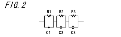
- R1 the intracrystalline resistance of the inorganic solid electrolyte 2
- R2 the grain boundary resistance
- R3 the interface resistance between the inorganic solid electrolyte 2 and the current collector 3
- the inorganic solid electrolyte 2 having a polycrystalline structure is composed of crystal particles 21 with high ion conductivity, but the ion conduction path becomes discontinuous at the interface between the crystal particles 21, that is, the crystal grain boundaries 22. This is because the conduction resistance is increased, and contact resistance and the like are further added to the interface 4 between the inorganic solid electrolyte 2 and the current collector 3.
- the capacitance of the all solid-state capacitor 1 is relatively high in the lowest frequency region of the frequency of the voltage applied to the all solid-state capacitor 1 (hereinafter sometimes simply referred to as “applied voltage”).
- the interfacial capacity at the interface 4 between the inorganic solid electrolyte 2 and the current collector 3 having ion conduction resistance and low frequency response of ions (hereinafter sometimes simply referred to as “interface capacity”) is dominant.
- the content of crystal grains having a relatively low ion conduction resistance and high frequency response of ions (hereinafter sometimes referred to simply as “intra-grain capacity”) is dominant,
- the crystal grain boundary capacity (hereinafter, sometimes simply referred to as “grain boundary capacity”) having the intermediate ion conduction resistance and the intermediate frequency response of the ions is dominant.
- the crystal used as the inorganic solid electrolyte 2 has a fine domain structure 5 composed of a plurality of single crystal regions having different crystal orientations. Since the crystal orientation is different at the domain boundary, ions are scattered and ion conduction resistance is generated. Therefore, when there are many fine domains, there are many boundaries of regions (domains) having different crystal orientations, so that the ionic conductivity inside the crystal is lowered.
- the plurality of crystal particles 21 include first crystal particles 21D, and the first crystal particles 21D have a domain structure 5 composed of a plurality of domains.
- the size of the domain 5B located near the crystal grain boundary 22 of the crystal particle 21 is larger than the size of the domain 5A located near the center of the crystal particle 21. is there. That is, in the first crystal particle 21D, even if the ionic conduction resistance is high due to the fine domain 5A in the vicinity of the center, the boundary between the domains due to the large domain 5B in the vicinity of the crystal grain boundary 22, that is, the outer periphery.
- the ion conductivity of the outer peripheral portion can be maintained high, the relative dielectric constant of the inorganic solid electrolyte 2 can be increased, and the capacitance of the all solid-state capacitor 1 can be increased.
- the domain 5B is located in the vicinity of the crystal grain boundary 22 that at least a part of the domain 5B is adjacent to the crystal grain boundary 22 or other domains existing between the domain 5B and the crystal grain boundary 22 are one. Indicates that there are ⁇ 3.
- the domain structure 5 inside the first crystal particle 21D can be confirmed by, for example, a transmission electron microscope (TEM).
- TEM transmission electron microscope
- the size of the domain 5A located near the center of the crystal particle 21 is approximately 30 nm or less
- the size of the domain 5B located near the crystal grain boundary 22 is equal to the first crystal
- the range varies depending on the size and shape of the particle 21D, but is approximately 30 to 300 nm.
- the domain size basically refers to the size of the domain in the major axis direction, but the domain 5B is adjacent to the crystal grain boundary 22 and the shape thereof has a large aspect ratio of, for example, 3 or more.
- the thickness from the crystal grain boundary 22 to the boundary between the domain 5B and another domain is regarded as the size of the domain 5B.
- ions cannot move from one crystal grain 21 to the other crystal grain 21 adjacent through the crystal grain boundary 22.
- the resistance to ion conduction (grain boundary resistance) between the crystal grains 22 sandwiching the crystal grain boundary 22 increases, the responsiveness of ions moving between the pair of current collectors 3 decreases, and the inorganic solid electrolyte 2
- the polarization frequency of the electric double layer polarization at the interface 4 between the current collector 3 and the current collector 3 is lowered. Therefore, the frequency region in which the polarization at the crystal grain boundary 22 is dominant is relatively widened, and the frequency dependence of the electrostatic capacitance in the all solid-state capacitor 1 is reduced.
- a grain boundary phase having no ion conductivity may exist in the crystal grain boundary 22.
- the grain boundary phase may be either crystalline or amorphous. Examples of such a grain boundary phase include an oxide containing at least one element of Si and Ge.
- the first crystal particle 21D is composed of a crystal phase having different ion conductivity depending on the crystal orientation.
- the crystal orientation with high conductivity is oriented along the crystal grain boundary 22.
- the ion movement direction can be controlled by the crystal orientation.
- the crystal orientation with high ion conductivity is oriented along the crystal grain boundary 22, in other words, the crystal orientation with high ion conductivity is oriented along the outer periphery of the first crystal grain 21D.
- This makes it easier for ions to move along the outer periphery of the first crystal particle 21D and makes it relatively difficult for ions to move in a direction perpendicular to the outer periphery, that is, in a direction crossing the crystal grain boundary 22. . Therefore, in the first crystal particle 21D, the movement of ions between the particles is further suppressed, the grain boundary resistance is further increased, and the frequency region in which the frequency dependence of the capacitance in the all solid-state capacitor 1 is small is further expanded. can do.
- the crystal particle 21 includes a second crystal particle having the domain structure 5 but not having the characteristics of the first crystal particle 21D, or a third crystal particle not having the domain structure.
- the ratio of the first crystal particles 21D in the crystal particles 21 is preferably 30% or more in terms of the ratio of the number of particles.
- the proportion of the first crystal particles 21D in the crystal particles 21 is determined by observing about 20 crystal particles 21 using a transmission electron microscope (TEM), having a domain structure inside the particles, and near the center of the particles.
- TEM transmission electron microscope
- the crystal grains 21 having a larger size of the domain 5B located in the vicinity of the crystal grain boundary 22 than the size of the domain 5A located at the first crystal grain 21D are defined as the first crystal grains with respect to the total number of the observed crystal grains 21. What is necessary is just to calculate the ratio of the number of 21D.
- the first crystal particle 21D preferably has a one-dimensional or two-dimensional ion conduction path.
- Specific examples of such crystals include ⁇ -eucryptite and ⁇ -alumina.
- the ion conductive layer is oriented in the vicinity of the crystal grain boundary 22 in the vicinity of the crystal grain boundary 22 of the first crystal grain 21D, so that ions move along the outer peripheral surface of the particle inside the first crystal grain 21D.
- a superlattice structure against a basic structure with high ion conductivity that has a three-dimensional ion conduction path, anisotropy occurs in ion conductivity, and ion conduction resistance in a specific direction increases. Some behave like a two-dimensional ion conduction path. In this case, the ion conductivity in the basic structure is high, and a relatively high ion conductivity is maintained even when a superlattice structure is formed, which is preferable.
- the elements constituting the A site are two (or more) elements A1 and A2 having different valences and ionic radii
- the presence or absence of the superlattice structure in the perovskite crystal structure can be confirmed by identifying the superlattice peak from the X-ray diffraction (XRD) measurement of the sintered body or observing the crystal particles with a transmission electron microscope (TEM). .
- XRD X-ray diffraction
- TEM transmission electron microscope
- a perovskite crystal structure having such a superlattice structure is, for example, M1 (2-x) / 3 M2 x M3O 3 (where M1 is a rare earth element, M2 is an alkali metal element, and M3 is a tetravalent metal element) Yes, 0 ⁇ x ⁇ 0.5).
- M1 is a rare earth element
- M2 is an alkali metal element
- M3 is a tetravalent metal element
- Yes 0 ⁇ x ⁇ 0.5
- an alkaline earth metal element or an alkali metal element other than M2 or the like is dissolved, so that a crystal orientation with high ion conductivity, that is, a superlattice structure is formed in the vicinity of the crystal grain boundary 22 of the first crystal particle 21D.
- Domains 5 ⁇ / b> B are formed in which the layered structure to be formed is oriented along the crystal grain boundaries 22.
- La 2 / 3-x Li 3x TiO 3 which is a composite oxide containing La, Li and Ti (where x is 0 ⁇
- the sintered body of 3x ⁇ 0.5 (hereinafter sometimes referred to as LLTO) will be specifically described.
- LLTO has La and Li as constituent elements of the A site, and two types of layers appear alternately, a layer in which the A site is mainly composed of La and a layer in which the A site is mainly composed of Li and vacancies. It is easy to take a superlattice structure. In such a superlattice structure with advanced layer separation, the ion conductivity in the layer mainly composed of Li and vacancies is higher than that in the layer mainly composed of La, and ions are arranged in a two-dimensional orientation (in the layer). High conductivity will appear. The domain in this case is a region where the orientation of the superlattice structure is aligned.
- La has the highest luminance among the constituent elements, and therefore observation is performed by irradiating an electron beam from the a-axis and c-axis directions of the crystal lattice. Then, a layer in which La showing the highest luminance is continuously observed, that is, a layer in which the A site is mainly composed of La (La rich layer), and a La poor layer (A site is present between the La rich layers). It can be seen that a layer mainly composed of Li and holes) exists. Li ions move in this La poor layer.
- the inorganic solid electrolyte 2 having a polycrystalline structure can be obtained.
- a part of Ti constituting the B site may be substituted with a pentavalent metal element such as Nb or Ta.
- Such a LLTO sintered body further contains at least one element of the element group consisting of Na, K, Mg, Ca, Sr and Ba, so that the vicinity of the grain boundary 22 of the first crystal grain 21D.
- the domain 5 ⁇ / b> B located in the region has a crystal orientation with high ion conductivity, that is, a layered structure forming a superlattice structure oriented along the crystal grain boundary 22.
- the content of the element group in the LLTO sintered body is preferably 1 to 9% by mass in terms of oxide.
- the thickness of the inorganic solid electrolyte 2 is preferably about several to ten crystal particles 21. Specifically, the thickness of the inorganic solid electrolyte 2 is 0.5 to 20 ⁇ m, preferably 1 to 10 ⁇ m. By making the thickness of the inorganic solid electrolyte 2 in such a range, the variation of the capacitance with respect to the frequency of the voltage applied to the all-solid capacitor 1, that is, the frequency dependency of the capacitance is further reduced. And a stable capacitor can be realized.
- the thickness of the current collector 3 is not particularly limited, but is, for example, 0.5 to 3.0 ⁇ m.
- the all solid-state capacitor 1 is formed by firing, for example, the inorganic solid electrolyte 2 first, and using a metal material such as Au, Ag, Ni, Pd or Cu on the surface of the fired inorganic solid electrolyte 2 using an ion sputtering apparatus or the like.
- a pair of current collectors 3 is formed.
- a current collector paste containing Ag / Pd or Ni is screen-printed on the surface of the solid electrolyte sheet before firing, and after laminating these, the solid electrolyte sheet and the current collector paste are used as a current collector material.
- simultaneous firing is performed in the air (in the case of Ag / Pd) or in a non-oxidizing atmosphere (in the case of Ni).
- the current collector 3 containing Ag when used, it can be fired in the air (in an oxygen atmosphere), so that the manufacturing cost can be reduced.
- the inorganic solid electrolyte 2 can be prepared, for example, by mixing raw material powder of crystal particles 21 having ionic conductivity, primary pulverization, primary calcination, secondary calcination, secondary pulverization, and firing.
- the powder of the oxide and carbonate may be mixed with the raw material powder after secondary grinding, and tertiary grinding may be performed.
- the calcined powder after the primary calcining is preferably subjected to secondary calcining after crushing.
- the primary calcination is performed at a temperature of 800 ° C. and a holding time of 4 hours
- the secondary calcination is performed at a temperature of 1150 ° C. and a holding time of 12 hours
- the baking is performed at a temperature of 1250 ° C.
- An inorganic solid electrolyte made of a sintered body was produced.
- 150 g of isopropyl alcohol (IPA) as a solvent was added to form a slurry, which was pulverized and mixed (primary pulverized) for 15 hours with a rotary mill using ⁇ 10 mm zirconia balls.
- IPA isopropyl alcohol
- the slurry is dried by a rotary evaporator, and subjected to primary calcination in the air at a calcination temperature of 800 ° C. and a holding time of 4 hours, and further in the air at a calcination temperature of 1150 ° C. and a holding time of 12 hours. did.
- the powder obtained after the secondary calcining is crushed in a mortar, and IPA is added again to the crushed powder to form a slurry, and the average particle diameter of the powder is determined by a rotating mill using a zirconia ball having a diameter of 10 mm.
- the mixture was pulverized and mixed (secondary pulverization) until the average particle size was obtained.
- the slurry is dried on a rotary evaporator, and the powder obtained after the secondary pulverization is replaced with any one of 98% pure BaCO 3 powder, 98% pure SrCO 3 powder and 98% pure K 2 CO 3 powder.
- a predetermined amount was mixed with respect to 100% by mass of the powder obtained after the secondary pulverization, and IPA was added to form a slurry, which was pulverized and mixed (tertiary pulverization) for 15 hours with a rotary mill using zirconia balls of ⁇ 10 mm.
- Table 1 shows the addition amounts of BaCO 3 powder, SrCO 3 powder, and K 2 CO 3 powder with respect to 100% by mass of the powder obtained after the secondary pulverization, as oxide equivalent amounts.
- the powder obtained after the tertiary pulverization is mixed with 5% by mass of paraffin wax, and then press-molded with a mold press at a pressure of 1 ton / cm 2 to form a disk having a diameter of 15 mm and a thickness of 1.5 mm.
- a press-molded body was prepared.
- This press-molded body was fired in the air under the conditions of a heating rate of 400 ° C./hour, a firing temperature of 1250 ° C., a holding time of 6 hours, and a cooling rate of 400 ° C./hour, and a disk having a diameter of 13 mm and a thickness of 1.3 mm
- An inorganic solid electrolyte as a sintered body was obtained.
- XRD X-ray diffraction
- Each sample had a perovskite crystal structure of LLTO, and a diffraction peak derived from the superlattice structure was confirmed.
- the obtained inorganic solid electrolyte was subjected to microtome processing, and 20 crystal particles were observed for each sample using a transmission electron microscope (TEM).
- TEM transmission electron microscope
- the size of the domain near the crystal grain boundary and the crystal center was compared, and the first crystal grain having a clearly large domain size near the crystal grain boundary was extracted.
- the ratio of the first crystal particles was calculated from the number.
- the orientation of the domains in the vicinity of the grain boundaries of the first crystal grains was also confirmed.
- the crystal particles had a domain structure, and the domain size in the vicinity of the center of the crystal was approximately 30 nm or less.
- Sample No. In 2 to 6 the domain size near the crystal grain boundary was larger than the domain near the center, and the size was 30 to 300 nm as the thickness from the crystal grain boundary to the domain boundary.
- an impedance measuring device manufactured by Solartron was used in the frequency range of 0.01 Hz to 10 MHz, and an impedance measuring device manufactured by Agilent was used in the frequency range of 40 Hz to 110 MHz (type 4295A).
- An AC voltage having an effective voltage of 500 mV (Bias 0 V) was applied, and the real part Z ′ and the imaginary part Z ′′ of the impedance were measured.
- the capacitance Cp (F) was calculated from the measured real part Z ′ and imaginary part Z ′′, and the relative dielectric constant ⁇ r was calculated.
- Table 1 The evaluation results of each sample are shown in Table 1.
- Table 1 the ratio of relative permittivity at a frequency of 1 Hz to the relative permittivity at a frequency of 1 kHz ( ⁇ r (1 Hz) / ⁇ r (1 kHz)) is shown as the frequency dependence of the relative permittivity. It can be determined that the frequency dependence of the relative permittivity is smaller as the ratio value is closer to “1”, that is, the frequency dependence of the capacitance is smaller.
- ⁇ r (1 kHz) is preferably 1.0 ⁇ 10 4 or more, and if ⁇ r (1 Hz) / ⁇ r (1 kHz) ⁇ 10, it is determined that the frequency dependency is sufficiently small and preferable.
- Sample No. Nos. 2 to 8 include the first crystal particles in the inorganic solid electrolyte, the relative dielectric constant at 1 kHz is 1.0 ⁇ 10 4 or more, and the ratio of the relative dielectric constant of 1 Hz to the relative dielectric constant of 1 kHz is 10 or less. Excellent characteristics were exhibited. On the other hand, Sample No. No. 1 did not contain the first crystal particles, and the ratio of the relative permittivity of 1 Hz to the relative permittivity of 1 kHz was as large as 40, and the frequency dependence of the relative permittivity was large.
- FIG. 1 shows a transmission electron microscope (TEM) photograph of 1 crystal particle. It can be seen that both the vicinity of the center of the crystal grain (a) and the vicinity of the crystal grain boundary (b) are composed of domains having a size of approximately 30 nm or less. Sample No. In 1, all the observed crystal grains had a similar structure. On the other hand, sample No. In FIG. 4, as shown in FIG. 4, the vicinity of the center (a) of the crystal grain is composed of domains having a size of approximately 30 nm or less, but the domain size is relatively large in the vicinity of the grain boundary (b). It can be seen that the crystal orientation with high conductivity is oriented along the grain boundary. 3 and FIG. 4, the solid line arrows indicate the c-axis direction of the crystal orientation in each domain, and the broken line arrows indicate the direction of high ion conductivity.
- TEM transmission electron microscope
- All-solid-state capacitor 2 Inorganic solid electrolyte 21: Crystal particle 21D: First crystal particle 22: Crystal grain boundary 3: Current collector 4: Interface between inorganic solid electrolyte and current collector 5: Domain structure 5A: Region 5B in the vicinity of the center of the crystal grain where a small size domain exists: Domain located in the vicinity of the crystal grain boundary
Landscapes
- Engineering & Computer Science (AREA)
- Chemical & Material Sciences (AREA)
- Ceramic Engineering (AREA)
- Power Engineering (AREA)
- Manufacturing & Machinery (AREA)
- Inorganic Chemistry (AREA)
- Organic Chemistry (AREA)
- Microelectronics & Electronic Packaging (AREA)
- Structural Engineering (AREA)
- Materials Engineering (AREA)
- Chemical Kinetics & Catalysis (AREA)
- Electrochemistry (AREA)
- Thermal Sciences (AREA)
- Physics & Mathematics (AREA)
- Life Sciences & Earth Sciences (AREA)
- Environmental & Geological Engineering (AREA)
- General Life Sciences & Earth Sciences (AREA)
- Geology (AREA)
- Electric Double-Layer Capacitors Or The Like (AREA)
- Conductive Materials (AREA)
Abstract
Description
図1は、本発明の一実施形態に係る全固体型キャパシタ1の構成を概略的に示す断面図である。本実施形態の全固体型キャパシタ1は、無機固体電解質2と、この無機固体電解質2を挟んで設けられる一対の集電体3と、を含んで構成される。集電体3は、たとえば、Au、Ag、Ni、PdおよびCuより選ばれる少なくとも1種以上を主成分とする金属材料によって形成される。集電体3の厚みは、特に限定されるものではないが、たとえば、0.5~3.0μmである。
R1<R2<R3・・・式1
各試料について、X線回折装置で、2θ=10~80°の範囲をCuKα線源にてX線回折測定を行って得られたX線回折(XRD)パターンの結果から、結晶相を同定した。いずれの試料も、LLTOのペロブスカイト型の結晶構造を有しており、超格子構造に由来する回折ピークが確認された。
得られた無機固体電解質をミクロトーム加工し、透過型電子顕微鏡(TEM)を用いて各試料につき20個の結晶粒子を観察した。ドメイン構造が確認できた結晶粒子については、結晶粒界近傍と結晶中心近傍のドメインの大きさを比較し、結晶粒界近傍のドメインのサイズが明らかに大きい第1の結晶粒子を抽出し、その個数から第1の結晶粒子の割合を算出した。同時に、第1の結晶粒子の結晶粒界近傍におけるドメインの配向性も確認した。なお、いずれの試料についても、結晶粒子はドメイン構造を有するものであり、結晶の中心近傍におけるドメインサイズは概ね30nm以下であった。また、試料No.2~6では結晶粒界近傍のドメインサイズが中心近傍のドメインに対して大きく、そのサイズは結晶粒界からドメイン境界までの厚さにして30~300nmであった。
各試料の表裏面を♯500~♯3000のサンドペーパ、および♯6000のダイヤモンドペーストを用いて鏡面研磨して、厚みを0.8~1.2mmとした後、イオンスパッタ装置(JEOL-JFC-1500)を用いて表裏面に、直径1cmのAu電極(集電体)を形成した。

2 :無機固体電解質
21 :結晶粒子
21D:第1の結晶粒子
22 :結晶粒界
3 :集電体
4 :無機固体電解質と集電体との界面
5 :ドメイン構造
5A :結晶粒子の中心近傍であって、サイズの小さいドメインが存在する領域
5B :結晶粒界近傍に位置するドメイン
Claims (9)
- 結晶粒子と、該結晶粒子間に形成された結晶粒界とからなる多結晶構造を有する無機固体電解質と、
該無機固体電解質を挟んで設けられる一対の集電体と、を備える全固体型キャパシタであって、
前記結晶粒子が、イオン伝導性を有する第1の結晶粒子を含み、該第1の結晶粒子は、複数のドメインにより構成されるとともに、前記結晶粒子の中心近傍に位置する前記ドメインのサイズよりも、前記結晶粒子の前記結晶粒界近傍に位置する前記ドメインのサイズが大きいことを特徴とする全固体型キャパシタ。 - 前記第1の結晶粒子が、イオン伝導性が結晶方位により異なる結晶相からなり、
前記結晶粒界近傍に位置する前記ドメインにおいて、イオン伝導性が相対的に高い結晶方位が、前記結晶粒界に沿うように配向していることを特徴とする請求項1に記載の全固体型キャパシタ。 - 前記結晶粒子中における前記第1の結晶粒子の割合が、粒子数の比にして30%以上であることを特徴とする請求項1または2に記載の全固体型キャパシタ。
- 前記第1の結晶粒子が、一次元または二次元のイオン伝導経路を有することを特徴とする請求項1乃至3のいずれかに記載の全固体型キャパシタ。
- 前記結晶粒子が、超格子構造を備えるペロブスカイト型の結晶構造を有することを特徴とする請求項1乃至4のいずれかに記載の全固体型キャパシタ。
- 前記無機固体電解質が、少なくともLi、LaおよびTiを含む複合酸化物の焼結体であることを特徴とする請求項1乃至5のいずれかに記載の全固体型キャパシタ。
- 前記焼結体が、さらにNa、K、Mg、Ca、SrおよびBaからなる元素群のうち少なくとも1種の元素を含むことを特徴とする請求項6に記載の全固体型キャパシタ。
- 前記焼結体における前記元素群の含有量が、酸化物換算にして合計で1~9質量%であることを特徴とする請求項7に記載の全固体型キャパシタ。
- 電気二重層キャパシタであることを特徴とする請求項1乃至8のいずれかに記載の全固体型キャパシタ。
Priority Applications (4)
| Application Number | Priority Date | Filing Date | Title |
|---|---|---|---|
| US15/027,318 US9916937B2 (en) | 2013-10-18 | 2014-09-29 | All-solid-state capacitor |
| CN201480056366.9A CN105706201B (zh) | 2013-10-18 | 2014-09-29 | 全固态型电容器 |
| EP14854440.6A EP3059748B1 (en) | 2013-10-18 | 2014-09-29 | All-solid-state capacitor |
| JP2015508917A JP5781715B1 (ja) | 2013-10-18 | 2014-09-29 | 全固体型キャパシタ |
Applications Claiming Priority (2)
| Application Number | Priority Date | Filing Date | Title |
|---|---|---|---|
| JP2013-217563 | 2013-10-18 | ||
| JP2013217563 | 2013-10-18 |
Publications (1)
| Publication Number | Publication Date |
|---|---|
| WO2015056558A1 true WO2015056558A1 (ja) | 2015-04-23 |
Family
ID=52828007
Family Applications (1)
| Application Number | Title | Priority Date | Filing Date |
|---|---|---|---|
| PCT/JP2014/075959 Ceased WO2015056558A1 (ja) | 2013-10-18 | 2014-09-29 | 全固体型キャパシタ |
Country Status (5)
| Country | Link |
|---|---|
| US (1) | US9916937B2 (ja) |
| EP (1) | EP3059748B1 (ja) |
| JP (1) | JP5781715B1 (ja) |
| CN (1) | CN105706201B (ja) |
| WO (1) | WO2015056558A1 (ja) |
Cited By (5)
| Publication number | Priority date | Publication date | Assignee | Title |
|---|---|---|---|---|
| KR20180103551A (ko) * | 2017-03-10 | 2018-09-19 | 삼성전자주식회사 | 유전체, 그 제조 방법, 이를 포함하는 유전체 소자 및 전자 소자 |
| US10515760B1 (en) | 2018-08-09 | 2019-12-24 | Samsung Electro-Mechanics Co., Ltd. | Multilayer ceramic capacitor with dielectric layers including dielectric grains having a core-shell structure |
| JP2020501332A (ja) * | 2016-09-29 | 2020-01-16 | パリ・シアンス・エ・レットゥル−カルチエ・ラタン | スーパーキャパシタを備えるデバイス及びそのデバイスの製造方法 |
| JP2020021826A (ja) * | 2018-07-31 | 2020-02-06 | サムソン エレクトロ−メカニックス カンパニーリミテッド. | キャパシタ、キャパシタ用固体電解質粒子の製造方法、及び、キャパシタの製造方法 |
| US11823838B2 (en) | 2017-03-31 | 2023-11-21 | Samsung Electronics Co., Ltd. | Two-dimensional perovskite material, dielectric material and multi-layered capacitor including the same |
Families Citing this family (1)
| Publication number | Priority date | Publication date | Assignee | Title |
|---|---|---|---|---|
| WO2014148234A1 (ja) * | 2013-03-18 | 2014-09-25 | 京セラ株式会社 | 全固体型キャパシタ |
Citations (7)
| Publication number | Priority date | Publication date | Assignee | Title |
|---|---|---|---|---|
| JPH0546700B2 (ja) | 1985-07-04 | 1993-07-14 | Hitachi Electr Eng | |
| JPH0859339A (ja) * | 1994-08-18 | 1996-03-05 | Mitsubishi Heavy Ind Ltd | ベータアルミナ電解質 |
| JPH10182220A (ja) * | 1996-12-24 | 1998-07-07 | Osamu Yamamoto | β”−アルミナ基固体電解質とその製造方法 |
| JP2001192260A (ja) * | 1999-10-25 | 2001-07-17 | Ngk Spark Plug Co Ltd | ベータアルミナ質焼結体 |
| JP2008130844A (ja) | 2006-11-21 | 2008-06-05 | Matsushita Electric Ind Co Ltd | 全固体型電気二重層コンデンサー |
| JP2012138502A (ja) | 2010-12-27 | 2012-07-19 | Tdk Corp | 積層セラミックコンデンサ |
| JP2013134812A (ja) * | 2011-12-26 | 2013-07-08 | Sony Corp | 固体電解質、固体電解質の製造方法および電気化学デバイス |
Family Cites Families (8)
| Publication number | Priority date | Publication date | Assignee | Title |
|---|---|---|---|---|
| JP4228560B2 (ja) * | 2000-11-01 | 2009-02-25 | ソニー株式会社 | キャパシタ素子及びその製造方法 |
| JP2004143477A (ja) * | 2002-10-22 | 2004-05-20 | Cabot Supermetal Kk | ニオブ粉末およびその製造方法、並びにそれを用いた固体電解コンデンサ |
| US6829136B2 (en) * | 2002-11-29 | 2004-12-07 | Murata Manufacturing Co., Ltd. | Dielectric ceramic, method for making the same, and monolithic ceramic capacitor |
| US7057876B2 (en) * | 2004-07-29 | 2006-06-06 | Kyocera Corporation | Multilayer ceramic capacitor and manufacturing method thereof |
| JP4502740B2 (ja) * | 2004-07-29 | 2010-07-14 | 京セラ株式会社 | 積層セラミックコンデンサおよびその製法 |
| JP5117033B2 (ja) * | 2006-11-08 | 2013-01-09 | モメンティブ・パフォーマンス・マテリアルズ・ジャパン合同会社 | 光半導体用シリコーン接着剤組成物及びそれを用いた光半導体装置 |
| JP5046700B2 (ja) | 2007-03-27 | 2012-10-10 | 京セラ株式会社 | 誘電体磁器および積層セラミックコンデンサ |
| WO2014148234A1 (ja) * | 2013-03-18 | 2014-09-25 | 京セラ株式会社 | 全固体型キャパシタ |
-
2014
- 2014-09-29 WO PCT/JP2014/075959 patent/WO2015056558A1/ja not_active Ceased
- 2014-09-29 US US15/027,318 patent/US9916937B2/en not_active Expired - Fee Related
- 2014-09-29 EP EP14854440.6A patent/EP3059748B1/en not_active Not-in-force
- 2014-09-29 CN CN201480056366.9A patent/CN105706201B/zh not_active Expired - Fee Related
- 2014-09-29 JP JP2015508917A patent/JP5781715B1/ja not_active Expired - Fee Related
Patent Citations (7)
| Publication number | Priority date | Publication date | Assignee | Title |
|---|---|---|---|---|
| JPH0546700B2 (ja) | 1985-07-04 | 1993-07-14 | Hitachi Electr Eng | |
| JPH0859339A (ja) * | 1994-08-18 | 1996-03-05 | Mitsubishi Heavy Ind Ltd | ベータアルミナ電解質 |
| JPH10182220A (ja) * | 1996-12-24 | 1998-07-07 | Osamu Yamamoto | β”−アルミナ基固体電解質とその製造方法 |
| JP2001192260A (ja) * | 1999-10-25 | 2001-07-17 | Ngk Spark Plug Co Ltd | ベータアルミナ質焼結体 |
| JP2008130844A (ja) | 2006-11-21 | 2008-06-05 | Matsushita Electric Ind Co Ltd | 全固体型電気二重層コンデンサー |
| JP2012138502A (ja) | 2010-12-27 | 2012-07-19 | Tdk Corp | 積層セラミックコンデンサ |
| JP2013134812A (ja) * | 2011-12-26 | 2013-07-08 | Sony Corp | 固体電解質、固体電解質の製造方法および電気化学デバイス |
Cited By (10)
| Publication number | Priority date | Publication date | Assignee | Title |
|---|---|---|---|---|
| JP2020501332A (ja) * | 2016-09-29 | 2020-01-16 | パリ・シアンス・エ・レットゥル−カルチエ・ラタン | スーパーキャパシタを備えるデバイス及びそのデバイスの製造方法 |
| US11170945B2 (en) | 2016-09-29 | 2021-11-09 | Paris Sciences Et Lettres—Quartier Latin | Supercapacitor with electrolyte |
| KR20180103551A (ko) * | 2017-03-10 | 2018-09-19 | 삼성전자주식회사 | 유전체, 그 제조 방법, 이를 포함하는 유전체 소자 및 전자 소자 |
| KR102392041B1 (ko) * | 2017-03-10 | 2022-04-27 | 삼성전자주식회사 | 유전체, 그 제조 방법, 이를 포함하는 유전체 소자 및 전자 소자 |
| US11358904B2 (en) | 2017-03-10 | 2022-06-14 | Samsung Electronics Co., Ltd. | Dielectric material, method of manufacturing thereof, and dielectric devices and electronic devices including the same |
| US11823838B2 (en) | 2017-03-31 | 2023-11-21 | Samsung Electronics Co., Ltd. | Two-dimensional perovskite material, dielectric material and multi-layered capacitor including the same |
| JP2020021826A (ja) * | 2018-07-31 | 2020-02-06 | サムソン エレクトロ−メカニックス カンパニーリミテッド. | キャパシタ、キャパシタ用固体電解質粒子の製造方法、及び、キャパシタの製造方法 |
| JP7151048B2 (ja) | 2018-07-31 | 2022-10-12 | サムソン エレクトロ-メカニックス カンパニーリミテッド. | キャパシタ、キャパシタ用固体電解質粒子の製造方法、及び、キャパシタの製造方法 |
| US10515760B1 (en) | 2018-08-09 | 2019-12-24 | Samsung Electro-Mechanics Co., Ltd. | Multilayer ceramic capacitor with dielectric layers including dielectric grains having a core-shell structure |
| US10748709B2 (en) | 2018-08-09 | 2020-08-18 | Samsung Electro-Mechanics Co., Ltd. | Multilayer ceramic capacitor with dielectric layers including dielectric grains having a core-shell structure |
Also Published As
| Publication number | Publication date |
|---|---|
| US9916937B2 (en) | 2018-03-13 |
| EP3059748A4 (en) | 2017-07-05 |
| EP3059748B1 (en) | 2021-01-13 |
| CN105706201B (zh) | 2018-04-03 |
| CN105706201A (zh) | 2016-06-22 |
| EP3059748A1 (en) | 2016-08-24 |
| JP5781715B1 (ja) | 2015-09-24 |
| JPWO2015056558A1 (ja) | 2017-03-09 |
| US20160247635A1 (en) | 2016-08-25 |
Similar Documents
| Publication | Publication Date | Title |
|---|---|---|
| Liu et al. | Excellent energy storage density and efficiency in lead-free Sm-doped BaTiO 3–Bi (Mg 0.5 Ti 0.5) O 3 ceramics | |
| JP5781715B1 (ja) | 全固体型キャパシタ | |
| JP4991564B2 (ja) | 積層セラミックコンデンサ | |
| CN101687663B (zh) | 半导体陶瓷粉末、半导体陶瓷及层叠型半导体陶瓷电容器 | |
| Si et al. | Structural and dielectric relaxor properties of (1− x) BaTiO3–x Bi (Zn1/2Zr1/2) O3 ceramics for energy storage applications | |
| WO2014002302A1 (ja) | 積層セラミックコンデンサ | |
| JP2016108231A (ja) | 誘電体磁器組成物及びこれを含む積層セラミックキャパシタ | |
| JP6272613B2 (ja) | 全固体型キャパシタ | |
| Qiao et al. | Local order and oxygen ion conduction induced high-temperature colossal permittivity in lead-free Bi0. 5Na0. 5TiO3-based systems | |
| Mao et al. | Low-Temperature Sintering Properties of Bi2O3 Doped PZT-5H Piezoelectric Ceramics: W. Mao et al. | |
| KR20120112173A (ko) | 반도체 세라믹 및 적층형 반도체 세라믹 콘덴서 | |
| CN118197801A (zh) | 介电材料、包括其的器件以及制备该介电材料的方法 | |
| JP2003077754A (ja) | 積層セラミックコンデンサ及びその製法 | |
| WO2023112661A1 (ja) | 圧電/誘電体セラミックス、圧電素子及び発音体 | |
| JP2008297133A (ja) | 誘電体磁器およびコンデンサ | |
| Wang et al. | High permittivity and low dielectric loss of (1-x) Bi0. 5 (Na0. 48K0. 52) 0.5 TiO3-x BaZrO3 lead-free ceramics | |
| JP2016160166A (ja) | 誘電体組成物および電子部品 | |
| JP2015076573A (ja) | 全固体型電気二重層コンデンサ | |
| Cai et al. | Enhancement of energy storage properties of BNBT ceramics modified by tungsten bronze-structured Sr5LaTi3Ta7O30 | |
| JP5094011B2 (ja) | 誘電体磁器 | |
| JP6435157B2 (ja) | 全固体型電気二重層コンデンサ | |
| JP7718584B2 (ja) | セラミックス | |
| Yuan et al. | Effects of ZnO and CeO2 additions on the microstructure and dielectric properties of Mn-modified (Bi0. 5Na0. 5) 0.88 Ca0. 12TiO3 ceramics | |
| JP6113266B2 (ja) | 全固体型キャパシタ | |
| JP2006045046A (ja) | 誘電体磁器組成物及び積層セラミック部品 |
Legal Events
| Date | Code | Title | Description |
|---|---|---|---|
| ENP | Entry into the national phase |
Ref document number: 2015508917 Country of ref document: JP Kind code of ref document: A |
|
| 121 | Ep: the epo has been informed by wipo that ep was designated in this application |
Ref document number: 14854440 Country of ref document: EP Kind code of ref document: A1 |
|
| REEP | Request for entry into the european phase |
Ref document number: 2014854440 Country of ref document: EP |
|
| WWE | Wipo information: entry into national phase |
Ref document number: 15027318 Country of ref document: US Ref document number: 2014854440 Country of ref document: EP |
|
| NENP | Non-entry into the national phase |
Ref country code: DE |