WO2015068802A1 - Substrat mère, élément de commande de lumière, procédé de fabrication d'un élément de commande de lumière, et dispositif d'affichage - Google Patents
Substrat mère, élément de commande de lumière, procédé de fabrication d'un élément de commande de lumière, et dispositif d'affichage Download PDFInfo
- Publication number
- WO2015068802A1 WO2015068802A1 PCT/JP2014/079581 JP2014079581W WO2015068802A1 WO 2015068802 A1 WO2015068802 A1 WO 2015068802A1 JP 2014079581 W JP2014079581 W JP 2014079581W WO 2015068802 A1 WO2015068802 A1 WO 2015068802A1
- Authority
- WO
- WIPO (PCT)
- Prior art keywords
- light
- region
- control member
- base material
- shielding layer
- Prior art date
- Legal status (The legal status is an assumption and is not a legal conclusion. Google has not performed a legal analysis and makes no representation as to the accuracy of the status listed.)
- Ceased
Links
Images














Classifications
-
- G—PHYSICS
- G02—OPTICS
- G02B—OPTICAL ELEMENTS, SYSTEMS OR APPARATUS
- G02B5/00—Optical elements other than lenses
- G02B5/02—Diffusing elements; Afocal elements
- G02B5/0273—Diffusing elements; Afocal elements characterized by the use
- G02B5/0278—Diffusing elements; Afocal elements characterized by the use used in transmission
-
- G—PHYSICS
- G02—OPTICS
- G02B—OPTICAL ELEMENTS, SYSTEMS OR APPARATUS
- G02B5/00—Optical elements other than lenses
- G02B5/003—Light absorbing elements
-
- G—PHYSICS
- G02—OPTICS
- G02B—OPTICAL ELEMENTS, SYSTEMS OR APPARATUS
- G02B5/00—Optical elements other than lenses
- G02B5/02—Diffusing elements; Afocal elements
- G02B5/0205—Diffusing elements; Afocal elements characterised by the diffusing properties
- G02B5/0236—Diffusing elements; Afocal elements characterised by the diffusing properties the diffusion taking place within the volume of the element
-
- G—PHYSICS
- G02—OPTICS
- G02B—OPTICAL ELEMENTS, SYSTEMS OR APPARATUS
- G02B5/00—Optical elements other than lenses
- G02B5/02—Diffusing elements; Afocal elements
- G02B5/0268—Diffusing elements; Afocal elements characterized by the fabrication or manufacturing method
-
- G—PHYSICS
- G02—OPTICS
- G02B—OPTICAL ELEMENTS, SYSTEMS OR APPARATUS
- G02B5/00—Optical elements other than lenses
- G02B5/20—Filters
- G02B5/201—Filters in the form of arrays
-
- G—PHYSICS
- G02—OPTICS
- G02B—OPTICAL ELEMENTS, SYSTEMS OR APPARATUS
- G02B5/00—Optical elements other than lenses
- G02B5/20—Filters
- G02B5/208—Filters for use with infrared or ultraviolet radiation, e.g. for separating visible light from infrared and/or ultraviolet radiation
-
- G—PHYSICS
- G02—OPTICS
- G02F—OPTICAL DEVICES OR ARRANGEMENTS FOR THE CONTROL OF LIGHT BY MODIFICATION OF THE OPTICAL PROPERTIES OF THE MEDIA OF THE ELEMENTS INVOLVED THEREIN; NON-LINEAR OPTICS; FREQUENCY-CHANGING OF LIGHT; OPTICAL LOGIC ELEMENTS; OPTICAL ANALOGUE/DIGITAL CONVERTERS
- G02F1/00—Devices or arrangements for the control of the intensity, colour, phase, polarisation or direction of light arriving from an independent light source, e.g. switching, gating or modulating; Non-linear optics
- G02F1/01—Devices or arrangements for the control of the intensity, colour, phase, polarisation or direction of light arriving from an independent light source, e.g. switching, gating or modulating; Non-linear optics for the control of the intensity, phase, polarisation or colour
- G02F1/13—Devices or arrangements for the control of the intensity, colour, phase, polarisation or direction of light arriving from an independent light source, e.g. switching, gating or modulating; Non-linear optics for the control of the intensity, phase, polarisation or colour based on liquid crystals, e.g. single liquid crystal display cells
- G02F1/133—Constructional arrangements; Operation of liquid crystal cells; Circuit arrangements
- G02F1/1333—Constructional arrangements; Manufacturing methods
- G02F1/1335—Structural association of cells with optical devices, e.g. polarisers or reflectors
- G02F1/133504—Diffusing, scattering, diffracting elements
-
- G—PHYSICS
- G02—OPTICS
- G02F—OPTICAL DEVICES OR ARRANGEMENTS FOR THE CONTROL OF LIGHT BY MODIFICATION OF THE OPTICAL PROPERTIES OF THE MEDIA OF THE ELEMENTS INVOLVED THEREIN; NON-LINEAR OPTICS; FREQUENCY-CHANGING OF LIGHT; OPTICAL LOGIC ELEMENTS; OPTICAL ANALOGUE/DIGITAL CONVERTERS
- G02F1/00—Devices or arrangements for the control of the intensity, colour, phase, polarisation or direction of light arriving from an independent light source, e.g. switching, gating or modulating; Non-linear optics
- G02F1/01—Devices or arrangements for the control of the intensity, colour, phase, polarisation or direction of light arriving from an independent light source, e.g. switching, gating or modulating; Non-linear optics for the control of the intensity, phase, polarisation or colour
- G02F1/13—Devices or arrangements for the control of the intensity, colour, phase, polarisation or direction of light arriving from an independent light source, e.g. switching, gating or modulating; Non-linear optics for the control of the intensity, phase, polarisation or colour based on liquid crystals, e.g. single liquid crystal display cells
- G02F1/133—Constructional arrangements; Operation of liquid crystal cells; Circuit arrangements
- G02F1/1333—Constructional arrangements; Manufacturing methods
- G02F1/1335—Structural association of cells with optical devices, e.g. polarisers or reflectors
- G02F1/1336—Illuminating devices
- G02F1/133602—Direct backlight
- G02F1/133606—Direct backlight including a specially adapted diffusing, scattering or light controlling members
Definitions
- the present invention relates to a mother substrate, a light control member, a method for manufacturing a light control member, and a display device.
- This application claims priority on November 8, 2013 based on Japanese Patent Application No. 2013-232418 for which it applied to Japan, and uses the content for it here.
- Liquid crystal display devices are widely used as displays for portable electronic devices such as cellular phones, televisions, personal computers, and the like.
- a liquid crystal display device is excellent in visibility from the front, but has a narrow viewing angle. Therefore, various devices have been made to widen the viewing angle.
- a configuration has been proposed in which a member for controlling the diffusion angle of light emitted from a display body such as a liquid crystal panel (hereinafter referred to as a light diffusion member) is provided on the viewing side of the display body.
- Patent Document 1 discloses a light control member in which a light diffusion layer is provided with a groove having a V-shaped cross section, and a light absorption layer is provided in a part of the groove.
- transparent sheets made of polyethylene terephthalate (PET) or the like are disposed on the light incident side and the light emission side of the light diffusion layer. A part of the light incident perpendicular to the light diffusion layer is totally reflected on the wall surface of the groove and then emitted. Thereby, the light emitted from the light control member is diffused.
- PET polyethylene terephthalate
- a transparent negative resist is applied with a predetermined film thickness on a long base material to form a light diffusion portion, and the base material is wound up by a winding roller. It will be.
- the transparent negative resist layer it is necessary to form it with a width narrower than the width of the substrate (width in the short direction) so as not to contaminate the back surface of the substrate or the laminating apparatus.
- the base material is wound after the light diffusion portion is formed, the load is concentrated on the step portion generated between the both end portions of the base material and the light diffusion portion, and the light diffusion portion is deformed.
- One aspect of the present invention is made in view of the above-mentioned problems of the prior art, and is a mother base, a light control member, and a light control member that have excellent optical characteristics by suppressing defects that occur in the manufacturing process.
- One of the objects is to provide a manufacturing method and a display device.
- the mother base material has a light-transmitting first base material provided with a light control member forming region, a light shielding layer provided in the first region in the light control member forming region, A plurality of light diffusing portions made of a light transmitting material provided in a region other than the light shielding layer in the first region, and a second region located outside the first region in the light control member forming region.
- the light diffusing portion includes a light emitting end surface located at an end portion on the first surface side of the first base material, and an area of the light emitting end surface with respect to the light emitting end surface.
- a light incident end face having a larger area than the light incident end face, and a reflecting surface that is in contact with the light emitting end face and reflects the light incident from the light incident end face, and has a unit area in the second region
- the formation area of the light transmission material per hit is in the first region It is larger than the forming area of the light transmitting material per position area.
- the light shielding layer is provided in the second region, and the UV transmittance of the light shielding layer provided in the second region is provided in the first region.
- the UV light transmittance of the light shielding layer may be higher.
- the width of the light transmissive material in the second region in plan view may be wider than the arrangement interval of the light shielding layers in the first region.
- the light shielding layer is provided in the second region, and the size of the light shielding layer provided in the second region in plan view is the first region. It is good also as a structure smaller than the magnitude
- a plurality of the light shielding layers may be provided only in the first region.
- the first region may be surrounded by the second region.
- the first surface of the first base material is provided with a third region outside the second region, where the light shielding layer and the light transmitting material are not present. It is good also as a structure currently provided.
- a second base material is disposed opposite to the first surface of the first base material via the light transmitting material, and the light transmitting material and the second base material are disposed. It is good also as a structure by which the elastic member is arrange
- the light control member of one aspect of the present invention includes a light-transmitting first base material, a light shielding layer provided in a first region on the first surface of the first base material, and the first region.
- a light diffusing portion made of a light transmissive material provided in a region other than the light shielding layer, and the light transmissive material provided in a second region located outside the first region on the first surface,
- the light diffusing portion includes a light emitting end face that is in contact with the first surface of the first base material, a light incident end face that has an area larger than an area of the light emitting end face with respect to the light emitting end face, and the light emitting end face And a reflective surface that is in contact with the light incident end surface and reflects light incident from the light incident end surface, and the formation area of the light transmitting material per unit area in the second region is the first region Larger than the formation area of the light transmitting material per unit area in .
- mode of this invention manufactures the several light control member from the mother base material which has several light control member formation area
- a method comprising: forming a light shielding layer in a first region of the plurality of first surfaces; the first region in which the light shielding layer is formed; and a second region located outside the first region.
- the first substrate may be cut in the second region.
- the first base material is transported in a roll-to-roll manner, and the inner side of both ends in a direction intersecting the transport direction of the first base material. It is good also as a manufacturing method which forms a photosensitive resin layer.
- a display device includes a display body that outputs an image in response to an input signal, and a light control member that is provided on the viewing side of the display body and diffuses and emits light incident from the display body.
- the light control member is configured by the light control member, and the light control member includes a first region where the light diffusion portion is formed positioned in a display region of the display body, and the light transmission member. The second region where the material is formed is provided so as to be located in a region other than the display region.
- the light control member is configured to have anisotropy in the light scattering characteristics, and the display body has a relatively narrow luminance viewing angle in an azimuth angle direction,
- the light control member may have a configuration in which the azimuth direction in which the diffusibility of the light control member is relatively strong substantially matches.
- the mother base material and the light control member of one aspect of the present invention it is possible to provide a mother base material and a light control member that have excellent optical characteristics while suppressing problems caused in the manufacturing process.
- the method for manufacturing a light control member of one aspect of the present invention it is possible to provide a light control member having excellent optical characteristics while suppressing defects during the manufacturing process.
- the display device of one aspect of the present invention it is possible to provide a display device having excellent display quality.
- Sectional drawing which shows schematic structure of a liquid crystal display device.
- Sectional drawing which shows schematic structure of a liquid crystal panel.
- the schematic diagram of a light control member The upper left side is a plan view of the light control member, the lower left side is a cross-sectional view taken along the line AA of the upper left side plan view, and the upper right side is a cross-sectional view taken along the line BB of the plan view of the upper left side.
- the flowchart which shows the manufacturing method of a light control member.
- FIG. 8 is a second diagram illustrating a configuration in which a light shielding layer is provided in the second region.
- the top view which illustrates the structure which provided the light shielding layer with a thin film thickness in the 2nd area
- Sectional drawing which compares the film thickness of the light shielding layer in a 1st area
- the top view which shows schematic structure of the light control member in 3rd Embodiment.
- the top view which shows the light control member after cutting out the 3rd field.
- the 1st figure explaining the manufacturing process of the light-control member in 3rd Embodiment.
- the 2nd figure explaining the manufacturing process of the light-control member in 3rd Embodiment.
- Sectional drawing which shows schematic structure of the light control member in 4th Embodiment.
- the schematic block diagram which shows an example of the manufacturing apparatus of the light control member in 5th Embodiment.
- the upper part is a plan view showing a light shielding layer having a rectangular planar shape
- the lower part is a sectional view taken along the line AA of the plan view.
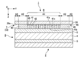
- FIG. 1 is a cross-sectional view showing a schematic configuration of the liquid crystal display device 1.
- the liquid crystal display device 1 includes a backlight 2, a first polarizing plate 3, a liquid crystal panel 4, a second polarizing plate 5, a light control member 7 including a light control member described later, It has.
- the backlight 2, the first polarizing plate 3, the liquid crystal panel 4 and the second polarizing plate 5 constitute a liquid crystal display body (display body) 8.
- the observer sees the display from the upper side of the liquid crystal display device 1 in FIG. 1 where the light control member 7 is arranged.
- the side on which the light control member 7 is disposed is referred to as the viewing side
- the side on which the backlight 2 is disposed is referred to as the back side.
- the X axis is defined as the horizontal direction of the screen of the liquid crystal display device 1
- the Y axis is defined as the vertical direction of the screen of the liquid crystal display device 1
- the Z axis is defined as the thickness direction of the liquid crystal display device 1.
- the light emitted from the backlight 2 is modulated by the liquid crystal panel 4, and a predetermined image, character, or the like is displayed by the modulated light. Further, when the light emitted from the liquid crystal panel 4 passes through the light control member 7, the light distribution (diffusion angle distribution) of the emitted light becomes wider than before entering the light control member 7, so that the light is emitted. Injected from the control member 7. Thereby, the observer can visually recognize the display with a wide viewing angle.
- liquid crystal panel 4 an active matrix transmissive liquid crystal panel will be described as an example.
- a liquid crystal panel applicable to the present invention is not limited to an active matrix transmissive liquid crystal panel.
- the liquid crystal panel applicable to the present invention may be, for example, a transflective type (transmission / reflection type) liquid crystal panel.
- a simple matrix type liquid crystal panel in which each pixel does not include a switching thin film transistor hereinafter abbreviated as TFT may be used.
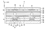
- FIG. 2 is a cross-sectional view showing a schematic configuration of the liquid crystal panel.
- the liquid crystal panel 4 includes a TFT substrate (also referred to as an element substrate) 9, a color filter substrate (also referred to as a counter substrate) 10 disposed to face the TFT substrate 9, and a TFT substrate 9. And a liquid crystal layer 11 disposed between the color filter substrate 10 and the color filter substrate 10.
- the liquid crystal layer 11 seals the periphery between the TFT substrate 9 and the color filter substrate 10 with a seal member (not shown), and injects liquid crystal therebetween, thereby the TFT substrate 9 and the color filter substrate 10. Is sandwiched between.
- a spherical spacer 12 is disposed between the TFT substrate 9 and the color filter substrate 10 in order to keep the distance therebetween constant.
- a plurality of pixels as a minimum unit area for display are arranged in a matrix.
- a plurality of source bus lines (not shown) are formed on the TFT substrate 9 so as to extend in parallel with each other, and a plurality of gate bus lines (not shown) extend in parallel with each other, In addition, it is formed to be orthogonal to a plurality of source bus lines. Therefore, on the TFT substrate 9, a plurality of source bus lines and a plurality of gate bus lines are formed in a lattice pattern, and a rectangular region partitioned by adjacent source bus lines and adjacent gate bus lines is one. One pixel.
- the source bus line is connected to the source electrode of the TFT described later, and the gate bus line is connected to the gate electrode of the TFT.
- a TFT 19 having a semiconductor layer 15, a gate electrode 16, a source electrode 17, a drain electrode 18, etc. is formed on the surface of the transparent substrate 14 constituting the TFT substrate 9 on the liquid crystal layer 11 side.
- a transparent substrate 14 for example, a glass substrate can be used.
- a semiconductor material such as CGS (Continuous Grain Silicon), LPS (Low-temperature Poly-Silicon), ⁇ -Si (Amorphous Silicon) is used.
- a semiconductor layer 15 is formed.
- a gate insulating film 20 is formed on the transparent substrate 14 so as to cover the semiconductor layer 15.
- a material of the gate insulating film 20 for example, a silicon oxide film, a silicon nitride film, or a laminated film thereof is used.
- a gate electrode 16 is formed on the gate insulating film 20 so as to face the semiconductor layer 15.
- a laminated film of W (tungsten) / TaN (tantalum nitride), Mo (molybdenum), Ti (titanium), Al (aluminum), or the like is used.
- a first interlayer insulating film 21 is formed on the gate insulating film 20 so as to cover the gate electrode 16.
- the material of the first interlayer insulating film 21 for example, a silicon oxide film, a silicon nitride film, or a laminated film thereof is used.
- a source electrode 17 and a drain electrode 18 are formed on the first interlayer insulating film 21.
- the source electrode 17 is connected to the source region of the semiconductor layer 15 through a contact hole 22 that penetrates the first interlayer insulating film 21 and the gate insulating film 20.
- the drain electrode 18 is connected to the drain region of the semiconductor layer 15 through a contact hole 23 that penetrates the first interlayer insulating film 21 and the gate insulating film 20.
- the same conductive material as that for the gate electrode 16 is used.
- a second interlayer insulating film 24 is formed on the first interlayer insulating film 21 so as to cover the source electrode 17 and the drain electrode 18.
- the same material as the first interlayer insulating film 21 described above or an organic insulating material is used.
- a pixel electrode 25 is formed on the second interlayer insulating film 24.
- the pixel electrode 25 is connected to the drain electrode 18 through a contact hole 26 that penetrates the second interlayer insulating film 24. That is, the pixel electrode 25 is connected to the drain region of the semiconductor layer 15 using the drain electrode 18 as a relay electrode.
- a transparent conductive material such as ITO (Indium Tin Oxide) or IZO (Indium Zinc Oxide) is used.
- an alignment film 27 is formed over the entire surface so as to cover the pixel electrode 25.
- the alignment film 27 has an alignment regulating force for aligning liquid crystal molecules constituting the liquid crystal layer 11 at an arbitrary orientation and angle by performing a special treatment such as rubbing.
- the form of the TFT may be a top gate TFT shown in FIG. 2 or a bottom gate TFT.
- a black matrix 30, a color filter 31, a planarizing layer 32, a counter electrode 33, and an alignment film 34 are sequentially formed on the surface of the transparent substrate 29 constituting the color filter substrate 10 on the liquid crystal layer 11 side.
- the black matrix 30 has a function of blocking light transmission in the inter-pixel region, and is a photo in which metal such as Cr (chromium) or Cr / Cr oxide multilayer film or carbon particles are dispersed in a photosensitive resin. It is made of resist.
- the color filter 31 includes dyes of red (R), green (G), and blue (B), and one pixel electrode 25 on the TFT substrate 9 is any one of R, G, and B. Two color filters 31 are arranged to face each other.
- the color filter 31 may have a multicolor configuration of three or more colors of R, G, and B.
- the flattening layer 32 is made of an insulating film that covers the black matrix 30 and the color filter 31, and has a function of smoothing and flattening a step formed by the black matrix 30 and the color filter 31.
- a counter electrode 33 is formed on the planarization layer 32. As the material of the counter electrode 33, a transparent conductive material similar to that of the pixel electrode 25 is used. A rubbing process is performed on the entire surface of the counter electrode 33 to form an alignment film 34 having a horizontal alignment regulating force.
- the light control member 7 in this embodiment is composed of a light control member 13 described below.
- the light control member 13 includes a base material (first base material) 39, a plurality of light shielding layers 40, and a light diffusion layer 46.
- the light diffusion layer 46 mainly includes a light diffusion portion 41 and a support portion (light transmission material) 45.
- the light diffusion portion 41 is formed in a region other than the region where the light shielding layer 40 is formed in the first region A1 on the inner surface (first surface) 39a.
- the support portion 45 is formed in the second region A2 located outside the first region A1, and is formed integrally with the light diffusion portion 41 with the same material (light transmission material) as the light diffusion portion 41.
- the light control member 13 is disposed on the second polarizing plate 5 in such a posture that the side where the light diffusing portion 41 is provided faces the second polarizing plate 5 and the base 39 side faces the viewing side.
- the light control member 13 is fixed to the second polarizing plate 5 via an adhesive layer (not shown).
- the base material 39 examples include transparent resin base materials such as triacetyl cellulose (TAC) film, polyethylene terephthalate (PET), polycarbonate (PC), polyethylene naphthalate (PEN), and polyethersulfone (PES) film.
- TAC triacetyl cellulose
- PET polyethylene terephthalate
- PC polycarbonate
- PEN polyethylene naphthalate
- PES polyethersulfone
- the base material 39 becomes a base when the material for the light shielding layer 40 and the light diffusion portion 41 is applied later in the manufacturing process.
- the base material 39 needs to have heat resistance and mechanical strength in a heat treatment step during the manufacturing process. Therefore, as the base material 39, a glass base material or the like may be used in addition to the resin base material. However, it is preferable that the thickness of the base material 39 is as thin as possible without impairing heat resistance and mechanical strength.
- the total light transmittance of the base material 39 is preferably 90% or more as defined in JIS K7361-1. When the total light transmittance is 90% or more, sufficient transparency can be obtained.
- a transparent resin substrate having a thickness of 100 ⁇ m is used as an example.
- the light shielding layer 40 is randomly arranged as viewed from the normal direction of the main surface of the base material 39. Arrangement of the interval (pitch) between the adjacent light shielding layers 40 is neither regular nor periodic. The interval (pitch) between the light shielding layers 40 is preferably smaller than the interval (pitch, for example, 150 ⁇ m) between the pixels of the liquid crystal panel 4. Thereby, at least one light shielding layer 40 is formed in the pixel. Therefore, for example, even when combined with a liquid crystal panel having a small pixel pitch used for a mobile device or the like, a wide viewing angle can be uniformly achieved in the plane.
- the light shielding layer 40 is made of an organic material having light absorption and photosensitivity such as black resist and black ink as an example.
- a metal film such as Cr (chromium) or a Cr / Cr oxide multilayer film may be used.
- the organic material which comprises the light shielding layer 40 may contain the ultraviolet absorber which absorbs an ultraviolet-ray.
- the light diffusing section 41 is made of an organic material having optical transparency and photosensitivity such as acrylic resin and epoxy resin. Further, the total light transmittance of the light diffusing portion 41 is preferably 90% or more in accordance with JIS K7361-1. When the total light transmittance is 90% or more, sufficient transparency can be obtained.
- the light diffusing section 41 has a light exit end face 41a, a light incident end face 41b, and a reflective face 41c.
- the light emission end surface 41 a is a surface in contact with the base material 39.
- the light incident end surface 41b is a surface facing the light emitting end surface 41a.
- the reflection surface 41 c is a tapered side surface of the light diffusion portion 41.
- the reflection surface 41c is a surface that reflects light incident from the light incident end surface 41b.
- the area of the light incident end face 41b is larger than the area of the light exit end face 41a.
- the light diffusion part 41 is a part that contributes to the transmission of light in the light control member 13. That is, the light incident on the light diffusing unit 41 is totally reflected by the reflection surface 41 c of the light diffusing unit 41, and is guided and emitted while being substantially confined inside the light diffusing unit 41.
- the light control member 13 is disposed so that the base material 39 faces the viewing side. Therefore, of the two opposing surfaces of the light diffusing portion 41, the surface with the smaller area becomes the light emission end surface 41a. On the other hand, the surface with the larger area becomes the light incident end surface 41b.
- the inclination angle of the reflection surface 41c of the light diffusion portion 41 (the angle formed between the light incident end surface 41b and the reflection surface 41c) is preferably 75 ° or more and 89 ° or less. In the present embodiment, the inclination angle of the reflection surface 41c of the light diffusion portion 41 is 75 °. However, the inclination angle of the reflection surface 41c of the light diffusing portion 41 is not particularly limited as long as it is an angle that can sufficiently diffuse incident light when light is emitted from the light control member 13. In the present embodiment, the inclination angle of the reflection surface 41c of the light diffusing unit 41 is constant.
- the height from the light incident end surface 41 b to the light emitting end surface 41 a of the light diffusion portion 41 is set to be larger than the layer thickness of the light shielding layer 40.
- the layer thickness of the light shielding layer 40 is about 150 nm as an example.
- the height from the light incident end surface 41b of the light diffusion portion 41 to the light emitting end surface 41a is about 20 ⁇ m.
- a portion surrounded by the reflection surface 41 c of the light diffusion portion 41 and the light shielding layer 40 is a hollow portion 42.
- air exists in the hollow portion 42 (outside the light diffusion portion 41). Therefore, if the light diffusion portion 41 is formed of, for example, a transparent acrylic resin, the reflection surface 41c of the light diffusion portion 41 becomes an interface between the transparent acrylic resin and air.
- the hollow portion 42 may be filled with another low refractive index material. However, the difference in the refractive index at the interface between the inside and the outside of the light diffusing portion 41 is maximized when air is present rather than when any low refractive index material is present outside.
- the critical angle is the smallest in the configuration of the present embodiment, and the incident angle range in which the light is totally reflected by the reflection surface 41c of the light diffusion portion 41 is the widest. As a result, light loss is further suppressed, and high luminance can be obtained.
- the presence of a low refractive index material indicates that the periphery of the light diffusion portion 41 is in a low refractive index state so that light can be totally reflected.
- the hollow portion 42 includes a state in which an inert gas such as nitrogen is filled instead of air.
- the inside of the hollow portion 42 may be in a vacuum state or a reduced pressure state than the atmosphere.
- the refractive index of the base material 39 and the refractive index of the light diffusion portion 41 are substantially equal.
- the reason is as follows. For example, consider a case where the refractive index of the base material 39 and the refractive index of the light diffusion portion 41 are greatly different. In this case, when light incident from the light incident end surface 41 b exits from the light diffusion portion 41, unnecessary light refraction or reflection may occur at the interface between the light diffusion portion 41 and the base material 39. In this case, there is a possibility that problems such as failure to obtain a desired viewing angle and a decrease in the amount of emitted light may occur.
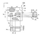
- FIG. 3 is a schematic diagram of the light control member 13.
- the upper left side is a plan view of the light control member 13.
- the lower left side is a cross-sectional view along the line AA in the plan view of the upper left side.
- the upper right stage is a cross-sectional view along the line BB in the plan view of the upper left stage.
- a plurality of light shielding layers 40 are provided on the inner surface 39 a of the base material 39.
- the planar shape of the light shielding layer 40 as viewed from the normal direction of the substrate 39 is an elongated ellipse.
- the light shielding layer 40 has a major axis and a minor axis.
- the long axis is the longest axis in the planar shape of the light shielding layer 40 viewed from the normal direction of the substrate 39.
- the short axis is the shortest axis in the planar shape of the light shielding layer 40 as viewed from the normal direction of the substrate 39.
- the ratio of the length of the short axis to the length of the long axis in each light shielding layer 40 is approximately equal.
- the part corresponding to the lower part of the light shielding layer 40 is an elliptic frustum-shaped hollow part 42.
- the light control member 13 has a plurality of hollow portions 42.
- a light diffusing portion 41 is continuously provided in a portion other than the plurality of hollow portions 42.
- the major axis direction of the ellipse forming the planar shape of each light shielding layer 40 (hereinafter, sometimes referred to as the major axis direction of the light shielding layer 40) is generally aligned in the X direction.
- the minor axis direction of the ellipse forming the planar shape of each light shielding layer 40 (hereinafter, sometimes referred to as the minor axis direction of the light shielding layer 40) is generally aligned in the Y direction.
- the ratio of the reflection surface 41c along the X direction out of the reflection surface 41c of the light diffusion portion 41 is the proportion of the reflection surface 41c along the Y direction. More than. Therefore, the light Ly reflected by the reflecting surface 41c along the X direction and diffused in the Y direction is larger than the light Lx reflected by the reflecting surface 41c along the Y direction and diffused in the X direction.
- the azimuth angle direction Vs in which the light control member 13 has the strongest diffusibility is the Y direction, which is the minor axis direction of the light shielding layer 40.
- the polar angle direction is arbitrary. The definition of polar angle and azimuth will be described later.
- the ratio of the reflective surface along the X direction in the reflective surface 41c of the light diffusing portion 41 is equal to the ratio of the reflective surface along the Y direction.
- the light reflected by the reflecting surface along the X direction and diffused in the Y direction is equal to the light reflected by the reflecting surface along the Y direction and diffused in the X direction. That is, when viewed from the normal direction of the base material 39, the light is reflected isotropically from the reflecting surface 41c. Therefore, there is no azimuthal direction in which the light diffusing portion 41 has the strongest diffusibility.
- FIG. 5 is a plan view schematically showing a schematic configuration of the light control member, as viewed from the light diffusion portion side.
- the plurality of light shielding layers 40 are regularly arranged with the same size, but in actuality, the planar shape is randomly formed in an elongated oval shape.
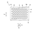
- the light control member 13 includes a plurality of light shielding layers 40 formed in the first region A ⁇ b> 1 on the one surface 39 a of the base material 39, and a light diffusion portion 41 formed so as to surround the plurality of light shielding layers 40. And a support portion 45 formed in the second region A2.
- a large number of light shielding layers 40 are formed only in the first region A ⁇ b> 1 set on one surface 39 a of the base material 39.
- the light diffusion portion 41 is formed in a region other than the region where the light shielding layer 40 is formed in the first region A1.
- the light diffusing portion 41 has a configuration having a hollow portion 42 at a position corresponding to the light shielding layer 40. In the state of the light control member 13 alone, the hollow portion 42 opens on the surface of the light diffusion portion 41 opposite to the base 39 (the surface on the liquid crystal panel 4 side during assembly).
- the support portion 45 is provided in each of the second regions A2 located on both outer sides in the short direction of the first region A1, and has an integrated structure with the light diffusion portion 41.
- the support portion 45 is formed on the inner side than both ends of the base 39 in the short side direction.
- neither the light shielding layer 40 nor the support portion 45 is formed, and a part of the inner surface 39a is exposed.
- the width in the Y direction of the support portion 45 in the second region A2 is wider than the width of the light diffusion portion 41 existing between the hollow portions 42 (maximum separation distance between adjacent light shielding layers 40). Since the light shielding layer 40 is not formed in the second region A2, the hollow portion 42 does not exist. That is, the formation area of the support portion 45 per unit area in the second region A2 is configured to be larger than the formation area of the light diffusion portion 41 per unit area in the first region A1.
- 6A and 6B are schematic diagrams for explaining the operation of the liquid crystal panel 4.
- 6A is a diagram showing a state when no voltage is applied to the liquid crystal panel 4 (between the pixel electrode 25 and the counter electrode 33 shown in FIG. 2) (when no voltage is applied).
- FIG. 6B is a diagram illustrating a state when a certain voltage is applied to the liquid crystal panel 4 (when a voltage is applied).
- the symbol M is a liquid crystal molecule that constitutes the liquid crystal layer 11.
- the transmission axis P1 of the first polarizing plate 3 and the transmission axis of the second polarizing plate 5 are arranged in a crossed Nicols manner.
- the liquid crystal molecules M are twisted by 90 ° between the alignment film 27 and the alignment film 34 as shown in FIG. 6A.
- the polarization plane of linearly polarized light transmitted through the first polarizing plate 3 having the transmission axis P1 in the 135 ° to 315 ° direction is rotated by 90 ° due to the optical rotation of the liquid crystal layer 11.
- the linearly polarized light transmitted through the first polarizing plate 3 is transmitted through the second polarizing plate 5 having the transmission axis P2 in the 45 ° -225 ° direction.
- white display is obtained when no voltage is applied.
- the liquid crystal molecules M rise in a direction along the electric field between the alignment film 27 and the alignment film 34 as shown in FIG. 6B.
- the polarization plane of the linearly polarized light transmitted through the first polarizing plate 3 having the transmission axis P1 in the 135 ° to 315 ° direction does not rotate.
- the linearly polarized light transmitted through the first polarizing plate 3 does not pass through the second polarizing plate 5 having the transmission axis P2 in the 45 ° -225 ° direction.
- black is displayed when a voltage is applied.
- the liquid crystal panel 4 can switch between white display and black display by controlling application / non-application of voltage for each pixel and display an image.
- FIG. 7 is a diagram for explaining the definition of the polar angle and the azimuth angle.
- an angle formed by an observer's line-of-sight direction F with reference to the normal direction E of the screen of the liquid crystal display device 1 is a polar angle ⁇ .
- the angle formed by the direction of the line segment G when the line-of-sight direction F of the observer is projected on the screen with reference to the positive direction (0 ° direction) of the x-axis is defined as an azimuth angle ⁇ .
- FIG. 8A is a front view of the liquid crystal display device
- FIG. 8B is a front view of the liquid crystal display device 1 in which the light control member 13 has a relatively strong azimuthal direction Vs and a transmission axis of the polarizing plate ( It is a figure which shows the arrangement
- the horizontal direction is the azimuth angle ⁇ : 0 ° -180 ° direction.
- the direction of the azimuth angle ⁇ : 0 ° -180 ° is the left-right direction.
- the direction of azimuth ⁇ : 0 ° -180 ° is a direction along an axis horizontal to the ground.
- the vertical direction (y-axis direction) is the azimuth angle ⁇ : 90 ° -270 ° direction.
- the direction of the azimuth angle ⁇ : 90 ° -270 ° is the vertical direction.
- the direction of azimuth angle ⁇ : 90 ° -270 ° is a direction along an axis perpendicular to the ground.
- the front shape of the liquid crystal display device 1 to which the light control member 13 is bonded is a rectangle that is long (horizontally long) in the left-right direction.
- the azimuth angle direction Vs in which the light control member 13 has a relatively strong diffusivity is an azimuth angle direction (azimuth angle ⁇ : 90 ° -270 ° direction) in which the luminance viewing angle of the liquid crystal display 8 is relatively narrow.
- the azimuth angle direction Vs where the light control member 13 is relatively diffusive and the short side of the base material 39 are substantially parallel. That is, in the present embodiment, the azimuth angle direction Vs where the light control member 13 is relatively diffusive and the transmission axis P2 of the second polarizing plate 5 form an angle of approximately 45 degrees.
- the azimuth angle direction Vs of the light control member 13 having a relatively strong diffusivity and the transmission axis P1 of the first polarizing plate 3 form an angle of approximately 45 degrees.
- the azimuth angle direction Vs in which the light control member 13 has a relatively strong diffusivity, and the short side of the base material 39 do not have to be completely coincident or parallel, and may be substantially parallel.
- the deviation in the rotational direction of alignment between the liquid crystal panel and the polarizing plate is within about 5 °. Therefore, a case where the azimuth angle direction Vs where the light control member 13 has relatively strong diffusivity and the short side of the base material 39 are shifted by about 5 ° is also included in the technical scope of the present invention.
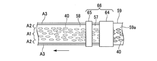
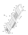
- FIG. 9 is a schematic configuration diagram illustrating an example of a light control member manufacturing apparatus used in the light control member manufacturing method of the present embodiment.
- the manufacturing apparatus 60 shown in FIG. 9 conveys a long base material (first base material) 59 in a roll-to-roll manner and performs various processes during that time.
- a roll-shaped raw fabric roll (mother base material) 55 having a large number of light control member forming regions is formed by the manufacturing apparatus 60.
- a plurality of light control members can be obtained by separating the original roll 55.
- the manufacturing apparatus 60 is provided with a feed roller 61 for feeding the base material 59 at one end, and a winding roller 62 for winding the base material 59 at the other end.
- the base material 59 is configured to move from the delivery roller 61 side toward the take-up roller 62 side.
- a negative photosensitive resin layer forming device 66 composed of a printing device 63, a bar coating device 64 and a first drying device 65, from the delivery roller 61 side toward the take-up roller 62 side, development A device 67, a second drying device 68, and the like are sequentially arranged.
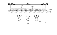
- An exposure device 69 is disposed below the substrate 59.
- the printing device 63 is for printing the light shielding layer 40 made of a black resin on the base material 59.
- the bar coater 64 has a light-sensitive negative photosensitive property on the light shielding layer 40. This is for applying the resin 57.
- the first drying device 65 dries the coated negative photosensitive resin 57 to form the coating film 58. Is.
- the negative type photosensitive resin layer forming device 66 is exemplified by the bar coating device 64 and the first drying device 65.
- the present embodiment is not limited to this.
- a laminating apparatus for laminating the dry film resist on the substrate 59 is used as the negative photosensitive resin layer forming apparatus 66.
- the developing device 67 is for developing the negative photosensitive resin 57 (coating film 58) after exposure with a developer.
- the 2nd drying apparatus 68 is for drying the base material 59 in which the light-diffusion part 41 which consists of the negative photosensitive resin 57 (coating film 58) after development was formed.
- the exposure device 69 is for exposing the coating film 58 of the negative photosensitive resin 57 from the base material 59 side.
- the exposure device 69 includes a plurality of light sources 70.
- the exposure device 69 is disposed on the surface opposite to the one surface 59a of the substrate 59 on which the light shielding layer 40 and the negative photosensitive resin layer 58 are formed.
- the exposure device 69 passes through the base material 59 in a region other than the region where the light shielding layer 40 is formed, and is negatively inclined with respect to the normal direction of the back surface (surface opposite to the surface 59a) of the base material 59 from two directions.
- the negative photosensitive resin layer 58 is exposed by irradiating the type photosensitive resin layer 58 with diffused light composed of ultraviolet light.
- resins such as a thermoplastic polymer, a thermosetting resin, and a photopolymerizable resin are used.
- a thermoplastic polymer such as polyethylene, polypropylene, polyethylene glycol dimethacrylate (PET), polymethyl methacrylate (PMMA), polymethyl methacrylate (PMS), polymethyl methacrylate (PMMA), polymethyl methacrylate (PMS), polymethyl methacrylate (PMMA), polystymer, polystymer, polystymer, polystymer, etc.
- transparent resin made of acrylic polymer, olefin polymer, vinyl polymer, cellulose polymer, amide polymer, fluorine polymer, urethane polymer, silicone polymer, imide polymer, etc.
- a substrate can be used.
- the substrate 59 examples include triacetyl cellulose (TAC) film, polyethylene terephthalate (PET) film, cycloolefin polymer (COP) film, polycarbonate (PC) film, polyethylene naphthalate (PEN) film, polyethersulfone (A substrate made of a transparent resin such as a PES film or a polyimide (PI) film is preferably used.
- TAC triacetyl cellulose
- PET polyethylene terephthalate
- COP cycloolefin polymer
- PC polycarbonate
- PEN polyethylene naphthalate
- PI polyimide
- the base material 59 is a base for applying the material of the light shielding layer 40 and the light diffusion portion 41, and has heat resistance and mechanical strength in a heat treatment step during the manufacturing process. However, it is preferable that the thickness of the base material 59 is thin enough not to impair the heat resistance and mechanical strength. Further, the total light transmittance of the substrate 59 is preferably 90% or more in accordance with JIS K7361-1. When the total light transmittance is 90% or more, sufficient transparency can be obtained.
- the light shielding layer 40 is randomly formed in a predetermined region of the one surface 59a of the base material 59 as shown in FIG.
- the plurality of light shielding layers 40 are regularly formed with the same size, but in actuality, the planar shape is randomly formed in an elongated elliptical shape.
- the light shielding layer 40 is made of, for example, an organic material having light absorption and photosensitivity such as a black resist.
- light shielding is achieved using metal films such as Cr (chromium) and Cr / Cr oxide multilayer films, pigments / dyes used for black ink, and multi-color inks to make black inks.
- Layer 40 may be formed.
- any material having a light shielding property can be used as the material of the light shielding layer 40.
- the thickness of the light shielding layer 40 is set smaller than, for example, the height from the light incident end surface to the light emitting end surface of the light diffusion portion 41.
- FIG. 10 is a flowchart showing a method for manufacturing the light control member.
- 11A to 11C and FIGS. 12A to 12D are cross-sectional views for explaining the manufacturing process of the light control member (raw roll) step by step.
- 12A to 12D are cross-sectional views of the base material 39 in the lateral direction.
- the raw roll 55 is mainly formed by a printing device 63, a negative photosensitive resin layer forming device 66, a developing device 67, and a second drying device 68. Manufactured by performing various treatments in this order.
- a large number of light shielding layers 40 are formed in the first region A1 in the center portion in the short direction of one surface 59a of the long base 59 by the printing device 63 (light shielding).
- the interval (pitch) between the adjacent light shielding layers 40 is not regular or periodic, and is formed randomly.
- the light shielding layer 40 is formed only in the first region A1, and not in the second region A2 and the third region A3. Thereafter, the light shielding layer 40 is dried by a drying device 71 (not shown in FIG. 9).
- the light shielding layer 40 was formed using the printing method, it is not restricted to this.
- the light shielding layer 40 can be formed by a photolithography method using a black negative resist. In this case, if a photomask in which the opening pattern and the light shielding pattern are reversed is used, a positive resist having a light absorption property can also be used. Or you may form the light shielding layer 40 directly using a vapor deposition method, the inkjet method, etc. FIG.
- a negative photosensitive resin 57 is applied to one surface 59a of the base material 59 so as to surround a large number of light shielding layers 40 by the bar coater 64. Specifically, inside the both ends of the base material 39, on the first area A1 where a large number of light shielding layers 40 are formed, and outside the first area A1 (outside along the short direction of the base material 39). It coat
- the negative photosensitive resin 57 for example, an organic material having optical transparency and photosensitivity such as acrylic resin and epoxy resin is used.
- the negative photosensitive resin 57 is preferably one having a refractive index equal to that of the base material 59.
- the negative photosensitive resin layer forming step not only the light shielding layer 40 but also the negative photosensitive resin layer 58 is not formed in the third region A3.
- the negative photosensitive resin 57 is applied using the bar coater 64, but the present invention is not limited to this.
- the negative photosensitive resin 57 may be formed using a slit coater method, a spin coating method, a printing method, or the like.
- the negative photosensitive resin 57 after application is dried by the first drying device 65 to form a coating film (hereinafter referred to as “negative photosensitive resin layer”) 58 (negative photosensitive resin).
- the planar shape is elliptical from the surface opposite to the one surface 59 a of the base material 59 on which the light shielding layer 40 and the negative photosensitive resin layer 58 are formed by the exposure device 69.
- the negative photosensitive resin layer 58 is irradiated with diffused light to expose the negative photosensitive resin layer 58 (negative photosensitive resin layer exposure step: S3).
- the negative photosensitive resin layer 58 is shielded from light by irradiating the negative photosensitive resin layer 58 with diffused light composed of ultraviolet light through the substrate 59 in a region other than the region where the light shielding layer 40 is formed by the exposure device 69.
- the layer 40 is exposed radially so as to spread outward from the non-formation region of the layer 40.
- the negative photosensitive resin layer 58 is developed by the developing device 67 using a dedicated developer (negative photosensitive resin layer developing step: S4). After the development, the negative photosensitive resin layer 58 is cleaned by a cleaning device 72 using a dedicated rinse liquid (pure water or the like). Then, it dries at 80 degreeC with the 2nd drying apparatus 68, and removes the remaining developing solution, rinse solution, and moisture (negative photosensitive resin layer drying process: S5).
- a dedicated developer negative photosensitive resin layer developing step: S4
- a dedicated rinse liquid pure water or the like
- the light diffusion portion 41 having the plurality of hollow portions 42 is formed in the first region A1 of the base material 39, and the support portion 45 is formed in the second region A2.
- the negative photosensitive resin layer 58 is exposed radially so as to spread outward from the region where the light shielding layer 40 is not formed, whereby the forward tapered hollow portion 42 is formed.
- the light diffusion portion 41 has a reverse tapered shape. In the third region A3, a part of the one surface 59a of the base material 59 is exposed.
- the raw roll 55 of the light control member 13 is manufactured.
- the manufactured original fabric roll 55 is once taken up by the take-up roller 62.
- the original fabric roll 55 unwound from the winding roller 62 is cut into a predetermined size according to the liquid crystal panel, and the light control member 13 is separated into pieces (individualization step: S6).
- the raw fabric roll 55 is cut for each light control member forming region A (FIG. 11C) to obtain a plurality of light control members 13 corresponding to the size of the liquid crystal display device to be described later.
- the light control member 13 is completed through the steps described above.
- the cut-out light control member 13 is then bonded to the second polarizing plate 5 of the liquid crystal display body 8. At this time, the light control member 13 is bonded to the liquid crystal display body 8 with the base material 39 facing the viewing side and the light diffusion portion 41 facing the second polarizing plate 5. At this time, as shown in FIG. 1, the light control member 13 has the first region A1 where the light diffusion portion 41 is formed positioned in the display region R in the liquid crystal display body 8, and the first portion where the support portion 45 is formed. The two areas A2 are provided so as to be located in areas other than the display area R.
- the raw roll 55 that is the base material of the light control member 13 is wound around the winding roller 62 of the manufacturing apparatus 60 during the manufacturing process. Since the light diffusion part 41 formed on the base material 59 has a predetermined film thickness, in the case of the conventional configuration (configuration without the support part 45), the base material and the light diffusion part are provided on both sides in the short direction of the base material. There was a step between. When a substrate with such a step is overlapped with a winding roller and wound up, the load concentrates on the edge portions on both sides in the short direction of the light diffusion portion having a plurality of hollow portions, which becomes the edge portion of the step. End up. That is, if there are fine irregularities due to the light diffusing portion at both ends in the short direction of the substrate, the load is concentrated on this portion and the light diffusing portion is easily deformed.
- the hollow portion 42 is formed up to both sides in the short direction of the light diffusing portion 41, the area for receiving the load becomes narrow, so that a large pressure is applied to the light diffusing portion 41 during winding, There is a risk of causing deformation of the light diffusion portion 41. Further, if the contact area between the light diffusion portion 41 and the base material 59 is small in the outer peripheral portion of the light diffusion portion 41, when a force is applied to the peripheral portion of the light diffusion portion 41, the light diffusion portion 41 extends from the base material 59. May peel off.
- the hollow part 42 is not formed in the edge part of the transversal direction both sides of the light-diffusion part 41.
- FIG. In terms of the formation area of the light diffusion portion 41 on the base material 39, the formation area of the support portion 45 per unit area in the second region A2 is larger than the formation area of the light diffusion portion 41 per unit area in the first region A1. Is bigger. That is, the width of the light diffusion portion 41 in the second region A2 is wider than the arrangement interval of the light shielding layers 40 in the first region A1.
- the area for receiving the load is increased, a large pressure is not applied to the light diffusion portion 41 even when the substrate 59 is wound around the winding roller 62. Since the load is dispersed in the support portions 45 provided on both sides of the light diffusion portion 41, the edge portion of the light diffusion portion 41 is prevented from being deformed. Thereby, it becomes the light control member 13 which has the outstanding optical characteristic (light diffusibility). Further, in the outer peripheral portion of the light diffusing portion 41, the adhesion area between the light diffusing portion 41 and the base material 59 is widened, and the adhesion with the base material 59 in the peripheral portion of the light diffusing portion 41 is increased, thereby preventing peeling. Is done.
- FIG. 13 is a plan view showing a schematic configuration of a light control member in the second embodiment.
- a second region A2 is set on the base material 39 so as to surround the first region A1.
- the plurality of light shielding layers 40 are formed only in the first region A1, and are not formed in the second region A2. Therefore, the hollow part 42 formed corresponding to the light shielding layer 40 also exists only in the first region A1, and does not exist in the second region A2.
- the support part 45 formed in the second area A2 is formed integrally with the light diffusion part 41 in the first area A1.
- the light diffusing portion 41 is formed on the inner side than the end portions on both sides in the short side direction of the base material 39 and partially exposes one surface 39 a of the base material 39.
- the support portion 45 does not have the hollow portion 42 and has a certain thickness on the base material 39.
- FIG. 14A to FIG. 14C are plan views for explaining the manufacturing process of the raw fabric roll step by step.
- FIG. 15 is a diagram illustrating a plane of the base material in the manufacturing process of the raw fabric roll.
- a plurality of light-shielding layers are formed in each first region A ⁇ b> 1 on the one surface 39 a of the base material 39 and set at predetermined intervals in the transport direction of the base material 59 by the printing device 63. 40 is formed.
- a space between the first region A1 and the first region A1 is a second region where the light shielding layer 40 is not formed, and the periphery of the first region A1 is surrounded by the second region A2.
- a large number of light shielding layers 40 are not formed continuously in the conveying direction of the base material 59, but the light shielding layers 40 are intermittently formed every predetermined number. Accordingly, there is a region where the light shielding layer 40 is not formed in the conveyance direction of the base material 59. Then, the light shielding layer 40 formed in each 1st area
- the negative photosensitive resin 57 is applied to the first region A1 and the second region A2 on one surface 59a of the base material 59 so as to cover the light shielding layer 40 by the bar coater 64. Apply. Also in the present embodiment, the negative photosensitive resin 57 is not applied to the third regions A3 on both ends of the base material 59 in the short direction.
- the negative photosensitive resin 57 after application is dried by the first drying device 65 to form the negative photosensitive resin layer 58. Thereafter, the negative photosensitive resin layer 58 is exposed by the exposure device 69 using the light shielding layer 40 as a mask.
- the negative photosensitive resin layer 58 is cleaned by the cleaning device 72, and then the second drying device 68. Post bake by In this way, the light diffusion part 41 having the plurality of hollow parts 42 is formed for each first region A1.
- the manufactured original fabric roll 55 is wound around a winding roller. Thereafter, the original roll 55 is unwound from the winding roller, and the original roll 55 is cut for each region where the light control member 13 is formed. As shown in FIG. 15, for each light control member forming region A, the base material 59 is cut in the second region A ⁇ b> 2 where the light shielding layer 40 is not formed in the longitudinal direction of the original fabric roll 55. In the present embodiment, the second region A ⁇ b> 2 is divided into two equal parts in the longitudinal direction of the original fabric roll 55, and a plurality of light control members 13 are obtained. The sheet-like light control member 13 is stored in an overlapping manner, and is sequentially bonded to the liquid crystal display.
- the second region A2 where the light shielding layer 40 is not formed is set on the base material 39 so as to surround the first region A1 where the light shielding layer 40 is formed. That is, the support part 45 in which no hollow part 42 exists is provided at the periphery of the light diffusion part 41 having a large number of hollow parts 42.
- the weight of the upper light control member 13 is used even when a plurality of manufactured light control members 13 are stored in a stacked manner. Therefore, it is possible to prevent the light diffusion portion 41 of the lower light control member 13 from being deformed.
- 16A to 16C show the width W1 of the second region A2 (supporting portion 45) in the short side direction (Y direction) of the base 39 of the light control member 13 and the second region A2 in the long side direction (X direction). (Supporting part 45) It is a figure shown about width W2.
- A2 (supporting part 45) width W2 is equal.
- the second region A2 (support portion 45) width W2 may be wider (W1 ⁇ W2) than the width W1 of the second region A2 (support portion 45).
- the second region A2 (support portion 45) width W2 may be narrower than the width W1 of the second region A2 (support portion 45) (W1> W2). .
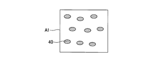
- FIG. 17A is a diagram illustrating the first region A1 where the light shielding layer 40 is provided
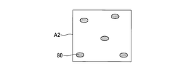
- FIGS. 17B and 17C illustrate a configuration in which the light shielding layer is provided in the second region A2.
- a light shielding layer 80 having a smaller size in plan view than the light shielding layer 40 provided in the first area A1 may be provided in the second area A2.
- the number of light shielding layers 80 provided in a unit area in the second region A2 may be reduced.
- a configuration in which the formation density of the light shielding layers 80 is lower than that in the first region A1 may be employed.
- FIG. 18A is a plan view illustrating a configuration in which a thin light-shielding layer is provided in the second region
- FIG. 18B is a cross-section comparing the thickness of the light-shielding layer in the first region and the light-shielding layer in the second region.
- the thickness T2 of the light shielding layer 81 provided in the second region A2 is set smaller than the thickness T1 of the light shielding layer 40 in the first region A1.
- region A2 a configuration in which a plurality of oval-shaped light-shielding layers in plan view is provided in the second region A2 is illustrated. However, as shown in FIG. You may provide in the whole area
- FIG. 19A is a plan view illustrating a schematic configuration of a light control member according to the third embodiment.
- FIG. 19B is a plan view showing the light control member after cutting out the third region.
- the light control member 53 (light control member 7) in this embodiment includes a first region A1 in which the light shielding layer 40 and the light diffusion portion 41 are formed on one surface 39a of the base material 39, and the first region A1.
- the second region A2 in which the support portion 45 is formed so as to surround the periphery of the first region A1, and the one surface 39a is partially exposed along the two adjacent sides of the base material 39 outside the second region A2.
- a third region A3 to be made.
- the third region A3 may be cut off as necessary.
- FIG. 20A, FIG. 20B, and FIG. 21 are diagrams for explaining a manufacturing process of the light control member in the third embodiment.
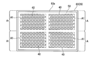
- a large transparent base material 83 having a plurality (four in this case) of light control member formation regions A on one surface 83a is prepared.
- a plurality of light shielding layers 40 are formed in each of the first regions A1 set on the one surface 83a. Adjacent first regions A1 are provided at a predetermined interval from each other, and a second region A2 exists around each of the first regions A1.
- a negative photosensitive resin layer 58 is formed on one surface 83a of the transparent substrate 83 so as to cover all the light shielding layers 40 formed in the first regions A1. At this time, the negative photosensitive resin layer 58 is formed so as to expose the peripheral portion of the one surface 83a which is the third region A3.
- a plurality of light diffusion portions and hollow portions are formed in the first region A1.
- the transparent base material 83 is cut for each light control member forming region A.
- a plurality of light control members 53 are obtained by cutting the second region A2 existing between the adjacent first regions A1 at a position that bisects the second region A2.
- the support portion 45 as a support structure can be formed around the first region A1 having a fine structure. it can. This prevents the light diffusing portion 41 from being deformed due to a load being concentrated on the outer peripheral portion of the light control member 53 located below when the light control members 53 separated into individual pieces are stacked up and down. Can do.
- the transparent base material 83 when the transparent base material 83 is cut during manufacturing, a strong mechanical external force is applied to the cut portion, but the light shielding layer 40 is not formed at the cut portion. For this reason, the adhesive strength between the resin layer (supporting part 45) and the transparent base material 83 is high, and peeling of the resin layer (supporting part 45) from the transparent base material 83 can be suppressed.
- the light control member according to the fourth embodiment will be described below.
- symbol is attached
- the light control member of this embodiment is a light control member with a buffer layer.
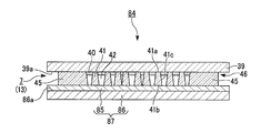
- FIG. 22 is a cross-sectional view illustrating a schematic configuration of a light control member according to the fourth embodiment.
- the light control member 84 (light control member 7) includes a buffer layer (elastic member) 85 and a transparent base material (second base material) on the side opposite to the base material 39 of the light diffusion layer 46. 86, and a buffer base material 87 comprising the same.
- the buffer layer 85 relieves pressure applied around the light control member 84 while elastically deforming when pressure is applied from the base material 39 side.
- the buffer layer 85 is bonded to the light incident end surface 41 b of the light diffusion portion 41.
- the buffer layer 85 for example, an acrylic transparent resin, a polyolefin elastomer, a silicone resin, a urethane resin, rubber, or the like can be used. Among them, it is preferable to use a material having a function (tackiness) as an adhesive layer (pressure-sensitive adhesive). Thereby, the buffer base material 87 can be bonded to the light diffusion layer 46 by the bonding function of the buffer layer 85.
- the buffer layer 85 preferably has a refractive index lower than that of the light diffusion portion 41. In this case, since the reflectance at each interface becomes lower when the refractive index changes stepwise than when the refractive index changes suddenly, the light use efficiency in the light control member 84 can be increased.
- the buffer layer 85 may have optical transparency to ultraviolet light (UV light).
- UV light ultraviolet light
- the negative photosensitive resin layer that becomes the light diffusing portion 41 is irradiated with ultraviolet light (UV light) from the substrate 39 side, and exposure is performed using the light shielding layer 40 as a mask.
- UV light ultraviolet light
- the light diffusing portion 41 can be fully cured (post-cured) without unevenness.
- the transparent substrate 86 has a higher compression elastic modulus than the compression elastic modulus of the buffer layer 85.
- the buffer layer 85 is formed on the entire surface 86 a of the transparent substrate 86.
- the buffer layer 85 is elastically deformed to relieve the force. Thereby, it becomes possible to prevent the deformation of the light diffusion portion 41 more reliably.
- the light control member of the fifth embodiment will be described below.
- symbol is attached
- a light control member having a plurality of light shielding layers, a light diffusion portion, and a hollow portion surrounded by the light diffusion portion in the first region of the substrate.
- the light diffusing portion is configured to be integrally formed so as to fill between the plurality of light shielding layers.
- it has a some light-diffusion part in the 1st area
- FIG. 23 is a longitudinal sectional view of a light control member in the fifth embodiment.
- the light control member 90 (light control member 7) includes a base material 39, a plurality of light diffusion portions 91 provided in the first region A1 on one surface 39a of the base material 39, and a light diffusion portion.
- the light shielding layer 92 is formed so as to cover the one surface 39a around 91, and the support portion 45 is formed in the second region A2. Also in this embodiment, nothing is provided in the third region A3 at least on both ends in the lateral direction of the base material 39, and the one surface 39a is partially exposed.
- the plurality of light diffusion portions 91 have a circular horizontal cross section (xy cross section), the area of the light emission end face 91a on the base 39 side is small, and the area of the light incident end face 91b on the side opposite to the base 39 is large. Is formed.
- Such a light diffusing portion 91 has a so-called reverse-tapered truncated cone shape when viewed from the base material 39 side.
- the light control member 90 is disposed on the liquid crystal display body 8 in such a posture that the side on which the plurality of light diffusing portions 91 are provided faces the second polarizing plate 5 and the base 39 side faces the viewing side. .
- FIG. 24 is a schematic configuration diagram illustrating an example of a light control member manufacturing apparatus.
- the manufacturing apparatus 95 shown in FIG. 24 conveys the long base material 59 by roll-to-roll, and performs various processes in the meantime.
- the manufacturing apparatus 95 includes a feeding roller 61, a winding roller 62, a printing device 63, a first drying device 65, a bar coating device 64, which are arranged from the sending roller 61 side toward the winding roller 62 side. , A developing device 67 and a second drying device 68.
- an exposure device 69 is provided below the substrate 39.
- a polyethylene terephthalate substrate 59 having a thickness of 100 ⁇ m is prepared, and the light shielding layer 92 having a plurality of circular openings 92A is prepared.
- the first surface 59a is formed in the first region A1.
- the circular opening 92A corresponds to the formation region of the light diffusion portion 91 in the next process.
- a transparent negative resist made of an acrylic resin is applied as a light diffusing portion material from the bar coating device 64 so as to cover the light shielding layer 92 from the first region A1 to the second region A2 on the base material 59.
- a coating film 58 having a thickness of 25 ⁇ m is formed.
- the coating film 58 is irradiated with diffused light LF from the base material 59 side using the light shielding layer 92 as a mask to perform exposure.
- the negative photosensitive resin layer 58 is developed by the developing device 67 using a dedicated developer, and is dried at 80 ° C. by the second drying device 68, so that the plurality of light diffusion portions 41 are formed on the substrate 59. Formed on one surface 59a.
- an original fabric roll 96 having a plurality of light control member forming regions is formed, and the light control member 90 according to the present embodiment is completed by dividing the roll 96 into individual light control member forming regions. .
- the support portion 45 having no fine structure in the second region A2 outside the first region A1 in which a large number of frustoconical light diffusion portions 41 are provided and have a fine structure.
- the load applied to both sides of the base material 59 in the short direction can be received by the support portion 45. Thereby, it can prevent that the light-diffusion part 91 deform
- the upper part is a plan view showing a light shielding layer having a rectangular planar shape
- the lower part is a cross-sectional view taken along the line AA of the plan view.
- a light shielding layer 48 having a rectangular planar shape may be used.
- the light shielding layer 48 has a long side direction substantially along the X direction and a short side direction substantially along the Y direction. From this, when considering the direction of the reflection surface 41c of the light diffusion portion 41, the ratio of the reflection surface 41c along the X direction out of the reflection surface 41c of the light diffusion portion 41 is the proportion of the reflection surface 41c along the Y direction. More than.
- the light Ly reflected by the reflecting surface 41c along the X direction and diffused in the Y direction is larger than the light Lx reflected by the reflecting surface 41c along the Y direction and diffused in the X direction. Therefore, the azimuthal direction Vs where the light control member has the strongest diffusibility is the Y direction, which is the minor axis direction of the light shielding layer 48.
- a scattering layer may be added on the viewing side with respect to the second polarizing plate 5 of the liquid crystal display device 1.
- the scattering layer is preferably one that enables isotropic scattering, whereby a smoother luminance visual characteristic (scattering characteristic) can be realized.
- the present invention can be used for a mother substrate, a light control member, a method for manufacturing a light control member, and a display device.
- SYMBOLS 1 Liquid crystal display device (display apparatus), 7 ... Light control member, 8 ... Liquid crystal display body (display body), A ... Light control member formation area, R ... Display area, P ... Disposition space
Landscapes
- Physics & Mathematics (AREA)
- General Physics & Mathematics (AREA)
- Optics & Photonics (AREA)
- Nonlinear Science (AREA)
- Mathematical Physics (AREA)
- Crystallography & Structural Chemistry (AREA)
- Chemical & Material Sciences (AREA)
- Engineering & Computer Science (AREA)
- Manufacturing & Machinery (AREA)
- Health & Medical Sciences (AREA)
- Toxicology (AREA)
- Optical Elements Other Than Lenses (AREA)
- Liquid Crystal (AREA)
- Devices For Indicating Variable Information By Combining Individual Elements (AREA)
Abstract
Priority Applications (2)
| Application Number | Priority Date | Filing Date | Title |
|---|---|---|---|
| JP2015546696A JPWO2015068802A1 (ja) | 2013-11-08 | 2014-11-07 | マザー基材、光制御部材、光制御部材の製造方法、表示装置 |
| US15/033,684 US10036837B2 (en) | 2013-11-08 | 2014-11-07 | Mother substrate, light-control member, method for manufacturing light-control member, and display device |
Applications Claiming Priority (2)
| Application Number | Priority Date | Filing Date | Title |
|---|---|---|---|
| JP2013-232418 | 2013-11-08 | ||
| JP2013232418 | 2013-11-08 |
Publications (1)
| Publication Number | Publication Date |
|---|---|
| WO2015068802A1 true WO2015068802A1 (fr) | 2015-05-14 |
Family
ID=53041577
Family Applications (1)
| Application Number | Title | Priority Date | Filing Date |
|---|---|---|---|
| PCT/JP2014/079581 Ceased WO2015068802A1 (fr) | 2013-11-08 | 2014-11-07 | Substrat mère, élément de commande de lumière, procédé de fabrication d'un élément de commande de lumière, et dispositif d'affichage |
Country Status (3)
| Country | Link |
|---|---|
| US (1) | US10036837B2 (fr) |
| JP (1) | JPWO2015068802A1 (fr) |
| WO (1) | WO2015068802A1 (fr) |
Cited By (3)
| Publication number | Priority date | Publication date | Assignee | Title |
|---|---|---|---|---|
| CN106950745A (zh) * | 2016-01-06 | 2017-07-14 | 三星显示有限公司 | 显示装置 |
| JP2021167915A (ja) * | 2020-04-13 | 2021-10-21 | 浜松ホトニクス株式会社 | 光学素子の製造方法、及び、光学素子 |
| TWI859841B (zh) * | 2022-09-07 | 2024-10-21 | 大陸商南京瀚宇彩欣科技有限責任公司 | 多層導光膜、其製作方法及顯示裝置 |
Families Citing this family (3)
| Publication number | Priority date | Publication date | Assignee | Title |
|---|---|---|---|---|
| CN104820309B (zh) * | 2015-05-19 | 2018-04-17 | 京东方科技集团股份有限公司 | 一种光学组件及其制造方法、偏光片 |
| KR102618811B1 (ko) * | 2017-01-23 | 2023-12-28 | 삼성디스플레이 주식회사 | 색변환 패널 및 이를 포함하는 표시 장치 |
| KR102925199B1 (ko) * | 2020-06-30 | 2026-02-10 | 엘지이노텍 주식회사 | 광 경로 제어 부재 및 이를 포함하는 디스플레이 장치 |
Citations (5)
| Publication number | Priority date | Publication date | Assignee | Title |
|---|---|---|---|---|
| JP2002309199A (ja) * | 2001-04-16 | 2002-10-23 | Sharp Corp | 粘接着シート、積層シート及び液晶表示装置 |
| JP2009222903A (ja) * | 2008-03-14 | 2009-10-01 | Nec Lcd Technologies Ltd | 光学素子アレイシート、表示装置、及びこれらの製造方法 |
| JP2010223996A (ja) * | 2009-03-19 | 2010-10-07 | Mitsubishi Electric Corp | 視野角制御光学シートおよびそれを用いた表示装置 |
| WO2012086424A1 (fr) * | 2010-12-24 | 2012-06-28 | シャープ株式会社 | Elément de diffusion de la lumière, procédé pour sa fabrication et dispositif d'affichage |
| WO2013099839A1 (fr) * | 2011-12-27 | 2013-07-04 | シャープ株式会社 | Dispositif d'affichage à cristaux liquides, film de commande de lumière et dispositif d'affichage |
Family Cites Families (3)
| Publication number | Priority date | Publication date | Assignee | Title |
|---|---|---|---|---|
| JP3702328B2 (ja) | 1999-06-11 | 2005-10-05 | 大日本印刷株式会社 | 光拡散シート |
| JPWO2011062024A1 (ja) * | 2009-11-20 | 2013-04-04 | シャープ株式会社 | 光学部材、照明装置、表示装置、テレビ受信装置、及び光学部材の製造方法 |
| WO2011162013A1 (fr) * | 2010-06-23 | 2011-12-29 | シャープ株式会社 | Dispositif d'affichage et procédé de fabrication de celui-ci |
-
2014
- 2014-11-07 JP JP2015546696A patent/JPWO2015068802A1/ja active Pending
- 2014-11-07 WO PCT/JP2014/079581 patent/WO2015068802A1/fr not_active Ceased
- 2014-11-07 US US15/033,684 patent/US10036837B2/en active Active
Patent Citations (5)
| Publication number | Priority date | Publication date | Assignee | Title |
|---|---|---|---|---|
| JP2002309199A (ja) * | 2001-04-16 | 2002-10-23 | Sharp Corp | 粘接着シート、積層シート及び液晶表示装置 |
| JP2009222903A (ja) * | 2008-03-14 | 2009-10-01 | Nec Lcd Technologies Ltd | 光学素子アレイシート、表示装置、及びこれらの製造方法 |
| JP2010223996A (ja) * | 2009-03-19 | 2010-10-07 | Mitsubishi Electric Corp | 視野角制御光学シートおよびそれを用いた表示装置 |
| WO2012086424A1 (fr) * | 2010-12-24 | 2012-06-28 | シャープ株式会社 | Elément de diffusion de la lumière, procédé pour sa fabrication et dispositif d'affichage |
| WO2013099839A1 (fr) * | 2011-12-27 | 2013-07-04 | シャープ株式会社 | Dispositif d'affichage à cristaux liquides, film de commande de lumière et dispositif d'affichage |
Cited By (5)
| Publication number | Priority date | Publication date | Assignee | Title |
|---|---|---|---|---|
| CN106950745A (zh) * | 2016-01-06 | 2017-07-14 | 三星显示有限公司 | 显示装置 |
| JP2021167915A (ja) * | 2020-04-13 | 2021-10-21 | 浜松ホトニクス株式会社 | 光学素子の製造方法、及び、光学素子 |
| JP7469946B2 (ja) | 2020-04-13 | 2024-04-17 | 浜松ホトニクス株式会社 | 光学素子の製造方法、及び、光学素子 |
| US12099296B2 (en) | 2020-04-13 | 2024-09-24 | Hamamatsu Photonics K.K. | Method for producing optical element and optical element |
| TWI859841B (zh) * | 2022-09-07 | 2024-10-21 | 大陸商南京瀚宇彩欣科技有限責任公司 | 多層導光膜、其製作方法及顯示裝置 |
Also Published As
| Publication number | Publication date |
|---|---|
| US10036837B2 (en) | 2018-07-31 |
| US20160291218A1 (en) | 2016-10-06 |
| JPWO2015068802A1 (ja) | 2017-03-09 |
Similar Documents
| Publication | Publication Date | Title |
|---|---|---|
| US9274255B2 (en) | Light-diffusion member, manufacturing method thereof, and display device | |
| US9846326B2 (en) | Light diffusion member, method for manufacturing same, and display device | |
| US10288781B2 (en) | Display device and light-diffusing member | |
| US9557597B2 (en) | Liquid crystal display device, light control film, and display device | |
| JP6078904B2 (ja) | 光拡散部材、光拡散部材の製造方法、及び表示装置 | |
| US10168569B2 (en) | Display device, adhesive-layer-including light-diffusion member, and method of manufacturing the light-diffusion member | |
| WO2015068802A1 (fr) | Substrat mère, élément de commande de lumière, procédé de fabrication d'un élément de commande de lumière, et dispositif d'affichage | |
| US9279919B2 (en) | Light diffusing member comprising hollow portions and a plurality of light-shielding layers dotted on one surface of a base material, method for manufacturing the same and display device | |
| US10185171B2 (en) | Light control member, method of manufacturing light control member, apparatus for manufacturing light control member, and display device | |
| WO2012157517A1 (fr) | Élément de diffusion lumineuse ainsi que procédé de fabrication de celui-ci, et dispositif d'affichage | |
| US9594194B2 (en) | Light diffusion member, light diffusion member with polarizing plate, and method for fabrication of light diffusion member with polarizing plate | |
| US20160370512A1 (en) | Light diffusing member and display device | |
| US9453946B2 (en) | Light-diffusing member having polarizing plate, production method for light-diffusing member having polarizing plate, and display device | |
| JP2014106249A (ja) | 偏光子およびその製造方法、表示装置 | |
| US10338426B2 (en) | Light diffusion member, base material for light diffusion member production, display device using same and method for producing light diffusion member | |
| WO2015045838A1 (fr) | Elément de dispersion de lumière, dispositif d'affichage et procédé de production d'élément de dispersion de lumière | |
| WO2015037651A1 (fr) | Élément diffusant de la lumière et dispositif d'affichage | |
| JP2014092662A (ja) | 表示装置および表示装置の製造方法 | |
| JP2015094776A (ja) | 光拡散部材および表示装置 | |
| WO2015064493A1 (fr) | Film de régulation lumineuse, rouleau de film de régulation lumineuse et dispositif d'affichage | |
| JP2015090485A (ja) | 光制御フィルムの製造装置、フィルム材、光制御フィルムの製造方法および表示装置 |
Legal Events
| Date | Code | Title | Description |
|---|---|---|---|
| 121 | Ep: the epo has been informed by wipo that ep was designated in this application |
Ref document number: 14859368 Country of ref document: EP Kind code of ref document: A1 |
|
| WWE | Wipo information: entry into national phase |
Ref document number: 15033684 Country of ref document: US |
|
| ENP | Entry into the national phase |
Ref document number: 2015546696 Country of ref document: JP Kind code of ref document: A |
|
| NENP | Non-entry into the national phase |
Ref country code: DE |
|
| 122 | Ep: pct application non-entry in european phase |
Ref document number: 14859368 Country of ref document: EP Kind code of ref document: A1 |