WO2015072417A1 - スイッチング基板 - Google Patents
スイッチング基板 Download PDFInfo
- Publication number
- WO2015072417A1 WO2015072417A1 PCT/JP2014/079691 JP2014079691W WO2015072417A1 WO 2015072417 A1 WO2015072417 A1 WO 2015072417A1 JP 2014079691 W JP2014079691 W JP 2014079691W WO 2015072417 A1 WO2015072417 A1 WO 2015072417A1
- Authority
- WO
- WIPO (PCT)
- Prior art keywords
- bus bar
- control circuit
- disposed
- semiconductor switching
- output bus
- Prior art date
- Legal status (The legal status is an assumption and is not a legal conclusion. Google has not performed a legal analysis and makes no representation as to the accuracy of the status listed.)
- Ceased
Links
Images



Classifications
-
- B—PERFORMING OPERATIONS; TRANSPORTING
- B60—VEHICLES IN GENERAL
- B60L—PROPULSION OF ELECTRICALLY-PROPELLED VEHICLES; SUPPLYING ELECTRIC POWER FOR AUXILIARY EQUIPMENT OF ELECTRICALLY-PROPELLED VEHICLES; ELECTRODYNAMIC BRAKE SYSTEMS FOR VEHICLES IN GENERAL; MAGNETIC SUSPENSION OR LEVITATION FOR VEHICLES; MONITORING OPERATING VARIABLES OF ELECTRICALLY-PROPELLED VEHICLES; ELECTRIC SAFETY DEVICES FOR ELECTRICALLY-PROPELLED VEHICLES
- B60L58/00—Methods or circuit arrangements for monitoring or controlling batteries or fuel cells, specially adapted for electric vehicles
- B60L58/10—Methods or circuit arrangements for monitoring or controlling batteries or fuel cells, specially adapted for electric vehicles for monitoring or controlling batteries
-
- H—ELECTRICITY
- H03—ELECTRONIC CIRCUITRY
- H03K—PULSE TECHNIQUE
- H03K17/00—Electronic switching or gating, i.e. not by contact-making and –breaking
- H03K17/10—Modifications for increasing the maximum permissible switched voltage
- H03K17/102—Modifications for increasing the maximum permissible switched voltage in field-effect transistor switches
-
- H—ELECTRICITY
- H03—ELECTRONIC CIRCUITRY
- H03K—PULSE TECHNIQUE
- H03K17/00—Electronic switching or gating, i.e. not by contact-making and –breaking
- H03K17/12—Modifications for increasing the maximum permissible switched current
- H03K17/122—Modifications for increasing the maximum permissible switched current in field-effect transistor switches
-
- Y—GENERAL TAGGING OF NEW TECHNOLOGICAL DEVELOPMENTS; GENERAL TAGGING OF CROSS-SECTIONAL TECHNOLOGIES SPANNING OVER SEVERAL SECTIONS OF THE IPC; TECHNICAL SUBJECTS COVERED BY FORMER USPC CROSS-REFERENCE ART COLLECTIONS [XRACs] AND DIGESTS
- Y02—TECHNOLOGIES OR APPLICATIONS FOR MITIGATION OR ADAPTATION AGAINST CLIMATE CHANGE
- Y02T—CLIMATE CHANGE MITIGATION TECHNOLOGIES RELATED TO TRANSPORTATION
- Y02T10/00—Road transport of goods or passengers
- Y02T10/60—Other road transportation technologies with climate change mitigation effect
- Y02T10/70—Energy storage systems for electromobility, e.g. batteries
Definitions
- the present invention relates to a switching substrate.
- a substrate having a mechanical relay corresponding to a large current has been conventionally used, but replacement of the mechanical relay with a semiconductor switching element has been proposed for the purpose of miniaturization, long life, and noise reduction.
- a semiconductor switching element it is assumed that a power semiconductor such as a MOSFET (Metal-Oxide-Semiconductor-Field-Effect-Transistor) is used (see Patent Document 1).
- the present invention has been completed based on the above situation, and provides a switching board having a simple configuration arranged between a main power supply and an auxiliary power supply in a vehicle including a main power supply and an auxiliary power supply.
- the purpose is to do.
- the present invention provides a switching board disposed between the main power source and the auxiliary power source in a vehicle including a main power source and an auxiliary power source, and has a first surface and a second surface and is made of an insulating material.
- a control circuit board comprising: an insulating plate, a conductor circuit disposed on the first surface of the insulating plate, and a plurality of mounting windows penetrating from the first surface to the second surface of the insulating plate;
- a circuit structure including an input bus bar and an output bus bar disposed on the second surface of the insulating plate at a distance from each other; and a plurality of circuit structures mounted on the circuit structure and including a drain terminal, a source terminal, and a gate terminal.
- a semiconductor switching element wherein the conductor circuit includes a control circuit and a connection circuit disposed between the input bus bar and the output bus bar, and a part of the plurality of mounting windows includes: ,on the inside The first mounting window in which a part of the input bus bar is exposed, and the other mounting window is a second mounting window in which a part of the output bus bar is exposed, and a part of the plurality of semiconductor switching elements
- the semiconductor switching element is disposed inside the first mounting window, the drain terminal is connected to a part of the input bus bar, the source terminal is connected to the connection circuit, and the gate terminal is connected to the control circuit.
- the first semiconductor switching element to be connected the other semiconductor switching element is disposed inside the second mounting window, the drain terminal is connected to a part of the output bus bar, and the source terminal is the connection circuit
- the switching substrate is a second semiconductor switching element connected to the control circuit and having the gate terminal connected to the control circuit.
- a bus bar, a control circuit substrate, and a semiconductor switching element necessary for the switching substrate disposed between the main power supply and the auxiliary power supply can be simply laid out, and a simple configuration switching substrate is provided. it can.
- the input bus bar is disposed at an edge on the output bus bar side between a plurality of first convex portions projecting toward the output bus bar and two adjacent first convex portions
- the output bus bar is A first recess recessed on the opposite side
- the output bus bar has, on the input bus bar side edge, a plurality of second protrusions protruding toward the input bus bar, and two adjacent second protrusions And a second recess recessed on the opposite side of the input bus bar.
- control circuit board can be prevented from being broken along the gap between the input bus bar and the output bus bar when an unexpectedly large force is applied to the switching board.
- a switching device having a simple configuration that is arranged between the main power source and the auxiliary power source.
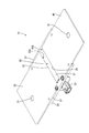
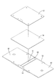
- the perspective view of the switching device of an embodiment The exploded perspective view of the switching device of an embodiment
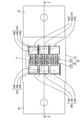
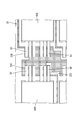
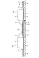
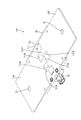
- the perspective view which looked at the switching board of an embodiment from the bus-bar side Top view of switching substrate of embodiment Enlarged view in region R of FIG. AA line sectional view of FIG. Enlarged view in region S of FIG.
- the figure which shows an example of the manufacturing method of the circuit structure of embodiment The perspective view which looked at the switching board of a modification from the bus-bar side
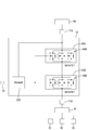
- the switching device 1 is a vehicle including a main battery 90 (corresponding to a main power source) and an auxiliary battery 91 (corresponding to an auxiliary power source), and supplies power from the main battery 90 and the auxiliary battery 91 to the electrical component 92. Is switched. As shown in FIG. 8, the main battery 90 and the auxiliary battery 91 are arranged in series and supply electric power to the electrical component 92. Switching device 1 is arranged in series with respect to main battery 90 and auxiliary battery 91 between main battery 90 and auxiliary battery 91.
- the switching device 1 includes a switching board 10 and a casing 80 that houses the switching board 10.
- the switching substrate 10 includes a circuit configuration body 11 and six semiconductor switching elements 60A and 60B mounted on the circuit configuration body 11.
- the circuit structure 11 includes a control circuit board 20, and two bus bars 30 and 40 and a separator 50 that overlap the control circuit board 20 via an adhesive layer 53.
- the control circuit board 20 has an insulating plate 21 having a first surface and a second surface and made of a glass substrate or a glass nonwoven fabric substrate.
- the control circuit board 20 is a printed board provided with a conductor circuit 22 made of a conductive material on the first surface side of the insulating plate 21.
- a connector 23 for connecting the control circuit board 20 to an external control device (not shown) is disposed at one end of the control circuit board 20.
- the control circuit board 20 has six mounting windows 24A and 24B for mounting the semiconductor switching elements 60A and 60B.
- the mounting windows 24A and 24B are rectangular openings penetrating from the first surface (surface on which the conductor circuit 22 is disposed) of the control circuit board 20 to the second surface (surface opposite to the first surface). The size of the opening is slightly larger than the outer shape of the semiconductor switching elements 60A and 60B.
- three mounting windows (first mounting windows 24A) constitute a set of first mounting window groups 25A arranged in a row.
- the remaining three mounting windows (second mounting windows 24B) constitute a set of second mounting window groups 25B in a line.
- the two sets of mounting window groups 25A and 25B are arranged in parallel with a space between each other.
- the conductor circuit 22 includes a control circuit 22B and a connection circuit 22A.
- the control circuit 22B has a predetermined pattern, one end of which is arranged in the vicinity of each mounting window 24A, 24B, and the other end is connected to a terminal provided in the connector 23, although not shown in detail.
- the connection circuit 22A is disposed on the control circuit board 20 in a region between the two sets of mounting window groups 25A and 25B with a space from the control circuit 22B.
- the input bus bar 30 is a rectangular thick plate made of a conductive material (copper or copper alloy in this embodiment).
- the input bus bar 30 includes a bolt insertion hole 31.
- the bolt insertion hole 31 is a through-hole penetrating from one plate surface of the input bus bar 30 to the other plate surface.
- the output bus bar 40 is a rectangular thick plate formed of a conductive material (copper or copper alloy in this embodiment), and includes a bolt insertion hole 41.
- the input bus bar 30 and the output bus bar 40 are arranged on the second surface of the control circuit board 20.
- the input bus bar 30 and the output bus bar 40 are arranged so that the end faces 32A and 42A facing each other are parallel to each other at an interval. That is, a groove 26 defined by the end surface 32A of the input bus bar 30, the end surface 42A of the output bus bar 40, and the second surface of the insulating plate 21 exists between the input bus bar 30 and the output bus bar 40. .
- the input bus bar 30 and the output bus bar 40 partially overlap the control circuit board 20, and the area where the bolt insertion holes 31 and 41 are arranged is out of the control circuit board 20.
- a part of the input bus bar 30 is exposed inside each first mounting window 24A.
- a part of the output bus bar 40 is exposed inside each second mounting window 24B.
- the separator 50 is disposed on the same surface of the control circuit board 20 as the surface on which the input bus bar 30 and the output bus bar 40 are disposed.
- the separating plate 50 includes a separating portion 51 disposed inside the groove 26 and two frame portions 52 respectively disposed at both ends of the separating portion 51.
- the isolation part 51 is an elongated rectangular plate and is disposed between the input bus bar 30 and the output bus bar 40.
- the two frame portions 52 are portions extending perpendicularly to the separator plate 50 from both ends of the separator plate 50, and are disposed with the input bus bar 30 and the output bus bar 40 interposed therebetween.
- a method of forming the circuit structure 11 configured as described above is, for example, as follows (see FIG. 9). First, the bus bars 30 and 40, the separator plate 50, and the insulating plate 21 are overlapped with the prepreg 54 that is the base material of the adhesive layer 53 interposed therebetween. Next, the bus bars 30 and 40, the separator 50, the insulating plate 21, and the laminate of the prepreg 54 are hot pressed to cure the prepreg 54 and bond the bus bars 30 and 40, the separator 50 and the insulating plate 21. The resin constituting the prepreg 54 flows by hot pressing, and a part of the resin enters the gap between the separator 50 and the input bus bar 30 and the gap between the separator 50 and the output bus bar 40 and is cured. Thereafter, the insulating plate 21 may be machined with a drill to form the mounting windows 24 ⁇ / b> A and 24 ⁇ / b> B, and the conductor circuit 22 may be formed on the surface of the insulating plate 21.
- the semiconductor switching elements 60A and 60B are power MOSFETs and include a housing 61 and a drain terminal 62, a source terminal 63, and a gate terminal 64 provided in the housing 61.
- the drain terminal 62 is disposed on the lower surface of the housing 61. Further, the source terminal 63 and the gate terminal 64 protrude from the side surface of the housing 61.
- first semiconductor switching element 60A three semiconductor switching elements constitute a set of first element group 65A.
- second semiconductor switching elements 60B the remaining three semiconductor switching elements constitute a set of second element group 65B.
- the first semiconductor switching elements 60A are respectively arranged inside the first mounting window 24A.
- the drain terminal 62 is connected to a part of the input bus bar 30 exposed inside the first mounting window 24A
- the source terminal 63 is connected to the connection circuit 22A on the control circuit board 20
- the gate terminal 64 is connected to the control circuit 22B.
- the second semiconductor switching element 60B is disposed inside the second mounting window 24B.
- the drain terminal 62 is connected to a part of the output bus bar 40 exposed inside the second mounting window 24B
- the source terminal 63 is connected to the connection circuit 22A on the control circuit board 20
- the gate terminal 64 is connected to the control circuit 22B.
- the connection can be made with solder H, for example.
- three semiconductor switching elements 60A and 60B connected in parallel are made into one set, and two sets of semiconductor switching elements 60A and 60B are connected in series.
- the two sets of semiconductor switching elements 60A and 60B are arranged back to back (back to back).
- the reason why the plurality of semiconductor switching elements 60A and 60B are set as one set is to cope with a large current. That is, by connecting a plurality of semiconductor switching elements 60A and 60B in parallel, the total amount of current that can be passed through the power supply circuit can be increased.
- a parasitic diode due to a pn junction is generated between the source and the drain. Therefore, even if the gate is turned off, a current flows through the parasitic diode from the source side to the drain side, so that the signal from the source side to the drain side cannot be turned off. For this reason, when the voltage of the auxiliary battery 91 becomes higher than that of the main battery 90 (when idling is stopped, for example), the current flows from the auxiliary battery 91 through the parasitic diode even though the switch is off. It may flow into the battery 90. By connecting two sets of MOSFETs in series so that the directions of the parasitic diodes are opposite to each other, bidirectional current can be cut off.
- the input bus bar 30 has a fastening terminal 71A connected to a harness 70A connected to the main battery 90, a power terminal 72A (stud bolt) inserted through the bolt insertion hole 31, and a nut tightened at the tip of the power terminal 72A. 73A.
- a fastening terminal 71B connected to a harness 70B connected to the auxiliary battery 91 is fastened to the output bus bar 40 at a power terminal 72B (stud bolt) inserted into the bolt insertion hole 41 and the tip of the power terminal 72B. It is fixed with a nut 73B.
- the casing 80 includes a case 81 and a cover plate 82.
- the case 81 is a tray-like case having an outer shape that is slightly larger than the outer shape of the switching substrate 10.
- the case 81 covers the entire surface of the switching substrate 10 on which the control circuit board 20 is disposed.
- the cover plate 82 is a rectangular plate having an outer shape equal to the outer shape of the control circuit board 20.
- the cover plate 82 is overlaid on the switching substrate 10 on the back side of the region where the control circuit board 20 is disposed. Both the case 81 and the cover plate 82 are made of synthetic resin.
- the bus bars 30, 40, the control circuit board 20, and the semiconductor switching elements 60A, 60B necessary for the switching board 10 arranged between the main battery 90 and the auxiliary battery 91 are simply laid out.
- the switching substrate 10 having a simple configuration can be provided.
- the input bus bar 110 has a first convex portion 111A and a first concave portion 111B
- the output bus bar 120 has a second convex portion 121A and a second concave portion 121B. Except for this, the configuration is the same as in the embodiment.
- the same components as those of the embodiment are denoted by the same reference numerals and description thereof is omitted.
- the input bus bar 110 has a plurality of first convex portions 111A that protrude toward the output bus bar 120 at the edge 111 on the output bus bar 120 side.
- the plurality of first convex portions 111A are provided at a constant pitch.
- a region between two adjacent first protrusions 111 ⁇ / b> A and 111 ⁇ / b> A is a first recess 111 ⁇ / b> B that is recessed on the opposite side to the output bus bar 120.
- the output bus bar 120 has a plurality of second convex portions 121 ⁇ / b> A protruding toward the input bus bar 110 at the edge 121 on the input bus bar 110 side.
- the plurality of second convex portions 121A are provided at a constant pitch.
- a region between two adjacent second convex portions 121 ⁇ / b> A and 121 ⁇ / b> A is a second concave portion 121 ⁇ / b> B that is recessed on the opposite side to the input bus bar 110.
- the plurality of first protrusions 111A and the plurality of second protrusions 121A are alternately arranged.
- Each of the plurality of first convex portions 111A is disposed to face the second concave portion 121B, and the protruding end is located in the second concave portion 121B.
- Each of the plurality of second convex portions 121A is disposed to face the first concave portion 111B, and the protruding end is located in the first concave portion 111B.
- control circuit board 20 it is possible to avoid the control circuit board 20 from being broken along the gap between the input bus bar 110 and the output bus bar 120 when an unexpected large force is applied to the switching board 101.
- the auxiliary power source is the auxiliary battery 91.
- a power storage device such as a secondary battery or an electric double layer capacitor can be used.
- the mounting windows 24A and 24B and the semiconductor switching elements 60A and 60B are one set, but the number of semiconductor switching elements constituting one set is two or four or more. It doesn't matter. Similarly, the number of mounting windows constituting one set may be two or four or more.
- Switching board 11 Circuit structure 20: Control circuit board 21: Insulating board 22: Conductor circuit 22A: Control circuit 22B: Connection circuit 24A: 1st mounting window 24B: 2nd mounting window 30, 110: Input bus bar 40, 120: output bus bar 60A: first semiconductor switching element 60B: second semiconductor switching element 62: drain terminal 63: source terminal 64: gate terminal 90: main battery (main power supply) 91: Sub battery (auxiliary power supply) 111: edge 111A: first protrusion 111B: first recess 121: edge 121A: second protrusion 121B: second recess
Landscapes
- Engineering & Computer Science (AREA)
- Life Sciences & Earth Sciences (AREA)
- Sustainable Development (AREA)
- Sustainable Energy (AREA)
- Power Engineering (AREA)
- Transportation (AREA)
- Mechanical Engineering (AREA)
- Connection Or Junction Boxes (AREA)
- Electronic Switches (AREA)
- Inverter Devices (AREA)
- Charge And Discharge Circuits For Batteries Or The Like (AREA)
Abstract
スイッチング基板10は、制御回路22Bと接続回路22Aと第1実装窓24Aと第2実装窓24Bとを第1面に備える制御回路基板20と、制御回路基板20の第2面に配置される入力バスバー30および出力バスバー40を備える回路構成体11と、第1半導体スイッチング素子60Aおよび第2半導体スイッチング素子60Bとを備え、第1半導体スイッチング素子60Aは、第1実装窓24Aの内側に配置され、ドレイン端子62が入力バスバー30に、ソース端子63が接続回路22Aに、ゲート端子64が制御回路22Bにそれぞれ接続され、第2半導体スイッチング素子60Bは、第2実装窓24Bの内側に配置され、ドレイン端子62が出力バスバー40に、ソース端子63が接続回路22Aに、ゲート端子64が制御回路22Bにそれぞれ接続される。
Description
本発明は、スイッチング基板に関する。
近年、燃費向上や環境への配慮のため、メインバッテリの他に補助電源を搭載した自動車が開発されている。例えば、ブレーキ時の回生エネルギーを補助電源に蓄積しておき、走行時に電装品への電力供給に用いることで、オルタネータによる発電量を減らして燃費を向上させることができる。また、アイドリングストップの後のエンジン再始動時に、スタータに補助電源から電力供給することで、メインバッテリの電圧の瞬間的な降下による電装品の瞬断やメインバッテリの劣化を防ぐことができる。
メインバッテリと補助電源との間には、走行やアイドリングストップなどの車両の動作状態に対応して、電力の供給形態を切り替える機能を有するスイッチング基板が設置される場合がある。
スイッチング基板として、従来、大電流に対応したメカニカルリレーを備える基板が用いられてきたが、小型化、高寿命化、静音化を目的として、メカニカルリレーの半導体スイッチング素子への置き換えが提案されている。半導体スイッチング素子としては、MOSFET(金属酸化膜型電界効果トランジスタ;Metal-Oxide-Semiconductor Field-Effect Transistor)などのパワー半導体を使用することが想定される(特許文献1参照)。
ところで、一般に、MOSFETを用いたスイッチでは、pn接合による寄生ダイオードがソース-ドレイン間に生成される。したがって、ゲートをオフしてもソース側からドレイン側へこの寄生ダイオードを通じて電流が流れるため、ソース側からドレイン側への電流の流れを完全に遮断することができない。そこで、双方向の電流を遮断可能にするために、2つのMOSFETを、上記寄生ダイオードの向きが反対になるように直列に接続することがある。
しかし、このような複雑な回路を設計しようとすると、スイッチング基板の構造が複雑となりがちであった。
本発明は上記のような事情に基づいて完成されたものであって、主電源と補助電源とを備える車両において、主電源と補助電源との間に配される簡易な構成のスイッチング基板を提供することを目的とする。
本発明は、主電源と補助電源とを備える車両において、前記主電源と前記補助電源との間に配置されるスイッチング基板であって、第1面及び第2面を有して絶縁性材料からなる絶縁板と、前記絶縁板の前記第1面に配される導体回路と、前記絶縁板の前記第1面から前記第2面まで貫通する複数の実装窓とを備える制御回路基板と、前記絶縁板の前記第2面に互いに間隔を空けて配置される入力バスバーおよび出力バスバーと、を備える回路構成体と、前記回路構成体に実装され、ドレイン端子、ソース端子およびゲート端子を備える複数の半導体スイッチング素子と、を備え、前記導体回路が、制御回路と、前記入力バスバーと前記出力バスバーとの間に配置される接続回路とを備え、前記複数の実装窓のうち一部の実装窓は、内側に前記入力バスバーの一部が露出する第1実装窓であり、他の実装窓は、内側に前記出力バスバーの一部が露出する第2実装窓であり、前記複数の半導体スイッチング素子のうち一部の半導体スイッチング素子は、前記第1実装窓の内側に配置され、前記ドレイン端子が前記入力バスバーの一部に接続され、前記ソース端子が前記接続回路に接続され、前記ゲート端子が前記制御回路に接続される第1半導体スイッチング素子であり、他の半導体スイッチング素子は、前記第2実装窓の内側に配置され、前記ドレイン端子が前記出力バスバーの一部に接続され、前記ソース端子が前記接続回路に接続され、前記ゲート端子が前記制御回路に接続される第2半導体スイッチング素子である、スイッチング基板である。
上記の構成によれば、主電源と補電源との間に配されるスイッチング基板に必要なバスバーや制御回路基板、半導体スイッチング素子をシンプルにレイアウトすることができ、簡易な構成のスイッチング基板を提供できる。
本発明の実施態様としては以下の態様が好ましい。
前記入力バスバーは、前記出力バスバー側の端縁に、前記出力バスバーに向かって突出する複数の第1凸部と、隣り合う2つの前記第1凸部の間に配置され、前記出力バスバーとは逆側に凹む第1凹部とを備え、前記出力バスバーは、前記入力バスバー側の端縁に、前記入力バスバーに向かって突出する複数の第2凸部と、隣り合う2つの前記第2凸部の間に配置され、前記入力バスバーとは逆側に凹む第2凹部とを備えていてもよい。
上記の態様によれば、スイッチング基板に予期しない大きな力が加えられた場合に、入力バスバーと出力バスバーとの隙間に沿って制御回路基板が折れてしまうことを回避できる。
本発明によれば、主電源と補助電源とを備える車両において、主電源と補助電源との間に配される簡易な構成のスイッチング装置を提供できる。
本発明の実施形態を、図1~図9を参照しつつ説明する。
本実施形態のスイッチング装置1は、メインバッテリ90(主電源に該当)と補助バッテリ91(補助電源に該当)とを備える車両において、メインバッテリ90および補助バッテリ91からの電装品92への電力供給の切り替えを行うものである。図8に示すように、メインバッテリ90と補助バッテリ91とは直列に配され、電装品92に電力を供給する。スイッチング装置1は、メインバッテリ90と補助バッテリ91との間に、メインバッテリ90および補助バッテリ91に対して直列に配置されている。
本実施形態のスイッチング装置1は、メインバッテリ90(主電源に該当)と補助バッテリ91(補助電源に該当)とを備える車両において、メインバッテリ90および補助バッテリ91からの電装品92への電力供給の切り替えを行うものである。図8に示すように、メインバッテリ90と補助バッテリ91とは直列に配され、電装品92に電力を供給する。スイッチング装置1は、メインバッテリ90と補助バッテリ91との間に、メインバッテリ90および補助バッテリ91に対して直列に配置されている。
図1および図2に示すように、スイッチング装置1は、スイッチング基板10と、このスイッチング基板10を収容するケーシング80とを備える。スイッチング基板10は、回路構成体11と、この回路構成体11に搭載される6つの半導体スイッチング素子60A、60Bとを備える。回路構成体11は、制御回路基板20と、この制御回路基板20に接着層53を介して重なる2枚のバスバー30、40および隔離板50とを備えている。
制御回路基板20は、第1面及び第2面を有してガラス基材またはガラス不織布基材からなる絶縁板21を有する。制御回路基板20は、前記絶縁板21の第1面側に、導電性材料からなる導体回路22を備えるプリント基板である。制御回路基板20の一端部には、制御回路基板20を外部の制御装置(図示せず)と接続するためのコネクタ23が配置されている。
図4に示すように、制御回路基板20は、半導体スイッチング素子60A、60Bの搭載のための6つの実装窓24A、24Bを有している。実装窓24A、24Bは、制御回路基板20の第1面(導体回路22が配されている面)から、第2面(第1面と逆側の面)まで貫通する矩形の開口部であって、その開口の大きさは、半導体スイッチング素子60A、60Bの外形よりも一回り大きい。6つの実装窓24A、24Bのうち3つの実装窓(第1実装窓24A)は、1列に並んで一組の第1実装窓群25Aを構成している。6つの実装窓24A、24Bのうち残り3つの実装窓(第2実装窓24B)は、1列に並んで一組の第2実装窓群25Bを構成している。二組の実装窓群25A、25Bは、互いに間隔を空けて、並列して配置されている。
導体回路22は、制御回路22Bと接続回路22Aとで構成される。制御回路22Bは、所定のパターンを有しており、その一端は各実装窓24A、24Bの近傍に配置され、他端は、詳細に図示しないが、コネクタ23に備えられる端子に接続されている。接続回路22Aは、制御回路基板20上において、二組の実装窓群25A、25Bの間の領域に、制御回路22Bに対して間隔を空けて配置されている。
2枚のバスバー30、40のうち1枚は入力バスバー30であり、もう1枚は出力バスバー40である。図3に示すように、入力バスバー30は、導電性材料(本実施形態では銅または銅合金)により形成された矩形の厚板である。入力バスバー30は、ボルト挿通孔31を備えている。ボルト挿通孔31は、入力バスバー30の一方の板面から他方の板面まで貫通する貫通孔である。出力バスバー40も、入力バスバー30と同様に、導電性材料(本実施形態では銅または銅合金)により形成された矩形の厚板であって、ボルト挿通孔41を備えている。
入力バスバー30と出力バスバー40とは、制御回路基板20において第2面に配置されている。入力バスバー30と出力バスバー40とは、互いに間隔を空けて、互いに相手側と対向する端面32A、42Aが平行になるように配置されている。つまり、入力バスバー30と出力バスバー40との間には、入力バスバー30の端面32Aと、出力バスバー40の端面42Aと、絶縁板21の第2面とで定義される溝26が存在している。
入力バスバー30および出力バスバー40は、一部の領域が制御回路基板20と重なっており、ボルト挿通孔31、41が配置された領域は制御回路基板20から外れている。各第1実装窓24Aの内側には、入力バスバー30の一部が露出している。各第2実装窓24Bの内側には、出力バスバー40の一部が露出している。
隔離板50は、制御回路基板20において、入力バスバー30および出力バスバー40が配置された面と同じ面に配置されている。隔離板50は、溝26の内部に配置される隔離部51と、隔離部51の両端にそれぞれ配置される2つのフレーム部52とを備えている。隔離部51は、細長い長方形の板であり、入力バスバー30と出力バスバー40との間に配置されている。2つのフレーム部52は、隔離板50の両端から、隔離板50と垂直に延びる部分であって、入力バスバー30および出力バスバー40を挟んで配置されている。
上記のように構成された回路構成体11を形成する方法は、例えば以下のようである(図9参照)。
まず、バスバー30、40および隔離板50と絶縁板21とを、接着層53の基材であるプリプレグ54を挟んで重ねる。次に、バスバー30、40および隔離板50と絶縁板21とプリプレグ54との積層体を熱プレスし、プリプレグ54を硬化させてバスバー30、40および隔離板50と絶縁板21とを接着する。なお、プリプレグ54を構成する樹脂は、熱プレスによって流動し、その一部が隔離板50と入力バスバー30との隙間、および、隔離板50と出力バスバー40との隙間に入り込んで硬化する。この後、絶縁板21にドリルによる機械加工を施して実装窓24A、24Bを形成し、絶縁板21の表面に導体回路22を形成すればよい。
まず、バスバー30、40および隔離板50と絶縁板21とを、接着層53の基材であるプリプレグ54を挟んで重ねる。次に、バスバー30、40および隔離板50と絶縁板21とプリプレグ54との積層体を熱プレスし、プリプレグ54を硬化させてバスバー30、40および隔離板50と絶縁板21とを接着する。なお、プリプレグ54を構成する樹脂は、熱プレスによって流動し、その一部が隔離板50と入力バスバー30との隙間、および、隔離板50と出力バスバー40との隙間に入り込んで硬化する。この後、絶縁板21にドリルによる機械加工を施して実装窓24A、24Bを形成し、絶縁板21の表面に導体回路22を形成すればよい。
半導体スイッチング素子60A、60Bは、パワーMOSFETであって、ハウジング61と、このハウジング61に設けられたドレイン端子62、ソース端子63およびゲート端子64を備えている。ドレイン端子62はハウジング61の下面に配置されている。また、ソース端子63およびゲート端子64は、ハウジング61の側面から突出している。
6つの半導体スイッチング素子60A、60Bのうち3つの半導体スイッチング素子(第1半導体スイッチング素子60A)は、一組の第1素子群65Aを構成している。6つの半導体スイッチング素子60A、60Bのうち残り3つの半導体スイッチング素子(第2半導体スイッチング素子60B)は、一組の第2素子群65Bを構成している。
図4に示すように、第1半導体スイッチング素子60Aは、それぞれ、第1実装窓24Aの内側に配置されている。そして、第1実装窓24Aの内側に露出している入力バスバー30の一部にドレイン端子62が接続され、制御回路基板20上の接続回路22Aにソース端子63が、制御回路22Bにゲート端子64が、それぞれ接続されている。同様に、第2半導体スイッチング素子60Bは、それぞれ、第2実装窓24Bの内側に配置されている。そして、第2実装窓24Bの内側に露出している出力バスバー40の一部にドレイン端子62が接続され、制御回路基板20上の接続回路22Aにソース端子63が、制御回路22Bにゲート端子64がそれぞれ接続されている。接続は、例えばはんだHにより行うことができる。
このように配置されることによって、並列に接続された3つの半導体スイッチング素子60A、60Bが1組とされ、2組の半導体スイッチング素子60A、60Bが直列に接続される。2組の半導体スイッチング素子60A、60Bは、互いに背中合わせ(back to back)に配置されている。
複数の半導体スイッチング素子60A、60Bを1組とするのは、大電流に対応するためである。つまり、複数の半導体スイッチング素子60A、60Bを並列に接続することによって、電源回路に流すことのできる電流の総量を大きくできる。
2組の半導体スイッチング素子60A、60Bを背中合わせに配置するのは、以下の理由による。
一般に、MOSFETを用いたスイッチでは、pn接合による寄生ダイオードがソース-ドレイン間に生成される。したがって、ゲートをオフしてもソース側からドレイン側へこの寄生ダイオードを通じて電流が流れるため、ソース側からドレイン側への信号をオフすることができない。このため、メインバッテリ90よりも補助バッテリ91の電圧が高くなった時(アイドリングストップ時など)に、スイッチがオフになっているにもかかわらず、寄生ダイオードを通って電流が補助バッテリ91からメインバッテリ90に流れ込んでしまうことがある。2組のMOSFETを、上記寄生ダイオードの向きが反対になるように直列に接続することによって、双方向の電流を遮断することが可能となる。
入力バスバー30には、メインバッテリ90につながるハーネス70Aと接続された締結端子71Aが、ボルト挿通孔31に挿通された電源端子72A(スタッドボルト)と、この電源端子72Aの先端に締め付けられたナット73Aとによって固定される。また、出力バスバー40には、補助バッテリ91につながるハーネス70Bと接続された締結端子71Bが、ボルト挿通孔41に挿通された電源端子72B(スタッドボルト)と、この電源端子72Bの先端に締め付けられたナット73Bとによって固定される。
ケーシング80は、ケース81と覆い板82とを備えている。ケース81は、スイッチング基板10の外形よりも一回り大きい外形を有するトレイ状のケースである。ケース81は、スイッチング基板10の制御回路基板20が配置された面を全面にわたって覆っている。覆い板82は、制御回路基板20の外形と等しい外形を有する矩形状の板である。覆い板82は、スイッチング基板10において、制御回路基板20が配置された領域の裏側に重ねられている。ケース81と覆い板82とはいずれも合成樹脂により形成されている。
(本実施形態の効果)
本実施形態によれば、メインバッテリ90と補助バッテリ91との間に配されるスイッチング基板10に必要なバスバー30、40、制御回路基板20、および半導体スイッチング素子60A、60Bをシンプルにレイアウトすることができ、簡易な構成のスイッチング基板10を提供できる。
本実施形態によれば、メインバッテリ90と補助バッテリ91との間に配されるスイッチング基板10に必要なバスバー30、40、制御回路基板20、および半導体スイッチング素子60A、60Bをシンプルにレイアウトすることができ、簡易な構成のスイッチング基板10を提供できる。
<変形例>
本発明の変形例を、図10を参照しつつ説明する。本変形例のスイッチング基板101は、入力バスバー110が第1凸部111Aと第1凹部111Bとを有し、出力バスバー120が第2凸部121Aと第2凹部121Bとを有している点を除き、実施形態と同様の構成である。スイッチング基板101において、実施形態と同様の構成については、同一の符号を付して説明を省略する。
本発明の変形例を、図10を参照しつつ説明する。本変形例のスイッチング基板101は、入力バスバー110が第1凸部111Aと第1凹部111Bとを有し、出力バスバー120が第2凸部121Aと第2凹部121Bとを有している点を除き、実施形態と同様の構成である。スイッチング基板101において、実施形態と同様の構成については、同一の符号を付して説明を省略する。
入力バスバー110は、出力バスバー120側の端縁111に、出力バスバー120に向かって突出する複数の第1凸部111Aを有している。複数の第1凸部111Aは、一定のピッチで設けられている。隣り合う2つの第1凸部111A、111A間の領域は、出力バスバー120とは逆側に凹む第1凹部111Bとなっている。
出力バスバー120は、入力バスバー110側の端縁121に、入力バスバー110に向かって突出する複数の第2凸部121Aを有している。複数の第2凸部121Aは、一定のピッチで設けられている。隣り合う2つの第2凸部121A、121A間の領域は、入力バスバー110とは逆側に凹む第2凹部121Bとなっている。
複数の第1凸部111Aと複数の第2凸部121Aとは、互い違いに配置されている。複数の第1凸部111Aのそれぞれは、第2凹部121Bと向い合せに配置され、突出端が第2凹部121B内に位置している。複数の第2凸部121Aのそれぞれは、第1凹部111Bと向い合せに配置され、突出端が第1凹部111B内に位置している。
上記の構成によれば、スイッチング基板101に予期しない大きな力が加えられた場合に、入力バスバー110と出力バスバー120との隙間に沿って制御回路基板20が折れてしまうことを回避できる。
<他の実施形態>
本発明は上記記述及び図面によって説明した実施形態に限定されるものではなく、例えば次のような実施形態も本発明の技術的範囲に含まれる。
(1)上記実施形態では、溝26の内部に隔離板50の隔離部51が配置される例を示したが、例えば、制御回路基板20とバスバー30、40とを接着した後に、溝26に熱硬化性樹脂を流し込んで硬化させることにより、溝26を埋めても構わない。
本発明は上記記述及び図面によって説明した実施形態に限定されるものではなく、例えば次のような実施形態も本発明の技術的範囲に含まれる。
(1)上記実施形態では、溝26の内部に隔離板50の隔離部51が配置される例を示したが、例えば、制御回路基板20とバスバー30、40とを接着した後に、溝26に熱硬化性樹脂を流し込んで硬化させることにより、溝26を埋めても構わない。
(2)上記実施形態では、補助電源は補助バッテリ91であったが、補助電源としては、例えば、二次電池、電気二重層キャパシタなどの蓄電装置を使用できる。
(3)上記実施形態では、実装窓24A、24Bおよび半導体スイッチング素子60A、60Bは3つが1組とされていたが、1組を構成する半導体スイッチング素子の数は2つまたは4つ以上であっても構わない。同様に、1組を構成する実装窓の数は2つまたは4つ以上であっても構わない。
10、101:スイッチング基板
11:回路構成体
20:制御回路基板
21:絶縁板
22:導体回路
22A:制御回路
22B:接続回路
24A:第1実装窓
24B:第2実装窓
30、110:入力バスバー
40、120:出力バスバー
60A:第1半導体スイッチング素子
60B:第2半導体スイッチング素子
62:ドレイン端子
63:ソース端子
64:ゲート端子
90:メインバッテリ(主電源)
91:サブバッテリ(補助電源)
111:端縁
111A:第1凸部
111B:第1凹部
121:端縁
121A:第2凸部
121B:第2凹部
11:回路構成体
20:制御回路基板
21:絶縁板
22:導体回路
22A:制御回路
22B:接続回路
24A:第1実装窓
24B:第2実装窓
30、110:入力バスバー
40、120:出力バスバー
60A:第1半導体スイッチング素子
60B:第2半導体スイッチング素子
62:ドレイン端子
63:ソース端子
64:ゲート端子
90:メインバッテリ(主電源)
91:サブバッテリ(補助電源)
111:端縁
111A:第1凸部
111B:第1凹部
121:端縁
121A:第2凸部
121B:第2凹部
Claims (2)
- 主電源と補助電源とを備える車両において、前記主電源と前記補助電源との間に配置されるスイッチング基板であって、
第1面及び第2面を有して絶縁性材料からなる絶縁板と、前記絶縁板の前記第1面に配される導体回路と、前記絶縁板の前記第1面から前記第2面まで貫通する複数の実装窓とを備える制御回路基板と、前記絶縁板の前記第2面に互いに間隔を空けて配置される入力バスバーおよび出力バスバーと、を備える回路構成体と、
前記回路構成体に実装され、ドレイン端子、ソース端子およびゲート端子を備える複数の半導体スイッチング素子と、を備え、
前記導体回路が、制御回路と、前記入力バスバーと前記出力バスバーとの間に配置される接続回路とを備え、
前記複数の実装窓のうち一部の実装窓は、内側に前記入力バスバーの一部が露出する第1実装窓であり、他の実装窓は、内側に前記出力バスバーの一部が露出する第2実装窓であり、
前記複数の半導体スイッチング素子のうち一部の半導体スイッチング素子は、前記第1実装窓の内側に配置され、前記ドレイン端子が前記入力バスバーの一部に接続され、前記ソース端子が前記接続回路に接続され、前記ゲート端子が前記制御回路に接続される第1半導体スイッチング素子であり、他の半導体スイッチング素子は、前記第2実装窓の内側に配置され、前記ドレイン端子が前記出力バスバーの一部に接続され、前記ソース端子が前記接続回路に接続され、前記ゲート端子が前記制御回路に接続される第2半導体スイッチング素子である、スイッチング基板。 - 前記入力バスバーは、前記出力バスバー側の端縁に、前記出力バスバーに向かって突出する複数の第1凸部と、隣り合う2つの前記第1凸部の間に配置され、前記出力バスバーとは逆側に凹む第1凹部とを備え、
前記出力バスバーは、前記入力バスバー側の端縁に、前記入力バスバーに向かって突出する複数の第2凸部と、隣り合う2つの前記第2凸部の間に配置され、前記入力バスバーとは逆側に凹む第2凹部とを備えている、請求項1に記載のスイッチング基板。
Priority Applications (3)
| Application Number | Priority Date | Filing Date | Title |
|---|---|---|---|
| US15/036,730 US9969291B2 (en) | 2013-11-13 | 2014-11-10 | Switching board |
| EP14862220.2A EP3054596B1 (en) | 2013-11-13 | 2014-11-10 | Switching substrate |
| CN201480060998.2A CN105745841A (zh) | 2013-11-13 | 2014-11-10 | 开关基板 |
Applications Claiming Priority (2)
| Application Number | Priority Date | Filing Date | Title |
|---|---|---|---|
| JP2013-234818 | 2013-11-13 | ||
| JP2013234818A JP6115779B2 (ja) | 2013-11-13 | 2013-11-13 | スイッチング基板 |
Publications (1)
| Publication Number | Publication Date |
|---|---|
| WO2015072417A1 true WO2015072417A1 (ja) | 2015-05-21 |
Family
ID=53057351
Family Applications (1)
| Application Number | Title | Priority Date | Filing Date |
|---|---|---|---|
| PCT/JP2014/079691 Ceased WO2015072417A1 (ja) | 2013-11-13 | 2014-11-10 | スイッチング基板 |
Country Status (5)
| Country | Link |
|---|---|
| US (1) | US9969291B2 (ja) |
| EP (1) | EP3054596B1 (ja) |
| JP (1) | JP6115779B2 (ja) |
| CN (1) | CN105745841A (ja) |
| WO (1) | WO2015072417A1 (ja) |
Families Citing this family (3)
| Publication number | Priority date | Publication date | Assignee | Title |
|---|---|---|---|---|
| JP6252872B2 (ja) * | 2015-02-24 | 2017-12-27 | 株式会社オートネットワーク技術研究所 | 電気接続箱及び接続端子部品 |
| JP2020013895A (ja) * | 2018-07-18 | 2020-01-23 | 株式会社オートネットワーク技術研究所 | 回路基板 |
| JP6958515B2 (ja) * | 2018-09-03 | 2021-11-02 | 株式会社オートネットワーク技術研究所 | 回路構造体及び電気接続箱 |
Citations (7)
| Publication number | Priority date | Publication date | Assignee | Title |
|---|---|---|---|---|
| JPH10126963A (ja) * | 1996-10-14 | 1998-05-15 | Yazaki Corp | 車両用電源分配装置 |
| US20050151508A1 (en) * | 2004-01-14 | 2005-07-14 | Alexander Cook | Battery isolator |
| JP2006060949A (ja) * | 2004-08-23 | 2006-03-02 | Matsushita Electric Ind Co Ltd | 電源バックアップユニットおよびこれを用いた電子制御装置 |
| JP2009017705A (ja) * | 2007-07-05 | 2009-01-22 | Yazaki Corp | 電気接続箱及び電気接続箱の製造方法 |
| JP2009146933A (ja) | 2007-12-11 | 2009-07-02 | Denso Corp | バスバーとバスバーを備えた半導体装置 |
| US20110127830A1 (en) * | 2009-12-01 | 2011-06-02 | John Wayne Harding | Battery Isolator Unit |
| JP2013187488A (ja) * | 2012-03-09 | 2013-09-19 | Panasonic Corp | 半導体リレー装置 |
Family Cites Families (9)
| Publication number | Priority date | Publication date | Assignee | Title |
|---|---|---|---|---|
| DE19813369B4 (de) * | 1998-03-26 | 2006-11-23 | Robert Bosch Gmbh | Vorrichtung zur Spannungsversorgung in einem Kraftfahrzeug |
| JP3927017B2 (ja) | 2001-11-26 | 2007-06-06 | 株式会社オートネットワーク技術研究所 | 回路構成体及びその製造方法 |
| DE10254910B4 (de) * | 2001-11-26 | 2008-12-24 | AutoNetworks Technologies, Ltd., Nagoya | Schaltkreisbildende Einheit und Verfahren zu deren Herstellung |
| US7046535B2 (en) * | 2003-12-17 | 2006-05-16 | Ballard Power Systems Corporation | Architecture for power modules such as power inverters |
| JP2006310557A (ja) | 2005-04-28 | 2006-11-09 | Auto Network Gijutsu Kenkyusho:Kk | スイッチングユニット |
| CN101263547A (zh) * | 2005-06-24 | 2008-09-10 | 国际整流器公司 | 具有低电感的半导体半桥模块 |
| US7928607B2 (en) * | 2007-03-29 | 2011-04-19 | Lamar Technologies Llc | Aircraft power system and apparatus for supplying power to an aircraft electrical system |
| JP5320040B2 (ja) | 2008-11-27 | 2013-10-23 | 株式会社熊谷組 | バイブレータ |
| CN102005810A (zh) * | 2010-11-26 | 2011-04-06 | 刘卉 | 车辆供电系统和方法、电源、安装装置及电源转接装置 |
-
2013
- 2013-11-13 JP JP2013234818A patent/JP6115779B2/ja active Active
-
2014
- 2014-11-10 US US15/036,730 patent/US9969291B2/en active Active
- 2014-11-10 WO PCT/JP2014/079691 patent/WO2015072417A1/ja not_active Ceased
- 2014-11-10 EP EP14862220.2A patent/EP3054596B1/en active Active
- 2014-11-10 CN CN201480060998.2A patent/CN105745841A/zh active Pending
Patent Citations (7)
| Publication number | Priority date | Publication date | Assignee | Title |
|---|---|---|---|---|
| JPH10126963A (ja) * | 1996-10-14 | 1998-05-15 | Yazaki Corp | 車両用電源分配装置 |
| US20050151508A1 (en) * | 2004-01-14 | 2005-07-14 | Alexander Cook | Battery isolator |
| JP2006060949A (ja) * | 2004-08-23 | 2006-03-02 | Matsushita Electric Ind Co Ltd | 電源バックアップユニットおよびこれを用いた電子制御装置 |
| JP2009017705A (ja) * | 2007-07-05 | 2009-01-22 | Yazaki Corp | 電気接続箱及び電気接続箱の製造方法 |
| JP2009146933A (ja) | 2007-12-11 | 2009-07-02 | Denso Corp | バスバーとバスバーを備えた半導体装置 |
| US20110127830A1 (en) * | 2009-12-01 | 2011-06-02 | John Wayne Harding | Battery Isolator Unit |
| JP2013187488A (ja) * | 2012-03-09 | 2013-09-19 | Panasonic Corp | 半導体リレー装置 |
Non-Patent Citations (1)
| Title |
|---|
| See also references of EP3054596A4 * |
Also Published As
| Publication number | Publication date |
|---|---|
| US20160264014A1 (en) | 2016-09-15 |
| JP6115779B2 (ja) | 2017-04-19 |
| EP3054596A4 (en) | 2016-11-16 |
| JP2015095798A (ja) | 2015-05-18 |
| CN105745841A (zh) | 2016-07-06 |
| EP3054596B1 (en) | 2020-03-25 |
| EP3054596A1 (en) | 2016-08-10 |
| US9969291B2 (en) | 2018-05-15 |
Similar Documents
| Publication | Publication Date | Title |
|---|---|---|
| JP6213776B2 (ja) | スイッチング基板 | |
| JP5169353B2 (ja) | パワーモジュール | |
| JP3793407B2 (ja) | 電力変換装置 | |
| JP6222713B2 (ja) | バスバー構造及びバスバー構造を用いた電力変換装置 | |
| CN111095769B (zh) | 电力转换装置 | |
| CN112992845B (zh) | 功率模块及其制造方法 | |
| JP2008004953A (ja) | 半導体モジュール及びそれを用いた電力変換装置 | |
| JP6115779B2 (ja) | スイッチング基板 | |
| JP6136946B2 (ja) | スイッチング基板 | |
| JP4655020B2 (ja) | 平滑コンデンサモジュール及びこれを用いた電力変換装置 | |
| US9960700B2 (en) | Electronic apparatus | |
| JP4055643B2 (ja) | インバータ装置 | |
| JP2009033902A (ja) | パワーモジュール | |
| KR102694820B1 (ko) | 컨버터 | |
| KR102756060B1 (ko) | 전자 부품 조립체 | |
| CN112951818B (zh) | 功率转换装置 | |
| KR102873669B1 (ko) | 인쇄회로기판 모듈 및 이를 포함하는 컨버터 | |
| JP6604406B2 (ja) | 電源装置 | |
| JP2003060143A (ja) | 半導体モジュール | |
| JP2016063554A (ja) | 電源装置 | |
| WO2025032484A1 (en) | Electronic power conversion appliance for electric or hybrid vehicles | |
| JP2015139288A (ja) | スイッチング基板 | |
| KR20210039580A (ko) | 기판 모듈 및 이를 포함하는 컨버터 | |
| KR20150031633A (ko) | 차량용 인버터 | |
| JP2022081768A (ja) | 電力変換装置 |
Legal Events
| Date | Code | Title | Description |
|---|---|---|---|
| 121 | Ep: the epo has been informed by wipo that ep was designated in this application |
Ref document number: 14862220 Country of ref document: EP Kind code of ref document: A1 |
|
| REEP | Request for entry into the european phase |
Ref document number: 2014862220 Country of ref document: EP |
|
| WWE | Wipo information: entry into national phase |
Ref document number: 2014862220 Country of ref document: EP |
|
| NENP | Non-entry into the national phase |
Ref country code: DE |
|
| WWE | Wipo information: entry into national phase |
Ref document number: 15036730 Country of ref document: US |