WO2015076014A1 - パワー半導体モジュールのドライブ制御方式およびパワー半導体モジュールの制御回路 - Google Patents
パワー半導体モジュールのドライブ制御方式およびパワー半導体モジュールの制御回路 Download PDFInfo
- Publication number
- WO2015076014A1 WO2015076014A1 PCT/JP2014/075346 JP2014075346W WO2015076014A1 WO 2015076014 A1 WO2015076014 A1 WO 2015076014A1 JP 2014075346 W JP2014075346 W JP 2014075346W WO 2015076014 A1 WO2015076014 A1 WO 2015076014A1
- Authority
- WO
- WIPO (PCT)
- Prior art keywords
- power semiconductor
- temperature information
- alarm signal
- unit
- semiconductor module
- Prior art date
- Legal status (The legal status is an assumption and is not a legal conclusion. Google has not performed a legal analysis and makes no representation as to the accuracy of the status listed.)
- Ceased
Links
Images
Classifications
-
- H—ELECTRICITY
- H03—ELECTRONIC CIRCUITRY
- H03K—PULSE TECHNIQUE
- H03K17/00—Electronic switching or gating, i.e. not by contact-making and –breaking
- H03K17/08—Modifications for protecting switching circuit against overcurrent or overvoltage
- H03K17/082—Modifications for protecting switching circuit against overcurrent or overvoltage by feedback from the output to the control circuit
-
- H—ELECTRICITY
- H02—GENERATION; CONVERSION OR DISTRIBUTION OF ELECTRIC POWER
- H02H—EMERGENCY PROTECTIVE CIRCUIT ARRANGEMENTS
- H02H3/00—Emergency protective circuit arrangements for automatic disconnection directly responsive to an undesired change from normal electric working condition with or without subsequent reconnection ; integrated protection
- H02H3/16—Emergency protective circuit arrangements for automatic disconnection directly responsive to an undesired change from normal electric working condition with or without subsequent reconnection ; integrated protection responsive to fault current to earth, frame or mass
-
- H—ELECTRICITY
- H03—ELECTRONIC CIRCUITRY
- H03K—PULSE TECHNIQUE
- H03K17/00—Electronic switching or gating, i.e. not by contact-making and –breaking
- H03K17/08—Modifications for protecting switching circuit against overcurrent or overvoltage
- H03K17/082—Modifications for protecting switching circuit against overcurrent or overvoltage by feedback from the output to the control circuit
- H03K17/0828—Modifications for protecting switching circuit against overcurrent or overvoltage by feedback from the output to the control circuit in composite switches
-
- H—ELECTRICITY
- H03—ELECTRONIC CIRCUITRY
- H03K—PULSE TECHNIQUE
- H03K17/00—Electronic switching or gating, i.e. not by contact-making and –breaking
- H03K17/18—Modifications for indicating state of switch
-
- H—ELECTRICITY
- H03—ELECTRONIC CIRCUITRY
- H03K—PULSE TECHNIQUE
- H03K19/00—Logic circuits, i.e. having at least two inputs acting on one output; Inverting circuits
- H03K19/02—Logic circuits, i.e. having at least two inputs acting on one output; Inverting circuits using specified components
- H03K19/173—Logic circuits, i.e. having at least two inputs acting on one output; Inverting circuits using specified components using elementary logic circuits as components
- H03K19/1731—Optimisation thereof
- H03K19/1732—Optimisation thereof by limitation or reduction of the pin/gate ratio
-
- H—ELECTRICITY
- H02—GENERATION; CONVERSION OR DISTRIBUTION OF ELECTRIC POWER
- H02H—EMERGENCY PROTECTIVE CIRCUIT ARRANGEMENTS
- H02H3/00—Emergency protective circuit arrangements for automatic disconnection directly responsive to an undesired change from normal electric working condition with or without subsequent reconnection ; integrated protection
- H02H3/08—Emergency protective circuit arrangements for automatic disconnection directly responsive to an undesired change from normal electric working condition with or without subsequent reconnection ; integrated protection responsive to excess current
-
- H—ELECTRICITY
- H02—GENERATION; CONVERSION OR DISTRIBUTION OF ELECTRIC POWER
- H02H—EMERGENCY PROTECTIVE CIRCUIT ARRANGEMENTS
- H02H9/00—Emergency protective circuit arrangements for limiting excess current or voltage without disconnection
- H02H9/02—Emergency protective circuit arrangements for limiting excess current or voltage without disconnection responsive to excess current
-
- H—ELECTRICITY
- H03—ELECTRONIC CIRCUITRY
- H03K—PULSE TECHNIQUE
- H03K17/00—Electronic switching or gating, i.e. not by contact-making and –breaking
- H03K17/08—Modifications for protecting switching circuit against overcurrent or overvoltage
- H03K2017/0806—Modifications for protecting switching circuit against overcurrent or overvoltage against excessive temperature
Definitions
- the present invention combines the temperature information acquired from the power semiconductor module on the high voltage side and the alarm signal, and transmits the signal to the control unit on the low voltage side through one insulating element such as a photocoupler to
- the present invention relates to a drive control system and a control circuit for a power semiconductor module that reduces the number of insulating elements provided on the side interface.
- IGBT Insulated Gate Bipolar Transistor
- IGBT Insulated Gate Bipolar Transistor with sense function
- FWD wheeling diode
- temperature detection diode for detecting the temperature in the module
- the output current (specifically, the current flowing in the sense region of the IGBT) is detected to detect the presence or absence of a short circuit and prevent the power semiconductor module from being destroyed.
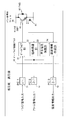
- FIG. 1 is a diagram showing a configuration of a drive control system of a conventional power semiconductor module.
- a gate drive unit 51 provided on the high voltage side applies a predetermined drive voltage to the gate of the IGBT 61 to operate the IGBT and to short-circuit protection unit 52 as a protection unit for coping with an abnormality of a semiconductor module described later.
- the gate drive unit 51 receives a signal output from the undervoltage protection unit 53 to protect the IGBT 61.
- the undervoltage protection unit 53 detects a drop in a DC voltage (not shown) applied to the gate drive unit 51 to compensate for the voltage shortage and protect the gate drive unit 51.
- the short-circuit protection unit 52 operates as described below to protect the gate drive unit 51 and thus protect the power semiconductor module 60.
- the IGBT 61 provided on the high voltage side detects the main current flowing through the IGBT using the sensing function of the IGBT, and continuously detects the overcurrent protection level set for the detected main current for a predetermined period.
- the overcurrent is determined by detecting whether or not the overcurrent has been exceeded, and if it is overcurrent, the switch control of the IGBT 61 by the gate drive unit 51 is interrupted to prevent the IGBT from being destroyed by the overcurrent.
- the short-circuit protection unit 52 when the overcurrent is detected, the short-circuit protection unit 52 generates an alarm signal from the alarm signal output terminal provided on the low voltage side via the photocoupler 72 (PC2) provided between the high voltage side and the low voltage side. (Not shown).
- a latch period is set for the alarm signal, the alarm state is maintained during the latch period, and an action is taken for the alarm before the end of the alarm latch period (for example, release if the alarm can be canceled). Is implemented.
- a temperature detecting element eg, temperature detecting diode
- a substrate semiconductor substrate (chip), printed circuit board, etc.
- the converted temperature information is converted into a digital signal (described later) by the temperature information creation unit 54, and the digitized temperature information is provided on the low pressure side via a photocoupler 73 (PC3) provided between the high pressure side and the low pressure side.
- the temperature information is output from a temperature information output terminal to a control unit (not shown).
- the gate drive control block 50 is comprised by the gate drive part 51, the short circuit protection part 52, the undervoltage protection part 53, and the temperature information preparation part 54, Usually, this gate drive control block 50 is integrated into IC. Has been.
- the control unit (not shown) provided on the low voltage side is constituted by, for example, a central control unit (CPU) or a logic IC, or a system LSI on which the logic IC and the CPU are mounted. (PC2), the alarm signal and the temperature information sent via the photocoupler 73 (PC3) are received, the contents are analyzed, and the drive signal input terminal and photocoupler 71 ( The gate drive unit 51 is instructed via PC1). For example, when the control unit (not shown) determines that the power semiconductor module 60 should be protected from overcurrent by analyzing the alarm state, the IGBT 61 is connected to the gate drive unit 51 via the drive signal input terminal and the photocoupler 71 (PC1). Is instructed to stop the on-off operation of and to fix it off.
- the control unit (not shown) has, for example, described the instruction to reduce the overload in order to reduce the temperature of the power semiconductor module 60.
- the signal is sent to the gate drive unit 51 via the drive signal input terminal and the photocoupler 71 (PC1), and is operated so as to reduce the overload.
- PC1 photocoupler 71
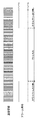
- FIG. 2 is a view showing signal waveforms related to temperature information and an alarm signal in a drive control system of a conventional power semiconductor module.
- the temperature information in the figure is a PWM signal in which the duty ratio of the pulse ON width is determined by the temperature detected by the temperature detection element 63, and is a low voltage from the temperature information creation unit 54 via the photocoupler 73 (PC 3).
- PC 3 photocoupler 73
- the alarm signal in the figure shows a waveform composed of binary states so that it shows a high level state during normal operation without alarm output and a low level state during protection operation with alarm output. 52 to the low-voltage side control unit (not shown) via the photocoupler 72 (PC2).
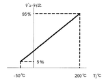
- FIG. 3 is a diagram showing the setting of the duty ratio of the pulse ON width with respect to temperature information in the drive control method of the conventional power semiconductor module.
- the frequency of the PWM signal used for the output of temperature information in Fig. 2 is normally set to several kHz, and the duty ratio of the PWM signal used for the output of temperature information is accurate to express the temperature information. However, since the figure becomes too complicated, the detailed pulse ON width representing the PWM signal is not shown.
- Patent Document 1 is divided into an upper arm and a lower arm, and both arms are provided with switching elements SWU and SWD composed of IGBTs with a sense function.
- Each of the switching elements SWU and SWD is a gate driver with a protection function.
- the alarm output (alarm signal) of SU2 and SD2 and the temperature information output of SU3 and SD3 are passed through the isolation transformers TU2, TD2; TU3, TD3, respectively.
- a signal transmission circuit using an air-core type insulated transformer that is separately transmitted to the control circuit side is disclosed.
- Patent Document 2 discloses an intelligent power module in which insulating elements and terminals are provided as many as the number of signals.
- the alarm signal propagation means 11 is constituted by a photocoupler (insulating element), and the temperature information propagation means 12 is similarly constituted by a photocoupler. Furthermore, it is disclosed that an alarm signal and temperature information are output in parallel from the intelligent power module 1 to the alarm signal propagation means 11 and the temperature information propagation means 12.
- IPM Intelligent Power Module
- Patent Document 1 has a configuration in which the alarm signal and the temperature information are separately insulated and output by two insulating transformers (insulating elements), so the number of insulating elements increases. In addition, there is a problem that the number of terminals at the input / output terminals for enabling reception by the insulating element increases.
- Patent Document 2 uses a photocoupler as an insulating element, and separately outputs an alarm signal and temperature information separately from each other by a separate photocoupler. Therefore, there is a problem that the number of insulating elements increases as in Patent Document 1 and the number of terminals at the input / output terminals for transmitting and receiving signals via the insulating elements also increases.
- the first problem of the present invention is that the temperature information acquired from the power semiconductor module on the high-voltage side and the alarm signal are combined and transmitted to the control unit on the low-voltage side through one insulating element.
- the object is to reduce the number of insulating elements for completely insulating electrically.
- the second problem of the present invention is that the temperature information acquired from the power semiconductor module on the high voltage side and the alarm signal are combined and transmitted to the control unit on the low voltage side through one insulating element.
- the purpose is to reduce the number of terminals for signal transmission to the low voltage side.
- the drive control system for the power semiconductor module includes a drive control unit and a power semiconductor module arranged on the high voltage side, and a control unit for controlling the drive control unit arranged on the high voltage side on the low voltage side.
- the drive control unit applies a predetermined voltage to the gate of the power semiconductor device to control on / off of the power semiconductor device; and
- a temperature information is created by converting a temperature detected by a temperature detecting element arranged on a substrate of the power semiconductor module and a protection unit that copes with the abnormal state and outputs an alarm signal when the abnormal state is detected. Created by the temperature information generator and the alarm signal and temperature information generator.
- a synthesizing unit that synthesizes the inputted alarm signal and temperature information, and the synthesizing unit synthesizes the temperature information acquired from the power semiconductor module and the alarm signal, and The combined output is output to one insulating element provided between the high voltage side and the low voltage side.
- the protection unit includes a short-circuit protection unit that interrupts on / off control of the power semiconductor device by the gate drive unit and outputs an overcurrent alarm signal when an overcurrent of the power semiconductor device is detected, and the alarm The signal is based on the overcurrent alarm signal.
- the protection unit includes an overheat protection unit that performs overheat protection of the power semiconductor device semiconductor module and outputs an overheat alarm signal, and the alarm signal is based on the overheat alarm signal.
- the synthesis unit is configured by an AND circuit that takes a logical product of the temperature information and the alarm signal.
- the synthesis unit synthesizes and outputs the temperature information input by being inserted into the temperature information input / output path, and outputs the temperature information in response to the alarm signal. It consists of a switch that shuts off / passes.
- the switch is connected between the temperature information input / output terminal and the reference potential, and the on / off of the switch is controlled by the alarm signal.
- the switch is composed of an NPN transistor, the collector of the NPN transistor is connected to the temperature information input / output terminal, the emitter is connected to the reference potential, and the base is connected to the output side of the inverting circuit.
- the input side of the inverting circuit is connected to the alarm signal input terminal.
- the switch is composed of a PNP transistor, the emitter of the PNP transistor is connected to the temperature information input / output terminal, the collector is connected to the reference potential, and the base is connected to the alarm signal input terminal. I have to.
- the insulating element is a photocoupler.
- the power semiconductor module control circuit of the present invention is a control circuit that is provided on the high voltage side and controls the power semiconductor module provided on the high voltage side, and applies a predetermined voltage to the gate of the power semiconductor device.
- a gate drive unit that controls on / off of the power semiconductor device; and a short-circuit protection unit that shuts off the on / off control of the power semiconductor device by the gate drive unit and outputs an alarm signal when an overcurrent of the power semiconductor device is detected;
- a temperature information creation unit that creates temperature information by converting a temperature detected by a temperature detection element disposed on the substrate of the power semiconductor module into a digital signal, and a temperature created by the alarm signal and the temperature information creation unit Combining information and synthesizing the input alarm signal and temperature information
- the combining unit combines the temperature information acquired from the power semiconductor module and the alarm signal, and outputs the combined output to one insulating element provided between the high voltage side and the low voltage side. I have to.
- the present invention since the number of insulating elements such as photocouplers necessary for each one-phase IGBT can be reduced by one as compared with the conventional one, the present invention can be applied to a large system such as a three-phase inverter having a six-phase IPM. When applied, the number of insulating elements such as photocouplers can be greatly reduced (six reductions can be achieved with a 6-phase IPM), thereby ensuring advantages in terms of mounting space and cost.
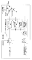
- FIG. 4 is a diagram showing the configuration of the drive control system of the power semiconductor module according to the embodiment of the present invention.
- the power semiconductor module 20 shown in FIG. 4 includes an IGBT (Insulated Gate Bipolar Transistor) (hereinafter simply referred to as IGBT) 21 that is a kind of power semiconductor device, A free wheeling diode (Free Wheeling Diode (hereinafter simply referred to as FWD)) 22 that is connected in parallel to the IGBT and flows a current in the opposite direction to the current flowing in the IGBT, and a temperature detection diode 23 that detects the temperature in the module.
- IGBT, FWD, and temperature detection diode which are components of the power semiconductor module, are formed in one or a plurality of semiconductor chips.
- the temperature detecting diode may be replaced with another temperature detecting element such as a thermistor.
- a gate drive unit 11 provided on the high voltage side applies a predetermined drive voltage to the gate of the IGBT 21 to operate the IGBT 21 and, at the same time, a short-circuit protection unit 12 as a protection unit for coping with an abnormality in a semiconductor module described later.
- the IGBT 21 is protected by receiving a signal output from the undervoltage protection unit 13.
- the undervoltage protection unit 13 protects the gate drive unit 11 by detecting a drop in a DC voltage (not shown) applied to the gate drive unit 11 to compensate for the voltage shortage.
- the short-circuit protection unit 12 operates as described below to protect the gate drive unit 11 and thus protect the power semiconductor module 20.
- the IGBT 21 provided on the high voltage side detects the main current flowing through the IGBT using the sensing function of the IGBT, and whether the detected main current has continuously exceeded the preset overcurrent protection level for a predetermined period.
- the short circuit protection unit 12 detects whether or not the overcurrent is determined. If the overcurrent is detected, the switch control of the IGBT 21 by the gate drive unit 11 is interrupted to prevent the IGBT from being destroyed by the overcurrent. On the other hand, when the short circuit protection unit 12 detects an overcurrent, the short circuit protection unit 12 outputs an alarm signal to the synthesis unit 15.
- a latch period is set for the alarm signal, the alarm state is maintained during the latch period, and an action for the alarm is performed until the end of the alarm latch period (for example, if the alarm can be released, the alarm is released, etc.) ) Is implemented.
- the temperature of the substrate including the power semiconductor module 20 is detected using a temperature detection element (eg, temperature detection diode) 23 provided on a substrate (semiconductor substrate (chip), printed circuit board, or the like) on which the power semiconductor module 20 is mounted,
- the detected temperature is converted into a digital signal (described later) by the temperature information creation unit 14, and the digitized temperature information is output to the synthesis unit 15.
- the synthesizing unit 15 outputs only temperature information during normal operation without alarm output, and synthesizes the output of temperature information and an alarm signal during protection operation with alarm output.
- the low level signal is transmitted to the control unit (not shown) from the temperature information and alarm signal output terminal provided on the low voltage side via the photocoupler 3 (PC3) provided between the high voltage side and the low voltage side. .
- the gate drive control block (control circuit) 10 is comprised by the gate drive part 11, the short circuit protection part 12, the undervoltage protection part 13, the temperature information preparation part 14, and the synthetic
- the control unit (not shown) provided on the low voltage side is constituted by, for example, a central control unit (CPU) or a logic IC, or a system LSI on which the logic IC and the CPU are mounted. Instruct the gate drive unit 11 via the drive signal input terminal and the photocoupler 1 (PC1) to analyze the temperature information and the contents of the alarm signal output obtained via the (PC3) and perform predetermined processing. .
- CPU central control unit
- PC1 photocoupler 1
- control unit determines that the power semiconductor module 20 should be protected from overcurrent by analyzing the alarm signal obtained by the photocoupler 3 (PC3) via the synthesis unit 15, the drive signal input terminal, The gate drive unit 11 is instructed to stop the on / off operation of the IGBT 21 and fix it off via the photocoupler 1 (PC1).
- control unit analyzes the contents of the temperature information output obtained by the photocoupler 3 (PC3) via the synthesis unit 15 and performs a drive signal to perform a process of lowering the temperature of the power semiconductor module 20.
- An instruction is given to the gate drive unit 11 via the input terminal and the photocoupler 1 (PC1).
- an instruction for reducing the overload is sent to the gate drive unit 11 via the drive signal input terminal and the photocoupler 1 (PC1) to reduce the overload.
- the combined output of the temperature information and the alarm signal obtained on the high voltage side is passed through one photocoupler 3 (PC3). Since it is configured to transmit to a control unit (not shown) provided on the low voltage side, the number of photocouplers can be reduced as compared with the conventional configuration (specifically, one for each one-phase IGBT).
- the combined output of the temperature information obtained on the high voltage side and the alarm signal is sent to the low voltage via one photocoupler 3 (PC3). Since the signal is transmitted to a control unit (not shown) provided on the side, the number of terminals for signal transmission between the input and output can be reduced as compared with the conventional configuration. That is, if the number of terminals is reduced, it is possible to reduce the number of terminals with which the other party exchanging signals. Therefore, in general, the apparatus scale can be reduced, and the cost can be reduced accordingly.
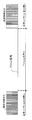
- FIG. 5 is a diagram showing a signal waveform after the combined output of the temperature information and the alarm signal in the drive control method of the power semiconductor module according to the embodiment of the present invention.
- the signal waveform after combined output during normal operation is only the temperature information output
- the signal waveform after combined output during protective operation is output
- an alarm output is output.
- the combined output waveform of temperature information and alarm signal during protection operation is fixed at a low level (a specific example will be described later)
- a PWM (pulse width modulation) signal indicating temperature information output is output.
- the latch period is set for the alarm signal and the low level alarm signal is set to be maintained for a predetermined period
- the low level of the PWM signal indicating the temperature information output, the low level of the alarm signal May be identified by the duration. Therefore, there is no need for a separate signal indicating which the low level is.
- the temperature (analog signal) detected by the temperature detection element 23 in the temperature information creation unit 14 is converted into digital information by pulse width modulation (PWM).
- PWM pulse width modulation
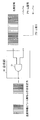
- FIG. 6 is a diagram showing a first example of the synthesis unit according to the embodiment of the present invention shown in FIG.
- the synthesizer 30 includes an AND circuit 31 that takes a logical product of temperature information and an alarm signal. Since the alarm signal is set to a high level during normal operation (no alarm output), the PWM signal indicating the output of temperature information passes through the AND circuit 31 and is output to the output side. That is, since the PWM signal that has passed through the AND circuit 31 is applied to the anode of the light emitting diode of the photocoupler 3 (PC3), this can be detected by a control unit (not shown) on the low voltage side.
- PC3 photocoupler 3
- the PWM signal indicating the output of temperature information is prevented from passing through the AND circuit 31 and the PWM indicating the output of temperature information on the output side. No signal is output.
- the output side of the AND circuit 31 is set to a low level only during the low level period of the alarm signal, and this low level signal is input to the light emitting section of the photocoupler 3 (PC3). Thereby, it can be detected by the low pressure side control unit (not shown) that the presence of alarm is output from the combining unit 30 as a combined output of the temperature information and the alarm signal.
- the alarm signal is set to the high level again after the output side of the AND circuit 31 outputs the low level for the low level period with the alarm.
- the PWM signal indicating the output of the signal passes through the AND circuit 31 and is applied to the anode of the light emitting diode of the photocoupler 3 (PC3).
- PC3 light emitting diode of the photocoupler 3
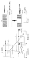
- FIG. 7 is a diagram showing a second example of the synthesis unit according to the embodiment of the present invention shown in FIG.
- the synthesis unit 40 synthesizes and outputs the temperature information inserted into the temperature information input / output path and the alarm signal, and cuts off the input of the temperature information according to the presence or absence of the alarm.
- It is composed of a switch 41 that passes through. When there is an alarm output, the switch 41 is turned ON, and the combined output of the temperature information and the alarm signal at that time is the temperature information during the period when the alarm output is present (the latch period or the period during which the alarm is generated).
- the PWM signal at the temperature information input terminal is not output from the output terminal of the synthesizer 40, and a reference potential (ground, ie, low level) is output.
- a reference potential ground, ie, low level
- (A) shown in the right part of FIG. 7 shows that when the switch 41 is OFF with no alarm output in the above, the PWM signal input from the combining unit 40 to the temperature information input terminal is continued. It shows how it is output to the light emitting section of (PC3).
- (b) shown in the right part of FIG. 7 shows that when the switch 41 is turned on with the alarm output, the combined output of the temperature information and the alarm signal is the temperature information input / output path during the period when the alarm output is present. Since the PWM signal at the temperature information input terminal is not output to the output side (the light emitting unit of the photocoupler 3 (PC3)) because it is fixed at the low level.
- FIG. 7 is a diagram showing a specific example 1 and a specific example 2 of the switches in the synthesis unit 40 described above.
- the collector of the NPN transistor 411 is connected to the temperature information input / output terminal of the synthesis unit 40, the emitter is connected to the reference potential (ground), and the base is connected to the output side of the inverter (inverting circuit) 412.
- the input side of the inverter (inverting circuit) 412 is connected to the alarm input terminal.
- the combined output of the temperature information and the alarm signal in the combining unit 40 is such that the temperature information input / output path is fixed at a low level during the period when the alarm output is present. It is fixed to the reference potential (ground) without being transmitted to (the light emitting portion of the photocoupler 3 (PC3)).
- the output side of the inverter 412 becomes low level, and this low level signal is applied to the base of the NPN transistor 411 and the NPN transistor 411. Becomes non-conductive.
- the combined output of the temperature information and the alarm signal in the combining unit 40 is equal to the PWM signal input to the temperature information input terminal because the temperature information input / output path is not connected to the reference potential, and the PWM signal continues. Then, it is output to the output side (light emitting part of the photocoupler 3 (PC3)).
- the emitter of the PNP transistor 413 is connected to the temperature information input / output terminal of the synthesis unit 40, the collector is connected to the reference potential (ground), and the base is connected to the alarm input terminal.
- the PNP transistor 413 When the alarm output is present (the alarm signal is at low level) and the alarm input terminal is at low level, the PNP transistor 413 is turned on. As a result, the combined output of the temperature information and the alarm signal in the combining unit 40 is such that the temperature information input / output path is fixed at a low level during the period when the alarm output is present. It is fixed to the reference potential (ground) without being transmitted to (the emitting portion of the photocoupler 3 (PC3)). On the other hand, when there is no alarm output (the alarm signal is high level) and the alarm input terminal becomes high level, the PNP transistor 413 becomes non-conductive.
- the combined output of the temperature information and the alarm signal in the combining unit 40 is equal to the PWM signal input to the temperature information input terminal because the temperature information input / output path is not connected to the reference potential, and the PWM signal continues. Then, it is output to the output side (light emitting part of the photocoupler 3 (PC3)).
- the temperature information and the pulse ON width (duty ratio) setting in the drive control method of the power semiconductor module according to the embodiment of the present invention are the temperatures in the drive control method of the power semiconductor module shown in FIG. Since it is the same as the setting of information and pulse ON width (duty ratio), it is not reexplained here.
- a method for digitizing temperature information other methods such as frequency modulation and coding of temperature information can be used in addition to the above. In any case, it is sufficient that the longest period of the low level is shorter than the latch period of the alarm signal.
- the composite output waveform is fixed at a low level during protection operation with alarm output, but the signal is generated by performing frequency modulation, etc., different from the modulation method for transmitting temperature information output to the output side when alarm output is present. Information on the presence of alarm output can be obtained on the receiving side (low pressure side).
- the modulation method is not limited to frequency modulation as long as the modulation method can be received on the low-pressure side.
- two photocouplers that are conventionally required for three one-phase IGBTs can be made two, so a three-phase having a six-phase IPM.
- the short-circuit protection unit that outputs an alarm signal related to a short circuit has been described as an example of the protection unit, the present invention is not limited to this.
- the present invention has an overheat protection unit, and when the overheat protection unit detects overheating of the semiconductor module based on the temperature information, the overheat protection of the semiconductor module is performed on the high pressure side and an alarm signal related to overheating is output.
- the alarm signal according to the present invention may be a single alarm signal combined with an alarm signal caused by other factors such as a short circuit.
- the present invention is not limited to this, and for example, an insulating transformer may be used as the insulating element.
- a multiplexer that selects and outputs either temperature information or a reference potential based on an alarm signal may be applied as the synthesis unit.
- the pulse ON width has been described as a period in which the pulse is at a low level, it may be a period in which the pulse is at a high level.
- the present invention has been described by taking a photocoupler as an example of an insulating element for signal transmission from the high voltage side to the low voltage side, the present invention can also be realized by using another insulating element for signal transmission, such as an isolator IC. Is possible.
Landscapes
- Physics & Mathematics (AREA)
- Engineering & Computer Science (AREA)
- Computer Hardware Design (AREA)
- Computing Systems (AREA)
- General Engineering & Computer Science (AREA)
- Mathematical Physics (AREA)
- Power Conversion In General (AREA)
- Inverter Devices (AREA)
- Electronic Switches (AREA)
Abstract
Description
高圧側に設けられたIGBT21は、当該IGBTのセンス機能を利用してIGBTに流れる主電流の検出を行い、検出した主電流があらかじめ設定してある過電流保護レベルを所定期間連続して超えたか否かを短絡保護部12で検出して過電流を判定し、過電流であればゲートドライブ部11によるIGBT21のスイッチ制御を遮断することで過電流によるIGBTの破壊を防止する。その一方、短絡保護部12は、過電流を検出すると、アラーム信号を合成部15に出力する。通常、アラーム信号にはラッチ期間が設定されていて、ラッチ期間の間はアラーム状態が維持され、アラームラッチ期間の終了までの間にアラームに対する処置(例えばアラーム解除が可能であれば解除を行う等)が実施される。
Claims (10)
- 高圧側にドライブ制御部とパワー半導体モジュールとが配置され、低圧側に前記高圧側に配置された前記ドライブ制御部を制御する制御部とを備えてなるパワー半導体モジュールのドライブ制御方式において、前記ドライブ制御部は、
パワー半導体デバイスのゲートに所定の電圧を印加して該パワー半導体デバイスのオンオフを制御するゲートドライブ部と、
前記パワー半導体デバイスの異常状態に対処するととともに異常状態を検出するとアラーム信号を出力する保護部と、
前記パワー半導体モジュールの基板に配置された温度検出素子で検出された温度をデジタル信号に変換して温度情報を作成する温度情報作成部と、
前記アラーム信号及び前記温度情報作成部で作成された温度情報が入力されて、該入力されたアラーム信号及び温度情報を合成する合成部とを含み、
該合成部は、前記パワー半導体モジュールから取得した温度情報とアラーム信号とを合成し、その合成出力を前記高圧側と前記低圧側の間に設けられる一つの絶縁素子に出力することを特徴とするパワー半導体モジュールのドライブ制御方式。 - 前記保護部は、前記パワー半導体デバイスの過電流を検出すると前記ゲートドライブ部による前記パワー半導体デバイスのオンオフ制御を遮断するとともに過電流アラーム信号を出力する短絡保護部を有し、前記アラーム信号が前記過電流アラーム信号によるものであることを特徴とする請求項1に記載のパワー半導体モジュールのドライブ制御方式。
- 前記保護部は、前記パワー半導体デバイス半導体モジュールの過熱保護を行うとともに過熱アラーム信号を出力する過熱保護部を有し、前記アラーム信号が前記過熱アラーム信号によるものであることを特徴とする請求項1に記載のパワー半導体モジュールのドライブ制御方式。
- 前記合成部は、前記温度情報と前記アラーム信号との論理積をとるアンド回路で構成されることを特徴とする請求項1に記載のパワー半導体モジュールのドライブ制御方式。
- 前記合成部は、前記温度情報の入出力経路に挿入されて入力された前記温度情報と前記アラーム信号とを合成し出力するもので、前記アラーム信号に応じて前記温度情報の入力を遮断/通過させるスイッチで構成されることを特徴とする請求項1に記載のパワー半導体モジュールのドライブ制御方式。
- 前記スイッチは、温度情報入出力端と基準電位との間に接続され、そのオンオフが前記アラーム信号により制御されることを特徴とする請求項5に記載のパワー半導体モジュールのドライブ制御方式。
- 前記スイッチは、NPNトランジスタで構成され、該NPNトランジスタのコレクタが前記温度情報入出力端に接続され、エミッタが前記基準電位に接続され、ベースが反転回路の出力側に接続され、該反転回路の入力側が前記アラーム信号入力端に接続されていることを特徴とする請求項6に記載のパワー半導体モジュールのドライブ制御方式。
- 前記スイッチは、PNPトランジスタで構成され、該PNPトランジスタのエミッタが前記温度情報入出力端に接続され、コレクタが前記基準電位に接続され、ベースが前記アラーム信号入力端に接続されていることを特徴とする請求6に記載のパワー半導体モジュールのドライブ制御方式。
- 前記絶縁素子がフォトカプラであることを特徴とする請求項1ないし8のいずれか1項に記載のドライブ制御方式。
- 高圧側に設けられて、高圧側に設けられたパワー半導体モジュールを制御する制御回路であって、
パワー半導体デバイスのゲートに所定の電圧を印加して該パワー半導体デバイスのオンオフを制御するゲートドライブ部と、
前記パワー半導体デバイスの過電流を検出すると前記ゲートドライブ部による前記パワー半導体デバイスのオンオフ制御を遮断するとともにアラーム信号を出力する短絡保護部と、
前記パワー半導体モジュールの基板に配置された温度検出素子で検出された温度をデジタル信号に変換して温度情報を作成する温度情報作成部と、
前記アラーム信号及び前記温度情報作成部で作成された温度情報が入力されて、該入力されたアラーム信号及び温度情報を合成する合成部とを有し、
該合成部は、前記パワー半導体モジュールから取得した温度情報とアラーム信号とを合成し、その合成出力を前記高圧側と低圧側の間に設けられる一つの絶縁素子に出力することを特徴とするパワー半導体モジュールの制御回路。
Priority Applications (4)
| Application Number | Priority Date | Filing Date | Title |
|---|---|---|---|
| EP14864653.2A EP2996232B1 (en) | 2013-11-22 | 2014-09-25 | Power semiconductor module drive control system and power semiconductor module control circuit |
| CN201480032137.3A CN105264757B (zh) | 2013-11-22 | 2014-09-25 | 功率半导体模块的驱动控制方式以及功率半导体模块的控制电路 |
| JP2015549026A JP6160707B2 (ja) | 2013-11-22 | 2014-09-25 | パワー半導体モジュールのドライブ制御方式およびパワー半導体モジュールの制御回路 |
| US14/985,091 US9768763B2 (en) | 2013-11-22 | 2015-12-30 | Drive control method of power semiconductor module and control circuit of power semiconductor module |
Applications Claiming Priority (2)
| Application Number | Priority Date | Filing Date | Title |
|---|---|---|---|
| JP2013242221 | 2013-11-22 | ||
| JP2013-242221 | 2013-11-22 |
Related Child Applications (1)
| Application Number | Title | Priority Date | Filing Date |
|---|---|---|---|
| US14/985,091 Continuation US9768763B2 (en) | 2013-11-22 | 2015-12-30 | Drive control method of power semiconductor module and control circuit of power semiconductor module |
Publications (1)
| Publication Number | Publication Date |
|---|---|
| WO2015076014A1 true WO2015076014A1 (ja) | 2015-05-28 |
Family
ID=53179285
Family Applications (1)
| Application Number | Title | Priority Date | Filing Date |
|---|---|---|---|
| PCT/JP2014/075346 Ceased WO2015076014A1 (ja) | 2013-11-22 | 2014-09-25 | パワー半導体モジュールのドライブ制御方式およびパワー半導体モジュールの制御回路 |
Country Status (5)
| Country | Link |
|---|---|
| US (1) | US9768763B2 (ja) |
| EP (1) | EP2996232B1 (ja) |
| JP (1) | JP6160707B2 (ja) |
| CN (1) | CN105264757B (ja) |
| WO (1) | WO2015076014A1 (ja) |
Cited By (6)
| Publication number | Priority date | Publication date | Assignee | Title |
|---|---|---|---|---|
| US20170019092A1 (en) * | 2014-09-29 | 2017-01-19 | Fuji Electric Co., Ltd. | Semiconductor device |
| CN108475997A (zh) * | 2015-12-10 | 2018-08-31 | 株式会社电装 | 信号传输电路 |
| JP2019097305A (ja) * | 2017-11-22 | 2019-06-20 | 三菱電機株式会社 | 電力半導体モジュールおよび電力変換装置 |
| JP2019140434A (ja) * | 2018-02-06 | 2019-08-22 | 株式会社デンソー | スイッチの駆動装置 |
| US10651720B2 (en) | 2016-05-25 | 2020-05-12 | Mitsubishi Electric Corporation | Intelligent power module |
| JP2023010666A (ja) * | 2021-07-09 | 2023-01-20 | セミコンダクター・コンポーネンツ・インダストリーズ・リミテッド・ライアビリティ・カンパニー | 温度監視機能を有するゲートドライバ |
Families Citing this family (16)
| Publication number | Priority date | Publication date | Assignee | Title |
|---|---|---|---|---|
| US10191021B2 (en) * | 2015-02-27 | 2019-01-29 | Deere & Company | Method for estimating a temperature of a transistor |
| CN107949986B (zh) * | 2016-03-04 | 2021-05-18 | 富士电机株式会社 | 半导体元件的驱动装置 |
| US10833595B2 (en) | 2016-07-01 | 2020-11-10 | Rohm Co., Ltd. | Semiconductor device with upper and lower switching devices and isolation transformer |
| US9917435B1 (en) * | 2016-09-13 | 2018-03-13 | Ford Global Technologies, Llc | Piecewise temperature compensation for power switching devices |
| CN108666981A (zh) * | 2017-03-28 | 2018-10-16 | 中国科学院上海微系统与信息技术研究所 | 一种igbt过流保护电路及方法 |
| US11316510B1 (en) | 2018-02-16 | 2022-04-26 | Maxim Integrated Products, Inc. | Transistors drivers with fast shutdown-capability, and associated systems and methods |
| CN109493773A (zh) * | 2018-12-11 | 2019-03-19 | 惠科股份有限公司 | 一种显示面板的过电流保护值的设计方法和测试机台 |
| JP7038647B2 (ja) * | 2018-12-12 | 2022-03-18 | 三菱電機株式会社 | インテリジェントパワーモジュール |
| CN109799721B (zh) * | 2019-01-31 | 2021-12-14 | 海信(山东)空调有限公司 | 一种家用电器的控制电路、控制方法及家用电器 |
| CN109904843B (zh) * | 2019-04-19 | 2024-05-31 | 闽江学院 | 一种新型的电机驱动过流保护电路及其过流保护方法 |
| CN110611298B (zh) * | 2019-09-10 | 2025-01-07 | 沈阳微控飞轮技术股份有限公司 | 用于飞轮储能装置的ipm保护系统 |
| CN111007434A (zh) * | 2019-12-25 | 2020-04-14 | 深圳万讯自控股份有限公司 | 一种输出短路检测保护电路及方法 |
| CN113872148B (zh) * | 2020-06-30 | 2022-12-13 | 比亚迪半导体股份有限公司 | 一种欠压保护电路、装置及方法 |
| US12228953B2 (en) * | 2021-03-19 | 2025-02-18 | Maxlinear, Inc. | Fault communication in voltage regulator systems |
| CN113193738A (zh) * | 2021-05-08 | 2021-07-30 | 安徽佑赛科技股份有限公司 | 一种高压svg功率单元驱动电路 |
| CN116711204A (zh) * | 2021-07-12 | 2023-09-05 | 富士电机株式会社 | 控制装置以及开关装置 |
Citations (7)
| Publication number | Priority date | Publication date | Assignee | Title |
|---|---|---|---|---|
| JPH07115354A (ja) | 1993-10-18 | 1995-05-02 | Fanuc Ltd | インテリジェントパワーモジュール |
| JPH1117508A (ja) * | 1997-06-20 | 1999-01-22 | Toshiba Corp | パワーモジュール及び電力変換装置 |
| JP2002027665A (ja) * | 2000-05-01 | 2002-01-25 | Fuji Electric Co Ltd | インテリジェントパワーモジュール |
| JP2008270548A (ja) * | 2007-04-20 | 2008-11-06 | Fuji Electric Device Technology Co Ltd | フォトカプラの駆動装置、電力変換装置およびフォトカプラの駆動方法 |
| JP2008277484A (ja) | 2007-04-27 | 2008-11-13 | Fuji Electric Device Technology Co Ltd | 空芯型絶縁トランス、空芯型絶縁トランスを用いた信号伝送回路および電力変換装置 |
| JP2009171312A (ja) * | 2008-01-17 | 2009-07-30 | Denso Corp | 車載情報伝達装置 |
| JP2011101466A (ja) * | 2009-11-04 | 2011-05-19 | Mitsubishi Electric Corp | 半導体電力変換装置 |
Family Cites Families (7)
| Publication number | Priority date | Publication date | Assignee | Title |
|---|---|---|---|---|
| US6934139B2 (en) * | 2000-05-01 | 2005-08-23 | Fuji Electric Device Technology Co., Ltd. | Intelligent power module |
| JP2004248454A (ja) * | 2003-02-14 | 2004-09-02 | Auto Network Gijutsu Kenkyusho:Kk | 過電流制限回路 |
| JP2006238546A (ja) * | 2005-02-23 | 2006-09-07 | Nissan Motor Co Ltd | インバータ温度検出装置 |
| JP4570173B2 (ja) * | 2006-06-01 | 2010-10-27 | 株式会社オートネットワーク技術研究所 | 電力供給制御装置 |
| US7777370B2 (en) * | 2007-05-03 | 2010-08-17 | Honeywell International Inc. | Integrated gate drive for use in control and protection of power modules |
| JP5076725B2 (ja) * | 2007-08-13 | 2012-11-21 | 富士電機株式会社 | 絶縁トランスおよび電力変換装置 |
| CN201146457Y (zh) * | 2008-01-22 | 2008-11-05 | 北京机械工业自动化研究所 | 用于ipm功率开关器件的驱动控制专用厚膜电路 |
-
2014
- 2014-09-25 EP EP14864653.2A patent/EP2996232B1/en active Active
- 2014-09-25 WO PCT/JP2014/075346 patent/WO2015076014A1/ja not_active Ceased
- 2014-09-25 JP JP2015549026A patent/JP6160707B2/ja active Active
- 2014-09-25 CN CN201480032137.3A patent/CN105264757B/zh active Active
-
2015
- 2015-12-30 US US14/985,091 patent/US9768763B2/en active Active
Patent Citations (7)
| Publication number | Priority date | Publication date | Assignee | Title |
|---|---|---|---|---|
| JPH07115354A (ja) | 1993-10-18 | 1995-05-02 | Fanuc Ltd | インテリジェントパワーモジュール |
| JPH1117508A (ja) * | 1997-06-20 | 1999-01-22 | Toshiba Corp | パワーモジュール及び電力変換装置 |
| JP2002027665A (ja) * | 2000-05-01 | 2002-01-25 | Fuji Electric Co Ltd | インテリジェントパワーモジュール |
| JP2008270548A (ja) * | 2007-04-20 | 2008-11-06 | Fuji Electric Device Technology Co Ltd | フォトカプラの駆動装置、電力変換装置およびフォトカプラの駆動方法 |
| JP2008277484A (ja) | 2007-04-27 | 2008-11-13 | Fuji Electric Device Technology Co Ltd | 空芯型絶縁トランス、空芯型絶縁トランスを用いた信号伝送回路および電力変換装置 |
| JP2009171312A (ja) * | 2008-01-17 | 2009-07-30 | Denso Corp | 車載情報伝達装置 |
| JP2011101466A (ja) * | 2009-11-04 | 2011-05-19 | Mitsubishi Electric Corp | 半導体電力変換装置 |
Cited By (11)
| Publication number | Priority date | Publication date | Assignee | Title |
|---|---|---|---|---|
| US20170019092A1 (en) * | 2014-09-29 | 2017-01-19 | Fuji Electric Co., Ltd. | Semiconductor device |
| US10374593B2 (en) * | 2014-09-29 | 2019-08-06 | Fuji Electric Co., Ltd. | Semiconductor device |
| CN108475997A (zh) * | 2015-12-10 | 2018-08-31 | 株式会社电装 | 信号传输电路 |
| CN108475997B (zh) * | 2015-12-10 | 2020-08-04 | 株式会社电装 | 信号传输电路 |
| US10651720B2 (en) | 2016-05-25 | 2020-05-12 | Mitsubishi Electric Corporation | Intelligent power module |
| JP2019097305A (ja) * | 2017-11-22 | 2019-06-20 | 三菱電機株式会社 | 電力半導体モジュールおよび電力変換装置 |
| US11063422B2 (en) | 2017-11-22 | 2021-07-13 | Mitsubishi Electric Corporation | Power semiconductor module and power converter |
| JP2019140434A (ja) * | 2018-02-06 | 2019-08-22 | 株式会社デンソー | スイッチの駆動装置 |
| JP7176192B2 (ja) | 2018-02-06 | 2022-11-22 | 株式会社デンソー | スイッチの駆動装置 |
| JP2023010666A (ja) * | 2021-07-09 | 2023-01-20 | セミコンダクター・コンポーネンツ・インダストリーズ・リミテッド・ライアビリティ・カンパニー | 温度監視機能を有するゲートドライバ |
| JP7837820B2 (ja) | 2021-07-09 | 2026-03-31 | セミコンダクター・コンポーネンツ・インダストリーズ・リミテッド・ライアビリティ・カンパニー | 温度監視機能を有するゲートドライバ |
Also Published As
| Publication number | Publication date |
|---|---|
| EP2996232B1 (en) | 2019-01-02 |
| EP2996232A4 (en) | 2017-04-05 |
| JPWO2015076014A1 (ja) | 2017-03-16 |
| US20160118974A1 (en) | 2016-04-28 |
| US9768763B2 (en) | 2017-09-19 |
| CN105264757A (zh) | 2016-01-20 |
| EP2996232A1 (en) | 2016-03-16 |
| JP6160707B2 (ja) | 2017-07-12 |
| CN105264757B (zh) | 2017-12-15 |
Similar Documents
| Publication | Publication Date | Title |
|---|---|---|
| JP6160707B2 (ja) | パワー半導体モジュールのドライブ制御方式およびパワー半導体モジュールの制御回路 | |
| US10164626B2 (en) | Semiconductor device and method of outputting temperature alarm | |
| US10778001B2 (en) | Overcurrent detection circuit and power converter | |
| JP2015032984A (ja) | 半導体素子の駆動装置およびそれを用いた電力変換装置 | |
| US9762146B2 (en) | Methods and systems for interconnecting parallel IGBT modules | |
| US10020297B2 (en) | Semiconductor module | |
| JP2014117112A (ja) | 半導体制御装置及び電力変換装置 | |
| CN106849018A (zh) | 半导体元件的驱动装置 | |
| JP4442348B2 (ja) | 電力変換装置 | |
| US20150188410A1 (en) | Power conversion device | |
| JP6828425B2 (ja) | 電力変換装置 | |
| JP2017063134A (ja) | 半導体パワーモジュール及び電動機用駆動システム | |
| WO2014192327A1 (ja) | 電力変換装置および制御方法 | |
| JP2015033222A (ja) | 半導体素子の駆動装置およびそれを用いる電力変換装置 | |
| US10418893B2 (en) | Fast-switching circuit assembly for a converter | |
| EP3694096A1 (en) | Three-level pulse width modulation technique for reducing semiconductor short circuit conduction loss | |
| US11183834B2 (en) | Semiconductor module and power conversion apparatus having a diode bridge circuit and a protection circuit | |
| US8760890B2 (en) | Current source inverter | |
| CN114846736A (zh) | 半导体器件 | |
| JP5370904B2 (ja) | モータ用ドライブ回路 | |
| JPH08116681A (ja) | 電圧形インバータ | |
| JP2024092125A (ja) | ゲートドライブ制御装置 | |
| JPH11103570A (ja) | 半導体駆動回路 | |
| JP2002034263A (ja) | 電力変換器の制御装置 | |
| JP2000023466A (ja) | インバータ装置 |
Legal Events
| Date | Code | Title | Description |
|---|---|---|---|
| WWE | Wipo information: entry into national phase |
Ref document number: 201480032137.3 Country of ref document: CN |
|
| 121 | Ep: the epo has been informed by wipo that ep was designated in this application |
Ref document number: 14864653 Country of ref document: EP Kind code of ref document: A1 |
|
| ENP | Entry into the national phase |
Ref document number: 2015549026 Country of ref document: JP Kind code of ref document: A |
|
| WWE | Wipo information: entry into national phase |
Ref document number: 2014864653 Country of ref document: EP |
|
| NENP | Non-entry into the national phase |
Ref country code: DE |