WO2015087439A1 - 半導体装置の製造方法 - Google Patents
半導体装置の製造方法 Download PDFInfo
- Publication number
- WO2015087439A1 WO2015087439A1 PCT/JP2013/083458 JP2013083458W WO2015087439A1 WO 2015087439 A1 WO2015087439 A1 WO 2015087439A1 JP 2013083458 W JP2013083458 W JP 2013083458W WO 2015087439 A1 WO2015087439 A1 WO 2015087439A1
- Authority
- WO
- WIPO (PCT)
- Prior art keywords
- impurity
- conductivity type
- type impurity
- main surface
- semiconductor device
- Prior art date
- Legal status (The legal status is an assumption and is not a legal conclusion. Google has not performed a legal analysis and makes no representation as to the accuracy of the status listed.)
- Ceased
Links
Images




Classifications
-
- H—ELECTRICITY
- H10—SEMICONDUCTOR DEVICES; ELECTRIC SOLID-STATE DEVICES NOT OTHERWISE PROVIDED FOR
- H10D—INORGANIC ELECTRIC SEMICONDUCTOR DEVICES
- H10D12/00—Bipolar devices controlled by the field effect, e.g. insulated-gate bipolar transistors [IGBT]
- H10D12/411—Insulated-gate bipolar transistors [IGBT]
- H10D12/441—Vertical IGBTs
-
- H—ELECTRICITY
- H10—SEMICONDUCTOR DEVICES; ELECTRIC SOLID-STATE DEVICES NOT OTHERWISE PROVIDED FOR
- H10D—INORGANIC ELECTRIC SEMICONDUCTOR DEVICES
- H10D12/00—Bipolar devices controlled by the field effect, e.g. insulated-gate bipolar transistors [IGBT]
- H10D12/01—Manufacture or treatment
- H10D12/031—Manufacture or treatment of IGBTs
- H10D12/032—Manufacture or treatment of IGBTs of vertical IGBTs
-
- H—ELECTRICITY
- H10—SEMICONDUCTOR DEVICES; ELECTRIC SOLID-STATE DEVICES NOT OTHERWISE PROVIDED FOR
- H10D—INORGANIC ELECTRIC SEMICONDUCTOR DEVICES
- H10D62/00—Semiconductor bodies, or regions thereof, of devices having potential barriers
- H10D62/10—Shapes, relative sizes or dispositions of the regions of the semiconductor bodies; Shapes of the semiconductor bodies
- H10D62/13—Semiconductor regions connected to electrodes carrying current to be rectified, amplified or switched, e.g. source or drain regions
- H10D62/137—Collector regions of BJTs
-
- H—ELECTRICITY
- H10—SEMICONDUCTOR DEVICES; ELECTRIC SOLID-STATE DEVICES NOT OTHERWISE PROVIDED FOR
- H10D—INORGANIC ELECTRIC SEMICONDUCTOR DEVICES
- H10D62/00—Semiconductor bodies, or regions thereof, of devices having potential barriers
- H10D62/10—Shapes, relative sizes or dispositions of the regions of the semiconductor bodies; Shapes of the semiconductor bodies
- H10D62/13—Semiconductor regions connected to electrodes carrying current to be rectified, amplified or switched, e.g. source or drain regions
- H10D62/149—Source or drain regions of field-effect devices
- H10D62/151—Source or drain regions of field-effect devices of IGFETs
-
- H—ELECTRICITY
- H10—SEMICONDUCTOR DEVICES; ELECTRIC SOLID-STATE DEVICES NOT OTHERWISE PROVIDED FOR
- H10P—GENERIC PROCESSES OR APPARATUS FOR THE MANUFACTURE OR TREATMENT OF DEVICES COVERED BY CLASS H10
- H10P30/00—Ion implantation into wafers, substrates or parts of devices
- H10P30/20—Ion implantation into wafers, substrates or parts of devices into semiconductor materials, e.g. for doping
- H10P30/202—Ion implantation into wafers, substrates or parts of devices into semiconductor materials, e.g. for doping characterised by the semiconductor materials
- H10P30/204—Ion implantation into wafers, substrates or parts of devices into semiconductor materials, e.g. for doping characterised by the semiconductor materials into Group IV semiconductors
- H10P30/2044—Ion implantation into wafers, substrates or parts of devices into semiconductor materials, e.g. for doping characterised by the semiconductor materials into Group IV semiconductors into semiconducting carbon, e.g. diamond or semiconducting diamond-like carbon
-
- H—ELECTRICITY
- H10—SEMICONDUCTOR DEVICES; ELECTRIC SOLID-STATE DEVICES NOT OTHERWISE PROVIDED FOR
- H10P—GENERIC PROCESSES OR APPARATUS FOR THE MANUFACTURE OR TREATMENT OF DEVICES COVERED BY CLASS H10
- H10P30/00—Ion implantation into wafers, substrates or parts of devices
- H10P30/20—Ion implantation into wafers, substrates or parts of devices into semiconductor materials, e.g. for doping
- H10P30/21—Ion implantation into wafers, substrates or parts of devices into semiconductor materials, e.g. for doping of electrically active species
-
- H—ELECTRICITY
- H10—SEMICONDUCTOR DEVICES; ELECTRIC SOLID-STATE DEVICES NOT OTHERWISE PROVIDED FOR
- H10P—GENERIC PROCESSES OR APPARATUS FOR THE MANUFACTURE OR TREATMENT OF DEVICES COVERED BY CLASS H10
- H10P30/00—Ion implantation into wafers, substrates or parts of devices
- H10P30/20—Ion implantation into wafers, substrates or parts of devices into semiconductor materials, e.g. for doping
- H10P30/21—Ion implantation into wafers, substrates or parts of devices into semiconductor materials, e.g. for doping of electrically active species
- H10P30/212—Through-implantation
-
- H—ELECTRICITY
- H10—SEMICONDUCTOR DEVICES; ELECTRIC SOLID-STATE DEVICES NOT OTHERWISE PROVIDED FOR
- H10P—GENERIC PROCESSES OR APPARATUS FOR THE MANUFACTURE OR TREATMENT OF DEVICES COVERED BY CLASS H10
- H10P30/00—Ion implantation into wafers, substrates or parts of devices
- H10P30/20—Ion implantation into wafers, substrates or parts of devices into semiconductor materials, e.g. for doping
- H10P30/222—Ion implantation into wafers, substrates or parts of devices into semiconductor materials, e.g. for doping characterised by the angle between the ion beam and the crystal planes or the main crystal surface
-
- H—ELECTRICITY
- H10—SEMICONDUCTOR DEVICES; ELECTRIC SOLID-STATE DEVICES NOT OTHERWISE PROVIDED FOR
- H10P—GENERIC PROCESSES OR APPARATUS FOR THE MANUFACTURE OR TREATMENT OF DEVICES COVERED BY CLASS H10
- H10P95/00—Generic processes or apparatus for manufacture or treatments not covered by the other groups of this subclass
- H10P95/90—Thermal treatments, e.g. annealing or sintering
-
- H—ELECTRICITY
- H10—SEMICONDUCTOR DEVICES; ELECTRIC SOLID-STATE DEVICES NOT OTHERWISE PROVIDED FOR
- H10D—INORGANIC ELECTRIC SEMICONDUCTOR DEVICES
- H10D62/00—Semiconductor bodies, or regions thereof, of devices having potential barriers
- H10D62/80—Semiconductor bodies, or regions thereof, of devices having potential barriers characterised by the materials
- H10D62/83—Semiconductor bodies, or regions thereof, of devices having potential barriers characterised by the materials being Group IV materials, e.g. B-doped Si or undoped Ge
- H10D62/834—Semiconductor bodies, or regions thereof, of devices having potential barriers characterised by the materials being Group IV materials, e.g. B-doped Si or undoped Ge further characterised by the dopants
-
- H—ELECTRICITY
- H10—SEMICONDUCTOR DEVICES; ELECTRIC SOLID-STATE DEVICES NOT OTHERWISE PROVIDED FOR
- H10P—GENERIC PROCESSES OR APPARATUS FOR THE MANUFACTURE OR TREATMENT OF DEVICES COVERED BY CLASS H10
- H10P30/00—Ion implantation into wafers, substrates or parts of devices
- H10P30/20—Ion implantation into wafers, substrates or parts of devices into semiconductor materials, e.g. for doping
- H10P30/202—Ion implantation into wafers, substrates or parts of devices into semiconductor materials, e.g. for doping characterised by the semiconductor materials
- H10P30/204—Ion implantation into wafers, substrates or parts of devices into semiconductor materials, e.g. for doping characterised by the semiconductor materials into Group IV semiconductors
Definitions
- the present invention relates to, for example, a method of manufacturing a semiconductor device used for switching of high power.
- Patent Document 1 discloses a punch-through IGBT (Insulated Gate Bipolar Transistor).
- the IGBT includes a p + -type semiconductor substrate, an n ⁇ -type semiconductor layer, and an n + -type semiconductor layer from the back surface side.
- the n + -type semiconductor layer (buffer layer) between the p + -type region and the drift layer inhibits supply of holes from the p + -type region to the drift layer at the time of turn-off of the IGBT.
- the supply of holes to the layer became insufficient. If the drift layer can not be supplied with sufficient holes at turn-off, there is a problem that oscillation occurs. If the impurity concentration of the buffer layer is lowered to increase the supply of holes at turn-off, there is a problem that the withstand voltage can not be secured.
- the present invention has been made to solve the above-described problems, and it is an object of the present invention to provide a method of manufacturing a semiconductor device capable of supplying sufficient holes to the drift layer at turn-off while securing the withstand voltage.
- a plurality of semiconductor devices having a first main surface and a second main surface opposite to the first main surface have different acceleration energy on the second main surface.
- the buffer layer is formed by multiple ion implantations of different acceleration energy, a semiconductor device capable of supplying sufficient holes to the drift layer at turn-off can be manufactured while securing the withstand voltage.
- FIG. 14 is a cross-sectional view illustrating a first step according to Embodiment 2 of the present invention. It is a figure which shows the impurity concentration profile of a buffer layer.
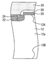
- FIG. 1 is a cross-sectional view of a semiconductor device 10 manufactured by the method of manufacturing a semiconductor device according to the first embodiment of the present invention.
- the semiconductor device 10 is a punch-through type IGBT.
- the semiconductor device 10 includes a semiconductor substrate 12 formed of, for example, n-type (hereinafter referred to as a first conductivity type) single crystal silicon.
- the semiconductor substrate 12 has a first major surface 12A and a second major surface 12B opposite to the first major surface 12A.
- a drift layer 12 a of the first conductivity type is formed on the semiconductor substrate 12.
- a buffer layer 14 of the first conductivity type in contact with the drift layer 12a is formed on the side of the second major surface 12B of the semiconductor substrate 12.
- the non-diffusion region 16 is on the side of the second major surface 12B of the buffer layer 14.
- the non-diffusion region 16 has the same impurity concentration as the drift layer 12a.
- a p-type (hereinafter referred to as a second conductivity type) collector layer 18 is formed on the side of the second major surface 12B of the non-diffusion region 16.
- a collector electrode 20 is formed in contact with the collector layer 18.
- a base layer 22 of the second conductivity type and an emitter layer 24 of the first conductivity type surrounded by the base layer 22 are formed on the side of the first major surface 12A of the semiconductor substrate 12.
- a gate insulating film 26 and a gate electrode 28 surrounded by the gate insulating film 26 are formed on the first major surface 12 A of the semiconductor substrate 12.
- An emitter electrode 30 is formed on the gate insulating film 26, the base layer 22, and the emitter layer 24.
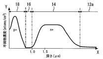
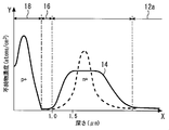
- FIG. 2 is a graph showing the impurity concentrations of the collector layer 18, the non-diffusion region 16, the buffer layer 14, and the drift layer 12a.
- FIG. 2 shows the impurity concentration of the second conductivity type of the collector layer 18, and the impurity concentration of the first conductivity type of the non-diffusion region 16, the buffer layer 14, and the drift layer 12a.
- the impurity concentration profile of the buffer layer 14 is trapezoidal with no maximum value.
- the impurity concentration of the non-diffusion region 16 is equal to the impurity concentration of the drift layer 12a.
- a method of manufacturing the semiconductor device according to the first embodiment of the present invention will be described. First, as shown in FIG. 3, the structure on the side of the first major surface 12A of the semiconductor substrate 12 is completed. Then, after a protective tape is attached to the emitter electrode 30, the semiconductor substrate 12 is ground from the second major surface 12B side. The thickness of the semiconductor substrate 12 after grinding is, eg, 100 ⁇ m.
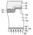
- FIG. 4 is a cross-sectional view of the semiconductor substrate for explaining the first step.
- the first conductivity type impurity 50 is implanted at an acceleration energy of 4 MeV.
- the first conductivity type impurity 52 is implanted to the second major surface 12B side more than the first conductivity type impurity 50 at an acceleration energy of 3 MeV.
- the first conductivity type impurity 54 is implanted to the second major surface 12 B side more than the first conductivity type impurity 52 at an acceleration energy of 2 MeV.
- Arrows in FIG. 4 indicate the ion implantation direction.
- the first conductivity type impurity 54 implanted at an acceleration energy of 2 MeV for example, reaches a location about 1.5 ⁇ m deep from the second major surface 12B.
- the first conductive impurities 50, 52, 54 are, for example, P (phosphorus), but are not particularly limited as long as they are the first conductive impurities. And the dose amount of these multiple (three times) ion implantation is uniform.
- a region of the semiconductor substrate 12 into which the first conductivity type impurities 50, 52, 54 are implanted is referred to as a first impurity region 56.
- FIG. 5 is a cross-sectional view of the semiconductor substrate for explaining the second step.
- the second conductivity type impurity 60 is implanted to the second main surface 12B side more than the first conductivity type impurity 54 at an acceleration energy of 100 keV. Arrows in FIG. 5 indicate the ion implantation direction.
- the second conductivity type impurity 60 is, for example, B (boron), but is not particularly limited as long as it is a second conductivity type impurity.
- a region of the semiconductor substrate 12 into which the second conductivity type impurity 60 is implanted is referred to as a second impurity region 62.
- the first impurity region 56 is formed by ion implantation at an acceleration energy of several MeV, while the second impurity region 62 is formed by ion implantation at an acceleration energy of 100 keV.
- the non-implanted region 64 where the impurity is not implanted remains between the impurity regions 62.
- the semiconductor substrate 12 is subjected to heat treatment.
- This process is referred to as a heat treatment process.
- the semiconductor substrate 12 is heated to, for example, about 300 to 500 ° C. using laser annealing or an electric furnace to activate the first conductivity type impurities 50, 52, 54 and the second conductivity type impurity 60.
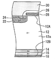
- FIG. 6 is a cross-sectional view of the semiconductor substrate 12 after the heat treatment step.
- the buffer layer 14 is formed of the first conductivity type impurities 50, 52, 54
- the collector layer 18 is formed of the second conductivity type impurity 60.
- a non-diffusion region 16 in which the first conductivity type impurities 50, 52 and 54 and the second conductivity type impurity 60 do not diffuse is left between the buffer layer 14 and the collector layer 18.
- the collector electrode 20 in contact with the collector layer 18 is formed.
- the semiconductor device 10 shown in FIG. 1 is completed.
- the turn-off operation of the semiconductor device 10 will now be described.
- the semiconductor device 10 is turned on and the positive voltage applied to the gate electrode 28 is lowered, the channel formed around the gate insulating film 26 disappears, and the electron injection from the emitter layer 24 to the drift layer 12 a stops.
- the potential of the buffer layer 14 rises, and the amount of holes supplied from the collector layer 18 to the drift layer 12 a decreases. Then, carriers (electrons and holes) accumulated in the drift layer 12a disappear as a pair. Alternatively, electrons in the drift layer 12a may flow to the collector electrode 20 side to be combined with holes and disappear, or holes in the drift layer 12a may flow from the base layer 22 to the emitter electrode 30 to combine with electrons and be eliminated. . When all the carriers in the drift layer 12a disappear, the drift layer 12a has a high resistance, and the turn-off is completed.
- the impurity amount of the buffer layer 14, that is, the total of the dose amount in the first step is set to an amount sufficient to stop the depletion layer.
- the method of manufacturing the semiconductor device of the comparative example is the method of manufacturing the semiconductor device according to the first embodiment of the present invention in that the first impurity region is formed by one ion implantation with acceleration energy of 3 MeV in the first step. It is different from The total of the dose amount of the first conductivity type impurity in the first step of the comparative example and the dose amount of the first conductivity type impurities 50, 52, 54 in the first step of the first embodiment is equal. Therefore, in the first step of the comparative example, a dose which is three times the first conductivity type impurity 50 is supplied in one ion implantation.
- FIG. 7 is a diagram showing the impurity concentration profile of the buffer layer of the comparative example by a broken line.
- the solid line shows the impurity concentration profile of buffer layer 14 of the first embodiment.
- the maximum value of the impurity concentration of the buffer layer is higher than the maximum value of the impurity concentration of the buffer layer 14. Since the buffer layer and the buffer layer 14 of the comparative example have the same impurity amount (dose amount), the area of the portion surrounded by the dashed line and the X axis in FIG. 7 and the solid line (buffer layer 14) in FIG. The areas of the parts that are cut are equal.
- the method of manufacturing a semiconductor device in accordance with the first embodiment of the present invention it is possible to manufacture a semiconductor device capable of supplying sufficient holes to the drift layer at turn-off while securing the withstand voltage.
- securing of the withstand voltage will be described.
- the semiconductor device 10 since the amount of impurities in the buffer layer 14 is an amount sufficient to stop the depletion layer at turn-off, the semiconductor device 10 has a withstand voltage.
- the maximum impurity concentration of the buffer layer is set so that the buffer layer 14 does not obstruct the flow of holes moving from the collector layer 18 to the drift layer 12a. It is preferable to make it low. Since the buffer layer 14 according to the first embodiment of the present invention is formed by performing heat treatment after performing ion implantation for a plurality of times with different acceleration energy, impurities are dispersed. Therefore, the maximum value of the impurity concentration of the buffer layer 14 can be lowered. Thus, a sufficient amount of holes can be supplied to the drift layer at turn-off.
- the semiconductor device 10 and the semiconductor device manufactured by the manufacturing method of the comparative example are compared. Both have equivalent withstand voltage characteristics because the dose of the buffer layer is equal. However, since the buffer layer 14 is formed by multiple ion implantation with different acceleration energy, the maximum value of the impurity concentration is low, whereas the buffer layer of the comparative example is formed by one ion implantation, so the maximum value of the impurity concentration Is high. Therefore, the semiconductor device 10 can supply sufficient holes to the drift layer 12a at turn-off, but the semiconductor device of the comparative example can not supply sufficient holes to the drift layer at turn-off. As described above, according to the method of manufacturing a semiconductor device according to the first embodiment of the present invention, it is possible to manufacture a semiconductor device capable of supplying a sufficient amount of holes to the drift layer at turn-off while securing the withstand voltage.
- the non-diffusion region 16 Since the holes in the collector layer 18 can easily proceed to the non-diffusion region 16, the non-diffusion region 16 has an effect of promoting the supply of holes to the drift layer 12a. Therefore, the semiconductor substrate 12 can be thinned to reduce the loss. Further, in the non-diffusion region 16, when the implantation energy is dispersed and the collector layer 18 moves to the first main surface 12 A side or the buffer layer 14 moves to the second main surface 12 B side, It has a function to prevent the buffer layer 14 from being in contact with it. By preventing the contact between the collector layer 18 and the buffer layer 14 by the non-diffusion region 16, the electrical characteristics of the semiconductor device 10 can be stabilized.
- the method of manufacturing a semiconductor device according to the first embodiment of the present invention is not limited to the planar IGBT described above, and for example, a current may be applied between the first main surface and the second main surface of a semiconductor substrate such as a trench IGBT or a diode. It can be used for elements of flowing structure.
- a current may be applied between the first main surface and the second main surface of a semiconductor substrate such as a trench IGBT or a diode. It can be used for elements of flowing structure.
- the n-type is the first conductivity type and the p-type is the second conductivity type
- the semiconductor device 10 may be formed with the p-type as the first conductivity type and the n-type as the second conductivity type.
- the first conductivity type impurities 50, 52, 54 must be implanted at high acceleration energy in the first step.
- the acceleration energy of the first conductivity type impurities 50, 52, 54 is preferably selected in the range of 1 to 10 MeV. In the first embodiment, 4, 3 and 2 MeV are selected. Note that the number of times of ion implantation in the first step may be two or more, and is not limited to three.
- the second conductivity type impurity 60 should be implanted at a low acceleration energy in the second step.
- the acceleration energy of the second conductivity type impurity 60 is preferably selected in the range of 5 to 100 keV. In the first embodiment, 100 keV is selected.
- the first conductivity type impurities 50, 52, 54 it is preferable to implant the first conductivity type impurities 50, 52, 54 as far as possible from the second major surface 12B. Therefore, in the first step, the first conductivity type impurities 50, 52, 54 may be implanted perpendicularly to the second major surface 12B to intentionally cause channeling. Thereby, the first conductivity type impurities 50, 52, 54 can reach the deep position of the semiconductor substrate 12.
- protons may be injected as the first conductivity type impurity.
- the proton implantation is suitable for introducing a defect in a deep position of the semiconductor substrate, so that the non-diffusion region 16 can be easily provided.
- the impurity concentration profile of the buffer layer 14 is not limited to the trapezoidal shape of FIG.
- the above effect can be obtained even with the impurity concentration profile of the buffer layer 70 shown in FIG.
- the maximum value of the impurity concentration of buffer layer 70 is approximately equal to the maximum value of the impurity concentration of buffer layer 14 of the first embodiment.
- FIG. 9 is a cross-sectional view for explaining the first step of the second embodiment of the present invention. A plurality of ion implantations in the first step are performed such that the dose of the first conductivity type impurity is increased toward the second main surface 12B.
- the first conductivity type impurity 80 is implanted at an acceleration energy of 4 MeV. Then, the first conductivity type impurity 82 is implanted so that the dose amount is larger than the first conductivity type impurity 80 at an acceleration energy of 3 MeV. Next, the first conductivity type impurity 84 is implanted so that the dose amount is larger than that of the first conductivity type impurity 82 at an acceleration energy of 2 MeV.
- the dose of the first conductivity type impurity 84 is larger than the dose of the first conductivity type impurity 82.
- the dose of the first conductivity type impurity 82 is larger than the dose of the first conductivity type impurity 80.
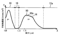
- the impurity concentration profile of the buffer layer 90 shown by the solid line in FIG. 10 can be obtained.
- the impurity concentration profile of the buffer layer 90 has a slope 90a which gently rises toward the second major surface 12B.
- the broken line shows the impurity concentration profile of buffer layer 14 of the first embodiment.
- the same effect as that of the first embodiment can be obtained. Furthermore, since the impurity concentration profile of buffer layer 90 has slope 90a shown in FIG. 10, the electric field strength of buffer layer 90 during the turn-off operation is relaxed. That is, when the depletion layer extends from the side of the first main surface 12A to the buffer layer at turn-off, the impurity concentration rapidly increases from the first main surface 12A to the second main surface 12B in the impurity concentration profile of broken line in FIG. Because the electric field is easy to concentrate. However, in the buffer layer 90, the impurity concentration rises gradually due to the slope 90a, so electric field concentration hardly occurs. As a result, it is possible to suppress the sudden rise of the surge voltage, and the oscillation can be reliably suppressed.
Landscapes
- Electrodes Of Semiconductors (AREA)
- Insulated Gate Type Field-Effect Transistor (AREA)
- Thyristors (AREA)
Abstract
Description
図1は、本発明の実施の形態1に係る半導体装置の製造方法で製造された半導体装置10の断面図である。半導体装置10はパンチスルー型IGBTである。半導体装置10は例えばn型(以後、第1導電型という)の単結晶シリコンで形成された半導体基板12を備えている。半導体基板12は第1主面12Aと、第1主面12Aと反対の面である第2主面12Bとを有している。半導体基板12には第1導電型のドリフト層12aが形成されている。
本発明の実施の形態2に係る半導体装置の製造方法は、実施の形態1との共通点が多いので、実施の形態1との相違点を中心に説明する。図9は、本発明の実施の形態2の第1工程を説明する断面図である。第1工程における複数回のイオン注入は、第2主面12B側ほど第1導電型不純物のドーズ量が多くなるように行う。
Claims (6)
- 第1主面と前記第1主面と反対の面である第2主面とを有する半導体基板の前記第2主面に、加速エネルギの異なる複数回のイオン注入で第1導電型不純物を注入し、前記半導体基板に第1不純物領域を形成する第1工程と、
前記第2主面に、前記複数回のイオン注入よりも低い加速エネルギで第2導電型不純物をイオン注入し、前記半導体基板に、前記第1不純物領域との間に不純物が注入されない無注入領域を残すように第2不純物領域を形成する第2工程と、
前記第1導電型不純物でバッファ層を形成し、前記第2導電型不純物でコレクタ層を形成し、前記バッファ層と前記コレクタ層の間に前記第1導電型不純物と前記第2導電型不純物が拡散しない無拡散領域を残すように前記半導体基板に熱処理を施す熱処理工程と、
前記コレクタ層に接するコレクタ電極を形成する工程と、を備えたことを特徴とする半導体装置の製造方法。 - 前記第1導電型不純物は、1~10MeVの加速エネルギで前記第2主面に注入し、
前記第2導電型不純物は、5~100keVの加速エネルギで前記第2主面に注入することを特徴とする請求項1に記載の半導体装置の製造方法。 - 前記複数回のイオン注入のドーズ量は均一であることを特徴とする請求項1又は2に記載の半導体装置の製造方法。
- 前記複数回のイオン注入は、前記第2主面側ほど前記第1導電型不純物のドーズ量が多くなるように行うことを特徴とする請求項1又は2に記載の半導体装置の製造方法。
- 前記第1工程では、前記第2主面に対して垂直に前記第1導電型不純物を注入することを特徴とする請求項1~4のいずれか1項に記載の半導体装置の製造方法。
- 前記第1工程では、前記第1導電型不純物としてプロトンを注入することを特徴とする請求項1~4のいずれか1項に記載の半導体装置の製造方法。
Priority Applications (7)
| Application Number | Priority Date | Filing Date | Title |
|---|---|---|---|
| US15/031,623 US9673308B2 (en) | 2013-12-13 | 2013-12-13 | Semiconductor device manufacturing method |
| PCT/JP2013/083458 WO2015087439A1 (ja) | 2013-12-13 | 2013-12-13 | 半導体装置の製造方法 |
| EP13898991.8A EP3082167B1 (en) | 2013-12-13 | 2013-12-13 | Semiconductor device manufacturing method |
| KR1020167015446A KR101838829B1 (ko) | 2013-12-13 | 2013-12-13 | 반도체 장치의 제조 방법 |
| JP2015552265A JP6149942B2 (ja) | 2013-12-13 | 2013-12-13 | 半導体装置の製造方法 |
| CN201380081607.0A CN105830220B (zh) | 2013-12-13 | 2013-12-13 | 半导体装置的制造方法 |
| TW103104017A TWI553714B (zh) | 2013-12-13 | 2014-02-07 | 半導體裝置之製造方法 |
Applications Claiming Priority (1)
| Application Number | Priority Date | Filing Date | Title |
|---|---|---|---|
| PCT/JP2013/083458 WO2015087439A1 (ja) | 2013-12-13 | 2013-12-13 | 半導体装置の製造方法 |
Publications (1)
| Publication Number | Publication Date |
|---|---|
| WO2015087439A1 true WO2015087439A1 (ja) | 2015-06-18 |
Family
ID=53370780
Family Applications (1)
| Application Number | Title | Priority Date | Filing Date |
|---|---|---|---|
| PCT/JP2013/083458 Ceased WO2015087439A1 (ja) | 2013-12-13 | 2013-12-13 | 半導体装置の製造方法 |
Country Status (7)
| Country | Link |
|---|---|
| US (1) | US9673308B2 (ja) |
| EP (1) | EP3082167B1 (ja) |
| JP (1) | JP6149942B2 (ja) |
| KR (1) | KR101838829B1 (ja) |
| CN (1) | CN105830220B (ja) |
| TW (1) | TWI553714B (ja) |
| WO (1) | WO2015087439A1 (ja) |
Cited By (4)
| Publication number | Priority date | Publication date | Assignee | Title |
|---|---|---|---|---|
| US11635458B2 (en) | 2021-04-20 | 2023-04-25 | Fuji Electric Co., Ltd. | Analyzing apparatus, analysis method, and computer-readable medium |
| JPWO2023157330A1 (ja) * | 2022-02-17 | 2023-08-24 | ||
| US12453110B2 (en) | 2021-04-20 | 2025-10-21 | Fuji Electric Co., Ltd. | Semiconductor device |
| US12615811B2 (en) | 2022-02-17 | 2026-04-28 | Fuji Electric Co., Ltd. | Semiconductor device to suppress leakage current |
Families Citing this family (4)
| Publication number | Priority date | Publication date | Assignee | Title |
|---|---|---|---|---|
| US9825128B2 (en) * | 2015-10-20 | 2017-11-21 | Maxpower Semiconductor, Inc. | Vertical power transistor with thin bottom emitter layer and dopants implanted in trenches in shield area and termination rings |
| JP6964566B2 (ja) * | 2018-08-17 | 2021-11-10 | 三菱電機株式会社 | 半導体装置およびその製造方法 |
| CN113948375A (zh) * | 2020-07-16 | 2022-01-18 | 珠海格力电器股份有限公司 | 一种提高半导体有源区杂质激活率的方法及其应用 |
| CN114335143B (zh) * | 2021-12-29 | 2025-08-12 | 深圳市千屹芯科技有限公司 | 低关断电流拖尾的超级结igbt及其制作方法 |
Citations (3)
| Publication number | Priority date | Publication date | Assignee | Title |
|---|---|---|---|---|
| JP2001077357A (ja) | 1999-08-31 | 2001-03-23 | Toshiba Corp | 半導体装置 |
| WO2013147275A1 (ja) * | 2012-03-30 | 2013-10-03 | 富士電機株式会社 | 半導体装置の製造方法 |
| WO2013147274A1 (ja) * | 2012-03-30 | 2013-10-03 | 富士電機株式会社 | 半導体装置の製造方法 |
Family Cites Families (11)
| Publication number | Priority date | Publication date | Assignee | Title |
|---|---|---|---|---|
| US6482681B1 (en) | 2000-05-05 | 2002-11-19 | International Rectifier Corporation | Hydrogen implant for buffer zone of punch-through non epi IGBT |
| JP3906076B2 (ja) * | 2001-01-31 | 2007-04-18 | 株式会社東芝 | 半導体装置 |
| JP2004079878A (ja) * | 2002-08-21 | 2004-03-11 | Toshiba Corp | 半導体装置及びその製造方法 |
| JP2004247593A (ja) | 2003-02-14 | 2004-09-02 | Toshiba Corp | 半導体装置及びその製造方法 |
| DE102005026408B3 (de) | 2005-06-08 | 2007-02-01 | Infineon Technologies Ag | Verfahren zur Herstellung einer Stoppzone in einem Halbleiterkörper und Halbleiterbauelement mit einer Stoppzone |
| DE102005049506B4 (de) * | 2005-10-13 | 2011-06-09 | Infineon Technologies Austria Ag | Vertikales Halbleiterbauelement |
| JP5155536B2 (ja) * | 2006-07-28 | 2013-03-06 | 一般財団法人電力中央研究所 | SiC結晶の質を向上させる方法およびSiC半導体素子の製造方法 |
| JP5365009B2 (ja) | 2008-01-23 | 2013-12-11 | 富士電機株式会社 | 半導体装置およびその製造方法 |
| EP3734645B1 (en) * | 2010-12-24 | 2025-09-10 | Qualcomm Incorporated | Trap rich layer for semiconductor devices |
| JP5639940B2 (ja) * | 2011-03-25 | 2014-12-10 | 新電元工業株式会社 | 絶縁ゲート型バイポーラトランジスタ |
| KR20120140411A (ko) * | 2011-06-21 | 2012-12-31 | (주) 트리노테크놀로지 | 전력 반도체 소자 및 그 제조 방법 |
-
2013
- 2013-12-13 CN CN201380081607.0A patent/CN105830220B/zh active Active
- 2013-12-13 WO PCT/JP2013/083458 patent/WO2015087439A1/ja not_active Ceased
- 2013-12-13 KR KR1020167015446A patent/KR101838829B1/ko active Active
- 2013-12-13 US US15/031,623 patent/US9673308B2/en active Active
- 2013-12-13 JP JP2015552265A patent/JP6149942B2/ja active Active
- 2013-12-13 EP EP13898991.8A patent/EP3082167B1/en active Active
-
2014
- 2014-02-07 TW TW103104017A patent/TWI553714B/zh active
Patent Citations (3)
| Publication number | Priority date | Publication date | Assignee | Title |
|---|---|---|---|---|
| JP2001077357A (ja) | 1999-08-31 | 2001-03-23 | Toshiba Corp | 半導体装置 |
| WO2013147275A1 (ja) * | 2012-03-30 | 2013-10-03 | 富士電機株式会社 | 半導体装置の製造方法 |
| WO2013147274A1 (ja) * | 2012-03-30 | 2013-10-03 | 富士電機株式会社 | 半導体装置の製造方法 |
Non-Patent Citations (1)
| Title |
|---|
| See also references of EP3082167A4 |
Cited By (5)
| Publication number | Priority date | Publication date | Assignee | Title |
|---|---|---|---|---|
| US11635458B2 (en) | 2021-04-20 | 2023-04-25 | Fuji Electric Co., Ltd. | Analyzing apparatus, analysis method, and computer-readable medium |
| US12453110B2 (en) | 2021-04-20 | 2025-10-21 | Fuji Electric Co., Ltd. | Semiconductor device |
| JPWO2023157330A1 (ja) * | 2022-02-17 | 2023-08-24 | ||
| JP7687514B2 (ja) | 2022-02-17 | 2025-06-03 | 富士電機株式会社 | 半導体装置およびその製造方法 |
| US12615811B2 (en) | 2022-02-17 | 2026-04-28 | Fuji Electric Co., Ltd. | Semiconductor device to suppress leakage current |
Also Published As
| Publication number | Publication date |
|---|---|
| KR101838829B1 (ko) | 2018-03-14 |
| EP3082167A4 (en) | 2017-08-02 |
| JPWO2015087439A1 (ja) | 2017-03-16 |
| JP6149942B2 (ja) | 2017-06-21 |
| TWI553714B (zh) | 2016-10-11 |
| CN105830220B (zh) | 2019-05-28 |
| US9673308B2 (en) | 2017-06-06 |
| KR20160086368A (ko) | 2016-07-19 |
| CN105830220A (zh) | 2016-08-03 |
| EP3082167A1 (en) | 2016-10-19 |
| EP3082167B1 (en) | 2021-02-17 |
| US20160254372A1 (en) | 2016-09-01 |
| TW201523708A (zh) | 2015-06-16 |
Similar Documents
| Publication | Publication Date | Title |
|---|---|---|
| US20200144360A1 (en) | Method of manufacturing a semiconductor device | |
| CN107710417B (zh) | 半导体装置的制造方法 | |
| US11152224B2 (en) | Semiconductor device with field stop layer and semiconductor device manufacturing method thereof | |
| CN107924843B (zh) | 制造碳化硅功率半导体器件的边缘终端的方法和碳化硅功率半导体器件 | |
| US9954086B2 (en) | Semiconductor device having multiple field stop layers | |
| US9570541B2 (en) | Semiconductor device and method of manufacturing the same | |
| JP6149942B2 (ja) | 半導体装置の製造方法 | |
| CN109103247B (zh) | 半导体装置及其制造方法 | |
| WO2016147264A1 (ja) | 半導体装置及びその製造方法 | |
| US9704980B2 (en) | Insulated gate bipolar transistor and method for manufacturing same | |
| CN105280485A (zh) | 制造包括场停止区的半导体器件的方法 | |
| JP2018078216A (ja) | 半導体装置およびその製造方法 | |
| US20100117117A1 (en) | Vertical IGBT Device | |
| US7629665B2 (en) | Semiconductor component with a channel stop zone | |
| JP5992216B2 (ja) | バイポーラ・パンチ・スルー半導体デバイス及びそのような半導体デバイスを製造するための方法 | |
| JP5565134B2 (ja) | 半導体装置の製造方法 | |
| CN114695513B (zh) | 半导体装置及其制造方法 | |
| CN105322003A (zh) | 绝缘栅双极型晶体管及其制备方法 | |
| CN108649064B (zh) | 一种提高uis雪崩耐量的mosfet及其制备方法 | |
| JP2017188569A (ja) | 半導体装置およびその製造方法 | |
| JP2014056881A (ja) | 半導体装置および半導体装置の製造方法 | |
| JP2010034281A (ja) | 半導体装置及びその製造方法 |
Legal Events
| Date | Code | Title | Description |
|---|---|---|---|
| 121 | Ep: the epo has been informed by wipo that ep was designated in this application |
Ref document number: 13898991 Country of ref document: EP Kind code of ref document: A1 |
|
| ENP | Entry into the national phase |
Ref document number: 2015552265 Country of ref document: JP Kind code of ref document: A |
|
| WWE | Wipo information: entry into national phase |
Ref document number: 15031623 Country of ref document: US |
|
| REEP | Request for entry into the european phase |
Ref document number: 2013898991 Country of ref document: EP |
|
| WWE | Wipo information: entry into national phase |
Ref document number: 2013898991 Country of ref document: EP |
|
| ENP | Entry into the national phase |
Ref document number: 20167015446 Country of ref document: KR Kind code of ref document: A |
|
| NENP | Non-entry into the national phase |
Ref country code: DE |