WO2015105109A1 - プリント配線板用絶縁層及びプリント配線板 - Google Patents
プリント配線板用絶縁層及びプリント配線板 Download PDFInfo
- Publication number
- WO2015105109A1 WO2015105109A1 PCT/JP2015/050188 JP2015050188W WO2015105109A1 WO 2015105109 A1 WO2015105109 A1 WO 2015105109A1 JP 2015050188 W JP2015050188 W JP 2015050188W WO 2015105109 A1 WO2015105109 A1 WO 2015105109A1
- Authority
- WO
- WIPO (PCT)
- Prior art keywords
- insulating layer
- printed wiring
- group
- alkenyl
- mass
- Prior art date
- Legal status (The legal status is an assumption and is not a legal conclusion. Google has not performed a legal analysis and makes no representation as to the accuracy of the status listed.)
- Ceased
Links
Classifications
-
- H—ELECTRICITY
- H05—ELECTRIC TECHNIQUES NOT OTHERWISE PROVIDED FOR
- H05K—PRINTED CIRCUITS; CASINGS OR CONSTRUCTIONAL DETAILS OF ELECTRIC APPARATUS; MANUFACTURE OF ASSEMBLAGES OF ELECTRICAL COMPONENTS
- H05K1/00—Printed circuits
- H05K1/02—Details
- H05K1/0271—Arrangements for reducing stress or warp in rigid printed circuit boards, e.g. caused by loads, vibrations or differences in thermal expansion
-
- B—PERFORMING OPERATIONS; TRANSPORTING
- B32—LAYERED PRODUCTS
- B32B—LAYERED PRODUCTS, i.e. PRODUCTS BUILT-UP OF STRATA OF FLAT OR NON-FLAT, e.g. CELLULAR OR HONEYCOMB, FORM
- B32B15/00—Layered products comprising a layer of metal
- B32B15/04—Layered products comprising a layer of metal comprising metal as the main or only constituent of a layer, which is next to another layer of the same or of a different material
- B32B15/08—Layered products comprising a layer of metal comprising metal as the main or only constituent of a layer, which is next to another layer of the same or of a different material of synthetic resin
-
- C—CHEMISTRY; METALLURGY
- C08—ORGANIC MACROMOLECULAR COMPOUNDS; THEIR PREPARATION OR CHEMICAL WORKING-UP; COMPOSITIONS BASED THEREON
- C08J—WORKING-UP; GENERAL PROCESSES OF COMPOUNDING; AFTER-TREATMENT NOT COVERED BY SUBCLASSES C08B, C08C, C08F, C08G or C08H
- C08J5/00—Manufacture of articles or shaped materials containing macromolecular substances
- C08J5/04—Reinforcing macromolecular compounds with loose or coherent fibrous material
- C08J5/0405—Reinforcing macromolecular compounds with loose or coherent fibrous material with inorganic fibres
- C08J5/043—Reinforcing macromolecular compounds with loose or coherent fibrous material with inorganic fibres with glass fibres
-
- C—CHEMISTRY; METALLURGY
- C08—ORGANIC MACROMOLECULAR COMPOUNDS; THEIR PREPARATION OR CHEMICAL WORKING-UP; COMPOSITIONS BASED THEREON
- C08J—WORKING-UP; GENERAL PROCESSES OF COMPOUNDING; AFTER-TREATMENT NOT COVERED BY SUBCLASSES C08B, C08C, C08F, C08G or C08H
- C08J5/00—Manufacture of articles or shaped materials containing macromolecular substances
- C08J5/24—Impregnating materials with prepolymers which can be polymerised in situ, e.g. manufacture of prepregs
- C08J5/241—Impregnating materials with prepolymers which can be polymerised in situ, e.g. manufacture of prepregs using inorganic fibres
- C08J5/244—Impregnating materials with prepolymers which can be polymerised in situ, e.g. manufacture of prepregs using inorganic fibres using glass fibres
-
- H—ELECTRICITY
- H05—ELECTRIC TECHNIQUES NOT OTHERWISE PROVIDED FOR
- H05K—PRINTED CIRCUITS; CASINGS OR CONSTRUCTIONAL DETAILS OF ELECTRIC APPARATUS; MANUFACTURE OF ASSEMBLAGES OF ELECTRICAL COMPONENTS
- H05K1/00—Printed circuits
- H05K1/02—Details
- H05K1/0296—Conductive pattern lay-out details not covered by sub groups H05K1/02 - H05K1/0295
- H05K1/0298—Multilayer circuits
-
- H—ELECTRICITY
- H05—ELECTRIC TECHNIQUES NOT OTHERWISE PROVIDED FOR
- H05K—PRINTED CIRCUITS; CASINGS OR CONSTRUCTIONAL DETAILS OF ELECTRIC APPARATUS; MANUFACTURE OF ASSEMBLAGES OF ELECTRICAL COMPONENTS
- H05K1/00—Printed circuits
- H05K1/02—Details
- H05K1/03—Use of materials for the substrate
- H05K1/0313—Organic insulating material
- H05K1/0353—Organic insulating material consisting of two or more materials, e.g. two or more polymers, polymer + filler, + reinforcement
- H05K1/0373—Organic insulating material consisting of two or more materials, e.g. two or more polymers, polymer + filler, + reinforcement containing additives, e.g. fillers
-
- H—ELECTRICITY
- H05—ELECTRIC TECHNIQUES NOT OTHERWISE PROVIDED FOR
- H05K—PRINTED CIRCUITS; CASINGS OR CONSTRUCTIONAL DETAILS OF ELECTRIC APPARATUS; MANUFACTURE OF ASSEMBLAGES OF ELECTRICAL COMPONENTS
- H05K1/00—Printed circuits
- H05K1/02—Details
- H05K1/03—Use of materials for the substrate
- H05K1/0393—Flexible materials
-
- H—ELECTRICITY
- H05—ELECTRIC TECHNIQUES NOT OTHERWISE PROVIDED FOR
- H05K—PRINTED CIRCUITS; CASINGS OR CONSTRUCTIONAL DETAILS OF ELECTRIC APPARATUS; MANUFACTURE OF ASSEMBLAGES OF ELECTRICAL COMPONENTS
- H05K3/00—Apparatus or processes for manufacturing printed circuits
- H05K3/02—Apparatus or processes for manufacturing printed circuits in which the conductive material is applied to the surface of the insulating support and is thereafter removed from such areas of the surface which are not intended for current conducting or shielding
- H05K3/022—Processes for manufacturing precursors of printed circuits, i.e. copper-clad substrates
-
- H—ELECTRICITY
- H05—ELECTRIC TECHNIQUES NOT OTHERWISE PROVIDED FOR
- H05K—PRINTED CIRCUITS; CASINGS OR CONSTRUCTIONAL DETAILS OF ELECTRIC APPARATUS; MANUFACTURE OF ASSEMBLAGES OF ELECTRICAL COMPONENTS
- H05K3/00—Apparatus or processes for manufacturing printed circuits
- H05K3/46—Manufacturing multilayer circuits
- H05K3/4644—Manufacturing multilayer circuits by building the multilayer layer by layer, i.e. build-up multilayer circuits
-
- C—CHEMISTRY; METALLURGY
- C08—ORGANIC MACROMOLECULAR COMPOUNDS; THEIR PREPARATION OR CHEMICAL WORKING-UP; COMPOSITIONS BASED THEREON
- C08J—WORKING-UP; GENERAL PROCESSES OF COMPOUNDING; AFTER-TREATMENT NOT COVERED BY SUBCLASSES C08B, C08C, C08F, C08G or C08H
- C08J2379/00—Characterised by the use of macromolecular compounds obtained by reactions forming in the main chain of the macromolecule a linkage containing nitrogen with or without oxygen, or carbon only, not provided for in groups C08J2361/00 - C08J2377/00
- C08J2379/04—Polycondensates having nitrogen-containing heterocyclic rings in the main chain; Polyhydrazides; Polyamide acids or similar polyimide precursors
- C08J2379/08—Polyimides; Polyester-imides; Polyamide-imides; Polyamide acids or similar polyimide precursors
-
- C—CHEMISTRY; METALLURGY
- C08—ORGANIC MACROMOLECULAR COMPOUNDS; THEIR PREPARATION OR CHEMICAL WORKING-UP; COMPOSITIONS BASED THEREON
- C08J—WORKING-UP; GENERAL PROCESSES OF COMPOUNDING; AFTER-TREATMENT NOT COVERED BY SUBCLASSES C08B, C08C, C08F, C08G or C08H
- C08J2465/00—Characterised by the use of macromolecular compounds obtained by reactions forming a carbon-to-carbon link in the main chain; Derivatives of such polymers
-
- C—CHEMISTRY; METALLURGY
- C08—ORGANIC MACROMOLECULAR COMPOUNDS; THEIR PREPARATION OR CHEMICAL WORKING-UP; COMPOSITIONS BASED THEREON
- C08J—WORKING-UP; GENERAL PROCESSES OF COMPOUNDING; AFTER-TREATMENT NOT COVERED BY SUBCLASSES C08B, C08C, C08F, C08G or C08H
- C08J2479/00—Characterised by the use of macromolecular compounds obtained by reactions forming in the main chain of the macromolecule a linkage containing nitrogen with or without oxygen, or carbon only, not provided for in groups C08J2461/00 - C08J2477/00
- C08J2479/04—Polycondensates having nitrogen-containing heterocyclic rings in the main chain; Polyhydrazides; Polyamide acids or similar polyimide precursors
-
- H—ELECTRICITY
- H05—ELECTRIC TECHNIQUES NOT OTHERWISE PROVIDED FOR
- H05K—PRINTED CIRCUITS; CASINGS OR CONSTRUCTIONAL DETAILS OF ELECTRIC APPARATUS; MANUFACTURE OF ASSEMBLAGES OF ELECTRICAL COMPONENTS
- H05K1/00—Printed circuits
- H05K1/02—Details
- H05K1/03—Use of materials for the substrate
- H05K1/0313—Organic insulating material
- H05K1/0353—Organic insulating material consisting of two or more materials, e.g. two or more polymers, polymer + filler, + reinforcement
- H05K1/036—Multilayers with layers of different types
-
- H—ELECTRICITY
- H05—ELECTRIC TECHNIQUES NOT OTHERWISE PROVIDED FOR
- H05K—PRINTED CIRCUITS; CASINGS OR CONSTRUCTIONAL DETAILS OF ELECTRIC APPARATUS; MANUFACTURE OF ASSEMBLAGES OF ELECTRICAL COMPONENTS
- H05K1/00—Printed circuits
- H05K1/02—Details
- H05K1/03—Use of materials for the substrate
- H05K1/0313—Organic insulating material
- H05K1/0353—Organic insulating material consisting of two or more materials, e.g. two or more polymers, polymer + filler, + reinforcement
- H05K1/0366—Organic insulating material consisting of two or more materials, e.g. two or more polymers, polymer + filler, + reinforcement reinforced, e.g. by fibres, fabrics
-
- H—ELECTRICITY
- H05—ELECTRIC TECHNIQUES NOT OTHERWISE PROVIDED FOR
- H05K—PRINTED CIRCUITS; CASINGS OR CONSTRUCTIONAL DETAILS OF ELECTRIC APPARATUS; MANUFACTURE OF ASSEMBLAGES OF ELECTRICAL COMPONENTS
- H05K2201/00—Indexing scheme relating to printed circuits covered by H05K1/00
- H05K2201/03—Conductive materials
- H05K2201/0332—Structure of the conductor
- H05K2201/0335—Layered conductors or foils
- H05K2201/0355—Metal foils
-
- H—ELECTRICITY
- H05—ELECTRIC TECHNIQUES NOT OTHERWISE PROVIDED FOR
- H05K—PRINTED CIRCUITS; CASINGS OR CONSTRUCTIONAL DETAILS OF ELECTRIC APPARATUS; MANUFACTURE OF ASSEMBLAGES OF ELECTRICAL COMPONENTS
- H05K2201/00—Indexing scheme relating to printed circuits covered by H05K1/00
- H05K2201/09—Shape and layout
- H05K2201/09009—Substrate related
- H05K2201/09136—Means for correcting warpage
Definitions
- the present invention relates to an insulating layer for a printed wiring board.
- One of the measures is to reduce the thermal expansion of the insulating layer used for the printed wiring board. This is a technique for suppressing warpage by bringing the thermal expansion coefficient of a printed wiring board close to the thermal expansion coefficient of a semiconductor element, and is currently being actively worked on (see, for example, Patent Documents 1 to 3).
- methods for suppressing the warpage of the semiconductor plastic package include increasing the rigidity of the laminated board (higher rigidity) and increasing the glass transition temperature of the laminated board (high Tg). (For example, see Patent Documents 4 and 5).
- JP 2013-216884 A Japanese Patent No. 3173332 JP 2009-035728 A JP 2013-001807 A JP2011-177892A
- the high rigidity of the laminated board can be achieved by highly filling the resin composition used for the laminated board with an inorganic filler having a high elastic modulus such as alumina.
- an inorganic filler having a high elastic modulus such as alumina deteriorates the moldability of the laminate, and the use of an inorganic filler such as alumina has the problem of deteriorating the thermal expansion coefficient of the laminate. Therefore, the increase in rigidity of the laminated plate cannot sufficiently achieve the suppression of the warp of the semiconductor plastic package.
- the technique of increasing the Tg of the laminated plate improves the elastic modulus during reflow, and thus is effective in reducing the warpage of the semiconductor plastic package.
- the technique using high Tg causes deterioration in moisture absorption heat resistance due to an increase in crosslink density and voids due to deterioration in moldability. Therefore, it is practically used in the field of electronic materials that require extremely high reliability. Often problematic. Therefore, a method for solving these problems is desired.
- An object of the present invention is to provide an insulating layer for a printed wiring board that can reduce, for example, warpage during manufacturing of a semiconductor plastic package by using a method different from the conventional one.
- Another object of the present invention is to provide an insulating layer for a printed wiring board having good moldability and excellent heat resistance and thermal elastic modulus.
- the present inventors have determined that the difference between the bending elastic modulus at 25 ° C. and the bending elastic modulus at 250 ° C. is 20% or less (for example, an insulating layer for printed wiring boards)
- the metal foil-clad laminate has been found to effectively suppress warping of a semiconductor plastic package, for example, and has reached the present invention.
- the resin composition used for the insulating layer for printed wiring boards includes alkenyl-substituted nadiimide (A), maleimide compound (B), cyanate ester compound (C) and inorganic filler (D), and the cyanic acid
- the content of the ester compound (C) is 5 to 15 parts by mass with respect to a total of 100 parts by mass of the components (A) to (C), and the number of alkenyl groups ( ⁇ ) of the alkenyl-substituted nadiimide (A) and the
- the maleimide group number ( ⁇ ) ratio ([ ⁇ / ⁇ ]) of the maleimide compound (B) is 0.9 to 4.3, the moldability is good and the heat resistance and heat
- the present inventors have found that an insulating layer for printed wiring boards having an excellent time elastic modulus can be provided, and reached the present invention.
- the present invention relates to the following.
- An insulating layer for printed wiring boards wherein a difference between a flexural modulus at 25 ° C. and a thermal flex modulus at 250 ° C. is 20% or less.
- the insulating layer includes a resin composition;
- the resin composition includes an alkenyl-substituted nadiimide (A), a maleimide compound (B), a cyanate ester compound (C), and an inorganic filler (D), and the content of the cyanate ester compound (C) is a component.
- each R 1 independently represents a hydrogen atom or an alkyl group having 1 to 6 carbon atoms
- R 2 represents an alkylene group having 1 to 6 carbon atoms, a phenylene group, a biphenylene group, a naphthylene group, or The group represented by the general formula (2) or (3) is shown.
- R 3 represents a substituent represented by a methylene group, an isopropylidene group, CO, O, S, or SO 2.
- each R 4 independently represents an alkylene group having 1 to 4 carbon atoms or a cycloalkylene group having 5 to 8 carbon atoms.
- each R 4 independently represents an alkylene group having 1 to 4 carbon atoms or a cycloalkylene group having 5 to 8 carbon atoms.
- the maleimide compound (B) is bis (4-maleimidophenyl) methane, 2,2-bis ⁇ 4- (4-maleimidophenoxy) -phenyl ⁇ propane, bis (3-ethyl-5-methyl-4-maleimidophenyl)
- R 5 each independently represents a hydrogen atom or a methyl group, and n 1 represents an integer of 1 or more.
- each R 6 independently represents a hydrogen atom or a methyl group, and n 2 represents an integer of 1 or more.
- R 7 each independently represents a hydrogen atom or a methyl group, and n 3 represents an integer of 1 or more.
- the insulating layer is a metal foil-clad laminate obtained by laminating and curing at least one selected from the group consisting of a resin sheet and a prepreg and a metal foil.
- a printed wiring board comprising the insulating layer for a printed wiring board according to any one of [1] to [11] and a conductor layer formed on a surface of the insulating layer.
- an insulating layer having a difference between a bending elastic modulus at 25 ° C. and a bending elastic modulus at 250 ° C. within 20% is used for a printed wiring board material used for a semiconductor plastic package.
- warpage of the semiconductor plastic package is suppressed, and it becomes possible to manufacture a semiconductor plastic package with excellent yield and reliability during manufacturing.
- an insulating layer for printed wiring boards (for example, a laminated board or a copper clad laminated board) having good moldability and excellent heat resistance and thermal elastic modulus can be provided. Furthermore, such an insulating layer for a printed wiring board can provide a printed wiring board that has good moldability and maintains an excellent elastic modulus even at a high temperature of 250 ° C., which is close to the reflow temperature during semiconductor mounting. .
- the insulating layer for printed wiring boards of the present embodiment (hereinafter also simply referred to as “insulating layer”) has a difference between the bending elastic modulus at 25 ° C. and the bending elastic modulus at 250 ° C. of 20% or less. It is preferably ⁇ 20%, more preferably 0 to 15%.
- the form of the insulating layer for printed wiring board is not particularly limited.
- the insulating layer for printed wiring board such as glass fiber cloth, organic fiber cloth, glass fiber nonwoven cloth, and organic fiber nonwoven cloth is well known.
- a prepreg impregnated with an arbitrary thermosetting resin or thermoplastic resin, a metal foil-clad laminate formed by laminating this and a metal foil, and these insulating resins to a metal foil or film examples thereof include embedded sheets in a coated form, resin sheets and films including polyimide, and metal foil-clad laminates formed by laminating these sheets and films and metal foils.
- the embedded sheet is not particularly limited.
- CRS sheet obtained by applying a resin to a copper foil and drying
- FRS Alignomoto ABF: obtained by applying a resin to a film and drying
- the resin sheet and the film are not particularly limited, and examples thereof include a flexible substrate in which wiring is performed by directly plating a film or resin.
- the method for setting the difference between the bending elastic modulus at 25 ° C. and the bending elastic modulus at 250 ° C. within 20% of the insulating layer of this embodiment to 20% or less is not particularly limited, for example, a resin composition used for the insulating layer There is a method of appropriately adjusting the type and content of each component of the product.
- an existing method can be used as long as the object of the present invention is not impaired.
- a technique for constraining molecular motion by introducing nanofillers a technique for hybridizing nanosilica to the crosslinking point of the resin used for the insulating layer by a sol-gel method, or a high Tg for the resin itself used for the insulating layer
- a technique such as Tg-less in a region of 400 ° C. or lower a technique for constraining molecular motion by introducing nanofillers, a technique for hybridizing nanosilica to the crosslinking point of the resin used for the insulating layer by a sol-gel method, or a high Tg for the resin itself used for the insulating layer.
- a technique such as Tg-less in a region of 400 ° C. or lower a technique for constraining molecular motion by introducing nanofillers, a technique for hybridizing nanosilica to the crosslinking point of the resin used for the insulating layer by a sol-gel method, or a
- a warpage reduction technique used conventionally.
- a technique is not particularly limited, and examples thereof include a technique of imparting low thermal expansibility and high elastic modulus by adding an inorganic filler or a stress relaxation component.
- the resin used for the insulating layer itself has a high Tg, 400 ° C.
- the resin used for the insulating layer is not particularly limited, but from the viewpoint of insulation reliability, heat resistance, chemical resistance, and adhesion, cyanate ester compounds, maleimides
- a thermosetting resin made of a compound, epoxy resin, benzoxazine, alkenyl-substituted nadiimide, BT resin, amine compound, vinyl compound, or the like is preferable. These resins can be used alone or in combination of two or more.
- a resin composition containing an inorganic filler and an organic filler may be used for the insulating layer of this embodiment, if necessary.
- the type of inorganic filler and organic filler is not particularly limited.
- silica such as natural silica, fused silica, amorphous silica, hollow silica, alumina, aluminum nitride, boron nitride, boehmite, molybdenum oxide, titanium oxide, silicone Rubber, silicone composite powder, zinc borate, zinc stannate, clay, kaolin, talc, calcined clay, calcined kaolin, calcined talc, mica, short glass fibers (glass fine powders such as E glass and D glass), hollow glass And spherical glass.
- silica is preferably used from the viewpoint of low thermal expansion
- alumina or aluminum nitride is preferably used from the viewpoint of
- silane coupling agent in order to improve the dispersibility of the filler and the adhesive strength between the resin and the filler or glass cloth, a silane coupling agent or a wetting dispersant may be added. Good.
- silane coupling agents are not particularly limited as long as they are silane coupling agents generally used for inorganic surface treatment. Specific examples of the silane coupling agent include aminosilanes such as ⁇ -aminopropyltriethoxysilane and N- ⁇ - (aminoethyl) - ⁇ -aminopropyltrimethoxysilane, and ⁇ -glycidoxypropyltrimethoxysilane.
- Epoxy silanes vinyl silanes such as ⁇ -methacryloxypropyltrimethoxysilane, cationic silanes such as N- ⁇ - (N-vinylbenzylaminoethyl) - ⁇ -aminopropyltrimethoxysilane hydrochloride, phenyl silanes Etc. These can be used alone or in combination of two or more.
- the wetting and dispersing agent is not particularly limited as long as it is a dispersion stabilizer used for coatings. Examples thereof include wet dispersing agents such as Disperbyk-110, 111, 118, 180, 161, BYK-W996, W9010, and W903 manufactured by Big Chemie Japan.
- the resin composition used for the insulating layer of the present embodiment includes an alkenyl-substituted nadiimide (A), a maleimide compound (B), a cyanate ester compound (C), and an inorganic filler (D).
- the content of the ester compound (C) is 5 to 15 parts by mass with respect to a total of 100 parts by mass of the components (A) to (C), and the number of alkenyl groups ( ⁇ ) of the alkenyl-substituted nadiimide (A) and the
- the maleimide compound (B) is preferably a resin composition having a maleimide group number ( ⁇ ) ratio ([ ⁇ / ⁇ ]) of 0.9 to 4.3.
- the resin composition will be described in detail.
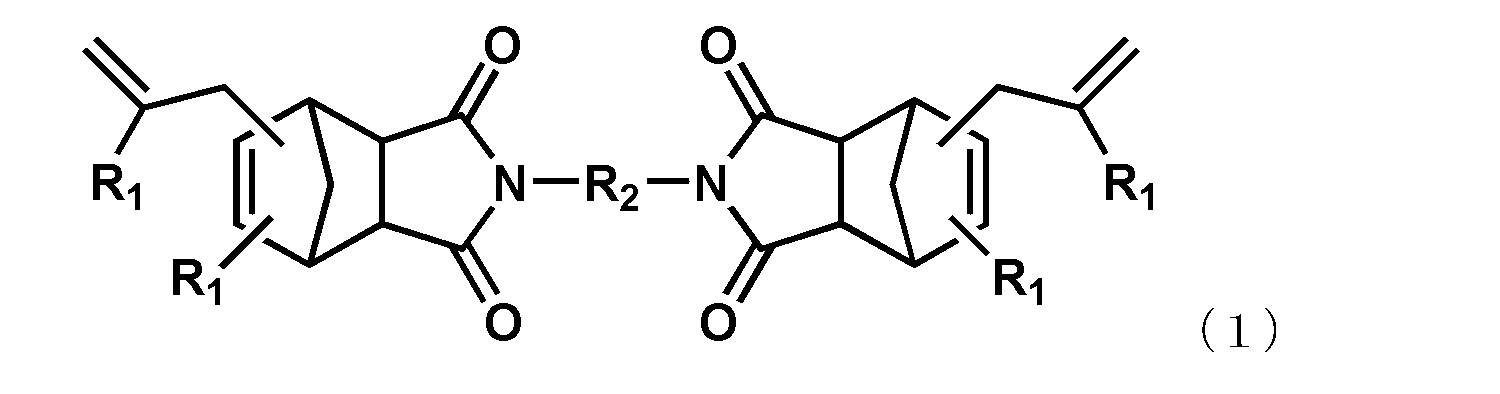
- the alkenyl-substituted nadiimide (A) used in the present embodiment is not particularly limited as long as it is a compound having one or more alkenyl-substituted nadiimide groups in the molecule. Specific examples thereof include compounds represented by the following general formula (1).
- each R 1 independently represents a hydrogen atom or an alkyl group having 1 to 6 carbon atoms
- R 2 represents an alkylene group having 1 to 6 carbon atoms, a phenylene group, a biphenylene group, a naphthylene group, or the following general formula
- the group represented by Formula (2) or (3) is shown.
- R 3 represents a substituent represented by a methylene group, an isopropylidene group, CO, O, S, or SO 2 .
- R 4 represents an independently selected alkylene group having 1 to 4 carbon atoms or a cycloalkylene group having 5 to 8 carbon atoms.
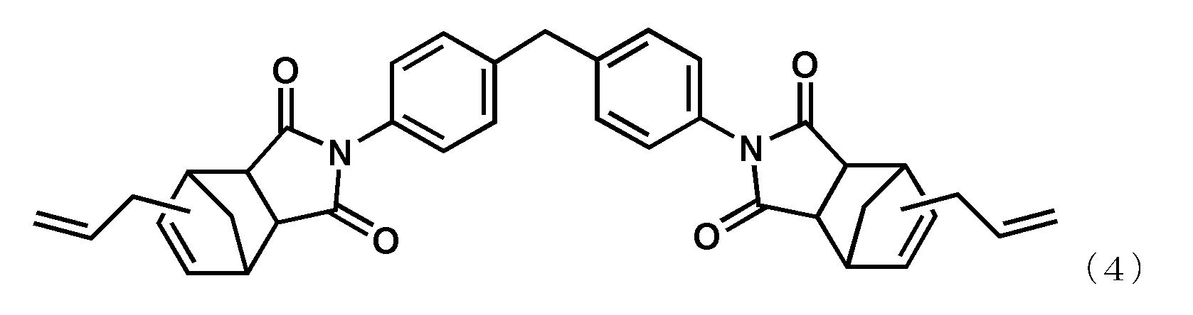
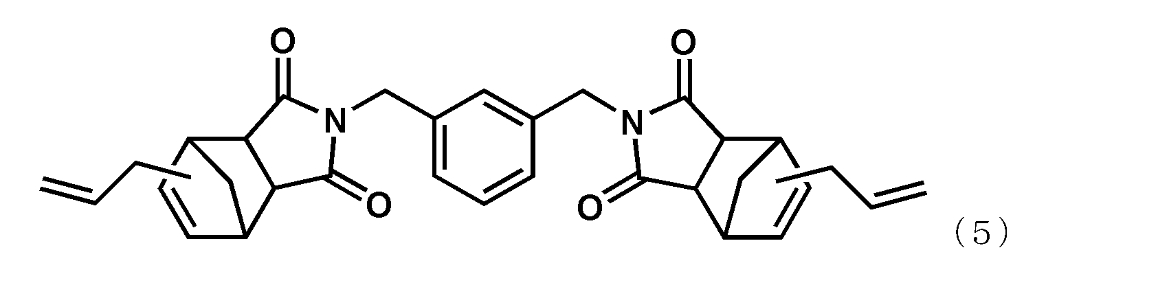
- alkenyl substituted nadiimide (A) represented by Formula (1) examples include, but are not limited to, compounds represented by the following formula (4) (BANI-M (manufactured by Maruzen Petrochemical Co., Ltd.)) and compounds represented by the following formula (5). (BANI-X (manufactured by Maruzen Petrochemical Co., Ltd.)). These may be used alone or in combination of two or more.
- the content of the alkenyl-substituted nadiimide (A) is the number of functional groups of an alkenyl group that is one of its functional groups and the maleimide group of the maleimide compound (B) as described later.
- the ratio is preferably 25 to 45 parts by mass with respect to 100 parts by mass in total of the components (A) to (C) of the resin composition.
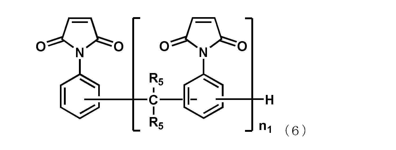
- the maleimide compound (B) used in the present embodiment is not particularly limited as long as it is a compound having one or more maleimide groups in the molecule.
- Specific examples thereof include N-phenylmaleimide, N-hydroxyphenylmaleimide, bis (4-maleimidophenyl) methane, 2,2-bis ⁇ 4- (4-maleimidophenoxy) -phenyl ⁇ propane, bis (3,5 -Dimethyl-4-maleimidophenyl) methane, bis (3-ethyl-5-methyl-4-maleimidophenyl) methane, bis (3,5-diethyl-4-maleimidophenyl) methane, represented by the following formula (6)
- Maleimide compounds, prepolymers of these maleimide compounds, or prepolymers of maleimide compounds and amine compounds may be used alone or in combination of two or more.
- a maleimide compound represented by the formula (6) is preferable, and a maleimide compound represented by the following general formula (6) is particularly preferable.
- R 5 each independently represents a hydrogen atom or a methyl group, and among them, a hydrogen atom is preferable.
- n 1 represents an integer of 1 or more.
- the upper limit value of n 1 is preferably 10, more preferably 7.
- the content of the maleimide compound (B) is such that the number of alkenyl groups ( ⁇ ), which is one of the functional groups of the alkenyl-substituted nadiimide (A), and the maleimide compound (B) as described later. ) Is determined by the ratio of the number of functional groups to the number of maleimide groups ( ⁇ ) ([ ⁇ / ⁇ ]), but is 45 to 70 masses with respect to 100 mass parts in total of the components (A) to (C) of the resin composition. Part. By setting the content of the component (B) in such a range, a printed wiring board having excellent moldability even when filled with a filler and excellent in curability, thermal elastic modulus, desmear resistance, and chemical resistance is obtained. Can do.
- the contents of the alkenyl-substituted nadiimide (A) and the maleimide compound (B) are defined by the ratio of the number of functional groups specified for each.
- the functional group of the alkenyl-substituted nadiimide (A) specified here is an alkenyl group bonded to the molecular end, and the functional group of the maleimide compound (B) is a maleimide group.
- the ratio ([ ⁇ / ⁇ ]) of the number of alkenyl groups ( ⁇ ) of the alkenyl-substituted nadiimide (A) to the number of maleimide groups ( ⁇ ) of the maleimide compound (B) is 0. It is preferably 0.9 to 4.3, and more preferably 1.5 to 4.0.
- the ratio of the functional group ([ ⁇ / ⁇ ]) in such a range it is excellent in low thermal expansion, thermal elastic modulus, heat resistance, moisture absorption heat resistance, desmear resistance, chemical resistance, and easy curability.
- a printed wiring board can be obtained.
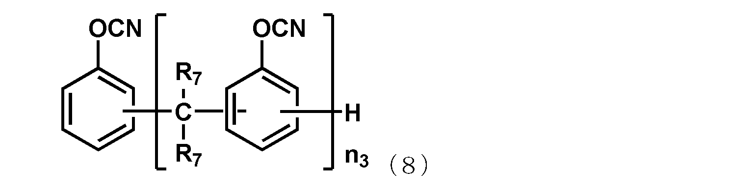
- cyanate ester compound (C) used for this embodiment,
- the novolak represented by following General formula (8) Type cyanate ester, biphenylaralkyl type cyanate ester, bis (3,3-dimethyl-4-cyanatophenyl) methane, bis (4-cyanatophenyl) methane, 1,3-dicyanatobenzene, 1,4- Dicyanatobenzene, 1,3,5-tricyanatobenzene, 1,3-dicyanatonaphthalene, 1,4-dicyanatonaphthalene, 1,6-dicyanatonaphthalene, 1,8-dicyanatonaphthalene, 2,6- Dicyanatonaphthalene, 2,7-dicyanatonaphthalene, 1,3,6-tricyanatonaphthalene, 4,4'-dicyanato Phenyl, bis (4-cyana
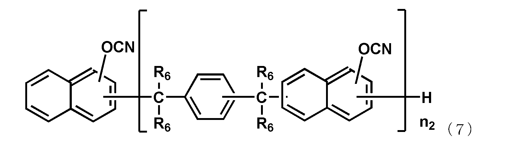
- the naphthol aralkyl cyanate ester compound represented by the following general formula (7), the novolac cyanate ester and the biphenyl aralkyl cyanate ester represented by the following general formula (8) are excellent in flame retardancy and cured. It is particularly preferable because of its high properties and a low thermal expansion coefficient of the cured product.
- each R 6 independently represents a hydrogen atom or a methyl group, and among them, a hydrogen atom is preferable.
- n 2 is an integer of 1 or more.
- the upper limit value of n 2 is preferably 10, more preferably 6.
- R 7 each independently represents a hydrogen atom or a methyl group, and among them, a hydrogen atom is preferable.
- n 3 is an integer of 1 or more.
- the upper limit value of n 3 is preferably 10, more preferably 7.
- cyanate ester compounds are not particularly limited, and any existing method as a cyanate ester synthesis method may be used. Specifically, it can be obtained by reacting a naphthol aralkyl type phenol resin represented by the following general formula (9) with cyanogen halide in an inert organic solvent in the presence of a basic compound. Alternatively, a similar naphthol aralkyl type phenol resin and a salt of a basic compound may be formed in a solution containing water, and then a two-phase interface reaction with cyanogen halide may be performed for synthesis. it can.
- each R 8 independently represents a hydrogen atom or a methyl group, and among them, a hydrogen atom is preferable.
- n 4 represents an integer of 1 or more.
- upper limit of n 4 is preferably 10, more preferably 6.
- the naphthol aralkyl cyanate ester compounds include naphthols such as ⁇ -naphthol and ⁇ -naphthol, p-xylylene glycol, ⁇ , ⁇ '-dimethoxy-p-xylene, 1,4-di (2-hydroxy- It can be selected from those obtained by condensing naphthol aralkyl resin obtained by reaction with 2-propyl) benzene and cyanic acid.
- the content of the cyanate ester compound (C) is 5 to 15 parts by mass with respect to 100 parts by mass in total of the components (A) to (C). preferable.
- resin composition used for the insulating layer of this embodiment other resins can be added in addition to the components (A) to (C) as long as the desired characteristics are not impaired.
- resin such as an epoxy resin, a benzoxazine compound, a phenol resin, and a thermoplastic resin, is mentioned.
- the inorganic filler (D) used in the present embodiment is not particularly limited as long as it has insulating properties.
- silica from the viewpoint of low thermal expansion
- alumina or aluminum nitride from the viewpoint of high thermal conductivity
- the content of the inorganic filler (D) is not particularly limited, but is 100 to 1000 parts by mass with respect to 100 parts by mass in total of the components (A) to (C). It is preferable from the viewpoint of characteristics such as low thermal expansion and high thermal conductivity, and among these, 200 to 800 parts by mass is particularly preferable.
- a silane coupling agent or a wetting and dispersing agent can be used in combination in order to improve the dispersibility of the fine particles and the adhesive strength between the resin and the fine particles or the glass cloth.
- These silane coupling agents are not particularly limited as long as they are silane coupling agents generally used for inorganic surface treatment.
- aminosilanes such as ⁇ -aminopropyltriethoxysilane, N- ⁇ - (aminoethyl) - ⁇ -aminopropyltrimethoxysilane, epoxysilanes such as ⁇ -glycidoxypropyltrimethoxysilane, ⁇ -Acrylic silanes such as acryloxypropyltrimethoxysilane, cationic silanes such as N- ⁇ - (N-vinylbenzylaminoethyl) - ⁇ -aminopropyltrimethoxysilane hydrochloride, phenylsilanes, etc. It is also possible to use one kind or a combination of two or more kinds as appropriate.
- the wetting and dispersing agent is not particularly limited as long as it is a dispersion stabilizer used for coatings.
- wetting and dispersing agents such as DISPER-110, 111, 118, 180, 161, BYK-W996, W9010, W903 manufactured by Big Chemie Japan Co., Ltd. may be mentioned.
- a curing accelerator can be used in combination as long as the desired characteristics are not impaired.
- organic peroxides exemplified by benzoyl peroxide, lauroyl peroxide, acetyl peroxide, parachlorobenzoyl peroxide, di-tert-butyl-diperphthalate, etc .
- azo compounds such as azobisnitrile; N, N-dimethylbenzylamine, N, N-dimethylaniline, N, N-dimethyltoluidine, 2-N-ethylanilinoethanol, tri-n-butylamine, pyridine, quinoline, N-methylmorpholine, triethanolamine, triethylenediamine , Tetramethylbutanediamine, tertiary amines such as N-methylpiperidine; phenols, xylenol, cresol, resorcin, catechol and other phenols; lead nap
- the resin composition used for the insulating layer of the present embodiment may contain a solvent as necessary.
- a solvent for example, when an organic solvent is used, the viscosity at the time of preparing the resin composition is lowered, the handling property is improved, and the impregnation property to the glass cloth is enhanced.
- the kind of solvent will not be specifically limited if it can melt
- Specific examples thereof include ketones such as acetone, methyl ethyl ketone and methyl cellosolve, aromatic hydrocarbons such as toluene and xylene, amides such as dimethylformamide, propylene glycol monomethyl ether and acetate thereof.
- a solvent can be used individually by 1 type or in combination of 2 or more types.
- the resin composition used for the insulating layer of this embodiment can be prepared according to a conventional method. For example, a method for obtaining a resin composition uniformly containing the alkenyl-substituted nadiimide (A), maleimide compound (B), cyanate ester resin (C) and inorganic filler (D) and the other optional components described above. Is preferred. Specifically, for example, the alkenyl-substituted nadiimide (A), the maleimide compound (B), the cyanate ester resin (C), and the inorganic filler (D) are sequentially blended in a solvent and sufficiently stirred in this embodiment.
- the resin composition used for the insulating layer can be easily prepared.
- an organic solvent can be used as necessary.
- the kind of the organic solvent is not particularly limited as long as it can dissolve the resin in the resin composition. Specific examples thereof are as described above.
- the insulating layer of this embodiment may be a prepreg in which a resin composition is impregnated or coated on a base material.
- the prepreg can be obtained, for example, by combining the resin composition with a base material, specifically, impregnating or coating the base material with the resin composition.
- the method for producing the prepreg can be performed according to a conventional method, and is not particularly limited. For example, after impregnating or coating the above-mentioned resin composition on a base material, it is semi-cured (B stage) by heating in a dryer at 100 to 200 ° C. for 1 to 30 minutes. Can be created.
- the amount of the resin composition (including the inorganic filler) relative to the total amount of the prepreg is not particularly limited, but is preferably in the range of 30 to 90% by mass.
- the base material used in the prepreg is not particularly limited, and known materials used for various printed wiring board materials can be appropriately selected and used depending on the intended use and performance. Specific examples thereof include glass fibers such as E glass, D glass, S glass, Q glass, spherical glass, NE glass and T glass, inorganic fibers other than glass such as quartz, polyparaphenylene terephthalamide (Kevlar), and the like.
- E glass cloth, T glass cloth, S glass cloth, Q glass cloth and organic fiber are preferable from the viewpoint of low thermal expansion.
- These base materials can be used alone or in combination of two or more.
- a shape of a base material For example, a woven fabric, a nonwoven fabric, roving, a chopped strand mat, a surfacing mat, etc. are mentioned.
- the weaving method of the woven fabric is not particularly limited, and for example, plain weave, Nanako weave, twill weave and the like are known, and can be appropriately selected from these known ones depending on the intended use and performance. .
- a glass woven fabric whose surface is treated with a fiber-opening treatment or a silane coupling agent is preferably used.
- the thickness and mass of the base material are not particularly limited, but usually about 0.01 to 0.3 mm is preferably used.
- the base material is preferably a glass woven fabric having a thickness of 200 ⁇ m or less and a mass of 250 g / m 2 or less, and a glass woven fabric made of glass fibers of E glass, S glass, and T glass. More preferred.
- the insulating layer of this embodiment may be a laminate obtained by stacking and curing one or more prepregs, or a metal foil-clad laminate obtained by laminating and curing a prepreg and a metal foil.
- the metal foil-clad laminate can be obtained, for example, by stacking at least one prepreg as described above, and laminating and forming the metal foil on one or both sides thereof. Specifically, one or a plurality of the above prepregs are stacked, and if desired, a metal foil such as copper or aluminum is disposed on one or both sides of the prepreg, if desired, by laminating and forming, A metal foil-clad laminate can be created.
- the metal foil used here will not be specifically limited if it is used for printed wiring board material, Well-known copper foils, such as a rolled copper foil and an electrolytic copper foil, are preferable.
- the thickness of the metal foil is not particularly limited, but is preferably 1 to 70 ⁇ m, more preferably 1.5 to 35 ⁇ m.
- a multi-stage press, a multi-stage vacuum press, a continuous molding machine, an autoclave molding machine, etc. can be used at the time of forming a metal foil-clad laminate.
- the temperature is generally 100 to 300 ° C.
- the pressure is 2 to 100 kgf / cm 2
- the heating time is generally 0.05 to 5 hours.
- post-curing can be performed at a temperature of 150 to 300 ° C., if necessary.
- a multilayer board can be formed by laminating and combining the above-described prepreg and a separately prepared wiring board for an inner layer.
- the metal foil-clad laminate can be suitably used as a printed wiring board by forming a predetermined wiring pattern.
- the above metal foil-clad laminate has a low coefficient of thermal expansion, good moldability and chemical resistance, and is particularly effectively used as a printed wiring board for semiconductor packages that require such performance. Can do.
- the insulating layer of the present embodiment can be used as a form of an embedded sheet in which a resin composition is applied to a metal foil or a film in addition to the form of the prepreg described above.
- the insulating layer of the present embodiment may be a resin sheet in which the resin composition is applied to one side or both sides of the support.
- the resin sheet is used as one means of thinning, and for example, a thermosetting resin (including an inorganic filler) used for a prepreg or the like is directly applied to a support such as a metal foil or a film. And can be produced by drying.
- the support used in the production of the resin sheet is not particularly limited, and known materials used for various printed wiring board materials can be used. Examples thereof include a polyimide film, a polyamide film, a polyester film, a polyethylene terephthalate (PET) film, a polybutylene terephthalate (PBT) film, a polypropylene (PP) film, a polyethylene (PE) film, an aluminum foil, a copper foil, and a gold foil. Among these, electrolytic copper foil and PET film are preferable.
- the resin sheet is semi-cured after the resin composition containing the alkenyl-substituted nadiimide (A), maleimide compound (B), cyanate ester compound (C) and inorganic filler (D) described above is applied to the support. It is preferable that it is (B-staged).
- the method for producing the resin sheet is preferably a method for producing a composite of a B-stage resin and a support. Specifically, for example, the resin composition is coated on a support such as a copper foil, and then semi-cured by a method of heating in a dryer at 100 to 200 ° C. for 1 to 60 minutes to produce a resin sheet. The method of doing is mentioned.
- the amount of the resin composition attached to the support is preferably in the range of 1 to 300 ⁇ m in terms of the resin thickness of the resin sheet.
- the insulating layer of this embodiment may be a laminate obtained by stacking and curing one or more resin sheets, or a metal foil-clad laminate obtained by laminating and curing a resin sheet and a metal foil.
- the metal foil-clad laminate can be obtained, for example, by using the above-described resin sheet and arranging the metal foil on one side or both sides and laminating it. For example, a single resin sheet as described above or a plurality of sheets with the support peeled off as desired are stacked, and a metal foil such as copper or aluminum is arranged on one or both sides, and this is laminated as required. By doing so, a metal foil-clad laminate can be produced.
- the metal foil used here will not be specifically limited if it is used for printed wiring board material, Well-known copper foils, such as a rolled copper foil and an electrolytic copper foil, are preferable.
- the method for forming the metal foil-clad laminate and the molding conditions thereof There are no particular limitations on the method for forming the metal foil-clad laminate and the molding conditions thereof, and general methods and conditions for a laminate for a printed wiring board and a multilayer board can be applied.
- a multi-stage press, a multi-stage vacuum press, a continuous molding machine, an autoclave molding machine, etc. can be used at the time of forming a metal foil-clad laminate.
- the temperature is generally 100 to 300 ° C.
- the pressure is 2 to 100 kgf / cm 2
- the heating time is generally 0.05 to 5 hours.
- post-curing can be performed at a temperature of 150 to 300 ° C., if necessary.
- the resin sheet can be used as a build-up material for printed wiring boards.
- the insulating layer of the present embodiment may be a laminate obtained by stacking and curing one or more resin sheets and prepregs, respectively, and laminating and curing a resin sheet, a prepreg, and a metal foil. The resulting metal foil-clad laminate may be used.
- an electroless plating technique can be used when forming a printed wiring board by forming a conductor layer to be a circuit.
- the printed wiring board of the present embodiment is a printed wiring board using the above-described insulating layer, and is, for example, a printed wiring board including the above-described insulating layer and a conductor layer formed on the surface of the insulating layer. Is preferred.
- the printed wiring board of the present embodiment is produced, for example, by forming a conductive layer that becomes a circuit on the above-described insulating layer by metal foil or electroless plating.
- the conductor layer is generally made of copper or aluminum.
- the insulating layer for printed wiring board on which the conductor layer is formed can be suitably used for a printed wiring board by forming a predetermined wiring pattern.
- the printed wiring board of the present embodiment effectively suppresses the warp of the semiconductor plastic package by maintaining the excellent elastic modulus even under the reflow temperature at the time of semiconductor mounting. It can be used particularly effectively as a printed wiring board.
- the printed wiring board of the present embodiment can be manufactured by the following method, for example.
- the metal foil-clad laminate such as a copper-clad laminate
- An inner layer circuit is formed by etching the surface of the metal foil-clad laminate to produce an inner layer substrate. If necessary, surface treatment is performed on the inner layer circuit surface of the inner layer substrate to increase the adhesive strength, then the required number of the prepregs are stacked on the inner layer circuit surface, and a metal foil for the outer layer circuit is laminated on the outer side. Then, it is integrally molded by heating and pressing.
- a multilayer laminate is produced in which an insulating layer made of a cured material of the base material and the thermosetting resin composition is formed between the inner layer circuit and the metal foil for the outer layer circuit.
- desmear treatment is performed to remove smears, which are resin residues derived from the resin component contained in the cured product layer.
- a plated metal film is formed on the wall surface of this hole to connect the inner layer circuit and the metal foil for the outer layer circuit, and the outer layer circuit is formed by etching the metal foil for the outer layer circuit to produce a printed wiring board. Is done.
- the above-described prepreg (the base material and the above-described resin composition attached thereto) and the metal foil-clad laminate resin composition layer (the layer made of the above-described resin composition) include the above-described resin composition.
- An insulating layer is formed.
- Example 1 ⁇ -naphthol aralkyl type cyanate ester resin (Mitsubishi Gas Chemical Co., Ltd.) 10 parts by mass, maleimide compound (BMI-2300, manufactured by Daiwa Kasei Kogyo Co., Ltd.) 55 parts by mass and bisallyl nadiimide (BANI-M, 35 parts by mass of Maruzen Petrochemical Co., Ltd.) and 150 parts by mass of slurry silica (SC-5050MOB, 1.5 ⁇ m, manufactured by Admatex Co., Ltd.), wetting and dispersing agent (DISPERBYK-161, manufactured by Big Chemie Japan Co., Ltd.) 1 part by mass and 1 part of a silane coupling agent (Z6040, manufactured by Toray Dow Corning Co., Ltd.) were mixed and diluted with methyl ethyl ketone to obtain a varnish.
- maleimide compound BMI-2300, manufactured by Daiwa Kasei Kogyo Co., Ltd.
- [ ⁇ / ⁇ ] (parts by mass of (B) / functional group equivalent of (B)) / (parts by mass of (A) / functional group equivalent of (A))
- the obtained prepreg had no glass transition temperature (Tg) in the region of 400 ° C. or lower.
- Example 2 10 parts by mass of ⁇ -naphthol aralkyl-type cyanate ester resin (manufactured by Mitsubishi Gas Chemical Co., Inc.), 65 parts by mass of maleimide compound (BMI-2300, manufactured by Daiwa Kasei Kogyo Co., Ltd.) and bisallyl nadiimide (BANI-M, 25 parts by mass of Maruzen Petrochemical Co., Ltd.) and 150 parts by mass of slurry silica (SC-5050MOB, 1.5 ⁇ m, manufactured by Admatex Co., Ltd.), wetting and dispersing agent (DISPERBYK-161, manufactured by Big Chemie Japan Co., Ltd.) 1 part by mass and 1 part of a silane coupling agent (Z6040, manufactured by Toray Dow Corning Co., Ltd.) were mixed and diluted with methyl ethyl ketone to obtain a varnish.
- ⁇ -naphthol aralkyl-type cyanate ester resin manufactured
- This varnish was impregnated and applied to an E glass woven fabric and dried by heating at 160 ° C. for 3 minutes to obtain a prepreg having a resin composition content of 46% by mass.
- [ ⁇ / ⁇ ] represented by the ratio of the number of alkenyl groups ( ⁇ ) of the alkenyl-substituted nadiimide (A) to the number of maleimide groups ( ⁇ ) of the maleimide compound (B) was 4.00.
- the obtained prepreg had no glass transition temperature (Tg) in the region of 400 ° C. or lower.
- This varnish was impregnated and applied to an E glass woven fabric and dried by heating at 160 ° C. for 3 minutes to obtain a prepreg having a resin composition content of 46% by mass.
- [ ⁇ / ⁇ ] represented by the ratio of the number of alkenyl groups ( ⁇ ) of the alkenyl-substituted nadiimide (A) to the number of maleimide groups ( ⁇ ) of the maleimide compound (B) was 6.15.
- Table 1 shows the results of measuring the linear thermal expansion coefficient and the flexural modulus using the obtained copper-clad laminate.
- Bending elastic modulus Using a sample of 50 mm ⁇ 25 mm ⁇ 0.8 mm, measurement was carried out at 25 ° C. and 250 ° C. respectively with an autograph (AG-Xplus manufactured by Shimadzu Corporation) according to JIS standard C6481. .
- Elastic modulus loss rate The difference between the flexural modulus (a) at 25 ° C. measured by the above method and the elastic modulus (b) of the flexural modulus at 250 ° C. was calculated by the following formula.
- Elastic modulus loss rate ⁇ (a)-(b) ⁇ / (a) ⁇ 100
- Warpage evaluation The amount of warpage of the substrate was evaluated using Thermoray PS200L shadow moire analysis manufactured by AKROMETRIX.
- the sample size of the substrate was 40 mm ⁇ 40 mm, and the measurement area was 36 mm ⁇ 36 mm.
- the sample of the substrate was heated from room temperature to 260 ° C., and then the amount of warpage when cooled to 50 ° C. was measured.
- a case where the warpage was improved by 15% or more with respect to Comparative Example 1 was evaluated as ⁇ , and a case where the warpage was improved by 5% or more and less than 15% was determined as ⁇ .
- Synthesis Example 1 Synthesis of ⁇ -naphthol aralkyl-type cyanate ester resin A reactor equipped with a thermometer, a stirrer, a dropping funnel and a reflux condenser was cooled in advance to 0 to 5 ° C. with brine, and then cyan chloride 7 .47 g (0.122 mol), 35% hydrochloric acid 9.75 g (0.0935 mol), water 76 ml, and methylene chloride 44 ml were charged.
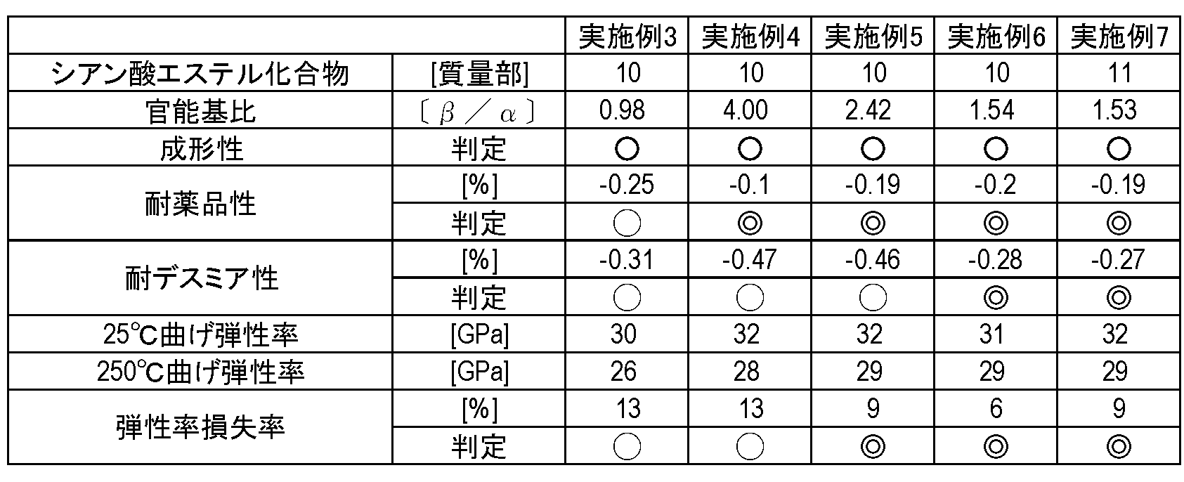
- Example 3 10 parts by mass of the ⁇ -naphthol aralkyl-type cyanate ester resin (cyanate equivalent: 261 g / eq.) Obtained in Synthesis Example 1, all R 5 in formula (6) are hydrogen atoms, and n 1 is 1 to 3.
- a certain maleimide compound (BMI-2300, manufactured by Daiwa Kasei Kogyo Co., Ltd.), 55 parts by mass of an alkenyl-substituted nadiimide compound represented by the formula (4) (BANI-M, manufactured by Maruzen Petrochemical Co., Ltd.), slurry 100 parts by mass of silica (SC-5050MOB, average particle size: 1.5 ⁇ m, manufactured by Admatex Co., Ltd.), 1 part by mass of a wetting dispersant (DISPERBYK-161, manufactured by Big Chemie Japan Co., Ltd.), a silane coupling agent Varnish was obtained by mixing 5 parts by mass (Z6040, manufactured by Toray Dow Corning Co., Ltd.).
- This varnish was diluted with methyl ethyl ketone, impregnated and applied to E glass woven fabric, and heated and dried at 140 ° C. for 3 minutes to obtain a prepreg having a resin composition content of 44 mass%.
- [ ⁇ / ⁇ ] represented by the ratio of the number of alkenyl groups ( ⁇ ) of the alkenyl-substituted nadiimide (A) to the number of maleimide groups ( ⁇ ) of the maleimide compound (B) was 0.98.
- [ ⁇ / ⁇ ] is expressed by the following calculation formula.
- [ ⁇ / ⁇ ] (parts by mass of (B) / functional group equivalent of (B)) / (parts by mass of (A) / functional group equivalent of (A))
- the obtained prepreg had no glass transition temperature (Tg) in the region of 400 ° C. or lower.
- Example 4 A prepreg was obtained in the same manner as in Example 3, except that the maleimide compound (BMI-2300) and the alkenyl-substituted nadiimide (BANI-M) used in Example 3 were changed to 65 parts by mass and 25 parts by mass, respectively.
- [ ⁇ / ⁇ ] represented by the ratio of the number of alkenyl groups ( ⁇ ) of the alkenyl-substituted nadiimide (A) to the number of maleimide groups ( ⁇ ) of the maleimide compound (B) was 4.00.
- the obtained prepreg had no glass transition temperature (Tg) in the region of 400 ° C. or lower.
- Example 5 A prepreg was obtained in the same manner as in Example 3, except that the maleimide compound (BMI-2300) and alkenyl-substituted nadiimide (BANI-M) used in Example 3 were changed to 55 parts by mass and 35 parts by mass, respectively.
- [ ⁇ / ⁇ ] represented by the ratio of the number of alkenyl groups ( ⁇ ) of the alkenyl-substituted nadiimide (A) to the number of maleimide groups ( ⁇ ) of the maleimide compound (B) was 2.42.
- the obtained prepreg had no glass transition temperature (Tg) in the region of 400 ° C. or lower.
- Example 6 A prepreg was obtained in the same manner as in Example 3 except that the maleimide compound (BMI-2300) and alkenyl-substituted nadiimide (BANI-M) used in Example 3 were changed to 45 parts by mass and 45 parts by mass, respectively.
- [b / a] represented by the ratio of the number of alkenyl groups (a) of the alkenyl-substituted nadiimide (A) to the number of maleimide groups (b) of the maleimide compound (B) was 1.54.
- the obtained prepreg had no glass transition temperature (Tg) in the region of 400 ° C. or lower.
- Example 7 The ⁇ -naphthol aralkyl type cyanate ester resin used in Example 3 was 11 parts by mass, the maleimide compound (BMI-2300) was 47 parts by mass, and the alkenyl-substituted nadiimide compound (BANI-M) represented by the formula (4)
- a prepreg was obtained in the same manner as in Example 3 except that 42 parts by mass of an alkenyl-substituted nadiimide compound represented by formula (5) (BANI-X, manufactured by Maruzen Petrochemical Co., Ltd.) was used instead of
- [ ⁇ / ⁇ ] represented by the ratio of the number of alkenyl groups ( ⁇ ) of the alkenyl-substituted nadiimide (A) to the number of maleimide groups ( ⁇ ) of the maleimide compound (B) was 1.53.
- the obtained prepreg had no glass transition temperature (Tg) in the region of 400 ° C. or lower.
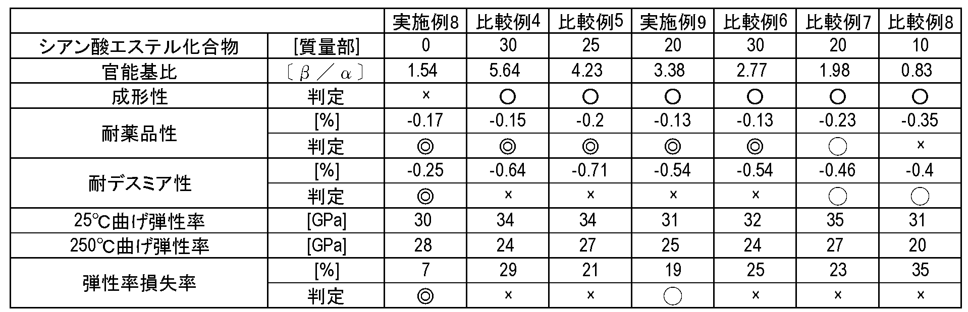
- Example 8 The procedure was carried out except that the ⁇ -naphthol aralkyl type cyanate ester resin used in Example 3 was not used and the maleimide compound (BMI-2300) and the alkenyl-substituted nadiimide (BANI-M) were respectively 50 parts by mass and 50 parts by mass.
- a prepreg was obtained in the same manner as in Example 3.
- [ ⁇ / ⁇ ] represented by the ratio of the number of alkenyl groups ( ⁇ ) of the alkenyl-substituted nadiimide (A) to the number of maleimide groups ( ⁇ ) of the maleimide compound (B) was 1.54.
- the obtained prepreg had no glass transition temperature (Tg) in the region of 400 ° C. or lower.
- Comparative Example 5 Except for 25 parts by mass of ⁇ -naphthol aralkyl-type cyanate ester resin used in Example 3 and 55 parts by mass and 20 parts by mass of maleimide compound (BMI-2300) and alkenyl-substituted nadiimide (BANI-M), respectively.
- a prepreg was obtained in the same manner as in Example 3.
- [ ⁇ / ⁇ ] represented by the ratio of the number of alkenyl groups ( ⁇ ) of the alkenyl-substituted nadiimide (A) to the number of maleimide groups ( ⁇ ) of the maleimide compound (B) was 4.23.
- Example 9 Example except that ⁇ -naphthol aralkyl type cyanate ester resin used in Example 3 was changed to 20 parts by mass maleimide compound (BMI-2300) and alkenyl-substituted nadiimide (BANI-M) to 55 parts by mass and 25 parts by mass, respectively.
- BMI-2300 alkenyl-substituted nadiimide
- BANI-M alkenyl-substituted nadiimide
- Comparative Example 6 Except for 30 parts by mass of ⁇ -naphthol aralkyl-type cyanate ester resin used in Example 3, and 45 parts by mass and 25 parts by mass of maleimide compound (BMI-2300) and alkenyl-substituted nadiimide (BANI-M), respectively.
- a prepreg was obtained in the same manner as in Example 3.
- [ ⁇ / ⁇ ] represented by the ratio of the number of alkenyl groups ( ⁇ ) of the alkenyl-substituted nadiimide (A) to the number of maleimide groups ( ⁇ ) of the maleimide compound (B) was 2.77.
- Comparative Example 7 Except that 20 parts by mass of ⁇ -naphthol aralkyl-type cyanate ester resin used in Example 3 and 45 parts by mass and 35 parts by mass of maleimide compound (BMI-2300) and alkenyl-substituted nadiimide (BANI-M) were used. A prepreg was obtained in the same manner as in Example 3. At this time, [ ⁇ / ⁇ ] represented by the ratio of the number of alkenyl groups ( ⁇ ) of the alkenyl-substituted nadiimide (A) to the number of maleimide groups ( ⁇ ) of the maleimide compound (B) was 1.98.
- Comparative Example 8 Except that 10 parts by mass of ⁇ -naphthol aralkyl type cyanate ester resin used in Example 3 and 35 parts by mass and 65 parts by mass of maleimide compound (BMI-2300) and alkenyl-substituted nadiimide (BANI-M) were used. A prepreg was obtained in the same manner as in Example 3. At this time, [ ⁇ / ⁇ ] represented by the ratio of the number of alkenyl groups ( ⁇ ) of the alkenyl-substituted nadiimide (A) to the number of maleimide groups ( ⁇ ) of the maleimide compound (B) was 0.83.
- Tables 2 and 3 show the results of evaluation of formability, chemical resistance, desmear resistance, and flexural modulus using the obtained copper-clad laminate.
- Method for evaluating physical properties of metal foil-clad laminate Formability After removing the copper foil of the copper-clad laminate by etching, the surface was observed and the presence or absence of voids was evaluated.
- Desmear resistance To evaluate the chemical resistance in the desmear process, after removing the copper foil of the copper-clad laminate by etching, the swelling liquid is 80 in the Swinging Dip Securigant P of Atotech Japan Co., Ltd. Immerse for 10 minutes at °C, then immerse in concentrate compact CP of Atotech Japan Co., Ltd. for 5 minutes at 80 °C as a roughening solution, and finally reduce conditioner securigant P500 of Atotech Japan Co., Ltd. as a neutralizing solution. For 10 minutes at 45 ° C. The mass reduction amount (mass%) after performing this process 3 times was evaluated. Those with a weight reduction rate of -0.3 or less, ⁇ , those with a weight reduction rate of greater than -0.3% and less than -0.5%, and those with a weight reduction rate of greater than -0.5% It described as x.
- Bending elastic modulus Using a sample of 50 mm ⁇ 25 mm ⁇ 0.8 mm, measurement was carried out at 25 ° C. and 250 ° C. respectively with an autograph (AG-Xplus manufactured by Shimadzu Corporation) according to JIS standard C6481. .
- Elastic modulus loss rate The difference between the flexural modulus (a) at 25 ° C. measured by the above method and the elastic modulus (b) of the flexural modulus at 250 ° C. was calculated by the following formula.
- Elastic modulus loss rate [ ⁇ (a)-(b) ⁇ / (a)] ⁇ 100
- the case where the elastic modulus loss rate was greater than 20% was rated as x, the case where the elastic modulus loss rate was 20% to 10%, and the case where the elastic modulus loss rate was less than 10%.
- the present invention it is possible to manufacture a semiconductor plastic package that is less warped due to elements different from the conventional one, and that is excellent in manufacturing yield and reliability.
Landscapes
- Engineering & Computer Science (AREA)
- Chemical & Material Sciences (AREA)
- Microelectronics & Electronic Packaging (AREA)
- Manufacturing & Machinery (AREA)
- Materials Engineering (AREA)
- Organic Chemistry (AREA)
- Health & Medical Sciences (AREA)
- Chemical Kinetics & Catalysis (AREA)
- Medicinal Chemistry (AREA)
- Polymers & Plastics (AREA)
- Inorganic Chemistry (AREA)
- Reinforced Plastic Materials (AREA)
- Laminated Bodies (AREA)
- Compositions Of Macromolecular Compounds (AREA)
- Organic Insulating Materials (AREA)
- Insulating Bodies (AREA)
Abstract
Description
[1]
25℃における曲げ弾性率と250℃における熱時曲げ弾性率との差が20%以下であるプリント配線板用絶縁層。
[2]
前記絶縁層が樹脂組成物を含み、
該樹脂組成物が、アルケニル置換ナジイミド(A)、マレイミド化合物(B)、シアン酸エステル化合物(C)及び無機充填材(D)を含み、該シアン酸エステル化合物(C)の含有量が、成分(A)~(C)の合計100質量部に対して5~15質量部であって、該アルケニル置換ナジイミド(A)のアルケニル基数(α)と該マレイミド化合物(B)のマレイミド基数(β)の比(〔β/α〕)が、0.9~4.3である、[1]に記載のプリント配線板用絶縁層。
[3]
前記アルケニル置換ナジイミド(A)が下記一般式(1)で表される化合物である、[2]に記載のプリント配線板用絶縁層。


[4]
前記アルケニル置換ナジイミド(A)が、下記式(4)及び/又は(5)で表される化合物である、[2]に記載のプリント配線板用絶縁層。


前記マレイミド化合物(B)が、ビス(4-マレイミドフェニル)メタン、2,2-ビス{4-(4-マレイミドフェノキシ)-フェニル}プロパン、ビス(3-エチル-5-メチル-4-マレイミドフェニル)メタン及び下記一般式(6)で表されるマレイミド化合物からなる群より選ばれる少なくとも1種である、[2]~[4]のいずれかに記載のプリント配線板用絶縁層。

[6]
前記シアン酸エステル化合物(C)が、下記一般式(7)及び/又は式(8)で表される化合物である、[2]~[5]のいずれかに記載のプリント配線板用絶縁層。

[7]
前記絶縁層が、樹脂組成物を基材に含浸又は塗布したプリプレグである、[1]~[6]のいずれかに記載のプリント配線板用絶縁層。
[8]
前記基材が、Eガラスクロス、Tガラスクロス、Sガラスクロス、Qガラスクロス及び有機繊維からなる群より選ばれる少なくとも1種である、[7]に記載のプリント配線板用絶縁層。
[9]
前記絶縁層が、樹脂組成物を支持体に塗布したレジンシートである、[1]~[6]のいずれかに記載のプリント配線板用絶縁層。
[10]
前記絶縁層が、レジンシート及びプリプレグからなる群より選ばれる少なくとも1種を1枚以上重ねて硬化して得られる積層板である、[1]~[6]のいずれかに記載のプリント配線板用絶縁層。
[11]
前記絶縁層が、レジンシート及びプリプレグからなる群より選ばれる少なくとも1種と、金属箔とを積層して硬化して得られる金属箔張積層板である、[1]~[6]のいずれかに記載のプリント配線板用絶縁層。
[12]
[1]~[11]のいずれかに記載のプリント配線板用絶縁層を使用したプリント配線板。
[13]
[1]~[11]のいずれかに記載のプリント配線板用絶縁層と、前記絶縁層の表面に形成された導体層とを含むプリント配線板。


α-ナフトールアラルキル型シアン酸エステル樹脂(三菱瓦斯化学(株)製)10質量部、マレイミド化合物(BMI-2300、大和化成工業(株)製)55質量部及びビスアリルナジイミド(BANI-M、丸善石油化学(株)製)35質量部にスラリーシリカ(SC-5050MOB、1.5μm、アドマテックス(株)製)150質量部、湿潤分散剤(DISPERBYK-161、ビックケミージャパン(株)製)1質量部、シランカップリング剤(Z6040、東レ・ダウコーニング(株)製)1部を混合し、メチルエチルケトンで希釈することでワニスを得た。このワニスをEガラス織布に含浸塗工し、160℃で3分間加熱乾燥して、樹脂組成物含有量46質量%のプリプレグを得た。この時アルケニル置換ナジイミド(A)のアルケニル基数(α)とマレイミド化合物(B)のマレイミド基数(β)の比で表される〔β/α〕は、2.42となった。また、〔β/α〕は、下記計算式で表される。
α-ナフトールアラルキル型シアン酸エステル樹脂(三菱瓦斯化学(株)製)10質量部、マレイミド化合物(BMI-2300、大和化成工業(株)製)65質量部及びビスアリルナジイミド(BANI-M、丸善石油化学(株)製)25質量部にスラリーシリカ(SC-5050MOB、1.5μm、アドマテックス(株)製)150質量部、湿潤分散剤(DISPERBYK-161、ビックケミージャパン(株)製)1質量部、シランカップリング剤(Z6040、東レ・ダウコーニング(株)製)1部を混合し、メチルエチルケトンで希釈することでワニスを得た。このワニスをEガラス織布に含浸塗工し、160℃で3分間加熱乾燥して、樹脂組成物含有量46質量%のプリプレグを得た。この時アルケニル置換ナジイミド(A)のアルケニル基数(α)とマレイミド化合物(B)のマレイミド基数(β)の比で表される〔β/α〕は、4.00となった。また、得られたプリプレグは、400℃以下の領域でガラス転移温度(Tg)が無かった。
α-ナフトールアラルキル型シアン酸エステル樹脂(三菱瓦斯化学(株)製)35質量部、マレイミド化合物(BMI-2300、大和化成工業(株)製)30質量部及びナフチレンエーテル型エポキシ樹脂(HP-6000、DIC(株)製)35質量部にスラリーシリカ(SC-5050MOB、1.5μm、アドマテックス(株)製)150質量部、湿潤分散剤(DISPERBYK-161、ビックケミージャパン(株)製)1質量部、シランカップリング剤(Z6040、東レ・ダウコーニング(株)製)1部を混合し、メチルエチルケトンで希釈することでワニスを得た。このワニスをEガラス織布に含浸塗工し、160℃で3分間加熱乾燥して、樹脂組成物含有量46質量%のプリプレグを得た。
α-ナフトールアラルキル型シアン酸エステル樹脂(三菱瓦斯化学(株)製)35質量部、マレイミド化合物(BMI-2300、大和化成工業(株)製)35質量部及びフェノールノボラック型エポキシ樹脂(N-770、DIC(株)製)25質量部、ナフチルメタン型エポキシ樹脂(HP-4710、DIC(株)製)5質量部にスラリーシリカ(SC-5050MOB、1.5μm、アドマテックス(株)製)150質量部、湿潤分散剤(DISPERBYK-161、ビックケミージャパン(株)製)1質量部、シランカップリング剤(Z6040、東レ・ダウコーニング(株)製)1部を混合し、メチルエチルケトンで希釈することでワニスを得た。このワニスをEガラス織布に含浸塗工し、160℃で3分間加熱乾燥して、樹脂組成物含有量46質量%のプリプレグを得た。
α-ナフトールアラルキル型シアン酸エステル樹脂(三菱瓦斯化学(株)製)35質量部、マレイミド化合物(BMI-2300、大和化成工業(株)製)40質量部及びナフチレンエーテル型エポキシ樹脂(HP-4710、DIC(株)製)10質量部、ナフチルメタン型エポキシ樹脂(HP-4710、DIC(株)製)5質量部、ビスアリルナジイミド(BANI-M、丸善石油化学(株)製)10質量部にスラリーシリカ(SC-5050MOB、1.5μm、アドマテックス(株)製)150質量部、湿潤分散剤(DISPERBYK-161、ビックケミージャパン(株)製)1質量部、シランカップリング剤(Z6040、東レ・ダウコーニング(株)製)1部を混合し、メチルエチルケトンで希釈することでワニスを得た。このワニスをEガラス織布に含浸塗工し、160℃で3分間加熱乾燥して、樹脂組成物含有量46質量%のプリプレグを得た。この時アルケニル置換ナジイミド(A)のアルケニル基数(α)とマレイミド化合物(B)のマレイミド基数(β)の比で表される〔β/α〕は、6.15となった。
実施例1~2及び比較例1~3で得られたプリプレグを、それぞれ1枚又は8枚重ねて12μm厚の電解銅箔(3EC-III、三井金属鉱業(株)製)を上下に配置し、圧力30kgf/cm2、温度220℃で120分間の積層成型を行い、絶縁層厚さ0.1mm又は0.8mmの銅張積層板を得た。
線熱膨張係数:銅張積層板の銅箔をエッチングにより除去した後に、熱機械分析装置(TAインスツルメント製)で40℃から340℃まで毎分10℃で昇温し、60℃から120℃での面方向の線熱膨張係数を測定した。測定方向は積層板のガラスクロスの縦方向(Warp)を測定した。

温度計、攪拌器、滴下漏斗及び還流冷却器を取りつけた反応器を予めブラインにより0~5℃に冷却しておき、そこへ塩化シアン7.47g(0.122mol)、35%塩酸9.75g(0.0935mol)、水76ml、及び塩化メチレン44mlを仕込んだ。
合成例1で得られたα-ナフトールアラルキル型シアン酸エステル樹脂(シアネート当量:261g/eq.)10質量部、式(6)におけるR5がすべて水素原子であり、n1が1~3であるマレイミド化合物(BMI-2300、大和化成工業(株)製)35質量部、式(4)で表されるアルケニル置換ナジイミド化合物(BANI-M、丸善石油化学(株)製)55質量部、スラリーシリカ(SC-5050MOB、平均粒子径:1.5μm、アドマテックス(株)製)100質量部、湿潤分散剤(DISPERBYK-161、ビックケミージャパン(株)製)を1質量部、シランカップリング剤(Z6040、東レ・ダウコーニング(株)製)5質量部を混合してワニスを得た。このワニスをメチルエチルケトンで希釈し、Eガラス織布に含浸塗工し、140℃で3分間加熱乾燥して、樹脂組成物含有量44質量%のプリプレグを得た。この時アルケニル置換ナジイミド(A)のアルケニル基数(α)とマレイミド化合物(B)のマレイミド基数(β)の比で表される〔β/α〕は、0.98となった。また、〔β/α〕は、下記計算式で表される。
実施例3で使用したマレイミド化合物(BMI-2300)、アルケニル置換ナジイミド(BANI-M)をそれぞれ65質量部、25質量部とした以外は実施例3と同様にしてプリプレグを得た。この時アルケニル置換ナジイミド(A)のアルケニル基数(α)とマレイミド化合物(B)のマレイミド基数(β)の比で表される〔β/α〕は、4.00となった。また、得られたプリプレグは、400℃以下の領域でガラス転移温度(Tg)が無かった。
実施例3で使用したマレイミド化合物(BMI-2300)、アルケニル置換ナジイミド(BANI-M)をそれぞれ55質量部、35質量部とした以外は実施例3と同様にしてプリプレグを得た。この時アルケニル置換ナジイミド(A)のアルケニル基数(α)とマレイミド化合物(B)のマレイミド基数(β)の比で表される〔β/α〕は、2.42となった。また、得られたプリプレグは、400℃以下の領域でガラス転移温度(Tg)が無かった。
実施例3で使用したマレイミド化合物(BMI-2300)、アルケニル置換ナジイミド(BANI-M)をそれぞれ45質量部、45質量部とした以外は実施例3と同様にしてプリプレグを得た。この時アルケニル置換ナジイミド(A)のアルケニル基数(a)とマレイミド化合物(B)のマレイミド基数(b)の比で表される〔b/a〕は、1.54となった。また、得られたプリプレグは、400℃以下の領域でガラス転移温度(Tg)が無かった。
実施例3で使用したα-ナフトールアラルキル型シアン酸エステル樹脂を11質量部、マレイミド化合物(BMI-2300)を47質量部とし、式(4)で表されるアルケニル置換ナジイミド化合物(BANI-M)の代わりに式(5)で表されるアルケニル置換ナジイミド化合物(BANI-X、丸善石油化学(株)製)を42質量部用いた以外は実施例3と同様にしてプリプレグを得た。この時アルケニル置換ナジイミド(A)のアルケニル基数(α)とマレイミド化合物(B)のマレイミド基数(β)の比で表される〔β/α〕は、1.53となった。また、得られたプリプレグは、400℃以下の領域でガラス転移温度(Tg)が無かった。
実施例3で使用したα-ナフトールアラルキル型シアン酸エステル樹脂を使用せず、マレイミド化合物(BMI-2300)、アルケニル置換ナジイミド(BANI-M)をそれぞれ50質量部、50質量部とした以外は実施例3と同様にしてプリプレグを得た。この時アルケニル置換ナジイミド(A)のアルケニル基数(α)とマレイミド化合物(B)のマレイミド基数(β)の比で表される〔β/α〕は、1.54となった。また、得られたプリプレグは、400℃以下の領域でガラス転移温度(Tg)が無かった。
実施例3で使用したα-ナフトールアラルキル型シアン酸エステル樹脂を30質量部、マレイミド化合物(BMI-2300)、アルケニル置換ナジイミド(BANI-M)をそれぞれ55質量部、15質量部とした以外は実施例3と同様にしてプリプレグを得た。この時アルケニル置換ナジイミド(A)のアルケニル基数(α)とマレイミド化合物(B)のマレイミド基数(β)の比で表される〔β/α〕は、5.64となった。
実施例3で使用したα-ナフトールアラルキル型シアン酸エステル樹脂を25質量部、マレイミド化合物(BMI-2300)、アルケニル置換ナジイミド(BANI-M)をそれぞれ55質量部、20質量部とした以外は実施例3と同様にしてプリプレグを得た。この時アルケニル置換ナジイミド(A)のアルケニル基数(α)とマレイミド化合物(B)のマレイミド基数(β)の比で表される〔β/α〕は、4.23となった。
実施例3で使用したα-ナフトールアラルキル型シアン酸エステル樹脂を20質量部マレイミド化合物(BMI-2300)、アルケニル置換ナジイミド(BANI-M)をそれぞれ55質量部、25質量部とした以外は実施例3と同様にしてプリプレグを得た。この時アルケニル置換ナジイミド(A)のアルケニル基数(α)とマレイミド化合物(B)のマレイミド基数(β)の比で表される〔β/α〕は、3.38となった。また、得られたプリプレグは、400℃以下の領域でガラス転移温度(Tg)が無かった。
実施例3で使用したα-ナフトールアラルキル型シアン酸エステル樹脂を30質量部、マレイミド化合物(BMI-2300)、アルケニル置換ナジイミド(BANI-M)をそれぞれ45質量部、25質量部とした以外は実施例3と同様にしてプリプレグを得た。この時アルケニル置換ナジイミド(A)のアルケニル基数(α)とマレイミド化合物(B)のマレイミド基数(β)の比で表される〔β/α〕は、2.77となった。
実施例3で使用したα-ナフトールアラルキル型シアン酸エステル樹脂を20質量部、マレイミド化合物(BMI-2300)、アルケニル置換ナジイミド(BANI-M)をそれぞれ45質量部、35質量部とした以外は実施例3と同様にしてプリプレグを得た。この時アルケニル置換ナジイミド(A)のアルケニル基数(α)とマレイミド化合物(B)のマレイミド基数(β)の比で表される〔β/α〕は、1.98となった。
実施例3で使用したα-ナフトールアラルキル型シアン酸エステル樹脂を10質量部、マレイミド化合物(BMI-2300)、アルケニル置換ナジイミド(BANI-M)をそれぞれ35質量部、65質量部とした以外は実施例3と同様にしてプリプレグを得た。この時アルケニル置換ナジイミド(A)のアルケニル基数(α)とマレイミド化合物(B)のマレイミド基数(β)の比で表される〔β/α〕は、0.83となった。
実施例3~9及び比較例4~8得られたプリプレグを、それぞれ1枚、4枚、又は8枚重ねて12μm厚の電解銅箔(3EC-III、三井金属鉱業(株)製)を上下に配置し、圧力30kgf/cm2、温度220℃で120分間の積層成型を行い、絶縁層厚さ0.1mm、0.4mm又は0.8mmの銅張積層板を得た。
成形性:銅張積層板の銅箔をエッチングにより除去したのちに、表面を観察しボイドの有無を評価した。
Claims (13)
- 25℃における曲げ弾性率と250℃における熱時曲げ弾性率との差が20%以下であるプリント配線板用絶縁層。
- 前記絶縁層が樹脂組成物を含み、
該樹脂組成物が、アルケニル置換ナジイミド(A)、マレイミド化合物(B)、シアン酸エステル化合物(C)及び無機充填材(D)を含み、該シアン酸エステル化合物(C)の含有量が、成分(A)~(C)の合計100質量部に対して5~15質量部であって、該アルケニル置換ナジイミド(A)のアルケニル基数(α)と該マレイミド化合物(B)のマレイミド基数(β)の比(〔β/α〕)が、0.9~4.3である、請求項1に記載のプリント配線板用絶縁層。 - 前記アルケニル置換ナジイミド(A)が下記一般式(1)で表される化合物である、請求項2に記載のプリント配線板用絶縁層。


- 前記アルケニル置換ナジイミド(A)が、下記式(4)及び/又は(5)で表される化合物である、請求項2に記載のプリント配線板用絶縁層。

- 前記マレイミド化合物(B)が、ビス(4-マレイミドフェニル)メタン、2,2-ビス{4-(4-マレイミドフェノキシ)-フェニル}プロパン、ビス(3-エチル-5-メチル-4-マレイミドフェニル)メタン及び下記一般式(6)で表されるマレイミド化合物からなる群より選ばれる少なくとも1種である、請求項2~4のいずれか一項に記載のプリント配線板用絶縁層。
- 前記シアン酸エステル化合物(C)が、下記一般式(7)及び/又は式(8)で表される化合物である、請求項2~5のいずれか一項に記載のプリント配線板用絶縁層。

- 前記絶縁層が、樹脂組成物を基材に含浸又は塗布したプリプレグである、請求項1~6のいずれか一項に記載のプリント配線板用絶縁層。
- 前記基材が、Eガラスクロス、Tガラスクロス、Sガラスクロス、Qガラスクロス及び有機繊維からなる群より選ばれる少なくとも1種である、請求項7に記載のプリント配線板用絶縁層。
- 前記絶縁層が、樹脂組成物を支持体に塗布したレジンシートである、請求項1~6のいずれか一項に記載のプリント配線板用絶縁層。
- 前記絶縁層が、レジンシート及びプリプレグからなる群より選ばれる少なくとも1種を1枚以上重ねて硬化して得られる積層板である、請求項1~6のいずれか一項に記載のプリント配線板用絶縁層。
- 前記絶縁層が、レジンシート及びプリプレグからなる群より選ばれる少なくとも1種と、金属箔とを積層して硬化して得られる金属箔張積層板である、請求項1~6のいずれか一項に記載のプリント配線板用絶縁層。
- 請求項1~11のいずれか一項に記載のプリント配線板用絶縁層を使用したプリント配線板。
- 請求項1~11のいずれか一項に記載のプリント配線板用絶縁層と、前記絶縁層の表面に形成された導体層とを含むプリント配線板。
Priority Applications (7)
| Application Number | Priority Date | Filing Date | Title |
|---|---|---|---|
| JP2015556810A JP6504462B2 (ja) | 2014-01-07 | 2015-01-06 | プリント配線板用絶縁層及びプリント配線板 |
| KR1020167015950A KR102075195B1 (ko) | 2014-01-07 | 2015-01-06 | 프린트 배선판용 절연층 및 프린트 배선판 |
| CN201580003920.1A CN105900535B (zh) | 2014-01-07 | 2015-01-06 | 印刷线路板用绝缘层以及印刷线路板 |
| EP15735428.3A EP3094162B1 (en) | 2014-01-07 | 2015-01-06 | Insulating layer for printed wire board, and printed wire board |
| US15/101,128 US10292260B2 (en) | 2014-01-07 | 2015-01-06 | Insulating layer for printed circuit board and printed circuit board |
| SG11201604511UA SG11201604511UA (en) | 2014-01-07 | 2015-01-06 | Insulating layer for printed circuit board and printed circuit board |
| KR1020207003041A KR102278716B1 (ko) | 2014-01-07 | 2015-01-06 | 프린트 배선판용 절연층 및 프린트 배선판 |
Applications Claiming Priority (4)
| Application Number | Priority Date | Filing Date | Title |
|---|---|---|---|
| JP2014-001046 | 2014-01-07 | ||
| JP2014001046 | 2014-01-07 | ||
| JP2014010653 | 2014-01-23 | ||
| JP2014-010653 | 2014-01-23 |
Publications (1)
| Publication Number | Publication Date |
|---|---|
| WO2015105109A1 true WO2015105109A1 (ja) | 2015-07-16 |
Family
ID=53523934
Family Applications (1)
| Application Number | Title | Priority Date | Filing Date |
|---|---|---|---|
| PCT/JP2015/050188 Ceased WO2015105109A1 (ja) | 2014-01-07 | 2015-01-06 | プリント配線板用絶縁層及びプリント配線板 |
Country Status (8)
| Country | Link |
|---|---|
| US (1) | US10292260B2 (ja) |
| EP (1) | EP3094162B1 (ja) |
| JP (1) | JP6504462B2 (ja) |
| KR (2) | KR102278716B1 (ja) |
| CN (1) | CN105900535B (ja) |
| SG (2) | SG10201805388PA (ja) |
| TW (1) | TWI642718B (ja) |
| WO (1) | WO2015105109A1 (ja) |
Cited By (5)
| Publication number | Priority date | Publication date | Assignee | Title |
|---|---|---|---|---|
| WO2017006895A1 (ja) * | 2015-07-06 | 2017-01-12 | 三菱瓦斯化学株式会社 | 樹脂組成物、それを用いたプリプレグ、レジンシート、積層板、及びプリント配線板 |
| JP2017165827A (ja) * | 2016-03-15 | 2017-09-21 | 三菱瓦斯化学株式会社 | 樹脂組成物、プリプレグ、金属箔張積層板、樹脂シート及びプリント配線板 |
| JP2017195334A (ja) * | 2016-04-22 | 2017-10-26 | 三菱瓦斯化学株式会社 | プリント配線板用樹脂組成物、プリプレグ、レジンシート、積層板、金属箔張積層板、及びプリント配線板 |
| JPWO2017006889A1 (ja) * | 2015-07-06 | 2018-04-19 | 三菱瓦斯化学株式会社 | 樹脂組成物、プリプレグ、金属箔張積層板、及びプリント配線板 |
| WO2018124169A1 (ja) * | 2016-12-28 | 2018-07-05 | 三菱瓦斯化学株式会社 | 樹脂組成物、プリプレグ、積層板、金属箔張積層板、プリント配線板、及び多層プリント配線板 |
Families Citing this family (8)
| Publication number | Priority date | Publication date | Assignee | Title |
|---|---|---|---|---|
| US10721817B2 (en) * | 2015-07-06 | 2020-07-21 | Mitsubishi Gas Chemical Company, Inc. | Resin composition, prepreg or resin sheet comprising the resin composition, and laminate and printed circuit board comprising them |
| US10703874B2 (en) * | 2015-07-06 | 2020-07-07 | Mitsubishi Gas Chemical Company, Inc. | Resin composition, prepreg or resin sheet comprising the resin composition, and laminate and printed circuit board comprising them |
| CN110121530B (zh) * | 2016-12-28 | 2022-02-11 | 三菱瓦斯化学株式会社 | 树脂组合物、预浸料、层叠板、覆金属箔层叠板、印刷电路板、及多层印刷电路板 |
| CN110121531B (zh) * | 2016-12-28 | 2021-09-14 | 三菱瓦斯化学株式会社 | 印刷电路板用树脂组合物、预浸料、树脂片、层叠板、覆金属箔层叠板、及印刷电路板 |
| JP6424992B1 (ja) * | 2016-12-28 | 2018-11-21 | 三菱瓦斯化学株式会社 | プリプレグ、積層板、金属箔張積層板、プリント配線板、及び多層プリント配線板 |
| CN111373849A (zh) * | 2017-11-16 | 2020-07-03 | 三菱瓦斯化学株式会社 | 带经图案化的金属箔的层叠体的制造方法和带经图案化的金属箔的层叠体 |
| JPWO2019111416A1 (ja) * | 2017-12-08 | 2020-12-10 | 昭和電工マテリアルズ株式会社 | プリプレグ、積層板、及びそれらの製造方法、並びにプリント配線板及び半導体パッケージ |
| KR102258616B1 (ko) * | 2018-01-10 | 2021-05-28 | 주식회사 엘지화학 | 반도체 패키지용 절연층 제조방법 및 이에 의해 형성된 반도체 패키지용 절연층 |
Citations (7)
| Publication number | Priority date | Publication date | Assignee | Title |
|---|---|---|---|---|
| JP3173332B2 (ja) | 1995-03-13 | 2001-06-04 | 新神戸電機株式会社 | 金属箔張り積層板の製造法 |
| JP2009035728A (ja) | 2007-07-12 | 2009-02-19 | Mitsubishi Gas Chem Co Inc | プリプレグ及び積層板 |
| JP2011178992A (ja) | 2010-02-05 | 2011-09-15 | Sumitomo Bakelite Co Ltd | プリプレグ、積層板、プリント配線板、および半導体装置 |
| JP2012197336A (ja) * | 2011-03-18 | 2012-10-18 | Panasonic Corp | イミド樹脂組成物およびその製造方法、プリプレグ、金属張積層板並びにプリント配線板 |
| WO2012165240A1 (ja) * | 2011-05-27 | 2012-12-06 | 三菱瓦斯化学株式会社 | 樹脂組成物、プリプレグ、および積層板 |
| JP2013001807A (ja) | 2011-06-16 | 2013-01-07 | Panasonic Corp | 電子回路基板材料用樹脂組成物、プリプレグ及び積層板 |
| JP2013216884A (ja) | 2012-03-14 | 2013-10-24 | Hitachi Chemical Co Ltd | 熱硬化性樹脂組成物、プリプレグ及び積層板 |
Family Cites Families (13)
| Publication number | Priority date | Publication date | Assignee | Title |
|---|---|---|---|---|
| JPH1072752A (ja) | 1996-05-15 | 1998-03-17 | Matsushita Electric Ind Co Ltd | プリント配線板用不織布基材とこれを用いたプリプレグ |
| JP2004335661A (ja) | 2003-05-06 | 2004-11-25 | Risho Kogyo Co Ltd | プリント配線用プリプレグ及び積層板 |
| TWI391424B (zh) * | 2005-01-12 | 2013-04-01 | 太陽控股股份有限公司 | A hardened resin composition for inkjet and a hardened product thereof, and a printed circuit board using the same |
| CN100540577C (zh) * | 2007-08-02 | 2009-09-16 | 华东理工大学 | 含硅芳炔改性树脂 |
| WO2010016946A2 (en) * | 2008-08-08 | 2010-02-11 | Henkel Corporation | Low temperature curing compositions |
| WO2010113806A1 (ja) | 2009-04-01 | 2010-10-07 | 住友ベークライト株式会社 | プリント配線板の製造方法、プリント配線板、多層プリント配線板、および半導体パッケージ |
| JP5696302B2 (ja) | 2009-09-25 | 2015-04-08 | パナソニックIpマネジメント株式会社 | インターポーザ用の金属張積層板とそれを用いた半導体パッケージ |
| SG10201602081SA (en) * | 2011-05-31 | 2016-04-28 | Mitsubishi Gas Chemical Co | Resin composition, prepreg, and laminate |
| FR2977382A1 (fr) | 2011-06-29 | 2013-01-04 | Thomson Licensing | Filtre stop bande a rejection elevee et duplexeur utilisant de tels filtres |
| CN103650649B (zh) * | 2011-07-07 | 2017-09-29 | 日立化成株式会社 | 粘接膜、使用了该粘接膜的多层印制电路板、及该多层印制电路板的制造方法 |
| US20130288120A1 (en) * | 2011-07-08 | 2013-10-31 | Mitsui Chemicals Inc. | Polyimide resin composition and laminate including polyimide resin composition |
| EP2733159A4 (en) * | 2011-07-11 | 2015-01-07 | Mitsubishi Gas Chemical Co | HARDENABLE RESIN COMPOSITION AND METHOD FOR MANUFACTURING HARDENED PRODUCTS THEREWITH |
| JP3173332U (ja) | 2011-11-17 | 2012-02-02 | 奇▲こう▼科技股▲ふん▼有限公司 | 含油軸受ファン構造 |
-
2015
- 2015-01-06 KR KR1020207003041A patent/KR102278716B1/ko active Active
- 2015-01-06 WO PCT/JP2015/050188 patent/WO2015105109A1/ja not_active Ceased
- 2015-01-06 KR KR1020167015950A patent/KR102075195B1/ko active Active
- 2015-01-06 EP EP15735428.3A patent/EP3094162B1/en active Active
- 2015-01-06 JP JP2015556810A patent/JP6504462B2/ja active Active
- 2015-01-06 SG SG10201805388PA patent/SG10201805388PA/en unknown
- 2015-01-06 SG SG11201604511UA patent/SG11201604511UA/en unknown
- 2015-01-06 US US15/101,128 patent/US10292260B2/en active Active
- 2015-01-06 CN CN201580003920.1A patent/CN105900535B/zh active Active
- 2015-01-07 TW TW104100354A patent/TWI642718B/zh active
Patent Citations (7)
| Publication number | Priority date | Publication date | Assignee | Title |
|---|---|---|---|---|
| JP3173332B2 (ja) | 1995-03-13 | 2001-06-04 | 新神戸電機株式会社 | 金属箔張り積層板の製造法 |
| JP2009035728A (ja) | 2007-07-12 | 2009-02-19 | Mitsubishi Gas Chem Co Inc | プリプレグ及び積層板 |
| JP2011178992A (ja) | 2010-02-05 | 2011-09-15 | Sumitomo Bakelite Co Ltd | プリプレグ、積層板、プリント配線板、および半導体装置 |
| JP2012197336A (ja) * | 2011-03-18 | 2012-10-18 | Panasonic Corp | イミド樹脂組成物およびその製造方法、プリプレグ、金属張積層板並びにプリント配線板 |
| WO2012165240A1 (ja) * | 2011-05-27 | 2012-12-06 | 三菱瓦斯化学株式会社 | 樹脂組成物、プリプレグ、および積層板 |
| JP2013001807A (ja) | 2011-06-16 | 2013-01-07 | Panasonic Corp | 電子回路基板材料用樹脂組成物、プリプレグ及び積層板 |
| JP2013216884A (ja) | 2012-03-14 | 2013-10-24 | Hitachi Chemical Co Ltd | 熱硬化性樹脂組成物、プリプレグ及び積層板 |
Non-Patent Citations (1)
| Title |
|---|
| See also references of EP3094162A4 |
Cited By (11)
| Publication number | Priority date | Publication date | Assignee | Title |
|---|---|---|---|---|
| WO2017006895A1 (ja) * | 2015-07-06 | 2017-01-12 | 三菱瓦斯化学株式会社 | 樹脂組成物、それを用いたプリプレグ、レジンシート、積層板、及びプリント配線板 |
| JPWO2017006889A1 (ja) * | 2015-07-06 | 2018-04-19 | 三菱瓦斯化学株式会社 | 樹脂組成物、プリプレグ、金属箔張積層板、及びプリント配線板 |
| US20180199435A1 (en) * | 2015-07-06 | 2018-07-12 | Mitsubishi Gas Chemical Company, Inc. | Resin composition, prepreg, metal foil-clad laminate, and printed circuit board |
| US10717837B2 (en) | 2015-07-06 | 2020-07-21 | Mitsubishi Gas Chemical Company, Inc. | Resin composition and prepreg, resin sheet, laminate, and printed circuit board comprising same |
| US10869390B2 (en) * | 2015-07-06 | 2020-12-15 | Mitsubishi Gas Chemical Company, Inc. | Resin composition, prepreg, metal foil-clad laminate, and printed circuit board |
| JP2017165827A (ja) * | 2016-03-15 | 2017-09-21 | 三菱瓦斯化学株式会社 | 樹脂組成物、プリプレグ、金属箔張積層板、樹脂シート及びプリント配線板 |
| JP2017195334A (ja) * | 2016-04-22 | 2017-10-26 | 三菱瓦斯化学株式会社 | プリント配線板用樹脂組成物、プリプレグ、レジンシート、積層板、金属箔張積層板、及びプリント配線板 |
| WO2018124169A1 (ja) * | 2016-12-28 | 2018-07-05 | 三菱瓦斯化学株式会社 | 樹脂組成物、プリプレグ、積層板、金属箔張積層板、プリント配線板、及び多層プリント配線板 |
| JPWO2018124169A1 (ja) * | 2016-12-28 | 2019-01-17 | 三菱瓦斯化学株式会社 | 樹脂組成物、プリプレグ、積層板、金属箔張積層板、プリント配線板、及び多層プリント配線板 |
| KR20190025726A (ko) * | 2016-12-28 | 2019-03-11 | 미츠비시 가스 가가쿠 가부시키가이샤 | 수지 조성물, 프리프레그, 적층판, 금속박 피복 적층판, 프린트 배선판, 및 다층 프린트 배선판 |
| KR102058827B1 (ko) | 2016-12-28 | 2019-12-24 | 미츠비시 가스 가가쿠 가부시키가이샤 | 수지 조성물, 프리프레그, 적층판, 금속박 피복 적층판, 프린트 배선판, 및 다층 프린트 배선판 |
Also Published As
| Publication number | Publication date |
|---|---|
| EP3094162A4 (en) | 2017-09-06 |
| CN105900535B (zh) | 2019-06-07 |
| SG11201604511UA (en) | 2016-07-28 |
| SG10201805388PA (en) | 2018-07-30 |
| KR102278716B1 (ko) | 2021-07-16 |
| EP3094162A1 (en) | 2016-11-16 |
| KR102075195B1 (ko) | 2020-02-07 |
| US20160309582A1 (en) | 2016-10-20 |
| US10292260B2 (en) | 2019-05-14 |
| KR20160105782A (ko) | 2016-09-07 |
| JP6504462B2 (ja) | 2019-04-24 |
| CN105900535A (zh) | 2016-08-24 |
| JPWO2015105109A1 (ja) | 2017-03-23 |
| EP3094162B1 (en) | 2023-08-09 |
| TW201533137A (zh) | 2015-09-01 |
| KR20200014946A (ko) | 2020-02-11 |
| TWI642718B (zh) | 2018-12-01 |
Similar Documents
| Publication | Publication Date | Title |
|---|---|---|
| JP7121354B2 (ja) | 樹脂組成物、プリプレグ、樹脂シート、積層樹脂シート、積層板、金属箔張積層板、及びプリント配線板 | |
| JP6504462B2 (ja) | プリント配線板用絶縁層及びプリント配線板 | |
| JP6388147B1 (ja) | 樹脂組成物、プリプレグ、積層板、金属箔張積層板、プリント配線板、及び多層プリント配線板 | |
| JP2022009445A (ja) | 樹脂組成物、プリプレグ、金属箔張積層板、及びプリント配線板 | |
| JP7116370B2 (ja) | 樹脂組成物、プリプレグ、レジンシート、積層板、及びプリント配線板 | |
| JP7025729B2 (ja) | プリント配線板用樹脂組成物、プリプレグ、レジンシート、積層板、金属箔張積層板、プリント配線板、及び多層プリント配線板 | |
| US11195638B2 (en) | Resin composition, prepreg, resin sheet, metal foil-clad laminate, and printed circuit board | |
| JP6774032B2 (ja) | 樹脂組成物、該樹脂組成物を用いたプリプレグ又はレジンシート並びにそれらを用いた積層板及びプリント配線板 | |
| WO2017006898A1 (ja) | 樹脂組成物、プリプレグ、レジンシート、金属箔張積層板及びプリント配線板 | |
| JPWO2017006889A1 (ja) | 樹脂組成物、プリプレグ、金属箔張積層板、及びプリント配線板 | |
| JPWO2017006897A1 (ja) | 樹脂組成物、プリプレグ、レジンシート、金属箔張積層板及びプリント配線板 | |
| WO2017006893A1 (ja) | プリント配線板の製造方法、及び樹脂組成物 |
Legal Events
| Date | Code | Title | Description |
|---|---|---|---|
| 121 | Ep: the epo has been informed by wipo that ep was designated in this application |
Ref document number: 15735428 Country of ref document: EP Kind code of ref document: A1 |
|
| WWE | Wipo information: entry into national phase |
Ref document number: 15101128 Country of ref document: US |
|
| REEP | Request for entry into the european phase |
Ref document number: 2015735428 Country of ref document: EP |
|
| WWE | Wipo information: entry into national phase |
Ref document number: 2015735428 Country of ref document: EP |
|
| ENP | Entry into the national phase |
Ref document number: 20167015950 Country of ref document: KR Kind code of ref document: A |
|
| ENP | Entry into the national phase |
Ref document number: 2015556810 Country of ref document: JP Kind code of ref document: A |
|
| NENP | Non-entry into the national phase |
Ref country code: DE |