WO2015111432A1 - 半導体発光素子 - Google Patents
半導体発光素子 Download PDFInfo
- Publication number
- WO2015111432A1 WO2015111432A1 PCT/JP2015/050266 JP2015050266W WO2015111432A1 WO 2015111432 A1 WO2015111432 A1 WO 2015111432A1 JP 2015050266 W JP2015050266 W JP 2015050266W WO 2015111432 A1 WO2015111432 A1 WO 2015111432A1
- Authority
- WO
- WIPO (PCT)
- Prior art keywords
- layer
- quantum well
- quantum
- quantum dots
- light emitting
- Prior art date
- Legal status (The legal status is an assumption and is not a legal conclusion. Google has not performed a legal analysis and makes no representation as to the accuracy of the status listed.)
- Ceased
Links
Images




Classifications
-
- H—ELECTRICITY
- H10—SEMICONDUCTOR DEVICES; ELECTRIC SOLID-STATE DEVICES NOT OTHERWISE PROVIDED FOR
- H10H—INORGANIC LIGHT-EMITTING SEMICONDUCTOR DEVICES HAVING POTENTIAL BARRIERS
- H10H20/00—Individual inorganic light-emitting semiconductor devices having potential barriers, e.g. light-emitting diodes [LED]
- H10H20/80—Constructional details
- H10H20/81—Bodies
- H10H20/811—Bodies having quantum effect structures or superlattices, e.g. tunnel junctions
- H10H20/812—Bodies having quantum effect structures or superlattices, e.g. tunnel junctions within the light-emitting regions, e.g. having quantum confinement structures
-
- H—ELECTRICITY
- H10—SEMICONDUCTOR DEVICES; ELECTRIC SOLID-STATE DEVICES NOT OTHERWISE PROVIDED FOR
- H10H—INORGANIC LIGHT-EMITTING SEMICONDUCTOR DEVICES HAVING POTENTIAL BARRIERS
- H10H20/00—Individual inorganic light-emitting semiconductor devices having potential barriers, e.g. light-emitting diodes [LED]
- H10H20/80—Constructional details
- H10H20/81—Bodies
- H10H20/813—Bodies having a plurality of light-emitting regions, e.g. multi-junction LEDs or light-emitting devices having photoluminescent regions within the bodies
-
- H—ELECTRICITY
- H10—SEMICONDUCTOR DEVICES; ELECTRIC SOLID-STATE DEVICES NOT OTHERWISE PROVIDED FOR
- H10H—INORGANIC LIGHT-EMITTING SEMICONDUCTOR DEVICES HAVING POTENTIAL BARRIERS
- H10H20/00—Individual inorganic light-emitting semiconductor devices having potential barriers, e.g. light-emitting diodes [LED]
- H10H20/80—Constructional details
- H10H20/81—Bodies
- H10H20/819—Bodies characterised by their shape, e.g. curved or truncated substrates
- H10H20/821—Bodies characterised by their shape, e.g. curved or truncated substrates of the light-emitting regions, e.g. non-planar junctions
-
- H—ELECTRICITY
- H10—SEMICONDUCTOR DEVICES; ELECTRIC SOLID-STATE DEVICES NOT OTHERWISE PROVIDED FOR
- H10H—INORGANIC LIGHT-EMITTING SEMICONDUCTOR DEVICES HAVING POTENTIAL BARRIERS
- H10H20/00—Individual inorganic light-emitting semiconductor devices having potential barriers, e.g. light-emitting diodes [LED]
- H10H20/80—Constructional details
- H10H20/81—Bodies
- H10H20/822—Materials of the light-emitting regions
- H10H20/824—Materials of the light-emitting regions comprising only Group III-V materials, e.g. GaP
- H10H20/825—Materials of the light-emitting regions comprising only Group III-V materials, e.g. GaP containing nitrogen, e.g. GaN
-
- H—ELECTRICITY
- H10—SEMICONDUCTOR DEVICES; ELECTRIC SOLID-STATE DEVICES NOT OTHERWISE PROVIDED FOR
- H10H—INORGANIC LIGHT-EMITTING SEMICONDUCTOR DEVICES HAVING POTENTIAL BARRIERS
- H10H20/00—Individual inorganic light-emitting semiconductor devices having potential barriers, e.g. light-emitting diodes [LED]
- H10H20/80—Constructional details
- H10H20/81—Bodies
- H10H20/822—Materials of the light-emitting regions
- H10H20/824—Materials of the light-emitting regions comprising only Group III-V materials, e.g. GaP
Definitions
- the present invention relates to a semiconductor light emitting device.
- Non-Patent Document 1 a semiconductor light emitting device having a quantum well-quantum dot hybrid structure has been proposed (see, for example, Non-Patent Document 1).
- This hybrid structure semiconductor light emitting device realizes a wide light emission wavelength region by light emission from the quantum well and the quantum dot having different wavelengths.
- the band gap energy of the quantum well layer changes (for example, non- (See Patent Documents 2 to 4).
- the light emission of each of the quantum well and the quantum dot is overlapped to realize a wide emission wavelength range. Therefore, since light emission from each of the quantum well and the quantum dot is required, there remains room for improvement, for example, the light emission wavelength region cannot be expanded in a wavelength region where light emission from the quantum dot cannot be obtained.
- the present invention has been made in view of the above problems, and an object thereof is to provide a semiconductor light emitting device capable of realizing a wide light emission wavelength region.
- the present invention includes a lower clad layer provided on a substrate, a quantum well layer provided on the lower clad layer, and a plurality of quantum dots disposed with a barrier layer interposed between the quantum well layer and , And an upper cladding layer provided on the active layer portion, and the interval between the quantum well layer and the plurality of quantum dots is between the centers of the plurality of quantum dots.
- It is a semiconductor light emitting element characterized by being smaller than the average value of an interval. According to the present invention, a wide emission wavelength range can be realized.
- the said structure WHEREIN It is set as the structure which is 1/3 or more and 2/3 or less of the average value of the space
- the thickness of the barrier layer between the quantum well layer and the plurality of quantum dots is a thickness at which a tunnel current does not flow between the quantum well layer and the plurality of quantum dots. It can be.
- the quantum well layer may have a configuration in which band gap energy is modulated in the direction parallel to the upper surface of the substrate by the influence of a strain field caused by the plurality of quantum dots.
- the quantum well layer and the quantum dot may be a III-V group compound semiconductor layer, and at least one of the quantum well layer and the quantum dot may include In as a group III element.
- the quantum well layer may be an InGaAs layer, and the quantum dots may be InAs.
- the quantum well layer may be a GaAs layer, and the quantum dots may be AlInAs.
- At least one of the quantum well layer and the quantum dot may include nitrogen as a group V element.
- the active layer portion may include a plurality of the quantum well layers, and the thicknesses of the plurality of quantum well layers may be different from each other.
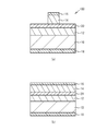
- FIG. 1A is a cross-sectional view in a direction parallel to the end face of the light emitting diode according to Example 1
- FIG. 1B is a cross-sectional view in a direction parallel to the side surface.
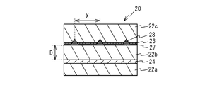
- FIG. 2 is a cross-sectional view illustrating an active layer portion of the light emitting diode according to the first embodiment.
- FIG. 3 is a top view showing quantum dots.
- 4A and 4B are cross-sectional views showing active layer portions of light emitting diodes according to Comparative Example 1 and Comparative Example 2.
- FIG. 5A and 5B are diagrams showing measurement results of electroluminescence measurement of the light emitting diodes of Comparative Example 1 and Comparative Example 2.
- FIG. 6 is a schematic diagram showing an emission spectrum of a light emitting diode having a hybrid structure.
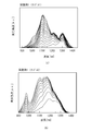
- 7A and 7B are diagrams showing measurement results of electroluminescence measurement of the light-emitting diode of Example 1.
- FIG. 8 is a cross-sectional view of the active layer portion for explaining the reason why the emission wavelength width is widened.
- FIG. 9 is a cross-sectional view illustrating the active layer portion of the light emitting diode according to the first modification of the first embodiment.
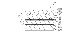
- FIG. 10 is a cross-sectional view illustrating an active layer portion of a light emitting diode according to Modification 2 of Example 1.
- FIG. 11 is a cross-sectional view illustrating an active layer portion of a light emitting diode according to Modification 3 of Example 1.
- FIG. 1A is a cross-sectional view in a direction parallel to the end face of the light-emitting diode according to Example 1
- FIG. 1B is a cross-sectional view in a direction parallel to the side surface.
- the light emitting diode 100 of Example 1 has a lower cladding layer 12 provided on a substrate 10.
- the substrate 10 is, for example, an n-type GaAs substrate.
- the lower cladding layer 12 is, for example, an n-type AlGaAs layer.
- a buffer layer that is, for example, an n-type GaAs layer may be provided between the substrate 10 and the lower cladding layer 12.
- An active layer portion 20 is provided on the lower cladding layer 12. Details of the active layer portion 20 will be described later.
- An upper cladding layer 14 is provided on the active layer portion 20.
- the upper cladding layer 14 has an isolated protrusion shape.
- the upper cladding layer 14 is, for example, a p-type AlGaAs layer.
- a p-electrode 16 is provided on the upper cladding layer 14, and an n-electrode 18 is provided under the substrate 10.
- the p electrode 16 is, for example, a metal film in which Au, Zn, and Au are stacked from the upper cladding layer 14 side.
- the n-electrode 18 is, for example, a metal film in which InGe and Au are stacked from the substrate 10 side.
- a contact layer for example, a p-type GaAs layer may be provided between the upper cladding layer 14 and the p-electrode 16.
- FIG. 2 is a cross-sectional view showing an active layer portion of the light emitting diode according to Example 1.
- the active layer portion 20 includes first to third barrier layers 22a to 22c, a quantum well layer 24, an InGaAs layer 26, a wetting layer 27, and a plurality of quantum dots 28.
- a quantum well layer 24 is provided on the first barrier layer 22 a, and a second barrier layer 22 b is provided on the quantum well layer 24.
- a plurality of quantum dots 28 are provided on the second barrier layer 22 b, and an InGaAs layer 26 is provided on the wetting layer 27 made of the same material as the plurality of quantum dots 28.
- a third barrier layer 22 c is provided on the plurality of quantum dots 28 and the InGaAs layer 26.
- the distance D between the quantum well layer 24 and the plurality of quantum dots 28 is the distance X between the centers of the plurality of quantum dots 28. It is smaller than the average value.
- the first barrier layer 22a to the third barrier layer 22c are made of a material having a larger band gap energy than the quantum well layer 24, and are, for example, GaAs layers.
- the quantum well layer 24 is, for example, an InGaAs layer.
- the plurality of quantum dots 28 are made of a material having a smaller band gap energy than the first barrier layer 22a to the third barrier layer 22c, and are made of, for example, InAs. Since the wetting layer 27 is made of the same material as the plurality of quantum dots 28, it is made of, for example, InAs.
- the plurality of quantum dots 28 are formed by a self-forming growth method based on a SK (Stranski-Krastanov) growth mode.
- a material having a lattice constant different from that of the substrate 10 for example, InAs
- two-dimensional layer growth occurs at first, and when the growth amount is increased, a lattice constant difference is caused.
- a plurality of quantum dots 28 are formed by transitioning to three-dimensional growth so as to suppress an increase in strain energy.
- FIG. 3 is a top view showing quantum dots. Note that the InGaAs layer 26 and the wetting layer 27 are not shown. As shown in FIG. 3, a plurality of quantum dots 28 are scattered on the second barrier layer 22b.
- the surface density of the plurality of quantum dots 28 is, for example, 1 ⁇ 10 9 to 1 ⁇ 10 11 cm ⁇ 2 .
- the surface density of the plurality of quantum dots 28 can be controlled by growth conditions, and is in the above range under general growth conditions. Under general growth conditions, the height of the quantum dots 28 is, for example, 4 to 12 nm, the diameter of the quantum dots 28 is, for example, 20-30 nm, and the average value of the intervals X between the centers of the plurality of quantum dots 28 is, for example, 25 nm. ⁇ 300 nm.
- the average value of the distance X between the centers of each of the plurality of quantum dots 28 can be obtained, for example, by calculating the square root of the reciprocal of the surface density of the plurality of quantum dots 28
- FIG. 4A and 4B are cross-sectional views showing active layer portions of light emitting diodes according to Comparative Example 1 and Comparative Example 2.
- FIG. 4A the active layer portion 80 of the light emitting diode of Comparative Example 1 has a structure in which a quantum well layer 84 is sandwiched between a first barrier layer 82a and a second barrier layer 82b. . Since the other structure of the light emitting diode of the comparative example 1 is the same as that of Example 1, description is abbreviate
- Comparative Example 1 is a light emitting diode having a quantum well structure.
- the active layer 90 of the light emitting diode of Comparative Example 2 includes a plurality of quantum dots 98 provided on the first barrier layer 92a, and a wetting layer 97 made of the same material as the plurality of quantum dots 98.
- An InGaAs layer 96 is provided thereon.
- the second barrier layer 92 b is provided on the plurality of quantum dots 98 and the InGaAs layer 96. Since the other structure of the light emitting diode of the comparative example 2 is the same as that of Example 1, description is abbreviate
- Comparative Example 2 is a light emitting diode having a quantum dot structure.
- the inventor produced the light emitting diodes of Comparative Example 1 and Comparative Example 2, and performed electroluminescence measurement.
- the specific configuration of the manufactured light emitting diode of Comparative Example 1 is shown in Table 1
- the specific configuration of the manufactured light emitting diode of Comparative Example 2 is shown in Table 2.
- the manufactured light emitting diode of Comparative Example 1 uses an n-type GaAs substrate as the substrate 10 and has a buffer layer composed of an n-type GaAs layer having a thickness of 200 nm between the substrate 10 and the lower cladding layer 12.
- a buffer layer composed of an n-type GaAs layer having a thickness of 200 nm between the substrate 10 and the lower cladding layer 12.
- As the lower cladding layer 12 an n-type Al 0.35 Ga 0.65 As layer having a thickness of 400 nm was used.
- the first barrier layer 82a constituting the active layer portion 80 is a 76.5 nm thick GaAs layer
- the quantum well layer 84 is a 7.0 nm thick In 0.34 Ga 0.66 As layer
- 82b is a GaAs layer having a thickness of 100 nm.
- a p-type Al 0.35 Ga 0.65 As layer having a thickness of 400 nm was used for the upper cladding layer 14.
- a contact layer made of a p-type GaAs layer having a thickness of 100 nm was provided on the upper clad layer 14.
- the first barrier layer 92a constituting the active layer portion 90 is a GaAs layer having a film thickness of 76.5 nm, and a plurality of quantum dots 98 are supplied in a supply amount of 0.7 nm.
- the thickness of InAs is about 5 nm
- the InGaAs layer 96 is an In 0.18 Ga 0.82 As layer having a thickness of 1.0 nm
- the second barrier layer 92b is a GaAs layer having a thickness of 100 nm.
- the surface density of the plurality of quantum dots 98 was 2 ⁇ 10 10 cm ⁇ 2 . Others were the same as the light emitting diode of Comparative Example 1 shown in Table 1.
- FIG. 5 (a) and 5 (b) are diagrams showing measurement results of electroluminescence measurement of the light emitting diodes of Comparative Example 1 and Comparative Example 2.
- FIG. The electroluminescence measurement was performed under an environmental temperature of 20 ° C., and for the light emitting diode of Comparative Example 1, the emission spectrum was measured by increasing the injection current from 0 mA to 400 mA in increments of 40 mA. For the light emitting diode, the emission spectrum was measured from 0 mA to 200 mA in increments of 20 mA.
- Comparative Example 1 which is a light emitting diode having a quantum well structure, has an emission peak wavelength in the vicinity of 1080 nm. As shown in FIG.
- Comparative Example 2 which is a light emitting diode having a quantum dot structure has emission peak wavelengths near 1190 nm and 1290 nm.
- Light emission having a peak near 1290 nm is light emission from the ground state, and light emission having a peak near 1190 nm is light emission from the first excited state.
- FIG. 6 is a schematic diagram showing an emission spectrum of a light emitting diode having a hybrid structure.
- light emission from the quantum well and light emission from the quantum dot are respectively generated, and a wide emission wavelength region can be obtained by superimposing light emission from each of the quantum well and the quantum dot.
- the light emission wavelength region cannot be expanded in a wavelength region where light emission from the quantum dot cannot be obtained.
- Example 1 an experiment performed on the light emitting diode according to Example 1 will be described.
- the inventor made two samples (sample 1 and sample 2) in which the film thicknesses of the first barrier layer 22a and the second barrier layer 22b constituting the active layer portion 20 were different, and performed electroluminescence measurement.
- Table 3 shows specific structures of the light-emitting diodes (Sample 1 and Sample 2) of Example 1 that were created.
- the first barrier layer 22a constituting the active layer portion 20 is a GaAs layer having a thickness of 56.5 nm
- the quantum well layer 24 is In 0.34 Ga 0 having a thickness of 7 nm. .66 As layer.
- the second barrier layer 22b is a GaAs layer having a thickness of 35.5 nm
- the plurality of quantum dots 28 is InAs having a supply amount of 0.7 nm
- the height is about 5 nm
- the InGaAs layer 26 is 1.0 nm in thickness.
- the third barrier layer 22c was a GaAs layer having a thickness of 100 nm.
- the surface density of the plurality of quantum dots 28 was 2 ⁇ 10 10 cm ⁇ 2 . That is, the average value between the centers of the plurality of quantum dots 28 was 70 nm. Others were the same as the light emitting diode of Comparative Example 1 shown in Table 1.
- the first barrier layer 22a constituting the active layer portion 20 is a GaAs layer having a thickness of 76.5 nm
- the quantum well layer 24 is an In 0.34 Ga 0.66 As layer having a thickness of 7 nm.
- the second barrier layer 22b is a GaAs layer having a thickness of 15.5 nm
- the plurality of quantum dots 28 is InAs for a supply amount of 0.7 nm
- the height is about 5 nm
- the InGaAs layer 26 is 1.0 nm in thickness.
- the third barrier layer 22c was a GaAs layer having a thickness of 100 nm.
- the surface density of the plurality of quantum dots 28 was 5 ⁇ 10 10 cm ⁇ 2 . That is, the average value between the centers of the plurality of quantum dots 28 was 45 nm. Others were the same as the light emitting diode of Comparative Example 1 shown in Table 1.
- FIGS. 7A and 7B are diagrams showing measurement results of electroluminescence measurement of the light emitting diode of Example 1.
- FIG. The electroluminescence measurement is performed at an ambient temperature of 20 ° C., and for sample 1, the emission current is measured by increasing the injection current from 0 mA to 300 mA in increments of 20 mA, and for sample 2, 0 mA is measured. The emission spectrum was measured at 10 mA increments up to 100 mA.
- FIGS. 7A and 7B the light-emitting diodes of Example 1 (Sample 1 and Sample 2) are shown in FIG. 5A with respect to light emission from a quantum well having an emission peak wavelength near 1080 nm.
- the emission wavelength width is wider than the light emitting diode of Comparative Example 1 shown in FIG.
- the light emission wavelength width (for example, 3 dB bandwidth) from the quantum well in the light emitting diode of Example 1 is about twice that of Comparative Example 1, for example.
- FIG. 7B there is a light emission peak near 980 nm, but it is unclear what causes the light emission.
- Example 1 the emission wavelength width from the quantum well is wider than that in Comparative Example 1, which is considered to be due to the following reason.
- FIG. 8 is a cross-sectional view of the active layer portion for explaining the reason why the emission wavelength width is widened. In FIG. 8, hatching is omitted for the sake of clarity.
- the quantum dots 28 formed by the self-forming growth method using the SK mode form a strain field (broken line) around the quantum dots 28. Since the distance D between the quantum well layer 24 and the plurality of quantum dots 28 is smaller than the average value of the distance X between the centers of the plurality of quantum dots 28, the influence of the strain field by the quantum dots 28 is influenced by the quantum well layer 24.
- the strain field caused by the quantum dots 28 reduces the band gap energy of the quantum well layer 24. Therefore, the band gap energy of the region 30 below the quantum dot 28 in the quantum well layer 24 is smaller than that of the region 32 below the central portion of the adjacent quantum dot 28. That is, the band gap energy of the quantum well layer 24 is modulated in a direction parallel to the upper surface of the substrate 10. Thereby, as shown in FIGS. 7A and 7B, it is considered that the emission wavelength width from the quantum well is widened.
- the active layer portion 20 includes a quantum well layer 24 and a plurality of quantum dots 28 arranged with the second barrier layer 22b sandwiched between the quantum well layer 24.
- the interval D between the quantum well layer 24 and the plurality of quantum dots 28 is smaller than the average value of the intervals X between the centers of the plurality of quantum dots 28. Therefore, as described with reference to FIG. 8, the band gap energy of the quantum well layer 24 is modulated in the direction parallel to the upper surface of the substrate 10 due to the influence of the strain field caused by the plurality of quantum dots 28.
- FIG. 7A and FIG. 7B the emission wavelength width from the quantum well can be widened, and as a result, a wide emission wavelength region can be realized.
- Non-Patent Document 1 it was difficult to widen the light emission wavelength region unless the light emission range was obtained from the quantum well and the quantum dot.
- the light emission from the quantum well was difficult. If it can be obtained, the emission wavelength range can be expanded. Therefore, for example, the emission wavelength region when a GaAs layer is used for the quantum well layer 24 can be widened, and a wide emission wavelength region can be realized in the range of 800 to 900 nm used for OCT of the eye.
- the case where the plurality of quantum dots 28 are made of a material that does not emit light may be used. In this case, the emission intensity from the quantum well due to the injection current can be increased. Of course, a wider emission wavelength range may be realized by emitting light from the plurality of quantum dots 28.
- the distance D between the quantum well layer 24 and the plurality of quantum dots 28 is too short, the size balance between a region where the influence of the strain field by the plurality of quantum dots 28 is large and a small region in the quantum well layer 24 is deteriorated. .
- the distance D between the quantum well layer 24 and the plurality of quantum dots 28 is too long, the influence of the strain field by the plurality of quantum dots 28 is uniformly received in the entire region of the quantum well layer 24.
- the distance D between the quantum well layer 24 and the plurality of quantum dots 28 is between the centers of the plurality of quantum dots 28.
- the thickness of the second barrier layer 22b between the quantum well layer 24 and the plurality of quantum dots 28 is a thickness at which a tunnel current does not flow between the quantum well layer 24 and the plurality of quantum dots 28. Is preferred. Thereby, the emitted light intensity from a quantum well can be raised.
- the quantum well layer 24 and the quantum dot 28 may be a III-V group compound semiconductor layer, and at least one of the quantum well layer 24 and the quantum dot 28 may include In as a group III element.
- the substrate 10 is a GaAs layer
- the quantum well layer 24 is an InGaAs layer
- the first to third barrier layers 22a to 22c are GaAs layers
- the plurality of quantum dots 28 are made of InAs.
- a structure in which light emission is performed in the range of 1000 nm to 1200 nm can be employed.
- the quantum well layer 24 may be formed of a GaAs layer. In this case, for example, AlInAs can be used as the plurality of quantum dots 28.
- the substrate 10 is a GaAs substrate
- the quantum well layer 24 is an AlGaInP layer
- the first to third barrier layers 22a to 22c are AlGaInP layers
- the plurality of quantum dots 28 are made of InP, and ranges from 630 nm to 850 nm from the quantum well. It is also possible to emit light.
- the substrate 10 is an InP substrate
- the quantum well layer 24 is an InGaAsP layer and an AlInGaAs layer
- the first to third barrier layers 22a to 22c are InGaAsP layers and an AlGaInGaAs layer
- a plurality of quantum dots 28 are made of InAs, and 1200 nm from the quantum well.
- the quantum well layer 24 and the quantum dot 28 may contain nitrogen (N) as a group V element.
- the substrate 10 is a GaN substrate
- the quantum well layer 24 is an InGaN layer
- ⁇ 22c may be an AlGaN layer
- the plurality of quantum dots 28 may be made of InN
- light emission of 300 nm to 600 nm may be performed from the quantum well.
- FIG. 9 is a cross-sectional view showing the active layer portion of the light emitting diode according to the first modification of the first embodiment.
- the positions of the quantum well layer 44 and the plurality of quantum dots 48 are opposite to those of the first embodiment. That is, a plurality of quantum dots 48 are provided on the first barrier layer 42 a, and an InGaAs layer 46 is provided on the wetting layer 47 made of the same material as the plurality of quantum dots 48.
- a second barrier layer 42 b is provided on the plurality of quantum dots 48 and the InGaAs layer 46.
- a quantum well layer 44 is provided on the second barrier layer 42 b, and a third barrier layer 42 c is provided on the quantum well layer 44. Since the other structure of the light emitting diode of the modification 1 of Example 1 is the same as that of Example 1, description is abbreviate
- the distance D between the quantum well layer 44 and the plurality of quantum dots 48 (that is, the distance between the lower surface of the quantum well layer 44 and the upper ends of the plurality of quantum dots 48) is set to a plurality of By making it smaller than the average value of the distance between the centers of the quantum dots 48, the emission wavelength width from the quantum well can be widened, and a wide emission wavelength range can be realized.
- FIG. 10 is a cross-sectional view showing an active layer portion of the light emitting diode according to the second modification of the first embodiment.
- the active layer portion 50 of the light emitting diode according to the second modification of the first embodiment includes the active layer portion 20 of the light emitting diode according to the first embodiment and the active layer portion 40 of the light emitting diode according to the first modification of the first embodiment. It has a structure that combines. That is, the first quantum well layer 54a is provided on the first barrier layer 52a, and the second barrier layer 52b is provided on the first quantum well layer 54a.
- a plurality of quantum dots 58 are provided on the second barrier layer 52 b, and an InGaAs layer 56 is provided on the wetting layer 57 made of the same material as the plurality of quantum dots 58.
- a third barrier layer 52 c is provided on the plurality of quantum dots 58 and the InGaAs layer 56.
- a second quantum well layer 54b is provided on the third barrier layer 52c, and a fourth barrier layer 52d is provided on the second quantum well layer 54b. Since the other structure of the light emitting diode of the modification 2 of Example 1 is the same as that of Example 1, description is abbreviate
- the distance D1 between the first quantum well layer 54a and the plurality of quantum dots 58 and the distance D2 between the second quantum well layer 54b and the plurality of quantum dots 58 are set to a plurality of quantum dots. 58 is made smaller than the average value of the distance between the centers. Thereby, the emission wavelength width from the quantum well can be widened, and a wide emission wavelength region can be realized.
- the active layer portion 50 includes a plurality of quantum well layers (first quantum well layer 54a and second quantum well layer 54b), the thicknesses of the first quantum well layer 54a and the second quantum well layer 54b are different from each other. The case is preferred. Thereby, a wider emission wavelength region can be realized.
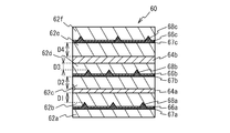
- FIG. 11 is a cross-sectional view showing an active layer portion of a light emitting diode according to Modification 3 of Example 1.
- the active layer portion 60 of the light emitting diode according to the third modification of the first embodiment includes a plurality of quantum dots on the upper side and the lower side of the active layer portion 50 of the light emitting diode according to the second modification of the first embodiment. It has a structure like that. That is, a plurality of first quantum dots 68a are provided on the first barrier layer 62a, and a first InGaAs layer 66a is provided on the first wetting layer 67a made of the same material as the plurality of first quantum dots 68a.
- a second barrier layer 62b is provided on the plurality of first quantum dots 68a and the first InGaAs layer 66a.
- a first quantum well layer 64a is provided on the second barrier layer 62b, and a third barrier layer 62c is provided on the first quantum well layer 64a.
- a plurality of second quantum dots 68b are provided on the third barrier layer 62c, and a second InGaAs layer 66b is provided on the second wetting layer 67b made of the same material as the plurality of second quantum dots 68b.
- a fourth barrier layer 62d is provided on the plurality of second quantum dots 68b and the second InGaAs layer 66b.
- a second quantum well layer 64b is provided on the fourth barrier layer 62d, and a fifth barrier layer 62e is provided on the second quantum well layer 64b.
- a plurality of third quantum dots 68c are provided on the fifth barrier layer 62e, and a third InGaAs layer 66c is provided on the third wetting layer 67c made of the same material as the plurality of third quantum dots 68c.
- a sixth barrier layer 62f is provided on the plurality of third quantum dots 68c and the third InGaAs layer 66c.
- the distance D1 between the first quantum well layer 64a and the plurality of first quantum dots 68a is smaller than the average value of the distance between the centers of the plurality of first quantum dots 68a.
- the distance D2 between the first quantum well layer 64a and the plurality of second quantum dots 68b and the distance D3 between the second quantum well layer 64b and the plurality of second quantum dots 68b are set between the centers of the plurality of second quantum dots 68b. It is made smaller than the average value of the interval.
- the interval D4 between the second quantum well layer 64b and the plurality of third quantum dots 68c is made smaller than the average value of the intervals between the centers of the plurality of third quantum dots 68c.
- the emission wavelength width from the quantum well can be widened, and a wide emission wavelength region can be realized.
- a wider emission wavelength region can be realized by making the thicknesses of the first quantum well layer 64a and the second quantum well layer 64b different from each other.
- the lower cladding layer is an n-type semiconductor and the upper cladding layer is a p-type semiconductor.
- the lower cladding layer is a p-type semiconductor and the upper cladding layer is an n-type semiconductor. It may be a semiconductor.
Landscapes
- Led Devices (AREA)
- Semiconductor Lasers (AREA)
Abstract
本発明は、基板10上に設けられた下部クラッド層12と、下部クラッド層12上に設けられ、量子井戸層24と、量子井戸層24との間に第2障壁層22bを挟んで配置された複数の量子ドット28と、を含む活性層部20と、活性層部20上に設けられた上部クラッド層14と、を備え、量子井戸層24と複数の量子ドット28との間隔Dは、複数の量子ドット28それぞれの中心間の間隔Xの平均値よりも小さい半導体発光素子である。
Description
本発明は、半導体発光素子に関する。
近年、例えばOCT(Optical Coherence Tomography)等の光センシングに向けて、発光波長域の広い発光素子が求められている。例えば、量子井戸-量子ドットのハイブリッド構造の半導体発光素子が提案されている(例えば、非特許文献1参照)。このハイブリッド構造の半導体発光素子は、量子井戸及び量子ドットからの互いに波長が異なる発光によって、広い発光波長域を実現している。また、自己形成された量子ドットの周辺に歪み場が形成され、この歪み場の影響が量子井戸層に及ぶと、量子井戸層のバンドギャップエネルギーが変化することが知られている(例えば、非特許文献2~4参照)。
Siming Chen、外7名、"Hybrid Quantum Well/Quantum Dot Structure for Broad Spectral Bandwidth Emitters"、IEEE JOURNAL OF SELECTED TOPICS IN QUANTUM ELECTRONICS、2013年、第19巻、第4号
John H. Davies、"Quantum dots induced by strain from buried and surface stressors"、APPLIED PHYSICS LETTERS、1999年、第75巻、第26号、p. 4141-4144
M. Sopanen、外2名、"Strain-induced quantum dots by self-organized stressors"、APPLIED PHYSICS LETTERS、1995年、第66巻、第18号、p. 2363-2366
H. Lipsanen、外2名、"Luminescence from excited states in strain-induced InxGa1-xAs quantum dots"、PHYSICAL REVIEW B、1995年、第51巻、第19号、p. 13868-13871
非特許文献1に記載の半導体発光素子では、量子井戸及び量子ドットそれぞれの発光を重ね合わせて、広い発光波長域を実現している。したがって、量子井戸及び量子ドットそれぞれからの発光が求められるため、例えば量子ドットからの発光が得られない波長域では発光波長域を広げられない等、改善の余地が残されている。
本発明は、上記課題に鑑みなされたものであり、広い発光波長域が実現可能な半導体発光素子を提供することを目的とする。
本発明は、基板上に設けられた下部クラッド層と、前記下部クラッド層上に設けられ、量子井戸層と、前記量子井戸層との間に障壁層を挟んで配置された複数の量子ドットと、を含む活性層部と、前記活性層部上に設けられた上部クラッド層と、を備え、前記量子井戸層と前記複数の量子ドットとの間隔は、前記複数の量子ドットそれぞれの中心間の間隔の平均値よりも小さいことを特徴とする半導体発光素子である。本発明によれば、広い発光波長域を実現することができる。
上記構成において、前記量子井戸層と前記複数の量子ドットとの間隔は、前記複数の量子ドットそれぞれの中心間の間隔の平均値の1/3以上且つ2/3以下である構成とすることができる。
上記構成において、前記量子井戸層と前記複数の量子ドットとの間の前記障壁層の厚さは、前記量子井戸層と前記複数の量子ドットとの間でトンネル電流が流れない厚さである構成とすることができる。
上記構成において、前記量子井戸層は、前記基板の上面に平行な方向において、前記複数の量子ドットによる歪み場の影響によって、バンドギャップエネルギーが変調されている構成とすることができる。
上記構成において、前記量子井戸層及び前記量子ドットはIII-V族化合物半導体層であり、前記量子井戸層及び前記量子ドットの少なくとも一方はIII族元素としてInを含む構成とすることができる。
上記構成において、前記量子井戸層はInGaAs層で、前記量子ドットはInAsである構成とすることができる。
上記構成において、前記量子井戸層はGaAs層で、前記量子ドットはAlInAsである構成とすることができる。
上記構成において、前記量子井戸層及び前記量子ドットの少なくとも一方はV族元素として窒素を含む構成とすることができる。
上記構成において、前記活性層部は複数の前記量子井戸層を含み、前記複数の量子井戸層の厚さは、互いに異なる構成とすることができる。
本発明によれば、広い発光波長域を実現することができる。
以下、図面を参照しつつ、本発明の実施例について説明する。
図1(a)は、実施例1に係る発光ダイオードの端面に平行な方向の断面図であり、図1(b)は、側面に平行な方向の断面図である。図1(a)及び図1(b)のように、実施例1の発光ダイオード100は、基板10上に下部クラッド層12が設けられている。基板10は、例えばn型GaAs基板である。下部クラッド層12は、例えばn型AlGaAs層である。なお、基板10と下部クラッド層12との間に、例えばn型GaAs層であるバッファ層が設けられていてもよい。
下部クラッド層12上に活性層部20が設けられている。活性層部20の詳細については後述する。活性層部20上に上部クラッド層14が設けられている。上部クラッド層14は孤立した突起形状をしている。上部クラッド層14は、例えばp型AlGaAs層である。上部クラッド層14上にp電極16が設けられ、基板10下にn電極18が設けられている。p電極16は、例えば上部クラッド層14側からAu、Zn、Auが積層された金属膜である。n電極18は、例えば基板10側からInGe、Auが積層された金属膜である。なお、上部クラッド層14とp電極16との間に、例えばp型GaAs層であるコンタクト層が設けられていてもよい。
図2は、実施例1に係る発光ダイオードの活性層部を示す断面図である。図2のように、活性層部20は、第1障壁層22a~第3障壁層22cと量子井戸層24とInGaAs層26と濡れ層27と複数の量子ドット28とを含む。第1障壁層22a上に量子井戸層24が設けられ、量子井戸層24上に第2障壁層22bが設けられている。第2障壁層22b上に複数の量子ドット28が設けられ、複数の量子ドット28と同じ材料の濡れ層27上にInGaAs層26が設けられている。これら複数の量子ドット28及びInGaAs層26上に、第3障壁層22cが設けられている。量子井戸層24と複数の量子ドット28との間隔D(即ち、量子井戸層24の上面と複数の量子ドット28の下端との間隔)は、複数の量子ドット28それぞれの中心間の間隔Xの平均値よりも小さくなっている。
第1障壁層22a~第3障壁層22cは、量子井戸層24よりもバンドギャップエネルギーの大きな材料からなり、例えばGaAs層である。量子井戸層24は、例えばInGaAs層である。複数の量子ドット28は、第1障壁層22a~第3障壁層22cよりもバンドギャップエネルギーの小さい材料からなり、例えばInAsからなる。濡れ層27は、複数の量子ドット28と同じ材料からなるため、例えばInAsからなる。複数の量子ドット28は、S-K(Stranski-Krastanov)成長モードを基礎とした自己形成成長法によって形成されている。つまり、基板10と異なる格子定数の材料(例えばInAs)を第2障壁層22b上にエピタキシャル成長させることで、初めは2次元的な層状成長が起こり、成長量を増やしていくと格子定数差を起因とする歪みエネルギーの増大を抑制するように3次元成長へと遷移して複数の量子ドット28が形成される。
図3は、量子ドットを示す上面図である。なお、InGaAs層26及び濡れ層27については図示を省略している。図3のように、第2障壁層22b上に、複数の量子ドット28が点在している。複数の量子ドット28の面密度は、例えば1×10⁹~1×1011cm-2である。複数の量子ドット28の面密度は、成長条件によって制御することができ、一般的な成長条件では、上記の範囲となる。また、一般的な成長条件では、量子ドット28の高さは例えば4~12nm、量子ドット28の直径は例えば20~30nm、複数の量子ドット28それぞれの中心間の間隔Xの平均値は例えば25nm~300nmとなる。複数の量子ドット28それぞれの中心間の間隔Xの平均値は、例えば複数の量子ドット28の面密度の逆数の平方根を計算することで求めることができる。
ここで、発明者が行った実験について説明する。まず、比較例1及び比較例2に係る発光ダイオードに対して行った実験について説明する。図4(a)及び図4(b)は、比較例1及び比較例2に係る発光ダイオードの活性層部を示す断面図である。図4(a)のように、比較例1の発光ダイオードの活性層部80は、第1障壁層82aと第2障壁層82bとの間に量子井戸層84が挟まれた構造をしている。比較例1の発光ダイオードのその他の構成は、実施例1と同じであるため説明を省略する。このように、比較例1は、量子井戸構造を有する発光ダイオードである。図4(b)のように、比較例2の発光ダイオードの活性層部90は、第1障壁層92a上に複数の量子ドット98が設けられ、複数の量子ドット98と同じ材料の濡れ層97上にInGaAs層96が設けられている。そして、これら複数の量子ドット98及びInGaAs層96上に、第2障壁層92bが設けられた構造をしている。比較例2の発光ダイオードのその他の構成は、実施例1と同じであるため説明を省略する。このように、比較例2は、量子ドット構造を有する発光ダイオードである。
発明者は、比較例1及び比較例2の発光ダイオードを作製し、エレクトロルミネッセンス測定を行った。作製した比較例1の発光ダイオードの具体的構成を表1に示し、作製した比較例2の発光ダイオードの具体的構成を表2に示す。

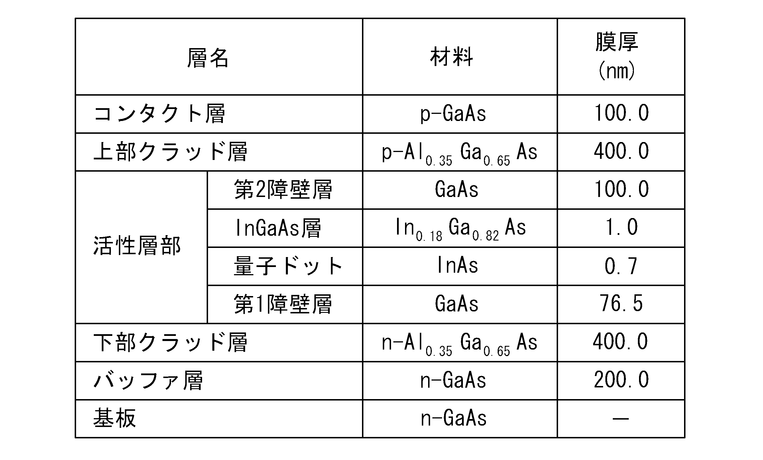
図5(a)及び図5(b)は、比較例1及び比較例2の発光ダイオードのエレクトロルミネッセンス測定の測定結果を示す図である。なお、エレクトロルミネッセンス測定は、20℃の環境温度の下で行い、比較例1の発光ダイオードに対しては、注入電流を0mAから40mA刻みで400mAまで上げて発光スペクトルを測定し、比較例2の発光ダイオードに対しては、0mAから20mA刻みで200mAまで上げて発光スペクトルを測定した。図5(a)のように、量子井戸構造を有する発光ダイオードである比較例1は、1080nm付近に発光ピーク波長を有している。図5(b)のように、量子ドット構造を有する発光ダイオードである比較例2は、1190nm付近と1290nm付近に発光ピーク波長を有している。1290nm付近にピークを有する発光は基底状態からの発光であり、1190nm付近にピークを有する発光は第1励起状態からの発光である。
ここで、非特許文献1のハイブリッド構造の発光ダイオードにおいて、量子井戸からの発光波長が量子ドットよりも短い場合での発光スペクトルについて説明する。図6は、ハイブリッド構造の発光ダイオードの発光スペクトルを示す模式図である。図6のように、量子井戸からの発光と量子ドットからの発光とがそれぞれ生じ、量子井戸及び量子ドットそれぞれからの発光を重ね合わせることで広い発光波長域を得ることができる。しかしながら、この場合では、量子井戸及び量子ドットそれぞれからの発光が求められるため、例えば量子ドットからの発光が得られない波長域では発光波長域を広げられない等の課題がある。
次に、実施例1に係る発光ダイオードに対して行った実験について説明する。発明者は、活性層部20を構成する第1障壁層22aと第2障壁層22bとの膜厚を異ならせた2つのサンプル(サンプル1及びサンプル2)を作製し、エレクトロルミネッセンス測定を行った。作成した実施例1の発光ダイオード(サンプル1及びサンプル2)の具体的構成を表3に示す。
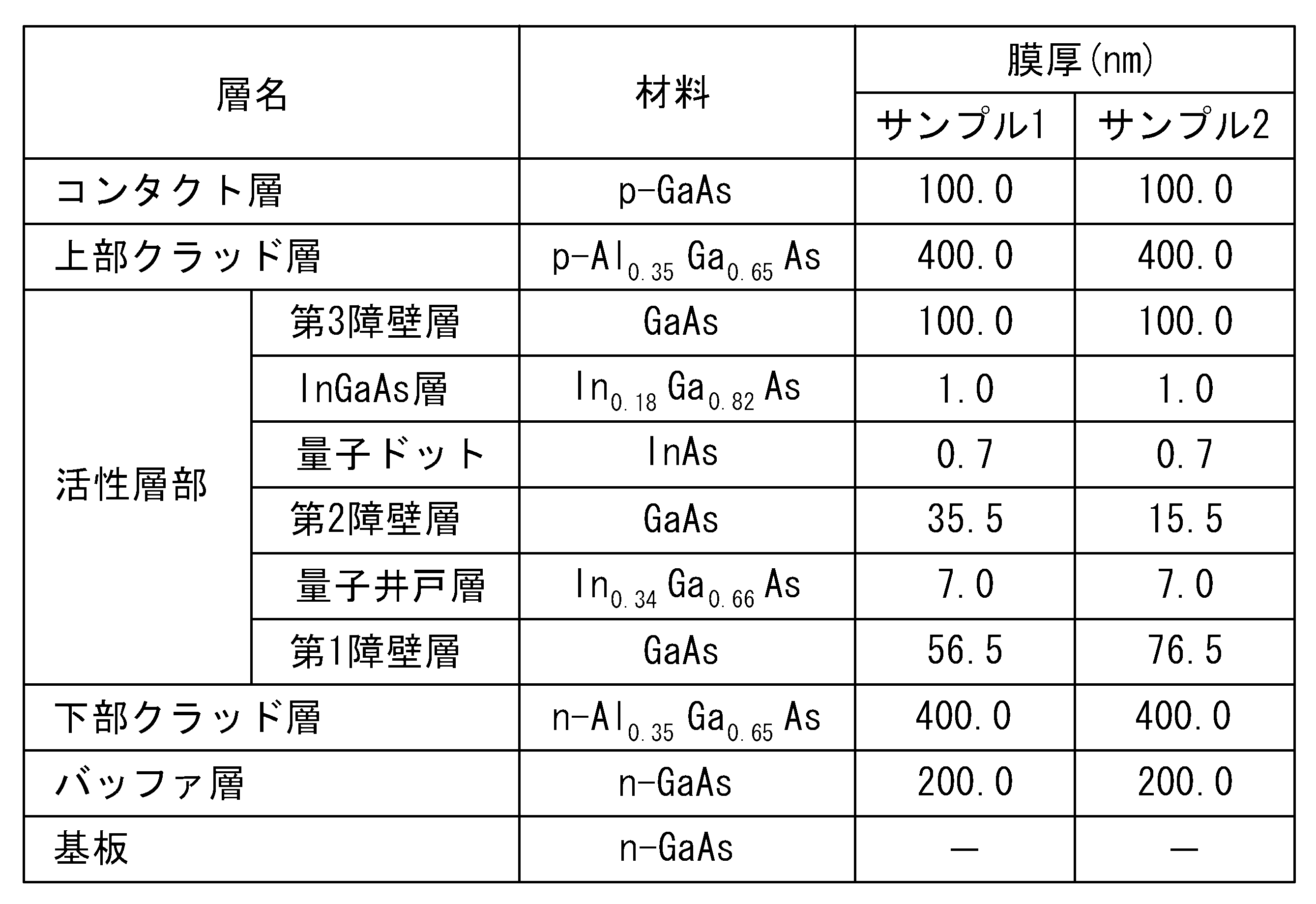
作製したサンプル2は、活性層部20を構成する第1障壁層22aを膜厚76.5nmのGaAs層とし、量子井戸層24を膜厚7nmのIn0.34Ga0.66As層とした。第2障壁層22bを膜厚15.5nmのGaAs層とし、複数の量子ドット28を供給量0.7nm厚分のInAsとして、その高さを5nm程度とし、InGaAs層26を膜厚1.0nmのIn0.18Ga0.82As層とし、第3障壁層22cを膜厚100nmのGaAs層とした。また、複数の量子ドット28の面密度は、5×1010cm-2であった。即ち、複数の量子ドット28それぞれの中心間の間隔の平均値は45nmであった。その他については、表1に示す比較例1の発光ダイオードと同じにした。
図7(a)及び図7(b)は、実施例1の発光ダイオードのエレクトロルミネッセンス測定の測定結果を示す図である。なお、エレクトロルミネッセンス測定は、20℃の環境温度の下で行い、サンプル1に対しては、注入電流を0mAから20mA刻みで300mAまで上げて発光スペクトルを測定し、サンプル2に対しては、0mAから10mA刻みで100mAまで上げて発光スペクトルを測定した。図7(a)及び図7(b)のように、1080nm付近に発光ピーク波長を有する量子井戸からの発光に関して、実施例1の発光ダイオード(サンプル1及びサンプル2)は、図5(a)に示す比較例1の発光ダイオードに比べて、発光波長幅が広がっていることが分かる。実施例1の発光ダイオードにおける量子井戸からの発光波長幅(例えば3dBバンド幅)は、比較例1に比べて、例えば2倍程度となっている。なお、図7(b)において、980nm付近にも発光のピークがあるが、これが何による発光なのかは不明である。
このように、実施例1では、比較例1に比べて、量子井戸からの発光波長幅が広がっているが、これは以下の理由によるものと考えられる。図8は、発光波長幅が広がった理由を説明するための活性層部の断面図である。なお、図8では、図の明瞭化のためにハッチを省略している。図8のように、S-Kモードによる自己形成成長法によって形成された量子ドット28は、その周辺に歪み場(破線)を形成する。量子井戸層24と複数の量子ドット28との間隔Dが、複数の量子ドット28それぞれの中心間の間隔Xの平均値よりも小さいため、量子ドット28による歪み場の影響は、量子井戸層24のうちの量子ドット28下の領域30では大きいが、近接する量子ドット28の中央部下の領域32では小さい。非特許文献2~4に記載されているように、量子ドット28による歪み場は、量子井戸層24のバンドギャップエネルギーを小さくする。したがって、量子井戸層24のうちの量子ドット28下の領域30のバンドギャップエネルギーは、近接する量子ドット28の中央部下の領域32よりも小さくなる。つまり、量子井戸層24のバンドギャップエネルギーは、基板10の上面に平行な方向において、変調されることとなる。これにより、図7(a)及び図7(b)のように、量子井戸からの発光波長幅が広がったものと考えられる。
実施例1によれば、活性層部20は、量子井戸層24と、量子井戸層24との間に第2障壁層22bを挟んで配置された複数の量子ドット28と、を含む。そして、量子井戸層24と複数の量子ドット28との間隔Dは、複数の量子ドット28それぞれの中心間の間隔Xの平均値よりも小さくなっている。このため、図8で説明したように、量子井戸層24は、基板10の上面に平行な方向において、複数の量子ドット28による歪み場の影響によって、バンドギャップエネルギーが変調される。これにより、図7(a)及び図7(b)のように、量子井戸からの発光波長幅を広げることができ、その結果、広い発光波長域を実現することができる。
非特許文献1に記載の発光ダイオードでは、量子井戸及び量子ドットそれぞれからの発光が得られる波長域でないと発光波長域を広げることが難しかったのに対し、実施例1では、量子井戸からの発光さえ得られれば、発光波長域を広げることが可能となる。したがって、例えば量子井戸層24にGaAs層を用いた場合での発光波長域を広げることもでき、眼のOCTに用いられる800~900nmにおいて広い発光波長域を実現することが可能となる。また、量子井戸からの発光さえ得られればよいことから、複数の量子ドット28から発光が生じない場合、例えば複数の量子ドット28が発光しない材料からなる場合でもよい。この場合、注入電流による量子井戸からの発光強度を強めることができる。勿論、複数の量子ドット28からも発光させることで、より広い発光波長域を実現するようにしてもよい。
量子井戸層24と複数の量子ドット28との間隔Dが短すぎると、量子井戸層24のうち複数の量子ドット28による歪み場の影響が大きい領域と小さい領域とのサイズバランスが悪くなってしまう。反対に、量子井戸層24と複数の量子ドット28の間隔Dが長すぎると、複数の量子ドット28による歪み場の影響を量子井戸層24の全領域で一様に受けるようになってしまう。このようなことを踏まえると、量子井戸層24のバンドギャップエネルギーを適切に変調させる観点から、量子井戸層24と複数の量子ドット28との間隔Dは、複数の量子ドット28それぞれの中心間の間隔Xの平均値の1/4以上且つ3/4以下である場合が好ましく、1/3以上且つ2/3以下である場合がより好ましく、2/5以上且つ3/5以下であることがさらに好ましく、1/2である場合がもっと好ましい。
また、量子井戸層24と複数の量子ドット28との間の第2障壁層22bの厚さは、量子井戸層24と複数の量子ドット28との間でトンネル電流が流れない厚さである場合が好ましい。これにより、量子井戸からの発光強度を高めることができる。
量子井戸層24及び量子ドット28はIII-V族化合物半導体層で、量子井戸層24及び量子ドット28の少なくとも一方はIII族元素としてInを含む構成とすることができる。例えば、実施例1のように、基板10がGaAs層、量子井戸層24がInGaAs層、第1~第3障壁層22a~22cがGaAs層、複数の量子ドット28がInAsからなり、量子井戸から1000nm~1200nmの範囲で発光がなされる構成とすることができる。また、上述したように、量子井戸層24がGaAs層からなる場合でもよく、この場合、複数の量子ドット28として例えばAlInAsを用いることができる。
また、例えば、基板10がGaAs基板、量子井戸層24がAlGaInP層、第1~第3障壁層22a~22cがAlGaInP層、複数の量子ドット28がInPからなり、量子井戸から630nm~850nmの範囲で発光がなされる場合でもよい。例えば、基板10がInP基板、量子井戸層24がInGaAsP層とAlInGaAs層、第1~第3障壁層22a~22cがInGaAsP層とAlGaInGaAs層、複数の量子ドット28がInAsからなり、量子井戸から1200nm~1700nmの発光がなされる場合でもよい。例えば、量子井戸層24及び量子ドット28の少なくとも一方がV族元素として窒素(N)を含む場合でもよく、基板10がGaN基板、量子井戸層24がInGaN層、第1~第3障壁層22a~22cがAlGaN層、複数の量子ドット28がInNからなり、量子井戸から300nm~600nmの発光がなされる場合でもよい。
図9は、実施例1の変形例1に係る発光ダイオードの活性層部を示す断面図である。図9のように、実施例1の変形例1の発光ダイオードの活性層部40は、実施例1と比較して、量子井戸層44と複数の量子ドット48の位置が反対となっている。つまり、第1障壁層42a上に複数の量子ドット48が設けられ、複数の量子ドット48と同じ材料の濡れ層47上にInGaAs層46が設けられている。これら複数の量子ドット48及びInGaAs層46上に、第2障壁層42bが設けられている。第2障壁層42b上に量子井戸層44が設けられ、量子井戸層44上に第3障壁層42cが設けられている。実施例1の変形例1の発光ダイオードのその他の構成は、実施例1と同じであるため説明を省略する。
実施例1の変形例1の場合でも、量子井戸層44と複数の量子ドット48との間隔D(即ち、量子井戸層44の下面と複数の量子ドット48の上端との間隔)を、複数の量子ドット48それぞれの中心間の間隔の平均値よりも小さくすることで、量子井戸からの発光波長幅を広げることができ、広い発光波長域を実現することができる。
図10は、実施例1の変形例2に係る発光ダイオードの活性層部を示す断面図である。図10のように、実施例1の変形例2の発光ダイオードの活性層部50は、実施例1の発光ダイオードの活性層部20と実施例1の変形例1の発光ダイオードの活性層部40とを組み合わせたような構造をしている。つまり、第1障壁層52a上に第1量子井戸層54aが設けられ、第1量子井戸層54a上に第2障壁層52bが設けられている。第2障壁層52b上に複数の量子ドット58が設けられ、複数の量子ドット58と同じ材料の濡れ層57上にInGaAs層56が設けられている。これら複数の量子ドット58及びInGaAs層56上に、第3障壁層52cが設けられている。第3障壁層52c上に第2量子井戸層54bが設けられ、第2量子井戸層54b上に第4障壁層52dが設けられている。実施例1の変形例2の発光ダイオードのその他の構成は、実施例1と同じであるため説明を省略する。
実施例1の変形例2の場合でも、第1量子井戸層54aと複数の量子ドット58との間隔D1及び第2量子井戸層54bと複数の量子ドット58との間隔D2を、複数の量子ドット58それぞれの中心間の間隔の平均値よりも小さくする。これにより、量子井戸からの発光波長幅を広げることができ、広い発光波長域を実現することができる。
また、活性層部50が複数の量子井戸層(第1量子井戸層54aと第2量子井戸層54b)を含む場合、第1量子井戸層54aと第2量子井戸層54bの厚さは互いに異なる場合が好ましい。これにより、より広い発光波長域を実現することができる。
図11は、実施例1の変形例3に係る発光ダイオードの活性層部を示す断面図である。図11のように、実施例1の変形例3の発光ダイオードの活性層部60は、実施例1の変形例2の発光ダイオードの活性層部50の上側及び下側に、さらに複数の量子ドットを設けたような構造をしている。つまり、第1障壁層62a上に複数の第1量子ドット68aが設けられ、複数の第1量子ドット68aと同じ材料の第1濡れ層67a上に第1InGaAs層66aが設けられている。これら複数の第1量子ドット68a及び第1InGaAs層66a上に、第2障壁層62bが設けられている。第2障壁層62b上に第1量子井戸層64aが設けられ、第1量子井戸層64a上に第3障壁層62cが設けられている。第3障壁層62c上に複数の第2量子ドット68bが設けられ、複数の第2量子ドット68bと同じ材料の第2濡れ層67b上に第2InGaAs層66bが設けられている。これら複数の第2量子ドット68b及び第2InGaAs層66b上に、第4障壁層62dが設けられている。第4障壁層62d上に第2量子井戸層64bが設けられ、第2量子井戸層64b上に第5障壁層62eが設けられている。第5障壁層62e上に複数の第3量子ドット68cが設けられ、複数の第3量子ドット68cと同じ材料の第3濡れ層67c上に第3InGaAs層66cが設けられている。これら複数の第3量子ドット68c及び第3InGaAs層66c上に、第6障壁層62fが設けられている。
実施例1の変形例3の場合でも、第1量子井戸層64aと複数の第1量子ドット68aとの間隔D1を、複数の第1量子ドット68aそれぞれの中心間の間隔の平均値よりも小さくする。第1量子井戸層64aと複数の第2量子ドット68bとの間隔D2及び第2量子井戸層64bと複数の第2量子ドット68bとの間隔D3を、複数の第2量子ドット68bそれぞれの中心間の間隔の平均値よりも小さくする。第2量子井戸層64bと複数の第3量子ドット68cとの間隔D4を、複数の第3量子ドット68cそれぞれの中心間の間隔の平均値よりも小さくする。これにより、量子井戸からの発光波長幅を広げることができ、広い発光波長域を実現することができる。また、第1量子井戸層64aと第2量子井戸層64bの厚さを互いに異ならせることで、より広い発光波長域を実現することができる。
実施例1では、下部クラッド層がn型半導体で、上部クラッド層がp型半導体の場合を例に示したが、反対の場合、即ち下部クラッド層がp型半導体で、上部クラッド層がn型半導体の場合でもよい。
以上、発明の好ましい実施例について詳述したが、本発明は係る特定の実施例に限定されるものではなく、特許請求の範囲に記載された本発明の要旨の範囲内において、種々の変形・変更が可能である。
Claims (9)
- 基板上に設けられた下部クラッド層と、
前記下部クラッド層上に設けられ、量子井戸層と、前記量子井戸層との間に障壁層を挟んで配置された複数の量子ドットと、を含む活性層部と、
前記活性層部上に設けられた上部クラッド層と、を備え、
前記量子井戸層と前記複数の量子ドットとの間隔は、前記複数の量子ドットそれぞれの中心間の間隔の平均値よりも小さいことを特徴とする半導体発光素子。 - 前記量子井戸層と前記複数の量子ドットとの間隔は、前記複数の量子ドットそれぞれの中心間の間隔の平均値の1/3以上且つ2/3以下であることを特徴とする請求項1記載の半導体発光素子。
- 前記量子井戸層と前記複数の量子ドットとの間の前記障壁層の厚さは、前記量子井戸層と前記複数の量子ドットとの間でトンネル電流が流れない厚さであることを特徴とする請求項1または2記載の半導体発光素子。
- 前記量子井戸層は、前記基板の上面に平行な方向において、前記複数の量子ドットによる歪み場の影響によって、バンドギャップエネルギーが変調されていることを特徴とする請求項1から3のいずれか一項記載の半導体発光素子。
- 前記量子井戸層及び前記量子ドットはIII-V族化合物半導体層であり、前記量子井戸層及び前記量子ドットの少なくとも一方はIII族元素としてInを含むことを特徴とする請求項1から4のいずれか一項記載の半導体発光素子。
- 前記量子井戸層はInGaAs層で、前記量子ドットはInAsであることを特徴とする請求項5記載の半導体発光素子。
- 前記量子井戸層はGaAs層で、前記量子ドットはAlInAsであることを特徴とする請求項5記載の半導体発光素子。
- 前記量子井戸層及び前記量子ドットの少なくとも一方はV族元素として窒素を含むことを特徴とする請求項5記載の半導体発光素子。
- 前記活性層部は複数の前記量子井戸層を含み、
前記複数の量子井戸層の厚さは、互いに異なることを特徴とする請求項1から8のいずれか一項記載の半導体発光素子。
Priority Applications (3)
| Application Number | Priority Date | Filing Date | Title |
|---|---|---|---|
| EP15740889.9A EP3101697B1 (en) | 2014-01-27 | 2015-01-07 | Semiconductor light-emitting element |
| CN201580005722.9A CN105934832B (zh) | 2014-01-27 | 2015-01-07 | 半导体发光元件 |
| US15/110,991 US9865771B2 (en) | 2014-01-27 | 2015-01-07 | Semiconductor light-emitting element |
Applications Claiming Priority (2)
| Application Number | Priority Date | Filing Date | Title |
|---|---|---|---|
| JP2014-012838 | 2014-01-27 | ||
| JP2014012838A JP6174499B2 (ja) | 2014-01-27 | 2014-01-27 | 半導体発光素子 |
Publications (1)
| Publication Number | Publication Date |
|---|---|
| WO2015111432A1 true WO2015111432A1 (ja) | 2015-07-30 |
Family
ID=53681240
Family Applications (1)
| Application Number | Title | Priority Date | Filing Date |
|---|---|---|---|
| PCT/JP2015/050266 Ceased WO2015111432A1 (ja) | 2014-01-27 | 2015-01-07 | 半導体発光素子 |
Country Status (5)
| Country | Link |
|---|---|
| US (1) | US9865771B2 (ja) |
| EP (1) | EP3101697B1 (ja) |
| JP (1) | JP6174499B2 (ja) |
| CN (1) | CN105934832B (ja) |
| WO (1) | WO2015111432A1 (ja) |
Families Citing this family (5)
| Publication number | Priority date | Publication date | Assignee | Title |
|---|---|---|---|---|
| CN107394017B (zh) * | 2017-07-31 | 2019-02-05 | 天津三安光电有限公司 | 发光二极管及其制备方法 |
| JP7543862B2 (ja) * | 2020-11-13 | 2024-09-03 | 株式会社デンソー | 半導体レーザ装置 |
| CN113193089B (zh) * | 2021-04-30 | 2022-06-24 | 湖南汇思光电科技有限公司 | 基于掺杂(Si)GeSn有源区的CMOS技术兼容硅基光源器件及其制备方法 |
| US12334714B2 (en) * | 2021-05-21 | 2025-06-17 | The Board Of Trustees Of The University Of Illinois | Visible light-emitting device and laser with improved tolerance to crystalline defects and damage |
| CN113471341A (zh) * | 2021-05-26 | 2021-10-01 | 厦门大学 | 一种基于红光AlInGaAs量子点的Micro-LED结构及其制备方法 |
Citations (4)
| Publication number | Priority date | Publication date | Assignee | Title |
|---|---|---|---|---|
| JP2005072338A (ja) * | 2003-08-26 | 2005-03-17 | Fujitsu Ltd | 光半導体装置及びその製造方法 |
| JP2008078578A (ja) * | 2006-09-25 | 2008-04-03 | Toshiba Corp | 半導体装置および化合物半導体基板とその製造方法 |
| JP2009065143A (ja) * | 2008-08-08 | 2009-03-26 | Technical Research & Development Institute Ministry Of Defence | 光半導体装置 |
| JP2012109434A (ja) * | 2010-11-18 | 2012-06-07 | Technical Research & Development Institute Ministry Of Defence | 量子ドット型赤外線検知器及び赤外線イメージセンサ |
Family Cites Families (17)
| Publication number | Priority date | Publication date | Assignee | Title |
|---|---|---|---|---|
| JP3672678B2 (ja) * | 1996-04-05 | 2005-07-20 | 富士通株式会社 | 量子半導体装置およびその製造方法 |
| US6816525B2 (en) * | 2000-09-22 | 2004-11-09 | Andreas Stintz | Quantum dot lasers |
| JP2004537854A (ja) * | 2001-07-31 | 2004-12-16 | ザ ボード オブ トラスティース オブ ザ ユニバーシティ オブ イリノイ | 結合した量子ドット及び量子井戸の半導体デバイス及びデバイス形成方法 |
| TWI235504B (en) * | 2003-03-19 | 2005-07-01 | Chung Shan Inst Of Science | The structure and fabrication method of infrared quantum dot light emitting diode |
| KR100631980B1 (ko) * | 2005-04-06 | 2006-10-11 | 삼성전기주식회사 | 질화물 반도체 소자 |
| CN101038946A (zh) * | 2006-03-16 | 2007-09-19 | 中国科学院半导体研究所 | 半导体量子点/量子阱导带内跃迁材料结构 |
| CN101589478B (zh) * | 2006-09-08 | 2013-01-23 | 新加坡科技研究局 | 可调波长发光二极管 |
| JP4861112B2 (ja) * | 2006-09-27 | 2012-01-25 | 富士通株式会社 | 光半導体装置及びその製造方法 |
| JP2008235442A (ja) * | 2007-03-19 | 2008-10-02 | Fujitsu Ltd | 半導体発光素子及びその製造方法 |
| KR101404143B1 (ko) * | 2007-10-12 | 2014-06-05 | 에이전시 포 사이언스, 테크놀로지 앤드 리서치 | 인이 함유되지 않은 레드 및 화이트 질소 기반 led 제조 |
| JP5704987B2 (ja) * | 2011-03-25 | 2015-04-22 | 富士フイルム株式会社 | 波長変換素子および光電変換装置 |
| EP2523218A2 (en) * | 2011-05-09 | 2012-11-14 | Sharp Kabushiki Kaisha | Solar Cell |
| GB2492771A (en) * | 2011-07-11 | 2013-01-16 | Univ Sheffield | broadband optical device structure and method of fabrication thereof |
| CN202534677U (zh) * | 2012-04-13 | 2012-11-14 | 苏辉 | 基于量子点和量子阱材料混合结构的超辐射发光管 |
| JP2013239690A (ja) * | 2012-04-16 | 2013-11-28 | Sharp Corp | 超格子構造、前記超格子構造を備えた半導体装置および半導体発光装置、ならびに前記超格子構造の製造方法 |
| KR20160018869A (ko) * | 2013-07-03 | 2016-02-17 | 인피닉스, 인크. | Ss-oct 시스템에 대한 파장-튜닝가능 수직 캐비티 표면 방출 레이저 |
| KR20160069393A (ko) * | 2014-12-08 | 2016-06-16 | 엘지전자 주식회사 | 광 변환 복합재의 제조방법, 광 변환 복합재, 이를 포함하는 광 변환 필름, 백라이트 유닛 및 표시장치 |
-
2014
- 2014-01-27 JP JP2014012838A patent/JP6174499B2/ja not_active Expired - Fee Related
-
2015
- 2015-01-07 EP EP15740889.9A patent/EP3101697B1/en active Active
- 2015-01-07 CN CN201580005722.9A patent/CN105934832B/zh not_active Expired - Fee Related
- 2015-01-07 US US15/110,991 patent/US9865771B2/en not_active Expired - Fee Related
- 2015-01-07 WO PCT/JP2015/050266 patent/WO2015111432A1/ja not_active Ceased
Patent Citations (4)
| Publication number | Priority date | Publication date | Assignee | Title |
|---|---|---|---|---|
| JP2005072338A (ja) * | 2003-08-26 | 2005-03-17 | Fujitsu Ltd | 光半導体装置及びその製造方法 |
| JP2008078578A (ja) * | 2006-09-25 | 2008-04-03 | Toshiba Corp | 半導体装置および化合物半導体基板とその製造方法 |
| JP2009065143A (ja) * | 2008-08-08 | 2009-03-26 | Technical Research & Development Institute Ministry Of Defence | 光半導体装置 |
| JP2012109434A (ja) * | 2010-11-18 | 2012-06-07 | Technical Research & Development Institute Ministry Of Defence | 量子ドット型赤外線検知器及び赤外線イメージセンサ |
Non-Patent Citations (5)
| Title |
|---|
| H. LIPSANEN: "Luminescence from excited states in strain-induced InxGal-xAs quantum dots", PHYSICAL REVIEW B, vol. 51, no. 19, 1995, pages 13868 - 13871 |
| JOHN H. DAVIES: "Quantum dots induced by strain from buried and surface stressors", APPLIED PHYSICS LETTERS, vol. 75, no. 26, 1999, pages 4141 - 4144, XP012024354, DOI: doi:10.1063/1.125563 |
| M. SOPANEN: "Strain-induced quantum dots by self-organized stressors", APPLIED PHYSICS LETTERS, vol. 66, no. 18, 1995, pages 2363 - 2366, XP002183027, DOI: doi:10.1063/1.113984 |
| See also references of EP3101697A4 |
| SIMING CHEN: "Hybrid Quantum Well/Quantum Dot Structure for Broad Spectral Bandwidth Emitters", IEEE JOURNAL OF SELECTED TOPICS IN QUANTUM ELECTRONICS, vol. 19, no. 4, 2013, XP011508626, DOI: doi:10.1109/JSTQE.2012.2235175 |
Also Published As
| Publication number | Publication date |
|---|---|
| CN105934832B (zh) | 2018-12-28 |
| JP6174499B2 (ja) | 2017-08-02 |
| US9865771B2 (en) | 2018-01-09 |
| EP3101697B1 (en) | 2022-03-23 |
| EP3101697A1 (en) | 2016-12-07 |
| JP2015141951A (ja) | 2015-08-03 |
| EP3101697A4 (en) | 2017-08-16 |
| US20160336480A1 (en) | 2016-11-17 |
| CN105934832A (zh) | 2016-09-07 |
Similar Documents
| Publication | Publication Date | Title |
|---|---|---|
| JP5238865B2 (ja) | 半導体発光素子 | |
| US9048378B2 (en) | Device with inverted large scale light extraction structures | |
| CN103733449B (zh) | 氮化物半导体紫外线发光元件 | |
| TWI529960B (zh) | 具有差排彎折結構之發光裝置 | |
| CN112072467B (zh) | 半导体雷射二极管 | |
| US20190207055A1 (en) | Method of manufacturing semiconductor optical device and semiconductor optical device | |
| JP6174499B2 (ja) | 半導体発光素子 | |
| JP2016129266A5 (ja) | ||
| JP2009530803A5 (ja) | モノリシック白色発光ダイオード及びその製造方法 | |
| JP2009170921A (ja) | AlInGaN発光デバイス | |
| US20130292644A1 (en) | Semiconductor light emitting device | |
| JP3754226B2 (ja) | 半導体発光素子 | |
| JP5908967B2 (ja) | 窒化物系発光装置 | |
| US20120201264A1 (en) | Light emitting device with varying barriers | |
| CN104821353B (zh) | 发光二极管‑半导体元件 | |
| US20170062660A1 (en) | Nitride semiconductor stacked body and semiconductor light emitting device | |
| WO2018020793A1 (ja) | 半導体発光素子および半導体発光素子の製造方法 | |
| CN106898948A (zh) | 超辐射发光二极管或激光器外延结构及其制备方法 | |
| US20230079101A1 (en) | Micrometer scale light-emitting diodes | |
| TWI818268B (zh) | 具有載子再利用機制的垂直共振腔表面放射雷射二極體 | |
| CN103579427A (zh) | 半导体发光器件及其制造方法 | |
| KR101937592B1 (ko) | 양자우물구조를 이용한 자외선 광소자 | |
| JP2007035936A (ja) | 半導体発光素子 | |
| CN102136534A (zh) | 砷化镓基短波长量子点超辐射发光二极管 | |
| US20210320224A1 (en) | Light-emitting device |
Legal Events
| Date | Code | Title | Description |
|---|---|---|---|
| 121 | Ep: the epo has been informed by wipo that ep was designated in this application |
Ref document number: 15740889 Country of ref document: EP Kind code of ref document: A1 |
|
| REEP | Request for entry into the european phase |
Ref document number: 2015740889 Country of ref document: EP |
|
| WWE | Wipo information: entry into national phase |
Ref document number: 2015740889 Country of ref document: EP |
|
| WWE | Wipo information: entry into national phase |
Ref document number: 15110991 Country of ref document: US |
|
| NENP | Non-entry into the national phase |
Ref country code: DE |