WO2015111490A1 - Élément de circuit non réciproque - Google Patents
Élément de circuit non réciproque Download PDFInfo
- Publication number
- WO2015111490A1 WO2015111490A1 PCT/JP2015/050887 JP2015050887W WO2015111490A1 WO 2015111490 A1 WO2015111490 A1 WO 2015111490A1 JP 2015050887 W JP2015050887 W JP 2015050887W WO 2015111490 A1 WO2015111490 A1 WO 2015111490A1
- Authority
- WO
- WIPO (PCT)
- Prior art keywords
- input
- center electrode
- output port
- series
- resistance element
- Prior art date
- Legal status (The legal status is an assumption and is not a legal conclusion. Google has not performed a legal analysis and makes no representation as to the accuracy of the status listed.)
- Ceased
Links
Images


Classifications
-
- H—ELECTRICITY
- H01—ELECTRIC ELEMENTS
- H01P—WAVEGUIDES; RESONATORS, LINES, OR OTHER DEVICES OF THE WAVEGUIDE TYPE
- H01P1/00—Auxiliary devices
- H01P1/32—Non-reciprocal transmission devices
- H01P1/36—Isolators
-
- H—ELECTRICITY
- H01—ELECTRIC ELEMENTS
- H01P—WAVEGUIDES; RESONATORS, LINES, OR OTHER DEVICES OF THE WAVEGUIDE TYPE
- H01P1/00—Auxiliary devices
- H01P1/32—Non-reciprocal transmission devices
- H01P1/38—Circulators
- H01P1/383—Junction circulators, e.g. Y-circulators
-
- H—ELECTRICITY
- H01—ELECTRIC ELEMENTS
- H01P—WAVEGUIDES; RESONATORS, LINES, OR OTHER DEVICES OF THE WAVEGUIDE TYPE
- H01P1/00—Auxiliary devices
- H01P1/32—Non-reciprocal transmission devices
- H01P1/38—Circulators
- H01P1/383—Junction circulators, e.g. Y-circulators
- H01P1/387—Strip line circulators
-
- H—ELECTRICITY
- H03—ELECTRONIC CIRCUITRY
- H03H—IMPEDANCE NETWORKS, e.g. RESONANT CIRCUITS; RESONATORS
- H03H7/00—Multiple-port networks comprising only passive electrical elements as network components
- H03H7/01—Frequency selective two-port networks
- H03H7/0115—Frequency selective two-port networks comprising only inductors and capacitors
-
- H—ELECTRICITY
- H03—ELECTRONIC CIRCUITRY
- H03H—IMPEDANCE NETWORKS, e.g. RESONANT CIRCUITS; RESONATORS
- H03H7/00—Multiple-port networks comprising only passive electrical elements as network components
- H03H7/18—Networks for phase shifting
-
- H—ELECTRICITY
- H03—ELECTRONIC CIRCUITRY
- H03H—IMPEDANCE NETWORKS, e.g. RESONANT CIRCUITS; RESONATORS
- H03H7/00—Multiple-port networks comprising only passive electrical elements as network components
- H03H7/52—One-way transmission networks, i.e. unilines
-
- H—ELECTRICITY
- H05—ELECTRIC TECHNIQUES NOT OTHERWISE PROVIDED FOR
- H05K—PRINTED CIRCUITS; CASINGS OR CONSTRUCTIONAL DETAILS OF ELECTRIC APPARATUS; MANUFACTURE OF ASSEMBLAGES OF ELECTRICAL COMPONENTS
- H05K1/00—Printed circuits
- H05K1/18—Printed circuits structurally associated with non-printed electric components
- H05K1/182—Printed circuits structurally associated with non-printed electric components associated with components mounted in printed circuit boards [PCB], e.g. insert-mounted components [IMC]
Definitions
- the present invention relates to non-reciprocal circuit elements, and more particularly to non-reciprocal circuit elements such as isolators and circulators used in the microwave band.
- nonreciprocal circuit elements such as isolators and circulators have a characteristic of transmitting a signal only in a predetermined specific direction and not transmitting in a reverse direction. Utilizing this characteristic, for example, an isolator is used in a transmission circuit unit of a mobile communication device such as a mobile phone.
- Patent Document 1 discloses that two center electrodes 21 and 22 (inductance elements L1 and L2) formed on a ferrite 10 and capacitors C1 and C2 are 2 as shown in FIG. A pair of LC parallel resonance circuits is configured, and a resistor element R is connected in series between one end of each of the center electrodes 21 and 22 is described.
- Patent Document 2 it is described that the isolation characteristic is broadened by connecting an LC series resonance circuit to a resistance element.
- the technique described in Patent Document 2 attempts to widen the isolation characteristic by matching the resistance element to a wide band according to the resonance characteristic of the LC series resonance circuit.
- JP 2001-237613 A Japanese Patent No. 4155342
- An object of the present invention is to provide a non-reciprocal circuit device capable of obtaining good isolation characteristics over a wide band.
- the nonreciprocal circuit device is A magnetic material to which a DC magnetic field is applied by a permanent magnet; A plurality of central electrodes arranged to intersect with each other in a magnetically insulated state; With Of the plurality of center electrodes, one end of the first center electrode is connected to the first input / output port, and one end of the second center electrode is connected to the second input / output port.
- a resistance element is connected in series between the first input / output port and the second input / output port, and a phase shift circuit is connected in series to the resistance element; It is characterized by.
- the non-reciprocal circuit device is A magnetic material to which a DC magnetic field is applied by a permanent magnet; A first center electrode, a second center electrode, and a third center electrode, which are arranged in an insulating state and intersecting the magnetic body; With The first center electrode has one end connected to the first input / output port and the other end connected to the ground.
- the third center electrode has one end connected to the third input / output port, the other end connected to the ground, Capacitance elements are respectively connected in parallel to the first center electrode, the second center electrode, and the third center electrode to form a first LC parallel resonance circuit, a second LC parallel resonance circuit, and a third LC parallel resonance circuit, A resistance element is connected in series between the first input / output port and the second input / output port, and a phase shift circuit is connected in series to the resistance element; It is characterized by.
- the non-reciprocal circuit device is A magnetic material to which a DC magnetic field is applied by a permanent magnet; A first center electrode and a second center electrode, which are arranged in an insulating state and intersecting the magnetic body; With The first center electrode has one end connected to the first input / output port and the other end connected to the ground.
- Capacitance elements are respectively connected in parallel to the first center electrode and the second center electrode to form a first LC parallel resonance circuit and a second LC parallel resonance circuit, A resistance element is connected in series between the first input / output port and the second input / output port, and a phase shift circuit is connected in series to the resistance element; It is characterized by.
- the nonreciprocal circuit element when a high frequency signal is input in the opposite direction, a phase difference in potential occurs between the first input / output port and the second input / output port, and a current flows through the resistance element to increase the high frequency signal. Attenuated. Since the phase shift circuit is connected in series with the resistance element, this phase difference becomes large over a wide band, and the isolation characteristic is improved over the wide band.
- FIG. 3 is an exploded perspective view showing the ferrite / magnet assembly shown in FIG. 2. It is a graph which shows the phase characteristic of the said nonreciprocal circuit element. It is a graph which shows the isolation characteristic of the said nonreciprocal circuit element. It is a graph which shows the insertion loss characteristic of the said nonreciprocal circuit element. It is the equivalent circuit schematic of the nonreciprocal circuit device which is 2nd Example. It is the equivalent circuit schematic of the nonreciprocal circuit device which is 3rd Example. It is the equivalent circuit schematic of the nonreciprocal circuit device which is 4th Example. It is the equivalent circuit schematic of the nonreciprocal circuit device which is 5th Example. It is an equivalent circuit diagram of the conventional nonreciprocal circuit device. It is a graph which shows the phase characteristic of the nonreciprocal circuit device shown in FIG.
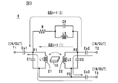
- the nonreciprocal circuit device is constituted by an equivalent circuit shown in FIG. That is, a pair of permanent magnets 31 (see FIGS. 2 and 3), a magnetic body 10 to which a DC magnetic field is applied by the permanent magnets 31 (hereinafter referred to as ferrite), and the ferrite 10 are arranged so as to cross each other in an insulated state.
- the first center electrode 21 and the second center electrode 22 are provided.
- the first center electrode 21 has one end connected to the first input / output port P1 and the other end connected to the ground.
- the second center electrode 22 has one end connected to the second input / output port P2 and the other end connected to the ground.
- Capacitance elements C1 and C2 are connected in parallel to the first center electrode 21 and the second center electrode 22, respectively, to form a first LC parallel resonance circuit and a second LC parallel resonance circuit.
- a resistance element R is connected in series between the first input / output port P1 and the second input / output port P2, and a phase shift circuit (an LC parallel resonance circuit including an inductance element L5 and a capacitance element C5) is provided.
- the resistor element R is connected in series.
- an input impedance matching capacitive element Cs1 is connected between the first input / output port P1 and the input terminal IN.
- a capacitive element Cs2 for output impedance matching is connected between the second input / output port P2 and the output terminal OUT.
- the two-port isolator 1 having the above circuit configuration, when a high-frequency signal is input from the input terminal IN to the port P1 (forward direction), the ports P1 and P2 are in phase and no current flows through the resistance element R. Therefore, it is transmitted to the output terminal OUT with a small insertion loss. Since a high frequency signal does not flow through the LC parallel resonance circuit composed of the inductance element L5 and the capacitive element C5, the insertion loss does not increase.
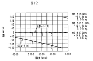
- FIG. 4 shows the phase difference characteristics in the reverse direction in the first embodiment.
- FIG. 12 shows the phase difference characteristics in the reverse direction in the conventional example shown in FIG.
- the first embodiment shown in FIG. 4 produces a larger phase difference than the conventional example shown in FIG.
- the phase differences at each frequency are shown in Tables 1A and 1B below.
- the phase differences at each frequency in the forward direction are shown in Tables 1C and 1D below.
- the isolation characteristic of the conventional example shown in FIG. 11 is as shown by a curve B in FIG.
- the frequency band having an isolation characteristic of 15 dB or less is wider than that of the conventional example, and the isolation characteristic is improved over a wide band.
- the attenuation amount of the isolation characteristic at each frequency is shown in Table 1E below.
- the specific insertion loss characteristic is as shown by the curve A in FIG.
- the insertion loss characteristic of the conventional example shown in FIG. 11 is as shown by a curve B in FIG.
- the insertion loss near 5150 MHz is improved in the first embodiment. This is because the resonant frequency of the LC parallel resonant circuit composed of the inductance element L5 and the capacitive element C5 is set near 5150 MHz, so that the impedance on the transmission route (2) side to which the resistance element R is connected is infinite at that frequency. This is because the high frequency signal hardly flows to the resistance element R.
- the isolation characteristic is broadened by connecting an LC series resonance circuit to the resistance element.
- the broadband of the isolation characteristic is achieved by matching the resistance element in a wide band by the impedance characteristic of the LC series resonance circuit.
- the LC parallel resonant circuit composed of the elements L5 and C5 is connected in series to the resistance element R, so that the transmission routes (1) and (2) The phase difference of the high frequency signal is increased to improve the isolation characteristics.
- the lumped constant type two-port isolator 1 includes a ferrite / magnet assembly 9 in which permanent magnets 31 are bonded to the front and back surfaces of the ferrite 10 via adhesives 32, respectively.
- the assembly 9 is mounted on the multilayer substrate 6 so that the main surface of the ferrite 10 is in the vertical direction.
- a yoke 8 is disposed immediately above the assembly 9.
- the first center electrode 21 is wound around the front and back surfaces of the ferrite 10 for one turn, the one end electrode 21a is the port P1, and the other end electrode 21b is the ground port.
- the second center electrode 22 is wound four turns on the front and back surfaces of the ferrite 10 so as to intersect with the first center electrode 21 at a predetermined angle while maintaining an insulating state. The number of windings is arbitrary.
- One end electrode 22a of the second center electrode 22 is a port P2, and the other end is common (ground port) with the electrode 21b.
- FIG. 3 the illustration of the electrode on the back side of the ferrite 10 is omitted to avoid complication.
- the circuit elements (capacitance elements C1, C2, C5, Cs1, Cs2, inductance element L5) are built in the multilayer substrate 6. By incorporating at least one of these circuit elements in the multilayer substrate 6, the isolator 1 can be reduced in size.
- phase difference between the high-frequency signal (reverse direction) that is input from the output terminal OUT and flows through the transmission route (1) and the high-frequency signal that flows through the transmission route (2) is closer to 180 degrees, the better effect is obtained. For this reason, even if it is not the LC parallel resonance circuit, the phase difference between the high-frequency signal (reverse direction) flowing through the transmission route (1) and the high-frequency signal flowing through the transmission route (2) is brought close to 180 degrees in a predetermined frequency band. It is only necessary to provide a phase shift circuit having a function. As an example of such a phase shift circuit, for example, a stripline type transmission line can be used.
- the nonreciprocal circuit element (two-port isolator 2) according to the second embodiment has a reactance element X connected in parallel to the resistance element R, as shown in FIG.
- the configuration is the same as that of the isolator 1 according to one embodiment.
- the operational effect of the second embodiment is basically the same as that of the first embodiment.
- This type of capacitive element or inductance element may be mounted on a multilayer substrate as a chip type, or may be formed and incorporated as an internal electrode on the multilayer substrate.
- the capacitance value and the inductance value can be adjusted by cutting the internal electrode pattern with a laser or a leuter.
- the nonreciprocal circuit device (2-port isolator 3) according to the third embodiment is one in which a capacitive element Cj is further connected in series between the first port P1 and the output terminal OUT.
- Other configurations are the same as those of the isolator 1 according to the first embodiment.
- the operational effects of the third embodiment are basically the same as those of the first embodiment.
- the capacitive element Cj is for impedance matching between the ports P1 and P2, and by changing the capacitance value of the capacitive element Cj, the attenuation of the isolation characteristic and the insertion loss characteristic can be finely adjusted. Therefore, by providing the capacitive element Cj, desired characteristics can be easily obtained.
- the nonreciprocal circuit device (four-port circulator 4) of the fourth embodiment has the other end of the first center electrode 21 and the other end of the second center electrode 22 connected to the third input / output port P3.
- the port P3 is connected to the input / output terminal T3 via the impedance matching capacitive element Cs3.
- an input / output unit at one end (input / output port P1) of the first center electrode 21 is a terminal T1
- an input / output unit at one end (input / output port P2) of the second center electrode 22 is a terminal T2.
- Other configurations are basically the same as those of the isolator 1 according to the first embodiment.
- the high frequency signal input to the terminal T1 is transmitted to the terminal T2.
- the high-frequency signal input to the terminal T2 is mainly transmitted to the terminal T3 based on the resonance frequencies of the elements L2 and C2, and the signal component transmitted from the terminal T2 to the terminal T1 is attenuated by the resistance element R. Further, as described in the first embodiment, the phase difference between the LC parallel resonant circuit transmission route 1 and the transmission route 2 is adjusted to 180 degrees by the elements L5 and C5, and the isolation characteristics are improved.
- the high-frequency signal input to the terminal T3 is transmitted to the terminal T1 based on the resonance frequency of the elements L1 and C1, and is not transmitted to the terminal T2.
- the nonreciprocal circuit device (three-port circulator 5) according to the fifth embodiment has a third center electrode 23 as a ferrite 10 in addition to the first center electrode 21 and the second center electrode 22.
- the center electrodes 21 and 22 are arranged so as to intersect with each other in an insulated state.
- One end of the third center electrode 23 corresponds to the third input / output port P3, and the port P3 is connected to the terminal T3 via the impedance matching capacitive element Cs3.
- the other end of the third center electrode 23 is connected to the ground.
- the capacitive element C3 is connected in parallel to the third center electrode 23 to form a third parallel resonant circuit.
- an input / output unit at one end (input / output port P1) of the first center electrode 21 is a terminal T1
- an input / output unit at one end (input / output port P2) of the second center electrode 22 is a terminal T2.
- Other configurations are basically the same as those of the isolator 1 according to the first embodiment.
- the high-frequency signal input to the terminal T1 is transmitted to the terminal T2.
- the high-frequency signal input to the terminal T2 is transmitted to the terminal T3 based on the resonance frequencies of the elements L2 and C2 and the resonance frequencies of the elements L3 and C3, and the signal component leaking to the terminal T1 is attenuated by the resistance element R.
- the phase difference between the LC parallel resonant circuit transmission route 1 and the transmission route 2 is adjusted to 180 degrees by the elements L5 and C5, and the isolation characteristic between the terminal T1 and the terminal T2 is adjusted. Will be good.
- the high-frequency signal input to the terminal T3 is transmitted to the terminal T1 based on the resonance frequencies of the elements L1 and C1 and the resonance frequencies of the elements L3 and C3, and transmitted to the terminal T2 due to the irreversibility of the ferrite. Absent.
- a circuit including a resistor R and elements L5 and C5 installed between the input / output ports P1 and P2 is provided between the input / output ports P2 and P3 or between the input / output ports P3 and P1. Also good.
- the element value of element L5, C5 can be adjusted appropriately between each port, and the isolation characteristic between each port can be made favorable.
- the non-reciprocal circuit device according to the present invention is not limited to the above-described embodiments, and can be variously modified within the scope of the gist thereof.
- the configuration of the ferrite / magnet assembly 9, in particular, the shapes of the first and second center electrodes 21, 22 are arbitrary.
- the present invention is useful for non-reciprocal circuit devices, and is particularly excellent in that good isolation characteristics can be obtained over a wide band.
Landscapes
- Engineering & Computer Science (AREA)
- Microelectronics & Electronic Packaging (AREA)
- Power Engineering (AREA)
- Non-Reversible Transmitting Devices (AREA)
Abstract
L'invention a pour objet d'obtenir une caractéristique d'isolation favorable sur une large bande dans un élément de circuit non réciproque et réalise à cet effet un élément de circuit non réciproque comprenant un corps magnétique (10) auquel un champ magnétique à courant continu est appliqué par un aimant permanent, et une pluralité d'électrodes centrales qui sont disposées sur le corps magnétique (10) de manière à se croiser mutuellement en étant isolées. Parmi la pluralité d'électrodes centrales, une première électrode centrale (21) possède une extrémité raccordée à un premier port d'entrée/sortie (P1) et une deuxième électrode centrale (22) possède une extrémité raccordée à un deuxième port d'entrée/sortie (P2). Un élément résistif (R) est branché en série entre les ports (P1, P2) et un circuit de déphasage (un circuit résonant parallèle constitué d'un élément inductif (L5) et d'un élément capacitif (C5)) est branché en série avec l'élément résistif (R).
Priority Applications (3)
| Application Number | Priority Date | Filing Date | Title |
|---|---|---|---|
| CN201580005724.8A CN105934850B (zh) | 2014-01-27 | 2015-01-15 | 不可逆电路元件 |
| JP2015558814A JP6152896B2 (ja) | 2014-01-27 | 2015-01-15 | 非可逆回路素子 |
| US15/219,680 US9728831B2 (en) | 2014-01-27 | 2016-07-26 | Non-reciprocal circuit element |
Applications Claiming Priority (2)
| Application Number | Priority Date | Filing Date | Title |
|---|---|---|---|
| JP2014-012254 | 2014-01-27 | ||
| JP2014012254 | 2014-01-27 |
Related Child Applications (1)
| Application Number | Title | Priority Date | Filing Date |
|---|---|---|---|
| US15/219,680 Continuation US9728831B2 (en) | 2014-01-27 | 2016-07-26 | Non-reciprocal circuit element |
Publications (1)
| Publication Number | Publication Date |
|---|---|
| WO2015111490A1 true WO2015111490A1 (fr) | 2015-07-30 |
Family
ID=53681296
Family Applications (1)
| Application Number | Title | Priority Date | Filing Date |
|---|---|---|---|
| PCT/JP2015/050887 Ceased WO2015111490A1 (fr) | 2014-01-27 | 2015-01-15 | Élément de circuit non réciproque |
Country Status (4)
| Country | Link |
|---|---|
| US (1) | US9728831B2 (fr) |
| JP (1) | JP6152896B2 (fr) |
| CN (1) | CN105934850B (fr) |
| WO (1) | WO2015111490A1 (fr) |
Citations (3)
| Publication number | Priority date | Publication date | Assignee | Title |
|---|---|---|---|---|
| JP2009302742A (ja) * | 2008-06-11 | 2009-12-24 | Murata Mfg Co Ltd | 非可逆回路素子 |
| JP2011176668A (ja) * | 2010-02-25 | 2011-09-08 | Murata Mfg Co Ltd | 非可逆回路素子 |
| JP2012028856A (ja) * | 2010-07-20 | 2012-02-09 | Murata Mfg Co Ltd | 非可逆回路素子 |
Family Cites Families (6)
| Publication number | Priority date | Publication date | Assignee | Title |
|---|---|---|---|---|
| JP3264194B2 (ja) * | 1995-12-13 | 2002-03-11 | 株式会社村田製作所 | 非可逆回路素子 |
| CA2214617C (fr) * | 1996-09-06 | 2000-12-19 | Toshihiro Makino | Circuit non reversible |
| JP3412593B2 (ja) * | 2000-02-25 | 2003-06-03 | 株式会社村田製作所 | 非可逆回路素子および高周波回路装置 |
| JP4155342B1 (ja) | 2007-08-31 | 2008-09-24 | 株式会社村田製作所 | 非可逆回路素子 |
| US7532084B2 (en) * | 2007-08-31 | 2009-05-12 | Murata Manufacturing Co., Ltd | Nonreciprocal circuit element |
| JP5508173B2 (ja) | 2009-07-29 | 2014-05-28 | 株式会社ダイセル | 積層セラミック部品製造用溶剤組成物 |
-
2015
- 2015-01-15 WO PCT/JP2015/050887 patent/WO2015111490A1/fr not_active Ceased
- 2015-01-15 CN CN201580005724.8A patent/CN105934850B/zh not_active Expired - Fee Related
- 2015-01-15 JP JP2015558814A patent/JP6152896B2/ja not_active Expired - Fee Related
-
2016
- 2016-07-26 US US15/219,680 patent/US9728831B2/en not_active Expired - Fee Related
Patent Citations (3)
| Publication number | Priority date | Publication date | Assignee | Title |
|---|---|---|---|---|
| JP2009302742A (ja) * | 2008-06-11 | 2009-12-24 | Murata Mfg Co Ltd | 非可逆回路素子 |
| JP2011176668A (ja) * | 2010-02-25 | 2011-09-08 | Murata Mfg Co Ltd | 非可逆回路素子 |
| JP2012028856A (ja) * | 2010-07-20 | 2012-02-09 | Murata Mfg Co Ltd | 非可逆回路素子 |
Also Published As
| Publication number | Publication date |
|---|---|
| CN105934850A (zh) | 2016-09-07 |
| JP6152896B2 (ja) | 2017-06-28 |
| US9728831B2 (en) | 2017-08-08 |
| JPWO2015111490A1 (ja) | 2017-03-23 |
| US20160336634A1 (en) | 2016-11-17 |
| CN105934850B (zh) | 2018-11-16 |
Similar Documents
| Publication | Publication Date | Title |
|---|---|---|
| CN103081219B (zh) | 非可逆电路元件 | |
| US8253510B2 (en) | Non-reciprocal circuit element | |
| JP5679056B2 (ja) | 非可逆回路素子 | |
| JP5843007B2 (ja) | 非可逆回路素子 | |
| JP5983859B2 (ja) | 非可逆回路素子及びモジュール | |
| JPWO2009028112A1 (ja) | 非可逆回路素子 | |
| JPWO2008087782A1 (ja) | 非可逆回路素子 | |
| WO2015029680A1 (fr) | Isolateur | |
| JP6152896B2 (ja) | 非可逆回路素子 | |
| CN104584320B (zh) | 不可逆电路元件 | |
| JP5655990B2 (ja) | 非可逆回路素子 | |
| JP5573178B2 (ja) | 非可逆回路素子 | |
| JPWO2016158044A1 (ja) | 非可逆回路素子、高周波回路及び通信装置 | |
| JPWO2013118355A1 (ja) | 非可逆回路素子 | |
| WO2015093273A1 (fr) | Élément circuit non réciproque | |
| JP5652116B2 (ja) | 非可逆回路素子 | |
| JP2012138719A (ja) | 非可逆回路素子及びフェライト・磁石素子 | |
| WO2014115596A1 (fr) | Élément de circuit du type à deux ports à transmission non réciproque | |
| WO2014115595A1 (fr) | Élément de circuit irréversible | |
| JP2012095068A (ja) | 非可逆回路素子 | |
| WO2007013252A1 (fr) | Élément de circuit irréversible, composants électroniques composites et dispositif de communication | |
| JP2012090141A (ja) | 非可逆回路素子 | |
| JP2012231202A (ja) | 非可逆回路素子及びフェライト・磁石素子 |
Legal Events
| Date | Code | Title | Description |
|---|---|---|---|
| 121 | Ep: the epo has been informed by wipo that ep was designated in this application |
Ref document number: 15740466 Country of ref document: EP Kind code of ref document: A1 |
|
| ENP | Entry into the national phase |
Ref document number: 2015558814 Country of ref document: JP Kind code of ref document: A |
|
| NENP | Non-entry into the national phase |
Ref country code: DE |
|
| 122 | Ep: pct application non-entry in european phase |
Ref document number: 15740466 Country of ref document: EP Kind code of ref document: A1 |