WO2015111576A1 - スパッタリングターゲット - Google Patents
スパッタリングターゲット Download PDFInfo
- Publication number
- WO2015111576A1 WO2015111576A1 PCT/JP2015/051395 JP2015051395W WO2015111576A1 WO 2015111576 A1 WO2015111576 A1 WO 2015111576A1 JP 2015051395 W JP2015051395 W JP 2015051395W WO 2015111576 A1 WO2015111576 A1 WO 2015111576A1
- Authority
- WO
- WIPO (PCT)
- Prior art keywords
- sputtering
- region
- target material
- target
- sputtering target
- Prior art date
- Legal status (The legal status is an assumption and is not a legal conclusion. Google has not performed a legal analysis and makes no representation as to the accuracy of the status listed.)
- Ceased
Links
Images







Classifications
-
- C—CHEMISTRY; METALLURGY
- C23—COATING METALLIC MATERIAL; COATING MATERIAL WITH METALLIC MATERIAL; CHEMICAL SURFACE TREATMENT; DIFFUSION TREATMENT OF METALLIC MATERIAL; COATING BY VACUUM EVAPORATION, BY SPUTTERING, BY ION IMPLANTATION OR BY CHEMICAL VAPOUR DEPOSITION, IN GENERAL; INHIBITING CORROSION OF METALLIC MATERIAL OR INCRUSTATION IN GENERAL
- C23C—COATING METALLIC MATERIAL; COATING MATERIAL WITH METALLIC MATERIAL; SURFACE TREATMENT OF METALLIC MATERIAL BY DIFFUSION INTO THE SURFACE, BY CHEMICAL CONVERSION OR SUBSTITUTION; COATING BY VACUUM EVAPORATION, BY SPUTTERING, BY ION IMPLANTATION OR BY CHEMICAL VAPOUR DEPOSITION, IN GENERAL
- C23C14/00—Coating by vacuum evaporation, by sputtering or by ion implantation of the coating forming material
- C23C14/22—Coating by vacuum evaporation, by sputtering or by ion implantation of the coating forming material characterised by the process of coating
- C23C14/34—Sputtering
- C23C14/3407—Cathode assembly for sputtering apparatus, e.g. Target
-
- H—ELECTRICITY
- H01—ELECTRIC ELEMENTS
- H01J—ELECTRIC DISCHARGE TUBES OR DISCHARGE LAMPS
- H01J37/00—Discharge tubes with provision for introducing objects or material to be exposed to the discharge, e.g. for the purpose of examination or processing thereof
- H01J37/32—Gas-filled discharge tubes
- H01J37/34—Gas-filled discharge tubes operating with cathodic sputtering
- H01J37/3411—Constructional aspects of the reactor
- H01J37/3414—Targets
- H01J37/3423—Shape
-
- H—ELECTRICITY
- H01—ELECTRIC ELEMENTS
- H01J—ELECTRIC DISCHARGE TUBES OR DISCHARGE LAMPS
- H01J37/00—Discharge tubes with provision for introducing objects or material to be exposed to the discharge, e.g. for the purpose of examination or processing thereof
- H01J37/32—Gas-filled discharge tubes
- H01J37/34—Gas-filled discharge tubes operating with cathodic sputtering
- H01J37/3411—Constructional aspects of the reactor
- H01J37/3414—Targets
-
- H—ELECTRICITY
- H01—ELECTRIC ELEMENTS
- H01J—ELECTRIC DISCHARGE TUBES OR DISCHARGE LAMPS
- H01J37/00—Discharge tubes with provision for introducing objects or material to be exposed to the discharge, e.g. for the purpose of examination or processing thereof
- H01J37/32—Gas-filled discharge tubes
- H01J37/34—Gas-filled discharge tubes operating with cathodic sputtering
- H01J37/3411—Constructional aspects of the reactor
- H01J37/3414—Targets
- H01J37/3426—Material
-
- H—ELECTRICITY
- H01—ELECTRIC ELEMENTS
- H01J—ELECTRIC DISCHARGE TUBES OR DISCHARGE LAMPS
- H01J2237/00—Discharge tubes exposing object to beam, e.g. for analysis treatment, etching, imaging
- H01J2237/32—Processing objects by plasma generation
- H01J2237/33—Processing objects by plasma generation characterised by the type of processing
- H01J2237/332—Coating
Definitions
- the present invention relates to a sputtering target.
- an inert gas such as argon is introduced under vacuum and a high DC voltage is applied between the substrate and the target material to cause the plasma (or ionized) inert gas to collide with the target material.
- target atoms contained in the target material are knocked out, the hit atoms are deposited on the substrate, and a thin film is formed on the substrate.
- magnetron sputtering in which a magnet is disposed on the back side of a sputtering surface of a target material (that is, a surface on which a plasma (or ionized) inert gas collides with the target material) to increase the deposition rate. ing.
- a sputtering target used for such sputtering generally includes a target material having a flat disk-shaped surface, and the sputtering surface is circular.
- Patent Document 1 discloses a sputtering target having a long lifetime.
- the distance between the sputtering surface of the target material and the substrate (hereinafter sometimes referred to as “TS distance”) is reduced, so in the initial stage of sputtering.
- the film thickness uniformity of the thin film formed on the substrate is lowered.
- the target material erosion becomes severe with time (particularly near the outer periphery of the target material) and the target material is difficult to consume (particularly the target material).
- the sputtering is performed for a long time, the difference becomes large, and the film thickness uniformity of the thin film formed on the substrate is greatly reduced.
- the film thickness uniformity of the thin film formed on the substrate can be improved at any stage from the initial stage of sputtering to the end thereof. It was difficult to secure.
- the present inventor has found that a circular flat first region located in the center of the sputtering surface of the target material of the sputtering target and a first region concentrically with the first region outside the first region.
- a ring-shaped second region disposed in the first region, and the first region is disposed at a position that is at most 15% lower than the thickness of the second region with respect to the second region,
- a long life of 1800 kWh or more can be achieved with integrated power, and an excellent thin film formed on the substrate in the meantime.
- the present inventors have found that thickness uniformity can be ensured and have completed the present invention.
- the present invention provides the following sputtering target, but the disclosure in the present specification is not limited to the following sputtering target.
- a sputtering target including a target material, wherein the target material has a circular flat first region located in the center on the sputtering surface, and a concentric shape with the first region outside the first region.
- the first region is disposed at a position that is at most 15% lower than the thickness of the second region with respect to the second region.
- the sputtering target is characterized in that the diameter of the first region is 60% to 80% of the diameter of the outer periphery of the sputtering surface.
- the present invention it is possible to achieve both a long life of the sputtering target, particularly a long life of 1800 kWh or more and excellent film thickness uniformity in a thin film formed on the substrate therebetween.
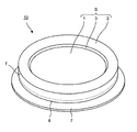
- the perspective view which shows one Embodiment of the sputtering target of this invention.
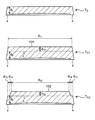
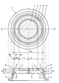
- the top view and sectional drawing which show typically one Embodiment of the sputtering target of this invention.
- Cross-sectional view of the target material T schematically shows the sputtering target of the target material T 0 and the invention of the sputtering target of standard shape.
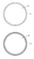
- Sectional view respectively showing schematically a sputtering target of the target material T 0 and Comparative Examples 1 and 2 sputtering target target material Tc 1 and Tc 2 standard shape.
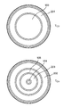
- Target material T 0 and Comparative Examples 3 and sectional views respectively schematically showing the sputtering target of the target material Tc 3 and Tc 4 of 4 of the sputtering target of standard shape.
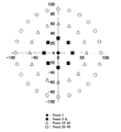
- FIG. 5 is a schematic diagram showing measurement points (Points 1 to 49) of sheet resistance values ( ⁇ / ⁇ ) at 49 points of a thin film on a substrate having a diameter of 200 mm.
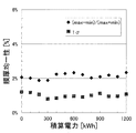
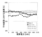
- the graph which shows the film thickness uniformity at the time of using the sputtering target of a reference example (standard shape).
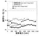
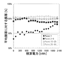
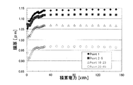
- the graph which shows the relationship between integrated electric power and the film thickness of the thin film formed on a board
- sputtering target of the present invention will be described in detail below with reference to specific embodiments with reference to the accompanying drawings. However, the sputtering target of the present invention is not limited to the following embodiment.
- FIGS. 1 and 2 One embodiment of the sputtering target of the present invention is schematically shown in FIGS. 1 and 2 is schematically shown for illustration, and actual dimensions and shapes are as defined in this specification.
- the sputtering target 10 of the present invention includes a target material T as shown in FIGS.
- the target material T includes a sputtering surface S that receives an inert gas that has been plasmatized (or ionized) by sputtering.
- the sputtering surface S has a circular flat first region 1 located at the center thereof, and a ring-shaped first region that is located outside the first region 1 and is concentrically arranged with the first region 1. 2 region 2.
- both the first region 1 and the second region 2 are shown as planes, but these are not limited to planes.
- the first region 1 can be disposed parallel to each other preferably at a position (vertically below) that is at most 15% lower than the second region 2 with respect to the thickness of the second region.
- the target material T has a sputtering surface S composed of the first region 1, the second region 2, and the intermediate region 3 thereof.
- the sputtering surface S has a circular outer periphery (the outer periphery of the sputtering surface S coincides with the outer periphery of the second region 2), and the first region
- the diameter of 1 is 60% to 80%, preferably 60% to 75%, more preferably 65% to 75%, and still more preferably 67% to 72% of the diameter of the outer periphery of the sputtering surface S.
- the sputtering target 10 of the present invention has the above-described configuration, it can achieve a long life of 1800 kWh or more when sputtering using a sputtering apparatus such as a magnetron sputtering apparatus, and is equivalent to or equivalent to a conventional product.
- a thin film having the above film thickness uniformity can be formed on the substrate over 0 to 1800 kWh or more.
- aluminum is preferable.
- an aluminum alloy is also preferable as the material of the target material T, and the aluminum alloy may contain a metal such as copper or silicon, and the content thereof is, for example, 2% by weight or less, preferably 1% by weight. It is as follows.
- the target material T includes a circular and flat first region 1, a second region 2, and an intermediate region 3 as necessary. Can be formed.
- the diameter d 4 of the sputtering surface S is, for example, in the range of 260 mm to 325 mm.
- the back surface 4 of the target material T (that is, the surface opposite to the sputtering surface S) preferably has a circular outer periphery, and the outer periphery has a diameter in the range of 330 mm to 345 mm, for example.
- the back surface 4 of the target material T may be formed in a conical shape with the center of the circle as a vertex.
- the depth of the dent is usually 1 mm to 3 mm at the apex.
- the peripheral portion (or side surface) 5 of the target material T is a surface that is linearly continuous from the end of the second region 2 to the joint portion x with the support member 6.
- the peripheral edge 5 has a tapered surface or a cylinder whose radial size increases as it proceeds from the end of the second region 2 toward the joint x with the support member 6.
- the surface may be a shape.
- the peripheral portion “having no step” means that the peripheral portion of the target material has a continuous surface, and an arbitrary step is not intentionally formed.
- the joint portion x of the target material T is a ring-shaped convex portion (vertically below) as shown in the figure, but the height is not particularly limited. Further, the joint portion x of the target material T may form a plane together with the back surface 4 of the target material T (that is, may be flush).
- the peripheral portion 5 of the target material T has no step, and by providing the peripheral portion 5 having no step as the side surface of the target material, the film thickness uniformity of the sputtering target is improved, and as a result, the target The life of the material is improved.
- peripheral part 5 you may have several taper surfaces from which an angle differs continuously without a level
- First region 1 As shown in FIG. 2, the first region 1 is located in the center of the sputtering surface S, has a circular flat shape, and is disposed at a position lower than the second region 2 (vertically below). It is what is done.
- the fact that the first region 1 is “flat” means that no convex portion or concave portion is substantially formed in the first region 1.
- the protrusions and recesses are not substantially formed” in the first region 1 means that no protrusions or recesses are intentionally formed in the first region 1.
- the first region 1 is shown as a plane. However, as long as it is flat as described above, the first region 1 is not limited to such a plane.
- the first region 1 is circular, and its radius r 1 is, for example, 95 mm to 130 mm, preferably 95 mm to 125 mm, more preferably 105 mm to 125 mm, and still more preferably 108 mm to 117 mm.
- the distance d 1 (vertical direction) between the first region 1 and the second region 2 is at most 15%, preferably 4% to 12% with respect to the thickness d 3 of the second region 2 More preferably, it is 4% to 8%.
- the distance d 1 between the first region 1 and the second region 2 is shown in actual dimensions, it is, for example, 4 mm or less, more preferably 1 mm to 3 mm, and more preferably 1 mm to 2 mm.
- the film thickness uniformity of the thin film formed on the substrate can be improved.
- the thickness d 2 of the target material T in the first region 1 a conventional standard (the sputtering surface diameter: 8 inches life: 1200KWh) and a thickness of 19.6mm or more, for example 20 mm ⁇ 30 mm, preferably It is 23 mm to 28 mm.
- the back surface 4 of the target material T is, as shown, if the recessed conical shape that an apex its center, the distance d 2 is the most small thickness, the thickness at the center of the target material T It shows.
- the thickness d 2 in the first region of the target material T is set to more than the thickness of the conventional standard (19.6mm), 1800kWh more longer life of In addition, it is possible to give excellent film thickness uniformity to the thin film formed on the substrate.
- the second region 2 is a ring-shaped region that is outside the first region and is arranged concentrically with the first region.
- the second region 2 is shown as a plane, but the second region 2 is not limited to a plane, and for example, it may be curved and protrude upward.
- the thickness d 3 (corresponding to the thickness of the target material T) of the second region 2 of the target material T is, for example, 25 mm to 35 mm, preferably 25 mm to 30 mm.
- the thickness d 3 is the junction x of the target material T with the support member 6. The thickness of the portion where the thickness is the largest is shown except for.
- the thickness d 3 of the target material T is 1800 kWh or more despite the fact that it is larger than the thickness 19.6 mm of the conventional standard product (sputtering surface diameter: 8 inches, life: 1200 kWh).
- the film thickness formed on the substrate can be provided with excellent film thickness uniformity.
- the ring width d 5 in the second region 2 (that is, the difference between the outer radius and the inner radius of the second region 2) is, for example, 25 mm to 65 mm, preferably 30 mm to 65 mm, more preferably 30 mm to 60 mm. More preferably, it is 36 mm to 54 mm.
- an intermediate region 3 exists between the first region 1 and the second region 2.
- the intermediate region 3 connects the first region 1 and the second region 2 continuously, and preferably connects the first region 1 and the second region 2 linearly. .
- the intermediate region 3 connecting them forms a mortar-shaped inclined surface (ie, a tapered surface).
- the sputtering surface S has a concave portion having an inverted trapezoidal shape with the first region 1 as the bottom (see the cross-sectional view in FIG. 2).
- the inclination angle ⁇ is preferably 10 ° to 80 °, more preferably 15 ° to 60 °.
- the width d 6 of the intermediate region 3 shown in FIG. 2 (that is, the distance between the first region 1 and the second region 2 (horizontal direction)) is, for example, 0.1 mm to 23.0 mm, preferably 0 .1 mm to 18.0 mm, more preferably 0.5 mm to 7.5 mm.
- the inclination angle ⁇ of the intermediate region 3 becomes smaller (that is, the inclination of the intermediate region 3 becomes gentle), and as described above, abnormal discharge at the corner is suppressed. Can do.
- the diameter (or radius r 1 ) of the first region 1 is in the range of 60% to 80% of the diameter (or radius r s ) of the sputtering target S as described above.
- the sputtering target 10 of the present invention may further include a support member 6 on which the above-described target material T is placed and fixed to a sputtering apparatus such as a magnetron sputtering apparatus. Good.
- the support member 6 is made of metal and can be made of a material selected from the group consisting of metals such as aluminum, copper, iron, chromium, nickel, and alloys thereof.
- the support member 6 is mainly composed of a ring portion for arranging the target material T described above, and may further include a flange portion 7 for enabling the support member 6 to be fixed to the sputtering apparatus.
- the ring part and the flange part 7 of the supporting member 6 are integrally formed from said material by cutting etc.
- the thickness of the ring portion (ie, wall thickness) is not particularly limited, and is, for example, 5 mm to 20 mm, preferably 10 mm to 15 mm.
- the thickness of the ring portion may or may not be uniform. Therefore, it may be formed so that its thickness increases as it approaches the flange portion 7.
- the target material T is disposed on the upper surface of the ring portion of the support member 6.
- the target material T is coupled to the ring portion of the support member 6 by welding such as electron beam (EB) welding at the joint portion x. It is preferable. Further, it is preferable that the outer peripheral edge of the ring portion of the support member 6 is flush with the outer peripheral edge 5 of the target material T.
- EB electron beam
- a plurality of holes may be formed in the flange portion 7 in order to enable fixing to the sputtering apparatus with a fastener such as a bolt.
- the thickness of the flange portion 7 is not particularly limited, and is, for example, 5 mm to 15 mm, preferably 8 mm to 12 mm, more preferably 10 mm to 11 mm. Moreover, it is preferable that the thickness of the flange part 7 is uniform.
- the height of the support member 6 is not particularly limited, and is, for example, 10 mm to 30 mm, preferably 20 mm to 29 mm, more preferably 25 mm to 29 mm.
- the height of the entire sputtering target (that is, the distance from the upper surface of the second region of the target material T to the rear surface of the flange portion 7 of the support member 6) is not particularly limited, and is, for example, 45 mm to 70 mm, preferably 50 mm to It is 65 mm, more preferably 50 mm to 60 mm.
- ⁇ Manufacturing method of sputtering target> for example, first, the material of the target material T is mixed, melted and cast to form an ingot called a slab, and the ingot is rolled and heat-treated. Cut out into a disk shape with an arbitrary size to obtain a preform of the target material.
- the preform of the target material and the support member 6 prepared in advance are joined by welding (preferably EB welding), and then the preform of the target material is formed into a desired shape by cutting.
- the sputtering target 10 of this invention can be manufactured by shape
- the manufacturing method of the sputtering target 10 of this invention is not limited to this method.
- magnetron sputtering apparatus it is preferable to use a magnetron sputtering apparatus.
- plasma (or ionized) inert gas such as argon can be captured using a magnet, so that target atoms can be ejected efficiently from the target material, and the deposition rate on the substrate can be increased. Can be increased.
- the magnetron sputtering apparatus it is preferable to use an apparatus called “Endura” manufactured by Applied Materials, and among these, an apparatus using a Dura-type magnet is particularly preferable.
- the substrate on which a thin film can be formed using the sputtering target of the present invention and the above-described sputtering apparatus is not particularly limited.
- metal wafers such as silicon and copper, zinc oxide, and magnesium oxide
- An oxide wafer such as quartz, a glass substrate such as quartz or pyrex, a resin substrate, or the like can be used.
- the dimensions of the substrate are not particularly limited, and the diameter is, for example, 100 mm to 450 mm, preferably 150 mm to 300 mm, and more preferably 200 mm.
- the sputtering target of the present invention has a long life of 1800 kWh or more, preferably 2000 kWh or more in terms of integrated power. This is 1.5 times or more of the lifetime (1200 kWh) of the sputtering target having the conventional standard-shaped target material.
- the sputtering target of the present invention includes the target material T having the shape and dimensions described above (see FIG. 2).
- the sputtering surface S of the target material T has the first region 1 and the second region 2, and the first region 1 is the second region 2 at most with respect to the second region 2.
- the diameter of the first region 1 located at the center of the sputtering surface S is 60% of the diameter of the outer periphery of the sputtering surface S. % To 80%.
- the absence of a step in the peripheral portion 5 of the target material T and the inclination angle ⁇ of the intermediate region 3 being 80 ° or less can also contribute to extending the life of the sputtering target.
- the film thickness uniformity of the thin film formed on the substrate by the sputtering target of the present invention is the sheet resistance value R S ( ⁇ / ⁇ ) of the thin film measured at predetermined 49 points of the thin film formed on the substrate,
- R V 2.9 ⁇ 10 ⁇ 8 ( ⁇ ⁇ m).
- the sheet resistance value ( ⁇ / ⁇ ) of the thin film can be measured using, for example, Omnimap® RS35c manufactured by KLA Tencor.
- the above film thickness uniformity is less than 4%, preferably less than 3%, more preferably less than 2%, and less than 4% even in the initial stage of sputtering (for example, 0 to 300 kWh).
- a film thickness uniformity of preferably less than 3% and more preferably less than 2% can be achieved. Even when a long time of 1800 kWh or more, preferably 2000 kWh has elapsed, the film thickness uniformity is less than 4%, preferably less than 3%, more preferably less than 2%.
- the sputtering target of the present invention will be described in more detail, but the present invention is not limited to the following sputtering target.
- Example 1> After adding 0.5% by weight of copper to aluminum of purity 99.999% or more and rolling and heat-treating an ingot (slab) obtained by melting and mixing these mixtures, it is cut into a disk shape, A preform of the target material was obtained.
- the preform of the target material and the support member 6 having the shape shown in FIG. 2 are joined by electron beam (EB) welding, and the target material preform of the target material T shown in FIG.
- EB electron beam
- the sputtering target of this invention was manufactured by shape
- Each dimension of the target material T is as follows.
- Example 2 a sputtering target including the standard-shaped target material T 0 shown in FIG. 3 was produced.
- the support member of the target material T 0 used were those having the same shape as in Example 1.
- the shape of the target material T 0 of the standard shapes are as shown in the sectional view of FIG. 3, the dimensions are as follows.
- Diameter of sputtering surface 323.42 mm
- Maximum thickness d 0 of the target material T 0 excluding the joint x 19.61 mm
- Overall height of the sputtering target (distance from the upper surface of the target material T 0 to the back of the flange portion of the support member): 48.26mm
- Example 1 In the same manner as in Example 1, a sputtering target including the target material Tc 1 having the shape shown in the cross-sectional view of FIG. 4 and the top view of FIG. 6 was produced.
- the support member of the target material Tc 1 were used those having the same shape as in Example 1.
- the target material Tc 1 is obtained by uniformly increasing the thickness of the standard-shaped target material T 0 of the reference example as a whole and increasing it by d 10 (see the cross-sectional view of FIG. 4). Note that in the target material Tc 1 of FIG. 4, dotted line L indicates the position of the sputtering surface of the target material T 0 of the standard shape of the reference example.
- the dimensions of the target material Tc 1 are as follows.
- Target material Tc 1 thickness (d 0 + d 10 ): 27.61 mm d 0 : 19.61 mm d 10 : 8.00 mm
- Diameter of sputtering surface (diameter of planar region 101)
- d 11 319.14 mm
- Overall height of the sputtering target (distance from the upper surface of the target material T C1 to the back of the flange portion of the support member): 56.26mm
- ⁇ Comparative example 2> In the same manner as in Example 1, a sputtering target including the target material Tc 2 having the shape shown in the cross-sectional view of FIG. 4 and the top view of FIG. 6 was produced.
- the support member for the target material Tc 2 was the same shape as in Example 1.
- the target material Tc 2 is provided with a step at the periphery of the target material Tc 1 of Comparative Example 1 (see the cross-sectional view of FIG. 4).
- the dimensions of the target material Tc 2 is as follows.
- Target material Tc 2 thickness (d 0 + d 10 ): 27.61 mm d 0 : 19.61 mm d 10 : 8.00 mm d 12 (diameter of the central plane region 102): 260.00 mm d 13 (width of the stepped portion): 16.71 mm d 14 (width of inclined portion): 15.00 mm
- Overall height of the sputtering target (the distance from the top surface of the target material Tc 2 to the back surface of the flange portion of the support member): 56.26mm
- Example 3 In the same manner as in Example 1, a sputtering target including the target material Tc 3 having the shape shown in the cross-sectional view of FIG. 5 and the top view of FIG. 7 was produced.
- the support member of the target material Tc 3 were used those having the same shape as in Example 1.
- Target material Tc 3 is a ring-shaped planar region 201 to the sputtering surface of the target material T 0 of the standard shape of the reference example is obtained by forming by raised concentrically (see sectional view of Figure 5).
- the dimensions of the target material Tc 3 is as follows.
- d 0 19.61 mm d 15 (ring height): 8.00 mm (29.0% of target material thickness (d 0 + d 15 )) d 16 (diameter of central plane region 103): 200.00 mm d 17 (ring width of the ring-shaped planar region 201): 15.00 mm d 18 (width of the inclined portion inside the ring): 15.00 mm d 19 (width of the inclined portion outside the ring): 15.00 mm d 20 (width of the stepped portion): 16.71 mm Overall height of the sputtering target (the distance from the top surface of the target material Tc 3 to the back surface of the flange portion of the support member): 56.26mm
- ⁇ Comparative example 4> In the same manner as in Example 1, a sputtering target including the target material Tc 4 having the shape shown in the cross-sectional view of FIG. 5 and the top view of FIG. 7 was produced.
- the support member of the target material Tc 4 used were those having the same shape as in Example 1.
- Target materials Tc 4 is the sputtering surface of the target material T 0 of the standard shape of the reference example in which the double ring-shaped planar region 202 (outer) and 203 (inner) was formed by the raised concentric ( (See the cross-sectional view of FIG. 5).
- the dimensions of the target material Tc 4 is as follows.
- Example 5 In the same manner as in Example 1, a sputtering target including the target material Tc 5 having the shape shown in the top view and cross-sectional view of FIG. The support member of the target material Tc 5 used were those having the same shape as in Example 1.
- the shape of the target material Tc 5 is mainly obtained by changing the dimensions of d 1 and d 2 of the target material T (FIG. 2) of Example 1 and further forming a step portion 9 on the peripheral edge portion 5 (FIG. 8).
- the dimensions of the target material Tc 5 is as follows.
- a sputtering target including a target material Tc 6 was produced in the same manner as in Example 1 except that the dimensions of r 1 and d 5 were changed.
- the support member of the target material Tc 6 used were those having the same shape as in Example 1.
- the dimensions of the target material Tc 6 is as follows.
- the sheet resistance value ( ⁇ / ⁇ ) of the thin film formed on the substrate using the sputtering targets of Examples, Reference Examples, and Comparative Examples under the above sputtering conditions is shown in FIG.
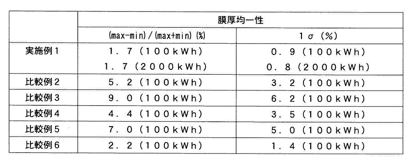
- the film thickness is measured at each point, and the film thickness at each point is calculated therefrom. From the maximum value (max) and the minimum value (min), according to the formula: (max ⁇ min) / (max + min) ⁇ 100 (%) The thickness uniformity was determined, and the film thickness uniformity of the thin film formed on each substrate was evaluated by each sputtering target.
- the film thickness was calculated from the sheet resistance value ( ⁇ / ⁇ ) measured at the above 49 points, the standard deviation ⁇ was calculated therefrom, and a value of 1 ⁇ % (percent 1 sigma) was calculated.
- the standard deviation ⁇ is calculated by the following equation.
- n the number of data
- X AVE represents an average value
- the standard-shaped sputtering target of the reference example (target material T 0 (see FIG. 4)) is excellent in film thickness uniformity, but its lifetime is 1200 kWh. It was not satisfactory.
- the standard-shaped sputtering target of the reference example can ensure a certain degree of film thickness uniformity over the entire surface of the thin film formed on the substrate (that is, in all points 1 to 49). However, it turned out that the film thickness is low in the center part (Point 1).
- the sputtering target (target material T (see FIG. 2)) of Example 1 of the present invention has a long life of 2000 kWh. It was.
- the lifetime of the standard shape sputtering target of the reference example is 1200 kWh as described above (FIGS. 10 and 12), whereas the sputtering target of Example 1 of the present invention has the standard shape sputtering target of the reference example. It was found to have a lifetime of 1.5 times or more of the target.
- the film thickness uniformity superior to that of the above-mentioned reference-shaped sputtering target in the entire range of 0 to 2000 kWh is exhibited. I understood.
- the sputtering target of Example 1 of the present invention has a long lifetime of 2000 kWh and can provide excellent film thickness uniformity over the entire surface of the substrate in the entire lifetime of 0 to 2000 kWh. .
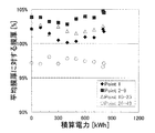
- the sputtering target of Comparative Example 1 can perform sputtering up to 2000 kWh. It was found that the film thickness uniformity was significantly deteriorated at 0 to 300 kWh.
- the film thickness is small in the central portion (Point 1) of the substrate, and particularly in the initial stage (0 to 300 kWh), the central portion (Point 1) of the substrate. It was found that the film thickness was extremely small.
- the film thickness uniformity is poor at the initial stage of sputtering (0 to 300 kWh). It was found that the film thickness was extremely small at the center (Point 1).
- the film thickness of the thin film formed on the outer peripheral portion (Point 26-49) of the substrate is small from the initial stage immediately after sputtering, and is uniform over the entire surface of the substrate. It was found that a sufficient film thickness could not be obtained.
- the film thickness uniformity is improved from the initial stage of sputtering. It turned out to be significantly worse.
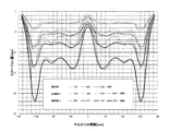
- FIG. 18 shows the amount of erosion of the target material in the sputtering target of Comparative Example 2.
- the solid line shows the erosion amount of the target material of the sputtering target of the reference example
- the broken line shows the erosion amount of the target material of the sputtering target of Comparative Example 2 (every 400 kWh from 0 to 800 kWh).
- FIG. 18 indicates that the most consumed portion of the target material is closer to the outer peripheral portion in the sputtering target of Comparative Example 2 than in the reference example.
- the amount of sputtering at a position farther from the outer periphery of the substrate increases and is consumed without reaching the outer periphery (Point 26-49) of the substrate, so that at the outer periphery of the substrate (Point 26-49) The film thickness decreases. This is consistent with the results shown in the graph of FIG.
- the sputtering target of Comparative Example 6 has a first region diameter of 32.6% of the outer peripheral diameter of the sputtering surface. It was found that the film thickness uniformity deteriorated as compared with Example 1 in which the diameter of this region was 70.2% of the outer diameter of the sputtering surface.
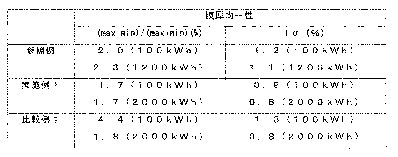
- Example 1 of the present invention even when compared with Reference Example and Comparative Example 1, it can be seen that the film thickness uniformity is dramatically improved both in the initial stage and in the long term, particularly in the initial stage.
- the values of 1 ⁇ at 100 kWh are 1.2% (reference example) and 1.3% (comparative example 1), respectively, and in any case, the film thickness uniformity is Looks good.
- Comparative Example 1 the film thickness uniformity in the initial stage (0 to 300 kWh) is extremely poor as described with reference to FIGS. 14 and 15 described above, and in particular, as shown in FIG. Among the 49 points measured at 0 to 300 kWh), only the film thickness at the center point (Point 1) was extremely low. Such a result is because the film thickness at the center point (Point 1) is hardly reflected in the calculation of 1 ⁇ , and from the value of 1 ⁇ , it appears that the film thickness uniformity is apparently good. . Therefore, it was found that it is not very appropriate to evaluate the film thickness uniformity by the value of 1 ⁇ .
- Example 1 -Examination of lifetime improvement based on erosion amount of target material
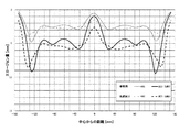
- the erosion amount of the target material measured about each sputtering target of the reference example, the comparative example 1, and Example 1 is shown in FIG.
- the broken line indicates erosion in the reference example
- the dotted line indicates erosion in Comparative Example 1
- the solid line indicates erosion in Example 1 (400 to 2000 kWh, 400, 800, 1200 and 2000 kWh, where Reference examples are up to 1200 kWh).
- the portion from 70 to 125 mm from the center, particularly from around 90 mm from the center that is, 56.4% relative to the radius of the sputtering surface of 159.57 mm. It was found that the erosion increased in the vicinity of 125 mm (78.3% with respect to the sputtering surface radius of 159.57 mm).
- Comparative Example 4 target material Tc 4
- Comparative Example 3 target material Tc 3
- the central portion of the sputtering surface is flat over a certain range, preferably as described above, over the range of 60% to 80% of the outer diameter of the sputtering surface (see FIG. 19), in the initial stage of sputtering. It was found that the film thickness uniformity can be improved by increasing the film thickness of the central part (Point 1) of the thin film formed on the substrate.
- results shown in FIGS. 20 and 21 described above show that there is some correlation between the thickness of the central portion of the sputtering target and the thickness of the central portion (Point 1) of the thin film formed on the substrate. Suggests.
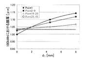
- the results shown in FIG. 22 reveal that the film thickness at each point converges and the film thickness uniformity improves as the value of d 1 decreases from 8 mm.
- the film thickness uniformity is significantly improved when d 1 is 4.0 mm or less, particularly 1.65 mm.
- the value of d 1 is preferably set to 4.0 mm or less (the first region is therefore located at a position that is at most 15% lower than the thickness of the second region with respect to the second region).
- the film thickness uniformity of the thin film formed on the substrate could be improved.
- the sputtering target of the present invention can be used in a commercially available sputtering apparatus, particularly a magnetron sputtering apparatus, provides a long life of 1800 kWh or more with integrated power, and in addition, a thin film having excellent film thickness uniformity. This is beneficial because it can be formed on a substrate.
Landscapes
- Chemical & Material Sciences (AREA)
- Engineering & Computer Science (AREA)
- Physics & Mathematics (AREA)
- Plasma & Fusion (AREA)
- Analytical Chemistry (AREA)
- Chemical Kinetics & Catalysis (AREA)
- Materials Engineering (AREA)
- Mechanical Engineering (AREA)
- Metallurgy (AREA)
- Organic Chemistry (AREA)
- Physical Vapour Deposition (AREA)
- Electrodes Of Semiconductors (AREA)
Abstract
Description
ターゲット材を含むスパッタリングターゲットであって、前記ターゲット材が、そのスパッタリング面において、中央に位置する円形の平坦な第1の領域と、前記第1の領域の外側に前記第1の領域と同心円状に配置されるリング状の第2の領域とを有し、前記第1の領域は、前記第2の領域に対して、最大で前記第2の領域の厚さの15%低い位置に配置されていて、前記第1の領域の直径が、前記スパッタリング面の外周の直径の60%~80%であることを特徴とする、スパッタリングターゲット。
[2]
前記第1の領域が、前記第2の領域に対して、前記第2の領域の厚さの4%~12%低い位置にあることを特徴とする、上記[1]に記載のスパッタリングターゲット。
[3]
前記ターゲット材における前記第1の領域の厚さが20mm~30mmであることを特徴とする、上記[1]または[2]に記載のスパッタリングターゲット。
[4]
前記ターゲット材における前記第2の領域の厚さが25mm~35mmであることを特徴とする、上記[1]~[3]のいずれか1項に記載のスパッタリングターゲット。
[5]
前記ターゲット材がその周縁部に段差を有していないことを特徴とする、上記[1]~[4]のいずれか1項に記載のスパッタリングターゲット。
[6]
前記ターゲット材がアルミニウムまたはアルミニウム合金から成ることを特徴とする、上記[1]~[5]のいずれか1項に記載のスパッタリングターゲット。
本発明のスパッタリングターゲットの一実施形態を図1および2に模式的に示す。なお、図1および2において示される本発明のスパッタリングターゲットは、例示のために模式的に示されるものであり、実際の寸法および形状は本明細書中に定義する通りである。
ターゲット材Tは、例えば、アルミニウム(Al)、クロム(Cr)、鉄(Fe)、タンタル(Ta)、チタン(Ti)、ジルコニウム(Zr)、タングステン(W)、モリブデン(Mo)、ニオブ(Nb)等の金属およびそれらの合金からなる群から選択される材料から作製することができるが、ターゲット材Tを構成する材料は、これらに限定されるものではない。
第1の領域1は、図2に示す通り、スパッタリング面Sの中央に位置していて、円形の平坦な形状を有する領域であり、第2の領域2よりも低い位置(垂直下方)に配置されるものである。
第2の領域2は、図2に示す通り、第1の領域の外側にあり、第1の領域と同心円状に配置されるリング状の領域である。
図2に示す実施形態では、第1の領域1と第2の領域2との間に中間領域3が存在する。中間領域3は、第1の領域1と第2の領域2とを連続的に接続するものであり、好ましくは第1の領域1と第2の領域2とを直線的に接続するものである。
図1および2に示すように、本発明のスパッタリングターゲット10は、上述のターゲット材Tを載置して、例えばマグネトロンスパッタリング装置などのスパッタリング装置に固定するための支持部材6を更に含んでいてもよい。
本発明のスパッタリングターゲットの製造方法では、例えば、まず、ターゲット材Tの材料を混合して溶融して鋳造することにより、スラブと呼ばれる鋳塊を形成し、かかる鋳塊を圧延して熱処理した後に任意の寸法で円盤状にくり抜き、ターゲット材の予備成形体を得る。
本発明のスパッタリングターゲットを使用することのできるスパッタリング装置に特に制限はなく、市販のスパッタリング装置を何ら制限なく使用することができる。
本発明のスパッタリングターゲットおよび上述のスパッタリング装置を使用して、その上に薄膜を形成することのできる基板としては、特に制限はなく、例えば、シリコン、銅等の金属ウエハや、酸化亜鉛、酸化マグネシウム等の酸化物ウエハ、石英、パイレックス等のガラス基板や、樹脂基板などを使用することができる。
本発明のスパッタリングターゲットは、積算電力で1800kWh以上、好ましくは2000kWh以上の長寿命を有する。これは、従来の標準形状のターゲット材を有するスパッタリングターゲットの寿命(1200kWh)の1.5倍以上である。
本発明のスパッタリングターゲットによって基板上に形成される薄膜の膜厚均一性は、基板上に形成される薄膜の所定の49点にて測定した薄膜のシート抵抗値RS(Ω/□)と、既知の薄膜の体積抵抗率RV(Ω・m)とにより、式:t=RV/RS×106から求められる膜厚t(μm)の値の最大値(max)と最小値(min)とに基づいて、式:(max-min)/(max+min)×100(%)から求めることができる。なお、アルミニウム薄膜の場合、RV=2.9×10-8(Ω・m)である。
純度99.999%以上のアルミニウムに、0.5重量%の銅を添加し、これらの混合物を溶融して鋳造して得られる鋳塊(スラブ)を圧延して熱処理した後に円盤状にくり抜き、ターゲット材の予備成形体を得た。
r1:112.00mm
d1:1.65mm(第2の領域2の厚さd3の5.98%)
d2:23.94mm
d3:27.60mm
d4:319.14mm
d5:44.57mm
d6:3.00mm
θ:29°
r1/rs:70.2%
スパッタリングターゲット全体の高さ(第2の領域の上面から支持部材のフランジ部の裏面までの距離):56.26mm
実施例1と同様にして、図3に示す標準形状のターゲット材T0を備えたスパッタリングターゲットを作製した。なお、ターゲット材T0の支持部材は、実施例1と同一形状のものを使用した。
ターゲット材T0の接合部xを除く最大厚さd0:19.61mm
スパッタリングターゲット全体の高さ(ターゲット材T0の上面から支持部材のフランジ部の裏面までの距離):48.26mm
実施例1と同様にして、図4の断面図および図6の上面図に示す形状のターゲット材Tc1を備えたスパッタリングターゲットを作製した。なお、ターゲット材Tc1の支持部材は、実施例1と同一形状のものを使用した。
d0:19.61mm
d10:8.00mm
スパッタリング面の直径(平面領域101の直径)d11:319.14mm
スパッタリングターゲット全体の高さ(ターゲット材TC1の上面から支持部材のフランジ部の裏面までの距離):56.26mm
実施例1と同様にして、図4の断面図および図6の上面図に示す形状のターゲット材Tc2を備えたスパッタリングターゲットを作製した。なお、ターゲット材Tc2の支持部材は、実施例1と同一の形状のものを使用した。
d0:19.61mm
d10:8.00mm
d12(中心平面領域102の直径):260.00mm
d13(段差部の幅):16.71mm
d14(傾斜部の幅):15.00mm
スパッタリングターゲット全体の高さ(ターゲット材Tc2の最上面から支持部材のフランジ部の裏面までの距離):56.26mm
実施例1と同様にして、図5の断面図および図7の上面図に示す形状のターゲット材Tc3を備えたスパッタリングターゲットを作製した。なお、ターゲット材Tc3の支持部材は、実施例1と同一形状のものを使用した。
d15(リングの高さ):8.00mm(ターゲット材の厚さ(d0+d15)の29.0%)
d16(中心平面領域103の直径):200.00mm
d17(リング状の平面領域201のリング幅):15.00mm
d18(リングの内側の傾斜部の幅):15.00mm
d19(リングの外側の傾斜部の幅):15.00mm
d20(段差部の幅):16.71mm
スパッタリングターゲット全体の高さ(ターゲット材Tc3の最上面から支持部材のフランジ部の裏面までの距離):56.26mm
実施例1と同様にして、図5の断面図および図7の上面図に示す形状のターゲット材Tc4を備えたスパッタリングターゲットを作製した。なお、ターゲット材Tc4の支持部材は、実施例1と同一形状のものを使用した。
d21(内側リングの高さ):8.00mm(ターゲット材の厚さ(d0+d21(=d0+d22))の29.0%)
d22(外側リングの高さ):8.00mm(ターゲット材の厚さ(d0+d21(=d0+d22))の29.0%)
d23(中心平面領域104の直径):10.00mm
d24(内側リングのリング幅):20.00mm
d25(内側リングの内側傾斜部の幅):15.00mm
d26(内側リングの外側傾斜部の幅):15.00mm
d27(外側リングのリング幅):15.00mm
d28(外側リングの内側傾斜部の幅):15.00mm
d29(外側リングの外側傾斜部の幅):15.00mm
d30(段差部の幅):16.71mm
d31(外側平面領域105の幅):45.00mm
スパッタリングターゲット全体の高さ(ターゲット材TC4の最上面から支持部材のフランジ部の裏面までの距離):56.26mm
実施例1と同様にして、図8の上面図および断面図に示す形状のターゲット材Tc5を備えたスパッタリングターゲットを作製した。なお、ターゲット材Tc5の支持部材は、実施例1と同一形状のものを使用した。
r1:105.00mm
d1:4.49mm(第2の領域の厚さd3の16.3%)
d2:21.11mm
d3:27.60mm
d4:323.42mm
d5:15.00mm
d6:10.00mm
d7:15.00mm
d8:16.71mm
d9:19.61mm
θ:24°
r1/rs:64.9%
スパッタリングターゲット全体の高さ(第2の領域2の上面から支持部材のフランジ部の裏面までの距離):56.26mm
r1およびd5の寸法を変更したこと以外は、実施例1と同様にして、ターゲット材Tc6を備えたスパッタリングターゲットを作製した。なお、ターゲット材Tc6の支持部材は、実施例1と同一形状のものを使用した。
r1:52.00mm
d1:1.65mm(第2の領域2の厚さd3の5.98%)
d2:23.94mm
d3:27.60mm
d4:319.14mm
d5:104.57mm
d6:3.00mm
θ:29°
r1/rs:32.6%
スパッタリングターゲット全体の高さ(第2の領域の上面から支持部材のフランジ部の裏面までの距離):56.26mm
マグネトロンスパッタリング装置(アプライド・マテリアルズ社製のEndura 5500、マグネット:Dura-type)、ならびに実施例、参照例および比較例のスパッタリングターゲットをそれぞれ使用して、直径が200mmの基板(LG Siltron社製のシリコン基板)に、以下の条件にて、薄膜を形成した。
出力:10600W
不活性ガス:アルゴン
チャンバ内圧力:2.75mTorr
基板温度:300℃
ターゲット-基板間の距離(TS距離):35mm(ターゲット材:T、Tc1~Tc6)または43mm(ターゲット材:T0)
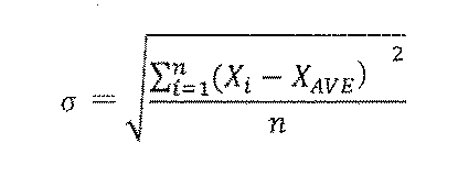
図10のグラフに示す通り、参照例の標準形状のスパッタリングターゲット(ターゲット材T0(図4参照))では、膜厚均一性に優れるが、その寿命は1200kWhであり、十分に満足できるものではなかった。
図12のグラフに示す通り、本発明の実施例1のスパッタリングターゲット(ターゲット材T(図2参照))では、2000kWhの長寿命を有することが明らかとなった。なお、参照例の標準形状のスパッタリングターゲットの寿命は、上述の通り1200kWhであり(図10および12)、これに対して、本発明の実施例1のスパッタリングターゲットは、参照例の標準形状のスパッタリングターゲットの1.5倍以上の寿命を有することがわかった。
図14に示す通り、比較例1のスパッタリングターゲット(ターゲット材Tc1(図4参照))では、2000kWhまでスパッタリングを行うことはできるが、その初期段階、特に0~300kWhにおいて、膜厚均一性が著しく悪化することがわかった。
図16に示す通り、比較例2のスパッタリングターゲット(ターゲット材Tc2(図4参照))は、スパッタリングの直後の初期段階から、膜厚均一性が著しく悪化することがわかった。
以下の表に示す通り、比較例3、4および5のスパッタリングターゲットは、いずれも初期段階(特に100kWh)での膜厚均一性が著しく悪いことが明らかとなった。
以下の表に示す通り、比較例6のスパッタリングターゲットは、第1の領域の直径がスパッタリング面の外周の直径の32.6%であることから、第1の領域の直径がスパッタリング面の外周の直径の70.2%である実施例1に比べると、膜厚均一性が悪化することがわかった。
ここで、ターゲット材の周縁部に段差のない参照例(図3、ターゲット材T0参照)、本発明の実施例1(図3、ターゲット材T参照)および比較例1(図4、ターゲット材Tc1参照)について、膜厚均一性の結果を以下の表にまとめる(図10、12および14の結果もあわせて参照のこと)。
参照例、比較例1および実施例1の各スパッタリングターゲットについて測定したターゲット材のエロージョン量を図19に示す。破線は、参照例でのエロージョンを示し、点線は、比較例1でのエロージョンを示し、実線は、実施例1でのエロージョンを示す(400~2000kWhで、400、800、1200および2000kWh、ただし、参照例は、1200kWhまで)。
2 第2の領域
3 第1の領域と第2の領域との間の中間領域
(または第2の領域の内側の周囲部)
4 ターゲット材の裏面(スパッタリング面の反対側の面)
5 ターゲット材の周縁部
6 支持部材
7 フランジ部
8 第2の領域の外側の周囲部
9 ターゲット材の周縁部に設けた段差部
10 本発明のスパッタリングターゲット
101 比較例1のスパッタリングターゲットのターゲット材Tc1の平面領域(スパッタリング面)
102 比較例2のスパッタリングターゲットのターゲット材Tc2の平面領域
103 比較例3のスパッタリングターゲットのターゲット材Tc3の中心平面領域
104 比較例4のスパッタリングターゲットのターゲット材Tc4の中心平面領域
105 比較例4のスパッタリングターゲットのターゲット材Tc4の外側平面領域
201 比較例3のスパッタリングターゲットのターゲット材Tc3のリング状の平面領域
202 比較例4のスパッタリングターゲットのターゲット材Tc4の二重リングの外側のリング状の平面領域
203 比較例4のスパッタリングターゲットのターゲット材Tc4の二重リングの内側のリング状の平面領域
S スパッタリング面
T ターゲット材
T0 標準形状のターゲット材
Tc1~Tc6 比較例1~6のスパッタリングターゲットのターゲット材
x ターゲット材の支持部材との接合部
Claims (6)
- ターゲット材を含むスパッタリングターゲットであって、前記ターゲット材が、そのスパッタリング面において、中央に位置する円形の平坦な第1の領域と、前記第1の領域の外側に前記第1の領域と同心円状に配置されるリング状の第2の領域とを有し、前記第1の領域は、前記第2の領域に対して、最大で前記第2の領域の厚さの15%低い位置に配置されていて、前記第1の領域の直径が、前記スパッタリング面の外周の直径の60%~80%であることを特徴とする、スパッタリングターゲット。
- 前記第1の領域が、前記第2の領域に対して、前記第2の領域の厚さの4%~12%低い位置にあることを特徴とする、請求項1に記載のスパッタリングターゲット。
- 前記ターゲット材における前記第1の領域の厚さが20mm~30mmであることを特徴とする、請求項1または2に記載のスパッタリングターゲット。
- 前記ターゲット材における前記第2の領域の厚さが25mm~35mmであることを特徴とする、請求項1~3のいずれか1項に記載のスパッタリングターゲット。
- 前記ターゲット材がその周縁部に段差を有していないことを特徴とする、請求項1~4のいずれか1項に記載のスパッタリングターゲット。
- 前記ターゲット材がアルミニウムまたはアルミニウム合金から成ることを特徴とする、請求項1~5のいずれか1項に記載のスパッタリングターゲット。
Priority Applications (7)
| Application Number | Priority Date | Filing Date | Title |
|---|---|---|---|
| JP2015558852A JP6203870B2 (ja) | 2014-01-21 | 2015-01-20 | スパッタリングターゲット |
| CN201580005170.1A CN105934533B (zh) | 2014-01-21 | 2015-01-20 | 溅射靶 |
| EP15741025.9A EP3098332B1 (en) | 2014-01-21 | 2015-01-20 | Sputtering target |
| US15/112,242 US11532468B2 (en) | 2014-01-21 | 2015-01-20 | Sputtering target |
| KR1020217013891A KR20210055807A (ko) | 2014-01-21 | 2015-01-20 | 스퍼터링 타겟 |
| KR1020167019560A KR20160111387A (ko) | 2014-01-21 | 2015-01-20 | 스퍼터링 타겟 |
| IL246811A IL246811B (en) | 2014-01-21 | 2016-07-18 | A target for emitting power |
Applications Claiming Priority (2)
| Application Number | Priority Date | Filing Date | Title |
|---|---|---|---|
| JP2014008740 | 2014-01-21 | ||
| JP2014-008740 | 2014-01-21 |
Publications (1)
| Publication Number | Publication Date |
|---|---|
| WO2015111576A1 true WO2015111576A1 (ja) | 2015-07-30 |
Family
ID=53681379
Family Applications (1)
| Application Number | Title | Priority Date | Filing Date |
|---|---|---|---|
| PCT/JP2015/051395 Ceased WO2015111576A1 (ja) | 2014-01-21 | 2015-01-20 | スパッタリングターゲット |
Country Status (9)
| Country | Link |
|---|---|
| US (1) | US11532468B2 (ja) |
| EP (1) | EP3098332B1 (ja) |
| JP (3) | JP6203870B2 (ja) |
| KR (2) | KR20160111387A (ja) |
| CN (1) | CN105934533B (ja) |
| IL (1) | IL246811B (ja) |
| MY (1) | MY180359A (ja) |
| TW (1) | TWI678424B (ja) |
| WO (1) | WO2015111576A1 (ja) |
Cited By (2)
| Publication number | Priority date | Publication date | Assignee | Title |
|---|---|---|---|---|
| CN105154836A (zh) * | 2015-09-18 | 2015-12-16 | 有研亿金新材料有限公司 | 一种高性能铁磁性溅射靶材 |
| US11862443B2 (en) * | 2017-03-29 | 2024-01-02 | Sumitomo Chemical Company, Limited | Sputtering target |
Families Citing this family (7)
| Publication number | Priority date | Publication date | Assignee | Title |
|---|---|---|---|---|
| CN106683988B (zh) * | 2016-12-28 | 2019-05-24 | 惠科股份有限公司 | 一种靶材装置 |
| CN110010455A (zh) * | 2018-01-04 | 2019-07-12 | 合肥江丰电子材料有限公司 | 长寿命lcd靶材组件及其形成方法 |
| CN110029316A (zh) * | 2018-01-11 | 2019-07-19 | 合肥江丰电子材料有限公司 | 长寿命lcd靶材组件及其形成方法 |
| CN108624856B (zh) * | 2018-07-05 | 2024-06-25 | 包头稀土研究院 | 靶材组件 |
| CN109055900B (zh) * | 2018-09-17 | 2020-10-02 | 中国科学院宁波材料技术与工程研究所 | 一种用于阴极电弧沉积的复合靶及沉积方法 |
| CN110592406A (zh) * | 2019-10-10 | 2019-12-20 | 新疆众和股份有限公司 | 一种溅射用高纯铝铜合金靶材坯料的制备方法 |
| JP7511419B2 (ja) * | 2020-09-09 | 2024-07-05 | 東京エレクトロン株式会社 | 成膜方法、成膜装置及びプログラム |
Citations (3)
| Publication number | Priority date | Publication date | Assignee | Title |
|---|---|---|---|---|
| JP2000265270A (ja) * | 1999-03-18 | 2000-09-26 | Anelva Corp | スパッタリング装置のマグネトロンカソード |
| JP4213030B2 (ja) | 2001-06-05 | 2009-01-21 | プラックセアー エス.ティ.テクノロジー、 インコーポレイテッド | リング型スパッタリング・ターゲット |
| JP2012522894A (ja) * | 2009-04-03 | 2012-09-27 | アプライド マテリアルズ インコーポレイテッド | Pvdチャンバ用スパッターターゲット |
Family Cites Families (20)
| Publication number | Priority date | Publication date | Assignee | Title |
|---|---|---|---|---|
| JPS4213030B1 (ja) | 1962-07-19 | 1967-07-25 | ||
| JPS61183467A (ja) * | 1985-02-08 | 1986-08-16 | Hitachi Ltd | スパッタリング方法及びその装置 |
| JPS637366A (ja) * | 1986-06-27 | 1988-01-13 | Matsushita Electric Ind Co Ltd | マグネトロンスパツタ装置 |
| JPH04213030A (ja) | 1990-11-22 | 1992-08-04 | Tepitsuku:Kk | 紫外線強度計 |
| JPH05287524A (ja) | 1992-04-09 | 1993-11-02 | Anelva Corp | マグネトロンスパッタリング用ターゲット |
| JP2917743B2 (ja) * | 1993-04-23 | 1999-07-12 | 三菱マテリアル株式会社 | マグネトロンスパッタリング用Siターゲット材 |
| JPH08325719A (ja) | 1995-05-29 | 1996-12-10 | Sony Corp | スパッタ装置 |
| JPH09111445A (ja) * | 1995-10-12 | 1997-04-28 | Dainippon Printing Co Ltd | スパッタリングターゲット |
| US6086735A (en) | 1998-06-01 | 2000-07-11 | Praxair S.T. Technology, Inc. | Contoured sputtering target |
| JP2001140063A (ja) | 1999-09-23 | 2001-05-22 | Praxair St Technol Inc | 延長された寿命を有するスパッタターゲット |
| US6497797B1 (en) | 2000-08-21 | 2002-12-24 | Honeywell International Inc. | Methods of forming sputtering targets, and sputtering targets formed thereby |
| WO2002042518A1 (de) * | 2000-11-27 | 2002-05-30 | Unaxis Trading Ag | Target mit dickenprofilierung für rf manetron |
| US6872284B2 (en) | 2001-04-24 | 2005-03-29 | Tosoh Smd, Inc. | Target and method of optimizing target profile |
| KR20040057287A (ko) | 2002-12-26 | 2004-07-02 | 삼성전자주식회사 | 스퍼터링용 타겟 |
| US6988306B2 (en) * | 2003-12-01 | 2006-01-24 | Praxair Technology, Inc. | High purity ferromagnetic sputter target, assembly and method of manufacturing same |
| JP2008038229A (ja) * | 2006-08-09 | 2008-02-21 | Mitsui Mining & Smelting Co Ltd | スパッタリング方法およびそれに用いられるスパッタリングターゲット |
| US20120097534A1 (en) * | 2008-08-29 | 2012-04-26 | Ulvac, Inc. | Magnetron sputtering cathode and film formation apparatus |
| CN201793723U (zh) * | 2010-09-28 | 2011-04-13 | 宁波江丰电子材料有限公司 | 一种长寿命溅射靶材 |
| CN105008582A (zh) * | 2013-01-04 | 2015-10-28 | 东曹Smd有限公司 | 具有增强的表面轮廓和改善的性能的硅溅射靶及其制造方法 |
| US9779920B2 (en) * | 2013-08-14 | 2017-10-03 | Applied Materials, Inc. | Sputtering target with backside cooling grooves |
-
2015
- 2015-01-20 KR KR1020167019560A patent/KR20160111387A/ko not_active Ceased
- 2015-01-20 KR KR1020217013891A patent/KR20210055807A/ko not_active Ceased
- 2015-01-20 JP JP2015558852A patent/JP6203870B2/ja active Active
- 2015-01-20 EP EP15741025.9A patent/EP3098332B1/en active Active
- 2015-01-20 MY MYPI2016702597A patent/MY180359A/en unknown
- 2015-01-20 WO PCT/JP2015/051395 patent/WO2015111576A1/ja not_active Ceased
- 2015-01-20 TW TW104101813A patent/TWI678424B/zh active
- 2015-01-20 US US15/112,242 patent/US11532468B2/en active Active
- 2015-01-20 CN CN201580005170.1A patent/CN105934533B/zh active Active
-
2016
- 2016-07-18 IL IL246811A patent/IL246811B/en active IP Right Grant
-
2017
- 2017-06-06 JP JP2017111872A patent/JP6271796B2/ja active Active
- 2017-12-27 JP JP2017251213A patent/JP6514763B2/ja active Active
Patent Citations (3)
| Publication number | Priority date | Publication date | Assignee | Title |
|---|---|---|---|---|
| JP2000265270A (ja) * | 1999-03-18 | 2000-09-26 | Anelva Corp | スパッタリング装置のマグネトロンカソード |
| JP4213030B2 (ja) | 2001-06-05 | 2009-01-21 | プラックセアー エス.ティ.テクノロジー、 インコーポレイテッド | リング型スパッタリング・ターゲット |
| JP2012522894A (ja) * | 2009-04-03 | 2012-09-27 | アプライド マテリアルズ インコーポレイテッド | Pvdチャンバ用スパッターターゲット |
Non-Patent Citations (1)
| Title |
|---|
| See also references of EP3098332A4 |
Cited By (2)
| Publication number | Priority date | Publication date | Assignee | Title |
|---|---|---|---|---|
| CN105154836A (zh) * | 2015-09-18 | 2015-12-16 | 有研亿金新材料有限公司 | 一种高性能铁磁性溅射靶材 |
| US11862443B2 (en) * | 2017-03-29 | 2024-01-02 | Sumitomo Chemical Company, Limited | Sputtering target |
Also Published As
| Publication number | Publication date |
|---|---|
| JP2017179609A (ja) | 2017-10-05 |
| JPWO2015111576A1 (ja) | 2017-03-23 |
| US20160343551A1 (en) | 2016-11-24 |
| JP2018076598A (ja) | 2018-05-17 |
| JP6203870B2 (ja) | 2017-09-27 |
| JP6271796B2 (ja) | 2018-01-31 |
| KR20210055807A (ko) | 2021-05-17 |
| MY180359A (en) | 2020-11-28 |
| IL246811B (en) | 2019-12-31 |
| KR20160111387A (ko) | 2016-09-26 |
| TW201540857A (zh) | 2015-11-01 |
| JP6514763B2 (ja) | 2019-05-15 |
| EP3098332A4 (en) | 2017-06-28 |
| TWI678424B (zh) | 2019-12-01 |
| EP3098332B1 (en) | 2019-10-16 |
| IL246811A0 (en) | 2016-08-31 |
| CN105934533B (zh) | 2018-11-27 |
| CN105934533A (zh) | 2016-09-07 |
| EP3098332A1 (en) | 2016-11-30 |
| US11532468B2 (en) | 2022-12-20 |
Similar Documents
| Publication | Publication Date | Title |
|---|---|---|
| JP6271796B2 (ja) | スパッタリングターゲット | |
| JP6077102B2 (ja) | スパッタリング用チタンターゲット及びその製造方法 | |
| TWI605142B (zh) | 具有增進的表面輪廓和改善的性能的矽濺射靶及製造其之方法 | |
| CN109599319B (zh) | 用于基板处理腔室的带鳍片的挡板盘 | |
| KR102338193B1 (ko) | 스퍼터링 타깃 | |
| JP5533545B2 (ja) | 有機el素子の反射電極膜形成用銀合金ターゲットおよびその製造方法 | |
| JP6498527B2 (ja) | スパッタリングターゲット | |
| JP2015025170A (ja) | シリコンターゲット |
Legal Events
| Date | Code | Title | Description |
|---|---|---|---|
| 121 | Ep: the epo has been informed by wipo that ep was designated in this application |
Ref document number: 15741025 Country of ref document: EP Kind code of ref document: A1 |
|
| ENP | Entry into the national phase |
Ref document number: 2015558852 Country of ref document: JP Kind code of ref document: A |
|
| WWE | Wipo information: entry into national phase |
Ref document number: 15112242 Country of ref document: US Ref document number: 246811 Country of ref document: IL |
|
| ENP | Entry into the national phase |
Ref document number: 20167019560 Country of ref document: KR Kind code of ref document: A |
|
| REEP | Request for entry into the european phase |
Ref document number: 2015741025 Country of ref document: EP |
|
| WWE | Wipo information: entry into national phase |
Ref document number: 2015741025 Country of ref document: EP |
|
| NENP | Non-entry into the national phase |
Ref country code: DE |