WO2015114787A1 - 半導体素子の駆動装置およびそれを用いた電力変換装置 - Google Patents
半導体素子の駆動装置およびそれを用いた電力変換装置 Download PDFInfo
- Publication number
- WO2015114787A1 WO2015114787A1 PCT/JP2014/052196 JP2014052196W WO2015114787A1 WO 2015114787 A1 WO2015114787 A1 WO 2015114787A1 JP 2014052196 W JP2014052196 W JP 2014052196W WO 2015114787 A1 WO2015114787 A1 WO 2015114787A1
- Authority
- WO
- WIPO (PCT)
- Prior art keywords
- layer
- semiconductor layer
- type
- semiconductor
- current
- Prior art date
- Legal status (The legal status is an assumption and is not a legal conclusion. Google has not performed a legal analysis and makes no representation as to the accuracy of the status listed.)
- Ceased
Links
Images


Classifications
-
- H—ELECTRICITY
- H10—SEMICONDUCTOR DEVICES; ELECTRIC SOLID-STATE DEVICES NOT OTHERWISE PROVIDED FOR
- H10D—INORGANIC ELECTRIC SEMICONDUCTOR DEVICES
- H10D12/00—Bipolar devices controlled by the field effect, e.g. insulated-gate bipolar transistors [IGBT]
- H10D12/211—Gated diodes
-
- H—ELECTRICITY
- H02—GENERATION; CONVERSION OR DISTRIBUTION OF ELECTRIC POWER
- H02M—APPARATUS FOR CONVERSION BETWEEN AC AND AC, BETWEEN AC AND DC, OR BETWEEN DC AND DC, AND FOR USE WITH MAINS OR SIMILAR POWER SUPPLY SYSTEMS; CONVERSION OF DC OR AC INPUT POWER INTO SURGE OUTPUT POWER; CONTROL OR REGULATION THEREOF
- H02M7/00—Conversion of AC power input into DC power output; Conversion of DC power input into AC power output
- H02M7/003—Constructional details, e.g. physical layout, assembly, wiring or busbar connections
-
- H—ELECTRICITY
- H02—GENERATION; CONVERSION OR DISTRIBUTION OF ELECTRIC POWER
- H02M—APPARATUS FOR CONVERSION BETWEEN AC AND AC, BETWEEN AC AND DC, OR BETWEEN DC AND DC, AND FOR USE WITH MAINS OR SIMILAR POWER SUPPLY SYSTEMS; CONVERSION OF DC OR AC INPUT POWER INTO SURGE OUTPUT POWER; CONTROL OR REGULATION THEREOF
- H02M7/00—Conversion of AC power input into DC power output; Conversion of DC power input into AC power output
- H02M7/42—Conversion of DC power input into AC power output without possibility of reversal
- H02M7/44—Conversion of DC power input into AC power output without possibility of reversal by static converters
-
- H—ELECTRICITY
- H03—ELECTRONIC CIRCUITRY
- H03K—PULSE TECHNIQUE
- H03K17/00—Electronic switching or gating, i.e. not by contact-making and –breaking
- H03K17/16—Modifications for eliminating interference voltages or currents
- H03K17/161—Modifications for eliminating interference voltages or currents in field-effect transistor switches
- H03K17/162—Modifications for eliminating interference voltages or currents in field-effect transistor switches without feedback from the output circuit to the control circuit
-
- H—ELECTRICITY
- H03—ELECTRONIC CIRCUITRY
- H03K—PULSE TECHNIQUE
- H03K17/00—Electronic switching or gating, i.e. not by contact-making and –breaking
- H03K17/51—Electronic switching or gating, i.e. not by contact-making and –breaking characterised by the components used
- H03K17/74—Electronic switching or gating, i.e. not by contact-making and –breaking characterised by the components used by the use, as active elements, of diodes
-
- H—ELECTRICITY
- H10—SEMICONDUCTOR DEVICES; ELECTRIC SOLID-STATE DEVICES NOT OTHERWISE PROVIDED FOR
- H10D—INORGANIC ELECTRIC SEMICONDUCTOR DEVICES
- H10D12/00—Bipolar devices controlled by the field effect, e.g. insulated-gate bipolar transistors [IGBT]
- H10D12/411—Insulated-gate bipolar transistors [IGBT]
- H10D12/441—Vertical IGBTs
- H10D12/461—Vertical IGBTs having non-planar surfaces, e.g. having trenches, recesses or pillars in the surfaces of the emitter, base or collector regions
- H10D12/481—Vertical IGBTs having non-planar surfaces, e.g. having trenches, recesses or pillars in the surfaces of the emitter, base or collector regions having gate structures on slanted surfaces, on vertical surfaces, or in grooves, e.g. trench gate IGBTs
-
- H—ELECTRICITY
- H10—SEMICONDUCTOR DEVICES; ELECTRIC SOLID-STATE DEVICES NOT OTHERWISE PROVIDED FOR
- H10D—INORGANIC ELECTRIC SEMICONDUCTOR DEVICES
- H10D62/00—Semiconductor bodies, or regions thereof, of devices having potential barriers
- H10D62/10—Shapes, relative sizes or dispositions of the regions of the semiconductor bodies; Shapes of the semiconductor bodies
- H10D62/13—Semiconductor regions connected to electrodes carrying current to be rectified, amplified or switched, e.g. source or drain regions
- H10D62/141—Anode or cathode regions of thyristors; Collector or emitter regions of gated bipolar-mode devices, e.g. of IGBTs
-
- H—ELECTRICITY
- H10—SEMICONDUCTOR DEVICES; ELECTRIC SOLID-STATE DEVICES NOT OTHERWISE PROVIDED FOR
- H10D—INORGANIC ELECTRIC SEMICONDUCTOR DEVICES
- H10D62/00—Semiconductor bodies, or regions thereof, of devices having potential barriers
- H10D62/10—Shapes, relative sizes or dispositions of the regions of the semiconductor bodies; Shapes of the semiconductor bodies
- H10D62/13—Semiconductor regions connected to electrodes carrying current to be rectified, amplified or switched, e.g. source or drain regions
- H10D62/149—Source or drain regions of field-effect devices
- H10D62/151—Source or drain regions of field-effect devices of IGFETs
-
- H—ELECTRICITY
- H10—SEMICONDUCTOR DEVICES; ELECTRIC SOLID-STATE DEVICES NOT OTHERWISE PROVIDED FOR
- H10D—INORGANIC ELECTRIC SEMICONDUCTOR DEVICES
- H10D84/00—Integrated devices formed in or on semiconductor substrates that comprise only semiconducting layers, e.g. on Si wafers or on GaAs-on-Si wafers
- H10D84/60—Integrated devices formed in or on semiconductor substrates that comprise only semiconducting layers, e.g. on Si wafers or on GaAs-on-Si wafers characterised by the integration of at least one component covered by groups H10D10/00 or H10D18/00, e.g. integration of BJTs
- H10D84/611—Combinations of BJTs and one or more of diodes, resistors or capacitors
- H10D84/613—Combinations of vertical BJTs and one or more of diodes, resistors or capacitors
- H10D84/617—Combinations of vertical BJTs and only diodes
-
- H—ELECTRICITY
- H03—ELECTRONIC CIRCUITRY
- H03K—PULSE TECHNIQUE
- H03K2217/00—Indexing scheme related to electronic switching or gating, i.e. not by contact-making or -breaking covered by H03K17/00
- H03K2217/0036—Means reducing energy consumption
Definitions
- the present invention relates to a semiconductor device and a power conversion device using the same, and is particularly suitable for a device widely used from a low power device such as an air conditioner or a microwave oven to a high power device such as an inverter of a railway or a steelworks.
- the present invention relates to a semiconductor element driving device and a power conversion device using the same.
- Non-Patent Document 1 a mechanism of vibration generation due to a decrease in charge on the cathode side is known (see, for example, Non-Patent Document 1 and Non-Patent Document 2).
- FIG. 18 shows an example of an inverter that performs variable speed control of the motor 950 to realize energy saving.
- Electric energy from the power source 960 is changed to alternating current of a desired frequency by using an IGBT (Insulated Gate Bipolar Transistor) 700 which is a kind of power semiconductor, and the rotational speed of the motor 950 is controlled at a variable speed.
- the motor 950 is a three-phase motor and has inputs of a U-phase 910, a V-phase 911, and a W-phase 912.
- the input power of the U-phase 910 is supplied when the gate circuit 800 of the IGBT 700 (hereinafter referred to as the upper arm IGBT) whose collector is connected to the power terminal 900 on the plus side is turned on.
- gate circuit 800 may be turned off. By repeating this, electric power having a desired frequency can be supplied to the motor 950.
- the flywheel diode 600 is connected to the IGBT 700 in antiparallel with the IGBT 700.
- the flywheel diode 600 is configured such that the current flowing in the IGBT 700 is the IGBT 700 whose emitter is connected to the negative power supply terminal 901 (hereinafter referred to as the lower arm IGBT).
- the energy stored in the coil of the motor 950 is released by commutation to the antiparallel flywheel diode 600.
- the lower arm flywheel diode 600 is turned off, and power is supplied to the motor 950 through the upper arm IGBT 700.
- the IGBT 700 and the flywheel diode 600 Since the IGBT 700 and the flywheel diode 600 generate conduction loss when conducting, and switching occurs when switching, it is necessary to reduce the conduction loss and switching loss of the IGBT 700 and flywheel diode 600 in order to reduce the size and increase the efficiency of the inverter. There is.
- Patent Literature 1 and Patent Literature 2 have been reported as techniques for reducing conduction loss and recovery loss of the flywheel diode 600.
- Patent Document 1 describes a structure in which a MOS gate is provided on the anode side (FIGS. 1 to 5 in Patent Document 1) and a structure in which a MOS gate is provided on the cathode side (FIGS. 6 and 7 in Patent Document 1).
- the present invention relates to a structure in which a MOS gate is provided on the cathode side.
- Patent Document 1 describes that since the electron injection from the cathode can be controlled by the buried insulating gate, the trade-off between the forward voltage and the recovery loss can be improved.
- Patent Documents 1 and 2 described above have the following problems.
- the invention disclosed as an example in Patent Document 1 applies a positive voltage to the gate during conduction, and forms an electron storage layer. Reduce.
- the recovery loss is reduced by reducing the electron injection from the cathode by reducing the gate voltage to zero during recovery.
- a semiconductor device driving apparatus includes, for example, a first conductive type first semiconductor layer (n ⁇ type drift layer), one main surface adjacent to the first semiconductor layer, and the like.
- a second conductive type second semiconductor layer (p-type anode layer) exposed on the (anode side), adjacent to the first semiconductor layer, and exposed on the other main surface (cathode side) of the first conductivity type.
- a semiconductor device driving apparatus comprising a third semiconductor layer (n-type cathode layer) having an impurity concentration higher than that of the first semiconductor layer (n-type drift layer) and an insulating gate provided on the other main surface (cathode side)
- the insulated gate is switched from a positive voltage to a negative voltage immediately before recovery, and when the anode current is small, the insulated gate is held at a positive voltage.
- the power conversion device of the present invention is connected, for example, between a pair of DC terminals, an AC terminal having the same number of AC phases, and the pair of DC terminals, and each of a switching element and a diode having a reverse polarity. It comprises a configuration in which two parallel circuits are connected in series, and includes the same number of power conversion units as the number of AC phases connected to different AC terminals at different interconnection points of the parallel circuit, and the diode driving device comprises: It is a driving device of the semiconductor element described above.
- a low-loss and low-noise diode can be provided, so that the semiconductor device and the power converter can be improved in efficiency, size, and cost.
- the drive sequence of the insulated gate voltage during recovery is switched according to the magnitude of the anode current.
- Example 1 of the present invention (representative cross-sectional structure and driving method of the present invention) will be described below.
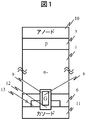
- FIG. 1 is a cross-sectional view of a first embodiment of a semiconductor device of the present invention.
- the n ⁇ type drift layer 1, the p type anode layer 3, the n type cathode layer 6, the gate electrode 8, the gate insulating film 9, the anode electrode 10, the cathode electrode 11, the insulating film 12, and the p + type cathode layer are used. 13.
- “+” indicates that the impurity concentration is high
- ⁇ indicates that the impurity concentration is low.
- the gate electrode 8 is set to a negative voltage with respect to the cathode electrode 11, thereby forming a p-type inversion layer at the interface between the gate electrode 8 and the n-type cathode layer 6 and injecting from the p-type anode layer 3. Promoted to be discharged to the cathode electrode 11 to reduce recovery loss.
- FIG. 2 shows the hole density distribution between the anode and the cathode during conduction.
- Vg 0V in the figure
- Vg + 15V in the figure
- a p-type inversion layer is formed at the interface between the gate electrode 8 and the n-type cathode layer 6, and holes injected from the p-type anode layer 3 are discharged to the cathode electrode 11 through the p-type inversion layer. This is because that.
- the gate electrode is set to a positive voltage (+ 15V in the figure)
- the current path via the p-type inversion layer disappears and an n-type accumulation layer is formed, so that hole discharge is suppressed and the hole density on the cathode side is reduced. Will increase.
- the absolute value of the gate negative voltage does not necessarily need to exceed the “threshold value (absolute value)” of the n-type cathode layer 6. Even if the absolute value of the voltage is lower than the “threshold value (absolute value)”, the potential of the channel with respect to the hole is lowered, so that the hole flows through the channel path with the lowered potential to the cathode electrode 11 and the hole from the cathode. Emissions are promoted.
- FIG. 3 shows output characteristics when positive voltage, zero volt, and negative voltage are applied to the gate electrode 8.
- Vf small forward voltage
- Vf large forward voltage
- FIG. 4 shows the relationship between the forward voltage (Vf) and the recovery loss (Err).
- the dotted line corresponds to a conventional pin diode.
- the gate voltage is dynamically controlled in one switching period, thereby minimizing each of the forward voltage (Vf) and the recovery loss (Err), thereby improving the trade-off characteristics.
- Patent Document 1 and Patent Document 2 the trade-off between the forward voltage (Vf) and the recovery loss (Err) is improved, and the loss can be significantly reduced.
- the inventors of the present application have evaluated the recovery characteristics of known examples under a condition where the anode current is small, and found that there is a problem that the voltage and current vibrate. Voltage and current oscillations became more pronounced at room temperature than at high temperature.
- the hole density on the cathode side is reduced immediately before the recovery in order to reduce the recovery loss, so that the depletion layer on the cathode side is easily extended.
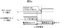
- FIG. 5a and 5b show the first gate drive sequence of this embodiment.
- FIG. 5a is a sequence in which the anode current is a rated current
- FIG. 5b is a sequence in which the anode current is a small current.
- it is difficult to quantitatively define a small current, it is generally about 1/10 or less to 1/2 or less of the rated current.
- the hole density on the cathode side is kept high by maintaining the gate of the MOS control diode at a positive voltage (high charge injection mode).
- the recovery loss is increased as compared with the low charge injection (high speed) mode, but the recovery loss of the small current is compared with the large current. Because it is small, the increase in recovery loss is negligible. That is, the merit (vibration suppression) of the present invention exceeds the demerit (increased loss).
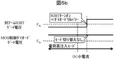
- FIG. 6a and 6b show waveforms of the anode current and the anode voltage during the small current recovery.
- FIG. 6a shows a conventional gate drive method for a MOS control diode in which the gate is switched from a positive voltage (high charge injection mode) to a negative voltage (low charge injection mode)
- FIG. 6b shows a gate drive for the MOS control diode of the present invention.
- the gate is held at a positive voltage (high charge injection mode).
- the anode current sharply decreases during the tail current period, and oscillations occur in the anode current and the anode voltage. On the other hand, in the present invention, such vibration does not occur.
- FIG. 7 shows a second gate drive sequence of the present invention.
- the gate of the MOS control diode maintained a positive voltage (high charge injection mode) over the recovery period, whereas in FIG. 7, the anode voltage decreased.
- the gate is switched to a negative voltage (low charge injection mode).
- a negative voltage is applied to the gate electrode while the cathode voltage is high and a p-type inversion layer is formed at the interface between the gate electrode 8 and the n-type cathode layer 6, holes are injected from the p + -type cathode layer 13 and the anode current is increased. And the oscillation of the anode voltage is suppressed.
- Example 2 of the present invention cross-sectional structure of a semiconductor element having no cathode-side p layer
- FIG. 8 is a cross-sectional view of a second embodiment of the semiconductor element of the present invention.
- This embodiment is different from the first embodiment in that there is no p + -type cathode layer 13.
- the gate electrode 8 when conducting, is set to a positive voltage with respect to the cathode electrode 11 to form an n-type accumulation layer at the interface between the gate electrode 8 and the n-type cathode layer 6, and the p-type anode layer 3.
- Vf forward voltage
- the gate electrode 8 is set to a negative voltage with respect to the cathode electrode 11 to form a p-type inversion layer at the interface between the gate electrode 8 and the n-type cathode layer 6 and injected from the p-type anode layer 3. This facilitates the discharge of the generated holes to the cathode electrode 11 and reduces the recovery loss.
- the oscillation of the anode voltage and the anode current can be suppressed by controlling the gate voltage of the MOS control diode according to the anode current.
- Example 3 of the present invention (a cross-sectional structure of a semiconductor element in which no p-layer on the cathode side and the gate electrode projects to the cathode electrode side) will be described below.
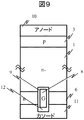
- FIG. 9 is a cross-sectional view of a third embodiment of the semiconductor element of the present invention.
- This embodiment differs from the second embodiment in that the gate electrode 8 on the cathode electrode 11 side is above the surface of the n-type cathode layer 6 (downward in the vertical direction in the figure).
- the gate electrode 8 covers the n-type cathode layer 6 in the depth direction, the gate electrode 8 can easily control the potential of the n-type cathode layer 6, loss reduction, Vibration can be suppressed.
- the oscillation of the anode voltage and the anode current can be suppressed by controlling the gate voltage of the MOS control diode according to the anode current.
- Example 4 of the present invention planar structure of a planar gate semiconductor device
- FIG. 10 is a cross-sectional view of the fourth embodiment of the semiconductor element of the present invention.
- This embodiment differs from the first embodiment in that the gate electrode 8 is not a trench type but a planar type. Similar to the first embodiment, this embodiment can also reduce loss and suppress vibration.
- the oscillation of the anode voltage and the anode current can be suppressed by controlling the gate voltage of the MOS control diode according to the anode current.
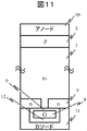
- Embodiment 5 of the present invention (planar structure of a semiconductor element having a planar gate type and no cathode-side p layer) will be described below.
- FIG. 11 is a cross-sectional view of a fifth embodiment of the semiconductor element of the present invention.
- This embodiment differs from the fourth embodiment in that there is no p + -type cathode layer 13. Similar to the fourth embodiment, this embodiment can also reduce loss and suppress voltage oscillation.
- the oscillation of the anode voltage and the anode current can be suppressed by controlling the gate voltage of the MOS control diode according to the anode current.
- Example 6 cross-sectional structure of an IGBT semiconductor element of the present invention will be described below.
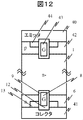
- FIG. 12 is a cross-sectional view of a sixth embodiment of the semiconductor element of the present invention.
- the structure on the collector side (rear surface) is the same as that on the cathode side (rear surface) of the first embodiment.
- the difference from the first embodiment is that a gate electrode 43 is provided on the emitter side.
- the n ⁇ type drift layer 1, the n type collector layer 6, the gate electrode 8, the gate insulating film 9, the insulating film 12, the p + type cathode layer 13, the emitter electrode 40, the collector electrode 41, and the p type channel layer are used.
- 42, a gate electrode 43, and an n + -type emitter layer 44 are used.
- the gate electrode 43 controls the on / off of the collector current
- the gate electrode 8 controls the charge distribution of the n ⁇ type drift layer 1.
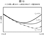
- FIG. 13 shows the hole density distribution between the emitter and collector during conduction.
- Vg -15V in the figure
- Vg 0V in the figure
- the absolute value of the gate negative voltage does not necessarily exceed the “threshold value (absolute value)” of the n-type collector layer 6, and the gate negative voltage Even if the absolute value of the voltage is lower than the “threshold value (absolute value)”, the potential of the channel with respect to the hole is lowered. Therefore, the hole passes through the channel path with the lowered potential and passes from the p + type cathode layer 13 to the n ⁇ It is injected into the type drift layer 1.
- FIG. 14 shows output characteristics when a positive voltage, zero volt, and negative voltage are applied to the gate electrode 8.
- a negative voltage is applied to the gate electrode 8 (as shown in FIG. 13)
- zero volt is applied to the gate electrode 8
- FIG. 15a and 15b show the gate drive sequence of this embodiment.
- FIG. 15a shows a sequence in which the collector current is the rated current
- FIG. 15b is a sequence in which the collector current is a small current.
- the gate on the collector side is set to a positive voltage, and charge injection from high charge injection mode (high speed) ) Switch to mode and reduce turn-off loss.
- the collector-side (rear surface) gate is held at a negative voltage (high charge injection mode), so that the collector-side hole density is kept high and vibration is suppressed.
- Example 7 of the present invention cross-sectional structure of a backside planar gate type IGBT semiconductor element
- FIG. 16 is a cross-sectional view of a seventh embodiment of the semiconductor element of the present invention.
- the present embodiment is different from the sixth embodiment in that the gate electrode 8 is not a trench type but a planar type. Similar to the sixth embodiment, this embodiment can also reduce loss and suppress vibration.
- the collector voltage and the collector current are oscillated by controlling the gate voltage on the collector side (back surface) according to the collector current. Can be suppressed.
- Example 8 (diode drive circuit) of the present invention will be described below.
- This embodiment is an embodiment of a circuit for driving the semiconductor elements (MOS control diodes) from the first embodiment to the fifth embodiment described above.
- FIG. 17 is a circuit diagram of the drive circuit of this embodiment.
- control circuit 20 the IGBT drive circuit 21, the drive circuit 22 of the semiconductor device of Embodiments 1 to 5, the upper arm IGBT 23, the lower arm IGBT 24, and the upper arm are applied to Embodiments 1 to 5.
- the circuit symbols of the semiconductor device 25 and the semiconductor device 26 represent that the resistance value of the diode is controlled by the gate electrode, which is devised for convenience by the inventors of the present application, and is not a general symbol.
- the recovery timing of the diode was detected from the operation of the inverter, and it was examined whether a positive voltage could be applied to the gate electrode immediately before recovery.
- the current detector 30 detects the current flowing through the diode. In addition to directly detecting the diode current, the current detector 30 can also indirectly detect the diode current by detecting the IGBT current. Further, the diode current can be estimated by detecting the motor current.
- the control circuit 20 determines which gate drive sequence to select between the rated current shown in FIG. 5a and the small current shown in FIG. 5b in accordance with the magnitude of the collector current detected by the current detector 30. decide.
- Example 9 of the present invention (a power converter to which the diode of the present invention is applied) will be described below.
- the feature of the present embodiment is that the diode described in the first to fifth embodiments is applied to the flyhole diode 600.
- the inverter device of FIG. 18 by applying the diodes of the first to fifth embodiments, the loss of the diode is reduced, and the inverter can be reduced in loss and size.
- Example 10 of the present invention (a power converter to which the IGBT of the present invention is applied) will be described below.
- the feature of the present embodiment is that the IGBT described in the sixth and seventh embodiments is applied to the IGBT 700.
- the IGBTs of the sixth embodiment and the seventh embodiment by applying the IGBTs of the sixth embodiment and the seventh embodiment, the loss of the diode is reduced, and the loss and the size of the inverter can be reduced.
- the configuration of the inverter device in FIG. 18 is an example, and the effect is the same even in an inverter device in which, for example, a series combination of switching elements and diodes connected in reverse parallel is coupled in the same number as the number of phases of AC output.
- an inverter that converts direct current to alternating current is shown.
- the present invention is not limited to this, and it will be apparent that the same effect can be obtained with a converter that converts alternating current to direct current.
- n + type emitter layer 600 ... flywheel diode, 700 ... IGBT, 800 ... gate circuit, 900 ... plus power terminal, 901 ... Negative power supply terminal, 910 ... U phase, 911 ... V phase, 912 ... W phase, 950 ... motor, 960: Power supply.
Landscapes
- Engineering & Computer Science (AREA)
- Power Engineering (AREA)
- Power Conversion In General (AREA)
- Inverter Devices (AREA)
- Electronic Switches (AREA)
- Thyristors (AREA)
Abstract
Description
3…p型チャネル層、
6…n型カソード層、
8…ゲート電極、
9…ゲート絶縁膜、
10…アノード電極、
11…カソード電極、
12…絶縁膜、
13…p+型カソード層、
20…制御回路、
21…IGBTの駆動回路、
22…ダイオードの駆動回路、
23…上アームIGBT、
24…下アームIGBT、
25…上アームのダイオード、
26…下アームのダイオード、
30…電流検出器、
40…エミッタ電極、
41…コレクタ電極、
42…p型チャネル層、
43…ゲート電極(IGBT)、
44…n+型エミッタ層、
600…フライホイールダイオード、
700…IGBT、
800…ゲート回路、
900…プラス側の電源端子、
901…マイナス側の電源端子、
910…U相、
911…V相、
912…W相、
950…モータ、
960…電源。
Claims (11)
- 第1導電型の第1半導体層(n-型ドリフト層)と、前記第1半導体層と隣接し、一方の主表面(アノード側)に露出する第2導電型の第2半導体層(p型アノード層)と、前記第1半導体層と隣接し、第1導電型で、他方の主表面(カソード側)に露出し、前記第1半導体層(n-型ドリフト層)より不純物濃度が高い第3半導体層(n型カソード層)と、前記他方の主表面(カソード側)に絶縁ゲートを備えた半導体素子の駆動装置であって、
アノード電流を検出する手段を備え、アノード電流が大きい時は、リカバリー直前に前記絶縁ゲートを正電圧から負電圧に切り替え、アノード電流が小さい時は、前記絶縁ゲートを正電圧に保持する
ことを特徴とする半導体素子の駆動装置。 - 第1導電型の第1半導体層(n-型ドリフト層)と、前記第1半導体層と隣接し、一方の主表面(アノード側)に露出する第2導電型の第2半導体層(p型アノード層)と、前記第1半導体層と隣接し、第1導電型で、他方の主表面(カソード側)に露出し、前記第1半導体層(n-型ドリフト層)より不純物濃度が高い第3半導体層(n型カソード層)と、前記第3半導体層(n型カソード層)を貫き、前記第1半導体層(n-型ドリフト層)に達する絶縁ゲートと、隣り合う前記絶縁ゲート間にあり、半導体層内で前記絶縁ゲートに接し、前記他方の主表面(カソード側)に露出する第2導電型の第4半導体層(p+型カソード層)と、前記第3半導体層と前記第4半導体層と電気的に接続される電極(カソード電極)を備えた半導体素子の駆動装置であって、
アノード電流を検出する手段を備え、アノード電流が大きい時は、リカバリー直前に前記絶縁ゲートを正電圧から負電圧に切り替え、アノード電流が小さい時は、前記絶縁ゲートを正電圧に保持する
ことを特徴とする半導体素子の駆動装置。 - 第1導電型の第1半導体層(n-型ドリフト層)と、前記第1半導体層と隣接し、一方の主表面(アノード側)に露出する第2導電型の第2半導体層(p型アノード層)と、前記第1半導体層と隣接し、第1導電型で、他方の主表面(カソード側)に露出し、前記第1半導体層(n-型ドリフト層)より不純物濃度が高い第3半導体層(n型カソード層)と、前記第3半導体層(n型カソード層)を貫き、前記第1半導体層(n-型ドリフト層)に達する絶縁ゲートと、前記第3半導体層と電気的に接続される電極(カソード電極)を備えた半導体素子の駆動装置であって、
アノード電流を検出する手段を備え、アノード電流が大きい時は、リカバリー直前に前記絶縁ゲートを正電圧から負電圧に切り替え、アノード電流が小さい時は、前記絶縁ゲートを正電圧に保持する
ことを特徴とする半導体素子の駆動装置。 - 第1導電型の第1半導体層(n-型ドリフト層)と、前記第1半導体層と隣接し、一方の主表面(アノード側)に露出する第2導電型の第2半導体層(p型アノード層)と、前記第1半導体層と隣接し、第1導電型で、他方の主表面(カソード側)に露出し、前記第1半導体層(n-型ドリフト層)より不純物濃度が高い第3半導体層(n型カソード層)と、前記他方の主表面(カソード側)に露出する第2導電型の第4半導体層(p+型カソード層)と、前記第1半導体層(n-型ドリフト層)と接する絶縁ゲートと、前記第3半導体層(n型カソード層)と接する前記絶縁ゲートと、前記第4半導体層(p+型カソード層)と接する前記絶縁ゲートと、前記第3半導体層と前記第4半導体層と電気的に接続される電極(カソード電極)を備えた半導体素子の駆動装置であって、
アノード電流を検出する手段を備え、アノード電流が大きい時は、リカバリー直前に前記絶縁ゲートを正電圧から負電圧に切り替え、アノード電流が小さい時は、前記絶縁ゲートを正電圧に保持する
ことを特徴とする半導体素子の駆動装置。 - 第1導電型の第1半導体層(n-型ドリフト層)と、前記第1半導体層と隣接し、一方の主表面(アノード側)に露出する第2導電型の第2半導体層(p型アノード層)と、前記第1半導体層と隣接し、第1導電型で、他方の主表面(カソード側)に露出し、前記第1半導体層(n-型ドリフト層)より不純物濃度が高い第3半導体層(n型カソード層)と、前記第1半導体層(n-型ドリフト層)と接する絶縁ゲートと、前記第3半導体層(n型カソード層)と接する前記絶縁ゲートと、前記第3半導体層と電気的に接続される電極(カソード電極)を備えた半導体素子の駆動装置であって、
アノード電流を検出する手段を備え、アノード電流が大きい時は、リカバリー直前に前記絶縁ゲートを正電圧から負電圧に切り替え、アノード電流が小さい時は、前記絶縁ゲートを正電圧に保持する
ことを特徴とする半導体素子の駆動装置。 - 請求項1乃至5のいずれかに記載の半導体素子の駆動装置において、
アノード電流の大小のしきい値を定格電流の1/2以下とする
ことを特徴とする半導体素子の駆動装置。 - 第1導電型の第1半導体層(n-型ドリフト層)と、前記第1半導体層と隣接し、一方の主表面に露出する第2導電型の第2半導体層(p型アノード層)と、前記第1半導体層と隣接し、第1導電型で、前記一方の主表面に露出し、前記第1半導体層(n-型ドリフト層)より不純物濃度が高い第3半導体層(n型カソード層)と、前記第3半導体層(n型カソード層)に隣接して絶縁ゲートを備えた半導体素子の駆動装置であって、
アノード電流を検出する手段を備え、アノード電流が大きい時は、リカバリー直前に前記絶縁ゲートを正電圧から負電圧に切り替え、アノード電流が小さい時は、前記絶縁ゲートを正電圧に保持する
ことを特徴とする半導体素子の駆動装置。 - 一対の直流端子と、前記一対の直流端子間に接続され、それぞれスイッチング素子と逆極性のダイオードの並列回路を2個直列接続した構成からなり、並列回路の相互接続点が交流端子に接続され、上記ダイオードに、請求項1乃至7のいずれかに記載の半導体素子が使用され、
前記2直列接続された第1スイッチング素子と第2スイッチング素子と、前記第1スイッチング素子と並列接続された第1ダイオードと、前記第2スイッチング素子と並列接続された第2ダイオードと、ダイオードのアノード電流を検出する電流検出器と、前記第1スイッチング素子と前記第2スイッチング素子と前記第1ダイオードと前記第2ダイオードの、それぞれのゲートを駆動する制御回路を備える
ことを特徴とする半導体素子の駆動装置。 - 第1導電型の第1半導体層(n-型ドリフト層)と、前記第1半導体層と隣接し、一方の主表面(エミッタ側)に露出する第2導電型の第2半導体層(p型チャネル層)と、前記一方の主表面(エミッタ側)に設けられ、主電流(コレクタ電流)をオン・オフする第1絶縁ゲートと、隣り合う前記第1絶縁ゲート間にあり、半導体層内で前記絶縁ゲートに接し、前記一方の主表面(エミッタ側)に露出する第1導電型の第5半導体層(n+型エミッタ層)と、前記第2半導体層と前記第5半導体層と電気的に接続される電極(エミッタ電極)と、前記第1半導体層と隣接し、第1導電型で他方の主表面(コレクタ側)に露出し、前記第1半導体層(n-型ドリフト層)より不純物濃度が高い第3半導体層(n型コレクタ層)と、前記他方の主表面(コレクタ側)に設けた第2の絶縁ゲートを備えた半導体素子の駆動装置であって、
コレクタ電流を検出する手段を備え、コレクタ電流が大きい時は、ターンオフ直前に前記第2絶縁ゲートを負電圧から正電圧に切り替え、コレクタ電流が小さい時は、前記第2絶縁ゲートを負電圧に保持する
ことを特徴とする半導体素子の駆動装置。 - 一対の直流端子と、交流の相数と同数の交流端子と、前記一対の直流端子との間に接続され、それぞれスイッチング素子と逆極性のダイオードの並列回路を2個直列接続した構成からなり、並列回路の相互接続点が異なる交流端子に接続された交流の相数と同数の電力変換単位とを具備し、かつ、前記ダイオードの駆動装置が、請求項1乃至8のいずれかに記載の半導体素子の駆動装置である
ことを特徴とする電力変換装置。 - 一対の直流端子と、交流の相数と同数の交流端子と、前記一対の直流端子との間に接続され、それぞれスイッチング素子と逆極性のダイオードの並列回路を2個直列接続した構成からなり、並列回路の相互接続点が異なる交流端子に接続された交流の相数と同数の電力変換単位とを具備し、かつ、前記スイッチング素子の駆動装置が、請求項9に記載の駆動装置である
ことを特徴とする電力変換装置。
Priority Applications (5)
| Application Number | Priority Date | Filing Date | Title |
|---|---|---|---|
| JP2015559682A JP6227677B2 (ja) | 2014-01-31 | 2014-01-31 | 半導体素子の駆動装置およびそれを用いた電力変換装置 |
| PCT/JP2014/052196 WO2015114787A1 (ja) | 2014-01-31 | 2014-01-31 | 半導体素子の駆動装置およびそれを用いた電力変換装置 |
| EP14881018.7A EP3101809A4 (en) | 2014-01-31 | 2014-01-31 | Semiconductor element drive apparatus and power conversion apparatus using same |
| US15/114,513 US20160343838A1 (en) | 2014-01-31 | 2014-01-31 | Semiconductor Element Drive Apparatus and Power Conversion Apparatus Using Same |
| CN201480074434.4A CN105940606B (zh) | 2014-01-31 | 2014-01-31 | 半导体元件的驱动装置及使用该驱动装置的电力变换装置 |
Applications Claiming Priority (1)
| Application Number | Priority Date | Filing Date | Title |
|---|---|---|---|
| PCT/JP2014/052196 WO2015114787A1 (ja) | 2014-01-31 | 2014-01-31 | 半導体素子の駆動装置およびそれを用いた電力変換装置 |
Publications (1)
| Publication Number | Publication Date |
|---|---|
| WO2015114787A1 true WO2015114787A1 (ja) | 2015-08-06 |
Family
ID=53756399
Family Applications (1)
| Application Number | Title | Priority Date | Filing Date |
|---|---|---|---|
| PCT/JP2014/052196 Ceased WO2015114787A1 (ja) | 2014-01-31 | 2014-01-31 | 半導体素子の駆動装置およびそれを用いた電力変換装置 |
Country Status (5)
| Country | Link |
|---|---|
| US (1) | US20160343838A1 (ja) |
| EP (1) | EP3101809A4 (ja) |
| JP (1) | JP6227677B2 (ja) |
| CN (1) | CN105940606B (ja) |
| WO (1) | WO2015114787A1 (ja) |
Cited By (6)
| Publication number | Priority date | Publication date | Assignee | Title |
|---|---|---|---|---|
| WO2018135224A1 (ja) * | 2017-01-18 | 2018-07-26 | 株式会社日立パワーデバイス | 半導体装置、及びそれを用いた電力変換装置 |
| JP2020053466A (ja) * | 2018-09-25 | 2020-04-02 | 三菱電機株式会社 | 半導体装置 |
| JP2020155581A (ja) * | 2019-03-20 | 2020-09-24 | 株式会社東芝 | 半導体装置 |
| JP2022527330A (ja) * | 2019-04-02 | 2022-06-01 | ヒタチ・エナジー・スウィツァーランド・アクチェンゲゼルシャフト | 逆回復が改善されたセグメント構造パワーダイオード |
| US11489066B2 (en) | 2020-11-06 | 2022-11-01 | Mitsubishi Electric Corporation | Semiconductor device |
| JP2024047735A (ja) * | 2022-09-27 | 2024-04-08 | 三菱電機株式会社 | 半導体装置および半導体装置の制御方法 |
Families Citing this family (6)
| Publication number | Priority date | Publication date | Assignee | Title |
|---|---|---|---|---|
| WO2019038755A1 (en) | 2017-08-24 | 2019-02-28 | Segasec Labs Ltd | DOMAIN USURPATION IDENTIFICATION SYSTEM |
| JP6820287B2 (ja) * | 2018-02-23 | 2021-01-27 | 株式会社 日立パワーデバイス | 半導体装置および電力変換装置 |
| JP6964538B2 (ja) * | 2018-02-28 | 2021-11-10 | 株式会社 日立パワーデバイス | 半導体装置および電力変換装置 |
| JP7315443B2 (ja) * | 2019-12-06 | 2023-07-26 | 株式会社日立製作所 | 半導体回路制御方法、及びそれを適用した電力変換器 |
| JP7722648B2 (ja) * | 2020-12-04 | 2025-08-13 | 国立大学法人 東京大学 | 半導体装置 |
| CN114203810A (zh) * | 2021-12-10 | 2022-03-18 | 电子科技大学 | 一种增加背面栅降低关断损耗的超高压igbt结构 |
Citations (7)
| Publication number | Priority date | Publication date | Assignee | Title |
|---|---|---|---|---|
| JPH06125256A (ja) * | 1992-05-01 | 1994-05-06 | Fuji Electric Co Ltd | ダブルゲート型半導体装置の制御装置 |
| JPH10163469A (ja) | 1996-11-29 | 1998-06-19 | Toshiba Corp | ダイオードおよびその駆動方法 |
| JP2001320049A (ja) | 2000-05-09 | 2001-11-16 | Fuji Electric Co Ltd | 半導体装置およびその製造方法 |
| JP2010123667A (ja) | 2008-11-18 | 2010-06-03 | Denso Corp | 半導体装置 |
| JP2010135676A (ja) * | 2008-12-08 | 2010-06-17 | Denso Corp | 絶縁ゲート型半導体装置の駆動回路およびそれに適した半導体装置 |
| JP2010251517A (ja) | 2009-04-15 | 2010-11-04 | Tokyo Electric Power Co Inc:The | パワー半導体素子 |
| JP2010283132A (ja) | 2009-06-04 | 2010-12-16 | Mitsubishi Electric Corp | 半導体装置 |
Family Cites Families (7)
| Publication number | Priority date | Publication date | Assignee | Title |
|---|---|---|---|---|
| JP5277579B2 (ja) * | 2007-07-25 | 2013-08-28 | 日産自動車株式会社 | 半導体装置 |
| JP5171776B2 (ja) * | 2009-09-30 | 2013-03-27 | 株式会社日立製作所 | 半導体装置、及びそれを用いた電力変換装置 |
| JP5229288B2 (ja) * | 2010-09-20 | 2013-07-03 | 株式会社デンソー | 半導体装置およびその制御方法 |
| DE102011079747A1 (de) * | 2010-07-27 | 2012-02-02 | Denso Corporation | Halbleitervorrichtung mit Schaltelement und Freilaufdiode, sowie Steuerverfahren hierfür |
| US9349847B2 (en) * | 2011-12-15 | 2016-05-24 | Hitachi, Ltd. | Semiconductor device and power converter |
| JP6015745B2 (ja) * | 2012-03-19 | 2016-10-26 | 富士電機株式会社 | 半導体装置の製造方法 |
| DE112013006639T5 (de) * | 2013-02-25 | 2015-10-29 | Hitachi, Ltd. | Halbleitervorrichtung, Treibervorrichtung für eine Halbleiterschaltung und Leistungswandlungsvorrichtung |
-
2014
- 2014-01-31 EP EP14881018.7A patent/EP3101809A4/en not_active Withdrawn
- 2014-01-31 WO PCT/JP2014/052196 patent/WO2015114787A1/ja not_active Ceased
- 2014-01-31 JP JP2015559682A patent/JP6227677B2/ja not_active Expired - Fee Related
- 2014-01-31 US US15/114,513 patent/US20160343838A1/en not_active Abandoned
- 2014-01-31 CN CN201480074434.4A patent/CN105940606B/zh not_active Expired - Fee Related
Patent Citations (7)
| Publication number | Priority date | Publication date | Assignee | Title |
|---|---|---|---|---|
| JPH06125256A (ja) * | 1992-05-01 | 1994-05-06 | Fuji Electric Co Ltd | ダブルゲート型半導体装置の制御装置 |
| JPH10163469A (ja) | 1996-11-29 | 1998-06-19 | Toshiba Corp | ダイオードおよびその駆動方法 |
| JP2001320049A (ja) | 2000-05-09 | 2001-11-16 | Fuji Electric Co Ltd | 半導体装置およびその製造方法 |
| JP2010123667A (ja) | 2008-11-18 | 2010-06-03 | Denso Corp | 半導体装置 |
| JP2010135676A (ja) * | 2008-12-08 | 2010-06-17 | Denso Corp | 絶縁ゲート型半導体装置の駆動回路およびそれに適した半導体装置 |
| JP2010251517A (ja) | 2009-04-15 | 2010-11-04 | Tokyo Electric Power Co Inc:The | パワー半導体素子 |
| JP2010283132A (ja) | 2009-06-04 | 2010-12-16 | Mitsubishi Electric Corp | 半導体装置 |
Non-Patent Citations (3)
| Title |
|---|
| K. NAKAMURA ET AL.: "Evaluation of Oscillatory Phenomena in Reverse Operation for High Voltage Diodes", PROC. IEEE ISPSD, 8 May 2009 (2009-05-08), pages 156 - 159 |
| M. RAHIMO ET AL.: "Freewheeling Diode Reverse-Recovery Failure Modes in IGBT Application", IEEE TRANS. INDUSTRY APPLICATION, vol. 37, no. 2, March 2001 (2001-03-01), pages 661 - 670, XP011022946 |
| See also references of EP3101809A4 |
Cited By (11)
| Publication number | Priority date | Publication date | Assignee | Title |
|---|---|---|---|---|
| WO2018135224A1 (ja) * | 2017-01-18 | 2018-07-26 | 株式会社日立パワーデバイス | 半導体装置、及びそれを用いた電力変換装置 |
| JP2018117044A (ja) * | 2017-01-18 | 2018-07-26 | 株式会社 日立パワーデバイス | 半導体装置、及びそれを用いた電力変換装置 |
| JP2020053466A (ja) * | 2018-09-25 | 2020-04-02 | 三菱電機株式会社 | 半導体装置 |
| JP7068981B2 (ja) | 2018-09-25 | 2022-05-17 | 三菱電機株式会社 | 半導体装置 |
| JP2020155581A (ja) * | 2019-03-20 | 2020-09-24 | 株式会社東芝 | 半導体装置 |
| JP7246983B2 (ja) | 2019-03-20 | 2023-03-28 | 株式会社東芝 | 半導体装置 |
| JP2022527330A (ja) * | 2019-04-02 | 2022-06-01 | ヒタチ・エナジー・スウィツァーランド・アクチェンゲゼルシャフト | 逆回復が改善されたセグメント構造パワーダイオード |
| JP7641909B2 (ja) | 2019-04-02 | 2025-03-07 | ヒタチ・エナジー・リミテッド | 逆回復が改善されたセグメント構造パワーダイオード |
| US11489066B2 (en) | 2020-11-06 | 2022-11-01 | Mitsubishi Electric Corporation | Semiconductor device |
| JP2024047735A (ja) * | 2022-09-27 | 2024-04-08 | 三菱電機株式会社 | 半導体装置および半導体装置の制御方法 |
| JP7814817B2 (ja) | 2022-09-27 | 2026-02-17 | 三菱電機株式会社 | 半導体装置の制御方法 |
Also Published As
| Publication number | Publication date |
|---|---|
| US20160343838A1 (en) | 2016-11-24 |
| EP3101809A4 (en) | 2017-08-23 |
| EP3101809A1 (en) | 2016-12-07 |
| JP6227677B2 (ja) | 2017-11-08 |
| CN105940606A (zh) | 2016-09-14 |
| JPWO2015114787A1 (ja) | 2017-03-23 |
| CN105940606B (zh) | 2018-10-12 |
Similar Documents
| Publication | Publication Date | Title |
|---|---|---|
| JP6227677B2 (ja) | 半導体素子の駆動装置およびそれを用いた電力変換装置 | |
| JP4644730B2 (ja) | 半導体装置及びそれを用いた電力変換装置 | |
| CN111418071B (zh) | 半导体装置以及功率变换装置 | |
| US9595602B2 (en) | Switching device for power conversion and power conversion device | |
| CN110678988B (zh) | 半导体装置 | |
| JP5171776B2 (ja) | 半導体装置、及びそれを用いた電力変換装置 | |
| JP6709062B2 (ja) | 半導体装置、その製造方法、及びそれを用いた電力変換装置 | |
| CN111788695B (zh) | 半导体装置以及电力变换装置 | |
| JP5875680B2 (ja) | 絶縁ゲート型バイポーラトランジスタ | |
| CN104576718A (zh) | 具有续流SiC二极管的RC-IGBT | |
| JP2014112578A (ja) | 半導体装置およびそれを用いた電力変換装置 | |
| US20160013299A1 (en) | Semiconductor device, drive device for semiconductor circuit, and power conversion device | |
| US20150162429A1 (en) | Semiconductor Device and Power Conversion Device Using the Same | |
| US20160013300A1 (en) | Semiconductor device, drive device for semiconductor circuit, and power conversion device | |
| EP4071813B1 (en) | Semiconductor-circuit control method and electric power converter to which the same is applied | |
| US9306047B2 (en) | Semiconductor device and electric power converter in which same is used | |
| JP5017850B2 (ja) | 電力用半導体装置およびそれを用いた電力変換装置 | |
| Eckel et al. | Turn-off behaviour of high voltage NPT-and FS-IGBT | |
| JP2015204723A (ja) | 半導体装置及びそれを用いた電力変換装置 | |
| WO2014086015A1 (zh) | 一种ti-igbt及其形成方法 | |
| CN106783991B (zh) | 一种自驱动阳极辅助栅绝缘栅双极型晶体管 | |
| WO2014128943A1 (ja) | 半導体装置およびそれを用いた電力変換装置 | |
| JPWO2013111294A1 (ja) | 半導体装置およびそれを用いた電力変換装置 |
Legal Events
| Date | Code | Title | Description |
|---|---|---|---|
| 121 | Ep: the epo has been informed by wipo that ep was designated in this application |
Ref document number: 14881018 Country of ref document: EP Kind code of ref document: A1 |
|
| ENP | Entry into the national phase |
Ref document number: 2015559682 Country of ref document: JP Kind code of ref document: A |
|
| WWE | Wipo information: entry into national phase |
Ref document number: 15114513 Country of ref document: US |
|
| REEP | Request for entry into the european phase |
Ref document number: 2014881018 Country of ref document: EP |
|
| WWE | Wipo information: entry into national phase |
Ref document number: 2014881018 Country of ref document: EP |
|
| NENP | Non-entry into the national phase |
Ref country code: DE |