WO2015118982A1 - 電子部品モジュール、および電子部品モジュールの製造方法 - Google Patents
電子部品モジュール、および電子部品モジュールの製造方法 Download PDFInfo
- Publication number
- WO2015118982A1 WO2015118982A1 PCT/JP2015/052018 JP2015052018W WO2015118982A1 WO 2015118982 A1 WO2015118982 A1 WO 2015118982A1 JP 2015052018 W JP2015052018 W JP 2015052018W WO 2015118982 A1 WO2015118982 A1 WO 2015118982A1
- Authority
- WO
- WIPO (PCT)
- Prior art keywords
- electronic component
- copper
- component module
- copper particles
- particles
- Prior art date
- Legal status (The legal status is an assumption and is not a legal conclusion. Google has not performed a legal analysis and makes no representation as to the accuracy of the status listed.)
- Ceased
Links
Images


Classifications
-
- H—ELECTRICITY
- H01—ELECTRIC ELEMENTS
- H01B—CABLES; CONDUCTORS; INSULATORS; SELECTION OF MATERIALS FOR THEIR CONDUCTIVE, INSULATING OR DIELECTRIC PROPERTIES
- H01B1/00—Conductors or conductive bodies characterised by the conductive materials; Selection of materials as conductors
- H01B1/20—Conductive material dispersed in non-conductive organic material
- H01B1/22—Conductive material dispersed in non-conductive organic material the conductive material comprising metals or alloys
-
- B—PERFORMING OPERATIONS; TRANSPORTING
- B22—CASTING; POWDER METALLURGY
- B22F—WORKING METALLIC POWDER; MANUFACTURE OF ARTICLES FROM METALLIC POWDER; MAKING METALLIC POWDER; APPARATUS OR DEVICES SPECIALLY ADAPTED FOR METALLIC POWDER
- B22F1/00—Metallic powder; Treatment of metallic powder, e.g. to facilitate working or to improve properties
- B22F1/10—Metallic powder containing lubricating or binding agents; Metallic powder containing organic material
-
- B—PERFORMING OPERATIONS; TRANSPORTING
- B22—CASTING; POWDER METALLURGY
- B22F—WORKING METALLIC POWDER; MANUFACTURE OF ARTICLES FROM METALLIC POWDER; MAKING METALLIC POWDER; APPARATUS OR DEVICES SPECIALLY ADAPTED FOR METALLIC POWDER
- B22F7/00—Manufacture of composite layers, workpieces, or articles, comprising metallic powder, by sintering the powder, with or without compacting wherein at least one part is obtained by sintering or compression
- B22F7/06—Manufacture of composite layers, workpieces, or articles, comprising metallic powder, by sintering the powder, with or without compacting wherein at least one part is obtained by sintering or compression of composite workpieces or articles from parts, e.g. to form tipped tools
- B22F7/062—Manufacture of composite layers, workpieces, or articles, comprising metallic powder, by sintering the powder, with or without compacting wherein at least one part is obtained by sintering or compression of composite workpieces or articles from parts, e.g. to form tipped tools involving the connection or repairing of preformed parts
- B22F7/064—Manufacture of composite layers, workpieces, or articles, comprising metallic powder, by sintering the powder, with or without compacting wherein at least one part is obtained by sintering or compression of composite workpieces or articles from parts, e.g. to form tipped tools involving the connection or repairing of preformed parts using an intermediate powder layer
-
- H—ELECTRICITY
- H05—ELECTRIC TECHNIQUES NOT OTHERWISE PROVIDED FOR
- H05K—PRINTED CIRCUITS; CASINGS OR CONSTRUCTIONAL DETAILS OF ELECTRIC APPARATUS; MANUFACTURE OF ASSEMBLAGES OF ELECTRICAL COMPONENTS
- H05K1/00—Printed circuits
- H05K1/02—Details
- H05K1/09—Use of materials for the conductive, e.g. metallic pattern
- H05K1/092—Dispersed materials, e.g. conductive pastes or inks
- H05K1/097—Inks comprising nanoparticles and specially adapted for being sintered at low temperature
-
- H—ELECTRICITY
- H05—ELECTRIC TECHNIQUES NOT OTHERWISE PROVIDED FOR
- H05K—PRINTED CIRCUITS; CASINGS OR CONSTRUCTIONAL DETAILS OF ELECTRIC APPARATUS; MANUFACTURE OF ASSEMBLAGES OF ELECTRICAL COMPONENTS
- H05K1/00—Printed circuits
- H05K1/18—Printed circuits structurally associated with non-printed electric components
- H05K1/181—Printed circuits structurally associated with non-printed electric components associated with surface mounted components
-
- H—ELECTRICITY
- H05—ELECTRIC TECHNIQUES NOT OTHERWISE PROVIDED FOR
- H05K—PRINTED CIRCUITS; CASINGS OR CONSTRUCTIONAL DETAILS OF ELECTRIC APPARATUS; MANUFACTURE OF ASSEMBLAGES OF ELECTRICAL COMPONENTS
- H05K3/00—Apparatus or processes for manufacturing printed circuits
- H05K3/30—Assembling printed circuits with electric components, e.g. with resistors
- H05K3/32—Assembling printed circuits with electric components, e.g. with resistors electrically connecting electric components or wires to printed circuits
-
- H—ELECTRICITY
- H10—SEMICONDUCTOR DEVICES; ELECTRIC SOLID-STATE DEVICES NOT OTHERWISE PROVIDED FOR
- H10W—GENERIC PACKAGES, INTERCONNECTIONS, CONNECTORS OR OTHER CONSTRUCTIONAL DETAILS OF DEVICES COVERED BY CLASS H10
- H10W72/00—Interconnections or connectors in packages
- H10W72/20—Bump connectors, e.g. solder bumps or copper pillars; Dummy bumps; Thermal bumps
-
- B—PERFORMING OPERATIONS; TRANSPORTING
- B23—MACHINE TOOLS; METAL-WORKING NOT OTHERWISE PROVIDED FOR
- B23K—SOLDERING OR UNSOLDERING; WELDING; CLADDING OR PLATING BY SOLDERING OR WELDING; CUTTING BY APPLYING HEAT LOCALLY, e.g. FLAME CUTTING; WORKING BY LASER BEAM
- B23K35/00—Rods, electrodes, materials, or media, for use in soldering, welding, or cutting
- B23K35/02—Rods, electrodes, materials, or media, for use in soldering, welding, or cutting characterised by mechanical features, e.g. shape
- B23K35/0222—Rods, electrodes, materials, or media, for use in soldering, welding, or cutting characterised by mechanical features, e.g. shape for use in soldering or brazing
- B23K35/0244—Powders, particles or spheres; Preforms made therefrom
- B23K35/025—Pastes, creams or slurries
-
- B—PERFORMING OPERATIONS; TRANSPORTING
- B23—MACHINE TOOLS; METAL-WORKING NOT OTHERWISE PROVIDED FOR
- B23K—SOLDERING OR UNSOLDERING; WELDING; CLADDING OR PLATING BY SOLDERING OR WELDING; CUTTING BY APPLYING HEAT LOCALLY, e.g. FLAME CUTTING; WORKING BY LASER BEAM
- B23K35/00—Rods, electrodes, materials, or media, for use in soldering, welding, or cutting
- B23K35/22—Rods, electrodes, materials, or media, for use in soldering, welding, or cutting characterised by the composition or nature of the material
- B23K35/24—Selection of soldering or welding materials proper
- B23K35/30—Selection of soldering or welding materials proper with the principal constituent melting at less than 1550°C
- B23K35/302—Cu as the principal constituent
-
- H—ELECTRICITY
- H05—ELECTRIC TECHNIQUES NOT OTHERWISE PROVIDED FOR
- H05K—PRINTED CIRCUITS; CASINGS OR CONSTRUCTIONAL DETAILS OF ELECTRIC APPARATUS; MANUFACTURE OF ASSEMBLAGES OF ELECTRICAL COMPONENTS
- H05K2201/00—Indexing scheme relating to printed circuits covered by H05K1/00
- H05K2201/02—Fillers; Particles; Fibers; Reinforcement materials
- H05K2201/0203—Fillers and particles
- H05K2201/0242—Shape of an individual particle
- H05K2201/0257—Nanoparticles
-
- H—ELECTRICITY
- H05—ELECTRIC TECHNIQUES NOT OTHERWISE PROVIDED FOR
- H05K—PRINTED CIRCUITS; CASINGS OR CONSTRUCTIONAL DETAILS OF ELECTRIC APPARATUS; MANUFACTURE OF ASSEMBLAGES OF ELECTRICAL COMPONENTS
- H05K2201/00—Indexing scheme relating to printed circuits covered by H05K1/00
- H05K2201/10—Details of components or other objects attached to or integrated in a printed circuit board
- H05K2201/10007—Types of components
- H05K2201/10015—Non-printed capacitor
-
- H—ELECTRICITY
- H05—ELECTRIC TECHNIQUES NOT OTHERWISE PROVIDED FOR
- H05K—PRINTED CIRCUITS; CASINGS OR CONSTRUCTIONAL DETAILS OF ELECTRIC APPARATUS; MANUFACTURE OF ASSEMBLAGES OF ELECTRICAL COMPONENTS
- H05K2203/00—Indexing scheme relating to apparatus or processes for manufacturing printed circuits covered by H05K3/00
- H05K2203/11—Treatments characterised by their effect, e.g. heating, cooling, roughening
- H05K2203/1131—Sintering, i.e. fusing of metal particles to achieve or improve electrical conductivity
-
- H—ELECTRICITY
- H10—SEMICONDUCTOR DEVICES; ELECTRIC SOLID-STATE DEVICES NOT OTHERWISE PROVIDED FOR
- H10W—GENERIC PACKAGES, INTERCONNECTIONS, CONNECTORS OR OTHER CONSTRUCTIONAL DETAILS OF DEVICES COVERED BY CLASS H10
- H10W72/00—Interconnections or connectors in packages
- H10W72/01—Manufacture or treatment
- H10W72/013—Manufacture or treatment of die-attach connectors
- H10W72/01321—Manufacture or treatment of die-attach connectors using local deposition
- H10W72/01323—Manufacture or treatment of die-attach connectors using local deposition in liquid form, e.g. by dispensing droplets or by screen printing
-
- H—ELECTRICITY
- H10—SEMICONDUCTOR DEVICES; ELECTRIC SOLID-STATE DEVICES NOT OTHERWISE PROVIDED FOR
- H10W—GENERIC PACKAGES, INTERCONNECTIONS, CONNECTORS OR OTHER CONSTRUCTIONAL DETAILS OF DEVICES COVERED BY CLASS H10
- H10W72/00—Interconnections or connectors in packages
- H10W72/01—Manufacture or treatment
- H10W72/016—Manufacture or treatment of strap connectors
-
- H—ELECTRICITY
- H10—SEMICONDUCTOR DEVICES; ELECTRIC SOLID-STATE DEVICES NOT OTHERWISE PROVIDED FOR
- H10W—GENERIC PACKAGES, INTERCONNECTIONS, CONNECTORS OR OTHER CONSTRUCTIONAL DETAILS OF DEVICES COVERED BY CLASS H10
- H10W72/00—Interconnections or connectors in packages
- H10W72/071—Connecting or disconnecting
- H10W72/072—Connecting or disconnecting of bump connectors
- H10W72/07251—Connecting or disconnecting of bump connectors characterised by changes in properties of the bump connectors during connecting
- H10W72/07255—Connecting or disconnecting of bump connectors characterised by changes in properties of the bump connectors during connecting changes in materials
-
- H—ELECTRICITY
- H10—SEMICONDUCTOR DEVICES; ELECTRIC SOLID-STATE DEVICES NOT OTHERWISE PROVIDED FOR
- H10W—GENERIC PACKAGES, INTERCONNECTIONS, CONNECTORS OR OTHER CONSTRUCTIONAL DETAILS OF DEVICES COVERED BY CLASS H10
- H10W72/00—Interconnections or connectors in packages
- H10W72/071—Connecting or disconnecting
- H10W72/073—Connecting or disconnecting of die-attach connectors
- H10W72/07331—Connecting techniques
-
- H—ELECTRICITY
- H10—SEMICONDUCTOR DEVICES; ELECTRIC SOLID-STATE DEVICES NOT OTHERWISE PROVIDED FOR
- H10W—GENERIC PACKAGES, INTERCONNECTIONS, CONNECTORS OR OTHER CONSTRUCTIONAL DETAILS OF DEVICES COVERED BY CLASS H10
- H10W72/00—Interconnections or connectors in packages
- H10W72/071—Connecting or disconnecting
- H10W72/073—Connecting or disconnecting of die-attach connectors
- H10W72/07341—Controlling the bonding environment, e.g. atmosphere composition or temperature
-
- H—ELECTRICITY
- H10—SEMICONDUCTOR DEVICES; ELECTRIC SOLID-STATE DEVICES NOT OTHERWISE PROVIDED FOR
- H10W—GENERIC PACKAGES, INTERCONNECTIONS, CONNECTORS OR OTHER CONSTRUCTIONAL DETAILS OF DEVICES COVERED BY CLASS H10
- H10W72/00—Interconnections or connectors in packages
- H10W72/20—Bump connectors, e.g. solder bumps or copper pillars; Dummy bumps; Thermal bumps
- H10W72/221—Structures or relative sizes
- H10W72/225—Bumps having a filler embedded in a matrix
-
- H—ELECTRICITY
- H10—SEMICONDUCTOR DEVICES; ELECTRIC SOLID-STATE DEVICES NOT OTHERWISE PROVIDED FOR
- H10W—GENERIC PACKAGES, INTERCONNECTIONS, CONNECTORS OR OTHER CONSTRUCTIONAL DETAILS OF DEVICES COVERED BY CLASS H10
- H10W72/00—Interconnections or connectors in packages
- H10W72/20—Bump connectors, e.g. solder bumps or copper pillars; Dummy bumps; Thermal bumps
- H10W72/241—Dispositions, e.g. layouts
-
- H—ELECTRICITY
- H10—SEMICONDUCTOR DEVICES; ELECTRIC SOLID-STATE DEVICES NOT OTHERWISE PROVIDED FOR
- H10W—GENERIC PACKAGES, INTERCONNECTIONS, CONNECTORS OR OTHER CONSTRUCTIONAL DETAILS OF DEVICES COVERED BY CLASS H10
- H10W72/00—Interconnections or connectors in packages
- H10W72/20—Bump connectors, e.g. solder bumps or copper pillars; Dummy bumps; Thermal bumps
- H10W72/251—Materials
- H10W72/252—Materials comprising solid metals or solid metalloids, e.g. PbSn, Ag or Cu
- H10W72/2528—Intermetallic compounds
-
- H—ELECTRICITY
- H10—SEMICONDUCTOR DEVICES; ELECTRIC SOLID-STATE DEVICES NOT OTHERWISE PROVIDED FOR
- H10W—GENERIC PACKAGES, INTERCONNECTIONS, CONNECTORS OR OTHER CONSTRUCTIONAL DETAILS OF DEVICES COVERED BY CLASS H10
- H10W72/00—Interconnections or connectors in packages
- H10W72/20—Bump connectors, e.g. solder bumps or copper pillars; Dummy bumps; Thermal bumps
- H10W72/251—Materials
- H10W72/253—Materials not comprising solid metals or solid metalloids, e.g. polymers or ceramics
-
- H—ELECTRICITY
- H10—SEMICONDUCTOR DEVICES; ELECTRIC SOLID-STATE DEVICES NOT OTHERWISE PROVIDED FOR
- H10W—GENERIC PACKAGES, INTERCONNECTIONS, CONNECTORS OR OTHER CONSTRUCTIONAL DETAILS OF DEVICES COVERED BY CLASS H10
- H10W72/00—Interconnections or connectors in packages
- H10W72/30—Die-attach connectors
- H10W72/321—Structures or relative sizes of die-attach connectors
- H10W72/325—Die-attach connectors having a filler embedded in a matrix
-
- H—ELECTRICITY
- H10—SEMICONDUCTOR DEVICES; ELECTRIC SOLID-STATE DEVICES NOT OTHERWISE PROVIDED FOR
- H10W—GENERIC PACKAGES, INTERCONNECTIONS, CONNECTORS OR OTHER CONSTRUCTIONAL DETAILS OF DEVICES COVERED BY CLASS H10
- H10W72/00—Interconnections or connectors in packages
- H10W72/30—Die-attach connectors
- H10W72/351—Materials of die-attach connectors
- H10W72/352—Materials of die-attach connectors comprising metals or metalloids, e.g. solders
-
- H—ELECTRICITY
- H10—SEMICONDUCTOR DEVICES; ELECTRIC SOLID-STATE DEVICES NOT OTHERWISE PROVIDED FOR
- H10W—GENERIC PACKAGES, INTERCONNECTIONS, CONNECTORS OR OTHER CONSTRUCTIONAL DETAILS OF DEVICES COVERED BY CLASS H10
- H10W72/00—Interconnections or connectors in packages
- H10W72/30—Die-attach connectors
- H10W72/351—Materials of die-attach connectors
- H10W72/353—Materials of die-attach connectors not comprising solid metals or solid metalloids, e.g. ceramics
- H10W72/354—Materials of die-attach connectors not comprising solid metals or solid metalloids, e.g. ceramics comprising polymers
-
- H—ELECTRICITY
- H10—SEMICONDUCTOR DEVICES; ELECTRIC SOLID-STATE DEVICES NOT OTHERWISE PROVIDED FOR
- H10W—GENERIC PACKAGES, INTERCONNECTIONS, CONNECTORS OR OTHER CONSTRUCTIONAL DETAILS OF DEVICES COVERED BY CLASS H10
- H10W74/00—Encapsulations, e.g. protective coatings
- H10W74/10—Encapsulations, e.g. protective coatings characterised by their shape or disposition
- H10W74/111—Encapsulations, e.g. protective coatings characterised by their shape or disposition the semiconductor body being completely enclosed
- H10W74/114—Encapsulations, e.g. protective coatings characterised by their shape or disposition the semiconductor body being completely enclosed by a substrate and the encapsulations
-
- H—ELECTRICITY
- H10—SEMICONDUCTOR DEVICES; ELECTRIC SOLID-STATE DEVICES NOT OTHERWISE PROVIDED FOR
- H10W—GENERIC PACKAGES, INTERCONNECTIONS, CONNECTORS OR OTHER CONSTRUCTIONAL DETAILS OF DEVICES COVERED BY CLASS H10
- H10W90/00—Package configurations
- H10W90/701—Package configurations characterised by the relative positions of pads or connectors relative to package parts
- H10W90/721—Package configurations characterised by the relative positions of pads or connectors relative to package parts of bump connectors
- H10W90/724—Package configurations characterised by the relative positions of pads or connectors relative to package parts of bump connectors between a chip and a stacked insulating package substrate, interposer or RDL
Definitions
- the present invention relates to an electronic component module manufactured using a copper particle paste and a method for manufacturing the electronic component module.
- Patent Document 1 discloses a liquid or paste containing copper nanoparticles having a particle size of 1000 nm or less, and the particle size peak of the particle size distribution based on the number of copper nanoparticles is 1 One or more in each of a section of ⁇ 35 nm and a section having a particle size larger than 35 nm and smaller than or equal to 1000 nm, and the copper nanoparticles include primary particles and secondary particles that are a fusion of primary particles. Materials have been proposed.
- Patent Document 1 discloses that the above-described sinterable bonding material contains a dispersant (dispersion stabilizer), and an atmosphere of hydrogen, formic acid, or ethanol is disclosed as a reducing atmosphere in the firing step. Has been.
- Patent Document 1 discloses that when an electronic component is bonded using the sinterable bonding material, a sintering heat treatment is performed while applying pressure in a direction in which the electronic component is bonded.
- the atmosphere of hydrogen, formic acid, or ethanol is used as a firing atmosphere
- a reducing atmosphere gas is not supplied to the inner region of the joint, and the inner region is desirably reduced
- firing is likely to proceed in the vicinity of the outer periphery of the joint portion in contact with the reducing atmosphere, and firing is difficult to proceed in the inner region, so that an unsintered region is formed in the inner region, resulting in a decrease in joint strength.
- the present invention solves the above-mentioned problem, and is excellent in stability (oxidation resistance) of copper particles that are conductive components, and it is difficult to form voids and can form a bonding portion with high bonding reliability.
- the electronic component module of the present invention is An external component included in the electronic component is an electronic component module having a structure in which the external terminal is electrically and mechanically connected to a connection target via a bonding material,
- the bonding material is
- the particle size distribution has a particle size peak in the range of 0.1 to 5.0 ⁇ m, an average crystallite size before sintering in the range of 30 to 100 nm, and a dispersing agent that suppresses aggregation on the particle surface.
- the bonding material is preferably a copper sintered body having an average crystallite diameter of the sintered copper particles in the range of 60 to 150 nm.
- a stable copper sintered body is formed by adjusting the average crystallite diameter after sintering to 60 to 150 nm.
- the said organic compound is an organic compound which has a hydroxyl group. Removing the oxide film formed on the surface of the copper particles in the firing step by using an organic compound having a hydroxy group as an organic compound having a reducing action at the firing temperature for sintering the copper particles; In the firing step, copper can be surely sintered without being oxidized, and the present invention can be made more effective.
- the organic compound preferably contains at least one selected from the group consisting of triethanolamine, glycerin, ethylene glycol, triethylene glycol, diethylene glycol, and dipropylene glycol.
- connection target is a mounting electrode disposed on a circuit board.
- a structure in which a surface mount type electronic component such as an IC chip or a multilayer ceramic capacitor is mounted on the circuit board is provided. It is possible to reliably manufacture a highly reliable electronic component module.
- connection object is a metal terminal attached to the external terminal.
- the manufacturing method of the electronic component module of the present invention includes:
- An external terminal included in an electronic component is a method for manufacturing an electronic component module having a structure in which an external terminal is electrically and mechanically connected to a connection target via a bonding material,
- the external terminal of the electronic component has a particle size distribution with a particle size peak in the range of 0.1 to 5.0 ⁇ m, an average crystallite size before sintering in the range of 30 to 100 nm, and agglomeration.
- a copper sintered body having an average crystallite diameter of the copper particles of 60 to 150 nm is formed, and the external terminals of the electronic component and A step of joining the connection object via the copper sintered body.
- the electronic component is placed on the joining target so that the external terminal of the electronic component faces the connection target via the copper particle paste.
- the heat treatment is preferably performed in an inert atmosphere.
- the copper particles constituting the copper particle paste can be more reliably sintered, and the present invention can be made more effective.
- the copper particles used as the copper particles constituting the above copper particle paste and having a particle size distribution having a particle size peak in the range of 0.1 to 5.0 ⁇ m are not excessively fine and are not easily oxidized.
- the average crystallite diameter is as small as 30 to 100 nm and can be sintered at a low temperature of 300 ° C. or lower. After sintering, the average crystallite diameter is 60 It is a copper particle that becomes a copper sintered body of about 150 nm and becomes a stable bonding material.
- the copper particles do not have a dispersant for suppressing aggregation on the surface, it is possible to obtain a sintered body in which the density of the copper sintered body obtained by sintering is high and the proportion of voids is small. it can.
- the average crystallite size of the copper particles is 30 to 100 nm. By making it in this range, low temperature sintering at 300 ° C. or lower is enabled.
- the above copper particle paste contains an organic compound (for example, a solvent) that exhibits a reducing action at a firing temperature for sintering the copper particles. Since the copper oxide on the surface of the copper particles, which becomes an inhibiting factor, is reduced, it is not particularly necessary to fire in a reducing atmosphere, and sintering in an inert atmosphere becomes possible. When firing in a reducing atmosphere using a reducing gas, when the above copper particle paste is used as a bonding material, sintering progresses on the surface and the peripheral portion of the bonded portion, and is fired inside the bonded portion. Although there is a problem that the result tends to be insufficient, as described above, the inclusion of an organic compound (for example, a solvent) that exhibits a reducing action eliminates the need for firing in a reducing atmosphere, thus eliminating this problem. can do.
- an organic compound for example, a solvent
- 1A to 1D are diagrams schematically showing a process of sintering copper particles.
- the copper particles 10 used in the copper particle paste have a large grain boundary energy, with the average size (average crystallite diameter) of the crystallites 11 being as small as 30 to 100 nm. .
- the surface of the copper particles 10 is covered with an oxide film (copper oxide) 12 at room temperature.
- this copper particle paste (copper particle) 1 is heated to a reflow temperature (for example, 230 ° C.), as shown in FIG. 1B, the firing temperature for sintering the copper particles present around the copper particles 10
- the organic compound (for example, a solvent) 13 having a reducing action acts as a reducing agent, and the oxide film (copper oxide) 12 on the surface of the copper particles 10 is reduced.
- the oxide film (copper oxide) 12 on the surface of the copper particle 10 is reduced, the copper particle 10 having a small average crystallite diameter and a large grain boundary energy can be obtained even at a temperature as low as the reflow temperature.
- the neck grows and coalesces as shown in FIG. 1C to increase the crystallite diameter.
- the copper particles 10 themselves become large and the average crystallite diameter becomes as large as 60 to 150 nm, and a stable copper sintered body is formed.
- the copper particles constituting the copper particle paste can be efficiently sintered even at a low temperature by such a mechanism.
- the electronic component module of the present invention has a structure in which the external terminals provided in the electronic component are electrically and mechanically connected to the connection target via the bonding material formed by baking the copper particle paste. It has high reliability because the external terminals of the electronic component and the connection target are securely joined via a joint made of a copper sintered body with a high density and a small proportion of voids. An electronic component module can be reliably provided.
- the method for manufacturing an electronic component module according to the present invention includes a heat treatment in a state where the electronic component and the bonding target are positioned so that the external terminal of the electronic component faces the connection target via the copper particle paste.
- the copper particles contained in the copper particle paste are sintered, and the external terminals of the electronic component and the connection target are joined by a copper sintered body having an average crystallite diameter of 60 to 150 nm. It is possible to reliably join the external terminals of the component and the connection target through a joint made of a copper sintered body with a high density and a small proportion of voids, and a highly reliable electronic component module can be efficiently used. Can be manufactured well.
- the external terminals included in the electronic component are electrically and mechanically connected to the connection target via a bonding material formed by sintering a copper particle paste.
- the electronic component module having the above structure.
- the copper particle has a particle size distribution having a particle size peak in the range of 0.1 to 5.0 ⁇ m and an average crystallite size before sintering of 30 to 100 nm. Copper particles in the range were prepared.
- triethanolamine which is liquid at room temperature, was prepared as an organic compound that exhibits a reducing action at the firing temperature when sintering the copper particles.
- copper particles and triethanolamine were blended at a ratio of 87:13 by weight and kneaded to prepare a copper particle paste.
- the particle size peak of the particle size distribution of the copper particles was determined by the following method. First, copper particles were observed using a scanning electron microscope, and the horizontal ferret diameter was measured for 200 particles in the field of view. And the measured value obtained was converted into a sphere, the volume average particle size was calculated, and the particle size peak was obtained from the result.
- the average crystallite size before sintering was determined by the following method. First, X-ray diffraction measurement was performed on the copper particles, and three peaks ⁇ 111>, ⁇ 200>, and ⁇ 311> were obtained. Then, using the obtained three peaks, the crystallite diameter was calculated by the Rietveld method, and the average value was taken as the average crystallite diameter.
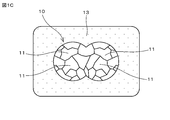
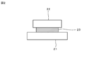
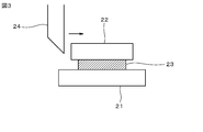
- a first oxygen-free copper sample piece 21 having a plane dimension of 5 mm in length and width and a thickness of 1 mm
- a second oxygen-free copper sample having a plane dimension of 3 mm in length and breadth and a thickness of 1 mm.
- the pieces 22 were joined via a copper sintered body 23 formed by firing the copper particle paste produced as described above.
- a through hole (here, a plane having a diameter of 2000 ⁇ m) through which the copper particle paste passes is used.
- the copper particle paste was printed on the first oxygen-free copper sample piece 21 so that the coating thickness was 40 ⁇ m.
- the second oxygen-free copper sample piece 22 is placed on the copper particle paste printed on the first oxygen-free copper sample piece 21, no particular stress is applied, and the baking temperature is 230 ° C. and the baking time is: As shown in FIG. 2, the first oxygen-free copper sample piece 21 and the second oxygen-free copper sample piece 22 are bonded to a bonding material (copper particle paste) by baking under a condition of baking atmosphere: nitrogen for 60 minutes. The sintered copper sintered body) 23 was joined.
- the bonding strength between the first oxygen-free copper sample piece 21 and the second oxygen-free copper sample piece 22 was measured.
- the measurement of the joint strength was performed by measuring the shear strength using a universal bond tester Dage 4000 manufactured by Dage.
- the lower first oxygen-free copper sample piece 21 is fixed with a fixing jig, a shear tool 24 having a tool width of 4 mm is used, a shear rate of 50 ⁇ m / s, and no The distance from the surface of the oxygen copper sample piece 21 to the tip of the tool was 50 ⁇ m and shared. Then, the fracture surface was photographed, and the bonding area was measured by image processing. *
- the average crystallite diameter before firing is obtained by applying copper particle paste to a glass plate with ink and performing the above-described method, that is, X-ray diffraction measurement.
- the crystallite diameter was calculated from the three peaks ⁇ 111>, ⁇ 200>, and ⁇ 311> by the Rietveld method, and the average value was obtained.
- the average crystallite diameter after firing is the peak ⁇ 111> obtained by extracting the sintered body after sharing using tweezers and placing it on a glass plate and performing the above-described method, that is, X-ray diffraction measurement.
- ⁇ 200>, ⁇ 311> The crystallite diameter was calculated by the Rietveld method from the three peaks, and the average value was obtained.
- the copper particle paste is printed on the first oxygen-free copper sample piece 21 so that the coating thickness is 40 ⁇ m. Then, firing was performed under the conditions of: temperature: 230 ° C., firing time: 60 min, firing atmosphere: nitrogen, and the crystallite diameter before and after firing was examined.
- the mechanism described above with reference to FIGS. 1A to 1D enables sintering at a low temperature. As a result, it is possible to form a bonding material made of a copper sintered body having a high density and a small proportion of voids without requiring firing at a high temperature.
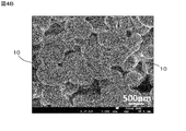
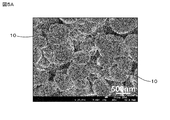
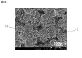
- FIGS. 4A, 4B and 5A, 5B show the copper particles before and after firing the copper particles within the range defined in the requirements of the present invention and the copper particle paste using the copper particles outside the range.
- grains is shown.
- FIG. 4A is a photomicrograph (SEM) showing the state of copper particles before firing a copper particle paste using copper particles having an average crystallite diameter of 56.7 nm within the range defined in the requirements of the present invention.
- FIG. 4B is a micrograph (SEM image) showing the state of the copper particles after firing.
- FIG. 5A is a photomicrograph (SEM) showing the state of copper particles before firing of a copper particle paste using copper particles having an average crystallite diameter of 107.2 nm outside the range defined in the requirements of the present invention.
- FIG. 5B is a micrograph (SEM image) showing the state of the copper particles after firing.
- cuprous oxide (Cu 2 O) powder was placed on a glass substrate, liquid triethanolamine was applied at room temperature, heated on a hot plate at a predetermined temperature for 10 minutes, and then subjected to composition analysis by XRD.
- FIG. 6A is an XRD chart when the cuprous oxide powder coated with triethanolamine is heated for 10 minutes at 230 ° C., which is a temperature condition near the melting point of Sn generally used as an electrode material, and FIG. It is a figure which shows the XRD chart at the time of heating the cuprous oxide powder which apply
- the heating temperature is 230 ° C., which is a temperature condition in the vicinity of the melting point of Sn generally used as an electrode material
- a Cu peak is clearly recognized as shown in FIG. 6A, while cuprous oxide (Cu 2 It was confirmed that the peak of O) was small, that is, a reducing action was achieved.
- triethanolamine is used as the reducing organic compound.
- organic compounds having hydroxy groups such as glycerin, ethylene glycol, triethylene glycol, diethylene glycol, and dipropylene glycol are also used. It has been confirmed that the compounds have reducing properties, and these substances can also be used as reducing organic compounds.
- organic compounds can be used as the organic compound exhibiting a reducing action.
- a substance that is solid at room temperature If necessary, it can be dissolved in another solvent and used.
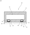
- FIG. 7 shows an embodiment of the present invention having a structure that is electrically and mechanically connected to a connection object via a bonding material formed by sintering the copper particle paste produced as described above. It is a figure which shows the electronic component module concerning (Embodiment 1).
- the electronic component module 30 has a gold bump (external terminal) 33 formed on a surface electrode 32 of an IC chip (electronic component in the present invention) 31 and a copper sintered body (joining material).
- 34 is electrically and mechanically connected to a mounting electrode (connection object) 36 made of, for example, copper, formed on the circuit board 35, and the IC chip (electronic component) 31 is sealed.
- FIG. 7 shows a structure in which the IC chip 31 is mounted on the circuit board 35, for example, other electronic components such as a chip capacitor and a chip resistor may be mounted.
- the copper sintered body 34 which is the above-mentioned bonding material, is formed by baking the above-described copper particle paste, and the sintered copper body has an average crystallite diameter after sintering in the range of 60 to 150 nm. It is.
- a method for manufacturing the electronic component module 30 will be described.
- a circuit board 35 having a mounting electrode (land electrode) 36 on its surface is prepared.
- an IC chip (electronic component in the present invention) 31 having a gold bump (external terminal) 33 formed on the surface electrode 32 is prepared.
- the above-described copper particle paste is applied on the mounting electrode 36 of the circuit board 35, and the gold bump (external terminal) 33 of the IC chip (electronic component) 31 is applied on the mounting electrode 36 of the circuit board 35.
- the IC chip (electronic component) 31 is mounted on the mounting electrode 36 of the circuit board 35 so as to be positioned on the copper particle paste.
- the copper particles contained in the copper particle paste are fired by firing at 230 ° C. in a nitrogen atmosphere (inert atmosphere) without pressing the IC chip (electronic component) 31 toward the circuit board 35.
- the gold bumps (external terminals) 33 are connected to the mounting electrodes (connection objects) 36 via the copper sintered body (bonding material) 34.
- This electronic component module 30 is formed by baking a gold bump (external terminal 33) of the above-mentioned copper particle paste on an IC chip (electronic component) 31, and has an average crystallite diameter after sintering in the range of 60 to 150 nm. It has a structure in which it is electrically and mechanically connected to a mounting electrode (connection object) 36 of a circuit board 35 to be connected through a copper sintered body (bonding material) 34.
- the gold bumps (external terminals) 33 and the mounting electrodes (connection objects) 36 of the IC chip (electronic component) 31 have a high density and a bonding material 34 made of a copper sintered body with a small proportion of voids. Thus, it is possible to provide a highly reliable electronic component module that is securely bonded.
- the gold bump (external terminal) 33 of the IC chip (electronic component) 31 is connected to the connection target 36 via the copper particle paste that becomes the copper sintered body 34 after firing. Since the heat treatment is performed with the IC chip (electronic component) 31 and the mounting electrode (connection target) 36 positioned so as to face each other, the gold bump (external) of the IC chip (electronic component) 31 is provided.
- the terminal 33 and the connection object 36 can be reliably bonded by the bonding material (copper sintered body) 34 made of a copper sintered body having a high density and a small proportion of voids.
- the bump of the IC chip is made of gold
- the mounting electrode (land electrode) is made of copper.
- Ag, Cu, Ni, Ag—Pd, etc. and as the constituent material of the mounting electrode (land electrode), Au, Ag, Ni, Ag—Pd, etc. can be used. Is possible.
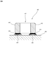
- FIG. 8 is a diagram showing an electronic component module according to an embodiment (Embodiment 2) of the present invention.
- an external terminal 42 made of copper included in the multilayer ceramic capacitor 41 is formed on a circuit board (alumina substrate) 45 via a copper sintered body (bonding material) 44.
- This is an electronic component module having a structure electrically and mechanically connected to the mounting electrode 46 (connection object in the present invention) 46 made of copper.
- the bonding strength between the mounting electrode (land electrode) 46 and the external terminal 42 is 45 MPa.
- a copper particle paste that becomes a sintered copper body 44 after firing is applied onto a mounting electrode (land electrode) 46 formed on the surface of a circuit board 45, and external terminals 42 are formed at both ends.
- the laminated ceramic capacitor 41 is placed so that the mounting electrode (land electrode) 46 and the external terminal 42 are opposed to each other with the copper particle paste interposed therebetween, and in particular, a nitrogen atmosphere (without applying stress from the outside) It is formed by sintering the copper particles contained in the copper particle paste by firing at 230 ° C. in an inert atmosphere.
- FIG. 9 is a micrograph (SEM image) of the vicinity of the joint between the multilayer ceramic capacitor 41 and the circuit board 45. From FIG. 9, the external terminal 42 made of copper of the multilayer ceramic capacitor 41 is bonded to the mounting electrode 46 made of copper on the circuit board 45 via the bonding material made of the copper sintered body 44. I understand.
- the external terminal 42 made of copper of the multilayer ceramic capacitor 41 is formed by using the above copper particle paste without forming the Sn plating layer or the solder plating layer on the external terminal 42 of the multilayer ceramic capacitor 41. It can be seen that by directly bonding the mounting electrode 46 made of copper on the circuit board 45, highly reliable bonding can be realized without forming an intermetallic compound.
- the constituent material of the external terminal of the multilayer ceramic capacitor is not limited to copper, and may be formed of gold, silver, silver-palladium, nickel, or the like. Moreover, glass may be contained in copper.
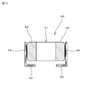
- FIG. 10 is a diagram illustrating an electronic component with a metal terminal (an electronic component module in a broad sense) according to another embodiment (third embodiment) of the present invention.
- An electronic component (for example, a multilayer ceramic capacitor) 50 shown in FIG. 10 has a copper sintered body (a copper sintered body) formed by baking the copper particle paste on the external electrode 52 formed on the surface of the electronic component element 51.
- the copper particle paste is applied to at least one of the external electrode 52 and the metal terminal 53 formed on the surface of the electronic component element 51, and the both are joined. In this state, heat treatment is performed under predetermined conditions to sinter the copper particles in the copper particle paste, so that it can be easily and reliably produced.
- this electronic component 50 with a metal terminal is a bonding material (made of a copper sintered body in which the external electrode 52 of the electronic component element 51 and the metal terminal 53 to be connected have a high density and a small proportion of voids) It is reliably joined by a copper sintered body) 54 and has high reliability.
- a metal terminal is not restricted to the thing of the above structures, The metal terminal which comprises some other electronic components may be sufficient. In that case, the same effect can be obtained.
- the constituent material of the metal terminal 53 There is no particular restriction on the constituent material of the metal terminal 53, and it is possible to use a material made of gold, silver, copper, silver-palladium, nickel, or the like.
- the copper particle paste is not limited to the electronic component module described in the first and second embodiments and the electronic component with a metal terminal described in the third embodiment (broadly defined electronic component module).
- A a connection material for built-in components disposed inside the multilayer ceramic substrate;
- B a material for forming a via-hole conductor for interlayer connection;
- C an electrode forming material for forming a wiring or an electrode;
- D a conductive sealing material,
- It can also be applied to applications such as connection materials for die bonding.
- Copper particles 11 Crystallites 12 Oxide film (copper oxide) 13 Organic compounds that exhibit reducing action (solvents) 21 First oxygen-free copper sample piece 22 Second oxygen-free copper sample piece 23 Copper sintered body obtained by firing copper particle paste 24 Share tool 30 Electronic component module 31 IC chip (electronic component) 32 Surface electrode 33 Gold bump (external terminal) 34 Copper sintered body (joining material) 35 Circuit board 36 Mounting electrode (target) 37 Sealing resin 40 Electronic component module 41 Multilayer ceramic capacitor 42 External terminal 44 Copper sintered body (joining material) 45 Circuit board (alumina substrate) 46 Mounting electrode (target) 50 Electronic component 51 Electronic component element 52 External electrode 53 Metal terminal 54 Copper sintered body (joining material)
Landscapes
- Engineering & Computer Science (AREA)
- Chemical & Material Sciences (AREA)
- Microelectronics & Electronic Packaging (AREA)
- Manufacturing & Machinery (AREA)
- Dispersion Chemistry (AREA)
- Spectroscopy & Molecular Physics (AREA)
- Composite Materials (AREA)
- Physics & Mathematics (AREA)
- Materials Engineering (AREA)
- Mechanical Engineering (AREA)
- Nanotechnology (AREA)
- Powder Metallurgy (AREA)
- Conductive Materials (AREA)
- Electric Connection Of Electric Components To Printed Circuits (AREA)
- Wire Bonding (AREA)
Abstract
Description
そして、表面実装型の電子部品(以下、単に電子部品という)を回路基板上に実装するにあたって、導電性の接合材料を用いて電子部品の外部端子を、回路基板に配設された実装用電極(接続対象)に機械的、電気的に接続することが行われている。
特許文献1はその他にも、上記焼結性接合材料を用いて電子部品を接合する場合に、電子部品を接合する方向に加圧しながら焼結熱処理を施すことを開示している。
電子部品が備える外部端子が、接合材料を介して、接続対象に電気的および機械的に接続された構造を有する電子部品モジュールであって、
前記接合材料は、
粒径分布の粒径ピークが0.1~5.0μmの範囲にあるとともに、焼結前の平均結晶子径が30~100nmの範囲にあり、かつ、凝集を抑制する分散剤を粒子表面に有していない銅粒子と、
前記銅粒子を焼結させる際の焼成温度で還元作用を奏する有機化合物と、
を含有する銅粒子ペーストを焼結させることにより形成されたものであること
を特徴としている。
焼結後の平均結晶子径が60~150nmとなるようにすることにより、安定した銅焼結体が形成される。
銅粒子を焼結させるための焼成温度で還元作用を奏する有機化合物として、ヒドロキシ基を有する有機化合物を用いることにより、焼成工程で銅粒子の表面に形成されている酸化物膜を除去すること、焼成工程で銅が酸化されることなく確実に焼結されるようにすることが可能になり、本発明をより実効あらしめることができる。
上記群からなる少なくとも1種を用いることにより、本発明をより実効あらしめることができる。
本発明の方法で電子部品の外部端子を回路基板上の実装用電極に接続することにより、例えば、ICチップや積層セラミックコンデンサなどの表面実装型の電子部品が回路基板上に搭載された構造を有する、信頼性の高い電子部品モジュールを確実に製造することが可能になる。
本発明の方法で電子部品の外部端子を金属端子に取り付けることにより、信頼性の高い端子付き電子部品モジュールを確実に製造することが可能になる。
電子部品が備える外部端子が、接合材料を介して接続対象に電気的および機械的に接続された構造を有する電子部品モジュールの製造方法であって、
前記電子部品の前記外部端子が、粒径分布の粒径ピークが0.1~5.0μmの範囲にあるとともに、焼結前の平均結晶子径が30~100nmの範囲にあり、かつ、凝集を抑制する分散剤を粒子表面に有していない銅粒子と、前記銅粒子を焼結させる際の焼成温度で還元作用を奏する有機化合物と、を含有する銅粒子ペーストを介して前記接続対象と対向するように、前記電子部品と前記接合対象とを位置させる工程と、
熱処理を行って前記銅粒子ペーストに含まれる前記銅粒子を焼結させることにより、銅粒子の平均結晶子径が60~150nmである銅焼結体を形成し、前記電子部品の前記外部端子と前記接続対象とを、前記銅焼結体を介して接合する工程と
を備えていることを特徴としている。
不活性雰囲気で熱処理することにより、さらに確実に銅粒子ペーストを構成する銅粒子を焼結させることが可能になり、本発明をより実効あらしめることができる。
図1A~図1Dは、銅粒子の焼結のプロセスを模式的に示す図である。
上記の銅粒子ペーストを構成する銅粒子は、このようなメカニズムにより、低温でも効率よく焼結させることができる。
本発明の実施形態1にかかる電子部品モジュールは、電子部品が備える外部端子が、銅粒子ペーストを焼結することにより形成される接合材料を介して、接続対象に電気的および機械的に接続された構造を有する電子部品モジュールである。
接合材料となる銅粒子ペーストを作製するにあたって、まず銅粒子として粒度分布の粒径ピークが0.1~5.0μmの範囲にあり、かつ、焼結前の平均結晶子径が30~100nmの範囲にある銅粒子を用意した。
(1)接合強度
上述のようにして作製した銅粒子ペーストを用いて、以下に説明する方法で、無酸素銅試料片どうしを接合し、接合強度を調べた。
その結果、シェア強度として、36MPaの高強度が得られることが確認された。
焼成前の平均結晶子径は、銅粒子ペーストをガラス板上にインクを塗布し、上述の方法、すなわち、X線回折測定を行って得たピーク<111>、<200>、<311>の3つのピークから、リートベルト法により結晶子径を算出しその平均値を求める方法で測定した。焼成後の平均結晶子径は、シェアした後の焼結体を、ピンセットを用いて抽出し、ガラス板に載せて、上述の方法、すなわち、X線回折測定を行って得たピーク<111>、<200>、<311>の3つのピークから、リートベルト法により結晶子径を算出しその平均値を求める方法で測定した。
これに対して、図4A、図4Bからわかるように、平均結晶子径が56.7nmの銅粒子10を用いた本発明の要件において規定されている範囲内にある銅粒子ペーストの場合、銅粒子10がネック成長すること、すなわち十分に焼結することが確認された。
上述の銅粒子ペーストにおいて、銅粒子を焼結させる際の焼成温度で還元作用を奏する有機化合物(溶剤)として用いたトリエタノールアミンの還元性を、以下の方法で調べた。
この電子部品モジュール30は、図7に示すように、ICチップ(本発明における電子部品)31の表面電極32上に形成された金バンプ(外部端子)33が、銅焼結体(接合材料)34を介して、回路基板35に形成された、例えば銅からなる実装用電極(接続対象)36上に、電気的および機械的に接続されているとともに、ICチップ(電子部品)31が封止樹脂37により封止された構造を有する電子部品モジュールである。
また、表面電極32上に金バンプ(外部端子)33が形成されたICチップ(本発明における電子部品)31を用意する。
図8は、本発明の実施形態(実施形態2)にかかる電子部品モジュールを示す図である。
この電子部品モジュール40は、図8に示すように、積層セラミックコンデンサ41が備える銅からなる外部端子42が、銅焼結体(接合材料)44を介して、回路基板(アルミナ基板)45に形成された銅からなる実装用電極(本発明における接続対象)46に、電気的および機械的に接続された構造を有する電子部品モジュールである。
図9より、回路基板45上の銅からなる実装用電極46に対して、積層セラミックコンデンサ41の銅からなる外部端子42が、銅焼結体44からなる接合材料を介して接合されていることがわかる。
図10は、本発明の他の実施形態(実施形態3)にかかる金属端子付きの電子部品(広義の電子部品モジュール)を示す図である。
なお、金属端子は上述のような構成のものに限られるものではなく、他の電子部品の一部を構成する金属端子であってもよい。その場合も同様の効果を得ることができる。金属端子53の構成材料に特別の制約はなく、金、銀、銅、銀-パラジウム、ニッケルなどからなるものを用いることが可能である。
(a)多層セラミック基板の内部に配設される内蔵部品の接続材料、
(b)層間接続のためのビアホール導体形成用材料、
(c)配線や電極を形成するための電極形成用材料、
(d)導電性封止材料、
(e)ダイボンド用の接続材料
などの用途にも適用することが可能である。
11 結晶子
12 酸化膜(銅酸化物)
13 還元作用を奏する有機化合物(溶剤)
21 第1の無酸素銅試料片
22 第2の無酸素銅試料片
23 銅粒子ペーストを焼成してなる銅焼結体
24 シェアツール
30 電子部品モジュール
31 ICチップ(電子部品)
32 表面電極
33 金バンプ(外部端子)
34 銅焼結体(接合材料)
35 回路基板
36 実装用電極(接続対象)
37 封止樹脂
40 電子部品モジュール
41 積層セラミックコンデンサ
42 外部端子
44 銅焼結体(接合材料)
45 回路基板(アルミナ基板)
46 実装用電極(接続対象)
50 電子部品
51 電子部品素子
52 外部電極
53 金属端子
54 銅焼結体(接合材料)
Claims (9)
- 電子部品が備える外部端子が、接合材料を介して、接続対象に電気的および機械的に接続された構造を有する電子部品モジュールであって、
前記接合材料は、
粒径分布の粒径ピークが0.1~5.0μmの範囲にあるとともに、焼結前の平均結晶子径が30~100nmの範囲にあり、かつ、凝集を抑制する分散剤を粒子表面に有していない銅粒子と、
前記銅粒子を焼結させる際の焼成温度で還元作用を奏する有機化合物と、
を含有する銅粒子ペーストを焼結させることにより形成されたものであること
を特徴とする電子部品モジュール。 - 前記接合材料は、焼結後の銅粒子の平均結晶子径が60~150nmの範囲にある銅焼結体であること
を特徴とする請求項1記載の電子部品モジュール。 - 前記有機化合物がヒドロキシ基を有する有機化合物であることを特徴とする請求項1または2記載の電子部品モジュール。
- 前記有機化合物がトリエタノールアミン、グリセリン、エチレングリコール、トリエチレングリコール、ジエチレングリコール、ジプロピレングリコールからなる群より選ばれる少なくとも1種を含むことを特徴とする請求項1~3のいずれかに記載の電子部品モジュール。
- 前記接続対象が、回路基板に配設された実装用電極であることを特徴とする請求項1~4のいずれかに記載の電子部品モジュール。
- 前記接続対象が、前記外部端子に取り付けられた金属端子であることを特徴とする請求項1~4のいずれかに記載の電子部品モジュール。
- 電子部品が備える外部端子が、接合材料を介して接続対象に電気的および機械的に接続された構造を有する電子部品モジュールの製造方法であって、
前記電子部品の前記外部端子が、粒径分布の粒径ピークが0.1~5.0μmの範囲にあるとともに、焼結前の平均結晶子径が30~100nmの範囲にあり、かつ、凝集を抑制する分散剤を粒子表面に有していない銅粒子と、前記銅粒子を焼結させる際の焼成温度で還元作用を奏する有機化合物と、を含有する銅粒子ペーストを介して前記接続対象と対向するように、前記電子部品と前記接合対象とを位置させる工程と、
熱処理を行って前記銅粒子ペーストに含まれる前記銅粒子を焼結させることにより、銅粒子の平均結晶子径が60~150nmである銅焼結体を形成し、前記電子部品の前記外部端子と前記接続対象とを、前記銅焼結体を介して接合する工程と
を備えていることを特徴とする電子部品モジュールの製造方法。 - 前記電子部品の前記外部端子が、前記銅粒子ペーストを介して前記接続対象と対向するように前記電子部品を前記接合対象上に載置した状態で、外部から力を加えることなく前記熱処理を行うことを特徴とする請求項7記載の電子部品モジュールの製造方法。
- 前記熱処理を、不活性雰囲気中で実施することを特徴とする請求項7または8記載の電子部品モジュールの製造方法。
Priority Applications (4)
| Application Number | Priority Date | Filing Date | Title |
|---|---|---|---|
| CN201580007207.4A CN106170851B (zh) | 2014-02-04 | 2015-01-26 | 电子元器件模块、以及电子元器件模块的制造方法 |
| JP2015560928A JP6337909B2 (ja) | 2014-02-04 | 2015-01-26 | 電子部品モジュールの製造方法 |
| EP15746474.4A EP3104400B1 (en) | 2014-02-04 | 2015-01-26 | Manufacturing method of electronic component module |
| US15/225,379 US9860989B2 (en) | 2014-02-04 | 2016-08-01 | Electronic component module and method for manufacturing electronic component module |
Applications Claiming Priority (2)
| Application Number | Priority Date | Filing Date | Title |
|---|---|---|---|
| JP2014019212 | 2014-02-04 | ||
| JP2014-019212 | 2014-02-04 |
Related Child Applications (1)
| Application Number | Title | Priority Date | Filing Date |
|---|---|---|---|
| US15/225,379 Continuation US9860989B2 (en) | 2014-02-04 | 2016-08-01 | Electronic component module and method for manufacturing electronic component module |
Publications (1)
| Publication Number | Publication Date |
|---|---|
| WO2015118982A1 true WO2015118982A1 (ja) | 2015-08-13 |
Family
ID=53777789
Family Applications (1)
| Application Number | Title | Priority Date | Filing Date |
|---|---|---|---|
| PCT/JP2015/052018 Ceased WO2015118982A1 (ja) | 2014-02-04 | 2015-01-26 | 電子部品モジュール、および電子部品モジュールの製造方法 |
Country Status (5)
| Country | Link |
|---|---|
| US (1) | US9860989B2 (ja) |
| EP (1) | EP3104400B1 (ja) |
| JP (1) | JP6337909B2 (ja) |
| CN (1) | CN106170851B (ja) |
| WO (1) | WO2015118982A1 (ja) |
Cited By (8)
| Publication number | Priority date | Publication date | Assignee | Title |
|---|---|---|---|---|
| JP2017152638A (ja) * | 2016-02-26 | 2017-08-31 | 株式会社村田製作所 | 接合構造、該接合構造を備えた電子部品、および該接合構造の形成方法 |
| WO2018074188A1 (ja) * | 2016-10-19 | 2018-04-26 | 株式会社村田製作所 | インダクタ部品、インダクタ部品の製造方法 |
| EP3358610A4 (en) * | 2015-10-02 | 2019-04-24 | Mitsui Mining and Smelting Co., Ltd. | BONDING CONNECTION STRUCTURE |
| JP2020136580A (ja) * | 2019-02-22 | 2020-08-31 | 株式会社大阪ソーダ | 導電性接着剤を用いる接合方法 |
| US11257779B2 (en) | 2017-05-26 | 2022-02-22 | Murata Manufacturing Co., Ltd. | Multilayer wiring board, electronic device and method for producing multilayer wiring board |
| JPWO2023189338A1 (ja) * | 2022-03-30 | 2023-10-05 | ||
| JPWO2023189513A1 (ja) * | 2022-03-30 | 2023-10-05 | ||
| WO2024248066A1 (ja) * | 2023-05-30 | 2024-12-05 | 株式会社ダイセル | ポリマー及びそれを含む感光性樹脂組成物、銅ペースト、液状組成物、半導体デバイスの製造方法及び半導体接続用銅ピラーの製造方法 |
Families Citing this family (13)
| Publication number | Priority date | Publication date | Assignee | Title |
|---|---|---|---|---|
| JP6332566B2 (ja) | 2015-09-15 | 2018-05-30 | 株式会社村田製作所 | 接合用部材、接合用部材の製造方法、および、接合方法 |
| WO2017056842A1 (ja) | 2015-09-28 | 2017-04-06 | 株式会社村田製作所 | ヒートパイプ、放熱部品、ヒートパイプの製造方法 |
| JP6369640B2 (ja) * | 2015-11-05 | 2018-08-08 | 株式会社村田製作所 | 接合用部材、および、接合用部材の製造方法 |
| JP6565710B2 (ja) * | 2016-01-27 | 2019-08-28 | 三菱マテリアル株式会社 | 銅部材接合体の製造方法 |
| CN112771628B (zh) | 2018-09-28 | 2022-09-13 | 纳美仕有限公司 | 导电性糊剂 |
| EP3950175B1 (en) * | 2019-03-29 | 2025-06-04 | Mitsui Mining & Smelting Co., Ltd. | Bonding material and uses therof |
| CN110202137B (zh) * | 2019-05-29 | 2021-07-20 | 深圳第三代半导体研究院 | 一种低温烧结铜膏及其烧结工艺 |
| US20240081336A1 (en) * | 2019-09-16 | 2024-03-14 | Corning Incorporated | Color stabilization of biocidal coatings |
| KR102842071B1 (ko) * | 2019-09-18 | 2025-08-04 | 삼성전기주식회사 | 전자 부품 및 그 실장 기판 |
| JP7380256B2 (ja) | 2020-01-28 | 2023-11-15 | 三菱マテリアル株式会社 | 接合用シート |
| US20240224422A1 (en) * | 2021-01-28 | 2024-07-04 | Kyocera Corporation | Wiring board |
| EP4503103A4 (en) * | 2022-03-30 | 2025-07-02 | Mitsui Mining & Smelting Co Ltd | PROCESS FOR MANUFACTURING BODY BONDED |
| CN118973743A (zh) * | 2022-04-28 | 2024-11-15 | 三井金属矿业株式会社 | 接合用铜糊剂、被接合体的接合方法、接合体的制造方法和接合用铜糊剂的制造方法 |
Citations (2)
| Publication number | Priority date | Publication date | Assignee | Title |
|---|---|---|---|---|
| JP2004265607A (ja) * | 2003-01-23 | 2004-09-24 | Matsushita Electric Ind Co Ltd | 導電性ペースト、その導電性ペーストを用いた回路形成基板、およびその製造方法 |
| JP2013091835A (ja) * | 2011-10-27 | 2013-05-16 | Hitachi Ltd | 銅ナノ粒子を用いた焼結性接合材料及びその製造方法及び電子部材の接合方法 |
Family Cites Families (21)
| Publication number | Priority date | Publication date | Assignee | Title |
|---|---|---|---|---|
| US4859364A (en) * | 1988-05-25 | 1989-08-22 | E. I. Du Pont De Nemours And Company | Conductive paste composition |
| US5180523A (en) * | 1989-11-14 | 1993-01-19 | Poly-Flex Circuits, Inc. | Electrically conductive cement containing agglomerate, flake and powder metal fillers |
| US5652042A (en) * | 1993-10-29 | 1997-07-29 | Matsushita Electric Industrial Co., Ltd. | Conductive paste compound for via hole filling, printed circuit board which uses the conductive paste |
| JPH09198920A (ja) * | 1996-01-22 | 1997-07-31 | Mitsuboshi Belting Ltd | 銅導体ペースト及び該銅導体ペーストを印刷した基板 |
| US6679937B1 (en) * | 1997-02-24 | 2004-01-20 | Cabot Corporation | Copper powders methods for producing powders and devices fabricated from same |
| US6139777A (en) * | 1998-05-08 | 2000-10-31 | Matsushita Electric Industrial Co., Ltd. | Conductive paste for filling via-hole, double-sided and multilayer printed circuit boards using the same, and method for producing the same |
| CN1273993C (zh) * | 1998-08-28 | 2006-09-06 | 松下电器产业株式会社 | 导电粘结结构,含该结构的制品及其制造方法 |
| US6620344B2 (en) * | 1999-05-28 | 2003-09-16 | Dowa Mining Co., Ltd. | Copper particle clusters and powder containing the same suitable as conductive filler of conductive paste |
| JP2002110444A (ja) * | 2000-09-26 | 2002-04-12 | Murata Mfg Co Ltd | 導電性ペーストおよび積層セラミック電子部品 |
| JP3854103B2 (ja) * | 2001-06-28 | 2006-12-06 | 住友ベークライト株式会社 | 導電性ペースト及び該ペーストを用いてなる半導体装置 |
| JP4298597B2 (ja) * | 2004-07-01 | 2009-07-22 | 日東電工株式会社 | 配線回路基板および配線回路基板の製造方法 |
| KR100702595B1 (ko) * | 2005-07-22 | 2007-04-02 | 삼성전기주식회사 | 금속 나노 입자 및 이의 제조방법 |
| JP4687599B2 (ja) | 2006-07-26 | 2011-05-25 | 住友金属鉱山株式会社 | 銅微粉とその製造方法及び導電性ペースト |
| JP5525301B2 (ja) * | 2010-03-24 | 2014-06-18 | 国立大学法人東北大学 | 金属微粒子・金属酸化物微粒子の製造方法、金属微粒子・金属酸化物微粒子、並びに金属含有ペーストおよび金属膜・金属酸化物膜 |
| JP5520861B2 (ja) * | 2010-03-26 | 2014-06-11 | 古河電気工業株式会社 | 銅合金微粒子分散液、焼結導電体の製造方法、及び焼結導電体、並びに導電接続部材 |
| JP2012038790A (ja) | 2010-08-04 | 2012-02-23 | Hitachi Ltd | 電子部材ならびに電子部品とその製造方法 |
| JP5557698B2 (ja) | 2010-11-04 | 2014-07-23 | 株式会社日立製作所 | 焼結接合剤、その製造方法およびそれを用いた接合方法 |
| KR101719189B1 (ko) * | 2011-04-04 | 2017-03-23 | 파나소닉 아이피 매니지먼트 가부시키가이샤 | 실장구조체 및 그 제조방법 |
| JP2013008907A (ja) | 2011-06-27 | 2013-01-10 | Hitachi Chem Co Ltd | 導電性ペースト用酸化銅粉末、導電性ペースト用酸化銅粉末の製造方法、導電性ペースト及びこれを用いて得られる銅配線層 |
| WO2014080662A1 (ja) * | 2012-11-26 | 2014-05-30 | 三井金属鉱業株式会社 | 銅粉及びその製造方法 |
| KR102018194B1 (ko) * | 2014-08-29 | 2019-09-04 | 미쓰이금속광업주식회사 | 도전체의 접속 구조 및 그 제조 방법, 도전성 조성물 그리고 전자부품 모듈 |
-
2015
- 2015-01-26 JP JP2015560928A patent/JP6337909B2/ja active Active
- 2015-01-26 WO PCT/JP2015/052018 patent/WO2015118982A1/ja not_active Ceased
- 2015-01-26 CN CN201580007207.4A patent/CN106170851B/zh active Active
- 2015-01-26 EP EP15746474.4A patent/EP3104400B1/en active Active
-
2016
- 2016-08-01 US US15/225,379 patent/US9860989B2/en active Active
Patent Citations (2)
| Publication number | Priority date | Publication date | Assignee | Title |
|---|---|---|---|---|
| JP2004265607A (ja) * | 2003-01-23 | 2004-09-24 | Matsushita Electric Ind Co Ltd | 導電性ペースト、その導電性ペーストを用いた回路形成基板、およびその製造方法 |
| JP2013091835A (ja) * | 2011-10-27 | 2013-05-16 | Hitachi Ltd | 銅ナノ粒子を用いた焼結性接合材料及びその製造方法及び電子部材の接合方法 |
Non-Patent Citations (1)
| Title |
|---|
| See also references of EP3104400A4 * |
Cited By (12)
| Publication number | Priority date | Publication date | Assignee | Title |
|---|---|---|---|---|
| EP3358610A4 (en) * | 2015-10-02 | 2019-04-24 | Mitsui Mining and Smelting Co., Ltd. | BONDING CONNECTION STRUCTURE |
| US10340154B2 (en) | 2015-10-02 | 2019-07-02 | Mitsui Mining & Smelting Co., Ltd. | Bonding junction structure |
| JP2017152638A (ja) * | 2016-02-26 | 2017-08-31 | 株式会社村田製作所 | 接合構造、該接合構造を備えた電子部品、および該接合構造の形成方法 |
| WO2018074188A1 (ja) * | 2016-10-19 | 2018-04-26 | 株式会社村田製作所 | インダクタ部品、インダクタ部品の製造方法 |
| US11257779B2 (en) | 2017-05-26 | 2022-02-22 | Murata Manufacturing Co., Ltd. | Multilayer wiring board, electronic device and method for producing multilayer wiring board |
| JP2020136580A (ja) * | 2019-02-22 | 2020-08-31 | 株式会社大阪ソーダ | 導電性接着剤を用いる接合方法 |
| JP7170968B2 (ja) | 2019-02-22 | 2022-11-15 | 株式会社大阪ソーダ | 導電性接着剤を用いる接合方法 |
| JPWO2023189338A1 (ja) * | 2022-03-30 | 2023-10-05 | ||
| JPWO2023189513A1 (ja) * | 2022-03-30 | 2023-10-05 | ||
| WO2023189513A1 (ja) * | 2022-03-30 | 2023-10-05 | 京セラ株式会社 | 配線基板 |
| US12598700B2 (en) | 2022-03-30 | 2026-04-07 | Kyocera Corporation | Wiring board |
| WO2024248066A1 (ja) * | 2023-05-30 | 2024-12-05 | 株式会社ダイセル | ポリマー及びそれを含む感光性樹脂組成物、銅ペースト、液状組成物、半導体デバイスの製造方法及び半導体接続用銅ピラーの製造方法 |
Also Published As
| Publication number | Publication date |
|---|---|
| EP3104400A4 (en) | 2017-11-15 |
| CN106170851A (zh) | 2016-11-30 |
| JP6337909B2 (ja) | 2018-06-06 |
| US20160338201A1 (en) | 2016-11-17 |
| CN106170851B (zh) | 2019-03-08 |
| JPWO2015118982A1 (ja) | 2017-03-23 |
| EP3104400A1 (en) | 2016-12-14 |
| EP3104400B1 (en) | 2022-08-31 |
| US9860989B2 (en) | 2018-01-02 |
Similar Documents
| Publication | Publication Date | Title |
|---|---|---|
| JP6337909B2 (ja) | 電子部品モジュールの製造方法 | |
| KR102097368B1 (ko) | 도전체의 접속 구조 및 그 제조 방법, 도전성 조성물 그리고 전자부품 모듈 | |
| JP6153077B2 (ja) | 金属ナノ粒子ペースト、それを含有する接合材料、およびそれを用いた半導体装置 | |
| KR20130061671A (ko) | 도전성 페이스트, 및 이 페이스트로부터 얻어지는 도전접속부재 | |
| TWI808208B (zh) | 用於燒結黏晶及類似應用之奈米銅糊及膜及製造燒結粉末的方法 | |
| JP6372978B2 (ja) | 導電性ペースト | |
| WO2014129626A1 (ja) | 接続構造体、及び半導体装置 | |
| KR20210068468A (ko) | 접합 재료용 입자 및 그 제조 방법, 접합용 페이스트 및 그 조제 방법, 그리고 접합체의 제조 방법 | |
| JP2013207213A (ja) | 電子部品モジュール及びその製造方法 | |
| JP6032110B2 (ja) | 金属ナノ粒子材料、それを含有する接合材料、およびそれを用いた半導体装置 | |
| CN114829036B (zh) | 银膏及接合体的制造方法 | |
| KR102307809B1 (ko) | 도전성 페이스트, 적층체, 및 Cu 기판 또는 Cu 전극과 도전체와의 접합 방법 | |
| JP5733638B2 (ja) | 接合材料およびそれを用いた半導体装置、ならびに配線材料およびそれを用いた電子素子用配線 | |
| JP6851810B2 (ja) | 加熱接合材及び電気電子機器の製造方法 | |
| CN116806177B (zh) | 接合用浆料、接合层、接合体及接合体的制造方法 | |
| JP7155654B2 (ja) | 接合体の製造方法 | |
| WO2014002949A1 (ja) | 接合基板及びその製造方法ならびに接合基板を用いた半導体モジュール及びその製造方法 | |
| JP7317397B2 (ja) | 酸化銅ペースト及び電子部品の製造方法 | |
| KR20200127165A (ko) | 금속 입자 응집체 및 그 제조 방법 그리고 페이스트상 금속 입자 응집체 조성물 및 이것을 사용한 접합체의 제조 방법 | |
| JP2006120973A (ja) | 回路基板および回路基板の製造方法 | |
| JP2017152638A (ja) | 接合構造、該接合構造を備えた電子部品、および該接合構造の形成方法 | |
| JP7024671B2 (ja) | 接合用ペーストを用いて被接合部材を接合する方法 | |
| JP7024670B2 (ja) | 接合用ペーストを用いて被接合部材を接合する方法 | |
| EP4657516A1 (en) | Conductive paste and bonding method using same | |
| TWI789698B (zh) | 氧化銅糊料及電子零件之製造方法 |
Legal Events
| Date | Code | Title | Description |
|---|---|---|---|
| 121 | Ep: the epo has been informed by wipo that ep was designated in this application |
Ref document number: 15746474 Country of ref document: EP Kind code of ref document: A1 |
|
| ENP | Entry into the national phase |
Ref document number: 2015560928 Country of ref document: JP Kind code of ref document: A |
|
| REEP | Request for entry into the european phase |
Ref document number: 2015746474 Country of ref document: EP |
|
| WWE | Wipo information: entry into national phase |
Ref document number: 2015746474 Country of ref document: EP |
|
| NENP | Non-entry into the national phase |
Ref country code: DE |