WO2015122319A1 - 発光モジュール、接続具、並びに発光モジュールの取付構造 - Google Patents
発光モジュール、接続具、並びに発光モジュールの取付構造 Download PDFInfo
- Publication number
- WO2015122319A1 WO2015122319A1 PCT/JP2015/052959 JP2015052959W WO2015122319A1 WO 2015122319 A1 WO2015122319 A1 WO 2015122319A1 JP 2015052959 W JP2015052959 W JP 2015052959W WO 2015122319 A1 WO2015122319 A1 WO 2015122319A1
- Authority
- WO
- WIPO (PCT)
- Prior art keywords
- light emitting
- connection
- power supply
- light
- panel
- Prior art date
- Legal status (The legal status is an assumption and is not a legal conclusion. Google has not performed a legal analysis and makes no representation as to the accuracy of the status listed.)
- Ceased
Links
Images








Classifications
-
- F—MECHANICAL ENGINEERING; LIGHTING; HEATING; WEAPONS; BLASTING
- F21—LIGHTING
- F21S—NON-PORTABLE LIGHTING DEVICES; SYSTEMS THEREOF; VEHICLE LIGHTING DEVICES SPECIALLY ADAPTED FOR VEHICLE EXTERIORS
- F21S8/00—Lighting devices intended for fixed installation
- F21S8/04—Lighting devices intended for fixed installation intended only for mounting on a ceiling or the like overhead structures
-
- F—MECHANICAL ENGINEERING; LIGHTING; HEATING; WEAPONS; BLASTING
- F21—LIGHTING
- F21S—NON-PORTABLE LIGHTING DEVICES; SYSTEMS THEREOF; VEHICLE LIGHTING DEVICES SPECIALLY ADAPTED FOR VEHICLE EXTERIORS
- F21S8/00—Lighting devices intended for fixed installation
- F21S8/04—Lighting devices intended for fixed installation intended only for mounting on a ceiling or the like overhead structures
- F21S8/043—Lighting devices intended for fixed installation intended only for mounting on a ceiling or the like overhead structures mounted by means of a rigid support, e.g. bracket or arm
-
- F—MECHANICAL ENGINEERING; LIGHTING; HEATING; WEAPONS; BLASTING
- F21—LIGHTING
- F21V—FUNCTIONAL FEATURES OR DETAILS OF LIGHTING DEVICES OR SYSTEMS THEREOF; STRUCTURAL COMBINATIONS OF LIGHTING DEVICES WITH OTHER ARTICLES, NOT OTHERWISE PROVIDED FOR
- F21V17/00—Fastening of component parts of lighting devices, e.g. shades, globes, refractors, reflectors, filters, screens, grids or protective cages
- F21V17/10—Fastening of component parts of lighting devices, e.g. shades, globes, refractors, reflectors, filters, screens, grids or protective cages characterised by specific fastening means or way of fastening
- F21V17/105—Fastening of component parts of lighting devices, e.g. shades, globes, refractors, reflectors, filters, screens, grids or protective cages characterised by specific fastening means or way of fastening using magnets
-
- F—MECHANICAL ENGINEERING; LIGHTING; HEATING; WEAPONS; BLASTING
- F21—LIGHTING
- F21V—FUNCTIONAL FEATURES OR DETAILS OF LIGHTING DEVICES OR SYSTEMS THEREOF; STRUCTURAL COMBINATIONS OF LIGHTING DEVICES WITH OTHER ARTICLES, NOT OTHERWISE PROVIDED FOR
- F21V17/00—Fastening of component parts of lighting devices, e.g. shades, globes, refractors, reflectors, filters, screens, grids or protective cages
- F21V17/10—Fastening of component parts of lighting devices, e.g. shades, globes, refractors, reflectors, filters, screens, grids or protective cages characterised by specific fastening means or way of fastening
- F21V17/16—Fastening of component parts of lighting devices, e.g. shades, globes, refractors, reflectors, filters, screens, grids or protective cages characterised by specific fastening means or way of fastening by deformation of parts; Snap action mounting
- F21V17/164—Fastening of component parts of lighting devices, e.g. shades, globes, refractors, reflectors, filters, screens, grids or protective cages characterised by specific fastening means or way of fastening by deformation of parts; Snap action mounting the parts being subjected to bending, e.g. snap joints
-
- F—MECHANICAL ENGINEERING; LIGHTING; HEATING; WEAPONS; BLASTING
- F21—LIGHTING
- F21V—FUNCTIONAL FEATURES OR DETAILS OF LIGHTING DEVICES OR SYSTEMS THEREOF; STRUCTURAL COMBINATIONS OF LIGHTING DEVICES WITH OTHER ARTICLES, NOT OTHERWISE PROVIDED FOR
- F21V21/00—Supporting, suspending, or attaching arrangements for lighting devices; Hand grips
- F21V21/14—Adjustable mountings
- F21V21/26—Pivoted arms
- F21V21/28—Pivoted arms adjustable in more than one plane
- F21V21/29—Pivoted arms adjustable in more than one plane employing universal joints
-
- F—MECHANICAL ENGINEERING; LIGHTING; HEATING; WEAPONS; BLASTING
- F21—LIGHTING
- F21V—FUNCTIONAL FEATURES OR DETAILS OF LIGHTING DEVICES OR SYSTEMS THEREOF; STRUCTURAL COMBINATIONS OF LIGHTING DEVICES WITH OTHER ARTICLES, NOT OTHERWISE PROVIDED FOR
- F21V23/00—Arrangement of electric circuit elements in or on lighting devices
- F21V23/003—Arrangement of electric circuit elements in or on lighting devices the elements being electronics drivers or controllers for operating the light source, e.g. for a LED array
-
- F—MECHANICAL ENGINEERING; LIGHTING; HEATING; WEAPONS; BLASTING
- F21—LIGHTING
- F21V—FUNCTIONAL FEATURES OR DETAILS OF LIGHTING DEVICES OR SYSTEMS THEREOF; STRUCTURAL COMBINATIONS OF LIGHTING DEVICES WITH OTHER ARTICLES, NOT OTHERWISE PROVIDED FOR
- F21V23/00—Arrangement of electric circuit elements in or on lighting devices
- F21V23/003—Arrangement of electric circuit elements in or on lighting devices the elements being electronics drivers or controllers for operating the light source, e.g. for a LED array
- F21V23/004—Arrangement of electric circuit elements in or on lighting devices the elements being electronics drivers or controllers for operating the light source, e.g. for a LED array arranged on a substrate, e.g. a printed circuit board
- F21V23/006—Arrangement of electric circuit elements in or on lighting devices the elements being electronics drivers or controllers for operating the light source, e.g. for a LED array arranged on a substrate, e.g. a printed circuit board the substrate being distinct from the light source holder
-
- F—MECHANICAL ENGINEERING; LIGHTING; HEATING; WEAPONS; BLASTING
- F21—LIGHTING
- F21V—FUNCTIONAL FEATURES OR DETAILS OF LIGHTING DEVICES OR SYSTEMS THEREOF; STRUCTURAL COMBINATIONS OF LIGHTING DEVICES WITH OTHER ARTICLES, NOT OTHERWISE PROVIDED FOR
- F21V23/00—Arrangement of electric circuit elements in or on lighting devices
- F21V23/02—Arrangement of electric circuit elements in or on lighting devices the elements being transformers, impedances or power supply units, e.g. a transformer with a rectifier
-
- F—MECHANICAL ENGINEERING; LIGHTING; HEATING; WEAPONS; BLASTING
- F21—LIGHTING
- F21V—FUNCTIONAL FEATURES OR DETAILS OF LIGHTING DEVICES OR SYSTEMS THEREOF; STRUCTURAL COMBINATIONS OF LIGHTING DEVICES WITH OTHER ARTICLES, NOT OTHERWISE PROVIDED FOR
- F21V23/00—Arrangement of electric circuit elements in or on lighting devices
- F21V23/06—Arrangement of electric circuit elements in or on lighting devices the elements being coupling devices, e.g. connectors
-
- H—ELECTRICITY
- H05—ELECTRIC TECHNIQUES NOT OTHERWISE PROVIDED FOR
- H05B—ELECTRIC HEATING; ELECTRIC LIGHT SOURCES NOT OTHERWISE PROVIDED FOR; CIRCUIT ARRANGEMENTS FOR ELECTRIC LIGHT SOURCES, IN GENERAL
- H05B44/00—Circuit arrangements for operating electroluminescent light sources
-
- H—ELECTRICITY
- H05—ELECTRIC TECHNIQUES NOT OTHERWISE PROVIDED FOR
- H05B—ELECTRIC HEATING; ELECTRIC LIGHT SOURCES NOT OTHERWISE PROVIDED FOR; CIRCUIT ARRANGEMENTS FOR ELECTRIC LIGHT SOURCES, IN GENERAL
- H05B45/00—Circuit arrangements for operating light-emitting diodes [LED]
- H05B45/60—Circuit arrangements for operating LEDs comprising organic material, e.g. for operating organic light-emitting diodes [OLED] or polymer light-emitting diodes [PLED]
-
- H—ELECTRICITY
- H10—SEMICONDUCTOR DEVICES; ELECTRIC SOLID-STATE DEVICES NOT OTHERWISE PROVIDED FOR
- H10K—ORGANIC ELECTRIC SOLID-STATE DEVICES
- H10K59/00—Integrated devices, or assemblies of multiple devices, comprising at least one organic light-emitting element covered by group H10K50/00
- H10K59/10—OLED displays
- H10K59/18—Tiled displays
-
- F—MECHANICAL ENGINEERING; LIGHTING; HEATING; WEAPONS; BLASTING
- F21—LIGHTING
- F21Y—INDEXING SCHEME ASSOCIATED WITH SUBCLASSES F21K, F21L, F21S and F21V, RELATING TO THE FORM OR THE KIND OF THE LIGHT SOURCES OR OF THE COLOUR OF THE LIGHT EMITTED
- F21Y2105/00—Planar light sources
-
- F—MECHANICAL ENGINEERING; LIGHTING; HEATING; WEAPONS; BLASTING
- F21—LIGHTING
- F21Y—INDEXING SCHEME ASSOCIATED WITH SUBCLASSES F21K, F21L, F21S and F21V, RELATING TO THE FORM OR THE KIND OF THE LIGHT SOURCES OR OF THE COLOUR OF THE LIGHT EMITTED
- F21Y2115/00—Light-generating elements of semiconductor light sources
- F21Y2115/10—Light-emitting diodes [LED]
- F21Y2115/15—Organic light-emitting diodes [OLED]
-
- F—MECHANICAL ENGINEERING; LIGHTING; HEATING; WEAPONS; BLASTING
- F21—LIGHTING
- F21Y—INDEXING SCHEME ASSOCIATED WITH SUBCLASSES F21K, F21L, F21S and F21V, RELATING TO THE FORM OR THE KIND OF THE LIGHT SOURCES OR OF THE COLOUR OF THE LIGHT EMITTED
- F21Y2115/00—Light-generating elements of semiconductor light sources
- F21Y2115/20—Electroluminescent [EL] light sources
-
- Y—GENERAL TAGGING OF NEW TECHNOLOGICAL DEVELOPMENTS; GENERAL TAGGING OF CROSS-SECTIONAL TECHNOLOGIES SPANNING OVER SEVERAL SECTIONS OF THE IPC; TECHNICAL SUBJECTS COVERED BY FORMER USPC CROSS-REFERENCE ART COLLECTIONS [XRACs] AND DIGESTS
- Y02—TECHNOLOGIES OR APPLICATIONS FOR MITIGATION OR ADAPTATION AGAINST CLIMATE CHANGE
- Y02B—CLIMATE CHANGE MITIGATION TECHNOLOGIES RELATED TO BUILDINGS, e.g. HOUSING, HOUSE APPLIANCES OR RELATED END-USER APPLICATIONS
- Y02B20/00—Energy efficient lighting technologies, e.g. halogen lamps or gas discharge lamps
- Y02B20/30—Semiconductor lamps, e.g. solid state lamps [SSL] light emitting diodes [LED] or organic LED [OLED]
Definitions
- the present invention relates to a light emitting module.
- the present invention particularly relates to a light emitting module incorporating an organic EL panel for illumination.
- the present invention also relates to a connector that constitutes a part of the light emitting module.
- this invention relates to the attachment structure of the light emitting module which attaches a light emitting module to an installation object surface.
- An organic EL panel generally includes a structure in which an organic EL element is stacked on a base material such as a glass substrate, and the organic EL element is sealed and a structure in which power is supplied to the organic EL element.
- the organic EL element has two or more light-transmitting electrodes facing each other, and a light emitting layer made of an organic compound is laminated between the electrodes. The organic EL panel emits light by the energy of recombination of electrically excited electrons and holes.
- the organic EL module uses a surface emitting organic EL panel and is a flat light source. Therefore, a plurality of organic EL modules may be laid on the installation target surface such as a ceiling and used as one illumination.
- the organic EL panel uses the energy of recombination of electrons and holes as described above, the amount of light emission changes with the amount of current passing between the electrodes. That is, since the internal resistance of the organic EL panel differs depending on the quality of the electrodes, the light emitting layer, etc., the amount of current passing between the electrodes is different and the amount of light emission is different. Therefore, even when manufactured on the same manufacturing line, individual differences may occur in quality. Although the influence on the light emission due to the individual difference of the electrical resistance value is very small, when dimming control of the organic EL module, precise dimming cannot be performed. In addition, when a plurality of organic EL modules are used while being laid in a planar shape, light and shade may occur between adjacent organic EL modules.
- an organic EL panel has a structure in which a control substrate having a semi-fixed resistor is provided to absorb individual differences between products. That is, an attempt has been made to adjust the amount of electric power supplied to the organic EL element by adjusting the electric resistance value with a semi-fixed resistor, and to eliminate individual differences in internal resistance between products as much as possible.
- a light source unit and a mounting unit attached to the non-light emitting surface side of the light source unit are provided, and the mounting unit controls the lighting of the light source unit, the circuit board, and an external device.
- An illumination device having a connection terminal to which a conductive wire for electrically connecting the two is connected is disclosed.
- the connection terminal is disposed inward of the outer peripheral end of the mounting surface of the light source unit in the mounting unit, and the light source unit and the mounting unit are connected with the mounting unit attached to the light source unit.
- each light emitting module is provided with a semiconductor memory that stores the characteristics of each light emitting element
- a method for controlling the power supplied to the light emitting element according to the characteristics of the light emitting element read from the semiconductor memory is disclosed.
- an output terminal is connected to a power supply terminal that supplies power to the light emitting element through a resistance element, and the power supplied to the light emitting element is feedback-controlled based on the output of the output terminal.
- a part of the resistance element is formed as a thin film resistor on the same substrate as the light-emitting element, and the resistance value of the resistor is adjusted by trimming, whereby the resistance value of the resistance element is individually determined. It is possible to adjust in advance according to the difference.
- control board for controlling the organic EL panel is also used for light control and the like.
- the control circuit of the control board differs depending on the control method such as dimming.
- the control board basically includes the same control circuit. Therefore, when performing the same control, there is a demand for using the same control board from the viewpoint of suppressing the cost.
- an object of the present invention is to provide a light emitting module that can absorb individual differences of organic EL panels that are inevitably produced in manufacturing and individual differences between different types of organic EL panels. Moreover, it aims at providing the connection tool of the organic electroluminescent panel used for the light emitting module. Furthermore, it aims at providing the attachment structure of the light emitting module for attaching a light emitting module to installation object surfaces, such as a ceiling.
- the present inventor attempted to increase the versatility of the control board by separately providing a control board that performs dimming control and an adjustment element for absorbing individual differences. It was. That is, by providing a part of the adjustment mechanism for absorbing the individual difference of the internal resistance on the organic EL panel side, the control board can be reused, and the manufacturing cost is reduced. Then, the present inventor considered that a plurality of types of organic EL panels can be used with one type of control board.
- the connector includes a connection side circuit, the connection side circuit includes a circuit side power supply path that contributes to power supply to the light emitting panel, and the light emitting panel includes an adjustment element and a light emitting element.
- the adjustment element is capable of adjusting an adjustment factor according to the characteristics of the light emitting element, and the adjustment element is a light emitting module electrically connected to the light emitting element through the circuit side power supply path. is there.
- the “installation target surface” here refers to a target surface on which the light emitting panel is to be installed, and specifically includes a ceiling, a wall surface, a floor surface, a crosspiece, and the like.
- the “adjustment factor” here is a variable factor such as an electric resistance value, a voltage value, a current value, an electric energy, and an amount of heat, and is a factor that contributes to power feeding to the light emitting element.
- the adjustment element capable of adjusting the adjustment factor such as the electric resistance value according to the characteristics of the light emitting element since the adjustment element capable of adjusting the adjustment factor such as the electric resistance value according to the characteristics of the light emitting element is provided, individual differences generated between the light emitting panels due to the manufacturing of the light emitting panel are adjusted by the adjusting element. can do. Therefore, it is possible to unify the amount of light emission among the light emitting panels, and it is possible to perform light control precisely even when control such as light control is performed. Further, according to this aspect, the adjustment element is provided on the light emitting panel side, and adjustment factors such as an electric resistance value can be adjusted using the adjustment element of the light emission panel. Therefore, it is not necessary to provide an adjustment element for absorbing individual differences in the connection tool, and the connection tool need not be formed in accordance with the type of the light-emitting panel. Therefore, according to this aspect, it becomes possible to use the connector formed in accordance with one light-emitting panel also in another light-emitting panel, and the manufacturing cost can be suppress
- a preferred aspect is that the adjusting element can adjust its own electrical resistance value.
- the characteristics of the light emitting panel can be easily adjusted.
- connection-side circuit further includes a supply-side power supply path that contributes to power supply to the light-emitting panel, and the supply-side power supply path is electrically in series with the circuit-side power supply path via the adjustment element.
- the adjustment element is electrically connected in series with the light emitting element via the circuit-side power supply path.
- the adjustment element capable of adjusting the adjustment factor such as the electric resistance value since the adjustment element capable of adjusting the adjustment factor such as the electric resistance value is provided, the individual difference generated between the light-emitting panels due to the manufacture of the light-emitting panel can be adjusted by the adjustment element. Therefore, it is possible to unify the amount of light emission among the light emitting panels, and it is possible to perform light control precisely even when control such as light control is performed. Further, according to this aspect, there is a path that returns from the supply side power supply path of the connection tool to the circuit side power supply path of the connection tool via the adjustment element of the light emitting panel. That is, one circuit is formed by using the connection side circuit provided in the connection tool and the adjustment element of the light-emitting panel, and adjustment factors such as an electric resistance value can be adjusted by the adjustment element.
- connection tool it is not necessary to provide an adjustment element for absorbing the light, and the connection tool need not be formed in accordance with the type of the light-emitting panel. Therefore, it is possible to use a connector formed in accordance with one light-emitting panel in another light-emitting panel, and the manufacturing cost can be suppressed.
- connection side circuit bypasses the adjustment element, and has a bypass that connects the supply-side power supply path and the circuit-side power supply path, and the adjustment element includes the supply-side power supply path and the circuit side. This is to constitute a part of a current detection circuit that detects a current between power supply paths.
- the adjusting element is electrically connected in parallel to the detour and forms a part of the current detection circuit. Therefore, the current between the supply-side power supply path and the circuit-side power supply path can be detected as a voltage, and control and adjustment of the adjustment element are facilitated.
- a preferred aspect is that at least one of the supply-side power supply path and the circuit-side power supply path constitutes a stabilization circuit for making a current to be supplied to the light emitting element a constant current.
- a preferred aspect is that at least one of the supply-side power supply path and the circuit-side power supply path constitutes a control circuit that receives an external signal and controls the amount of power supplied to the light emitting element.
- the dimming control of the light-emitting panel can be performed by transmitting a control signal such as a PWM control signal or an on / off control signal from the outside.
- the connector has a circuit board in which a connection-side circuit is mounted on a plate-like or film-like connection-side base material, and most of the connection-side circuit is mounted on one side of the connection-side base material.
- the circuit board is arranged so that one surface of the connection-side base material faces the light-emitting panel.
- the majority of the circuit on the connection side is mounted here means that 4/5 or more of the main devices excluding wiring are mounted. For example, when there are 10 main devices, it means that 8 or more main devices are mounted.
- the circuit board is arranged so that the surface (hereinafter also referred to as a mounting surface) of the connection-side base material faces the light-emitting panel.
- the surface opposite to the mounting surface of the connection-side base material (hereinafter also referred to as a non-mounting surface) is positioned outside the light-emitting panel. That is, when the connection tool is viewed from the non-mounting surface side, since the connection side base material covers most of the connection side circuit that contributes to the power supply to the light emitting panel, when adjusting the adjustment element, The operator can be prevented from touching the connection side circuit unexpectedly, and the occurrence of electric shock or the like can be prevented.
- connection-side circuit for example, high safety can be ensured in the adjustment work.
- a state in which “the majority of the connection-side circuit is mounted” is mounted on one side of the connection-side board, and 4/5 or more of the main devices excluding wiring are mounted on one side of the connection-side board.
- the thickness may be larger than when the adjusting element is configured by a fixed resistor.
- connection tool includes a circuit board on which the connection-side circuit is mounted and a connection base for fixing the circuit board.
- the connection element is attached to the light-emitting panel, the adjustment element is partly stored in the storage recess or the storage through hole.
- the adjustment element is accommodated in the storage recess or the storage through hole of the connection base.
- the bulk of the light emitting module due to the thickness of the element can be suppressed.
- the light-emitting panel has a power supply board, the power supply board is mounted with an adjustment element, and the connector is a circuit board on which the connection-side circuit is mounted.
- a connection base for fixing the circuit board, the connection base has a control-side through hole, and when the connection tool is attached to the light-emitting panel, the adjustment element has a part thereof. It is accommodated in the control side through hole.
- the bulk of the light emitting module due to the thickness of the adjustment element can be suppressed as in the above aspect.
- control-side through hole may be the same as the above-described storage through-hole.
- the light-emitting panel includes a power supply board
- the power supply board includes a control terminal electrically connected to the adjustment element and a power supply terminal electrically connected to the light-emitting element.
- the connection tool includes a circuit board on which the connection side circuit is mounted and a connection base for fixing the circuit board, and the connection base includes a control side through hole and a power supply side through hole, The control terminal is inserted into the control side through hole and physically connected to the connection side circuit, and the power supply terminal is inserted into the power supply side through hole and physically connected to the connection side circuit. It has been done.
- control terminal and the power supply terminal are both inserted into the respective through holes of the connection base and physically connected to the circuit on the connection side of the circuit board, the work is performed when the light emitting module is assembled. It is possible to prevent a person from touching the control terminal and the power supply terminal.
- part or all of the control terminal and the power supply terminal are in the respective through holes, bulkiness of the light emitting module due to the thickness of the control terminal and the power supply terminal can be suppressed.
- control side through hole is partially connected to the storage through hole to form one through hole.
- the light-emitting panel includes a panel body having the light-emitting surface and a frame member that covers a surface opposite to the light-emitting surface of the panel main body, and the frame member is The projecting portion has a projecting portion projecting in a crossing direction, and a projecting side engaging portion is formed on a side surface of the projecting portion, and the connection tool includes a connection table, and the connection table includes a support hole. And an engaging piece erected with respect to the pedestal main body along the opening of the support hole, and the engaging piece has a wall-side engaging portion formed on a side surface thereof.
- the light emitting panel and the connection tool can be integrated by moving one of the light emission panel and the connection tool relative to the other. That is, according to this aspect, the light emitting panel and the connection tool can be easily integrated with one moving operation.
- the engagement piece is a thin plate, a part or all of the engagement piece is located inside the support hole, and the engagement piece is further formed on the base body so as to divide the support hole.
- the engagement piece of the connection base is pressed and elastically deformed by the protrusion of the frame member, and the restoring force is generated toward the protrusion. Therefore, the protrusion-side engagement portion of the protrusion and the wall-side engagement portion of the engagement piece are urged toward each other, and the engagement relationship becomes stronger. Therefore, the connection tool and the light emitting panel are not easily separated from each other, and the integrated strength is high.
- the light-emitting panel includes a panel body having the light-emitting surface and a frame member that covers a surface opposite to the light-emitting surface of the panel main body, and the frame member is There are at least two projecting portions projecting in the intersecting direction, the two projecting portions have projecting side engaging portions formed on the side surfaces thereof, and the connection tool includes a connection base, and the connection The base has a base body and at least two engagement pieces, and the base body has at least two support holes, and the two engagement pieces are arranged corresponding to the support holes.
- the two engaging pieces are thin plate-shaped, facing each other, and further facing the wall on the facing surface, along a corresponding opening. Side engaging portions are formed, and the two protruding portions correspond to the corresponding supporting portions. Is inserted into the hole, the protrusion-side engaging part is that it is engaged with the corresponding wall engaging portion.
- the engagement piece has a wall-side engagement portion formed on the surface facing the other engagement piece, and the protrusion formed on the side surface of the wall-side engagement portion and the protrusion.
- a side engaging part engages. That is, the two engaging pieces are positioned inside the two engaging pieces, and the wall side engaging portion and the protruding side engaging portion engage with each other depending on the internal / external positional relationship. That is, the light emitting panel and the connection tool are fixed by sandwiching the two protruding pieces between the two engaging pieces from the outside.
- the light emitting panel is not easily displaced from the connection tool, and the light emission panel is not easily separated from the connection tool. Even when installed on the ceiling or the like, the light emitting panel is locked by the engagement relationship between the wall side engaging portion and the protruding side engaging portion, so that it does not fall.
- the light-emitting panel has a power supply board, and the power supply board is mounted with a control terminal electrically connected to the adjustment element and a power supply terminal electrically connected to the light-emitting element.
- the connection tool includes a circuit board on which the connection side circuit is mounted and a connection base for fixing the circuit board, and the connection base includes a control side through hole and a power supply side through hole. The control terminal is inserted into the control side through hole and physically connected to the connection side circuit, and the power supply terminal is inserted into the power supply side through hole and physically connected to the connection side circuit.
- the projecting portion, the control side through hole and the power supply side through hole are regions similar to the light emitting panel centered on the center of the light emitting panel when the light emitting panel is viewed in plan, and Region that is half the area of the light-emitting panel It is that is within both a certain installation area.
- the protruding portion, the control side through hole, and the power feeding side through hole are accommodated in an installation area that is an area that is 1 ⁇ 2 the area of the light emitting panel. Therefore, the minimum fixing of the light-emitting panel and power feeding to the light-emitting panel can be ensured without making the connecting base having the corresponding support hole larger than necessary. That is, the connection base can be reduced in size, and the material cost of the connection base can be reduced.
- the light emitting panel includes a panel body having the light emitting surface, a frame member that covers a surface opposite to the light emitting surface of the panel body, and a power supply substrate, And at least two protrusions protruding in a direction intersecting the light emitting surface, wherein the power supply substrate is electrically connected to the adjustment element, and a power supply electrically connected to the light emitting element. Terminals are mounted, and the connection tool includes a circuit board on which the connection side circuit is mounted, and a connection base for fixing the circuit board.
- the connection base includes a control side through hole and a power supply side through hole.
- the control terminal is inserted into the control side through hole and physically connected to the connection side circuit
- the power supply terminal is inserted into the power supply side through hole and connected to the connection side circuit.
- the connection base is formed of an insulator, and a part thereof is interposed between the frame member and the circuit board, and the control side through hole and the power feeding side through hole are It is located between the two protrusions.
- control side through hole and the power supply side through hole are located between the two protrusions. Therefore, even when the circuit board is pressed from the outside, the projecting portion abuts the circuit board to support the circuit board, and it is possible to prevent damage to the device and the light control element mounted on the circuit board. .
- the light-emitting panel includes a panel main body having the light-emitting surface and a frame member that covers a surface opposite to the light-emitting surface of the panel main body, and the frame member is formed of a flexible resin. And a reinforcing member for reinforcing the rigidity of the frame main body.
- the frame main body is formed of a flexible resin, it can be easily attached to the panel main body. Moreover, the lack of rigidity as a frame due to the frame body being formed of a flexible resin can be reinforced by the reinforcing member. Therefore, according to this aspect, the light emitting module is easy to assemble and has sufficient strength. Furthermore, according to this aspect, since the frame main body is formed of a flexible resin, the panel main body can be easily attached to the connection tool, and the weight of the light emitting panel can be reduced.
- the frame body has a reinforcing member storage portion, the reinforcing member storage portion extends in at least one direction, and the reinforcing member may be stored in the reinforcing member storage portion.
- the frame member has a plurality of the reinforcing members, the reinforcing members have a long plate shape, and at least two of the plurality of reinforcing members are installed in parallel to each other. And a part of the adjusting element is located between the two reinforcing members.
- the adjustment element since the adjustment element is located between the two reinforcing members, the adjustment element can be protected from an impact caused by dropping or the like.
- the frame member has a plurality of the reinforcing members, the reinforcing members are plate-shaped, and at least two of the plurality of reinforcing members are projected on the same plane. , Extending in directions crossing each other.
- the two reinforcing members when the reinforcing member is projected on the same plane, the two reinforcing members are extended in a direction crossing each other. That is, since these two reinforcing members reinforce the two-direction components orthogonal to each other in the plane, the light emitting panel has high rigidity against twisting and is not easily damaged.
- a preferred aspect is that the light emitting panel is detachable from the connection base.
- a light-emitting panel stops functioning due to initial failure or damage and needs to be repaired, it is repaired by replacing the light-emitting panel with a new light-emitting panel and attaching it to a connector.
- the connection tool can be reused, and the repair cost can be reduced.
- the light-emitting panel has a panel main body having the light-emitting surface and a frame member that covers a surface opposite to the light-emitting surface of the panel main body, and the frame member has a first adsorption portion.
- the said connection tool has a 2nd adsorption
- the light-emitting panel is attached to the connection tool by the magnetic force generated between the first suction part and the second suction part, it is easily connected to the light-emitting panel by bringing the light-emitting panel and the connection tool close to each other. It is possible to integrate the tools. Further, according to this aspect, since the light emitting panel and the connection tool are attracted by the magnetic force generated between the first suction part and the second suction part, for example, even when the light emission panel is fixed to the ceiling or the like, the light emission The panel is difficult to drop from the connector.
- one of the first adsorption part and the second adsorption part may be a magnet, and the other adsorption part may be a ferromagnetic body.
- connection base may have a base body, and the base body may be interposed between the first suction part and the second suction part.
- the second suction portion is unlikely to come off from the connection base.
- the adjusting element is a semi-fixed resistor.
- the electric resistance value of the adjusting element itself can be adjusted by an external element such as a driver. That is, there is no need for a separate circuit or control for adjusting the electric resistance value as in the case of a fixed resistor, and it is easy to adjust according to individual light emitting elements.
- the light-emitting element is an organic EL element including two electrode layers and an organic light-emitting layer sandwiched between the two electrode layers.
- the light emitting module can be made thin and light.
- the clearance gap is formed between the light source part and the mounting part.
- the installer and user of an illuminating device may contact a finger etc. to the electric circuit etc. which are exposed to this clearance gap, and may produce a malfunction in an electric circuit etc.
- the lighting device of Patent Document 2 has a problem in safety and reliability, and there is room for improvement.
- the light source unit and the mounting unit can be detached by engagement. The connecting portion of the terminal for supplying power is in the same plane. For this reason, it is considered that a gap in which such an electric circuit or the like is exposed to the outside easily occurs.
- the inventor is a light emitting module including a light emitting panel and a connector that can be attached to and detached from the light emitting panel.
- the circuit of the connector and the power supply terminal are exposed to the outside. The following considerations were made to provide a light emitting module that does not.
- connection tool is constituted by a connection base and a circuit board so that the light emitting panel can be attached and detached.
- the connection base is provided with both a mechanical engagement function with the light-emitting panel and a circuit exposure prevention function on the surface of the light-emitting panel.
- the circuit board is provided with both an electrical coupling function with the light-emitting panel and a circuit exposure prevention function on the surface of the light-emitting panel.
- connection terminal or the like a connection terminal or the like to which a circuit for lighting control or a lead wire for electrical connection with an external device is connected. It was considered that exposure could be prevented and contact with a circuit such as a finger could be prevented.
- a light-emitting module including a light-emitting panel having a light-emitting surface and a connection tool for connecting the light-emitting panel to a fixture to the installation target surface.
- the light emitting panel has a light emitting element and a power supply terminal electrically connected to the light emitting element
- the connector has a plate shape or A circuit board having a connection-side circuit mounted on a film-like connection-side base material, and a connection base for fixing the circuit board; and the connection-side circuit contributes to power feeding to the light-emitting panel.
- connection base has at least a part formed of an insulator, and the part formed of the insulator penetrates the power supply side. It has a hole and the front
- the light-emitting panel is attached to the connector, one side of the connection-side base material faces the light-emitting panel, and a portion formed of the insulator is interposed between the light-emitting panel and the circuit board.
- the light-emitting module is configured such that the power supply terminal is inserted into the power supply side through hole and physically connected to the connection side circuit.
- a light emitting module including a light emitting panel having a light emitting surface and a connection tool for connecting the light emitting panel to a fixture to an installation target surface
- the light-emitting panel has a light-emitting element and a power supply terminal electrically connected to the light-emitting element
- the connection tool is a circuit board in which a connection-side circuit is mounted on a plate-like or film-like connection-side base material.
- connection side circuit has a circuit side power supply path that contributes to power supply to the light emitting panel, and most of the connection side circuit is the connection side Mounted on one side of the base material, the connection base is formed of an insulator, is interposed between the light emitting panel and the circuit board, and has a power supply side through hole
- the circuit board has one side facing the light-emitting panel. The light emitting panel is detachable from the connection base, and when the light emitting panel is attached to the connector, the power supply terminal is inserted through the power supply side through hole. It may be a light emitting module physically connected to the connection side circuit.
- connection device capable of attaching / detaching the light-emitting panel is provided, and a circuit or the like is not exposed so as to prevent contact with a finger or the like while maintaining a gap in which the connection terminal and the like can be arranged.
- the mechanical engagement portion between the light emitting panel and the connection tool and the electrical coupling portion between the light emission panel and the connection tool are separated in different surfaces.
- connection tool that can be attached to and detached from the light-emitting panel, and can be a light-emitting module that is excellent in versatility and safety and includes an inexpensive connection tool.
- the light emitting panel has a protruding portion protruding in a direction intersecting the light emitting surface, and the protruding portion has a protruding side engaging portion formed on a side surface thereof
- the connection tool is
- the connection base includes a base body and an engagement piece, and the base body includes a bottom surface forming portion that constitutes a bottom surface of the base body, and the bottom surface formation portion Has a power supply side through hole and a support hole, and the engagement piece is erected along the opening of the support hole with respect to the base body, and has a wall on its side surface.
- a side engaging portion is formed, and when the light emitting panel is attached to the connector, the protruding portion is inserted into the support hole, and the protruding side engaging portion engages with the wall side engaging portion. Is.
- the light emitting panel has a protruding portion protruding in a direction intersecting the light emitting surface, and the protruding portion has a protruding side engaging portion formed on a side surface thereof, and the connection base is A power supply side through hole and a base body having a bottom surface forming portion having a support hole, and an engagement piece erected with respect to the base body along the opening of the support hole.
- a wall side engaging portion is formed on a side surface of the combined piece, and when the light emitting panel is attached to a connector, the protruding portion is inserted into the support hole, and the protruding side engaging portion is inserted into the wall. Engaging the side engaging portion.
- the reliability of attaching and detaching the light emitting panel to the connection base is improved.
- connection tool includes a circuit board
- the base body has a dish shape, and has a side surface forming portion that rises from the bottom surface forming portion, and the side surface forming portion includes the rising direction. Is partially cut away to form a step, and the circuit board is fixed to the step.
- the base body is a dish-shaped member, and includes the bottom surface forming portion and a side surface forming portion that rises from the bottom surface forming portion, and the side surface forming portion includes the circuit board. It is preferable that a stepped shape in which a part of the rising direction is cut out is formed so as to form a recess that can be fixed.
- the presence of the base body improves the shielding function of the circuit and the like, and can reduce the thickness of the light emitting module.
- the mechanical strength of the connector can be improved, and the mechanical strength of the entire light emitting module can also be improved.
- a preferable aspect is that a distance between one surface of the connection side substrate and the bottom surface forming portion is 0.5 mm or more and 15 mm or less.
- a preferable aspect is that the distance between the connection-side substrate and the bottom surface forming portion is 10 mm or less, and a more preferable aspect is 5 mm or less. Further, a preferable aspect is that the distance between the connection side substrate and the bottom surface forming portion is 1 mm or more, and a more preferable aspect is 2 mm or more.
- the engaging portion is used as an axis.
- the light source unit is rotated.
- the terminal part and the engaging part at the other end of the light source part are engaged and coupled with the terminal groove part and the engaged part of the mounting part.
- the mounting portion is fixed to the mounting target in advance. For this reason, there is a problem that the overall thickness of the lighting device is substantially determined by the thickness of the mounting portion, etc., and there is a problem that the characteristics such as the flatness, thinness, and lightness of the organic EL light emitting panel cannot be fully utilized. There is room for.
- the present inventor has made a small, light and highly reliable connection utilizing the characteristics of the organic EL light emitting panel in the light emitting module including the connecting tool for connecting the organic EL light emitting panel to the fixture on the installation target surface.
- the connecting tool for connecting the organic EL light emitting panel to the fixture on the installation target surface.
- the inventor assembles the organic EL light emitting panel and the connector so as to be detachable, and protrudes from the center of the organic EL light emitting panel or the vicinity thereof, the projecting portion for fitting, and the power feeding terminal for power feeding to the outside, Tried to connect to a connector.
- the power supply terminals protruding from the light emitting panel are protected by the fitting protrusions, and they are provided in a limited range near the center of the light emitting panel.
- the connection fitting part which protrudes to the external power supply side and fits the protrusion part for fitting of a light emission panel is provided in a connection tool.
- a light-emitting module including a light-emitting panel and a connection tool for connecting the light-emitting panel to a fixture to the installation target surface
- the light-emitting panel is a light-emitting module.
- a panel body having a surface; a power supply substrate; and a frame member, wherein the panel body includes a light emitting element including at least an organic light emitting layer, and the power supply substrate is electrically connected to the light emitting element.
- the power supply terminal is mounted, and the frame member includes a frame main body that covers a surface opposite to the light emitting surface of the panel main body, and the frame main body protrudes in a direction intersecting the light emitting surface.
- connection tool includes a connection base and a circuit board on which a connection side circuit is mounted.
- the connection base is for fixing the circuit board, and has a base body and at least two engaging pieces, and the base body has a power supply side through hole and at least two support holes.
- the two engagement pieces are arranged corresponding to the two support holes, respectively, and are erected with respect to the base body along the corresponding openings.
- the two engaging pieces are thin plate-shaped and face each other, and a wall side engaging portion is formed in the surface, and the two protruding portions and the power supply side through hole are formed on the light emitting panel.
- the installation area which is an area having a shape similar to the light emitting panel with the center of the light emitting panel as the center and is an area that is 1 ⁇ 2 of the area of the light emitting panel.
- the light-emitting panel is detachable from the connection base, and When the optical panel is attached to the connector, the two projecting portions are inserted into the corresponding support holes, and the projecting side engaging portions are engaged with the wall side engaging portions, respectively.
- the power supply terminal is located between the two protrusions, and is inserted into the power supply side through hole and is physically connected to the connection side circuit.
- a light emitting module including a light emitting panel having a light emitting surface and a connection tool for connecting the light emitting panel to a fixture to an installation target surface
- the light emitting panel has a panel body having the light emitting surface, a power supply substrate, and a frame member that covers a surface opposite to the light emitting surface of the panel main body
- the light emitting panel body has a light emitting element
- the light-emitting element is an organic EL element including two electrode layers and an organic light-emitting layer sandwiched between the two electrode layers
- the power supply substrate has a power supply terminal electrically connected to the light-emitting element.
- the frame member includes a frame main body formed of resin, and the frame main body has at least two protrusions protruding in a direction intersecting the light emitting surface, and the two protrusions
- the protrusion part is formed in the side surface
- the connection tool includes a connection base and a circuit board on which a connection side circuit is mounted, and the connection base fixes the circuit board.
- the base body has at least two engagement pieces, the base body has a power supply side through hole and at least two support holes, and the two engagement pieces have the support.
- the terminal is arranged corresponding to each of the holes, and is erected with respect to the base body along the corresponding opening, and is in the form of a thin plate, facing each other, and further in the plane
- a wall-side engaging portion is formed, and the two projecting portions and the power feeding side through hole are regions similar in shape to the light-emitting panel centered on the center of the light-emitting panel when the light-emitting panel is viewed in plan.
- the installation area which is an area that is half the area of the light-emitting panel.
- the connector is a region having a shape similar to the light-emitting panel centered on the center of the light-emitting panel when the light-emitting panel is viewed in plan, and is half the area of the light-emitting panel. It is within the installation area which is the area to be the area.
- a more preferable aspect is that the installation area is an area that is 1/4 of the area of the light-emitting panel, and an even more preferable aspect is that the installation area is an area that is 1/8 of the area. .
- the frame member includes at least two reinforcing members that reinforce the rigidity of the frame main body, and the two reinforcing members have a long plate shape and are parallel to each other when viewed in plan. And the installation area is located between the two reinforcing members.
- the frame member includes a plurality of reinforcing members that reinforce the rigidity of the frame main body, and at least two of the plurality of reinforcing members are parallel to each other and spaced apart from each other. It is a plate-shaped reinforcing member, and the installation region is preferably located between the two long-plate-shaped reinforcing members.
- the power supply terminal in the installation area is surrounded by the connection tool and the frame member, in particular, the protrusion, and is positioned between the two reinforcing members.
- the element can be protected, and sufficient mechanical strength can be imparted to the entire module.
- the light emitting panel includes a panel body having a light emitting surface, a power supply substrate, and a frame member that covers a surface opposite to the light emitting surface of the panel body
- the connection tool includes a circuit board and A connection base for fixing the circuit board, wherein the connection base includes at least a portion formed of an insulator, and the portion formed of the insulator includes the frame member and the circuit. It is interposed between the substrates.
- connection base is formed of an insulator, and a part thereof is interposed between the frame member and the circuit board.
- connection base has a recess or a through hole for storing the adjustment element in the surface on the light emitting panel side, and a part of the adjustment element is a recess or a through hole for storing the adjustment element. Is to be housed inside.
- the adjustment element for example, even when a semi-fixed resistor is used as the adjustment element, a part of the adjustment element is accommodated in the recess or through hole for adjusting element storage of the connection base.
- the bulk of the light emitting module due to the thickness of the element can be suppressed.
- this inventor is the state which attached the frame member which comprises the said panel through the sealing process etc. about the light emitting module provided with the connection tool which connects an organic EL light emission panel to the fixing tool of an installation object surface.
- An adjustment element for feedback control of the supplied power can be adjusted according to the characteristics of the light emitting element; (2) electrically connected to the light emitting element in a state in which a connection base constituting the connection tool is attached to the light emitting panel;
- the power feeding terminal and the control terminal electrically connected to the adjusting element are exposed to the outside and exposed, the following consideration is made. It was.
- the inventor mounts the adjustment element, the control terminal electrically connected to the adjustment element, and the power supply terminal as a part of the power supply substrate. Then, the adjustment element can be adjusted in a state where the power supply substrate is placed on the surface opposite to the light emitting surface of the panel main body, which is the main part of the light emitting panel, and the frame member is attached. Furthermore, an attempt was made to make it possible to electrically connect the power supply terminal to the light emitting element of the panel body by attaching a frame member. Specifically, an adjustment element and a control terminal, which are parts related to adjustment, are provided independently as part of the power supply substrate. With this adjustment element, the adjustment factor can be adjusted according to the characteristics of the light-emitting element on the light-emitting panel side.
- control terminal can be physically and mechanically connected to a connection-side circuit that is a part of the connection tool by performing a mounting operation on the light emitting panel of the connection tool.
- a light-emitting module includes a light-emitting panel and a connection tool for connecting the light-emitting panel to a fixture to a surface to be installed.
- An adjustment element capable of adjusting an adjustment factor according to characteristics, a control terminal electrically connected to the adjustment element, and a power supply terminal electrically connected to the light emitting element are mounted, and the frame member
- the connection tool includes a circuit board and a connection base for fixing the circuit board.
- connection base includes a control side through hole and a power supply side through hole. Remove the connector from the panel In this state, the adjustment element is exposed to be adjustable so that the control terminal is inserted into the insertion hole and the control side through hole in the state where the connection base is attached to the light emitting panel. Further, the power supply terminal is a light emitting module that is inserted into the insertion hole and the power supply side through hole and exposed to the outside.
- a light emitting module including a light emitting panel having a light emitting surface and a connection tool for connecting the light emitting panel to a fixture to an installation target surface
- the light-emitting panel includes a power supply substrate on which an adjustment element is mounted, a light-emitting element, a panel main body having the light-emitting surface, and a frame member that covers a surface opposite to the light-emitting surface of the panel main body.
- the power supply substrate further includes a control terminal electrically connected to the adjustment element, and a power supply terminal electrically connected to the light emitting element.
- the frame member has an insertion hole
- the connection tool includes a circuit board on which a connection-side circuit is mounted, and a connection base for fixing the circuit board.
- the control terminal is connected through the insertion hole and the control side through hole, and the power supply terminal is connected through the insertion hole and the power supply side through hole.
- the light emitting module may be exposed so as to be physically connectable to the connection side circuit.
- the adjustment element can be adjusted with the frame member attached to the panel body. Moreover, it can be set as the bare state which each of the electric power feeding terminal and the control terminal exposed outside in the state which attached the connection stand which comprises a connection tool to the light emission panel. Therefore, connection of the terminal to the power supply terminal and the control terminal is facilitated, and when the light emitting module is assembled, power supply to the light emitting element from the outside via the adjustment element is facilitated.
- a preferable aspect is that the concave portion or the through hole for storing the adjusting element exists in the surface of the connection base on the light emitting panel side.
- a more preferable aspect is that a part of the adjusting element is housed in the recessed part or the through hole for storing the adjusting element.
- a preferable aspect is that the adjustment element is covered with the recess for storing the adjustment element so that the adjustment element cannot be adjusted in a state where the connection base is attached to the light emitting panel.
- the light-emitting panel has an adjustment element
- the adjustment element can adjust an adjustment factor according to characteristics of the light-emitting element
- the connection tool includes a connection base
- the connection base has a storage recess capable of storing the adjustment element, and the adjustment element is covered with the storage recess so as not to be adjusted when the connection base is attached to the light emitting panel. It is.
- the adjusting element such as a semi-fixed resistor is covered and hidden by the connection base. Therefore, even when the connector is accidentally attached to the light-emitting panel and the connector is separated into the connection base and the circuit board, information on the adjustment element, which is a record of the characteristics of the light-emitting elements belonging to the light-emitting panel, for example, adjustment values It is possible to prevent unintentionally changing the resistance value.
- the correction which is the rewriting of the information, is performed after recognizing that the correction is for the light emitting panel in a state where the connector is removed from the light emitting panel.
- connection-side circuit has a circuit-side power supply path that contributes to power supply to the light-emitting panel, and the adjustment element is electrically connected to the light-emitting element through the circuit-side power supply path. It is that you are.
- One aspect of the present invention is a connector that can connect a light-emitting panel having a light-emitting surface to a fixture to a surface to be installed, and the connector that can be connected to the light-emitting panel having an adjustment element and a light-emitting element.
- the adjustment element is capable of adjusting an adjustment factor according to the characteristics of the light-emitting element, has a circuit-side power supply path that contributes to power supply to the light-emitting panel, and when connected to the light-emitting panel,
- the adjustment element is a connection tool that is electrically connected to the light emitting element via the circuit-side power supply path.
- the adjustment element does not have to be built in, and can be used for various light-emitting panels. For example, even when formed in accordance with one light-emitting panel, it can be used with other light-emitting panels that perform the same control or the like.
- One aspect of the present invention is a connector that can connect a light-emitting panel having a light-emitting surface to a fixture to an installation target surface, wherein the light-emitting panel is at least organic.
- a light emitting element including a light emitting layer, a power supply substrate, and at least two projecting portions, the two projecting portions project in a direction intersecting the light emitting surface, on the side surface of the projecting portion A protrusion-side engagement portion is formed, and the light-emitting panel further includes a power-feeding terminal on which the power-feeding board is electrically connected to the light-emitting element, and includes a connection base and a connection-side circuit.
- connection base includes a base body that fixes the circuit board; and at least two engaging pieces; the base body includes a power supply side through hole and at least two support holes. And the two engaging pieces
- the support body is erected with respect to the base body along each opening of the support hole, and is plate-shaped, facing each other, and further having a wall-side engaging portion formed in the plane.
- the two protrusions are regions similar to the light emitting panel with the center of the light emitting panel as the center, and the area of the light emitting panel
- Each of the two protrusions corresponding to the two support holes is inserted, and the wall-side engagement of the engagement piece is performed.
- the projecting side engaging part of the light emitting panel is engaged with the part, the power feeding terminal is inserted into the power feeding side through hole, and the connection side circuit is physically connected to the power feeding terminal. Is a connector that is within the installation area.
- One aspect of the present invention is a connector that can connect a light-emitting panel having a light-emitting surface to a fixture to an installation target surface, and the light-emitting panel intersects the light-emitting element and the light-emitting surface.
- the light emitting element is an organic EL element including two electrode layers and an organic light emitting layer sandwiched between the two electrode layers, and the two protrusions are
- the projecting side engaging portion is formed on the side surface
- the connection tool includes a connection base and a circuit board on which the connection side circuit is mounted, and the connection base fixes the circuit board.
- the base body has a power supply side through hole and at least two support holes, and the two engagement pieces are formed on the support holes.
- Scripts are arranged corresponding to each, along the corresponding openings.
- the two projecting portions and the power supply side through-holes emit light, and are plate-shaped, facing each other, and further having a wall-side engaging portion formed in the surface.
- the projecting portion When the light emitting panel is attached to the connector, the projecting portion is inserted through the corresponding support hole, and the projecting side engaging portion is engaged with the corresponding wall side engaging portion. And the power supply terminal is physically connected to the connection side circuit through the power supply side through hole, so that the light emitting panel is detachable from the connection base, and
- the connector is located in the installation area when viewed in plan. It is a connector that is waiting.
- connection fitting portion that protrudes toward the external power source.
- One aspect of the present invention is a light emitting module mounting structure using the light emitting module of the above aspect and a fixture, and the light emitting panel is detachably fixed by the connector, and the connection
- the fixture has a connection fitting portion, and the fixture is integrally fixed to the installation target surface, and has a fixed-side fitting portion, and the fixed-side fitting
- the connecting portion and the connecting fitting portion are light emitting module mounting structures that are detachably fitted to each other.
- the used light emitting module can be replaced with a new light emitting module and used.
- the used light emitting module can be replaced with a new light emitting module and used.
- a light emitting panel provided with an adjustment element is used, individual differences between products at the time of replacement can be absorbed by the adjustment element, and thus the light emission panel can emit light with high reproducibility.
- connection fitting portion protrudes to the external power supply side.
- An aspect related to the present invention is a light-emitting module including a light-emitting panel having a light-emitting surface and a connection tool for connecting the light-emitting panel to a fixture to the installation target surface, wherein the connection tool is connected to the light-emitting panel.
- the light-emitting panel includes an adjustment element and a light-emitting element, and the adjustment element forms a part of a power supply path from the power supply unit to the light-emitting element, and controls the amount of power supplied to the light-emitting element.
- the connection base is placed on the light-emitting panel, and the adjustment element is connected to the circuit board through the connection-side through hole of the connection base.
- Light emitting module When the light-emitting panel is attached to the connection tool, the connection base is placed on the light-emitting panel, and the adjustment element is connected to the circuit board through the connection-side through hole of the connection base.
- connection side through hole of the connection base since a part of the adjustment element is accommodated in the connection side through hole of the connection base, it is possible to secure an installation space for the adjustment element corresponding to the thickness of the connection base. Tension can be reduced.
- An aspect related to the present invention is a light emitting module mounting structure including a light emitting panel having a light emitting surface, a fixture fixed to the installation target surface, and a connector for connecting the light emitting panel to the fixture.
- the fixture has a fixed-side signal output unit capable of outputting a control signal
- the connector has a control board for controlling the amount of power supplied to the light-emitting panel
- the connector is connected to the fixture.
- the light-emitting panel is detachably attached to the connector, and the control board receives a control signal output from the fixed-side signal output unit. It is the attachment structure of the light emitting module which adjusts the electric power feeding amount of the said light emission panel.
- the three members of the light emitting panel, the connection tool, and the fixing tool are detachable from each other, and the three members of the light emitting panel, the connection tool, and the fixing tool are interlocked to control the light emitting panel. is there.
- the control method can be changed by exchanging.
- the fixing method can be changed by changing the fixing tool.
- the light emitting module of the present invention it is possible to absorb individual differences of organic EL panels that are inevitably generated in manufacturing and individual differences between different types of organic EL panels.
- the connection tool of the present invention it is possible to control light control or the like even with different organic EL panels.
- the light emitting module mounting structure of the present invention it is easy to mount the organic EL module on the installation target surface.
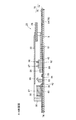
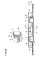
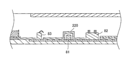
- FIG. 4 is a cross-sectional view taken along the line AA of the light emitting module of FIG. 3.
- FIG. 4 is a cross-sectional view taken along the line BB of the light emitting module of FIG. 3.
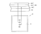
- It is a schematic diagram showing the correspondence of the panel side electric power feeding part and each layer of an organic EL element in the organic EL panel of FIG. It is the circuit diagram which simplified the electric circuit in the light emitting module of FIG.
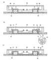
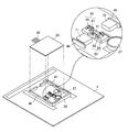
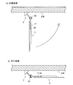
- FIG. 1 is a perspective view at the time of attaching a circuit board to a light emission panel. It is explanatory drawing of the attachment procedure of the light emitting module of FIG. 1, (a) is a side view showing the state attached in the crossing attitude
- the present invention relates to a light emitting module mounting structure 1 mainly used as a lighting device.
- a light emitting module mounting structure 1 mainly used as a lighting device.
- the positional relationship between the top, bottom, left, and right will be described based on the posture of FIG. 2 unless otherwise specified. That is, the light extraction side when the light emitting module 5 is lit is down.
- the physical properties described below represent the physical properties in the standard state unless otherwise noted, and the drawings are entirely in actual sizes (length, width, thickness) for easy understanding. It may be exaggerated in comparison.
- the light emitting module mounting structure 1 is a structure in which a light emitting module 5 is mounted on an installation target surface 200 such as a ceiling or a wall in parallel with a plurality of light emitting modules 5. It is.
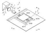
- the light emitting module mounting structure 1 is formed of a fixture 2 and a light emitting module 5 as shown in FIG.
- the fixture 2 is a member that is integrally fixed to the installation target surface 200 and attaches the connection tool 3 to the installation target surface 200.
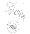
- the fixture 2 has a support portion 6 and a fixed-side fitting portion 7.
- the support part 6 is formed of a connection part 10 and a connection part 11.
- the connection part 10 is a site
- the connecting portion 10 is a triangular prism portion having a right triangle shape in cross section, and the triangular prism is inclined in the horizontal direction. That is, the slope 12 of the connection part 10 is the direction which cross
- the connecting portion 11 is formed of a shaft portion 21 and a ball portion 22.
- the shaft portion 21 is a portion that protrudes from the inclined surface 12 of the connecting portion 10 in the perpendicular direction, and is a cylindrical portion.
- the shaft portion 21 is connected to the ball portion 22 at the tip in the protruding direction from the inclined surface 12.
- the ball portion 22 is a portion that can be engaged with a ball receiving portion 15 of the fixed-side fitting portion 7 described later, and is a substantially spherical portion.
- the ball part 22 is a part that functions as a ball joint by being housed in the ball receiving part 15 of the fixed-side fitting part 7. That is, the ball portion 22 constitutes a free joint when the mounting structure 1 is assembled, and becomes the rotation center of the light emitting module 5.
- the fixed-side fitting portion 7 has a ball receiving portion 15, a fitting-side shaft portion 16, and a fitted portion 17.
- the ball receiving portion 15 is a portion that is paired with the ball portion 22 of the connecting portion 11, and is a portion having a storage space in which a part or all of the ball portion 22 can be stored.
- the ball receiving portion 15 is a portion whose inner surface is a concave spherical surface.
- the to-be-fitted part 17 is a site
- the fitted portion 17 is a box-like body opened in one direction, and has an insertion space 20 into which the connection fitting portion 28 can be inserted. That is, one end of the fitted portion 17 is an open end.
- the insertion space 20 of the fitted portion 17 has a fixed-side connection terminal 23 that is electrically connected to an external power source and an external device.
- the fixed connection terminal 23 is a power supply terminal that supplies power to the circuit board 25 (control board) shown in FIG. 5 from an external power source, and is also a signal input terminal that inputs a control signal from an external device to the circuit board 25.
- the fitted portion 17 includes a push-push type eject mechanism inside.
- this eject mechanism when the connection fitting portion 28 is pushed into the insertion space 20, the connection fitting portion 28 is locked, and when the connection fitting portion 28 is pushed again, the lock is released and the connection fitting portion is released.
- Reference numeral 28 denotes a mechanism capable of discharging from the insertion space 20.
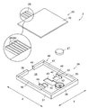
- the light emitting module 5 is formed of a connector 3 and a light emitting panel 4 as shown in FIG.
- the module mounting structure 1 of this embodiment has one of the characteristics in the electrical and physical connection relationship between the connector 3 and the light-emitting panel 4. Therefore, the structures of the connector 3 and the light emitting panel 4 will be described in more detail.
- the connection tool 3 includes a circuit board 25 (control board), a connection base 26, and a magnet part 27 (second adsorption part).
- the circuit board 25 is a printed circuit board (PCB) in which a connection side circuit 31 (see FIG. 13) described later is mounted on a plate-like or film-like circuit base material 30 (connection-side base material).
- the circuit board 25 is a single-sided board in which the connection side circuit 31 (see FIG. 13) is mainly mounted on one side of the plate-like circuit base material 30.
- the circuit substrate 30 is a substrate formed of epoxy resin, ceramics, or the like. The connection side circuit 31 of the circuit board 25 will be described in detail later.
- connection fitting portion 28 is a protruding piece that is integrally fixed to the circuit substrate 30 and protrudes in the surface direction from the end portion of the circuit substrate 30.
- the connecting fitting portion 28 can be fitted to the fitted portion 17 of the fixed-side fitting portion 7.
- the connection fitting portion 28 has a connection side connection terminal 29 (power feeding portion) that is electrically connected to the connection side circuit 31 (control circuit).
- the connection side connection terminal 29 is a terminal connected to the fixed side connection terminal 23 when the connection fitting portion 28 and the fitted portion 17 are fitted.
- connection side connection terminal 29 is a power supply terminal that receives power from the fixed side connection terminal 23 and supplies power to the connection side circuit 31, and inputs a control signal from the fixed side connection terminal 23 to the connection side circuit 31. It is also a signal input terminal.
- connection base 26 is a base on which the circuit board 25 can be placed as shown in FIG. 5, and is formed of an insulator.
- the method for forming the connection base 26 is not particularly limited, but is preferably formed by injection molding.
- the connection base 26 includes a base body 44, locking pieces 48 and 49 (engagement pieces), and a magnet storage unit 50.
- the base body 44 is a dish-like member, and has a substantially square bottom surface forming portion 35 and side surface forming portions 36, 37, 38, 39 rising from four sides of the bottom surface forming portion 35.
- the bottom surface forming portion 35 includes fitting through holes 40 and 41 (support holes), a control side through hole 42, and a power supply side through hole 43 (storage through hole), and these through holes 40, 41, Both 42 and 43 penetrate the bottom surface forming portion 35 in the thickness direction.
- the control side through hole 42 and the power supply side through hole 43 are formed adjacent to each other in the surface direction, and a part thereof is connected. That is, the control side through hole 42 and the power supply side through hole 43 form one through hole in the plane and are continuous in the surface direction of the bottom surface forming portion 35.
- fitting through holes 40 and 41 are connected to the control side through hole 42 and the power supply side in a direction intersecting the direction in which the control side through hole 42 and the power supply side through hole 43 are arranged in parallel (the orthogonal direction in the present embodiment). It is formed in the position which opposes on both sides of the through-hole 43.
- the control side through hole 42 is a through hole in which the second terminal 83 (see FIG. 5) can be accommodated.
- the control-side through hole 42 forms a power supply accommodating portion that can accommodate the second terminal 83.
- the power supply side through hole 43 is a through hole that can accommodate the adjusting element 81 and the first terminal 82 (see FIG. 5). That is, the power supply side through-hole 43 forms a control accommodating portion that can accommodate the adjusting element 81 and the first terminal 82.
- the side surface forming portion 36 has a cutout portion 45 into which the connection fitting portion 28 can be inserted.
- the cutout 45 is a cutout that is cut out from the end in the protruding direction of the side surface forming portion 36 toward the base end.
- the notch 45 is located at the center in the width direction Y of the side surface forming portion 36.
- the side surface forming portions 37 and 39 are partially cut off at the end in the protruding direction, and a step is formed on the end surface in the protruding direction. That is, the side surface forming portions 37 and 39 have recessed portions 46 and 47 that are recessed compared to other portions.
- the widths of the recesses 46 and 47 are substantially equal to the width of the circuit substrate 30 of the circuit board 25, and the recesses 46 and 47 fix the circuit substrate 30 of the circuit board 25. It is possible.
- the locking pieces 48 and 49 have a thin plate shape, and have hemispherical locking projections 51 and 52 (wall side engaging portions) on the side surfaces of the locking pieces 48 and 49. As shown in FIG. 7, the locking pieces 48 and 49 are partially disposed in the fitting through holes 40 and 41, and both end portions are fixed to the bottom surface forming portion 35. Specifically, the locking pieces 48 and 49 are integrally connected to a part of the bottom surface forming portion 35 and are supported at both ends so as to be in an upright posture by the connecting portion. From another viewpoint, the locking pieces 48 and 49 are formed so as to be divided across the fitting through holes 40 and 41 as shown in FIG. In other words, the locking pieces 48 and 49 are sandwiched between the slit-shaped grooves 53 and 54.
- the locking pieces 48 and 49 have a space in the thickness direction and have a degree of freedom of bending. Therefore, the locking pieces 48 and 49 can be elastically deformed toward the space.
- the locking pieces 48 and 49 protrude in the thickness direction with respect to the bottom surface forming portion 35, and locking protrusions 51 and 52 are formed in the vicinity of the end in the protruding direction.
- the magnet housing part 50 is a part into which the magnet part 27 can be inserted, and is a cylindrical part whose one side is closed by the bottom surface forming part 35 as shown in FIG. That is, the magnet storage unit 50 is surrounded by a cylindrical wall portion standing on the bottom surface forming portion 35, and can be said to be a bottomed hole having the bottom surface forming portion 35 as a bottom portion.
- the magnet unit 27 is a known permanent magnet and has a disk shape.
- the circuit board 25 is fixed to the connection base 26 as shown in FIG.
- the circuit substrate 30 is fixed to the recesses 46 and 47 so that the connection side circuit 31 (see FIG. 13) faces the bottom surface forming portion 35.
- One side of the circuit substrate 30 (the surface opposite to the connection side circuit 31) is flush with the protruding end portions of the side surface forming portions 37 and 39 as shown in FIG.
- the magnet part 27 is inserted into the magnet housing part 50.
- the light-emitting panel 4 includes a frame member 60 and an organic EL panel 61 (panel body).
- the frame member 60 is a member that functions as a frame of the organic EL panel 61 and is a member that fixes the organic EL panel 61 to the connector 3.
- the frame member 60 is formed of a frame main body 67, reinforcing members 62, 63, 64, a ferromagnetic body 65 (first adsorption portion), and a power supply substrate 66.
- the frame main body 67 is formed of a flexible resin, and is formed of a frame portion 70 and panel side protruding portions 71 and 72 (protruding portions) as shown in FIG.
- the frame portion 70 is a portion having a substantially “L” cross-sectional shape in the vicinity of the end portion, and is formed of an end face cover portion 74 and a back side cover portion 75. Yes. That is, the end surface cover 74 is erected from the peripheral end of the back surface cover 75.
- the end surface covering portion 74 is a portion that covers the peripheral end surface of the organic EL panel 61 when the light emitting panel 4 is assembled.
- the back surface covering portion 75 is a back surface of the organic EL panel 61 when the light emitting panel 4 is assembled. It is a part covering (the surface opposite to the light emitting surface 8).
- the back side cover 75 has a power supply insertion hole 95 (insertion hole) through which the first terminal 82 can be inserted and a control insertion hole 94 (insertion through which the second terminal 83 can be inserted. Insertion hole).
- the control insertion hole 94 is a through hole having an opening area substantially the same as that of the control side through hole 42 (see FIG. 7).
- the power supply insertion hole 95 is a through hole having an opening area substantially equal to that of the power supply side through hole 43 (see FIG. 7).
- the back side cover part 75 has panel side protrusion parts 71 and 72, a magnetic material storage part 76, and reinforcing member storage parts 77, 78, and 79, as can be read from FIGS.
- the panel side projecting portions 71 and 72 are projecting pieces that project from the back surface side covering portion 75.
- the panel-side protruding portions 71 and 72 are formed with locking grooves 92 and 93 (projecting-side engaging portions) on the outer side surfaces in the juxtaposed direction (vertical direction Y). ing. That is, the side surfaces on which the panel-side protrusions 71 and 72 are formed face in opposite directions.
- the locking grooves 92 and 93 are long grooves having a V-shaped cross section. That is, the inner surfaces of the locking grooves 92 and 93 are tapered so as to be inclined downward toward the center in the width direction of the locking grooves 92 and 93.
- the locking grooves 92 and 93 are formed so as to cross the side surfaces of the panel side protrusions 71 and 72, and extend in the lateral direction X.
- the magnetic material storage unit 76 is a part that can store the ferromagnetic material 65.
- the reinforcing member storage portions 77, 78, and 79 are portions that can store the reinforcing members 62, 63, and 64.
- the reinforcing members 62, 63, and 64 are reinforcing plates that reinforce the rigidity of the frame body 67, and are also reinforcing plates that reinforce the rigidity of the organic EL panel 61.
- the reinforcing members 62, 63, 64 are all long plate-shaped reinforcing plates.
- the material of the reinforcing member 62 is not particularly limited as long as it can reinforce the rigidity of the organic EL panel 61.
- a single metal such as aluminum, iron, nickel, cobalt, and gadolinium, a metal alloy, a metal Oxides and the like.
- the reinforcing member 62 of this embodiment is formed of an iron plate.
- the reinforcing members 62, 63, 64 are rectangular long plates and extend in a band shape.
- the ferromagnetic body 65 is a member having ferromagnetism and receiving a magnetic force from the magnet unit 27. Specifically, the ferromagnetic body 65 is a metal piece having ferromagnetism. The ferromagnetic material 65 of this embodiment employs an iron plate.
- the power supply board 66 is a thin plate-like or sheet-like printed board, and in the present embodiment, is a flexible printed board.
- the power supply substrate 66 is obtained by mounting an internal wiring such as a printed wiring (not shown) on a power supply base material 80.
- the power supply board 66 includes an adjustment element 81, a first terminal 82, and a second terminal 83 on one side of the power supply base member 80 as shown in FIG. 8, and the other surface as shown in FIG.
- a third terminal 84 is provided on the side.
- the adjustment element 81 is an element that can adjust the adjustment factor according to the characteristics of the organic EL element 100.
- the adjusting element 81 of the present embodiment is a resistor whose electric resistance value can be adjusted.
- the adjustment element 81 of the present embodiment is a semi-fixed resistor whose electric resistance value can be changed by an external element such as a driver.
- the first terminal 82 has a first power supply terminal 86 and a second power supply terminal 87 as shown in FIG.
- the first power supply terminal 86 and the second power supply terminal 87 are arranged in the horizontal direction X.
- the second terminal 83 has a first control terminal 88 and a second control terminal 89.
- the first control terminal 88 and the second control terminal 89 are arranged in a direction (vertical direction Y) orthogonal to the horizontal direction X.
- the third terminal 84 has a third feeding terminal 90 and a fourth feeding terminal 91 as shown in FIG.
- the panel side protrusions 71 and 72 of the frame member 60 are located on the main surface opposite to the light emitting surface 8 of the organic EL panel 61 as shown in FIG. That is, in the entire light emitting panel 4, the light emitting surface 8 is located on one main surface (light emitting side main surface) of the light emitting panel 4, and the panel side protrusions 71 and 72 are on the other main surface (back side main surface). positioned.
- the panel-side protruding portions 71 and 72, the magnetic material storage portion 76, the control insertion hole 94, and the power supply insertion hole 95 are all locally integrated within a predetermined range when the light-emitting panel 4 is viewed in plan view.
- the panel-side protruding portions 71 and 72, the magnetic material storage portion 76, the control insertion hole 94, and the power supply insertion hole 95 are centered on the center of the light emitting panel 4 when the light emitting panel 4 is viewed in plan view.
- the light emitting panel 4 is similar in area to the light emitting panel 4 and is all within an installation area that is an area that is half the area of the light emitting panel 4.
- the panel side protrusions 71 and 72, the magnetic material storage portion 76, the control insertion hole 94, and the power supply insertion hole 95 are 1 ⁇ 4 of the area of the light emitting panel 4. It is preferable to be within the installation area, and more preferably within the installation area that is 1/8 of the area of the light emitting panel 4.
- the frame member 60 is arranged in a row in the lateral direction X in the order of the feeding insertion hole 95, the control insertion hole 94, and the ferromagnetic body 65.
- the vertical direction Y (the direction orthogonal to the horizontal direction and also orthogonal to the thickness direction Z)
- Panel side protrusions 71 and 72 are located outside the feeding insertion hole 95, the control insertion hole 94, and the ferromagnetic body 65.
- Reinforcing members 62 and 63 are disposed on both outer sides in the vertical direction Y of the panel-side protruding portions 71 and 72, and the reinforcing member 64 is located on the outer side in the lateral direction X of the reinforcing members 62 and 63.
- the reinforcing members 62 and 63 both extend in the lateral direction X as shown in FIG.
- the reinforcing members 62 and 63 are arranged at a predetermined interval in the longitudinal direction Y, and are parallel to each other.
- the reinforcing member 64 extends in a direction crossing the extending direction of the reinforcing members 62 and 63, and the reinforcing member 64 extends in the vertical direction Y in this embodiment.
- the reinforcing member 64 is located on the outer side (end side) of the reinforcing members 62 and 63 in the lateral direction X.
- the reinforcing member 64 extends from the vicinity of one end in the vertical direction Y to the vicinity of the other end.
- the reinforcing members 62, 63, 64 are all laid on the same plane.
- the organic EL panel 61 is an organic EL panel in which an organic EL element 100 (light emitting element) is incorporated as shown in FIG. 12, and has a light emitting surface 8 on one main surface (one surface). That is, as shown in the upper diagram of FIG. 12, the organic EL panel 61 has a built-in laminated structure in which the organic EL elements 100 are laminated on a base material 101 having a planar shape.
- the organic EL element 100 has a laminated structure including at least a first electrode layer 102, an organic light emitting layer 103, and a second electrode layer 105 from the substrate 101 side.
- the organic EL panel 61 of the present embodiment is a bottom emission type organic EL panel that extracts light from the substrate 101 side.
- the organic EL panel 61 is a polygonal panel, and the organic EL panel 61 of this embodiment is a rectangular plate-like panel.
- the organic EL panel 61 has panel-side power feeding units 106 and 107 on the back surface (the surface opposite to the light emitting surface 8 side, the top surface). That is, in the organic EL panel 61, the base material 101 is located on the light emitting surface 8 side, and the second electrode layer 105 is located on the panel side power feeding units 106 and 107 side. As shown in FIG. 12, the panel-side power feeding unit 106 is electrically connected to the first electrode layer 102 of the organic EL element 100, and the panel-side power feeding unit 107 is connected to the second electrode layer 105 of the organic EL element 100. Electrically connected.
- a conductive path that connects the panel-side power supply unit 107 through the first electrode layer 102, the organic light emitting layer 103, and the second electrode layer 105 is formed from the panel-side power supply unit 106. Yes. Therefore, in the organic EL panel 61, when a voltage is applied between the panel-side power feeding units 106 and 107, the organic light emitting layer 103 emits light and the light emitting surface 8 emits light.
- FIG. 13 shows a simplified electrical circuit constructed by the light emitting module mounting structure 1 of the present embodiment.
- the light emitting module 5 is driven by receiving a current supplied from the external power source 210.
- the organic EL panel 61 includes an organic EL element 100.
- the power supply substrate 66 includes an adjustment element 81.
- the circuit board 25 mounts the connection side circuit 31 and mainly includes a sense resistor 114, a field effect transistor 115, a constant voltage diode 116, and an IC control unit 117.
- the sense resistor 114 is a known chip resistor and is extremely larger than a resistor that can be set by the adjustment element 81. Note that the sense resistor 114 may be a combined resistor of a plurality of resistors.
- the field effect transistor 115 is a field effect transistor having a drain, a gate, and a source, and is an N-channel MOSFET in this embodiment.
- the constant voltage diode 116 is a known Zener diode.
- the IC control unit 117 is a part capable of detecting a current and capable of transmitting a control signal to the field effect transistor 115.
- the external power source 210 is a DC power source, and in this embodiment, a DC stabilized power source is used.
- the external power source 210 is connected to the connection side connection terminal 29 of the connection tool 3 via the fixed side connection terminal 23 of the fixture 2.
- the connection side connection terminal 29 is connected to the first control terminal 88 of the power supply board 66 via the first circuit side path 110 (supply side power supply path) of the circuit board 25.
- the first control terminal 88 is connected to the adjustment element 81 via the internal wiring of the power supply board 66, and the adjustment element 81 is connected to the second control terminal 89 via the internal wiring of the power supply board 66. That is, the first control terminal 88 is electrically connected in series with the second control terminal 89 via the adjustment element 81.
- the second control terminal 89 is connected to the first power supply terminal 86 of the power supply board 66 via the second circuit side path 111 (circuit side power supply path) of the circuit board 25.
- the power supply board 66 is connected to a third power supply terminal 90 located on the opposite surface via an internal wiring.
- the third power supply terminal 90 is connected to the fourth power supply terminal 91 via the organic EL element 100, and the fourth power supply terminal 91 is located on the opposite surface via the internal wiring of the power supply substrate 66. It is connected to the dual power supply terminal 87.
- the second power supply terminal 87 is connected to the field effect transistor 115 via the third circuit side path 112 of the circuit board 25, and the field effect transistor 115 is connected to the connection side connection terminal 29 via the fourth circuit side path 113. It is connected.
- connection side connection terminal 29 is connected to the external power source 210 via the fixed side connection terminal 23 of the fixture 2.
- the light emitting module 5 forms the power feeding circuit 120 in which the adjustment element 81, the organic EL element 100, and the field effect transistor 115 are connected in series in this order from the external power source.
- the circuit board 25 also includes a first bypass path 118 (a bypass path) and a second bypass path 119 (a bypass path) that connect the first circuit side path 110 and the second circuit side path 111 so as to bypass the adjustment element 81.
- a sense resistor 114 is connected in the middle of the first bypass path 118
- an IC control unit 117 is connected in the middle of the second bypass path 119.
- the adjustment element 81, the sense resistor 114, and the IC control unit 117 are connected in parallel to each other, and the current between the first circuit side path 110 and the second circuit side path 111 is detected based on these relations.
- a current detection circuit is configured.
- the voltage between the first circuit side path 110 and the second circuit side path 111 is detected by the IC control unit 117, and the first circuit side path is determined from the combined resistance of the adjustment element 81 and the sense resistor 114.
- the current between 110 and the second circuit side path 111 is detected.
- the circuit board 25 has a connection circuit 121 that connects the first circuit side path 110 and the third circuit side path 112. In the middle of the connection circuit 121, a constant voltage diode 116 is connected. That is, the voltage between the first circuit side path 110 and the third circuit side path 112 is made constant by the constant voltage diode 116, and the current supplied to the organic EL element 100 is made constant. That is, the circuit board 25 includes a stabilization circuit that passes through the adjustment element 81, the sense resistor 114, the organic EL element 100, and the constant voltage diode 116, and the current that flows through the organic EL element 100 by this stabilization circuit. Is a constant current.
- the IC control unit 117 is connected to the external signal input unit 122 via the fixed-side connection terminal 23 and the connection-side connection terminal 29, and a control signal (external control) that performs PWM control, on / off control, and the like from the signal input unit 122. Signal). Further, the IC control unit 117 is connected to the gate of the field effect transistor 115 and can output a drive signal to the field effect transistor 115. That is, the light emitting module 5 outputs a drive signal to the field effect transistor 115 based on the control signal received from the signal input unit 122 by the IC control unit 117 and controls the field effect transistor 115. By doing so, the amount of power supplied to the organic EL element 100 is controlled, and the dimming of the organic EL element 100 is enabled.
- each member of the light emitting module mounting structure 1 will be described along the procedure for mounting the light emitting module 5 on the installation target surface 200.
- the power supply substrate 66 is connected to the organic EL panel 61 and then the frame member 60 is attached to form the light emitting panel 4.
- the back surface side cover 75 of the frame member 60 covers the surface opposite to the light emitting surface 8 of the organic EL panel 61
- the end surface cover 74 covers the end surface of the organic EL panel 61.
- the third power supply terminal 90 of the third terminal 84 of the power supply substrate 66 is in contact with the panel-side power supply unit 106 and is physically connected, and the fourth power supply terminal 91 is connected. It is physically connected in contact with the panel-side power feeding unit 107.
- the light emitting panel 4 is attached to the connection base 26 so as to be close thereto.
- the ferromagnetic body 65 is attracted by the magnetic force of the magnet portion 27 and is close to the connection tool 3.
- a bottom surface forming part 35 that forms the bottom part of the magnet housing part 50 is interposed. That is, the magnet part 27 and the ferromagnetic body 65 are attracted to each other by the magnetic force through the bottom surface forming part 35.
- the locking pieces 48 and 49 are pressed by the panel-side protrusions 71 and 72 and elastically deformed outward as shown in FIGS.
- control side through hole 42 and the control insertion hole 94 communicate with each other to form one communication hole, as can be seen from FIG. That is, a storage space in which the second terminal 83 can be stored is formed inside the communication hole.
- the second terminal 83 is connected to the circuit board 25 through a communication hole including the control side through hole 42 and the control insertion hole 94.
- the power supply side through hole 43 and the power supply insertion hole 95 communicate with each other to form one communication hole. That is, a storage space in which the first terminal 82 and the adjustment element 81 can be stored is formed inside the communication hole.
- the first terminal 82 is connected to the circuit board 25 through a communication hole including the power supply side through hole 43 and the power supply insertion hole 95.
- the circuit board 25 is attached to the recesses 46 and 47 and the circuit board 25 is fixed to form the light emitting module 5.
- the circuit board 25 is disposed so as to cover the first terminal 82, the second terminal 83, and the adjustment element 81 exposed from the connection base 26. That is, the circuit board 25 is arranged so that one side of the circuit substrate 30 faces the back surface of the light emitting panel 4. Further, most of the connection side circuit 31 of the circuit board 25 faces the back surface of the light emitting panel 4. Furthermore, the magnet part 27 is not covered with the circuit board 25 as shown in FIG. Therefore, the circuit board 25 is not easily affected by the magnetic force by the magnet unit 27.
- the light emitting module 5 is manufactured by performing the above steps.
- the light emitting module 5 manufactured in the above-described process is attached to the fixture 2.
- the fitting portion 17 of the fixture 2 is placed in a posture (crossing posture) that intersects the installation target surface 200, and the connection fitting portion 28 of the circuit board 25 is covered. It is inserted into the fitting part 17 and fixed.
- connection-side connection terminal 23 in the insertion space 20 of the fitted portion 17 is connected in contact with the connection-side connection terminal 29 of the connection fitting portion 28.
- the light emitting module 5 is lifted to the installation target surface 200 side with the ball portion 22 as the rotation center as shown by the arrow in FIG. 17A, and the posture parallel to the installation target surface 200 as shown in FIG. (Parallel posture).
- the fitted portion 17 of the fixture 2 When replacing with a new light emitting module 5, the fitted portion 17 of the fixture 2 is placed in a posture intersecting the installation target surface 200 with the ball portion 22 as the rotation center. Then, the connection fitting portion 28 of the circuit board 25 is pulled out and removed.
- connection fitting portion 28 of the newly prepared light emitting module 5 is fitted to the fitted portion 17, the light emitting module 5 is lifted to the installation target surface 200 side with the ball portion 22 as the rotation center, and the installation target surface The posture is parallel to 200.
- the device on the circuit base material 30 of the circuit board 25 is covered by the circuit base material 30 and the insulating connection base 26, so that the user can Touching conductive parts such as equipment and wiring can be prevented.
- the wedge effect works when the locking projections 51 and 52 are fitted into the locking grooves 92 and 93. Therefore, the locking projections 51 and 52 are firmly fitted in the locking grooves 92 and 93, and the integrated strength is high.
- the thickness of the adjustment element 81 is thicker than the normal fixed resistance. Therefore, a space for arranging the adjustment element 81 in the thickness direction protruding from the power supply base member 80 of the power supply substrate 66 is required. Therefore, in the light emitting module 5 of the present embodiment, a storage space in which the adjustment element 81 can be stored is formed by the power supply side through hole 43 of the connection base 26 and the power supply insertion hole 95 of the frame member 60. Therefore, the installation location of the adjustment element 81 can be secured, and the adjustment element 81 does not interfere with the attachment.
- the circuit board 25 of the fixture 2 and the connector 3 is electrically and mechanically connected by the fitting relationship between the fixed side fitting portion 7 and the connection fitting portion 28. Connected. In other words, the circuit board 25 of the fixture 2 and the connection tool 3 is electrically disconnected by releasing the fitting relationship between the fixed-side fitting part 7 and the connection fitting part 28.
- the circuit board 25 of the fixture 2 and the connection tool 3 is electrically disconnected by releasing the fitting relationship between the fixed-side fitting part 7 and the connection fitting part 28.
- the three members of the light emitting panel 4, the connecting tool 3, and the fixing tool 2 can be attached to and detached from each other.
- the members interlock to control the light emitting panel 4. Therefore, for example, when the light emitting panel 4 breaks down, the failed light emitting panel 4 can be used by replacing it with a new light emitting panel 4, and repairs such as failure are easy.
- the control method can be changed by replacing the connector 3.
- the fixing method can be changed by changing the fixing tool 2.
- the adjustment element 81 of the power supply board 66 is energized from the external power supply 210 via the circuit board 25, but the present invention is not limited to this, and the external power supply 210 is not limited to the circuit board 25.
- the power may be directly supplied to the adjustment element 81 of the power supply substrate 66 from the power supply board 66.
- the locking protrusions 51 and 52 are provided on the locking pieces 48 and 49 of the connection base 26, and the locking grooves 92 and 93 are formed in the panel side protrusions 71 and 72 of the frame member 60.
- the present invention is not limited to this, and the locking pieces 48 and 49 are provided with recesses, and the panel-side protrusions 71 and 72 are provided with protrusions. It may be engaged.
- connection fitting portion 28 that is a convex portion is provided on the circuit board 25 and is fitted to the fitted portion 17 that is the concave portion provided in the fixture 2.
- the circuit board 25 may be provided with a recess, and the fixture 2 may be provided with a protrusion to be fitted to each other.
- the connection fitting portion 28 is provided on the circuit board 25.
- the present invention is not limited to this, and the connection fitting portion 28 is provided on the connection base 26 as shown in FIG. May be provided.
- connection fitting portion 28 of the circuit board 25 and the fitting portion 17 of the fixture 2 is used for both the mechanical connection and the electrical connection.
- the connection relationship between the connection fitting portion 28 of the circuit board 25 and the fitted portion 17 of the fixture 2 may be used only for mechanical connection.
- the reinforcing members 62, 63, and 64 are arranged on the same plane.
- the present invention is not limited to this, and the reinforcing members 62, 63, and 64 are slightly displaced in the height direction. It may be. That is, the reinforcing members 62 and 63 and the reinforcing member 64 may be in a relationship extending in a direction intersecting with each other when projected onto the same plane.
- the present invention is not limited to this, and the mounting position of the light emitting module 5 is not limited.
- the connecting member 3 is provided with the magnet portion 27 and the light emitting panel 4 is provided with the ferromagnetic body 65.
- the present invention is not limited to this, and the connecting device 3 includes the ferromagnetic body 65.
- the magnet portion 27 may be provided on the light emitting panel 4.
- the adjustment element 81 is inserted and accommodated in the power supply side through hole 43 and is covered by the circuit base material 30 of the circuit board 25, thereby adjusting when the connection tool 3 is attached to the light emitting panel 4.
- the element 81 is made inoperable, the present invention is not limited to this.
- a storage recess 220 is provided in the connection base 26, and the adjustment element 81 is stored in the storage recess 220. By doing so, the adjustment element 81 may be made inoperable when the connector 3 is attached to the light emitting panel 4.
Landscapes
- Engineering & Computer Science (AREA)
- General Engineering & Computer Science (AREA)
- Microelectronics & Electronic Packaging (AREA)
- Physics & Mathematics (AREA)
- Optics & Photonics (AREA)
- Power Engineering (AREA)
- Electroluminescent Light Sources (AREA)
- Fastening Of Light Sources Or Lamp Holders (AREA)
- Arrangement Of Elements, Cooling, Sealing, Or The Like Of Lighting Devices (AREA)
Abstract
本発明は、製造において必然的に生じる有機ELパネルの個体差や異なる種類の有機ELパネル間での個体差を吸収できる発光モジュールを提供する。 接続具は、接続側回路を備えており、接続側回路は、発光パネルへの給電に寄与する回路側給電経路を有し、発光パネルは、調整素子と、発光素子を有し、調整素子は、電気抵抗値を調整できるものであり、調整素子は、回路側給電経路を介して発光素子と電気的に接続されている構成とする。
Description
本発明は、発光モジュールに関するものである。本発明は、特に照明用の有機ELパネルを内蔵した発光モジュールに関するものである。また、本発明は、その発光モジュールの一部を構成する接続具に関するものである。さらに、本発明は、発光モジュールを設置対象面に取り付ける発光モジュールの取付構造に関するものである。
近年、白熱灯や蛍光灯に代わる照明装置として、有機ELパネルを内蔵した有機ELモジュールが注目されている。
有機ELパネルは、一般的に、ガラス基板等の基材上に有機EL素子を積層し、有機EL素子を封止する構造及び有機EL素子へ給電する構造を備えたものである。
また、有機EL素子は、一方又は双方が透光性を有する2つの電極を対向させ、この電極の間に有機化合物からなる発光層を積層したものである。有機ELパネルは、電気的に励起された電子と正孔との再結合のエネルギーによって発光する。
有機ELパネルは、一般的に、ガラス基板等の基材上に有機EL素子を積層し、有機EL素子を封止する構造及び有機EL素子へ給電する構造を備えたものである。
また、有機EL素子は、一方又は双方が透光性を有する2つの電極を対向させ、この電極の間に有機化合物からなる発光層を積層したものである。有機ELパネルは、電気的に励起された電子と正孔との再結合のエネルギーによって発光する。
有機ELモジュールは、面発光の有機ELパネルを使用しており、平面光源である。そのため、複数の有機ELモジュールを天井等の設置対象面に敷設して一つの照明として使用することがある。
しかしながら、有機ELパネルは、上記したように電子と正孔の再結合のエネルギーを使用するから、電極間を通過する電流量で発光量が変化する。すなわち、有機ELパネルは、電極や発光層等の品質によって内部抵抗が異なるので、電極間に通過する電流量が異なり、発光量が異なる。そのため、同一の製造ラインで製造した場合であっても、品質に個体差が生じる場合がある。
この電気抵抗値の個体差による発光への影響は、微量なものであるが、有機ELモジュールを調光制御する場合には、精密な調光ができなくなる。また、複数枚の有機ELモジュールを平面状に敷設して使用する場合においては、隣接する有機ELモジュール間で濃淡が生じてしまう場合がある。
この電気抵抗値の個体差による発光への影響は、微量なものであるが、有機ELモジュールを調光制御する場合には、精密な調光ができなくなる。また、複数枚の有機ELモジュールを平面状に敷設して使用する場合においては、隣接する有機ELモジュール間で濃淡が生じてしまう場合がある。
また、開発実情において、製品は、日々改良されていくので、製造時期によっては、同一モデル又はその後継モデルの製品であっても製造方法が異なる場合がある。そのため、新旧製品間で若干の個体差が生じるおそれがある。
そこで、従来から有機ELパネルは、半固定抵抗を備えた制御基板を設けて、製品間の個体差を吸収する構造となっている。すなわち、半固定抵抗によって電気抵抗値を合わせて有機EL素子への給電量を調整し、できる限り製品間での内部抵抗の個体差をなくす試みがなされている。
ところで、このような有機ELパネルを用いた照明装置では、外部装置との電気的に接続したときの施工性を向上させ、その接続に伴って生じる配置の制約を減らすことが望まれている。
そこで、例えば、特許文献2では、光源部と、光源部の非発光面側に取り付けられる装着部を備え、前記装着部が、光源部を点灯制御する回路基板と、その回路基板と外部装置とを電気的に繋ぐための導線が接続される接続端子を有した照明装置が開示されている。この照明装置は、接続端子が装着部における光源部の取付け面の外周端部よりも内方寄りに配置されており、光源部に装着部が取り付けられた状態で、光源部と装着部との間に隙間が形成されるものである。そして、特許文献2では、この照明装置によれば、光源部と装着部の間に導線を収容するスペースが確保できるとしている。そのため、外部装置と電気的に接続する際に、配置に応じて導線を曲げるためのスペースが必要になる場合であっても、対応でき、施工性が向上するとしている。また、この照明装置では、導線を収容するスペースを確保するための配置制限をなくすこともできるとしている。
そこで、例えば、特許文献2では、光源部と、光源部の非発光面側に取り付けられる装着部を備え、前記装着部が、光源部を点灯制御する回路基板と、その回路基板と外部装置とを電気的に繋ぐための導線が接続される接続端子を有した照明装置が開示されている。この照明装置は、接続端子が装着部における光源部の取付け面の外周端部よりも内方寄りに配置されており、光源部に装着部が取り付けられた状態で、光源部と装着部との間に隙間が形成されるものである。そして、特許文献2では、この照明装置によれば、光源部と装着部の間に導線を収容するスペースが確保できるとしている。そのため、外部装置と電気的に接続する際に、配置に応じて導線を曲げるためのスペースが必要になる場合であっても、対応でき、施工性が向上するとしている。また、この照明装置では、導線を収容するスペースを確保するための配置制限をなくすこともできるとしている。
また、特許文献3には、上記したような発光モジュール間での個体差に基づく、光出力のばらつきを抑えるために、各発光モジュールに、それぞれの発光素子の特性を記憶した半導体メモリを設け、この半導体メモリから読み出した発光素子の特性に応じて、発光素子への供給電力を制御する方法が開示されている。
また、特許文献3には、発光素子に電力を供給する給電端子に対して抵抗素子を介して出力端子を接続し、出力端子の出力に基づいて、発光素子への供給電力をフィードバック制御する点灯装置が記載されている。そして、この点灯装置は、抵抗素子の一部を発光素子と同一基板上に薄膜状の抵抗体で形成し、その抵抗体の抵抗値をトリミングにより調整することによって、抵抗素子の抵抗値を個体差に合わせて予め調整することが可能となっている。
また、特許文献3には、発光素子に電力を供給する給電端子に対して抵抗素子を介して出力端子を接続し、出力端子の出力に基づいて、発光素子への供給電力をフィードバック制御する点灯装置が記載されている。そして、この点灯装置は、抵抗素子の一部を発光素子と同一基板上に薄膜状の抵抗体で形成し、その抵抗体の抵抗値をトリミングにより調整することによって、抵抗素子の抵抗値を個体差に合わせて予め調整することが可能となっている。
ところで、有機ELパネルを制御する制御基板は、調光等の制御にも使用される。この場合、調光等の制御方法によって制御基板の制御回路が異なる。
逆に言えば、制御方法が同じであれば、基本的には、制御基板は、同一の制御回路を備えることとなる。そのため、同様の制御を行う場合には、コスト面を抑える観点から、同じ制御基板を使用したいという要望がある。
逆に言えば、制御方法が同じであれば、基本的には、制御基板は、同一の制御回路を備えることとなる。そのため、同様の制御を行う場合には、コスト面を抑える観点から、同じ制御基板を使用したいという要望がある。
しかしながら、有機ELパネルの種類が異なると、想定される個体差が異なり、調整する抵抗の範囲が異なる。そのため、有機ELパネルの種類ごとに制御基板を製造する必要があった。それ故に、実装される制御基板の汎用性が低く、一の種類の有機ELパネルに合わせて形成された制御基板を他の種類の有機ELパネルに使用できないという問題が生じていた。
そこで、本発明は、製造において必然的に生じる有機ELパネルの個体差や異なる種類の有機ELパネル間での個体差を吸収できる発光モジュールを提供することを目的とする。また、その発光モジュールに用いられる有機ELパネルの接続具を提供することを目的とする。さらに、発光モジュールを天井等の設置対象面に取り付けるための発光モジュールの取付構造を提供することを目的とする。
本発明者は、上記した課題を解決するために、調光制御等を行う制御基板と、個体差を吸収するための調整素子を切り離して設けることによって、制御基板の汎用性を高めることを試みた。すなわち、内部抵抗の個体差吸収のための調整機構の一部を有機ELパネル側に持たせることで、制御基板の使い回しを可能とし、製造コストの削減を図った。そして、本発明者は、こうすることによって、1種類の制御基板で複数種類の有機ELパネルでも使用できると考察した。
上記した考察のもと導き出された本発明の一つの様相は、発光面を有する発光パネルと、前記発光パネルを設置対象面への固定具に接続するための接続具を備えた発光モジュールにおいて、前記接続具は、接続側回路を備えており、前記接続側回路は、前記発光パネルへの給電に寄与する回路側給電経路を有し、前記発光パネルは、調整素子と、発光素子を有し、前記調整素子は、前記発光素子の特性に応じて調整因子を調整できるものであり、前記調整素子は、前記回路側給電経路を介して前記発光素子と電気的に接続されている発光モジュールである。
ここでいう「設置対象面」とは、発光パネルを設置する対象となる被設置面を表し、具体的には、天井や壁面、床面、桟等である。
ここでいう「調整因子」とは、電気抵抗値や電圧値、電流値、電力量、熱量などの可変因子であり、発光素子への給電に寄与する因子である。
ここでいう「調整因子」とは、電気抵抗値や電圧値、電流値、電力量、熱量などの可変因子であり、発光素子への給電に寄与する因子である。
本様相によれば、発光素子の特性に応じて電気抵抗値等の調整因子を調整可能な調整素子を有するので、発光パネルの製造時等によって発光パネル間で生じる個体差を、調整素子によって調整することができる。そのため、発光パネル間で発光量を統一することが可能であり、調光等の制御を行う場合でも精密に調光することができる。
また本様相によれば、発光パネル側に調整素子を備えており、発光パネルの調整素子を用いて電気抵抗値等の調整因子の調整が可能である。このことから、接続具に個体差を吸収するための調整素子を設ける必要がなく、発光パネルの種類に合わせて接続具を形成しなくてもよい。そのため、本様相によれば、一の発光パネルに合わせて形成した接続具を他の発光パネルでも使用することが可能となり、製造コストを抑制することができる。
また本様相によれば、発光パネル側に調整素子を備えており、発光パネルの調整素子を用いて電気抵抗値等の調整因子の調整が可能である。このことから、接続具に個体差を吸収するための調整素子を設ける必要がなく、発光パネルの種類に合わせて接続具を形成しなくてもよい。そのため、本様相によれば、一の発光パネルに合わせて形成した接続具を他の発光パネルでも使用することが可能となり、製造コストを抑制することができる。
好ましい様相は、前記調整素子が自己の電気抵抗値を調整できることである。
本様相によれば、発光パネルの特性の調整が容易である。
好ましい様相は、前記接続側回路は、前記発光パネルへの給電に寄与する供給側給電経路をさらに有し、前記供給側給電経路は、前記調整素子を介して回路側給電経路と電気的に直列接続されており、前記調整素子は、前記回路側給電経路を介して前記発光素子と電気的に直列接続されていることである。
本様相によれば、電気抵抗値等の調整因子を調整可能な調整素子を有するので、発光パネルの製造時等によって発光パネル間で生じる個体差を調整素子によって調整することができる。そのため、発光パネル間で発光量を統一することが可能であり、調光等の制御を行う場合でも精密に調光することができる。
また本様相によれば、接続具の供給側給電経路から発光パネルの調整素子を経由して接続具の回路側給電経路に戻る経路が存在する。すなわち、接続具に設けられた接続側回路と発光パネルの調整素子を用いて1つの回路を形成し、調整素子により電気抵抗値等の調整因子の調整が可能であるから、接続具に個体差を吸収するための調整素子を設ける必要がなく、発光パネルの種類に合わせて接続具を形成しなくてもよい。そのため、一の発光パネルに合わせて形成した接続具を他の発光パネルでも使用することが可能となり、製造コストを抑制することができる。
また本様相によれば、接続具の供給側給電経路から発光パネルの調整素子を経由して接続具の回路側給電経路に戻る経路が存在する。すなわち、接続具に設けられた接続側回路と発光パネルの調整素子を用いて1つの回路を形成し、調整素子により電気抵抗値等の調整因子の調整が可能であるから、接続具に個体差を吸収するための調整素子を設ける必要がなく、発光パネルの種類に合わせて接続具を形成しなくてもよい。そのため、一の発光パネルに合わせて形成した接続具を他の発光パネルでも使用することが可能となり、製造コストを抑制することができる。
より好ましい様相は、前記接続側回路は、前記調整素子を迂回し、前記供給側給電経路と回路側給電経路を繋ぐ迂回路を有しており、前記調整素子は、供給側給電経路と回路側給電経路の間での電流を検知する電流検知回路の一部を構成することである。
本様相によれば、調整素子は、迂回路に対して電気的に並列接続されており、電流検知回路の一部を構成する。そのため、供給側給電経路と回路側給電経路の間での電流を電圧として検知でき、制御や調整素子の調整等が容易となる。
好ましい様相は、前記供給側給電経路及び回路側給電経路のうち少なくとも一方は、発光素子へ通電する電流を一定電流とするための安定化回路を構成することである。
本様相によれば、発光素子に安定した電流を流すことが可能であり、発光素子の発光にノイズ等の影響が生じにくい。
好ましい様相は、前記供給側給電経路及び回路側給電経路のうち少なくとも一方は、外部信号を受けて発光素子への給電量を制御する制御回路を構成することである。
本様相によれば、例えばPWM制御信号やオンオフ制御信号等の制御信号を外部から送信することで、発光パネルの調光制御が可能である。
好ましい様相は、前記接続具は、板状又はフィルム状の接続側基材に接続側回路を実装した回路基板を有し、前記接続側回路の大部分は、前記接続側基材の片面に実装されており、回路基板は、前記接続側基材の片面が発光パネルと対面するように配されていることである。
ここでいう「接続側回路の大部分が実装される」とは、配線を除く主要機器の4/5個以上の機器が実装されていることをいう。例えば、10個の主要機器がある場合には、8個以上の主要機器が実装されていることをいう。
本様相によれば、回路基板は、接続側基材の主に実装された面(以下、実装面ともいう)が発光パネルと対面するように配されている。言い換えると、接続側基材の実装面と反対側の面(以下、非実装面ともいう)が発光パネルに対して外側に位置する。すなわち、接続具を非実装面側からみたときに、発光パネルへの給電に寄与する接続側回路の大部分を接続側基材が被覆しているので、調整素子の調整作業などの際に、作業者が不意に接続側回路に触れてしまうことを防止でき、感電等の発生を防止できる。それ故に、本様相によれば、例えば、調整作業において、高い安全性が確保できる。
なお、上記した定義では、接続側基板の片面に「接続側回路の大部分が実装」されている状態を、接続側基板の片面に配線を除く主要機器の4/5以上の機器が実装されている状態としたが、より安全性が高い観点から、主要機器の全てが接続側基板の片面に実装されていることが好ましい。
なお、上記した定義では、接続側基板の片面に「接続側回路の大部分が実装」されている状態を、接続側基板の片面に配線を除く主要機器の4/5以上の機器が実装されている状態としたが、より安全性が高い観点から、主要機器の全てが接続側基板の片面に実装されていることが好ましい。
ところで、例えば、調整素子が、電気抵抗値を外部要素により調整可能な半固定抵抗で構成されている場合、調整素子が固定抵抗で構成されている場合に比べて、厚みが嵩張るおそれがある。
そこで、上記した問題を踏まえた好ましい様相は、前記接続具は、前記接続側回路を実装した回路基板と、当該回路基板を固定する接続台を備えており、前記接続台は、収納用凹部又は収納用貫通孔を有し、前記発光パネルに前記接続具を取り付けたときに、前記調整素子は、その一部が前記収納用凹部又は収納用貫通孔内に収納されていることである。
本様相によれば、例えば、半固定抵抗を調整素子として用いた場合であっても、調整素子の一部が接続台の前記収納用凹部又は収納用貫通孔内に収納されているので、調整素子の厚みによる発光モジュールの嵩張りを抑制することができる。
上記した問題を踏まえた好ましい別の様相は、前記発光パネルは、給電基板を有し、前記給電基板は、調整素子を実装しており、前記接続具は、前記接続側回路を実装した回路基板と、当該回路基板を固定する接続台を備えており、前記接続台は、制御側貫通孔を有し、前記発光パネルに前記接続具を取り付けたときに、前記調整素子は、その一部が前記制御側貫通孔内に収納されていることである。
本様相によれば、半固定抵抗を調整素子として用いた場合であっても、上記様相と同様、調整素子の厚みによる発光モジュールの嵩張りを抑制することができる。
なお、上記した制御側貫通孔は、上記した収納用貫通孔と同一であってもよい。
好ましい様相は、前記発光パネルは、給電基板を有し、前記給電基板は、前記調整素子と電気的に接続された制御端子と、前記発光素子と電気的に接続された給電端子を実装しており、前記接続具は、前記接続側回路を実装した回路基板と、当該回路基板を固定する接続台を備えており、前記接続台は、制御側貫通孔と、給電側貫通孔を有し、前記制御端子は、前記制御側貫通孔に挿入されて前記接続側回路と物理的に接続されており、前記給電端子は、前記給電側貫通孔に挿入されて前記接続側回路と物理的に接続されていることである。
本様相によれば、制御端子及び給電端子は、ともに接続台のそれぞれの貫通孔に挿入されて回路基板の接続側回路に物理的に接続されているので、発光モジュールを組み立てたときに、作業者が制御端子及び給電端子に触れることを防止することができる。また制御端子及び給電端子の一部又は全部がそれぞれの貫通孔に入っているため、制御端子及び給電端子の厚みによる発光モジュールの嵩張りを抑制することができる。
好ましい様相は、前記制御側貫通孔は、前記収納用貫通孔と部分的に繋がって、一つの貫通孔を形成していることである。
好ましい様相は、前記発光パネルは、前記発光面を有するパネル本体と、前記パネル本体の発光面に対して反対側の面を覆うフレーム部材を有し、前記フレーム部材は、前記発光面に対して交差する方向に突出した突出部を有し、前記突出部は、その側面に突出側係合部が形成されており、前記接続具は、接続台を備えており、前記接続台は、支持孔を有した台本体と、前記支持孔の開口に沿って台本体に対して立設された係合片を有しており、前記係合片は、その側面に壁側係合部が形成されており、前記発光パネルを接続具に取り付ける際に、前記突出部を前記支持孔に挿入させて、前記突出側係合部を前記壁側係合部に係合させることである。
本様相によれば、発光パネルを接続具に取り付ける際に、突出部を支持孔に挿入させて、突出側係合部と壁側係合部を互いに係合させる。そのため、発光パネルと接続具の一方を他方に対して相対的に移動させることによって、発光パネルと接続具を一体化させることができる。すなわち、本様相によれば、一つの移動動作で容易に発光パネルと接続具を一体化させることができる。
より好ましい様相は、前記係合片は、薄板であって、その一部又は全部が前記支持孔の内部に位置し、さらに前記係合片は、前記支持孔を分割するように前記台本体に支持されており、前記発光パネルを前記接続具に取り付ける際に、前記係合片は、前記突出部によって押圧されて弾性変形し、その復元力が前記突出部に向かって生じていることである。
本様相によれば、発光パネルを接続具に取り付ける際に、接続台の係合片は、フレーム部材の突出部によって押圧されて弾性変形し、その復元力が突出部に向かって生じている。そのため、突出部の突出側係合部と係合片の壁側係合部が互いに近接する方向に付勢されて、より係合関係が強固なものとなる。それ故に、接続具と発光パネルが互いに離反しにくく、一体化強度が高い。
好ましい様相は、前記発光パネルは、前記発光面を有するパネル本体と、前記パネル本体の発光面に対して反対側の面を覆うフレーム部材を有し、前記フレーム部材は、前記発光面に対して交差する方向に突出した突出部を少なくとも2つ有し、前記2つの突出部は、その側面に突出側係合部が形成されており、前記接続具は、接続台を備えており、前記接続台は、台本体と、少なくとも2つの係合片を有しており、前記台本体は、支持孔を少なくとも2つ有し、前記2つの係合片は、前記支持孔に対応して配されるものであって、対応する開口に沿って、台本体に対して立設されており、前記2つの係合片は、薄板状であって、互いに対面し、さらに当該対面する面に前記壁側係合部が形成されており、前記2つの突出部は、対応する支持孔に挿入しており、前記突出側係合部は、対応する壁側係合部と係合していることである。
本様相によれば、2つの突出片が対応する2つの支持孔に挿入されているので、発光面の面方向において、発光パネルが接続具に対してずれにくい。
さらに、本様相によれば、係合片は、他の係合片と対面する面に壁側係合部が形成されており、当該壁側係合部と突出部の側面に形成された突出側係合部が係合する。すなわち、2つの係合片の内側に2つの係合片が位置し、内外の位置関係によって壁側係合部と突出側係合部が係合する。つまり、2つの突出片を外側から2つの係合片が挟むことによって発光パネルと接続具が固定されている。そのため、2つの突出片の並ぶ方向において、発光パネルが接続具に対してずれにくく、発光パネルが接続具に対して離反しにくい。また、たとえ天井等に設置した場合でも壁側係合部と突出側係合部の係合関係によって、発光パネルが係止されるので、落下しない。
さらに、本様相によれば、係合片は、他の係合片と対面する面に壁側係合部が形成されており、当該壁側係合部と突出部の側面に形成された突出側係合部が係合する。すなわち、2つの係合片の内側に2つの係合片が位置し、内外の位置関係によって壁側係合部と突出側係合部が係合する。つまり、2つの突出片を外側から2つの係合片が挟むことによって発光パネルと接続具が固定されている。そのため、2つの突出片の並ぶ方向において、発光パネルが接続具に対してずれにくく、発光パネルが接続具に対して離反しにくい。また、たとえ天井等に設置した場合でも壁側係合部と突出側係合部の係合関係によって、発光パネルが係止されるので、落下しない。
より好ましい様相は、前記発光パネルは、給電基板を有し、前記給電基板は、前記調整素子と電気的に接続された制御端子と、前記発光素子と電気的に接続された給電端子を実装しており、前記接続具は、前記接続側回路を実装した回路基板と、当該回路基板を固定する接続台を備えており、前記接続台は、制御側貫通孔と、給電側貫通孔を有し、前記制御端子は、前記制御側貫通孔に挿入されて前記接続側回路に物理的に接続されており、前記給電端子は、前記給電側貫通孔に挿入されて前記接続側回路と物理的に接続されており、前記突出部、制御側貫通孔及び給電側貫通孔は、発光パネルを平面視したときに、発光パネルの中央を中心とした発光パネルと相似形状の領域であって、かつ、発光パネルの面積の1/2の面積となる領域である設置領域内にいずれも収まっていることである。
本様相によれば、突出部、制御側貫通孔及び給電側貫通孔は、発光パネルの面積の1/2の面積となる領域である設置領域内に収まっている。そのため、対応する支持孔を有した接続台を必要以上に大きくせずとも、最低限の発光パネルの固定及び発光パネルへの給電が確保できる。すなわち、接続台の小型化が可能であり、接続台の材料コストを低減することができる。
より好ましい様相は、前記発光パネルは、前記発光面を有するパネル本体と、前記パネル本体の発光面に対して反対側の面を覆うフレーム部材と、給電基板を有し、前記フレーム部材は、前記発光面に対して交差する方向に突出した突出部を少なくとも2つ有し、前記給電基板は、前記調整素子と電気的に接続された制御端子と、前記発光素子と電気的に接続された給電端子を実装しており、前記接続具は、前記接続側回路を実装した回路基板と、当該回路基板を固定する接続台を備えており、前記接続台は、制御側貫通孔と、給電側貫通孔を有し、前記制御端子は、前記制御側貫通孔に挿入されて前記接続側回路に物理的に接続されており、前記給電端子は、前記給電側貫通孔に挿入されて前記接続側回路と物理的に接続されており、前記接続台は、絶縁体によって形成されるものであって、かつ、その一部が前記フレーム部材と前記回路基板の間に介在しており、前記制御側貫通孔及び前記給電側貫通孔は、前記2つの突出部の間に位置していることである。
本様相によれば、制御側貫通孔及び給電側貫通孔は、2つの突出部の間に位置している。そのため、外部から回路基板が押圧された場合でも、突出部が回路基板を当接することで回路基板を支持し、回路基板に実装された機器や調光素子が破損することを防止することができる。
好ましい様相は、前記発光パネルは、前記発光面を有するパネル本体と、前記パネル本体の発光面に対して反対側の面を覆うフレーム部材を有し、前記フレーム部材は、可撓性樹脂によって形成されたフレーム本体と、前記フレーム本体の剛性を補強する補強部材を備えることである。
本様相によれば、フレーム本体が可撓性樹脂によって形成されているので、パネル本体に取り付け易い。また、フレーム本体が可撓性樹脂によって形成されることによるフレームとしての剛性不足を補強部材によって補強することができる。そのため、本様相によれば、組み立てやすく十分な強度を有した発光モジュールとなる。
さらに本様相によれば、フレーム本体が可撓性樹脂によって形成されているので、パネル本体を接続具に取り付け易く、発光パネルの重量を軽くすることができる。
さらに本様相によれば、フレーム本体が可撓性樹脂によって形成されているので、パネル本体を接続具に取り付け易く、発光パネルの重量を軽くすることができる。
上記した様相は、前記フレーム本体は、補強部材収納部を有し、前記補強部材収納部は、少なくとも一方向に延びており、前記補強部材は、前記補強部材収納部に収納されていてもよい。
より好ましい様相は、前記フレーム部材は、前記補強部材を複数有し、前記補強部材は、長板状であり、前記複数の補強部材のうち少なくとも2枚の補強部材は、互いに平行に設置されており、前記調整素子の一部は、当該2つの補強部材の間に位置していることである。
本様相によれば、2つの補強部材の間に調整素子が位置しているので、落下等による衝撃から調整素子を保護することができる。
より好ましい様相は、前記フレーム部材は、前記補強部材を複数有し、前記補強部材は、板状であり、前記複数の補強部材のうち少なくとも2枚の補強部材は、同一平面に投影したときに、互いに交差する方向に延設されていることである。
本様相によれば、補強部材を同一平面に投影したときに、2枚の補強部材は、互いに交差する方向に延設されている。すなわち、これら2枚の補強部材により、前記平面における互いに直交する2方向成分を補強されるので、ねじれ等に対する発光パネルの剛性が高く、破損しにくい。
好ましい様相は、前記発光パネルは、前記接続台に対して着脱可能であることである。
本様相によれば、例えば、発光パネルが初期不良や損傷等によって機能しなくなり、修理が必要となったときに、当該発光パネルを新たな発光パネルに交換して接続具に取り付けることによって、修理対応が可能である。すなわち、本様相によれば、修理等の場合において、接続具を使い回すことができ、修理費用を抑えることができる。
好ましい様相は、前記発光パネルは、前記発光面を有するパネル本体と、前記パネル本体の発光面に対して反対側の面を覆うフレーム部材を有し、前記フレーム部材は、第一吸着部を有し、前記接続具は、第二吸着部を有し、前記第一吸着部と前記第二吸着部の間で発生する磁力によって、前記発光パネルが前記接続具に取り付けられることである。
本様相によれば、第一吸着部と第二吸着部の間で発生する磁力によって、発光パネルが接続具に取り付けられるので、発光パネルと接続具を近接させることによって、簡単に発光パネルと接続具を一体化させることが可能である。
また、本様相によれば、第一吸着部と第二吸着部の間で発生する磁力によって、発光パネルと接続具が引き寄せられるので、例えば、天井等に固定される場合であっても、発光パネルが接続具から落下しにくい。
また、本様相によれば、第一吸着部と第二吸着部の間で発生する磁力によって、発光パネルと接続具が引き寄せられるので、例えば、天井等に固定される場合であっても、発光パネルが接続具から落下しにくい。
上記した様相において、第一吸着部と第二吸着部のうち、一方の吸着部が磁石であり、他方の吸着部が強磁性体であってもよい。
上記した様相において、前記接続台は、台本体を有し、前記台本体は、前記第一吸着部と前記第二吸着部の間に介在していてもよい。
この様相によれば、接続具から発光パネルを着脱する際に第二吸着部が接続台から外れにくい。
好ましい様相は、前記調整素子は、半固定抵抗であることである。
本様相によれば、調整素子自身の電気抵抗値をドライバー等の外部要素によって調整することが可能である。すなわち、固定抵抗のように別途電気抵抗値の調整用の回路や制御が必要なく、個々の発光素子に合わせて調整しやすい。
好ましい様相は、前記発光素子は、2つの電極層と、当該2つの電極層に挟まれた有機発光層を備えた有機EL素子であることである。
本様相によれば、発光パネルは、有機ELパネルであるので、薄くて軽い発光モジュールにできる。
ところで、特許文献2に開示されている照明装置では、光源部と装着部との間に隙間が形成されている。このため、特許文献2の照明装置では、照明装置の施工者や使用者が、この隙間に露出している電気回路等に指等を接触させてしまい、電気回路等に不具合を生じさせる可能性がある。また特許文献2の照明装置では、誤って外部から給電されている状態で指等を接触させた場合に感電してしまうおそれが生じうる。そのため、特許文献2の照明装置は、安全性や信頼性に問題があり、改善の余地がある。
また、特許文献2の照明装置では、光源部と装着部とが係合により脱着可能であり、光源部と装着部を互いに係合して装着する際に、両者の係合部分と両者間で給電するための端子の結合部分とが同一面内にある。そのため、このような電気回路等が外部に露出する隙間が生じ易いと考えられる。
また、特許文献2の照明装置では、光源部と装着部とが係合により脱着可能であり、光源部と装着部を互いに係合して装着する際に、両者の係合部分と両者間で給電するための端子の結合部分とが同一面内にある。そのため、このような電気回路等が外部に露出する隙間が生じ易いと考えられる。
そこで、本発明者は、発光パネルと、当該発光パネルを脱着可能な接続具を備える発光モジュールであって、接続具から発光パネルを取り外した際に、接続具の回路や給電端子が外部に露出しない発光モジュールを提供するべく、以下の考察を行った。
すなわち、本発明者は、発光パネルと接続具との、機械的な係合部分と、電気的な結合部分とを、別面内に分離することによって、配線等を這わす隙間を保持しつつ、回路等への指等の接触を回避することを試みた。
具体的には、接続具の一部又は全部を接続台と回路基板によって構成し、発光パネルを脱着可能とする。そして、接続台に、発光パネルとの機械的係合機能と、その発光パネル側の面に回路露出防止機能とを併せ持たせる。さらに、回路基板に、発光パネルとの電気的結合機能と、その発光パネル側の面に回路露出防止機能とを併せ持たせる。これらにより、点灯制御する回路や外部装置と電気的に繋ぐための導線が接続される接続端子等(以下、単に接続端子等ともいう)を配置する隙間を保持しつつ、回路等が当該隙間に露出しないようにでき、指等の回路等への接触を防止できると考察した。
具体的には、接続具の一部又は全部を接続台と回路基板によって構成し、発光パネルを脱着可能とする。そして、接続台に、発光パネルとの機械的係合機能と、その発光パネル側の面に回路露出防止機能とを併せ持たせる。さらに、回路基板に、発光パネルとの電気的結合機能と、その発光パネル側の面に回路露出防止機能とを併せ持たせる。これらにより、点灯制御する回路や外部装置と電気的に繋ぐための導線が接続される接続端子等(以下、単に接続端子等ともいう)を配置する隙間を保持しつつ、回路等が当該隙間に露出しないようにでき、指等の回路等への接触を防止できると考察した。
この考察に基づいた本発明の一つの様相は、発光面を有する発光パネルと、前記発光パネルを設置対象面への固定具に接続するための接続具を備えた発光モジュールであって、前記発光パネルが前記接続具に対して着脱可能な発光モジュールにおいて、前記発光パネルは、発光素子と、当該発光素子と電気的に接続された給電端子を有しており、前記接続具は、板状又はフィルム状の接続側基材に接続側回路を実装した回路基板と、当該回路基板を固定する接続台とを有し、前記接続側回路は、前記発光パネルへの給電に寄与するものであって、その大部分が前記接続側基材の片面に実装されており、前記接続台は、少なくとも一部に絶縁体で形成された部分が存在し、当該絶縁体で形成された部分に給電側貫通孔を有するものであり、前記発光パネルを前記接続具に取り付けたときに、前記接続側基材の片面と前記発光パネルが対面し、前記発光パネルと前記回路基板の間に前記絶縁体で形成された部分が介在しており、さらに前記給電端子が前記給電側貫通孔に挿入されて前記接続側回路と物理的に接続されている発光モジュールである。
また、この考察に基づいた本発明の他の様相としては、発光面を有する発光パネルと、前記発光パネルを設置対象面への固定具に接続するための接続具を備えた発光モジュールにおいて、前記発光パネルは、発光素子と、該発光素子と電気的に接続された給電端子を有しており、前記接続具は、板状又はフィルム状の接続側基材に接続側回路を実装した回路基板と、当該回路基板を固定する接続台とを有し、前記接続側回路は、前記発光パネルへの給電に寄与する回路側給電経路を有し、前記接続側回路の大部分は、前記接続側基材の片面に実装されており、前記接続台は、絶縁体によって形成されるものであって、前記発光パネルと前記回路基板の間に介在しており、かつ、給電側貫通孔を有し、回路基板は、該片面が発光パネルと対面するように配されており、前記発光パネルは、前記接続台に対して着脱可能であり、前記発光パネルの前記接続具への装着時に、前記給電端子は、前記給電側貫通孔を挿通して前記接続側回路と物理的に接続される発光モジュールでもよい。
ここで、発光モジュールを制作するにあたって、発光パネルに対して脱着可能な接続具であって、汎用性・安全性に優れ、安価な接続具が必要とされている。
上記した様相によれば、発光パネルを脱着可能な接続具を備え、接続端子等を配置可能な隙間を保持しつつ、かつ、指等の接触が防止できるように回路等が露出しない。すなわち、上記した様相によれば、発光パネルと接続具との機械的な係合部分と、発光パネルと接続具との電気的な結合部分とを別面内に分離している。こうすることによって、回路設置や外部配線用の隙間を保持しつつ、回路部への指の接触を防止することができる。また、上記した様相によれば、接続具を外した状態でも感電可能性部位が露出しない。
このように本様相によれば、発光パネルに対して脱着可能な接続具であって、汎用性・安全性に優れ、安価な接続具を備えた発光モジュールとできる。
上記した様相によれば、発光パネルを脱着可能な接続具を備え、接続端子等を配置可能な隙間を保持しつつ、かつ、指等の接触が防止できるように回路等が露出しない。すなわち、上記した様相によれば、発光パネルと接続具との機械的な係合部分と、発光パネルと接続具との電気的な結合部分とを別面内に分離している。こうすることによって、回路設置や外部配線用の隙間を保持しつつ、回路部への指の接触を防止することができる。また、上記した様相によれば、接続具を外した状態でも感電可能性部位が露出しない。
このように本様相によれば、発光パネルに対して脱着可能な接続具であって、汎用性・安全性に優れ、安価な接続具を備えた発光モジュールとできる。
好ましい様相は、前記発光パネルは、前記発光面に対して交差する方向に突出した突出部を有し、前記突出部は、その側面に突出側係合部が形成されており、前記接続具は、接続台を備えており、前記接続台は、台本体と、係合片を有しており、前記台本体は、当該台本体の底面を構成する底面形成部を有し、前記底面形成部は、給電側貫通孔及び支持孔を有しており、前記係合片は、前記台本体に対して前記支持孔の開口に沿って立設されたものであって、かつ、その側面に壁側係合部が形成されており、前記発光パネルを接続具に取り付けたときに、前記突出部が前記支持孔に挿入されて、前記突出側係合部が前記壁側係合部と係合していることである。
好ましい様相は、前記発光パネルは、前記発光面に対して交差する方向に突出した突出部を有し、前記突出部は、その側面に突出側係合部が形成されており、前記接続台は、前記給電側貫通孔、及び支持孔を有する底面形成部を有した台本体と、前記支持孔の開口に沿って台本体に対して立設された係合片を有しており、前記係合片は、その側面に壁側係合部が形成されており、前記発光パネルを接続具に取り付ける際に、前記突出部を前記支持孔に挿通させて、前記突出側係合部を前記壁側係合部に係合させることである。
上記した様相によれば、接続台への発光パネルの着脱の信頼性が向上する。
好ましい様相は、前記接続具は、回路基板を有し、前記台本体は、皿状であって、前記底面形成部から立ち上がった側面形成部を有し、前記側面形成部には、前記立ち上がり方向の一部が切り欠かれて段差が形成されており、前記段差に前記回路基板を固定されていることである。
すなわち、上記した様相は、前記台本体は、皿状の部材であり、前記底面形成部と、該底面形成部から立ち上がった側面形成部を有し、該側面形成部には、前記回路基板を固定可能な凹部を形成するように、前記立ち上がり方向の一部が切り欠かれた段差形状が形成されていることが好ましい。
この様相によれば、台本体の存在によって、回路等の遮蔽機能が向上すると共に、発光モジュールの厚みを薄くできる。またこの様相によれば、接続具の機械的強度を向上し、発光モジュール全体の機械的強度も向上できる。
好ましい様相は、前記接続側基板の片面と前記底面形成部の間隔が、0.5mm以上、15mm以下であることである。
この範囲であれば、接続側基板と底面形成部の間に配線等を這わすことができる隙間を形成しつつ、誤って指が挿入されることを防止できる。
好ましい様相は、接続側基板と底面形成部の間隔が10mm以下であり、より好ましい様相は5mm以下である。
また、好ましい様相は、接続側基板と底面形成部の間隔が1mm以上であり、より好ましい様相は、2mm以上である。
また、好ましい様相は、接続側基板と底面形成部の間隔が1mm以上であり、より好ましい様相は、2mm以上である。
ところで、特許文献2に開示されている照明装置では、装着部の一端の被係合部に、光源部が傾けられた状態でその係合部が差し込まれた後、この係合部位を軸として光源部を回動させる。このようにして、光源部の他端の端子部、及び係合部が、装着部の端子溝部、及び被係合部に係合、及び結合される。また、装着部が予め装着対象に固定されている。それらのため、照明装置の全体の厚み等が装着部の厚み等によって実質的に決まってしまい、有機EL発光パネルの平面、薄い、軽いといった特徴を十分に生かすことができないという問題があり、改善の余地がある。
そこで、本発明者は、有機EL発光パネルを設置対象面の固定具に接続する接続具を備える発光モジュールにおいて、有機EL発光パネルの特徴を活かした、小さく、軽く、かつ、高信頼性の接続具を備える発光モジュールを提供するべく、以下の考察を行った。
すなわち、本発明者は、有機EL発光パネルと接続具を脱着可能に組み立て、有機EL発光パネルの中央又はその付近から、嵌合用の突出部、及び給電用の給電端子を外側に突出させて、接続具に接続することを試みた。つまり、嵌合用の突出部で発光パネルから突出した給電端子を保護しつつ、それらを発光パネルの中央付近の限られた範囲に設ける。そして、接続具に外部の電源側に突出し、発光パネルの嵌合用の突出部に適合する接続用の嵌合部を設ける。こうすることによって、小さく、軽く、高信頼性、高安全性、かつ、高汎用性の接続具にすることができ、有機EL発光パネルの特徴を損なわれにくい発光モジュールとなると考察した。
この考察に基づいた本発明の一つの様相は、発光パネルと、前記発光パネルを設置対象面への固定具に接続するための接続具を備えた発光モジュールであって、前記発光パネルは、発光面を有するパネル本体と、給電基板と、フレーム部材を有し、前記パネル本体は、少なくとも有機発光層を含んだ発光素子を有し、前記給電基板は、前記発光素子と電気的に接続された給電端子を実装しており、前記フレーム部材は、前記パネル本体の発光面に対して反対側の面を覆うフレーム本体を備え、前記フレーム本体は、前記発光面に対して交差する方向に突出した突出部を少なくとも2つ有し、前記2つの突出部は、側面に突出側係合部がそれぞれ形成されており、前記接続具は、接続台と、接続側回路を実装した回路基板を備えており、前記接続台は、当該回路基板を固定するものであって、台本体と、少なくとも2つの係合片を有しており、前記台本体は、給電側貫通孔と、少なくとも2つの支持孔を有し、前記2つの係合片は、前記2つの支持孔の各々に対応して配されるものであって、対応する開口に沿って、前記台本体に対して立設されており、さらに前記2つの係合片は、薄板状であって、互いに対面しており、その面内には壁側係合部が形成されており、前記2つの突出部、及び給電側貫通孔は、前記発光パネルを平面視したときに、前記発光パネルの中央を中心とした前記発光パネルと相似形状の領域であって、かつ、前記発光パネルの面積の1/2の面積となる領域である設置領域内に収まっており、前記発光パネルは、前記接続台に対して着脱可能であり、前記発光パネルを前記接続具に取り付けたときに、前記2つの突出部がそれぞれ対応する前記支持孔内に挿入されて、前記突出側係合部がそれぞれ前記壁側係合部と係合しており、前記給電端子は、前記2つの突出部の間に位置し、前記給電側貫通孔に挿入されて前記接続側回路と物理的に接続されていることを特徴とする発光モジュールである。
また、この考察に基づいた本発明の他の様相としては、発光面を有する発光パネルと、前記発光パネルを設置対象面への固定具に接続するための接続具を備えた発光モジュールにおいて、前記発光パネルは、前記発光面を有するパネル本体と、給電基板と、前記パネル本体の発光面に対して反対側の面を覆うフレーム部材を有し、前記発光パネル本体は、発光素子を有し、前記発光素子は、2つの電極層と、当該2つの電極層に挟まれた有機発光層を備えた有機EL素子であり、前記給電基板は、前記発光素子と電気的に接続された給電端子を実装しており、前記フレーム部材は、樹脂によって形成されたフレーム本体を備え、前記フレーム本体は、前記発光面に対して交差する方向に突出した突出部を少なくとも2つ有し、前記2つの突出部は、その側面に突出側係合部が形成されており、前記接続具は、接続台と、接続側回路を実装した回路基板を備えており、前記接続台は、当該回路基板を固定するものであり、台本体と、少なくとも2つの係合片を有しており、前記台本体は、給電側貫通孔と、少なくとも2つの支持孔を有し、前記2つの係合片は、前記支持孔の各々に対応して配されるものであって、対応する開口に沿って、台本体に対して立設されており、かつ、薄板状であって、互いに対面し、さらにその面内に壁側係合部が形成されており、前記2つの突出部、及び給電側貫通孔は、発光パネルを平面視したときに、発光パネルの中央を中心とした発光パネルと相似形状の領域であって、かつ、発光パネルの面積の1/2の面積となる領域である設置領域内に収まっており、前記発光パネルを接続具に取り付ける際に、前記突出部は、対応する前記支持孔に挿通させられ、前記突出側係合部は、対応する前記壁側係合部に係合させられ、かつ、前記給電端子は、前記給電側貫通孔を挿通して前記接続側回路と物理的に接続されることで、前記発光パネルは、前記接続台に対して着脱可能であり、前記給電端子は、前記2つの突出部の間に位置している発光モジュールでもよい。
上記した様相によれば、接続具を備えつつ、有機EL発光パネルの特徴を活かした、小さく、軽く、かつ、高信頼性の発光モジュールを提供することができる。
好ましい様相は、前記接続具は、前記発光パネルを平面視したときに、発光パネルの中央を中心とした前記発光パネルと相似形状の領域であって、かつ、発光パネルの面積の1/2の面積となる領域である設置領域内に収まっていることである。
より好ましい様相は、前記設置領域が発光パネルの面積の1/4の面積となる領域であることであり、さらに好ましい様相は、前記設置領域が1/8の面積となる領域であることである。
好ましい様相は、前記フレーム部材は、前記フレーム本体の剛性を補強する補強部材を少なくとも2枚備えており、前記2枚の補強部材は、長板状であって、平面視したときに互いに平行となるように離間しており、前記設置領域は、前記2枚の補強部材の間に位置していることである。
すなわち、前記フレーム部材は、前記フレーム本体の剛性を補強する複数の補強部材を備え、前記複数の補強部材のうち少なくとも2枚の補強部材は、互いに平行に、かつ、離間して設置された長板状の補強部材であり、前記設置領域は、当該2つの長板状の補強部材の間に位置していることが好ましい。
本様相によれば、設置領域内の給電端子は、接続具と、フレーム部材、特に突出部とに囲まれ、さらに、2つの補強部材の間に位置しているので、落下等による衝撃から調整素子を保護することができ、かつ、モジュール全体に十分な機械的強度を付与可能となる。
好ましい様相は、記発光パネルは、発光面を有するパネル本体と、給電基板と、前記パネル本体の発光面に対して反対側の面を覆うフレーム部材を有し、前記接続具は、回路基板と、当該回路基板を固定する接続台を備えており、前記接続台は、少なくとも一部に絶縁体で形成された部分が存在し、当該絶縁体で形成された部分は、前記フレーム部材と前記回路基板の間に介在していることである。
好ましい様相は、前記接続台は、絶縁体によって形成されるものであって、かつ、その一部が前記フレーム部材と前記回路基板の間に介在していることである。
より好ましい様相は、前記接続台は、前記発光パネル側の面内に調整素子格納用の凹部又は貫通孔を有し、前記調整素子は、その一部が前記調整素子格納用の凹部又は貫通孔内に収納されることである。
本様相によれば、例えば、調整素子として半固定抵抗を用いた場合であっても、調整素子の一部が接続台の調整素子格納用の凹部又は貫通孔内に収納されているので、調整素子の厚みによる発光モジュールの嵩張りを抑制することができる。
ところで、特許文献3に開示されている方法では、例えば、発光素子の特性を記憶した半導体メモリを用いる場合、発光モジュールを点灯させるためには、半導体メモリに発光素子の特性を記憶させる必要があるだけでなく、前記特性を読み出すことができ、且つ読み出した特性に応じて供給電力を制御することができる専用の点灯装置が必要になる。そのため、点灯装置の構成が複雑になるという問題がある。
また、発光素子が形成されたのと同一基板上の薄膜状の抵抗体をトリミングする方法を用いる場合、特性を安定化させるために、抵抗体をトリミングした後に、発光素子や抵抗体を封止したり、フレーミングしたりする必要がある。そのため、これら工程で特性変化や不良が発生する可能性があり、更なる改善の余地がある。
また、発光素子が形成されたのと同一基板上の薄膜状の抵抗体をトリミングする方法を用いる場合、特性を安定化させるために、抵抗体をトリミングした後に、発光素子や抵抗体を封止したり、フレーミングしたりする必要がある。そのため、これら工程で特性変化や不良が発生する可能性があり、更なる改善の余地がある。
そこで、本発明者は、有機EL発光パネルを設置対象面の固定具に接続する接続具を備える発光モジュールについて、(1)封止工程等を経て前記パネルを構成するフレーム部材を取り付けた状態で、供給電力をフィードバック制御するための調整素子を発光素子の特性に応じて調整できること、(2)前記接続具を構成する接続台を発光パネルに取り付けた状態で、前記発光素子と電気的に接続された給電端子、及び前記調整素子と電気的に接続された制御端子が、各々外部に露出し、むき出しとなっていること、の2点を満たす発光モジュールを提供するべく、以下の考察を行った。
すなわち、本発明者は、調整素子と、調整素子と電気的に接続された制御端子と、給電端子を給電基板の一部として実装する。そして、給電基板を発光パネルの主要部分であるパネル本体の発光面と反対側の面に載置し、フレーム部材を取り付けた状態で、調整素子の調整を可能とする。さらに、フレーム部材を取り付けることで給電端子をパネル本体の発光素子に電気的に接続可能とすることを試みた。
具体的には、調整に関係する部分である、調整素子及び制御端子を給電基板の一部として独立して設ける。この調整素子によって、発光パネル側で発光素子の特性に応じて調整因子を調整可能とする。また、接続具の発光パネルへ装着動作を行うことにより、この制御端子を接続具の一部である接続側回路に物理的・機械的に接続可能とする。このように調整素子と制御端子を分離して設けることによって、製品・品種間の特性差を吸収可能な、高信頼性、高生産性を備えた発光モジュールが提供できると考察した。また、発光モジュールとして完成品の状態で発光素子特性を記録可能であり、外部電力供給側に対して給電時の電圧印可部位が凸部位となって感電を防止可能な発光モジュールが提供できると考察した。
具体的には、調整に関係する部分である、調整素子及び制御端子を給電基板の一部として独立して設ける。この調整素子によって、発光パネル側で発光素子の特性に応じて調整因子を調整可能とする。また、接続具の発光パネルへ装着動作を行うことにより、この制御端子を接続具の一部である接続側回路に物理的・機械的に接続可能とする。このように調整素子と制御端子を分離して設けることによって、製品・品種間の特性差を吸収可能な、高信頼性、高生産性を備えた発光モジュールが提供できると考察した。また、発光モジュールとして完成品の状態で発光素子特性を記録可能であり、外部電力供給側に対して給電時の電圧印可部位が凸部位となって感電を防止可能な発光モジュールが提供できると考察した。
この考察に基づいた本発明の一つの様相は、発光パネルと、前記発光パネルを設置対象面への固定具に接続するための接続具を備えた発光モジュールにおいて、前記発光パネルは、発光面を有するパネル本体と、給電基板と、前記パネル本体の発光面に対して反対側の面を覆うフレーム部材を有し、前記パネル本体は、発光素子を有し、前記給電基板は、前記発光素子の特性に応じて調整因子を調整可能な調整素子と、前記調整素子と電気的に接続された制御端子と、前記発光素子と電気的に接続された給電端子を実装しており、前記フレーム部材は、挿入孔を有し、前記接続具は、回路基板と、当該回路基板を固定する接続台を備えており、前記接続台は、制御側貫通孔と、給電側貫通孔を有し、前記発光パネルから前記接続具を取り外した状態において、前記調整素子は調整可能なように外部に露出しており、前記発光パネルに前記接続台を取り付けた状態において、前記制御端子は、前記挿入孔と前記制御側貫通孔に挿入されて外部に露出しており、さらに前記給電端子は、前記挿入孔と前記給電側貫通孔に挿入されて外部に露出している発光モジュールである。
また、この考察に基づいた本発明の他の様相としては、発光面を有する発光パネルと、前記発光パネルを設置対象面への固定具に接続するための接続具を備えた発光モジュールにおいて、前記発光パネルは、調整素子を実装した給電基板と、発光素子と、前記発光面を有するパネル本体と、前記パネル本体の発光面に対して反対側の面を覆うフレーム部材を有し、前記調整素子は、前記発光素子の特性に応じて調整可能なものであり、前記給電基板は、さらに、前記調整素子と電気的に接続された制御端子と、前記発光素子と電気的に接続された給電端子を実装しており、前記フレーム部材は、挿通孔を有し、前記接続具は、接続側回路を実装した回路基板と、当該回路基板を固定する接続台を備えており、前記接続台は、制御側貫通孔と、給電側貫通孔と、調整素子格納用の凹部又は貫通孔を有し、前記発光パネルから前記接続具を取り外した状態で、前記調整素子は調整可能なようにむき出しとなるようにされてなり、かつ、前記発光パネルに前記接続台を取り付けた状態で、前記制御端子は前記挿通孔と前記制御側貫通孔を介して、前記給電端子は前記挿通孔と前記給電側貫通孔を介して、各々、前記接続側回路と物理的に接続可能なようにむき出しとなるようにされている発光モジュールでもよい。
上記した様相によれば、パネル本体にフレーム部材を取り付けた状態で、調整素子を調整できる。また、接続具を構成する接続台を発光パネルに取り付けた状態で、給電端子及び制御端子のそれぞれが外部に露出したむき出し状態とすることができる。そのため、給電端子及び制御端子への端子の接続が容易となり、発光モジュールを組み立てたときに、調整素子を介した外部からの発光素子への給電が容易となる。
好ましい様相は、前記調整素子格納用の凹部又は貫通孔は、前記接続台の前記発光パネル側の面内に存在することである。より好ましい様相は、前記調整素子は、その一部が前記調整素子格納用の凹部又は貫通孔内に収納されることである。
好ましい様相は、前記発光パネルに前記接続台を取り付けた状態において、前記調整素子が調整できないように前記調整素子格納用の凹部に覆われていることである。
好ましい様相は、前記発光パネルは、調整素子を有し、前記調整素子は、前記発光素子の特性に応じて調整因子を調整できるものであり、前記接続具は、接続台を備えており、前記接続台は、前記調整素子を格納可能な収納用凹部を有し、前記発光パネルに前記接続台を取り付けた状態において、前記調整素子は、前記収納用凹部によって調整できないように覆われていることである。
本様相によれば、例えば半固定抵抗等の調整素子は、接続台で覆われて隠された状態となる。そのため、誤って、発光パネルに装着した状態で、接続具を接続台と回路基板とに分離した場合にも、発光パネルに属する発光素子の特性の記録である調整素子の情報、例えば、調整値である抵抗値を、意図せずに変更してしまうことを防止できる。また、この情報の書き換えである修正は、発光パネルから接続具を取り外した状態で、発光パネルに対しての修正であることを認識した上で、実施されることとなる。
好ましい様相は、前記接続側回路は、前記発光パネルへの給電に寄与する回路側給電経路を有し、前記調整素子は、前記回路側給電経路を介して前記発光素子と電気的に接続されていることである。
この様相によれば、パネル本体に属する発光素子の特性情報を、非給電時にパネル本体と無関係にパネル本体の外部に取り出すことが可能である。
本発明の一つの様相は、発光面を有する発光パネルを設置対象面への固定具に接続可能な接続具であって、調整素子及び発光素子を有した前記発光パネルに接続可能な接続具において、前記調整素子は、前記発光素子の特性に応じて調整因子を調整できるものであり、前記発光パネルへの給電に寄与する回路側給電経路を有し、前記発光パネルと接続したときに、前記調整素子は、前記回路側給電経路を介して前記発光素子と電気的に接続されることを特徴とする接続具である。
本様相によれば、個体差を吸収する調整素子を備える発光パネルに使用されるものである。そのため、調整素子を内蔵しなくてもよいので、様々な発光パネルに使用できる。例えば、一の発光パネルに合わせて形成した場合であっても、同一の制御等を行う他の発光パネルでも使用することが可能となる。
本発明の一つの様相は、発光面を有する発光パネルを設置対象面への固定具に接続可能な接続具であって、前記発光パネルを着脱可能な接続具において、前記発光パネルは、少なくとも有機発光層を含んだ発光素子と、給電基板と、少なくとも2つの突出部を有し、当該2つの突出部が前記発光面に対して交差する方向に突出したものであって、突出部の側面に突出側係合部が形成されたものであり、さらに前記発光パネルは、前記給電基板が前記発光素子と電気的に接続された給電端子を実装したものであり、接続台と、接続側回路を実装した回路基板を備え、前記接続台は、前記回路基板を固定する台本体と、少なくとも2つの係合片を有しており、前記台本体は、給電側貫通孔と、少なくとも2つの支持孔を有し、前記2つの係合片は、前記支持孔の各々の開口に沿って、前記台本体に対して立設されており、かつ、板状であって、互いに対面し、さらにその面内に壁側係合部が形成されており、前記発光パネルを取り付けた状態を平面視したときに、前記2つの突出部が前記発光パネルの中央を中心とした前記発光パネルと相似形状の領域であって、かつ、前記発光パネルの面積の1/2の面積となる領域である設置領域内にいずれも収まっており、前記2つの支持孔に対応する2つの突出部のそれぞれが挿入されて、前記係合片の前記壁側係合部に発光パネルの突出側係合部が係合され、前記給電側貫通孔に前記給電端子が挿入されて、前記接続側回路が前記給電端子と物理的に接続された状態となって、全体が前記設置領域内に収まっている接続具である。
本発明の一つの様相は、発光面を有する発光パネルを設置対象面への固定具に接続可能な接続具であって、前記発光パネルは、発光素子と、前記発光面に対して交差する方向に突出した突出部を少なくとも2つ有し、前記発光素子は、2つの電極層と、当該2つの電極層に挟まれた有機発光層を備えた有機EL素子であり、前記2つの突出部は、その側面に突出側係合部が形成されており、前記接続具は、接続台と、接続側回路を実装した回路基板を備えており、前記接続台は、当該回路基板を固定するものであり、台本体と、少なくとも2つの係合片を有しており、前記台本体は、給電側貫通孔と、少なくとも2つの支持孔を有し、前記2つの係合片は、前記支持孔の各々に対応して配されるものであって、対応する開口に沿って、台本体に対して立設されており、かつ、板状であって、互いに対面し、さらにその面内に壁側係合部が形成されており前記2つの突出部、及び給電側貫通孔は、発光パネルを平面視したときに、発光パネルの中央を中心とした発光パネルと相似形状の領域であって、かつ、発光パネルの面積の1/2の面積となる領域である設置領域内にいずれも収まっており、前記発光パネルを接続具に取り付ける際に、前記突出部は、対応する前記支持孔に挿通させられ、前記突出側係合部は、対応する前記壁側係合部に係合させられ、かつ、前記給電端子は、前記給電側貫通孔を挿通して前記接続側回路と物理的に接続されることで、前記発光パネルは、前記接続台に対して着脱可能であり、かつ、前記接続具は、前記平面視したときに、前記設置領域内に収まっている接続具である。
上記した様相によれば、有機EL発光パネルの特徴を活かしつつ、小さく、軽く、かつ、高信頼性の接続具となる。
好ましい様相は、外部電源側に突出する接続用嵌合部を備えることである。
本様相によれば、外部電源側からの電力供給により生じる感電の危険を低減することができる。
本発明の一つの様相は、上記した様相の発光モジュールと、固定具を用いた発光モジュールの取付構造であって、前記発光パネルは、前記接続具によって、着脱可能に固定されており、前記接続具は、接続用嵌合部を有し、前記固定具は、設置対象面に対して一体的に固定されるものであって、かつ、固定側嵌合部を有し、前記固定側嵌合部と前記接続用嵌合部は、互いに着脱可能に嵌合している発光モジュールの取付構造である。
本様相によれば、固定側嵌合部と接続用嵌合部が互いに着脱可能に嵌合しているので、使用済み発光モジュールを新品の発光モジュールに交換して使用することができる。また、例えば、調整素子を備えた発光パネルを用いる場合には、交換時における製品間の個体差が調整素子によって吸収できるため、再現性よく発光パネルを発光させることができる。
好ましい様相は、前記接続用嵌合部が外部の電源側に突出することである。
本様相によれば、外部の電源側からの電力供給により生じる感電の危険を低減することができる。
本発明に関連する様相は、発光面を有する発光パネルと、前記発光パネルを設置対象面への固定具に接続するための接続具を備えた発光モジュールにおいて、前記接続具は、前記発光パネルへの給電に寄与する回路基板と、前記回路基板を支持する接続台を有し、前記回路基板は、外部電源と電気的に接続可能な給電部を有し、前記接続台は、接続側貫通孔を有し、前記発光パネルは、調整素子と、発光素子を有し、前記調整素子は、前記給電部から前記発光素子への給電経路の一部を形成し、前記発光素子への給電量を調整可能であり、接続具に発光パネルを取り付ける際には、前記接続台は、前記発光パネルに載置され、前記調整素子は、前記接続台の接続側貫通孔を挿通して回路基板と接続される発光モジュールである。
この様相によれば、調整素子の一部は、接続台の接続側貫通孔内に収納されているので、接続台の厚み分の調整素子の設置スペースを確保することができ、調整素子による嵩張りを低減することができる。
本発明に関連する様相は、発光面を有する発光パネルと、設置対象面と固定される固定具と、前記発光パネルを前記固定具に接続するための接続具を備えた発光モジュールの取付構造において、前記固定具は、制御信号を出力可能な固定側信号出力部を有し、前記接続具は、発光パネルへの給電量を制御する制御基板を有し、前記接続具は、前記固定具に対して着脱可能に取り付けられており、前記発光パネルは、前記接続具に対して着脱可能に取り付けられており、前記制御基板は、前記固定側信号出力部から出力された制御信号を入力して前記発光パネルの給電量を調整する発光モジュールの取付構造である。
この様相の構成によれば、発光パネルと接続具と固定具の3部材が互いに着脱可能となっており、発光パネルと接続具と固定具の3部材が連動して発光パネルを制御するものである。この構成によれば、例えば、発光パネルが故障した場合には、発光パネルを新たな発光パネルに交換して使用することが可能であり、発光パネルの制御方法を変更したい場合には、接続具を交換することで制御方法を変更することができる。また、固定具の設置対象面への固定方法を変更したい場合には、固定具を変更することで固定方法を変更することができる。
このように、この様相によれば、部品を分解して部品ごとに交換することによって、様々なニーズに応えることができる。
このように、この様相によれば、部品を分解して部品ごとに交換することによって、様々なニーズに応えることができる。
本発明の発光モジュールによれば、製造において必然的に生じる有機ELパネルの個体差や異なる種類の有機ELパネル間での個体差を吸収できる。
本発明の接続具によれば、異なる有機ELパネルでも調光等の制御が可能である。
本発明の発光モジュールの取付構造であれば、設置対象面への有機ELモジュールの取付が容易である。
本発明の接続具によれば、異なる有機ELパネルでも調光等の制御が可能である。
本発明の発光モジュールの取付構造であれば、設置対象面への有機ELモジュールの取付が容易である。
本発明は、主に照明装置として使用される発光モジュールの取付構造1に係るものである。以下、上下左右の位置関係は、特に断りのない限り、図2の姿勢を基準に説明する。すなわち、発光モジュール5の点灯時における光取り出し側が下である。また、下記に記載する物性は、特に断りの無い限り、標準状態での物性を表し、図面は、理解を容易にするために全体的に実際の大きさ(長さ、幅、厚さ)に比べて誇張して描写していることがある。
本発明の第1実施形態の発光モジュールの取付構造1は、図1に示されるように、複数の発光モジュール5と並列させて、天井や壁等の設置対象面200に発光モジュール5を取り付けるものである。
発光モジュールの取付構造1は、図2のように、固定具2と、発光モジュール5から形成されている。
固定具2は、図1のように、設置対象面200に一体的に固定され、設置対象面200に対して接続具3を取り付ける部材である。
固定具2は、図4に示されるように、支持部6と、固定側嵌合部7を有している。
固定具2は、図1のように、設置対象面200に一体的に固定され、設置対象面200に対して接続具3を取り付ける部材である。
固定具2は、図4に示されるように、支持部6と、固定側嵌合部7を有している。
支持部6は、図4のように、接続部10と、連結部11から形成されている。
接続部10は、図1,図2から読み取れるように、設置対象面200と連結部11を接続する部位である。
接続部10は、断面形状が直角三角形状の三角柱状の部位であり、三角柱が水平方向に傾倒した姿勢となっている。すなわち、接続部10の斜面12は、図1,図4から読み取れるように、設置対象面200に対して交差する方向であって、下方側を向いている。
接続部10は、図1,図2から読み取れるように、設置対象面200と連結部11を接続する部位である。
接続部10は、断面形状が直角三角形状の三角柱状の部位であり、三角柱が水平方向に傾倒した姿勢となっている。すなわち、接続部10の斜面12は、図1,図4から読み取れるように、設置対象面200に対して交差する方向であって、下方側を向いている。
連結部11は、図4に示されるように、軸部21と、ボール部22から形成されている。
軸部21は、接続部10の斜面12から垂線方向に突出した部位であり、円柱状の部位である。軸部21は、斜面12からの突出方向先端でボール部22が接続されている。
ボール部22は、後述する固定側嵌合部7のボール受け部15と係合可能な部位であり、略球状の部位である。また、ボール部22は、固定側嵌合部7のボール受け部15内に収納されることによってボールジョイントとして機能する部位である。すなわち、ボール部22は、取付構造1を組み立てた際に、自由継ぎ手を構成し、発光モジュール5の回動中心となる。
軸部21は、接続部10の斜面12から垂線方向に突出した部位であり、円柱状の部位である。軸部21は、斜面12からの突出方向先端でボール部22が接続されている。
ボール部22は、後述する固定側嵌合部7のボール受け部15と係合可能な部位であり、略球状の部位である。また、ボール部22は、固定側嵌合部7のボール受け部15内に収納されることによってボールジョイントとして機能する部位である。すなわち、ボール部22は、取付構造1を組み立てた際に、自由継ぎ手を構成し、発光モジュール5の回動中心となる。
固定側嵌合部7は、図4のように、ボール受け部15と、嵌合側軸部16と、被嵌合部17を有している。
ボール受け部15は、連結部11のボール部22と対をなす部位であり、ボール部22の一部又は全部を収納可能な収納空間を有した部位である。ボール受け部15は、内側面が凹球面状の部位である。
ボール受け部15は、連結部11のボール部22と対をなす部位であり、ボール部22の一部又は全部を収納可能な収納空間を有した部位である。ボール受け部15は、内側面が凹球面状の部位である。
被嵌合部17は、図2,図3から読み取れるように、発光モジュール5の接続用嵌合部28と嵌合可能な部位である。
被嵌合部17は、図4のように、一方方向に開放した箱状体であり、その内部に接続用嵌合部28を挿入可能な挿入空間20を有している。すなわち、被嵌合部17は、一方の端部が開放端となっている。
また、被嵌合部17の挿入空間20には、外部電源及び外部装置と電気的に接続された固定側接続端子23を有している。固定側接続端子23は、外部電源から図5に示される回路基板25(制御基板)に給電する給電端子であり、回路基板25に外部装置からの制御信号を入力する信号入力端子でもある。
被嵌合部17は、図4のように、一方方向に開放した箱状体であり、その内部に接続用嵌合部28を挿入可能な挿入空間20を有している。すなわち、被嵌合部17は、一方の端部が開放端となっている。
また、被嵌合部17の挿入空間20には、外部電源及び外部装置と電気的に接続された固定側接続端子23を有している。固定側接続端子23は、外部電源から図5に示される回路基板25(制御基板)に給電する給電端子であり、回路基板25に外部装置からの制御信号を入力する信号入力端子でもある。
被嵌合部17は、その内部にプッシュ・プッシュ式のイジェクト機構を備えている。
このイジェクト機構は、接続用嵌合部28を挿入空間20に押し込むと接続用嵌合部28がロックされ、接続用嵌合部28を再度押込むと、ロックが解除されて接続用嵌合部28が挿入空間20から排出できる機構である。
このイジェクト機構は、接続用嵌合部28を挿入空間20に押し込むと接続用嵌合部28がロックされ、接続用嵌合部28を再度押込むと、ロックが解除されて接続用嵌合部28が挿入空間20から排出できる機構である。
発光モジュール5は、図5に示されるように、接続具3と、発光パネル4によって形成されている。
そして、本実施形態のモジュールの取付構造1は、接続具3と、発光パネル4の電気的及び物理的な接続関係に特徴の一つを有している。そこで、接続具3と発光パネル4の構造についてさらに詳細に説明する。
接続具3は、図6に示されるように、回路基板25(制御基板)と、接続台26と、磁石部27(第二吸着部)を有している。
回路基板25は、板状又はフィルム状の回路用基材30(接続側基材)に後述する接続側回路31(図13参照)が実装されたプリント基板(PCB)である。
本実施形態では、回路基板25は、板状の回路用基材30の片面に主に接続側回路31(図13参照)が実装された片面基板である。
回路用基材30は、エポキシ樹脂やセラミックス等によって形成された基材である。
なお、回路基板25の接続側回路31については後に詳細に説明する。
回路基板25は、板状又はフィルム状の回路用基材30(接続側基材)に後述する接続側回路31(図13参照)が実装されたプリント基板(PCB)である。
本実施形態では、回路基板25は、板状の回路用基材30の片面に主に接続側回路31(図13参照)が実装された片面基板である。
回路用基材30は、エポキシ樹脂やセラミックス等によって形成された基材である。
なお、回路基板25の接続側回路31については後に詳細に説明する。
また、回路基板25は、図6に示されるように、接続用嵌合部28を有している。
接続用嵌合部28は、回路用基材30に対して一体的に固定され、回路用基材30の端部から面方向に突出した突出片である。接続用嵌合部28は、固定側嵌合部7の被嵌合部17と嵌合可能となっている。
接続用嵌合部28は、接続側回路31(制御回路)と電気的に接続された接続側接続端子29(給電部)を有している。
接続側接続端子29は、接続用嵌合部28と被嵌合部17を嵌合させたときに、固定側接続端子23と接続される端子である。すなわち、接続側接続端子29は、固定側接続端子23から電気の供給を受けて接続側回路31に給電する給電端子であり、接続側回路31に固定側接続端子23からの制御信号を入力する信号入力端子でもある。
接続用嵌合部28は、回路用基材30に対して一体的に固定され、回路用基材30の端部から面方向に突出した突出片である。接続用嵌合部28は、固定側嵌合部7の被嵌合部17と嵌合可能となっている。
接続用嵌合部28は、接続側回路31(制御回路)と電気的に接続された接続側接続端子29(給電部)を有している。
接続側接続端子29は、接続用嵌合部28と被嵌合部17を嵌合させたときに、固定側接続端子23と接続される端子である。すなわち、接続側接続端子29は、固定側接続端子23から電気の供給を受けて接続側回路31に給電する給電端子であり、接続側回路31に固定側接続端子23からの制御信号を入力する信号入力端子でもある。
接続台26は、図5のように回路基板25を載置可能な台座であり、絶縁体で形成されている。接続台26の形成方法は、特に限定されないが、射出成形によって形成されることが好ましい。
接続台26は、図6のように、台本体44と、係止片48,49(係合片)と、磁石収納部50を備えている。
接続台26は、図6のように、台本体44と、係止片48,49(係合片)と、磁石収納部50を備えている。
台本体44は、皿状の部材であり、略四角形状の底面形成部35と、底面形成部35の4辺から立ち上がった側面形成部36,37,38,39を有している。
底面形成部35は、嵌合用貫通孔40,41(支持孔)と、制御側貫通孔42と、給電側貫通孔43(収納用貫通孔)を備えており、これらの貫通孔40,41,42,43は、いずれも底面形成部35を厚み方向に貫通している。
制御側貫通孔42と給電側貫通孔43は、面方向に互いに隣接して形成されており、一部が繋がっている。すなわち、制御側貫通孔42と給電側貫通孔43は、面内に一つの貫通孔を形成しており、底面形成部35の面方向に連続している。
また、嵌合用貫通孔40,41は、制御側貫通孔42と給電側貫通孔43の並設方向に対して交差する方向(本実施形態では直交方向)において、制御側貫通孔42と給電側貫通孔43を挟んで対向する位置に形成されている。
底面形成部35は、嵌合用貫通孔40,41(支持孔)と、制御側貫通孔42と、給電側貫通孔43(収納用貫通孔)を備えており、これらの貫通孔40,41,42,43は、いずれも底面形成部35を厚み方向に貫通している。
制御側貫通孔42と給電側貫通孔43は、面方向に互いに隣接して形成されており、一部が繋がっている。すなわち、制御側貫通孔42と給電側貫通孔43は、面内に一つの貫通孔を形成しており、底面形成部35の面方向に連続している。
また、嵌合用貫通孔40,41は、制御側貫通孔42と給電側貫通孔43の並設方向に対して交差する方向(本実施形態では直交方向)において、制御側貫通孔42と給電側貫通孔43を挟んで対向する位置に形成されている。
制御側貫通孔42は、その内部に第二端子83(図5参照)を収納可能な貫通孔である。すなわち、制御側貫通孔42は、第二端子83を収納可能な給電用収容部を形成している。
給電側貫通孔43は、調整素子81及び第一端子82(図5参照)を収納可能な貫通孔である。すなわち、給電側貫通孔43は、調整素子81及び第一端子82を収納可能な制御用収容部を形成している。
給電側貫通孔43は、調整素子81及び第一端子82(図5参照)を収納可能な貫通孔である。すなわち、給電側貫通孔43は、調整素子81及び第一端子82を収納可能な制御用収容部を形成している。
側面形成部36は、図6のように、接続用嵌合部28を挿入可能な切り欠き部45を有している。切り欠き部45は、側面形成部36の突出方向の端部から基端部に向けて切り欠かれた切り欠きである。切り欠き部45は、側面形成部36の幅方向Yの中央に位置している。
また、側面形成部37,39は、突出方向の端部が一部切り欠かれており、突出方向の端面に段差が形成されている。すなわち、側面形成部37,39は、他の部位に比べて凹んだ凹部46,47を有している。
凹部46,47の幅は、図5,図6から読み取れるように、回路基板25の回路用基材30の幅とほぼ等しく、凹部46,47は、回路基板25の回路用基材30を固定可能となっている。
また、側面形成部37,39は、突出方向の端部が一部切り欠かれており、突出方向の端面に段差が形成されている。すなわち、側面形成部37,39は、他の部位に比べて凹んだ凹部46,47を有している。
凹部46,47の幅は、図5,図6から読み取れるように、回路基板25の回路用基材30の幅とほぼ等しく、凹部46,47は、回路基板25の回路用基材30を固定可能となっている。
係止片48,49は、薄板状であって、その側面であって互いに近接する方向に半球状の係止用突起部51,52(壁側係合部)を有している。
係止片48,49は、図7のように、その一部が嵌合用貫通孔40,41内に配されており、両端部が底面形成部35に固定されている。具体的には、係止片48,49は、底面形成部35の一部と一体的に接続されており、その接続部位によって、直立姿勢となるように両端支持されている。
別の観点からみると、係止片48,49は、図7のように、嵌合用貫通孔40,41を横切って分割するように形成されている。換言すると、係止片48,49は、スリット状の溝部53,54に挟まれている。すなわち、係止片48,49は、厚み方向において空間が存在しており、撓む自由度がある。そのため、係止片48,49は、当該空間側に向かって弾性変形が可能となっている。
係止片48,49は、底面形成部35に対して厚み方向に張り出しており、当該張り出し方向の端部近傍に係止用突起部51,52が形成されている。
係止片48,49は、図7のように、その一部が嵌合用貫通孔40,41内に配されており、両端部が底面形成部35に固定されている。具体的には、係止片48,49は、底面形成部35の一部と一体的に接続されており、その接続部位によって、直立姿勢となるように両端支持されている。
別の観点からみると、係止片48,49は、図7のように、嵌合用貫通孔40,41を横切って分割するように形成されている。換言すると、係止片48,49は、スリット状の溝部53,54に挟まれている。すなわち、係止片48,49は、厚み方向において空間が存在しており、撓む自由度がある。そのため、係止片48,49は、当該空間側に向かって弾性変形が可能となっている。
係止片48,49は、底面形成部35に対して厚み方向に張り出しており、当該張り出し方向の端部近傍に係止用突起部51,52が形成されている。
磁石収納部50は、磁石部27を挿着可能な部位であり、図6のように底面形成部35で片側が塞がれた筒状の部位である。すなわち、磁石収納部50は、底面形成部35に立設された円筒状の壁部によって囲まれており、底面形成部35を底部とする有底穴ともいえる。
磁石部27は、公知の永久磁石であり、円盤状をしている。
ここで、接続具3を組み立てたときの各部位の位置関係について説明する。
回路基板25は、図5に示されるように、接続台26に固定されている。回路用基材30は、図5,図6から読み取れるように、接続側回路31(図13参照)が底面形成部35と対面するように凹部46,47に固定されている。回路用基材30の片面(接続側回路31と反対側の面)は、図5のように、側面形成部37,39の突出方向の端部と面一となっている。また回路基板25は、磁石収納部50に磁石部27が挿着されている。
発光パネル4は、図8に示されるように、フレーム部材60と、有機ELパネル61(パネル本体)から形成されている。
フレーム部材60は、有機ELパネル61のフレームとして機能する部材であって、有機ELパネル61を接続具3に対して固定する部材である。
フレーム部材60は、図9に示されるように、フレーム本体67と、補強部材62,63,64と、強磁性体65(第一吸着部)、給電基板66から形成されている。
フレーム部材60は、有機ELパネル61のフレームとして機能する部材であって、有機ELパネル61を接続具3に対して固定する部材である。
フレーム部材60は、図9に示されるように、フレーム本体67と、補強部材62,63,64と、強磁性体65(第一吸着部)、給電基板66から形成されている。
フレーム本体67は、可撓性樹脂によって形成されており、図8のように、額縁部70と、パネル側突出部71,72(突出部)から形成されている。
額縁部70は、図10,図11に示されるように、端部近傍の断面形状が略「L」の字状の部位であり、端面覆部74と、背面側覆部75から形成されている。すなわち、端面覆部74は、背面側覆部75の周端部から立設されている。
端面覆部74は、発光パネル4を組み立てたときに、有機ELパネル61の周端面を覆う部位であり、背面側覆部75は、発光パネル4を組み立てたときに、有機ELパネル61の背面(発光面8と反対側の面)を覆う部位である。
額縁部70は、図10,図11に示されるように、端部近傍の断面形状が略「L」の字状の部位であり、端面覆部74と、背面側覆部75から形成されている。すなわち、端面覆部74は、背面側覆部75の周端部から立設されている。
端面覆部74は、発光パネル4を組み立てたときに、有機ELパネル61の周端面を覆う部位であり、背面側覆部75は、発光パネル4を組み立てたときに、有機ELパネル61の背面(発光面8と反対側の面)を覆う部位である。
背面側覆部75は、図8,図9から読み取れるように、第一端子82を挿通可能な給電用挿通孔95(挿入孔)と、第二端子83を挿通可能な制御用挿通孔94(挿入孔)を有している。
制御用挿通孔94は、制御側貫通孔42(図7参照)と概ね同程度の開口面積を有した貫通孔である。
給電用挿通孔95は、給電側貫通孔43(図7参照)と概ね同程度の開口面積を有した貫通孔である。
制御用挿通孔94は、制御側貫通孔42(図7参照)と概ね同程度の開口面積を有した貫通孔である。
給電用挿通孔95は、給電側貫通孔43(図7参照)と概ね同程度の開口面積を有した貫通孔である。
背面側覆部75は、図8,図9から読み取れるように、パネル側突出部71,72と、磁性体収納部76と、補強部材収納部77,78,79を有している。
パネル側突出部71,72は、図8に示されるように、背面側覆部75から突出した突出片である。
パネル側突出部71,72は、図8,図11から読み取れるように、並設方向(縦方向Y)において、互いに外側の側面に係止溝92,93(突出側係合部)が形成されている。すなわち、パネル側突出部71,72が形成される側面は、互いに反対方向を向いている。
係止溝92,93は、断面形状がV字状の長溝である。すなわち、係止溝92,93の内側面は、係止溝92,93の幅方向の中央に向かって下り傾斜したテーパー状となっている。
係止溝92,93は、パネル側突出部71,72の側面を横切るように形成されており、横方向Xに延びている。
パネル側突出部71,72は、図8,図11から読み取れるように、並設方向(縦方向Y)において、互いに外側の側面に係止溝92,93(突出側係合部)が形成されている。すなわち、パネル側突出部71,72が形成される側面は、互いに反対方向を向いている。
係止溝92,93は、断面形状がV字状の長溝である。すなわち、係止溝92,93の内側面は、係止溝92,93の幅方向の中央に向かって下り傾斜したテーパー状となっている。
係止溝92,93は、パネル側突出部71,72の側面を横切るように形成されており、横方向Xに延びている。
磁性体収納部76は、図8のように、強磁性体65を収納可能な部位である。
補強部材収納部77,78,79は、補強部材62,63,64を収納可能な部位である。
補強部材収納部77,78,79は、補強部材62,63,64を収納可能な部位である。
補強部材62,63,64は、フレーム本体67の剛性を補強する補強板であり、有機ELパネル61の剛性を補強する補強板でもある。補強部材62,63,64は、いずれも長板状をした補強板である。
補強部材62の材料としては、有機ELパネル61の剛性を補強できるものであれば、特に限定されるものではなく、例えば、アルミニウムや鉄、ニッケル、コバルト、ガドリニウムなどの金属単体や金属合金、金属酸化物などである。
本実施形態の補強部材62は、鉄板で形成されている。
また、補強部材62,63,64は、長方形状の長板であり、帯状に延びている。
補強部材62の材料としては、有機ELパネル61の剛性を補強できるものであれば、特に限定されるものではなく、例えば、アルミニウムや鉄、ニッケル、コバルト、ガドリニウムなどの金属単体や金属合金、金属酸化物などである。
本実施形態の補強部材62は、鉄板で形成されている。
また、補強部材62,63,64は、長方形状の長板であり、帯状に延びている。
強磁性体65は、強磁性を有した部材であって、磁石部27による磁力を受ける部材である。具体的には、強磁性体65は、強磁性を有した金属片である。本実施形態の強磁性体65では、鉄板を採用している。
給電基板66は、薄板状又はシート状のプリント基板であり、本実施形態では、フレキシブルプリント基板である。
給電基板66は、給電用基材80に、図示しないプリント配線等の内部配線が実装されたものである。給電基板66は、図8に示されるように給電用基材80の片面側に調整素子81と、第一端子82と、第二端子83を備えており、図9に示されるように他面側に第三端子84を備えている。
給電基板66は、給電用基材80に、図示しないプリント配線等の内部配線が実装されたものである。給電基板66は、図8に示されるように給電用基材80の片面側に調整素子81と、第一端子82と、第二端子83を備えており、図9に示されるように他面側に第三端子84を備えている。
調整素子81は、有機EL素子100の特性に応じて調整因子を調整可能な素子である。本実施形態の調整素子81は、電気抵抗値を調整可能な抵抗である。具体的には、本実施形態の調整素子81は、ドライバー等の外部要素によって電気抵抗値を変更できる半固定抵抗である。
第一端子82は、図8のように第一給電端子86と、第二給電端子87を有している。
第一給電端子86と第二給電端子87は、横方向Xに並んでいる。
第二端子83は、第一制御端子88と、第二制御端子89を有している。
第一制御端子88と第二制御端子89は、横方向Xに直交する方向(縦方向Y)に並んでいる。
第三端子84は、図9のように第三給電端子90と、第四給電端子91を有している。
第一端子82は、図8のように第一給電端子86と、第二給電端子87を有している。
第一給電端子86と第二給電端子87は、横方向Xに並んでいる。
第二端子83は、第一制御端子88と、第二制御端子89を有している。
第一制御端子88と第二制御端子89は、横方向Xに直交する方向(縦方向Y)に並んでいる。
第三端子84は、図9のように第三給電端子90と、第四給電端子91を有している。
フレーム部材60の各構成部材の位置関係について説明する。
フレーム部材60のパネル側突出部71,72は、図8のように、有機ELパネル61の発光面8に対して反対側の主面に位置している。すなわち、発光パネル4全体では、発光パネル4の一方の主面(発光側主面)に発光面8が位置し、他方の主面(背面側主面)上にパネル側突出部71,72が位置している。
パネル側突出部71,72、磁性体収納部76、制御用挿通孔94、及び給電用挿通孔95は、発光パネル4を平面視したときに、いずれも局所的に所定の範囲内に集積して実装されている。
具体的には、パネル側突出部71,72、磁性体収納部76、制御用挿通孔94、及び給電用挿通孔95は、発光パネル4を平面視したときに、発光パネル4の中央を中心とした発光パネル4と相似形状の領域であって、かつ、発光パネル4の面積の1/2の面積となる領域である設置領域内にいずれも収まっている。
パネル側突出部71,72、磁性体収納部76、制御用挿通孔94、及び給電用挿通孔95は、発光パネル4を平面視したときに、発光パネル4の面積の1/4の面積となる設置領域に収まっていることが好ましく、発光パネル4の面積の1/8の面積となる設置領域に収まっていることがより好ましい。
具体的には、パネル側突出部71,72、磁性体収納部76、制御用挿通孔94、及び給電用挿通孔95は、発光パネル4を平面視したときに、発光パネル4の中央を中心とした発光パネル4と相似形状の領域であって、かつ、発光パネル4の面積の1/2の面積となる領域である設置領域内にいずれも収まっている。
パネル側突出部71,72、磁性体収納部76、制御用挿通孔94、及び給電用挿通孔95は、発光パネル4を平面視したときに、発光パネル4の面積の1/4の面積となる設置領域に収まっていることが好ましく、発光パネル4の面積の1/8の面積となる設置領域に収まっていることがより好ましい。
また、フレーム部材60は、図8のように、横方向Xに給電用挿通孔95、制御用挿通孔94、及び強磁性体65の順に1列に並んでいる。縦方向Y(横方向に対して直交する方向であって、厚み方向Zに対しても直交する方向)において、給電用挿通孔95、制御用挿通孔94、及び強磁性体65の外側に、パネル側突出部71,72が位置している。パネル側突出部71,72の縦方向Yの両外側に補強部材62,63が配されており、補強部材62,63の横方向Xの外側に補強部材64が位置している。
補強部材62,63は、図8に示されるように、ともに横方向Xに延びている。
補強部材62,63は、縦方向Yにおいて、所定の間隔を空けて配されており、互いに平行となっている。
補強部材64は、補強部材62,63の延伸方向に対して交差する方向に延びており、本実施形態では、補強部材64は、縦方向Yに延びている。
補強部材64は、横方向Xにおいて補強部材62,63の外側(端部側)に位置している。補強部材64は、縦方向Yの一方の端部近傍から他方の端部近傍まで延びている。
また、補強部材62,63,64は、いずれも同一平面に敷設されている。
補強部材62,63は、縦方向Yにおいて、所定の間隔を空けて配されており、互いに平行となっている。
補強部材64は、補強部材62,63の延伸方向に対して交差する方向に延びており、本実施形態では、補強部材64は、縦方向Yに延びている。
補強部材64は、横方向Xにおいて補強部材62,63の外側(端部側)に位置している。補強部材64は、縦方向Yの一方の端部近傍から他方の端部近傍まで延びている。
また、補強部材62,63,64は、いずれも同一平面に敷設されている。
有機ELパネル61は、図12のように有機EL素子100(発光素子)を内蔵した有機ELパネルであり、一方の主面(片面)に発光面8を有している。
すなわち、有機ELパネル61は、図12の上図に示されるように、面状に広がりをもった基材101上に、有機EL素子100が積層した積層構造を内蔵している。
有機EL素子100は、基材101側から少なくとも第1電極層102と、有機発光層103と、第2電極層105を備えた積層構造を有したものである。
また、本実施形態の有機ELパネル61は、基材101側から光を取り出すボトムエミッション型の有機ELパネルである。
有機ELパネル61は、多角形状のパネルであり、本実施形態の有機ELパネル61は、四角形状の板状パネルである。
すなわち、有機ELパネル61は、図12の上図に示されるように、面状に広がりをもった基材101上に、有機EL素子100が積層した積層構造を内蔵している。
有機EL素子100は、基材101側から少なくとも第1電極層102と、有機発光層103と、第2電極層105を備えた積層構造を有したものである。
また、本実施形態の有機ELパネル61は、基材101側から光を取り出すボトムエミッション型の有機ELパネルである。
有機ELパネル61は、多角形状のパネルであり、本実施形態の有機ELパネル61は、四角形状の板状パネルである。
有機ELパネル61は、図8から読み取れるように、背面(発光面8側の面と反対面,上面)にパネル側給電部106,107を有している。すなわち、有機ELパネル61は、発光面8側に基材101が位置しており、パネル側給電部106,107側に第2電極層105が位置している。
パネル側給電部106は、図12のように、有機EL素子100の第1電極層102と電気的に接続されており、パネル側給電部107は、有機EL素子100の第2電極層105と電気的に接続されている。有機ELパネル61は、その内部で、パネル側給電部106から第1電極層102、有機発光層103、及び第2電極層105を通過してパネル側給電部107を結ぶ導電経路が形成されている。そのため、有機ELパネル61は、パネル側給電部106,107間に電圧が印加されることにより、有機発光層103が発光し発光面8が発光する。
パネル側給電部106は、図12のように、有機EL素子100の第1電極層102と電気的に接続されており、パネル側給電部107は、有機EL素子100の第2電極層105と電気的に接続されている。有機ELパネル61は、その内部で、パネル側給電部106から第1電極層102、有機発光層103、及び第2電極層105を通過してパネル側給電部107を結ぶ導電経路が形成されている。そのため、有機ELパネル61は、パネル側給電部106,107間に電圧が印加されることにより、有機発光層103が発光し発光面8が発光する。
続いて、本実施形態の特徴の一つである発光モジュール5内の電気回路について説明する。図13に本実施形態の発光モジュールの取付構造1で構築される電気回路を簡略化して示す。
発光モジュール5は、外部電源210からの電流の供給を受けて駆動するものである。
有機ELパネル61は、有機EL素子100を備えている。
給電基板66は、調整素子81を備えている。
回路基板25は、接続側回路31を実装しており、主にセンス抵抗114と、電界効果トランジスタ115と、定電圧ダイオード116と、IC制御部117を備えている。
センス抵抗114は、公知のチップ抵抗であり、調整素子81で設定できる抵抗に比べて極めて大きいものである。なお、センス抵抗114は、複数の抵抗の合成抵抗であってもよい。
電界効果トランジスタ115は、ドレインと、ゲートと、ソースを備えた電界効果トランジスタであり、本実施形態では、NチャネルMOSFETである。
定電圧ダイオード116は、公知のツェナーダイオードである。
IC制御部117は、電流を検出可能な部位であって、かつ、電界効果トランジスタ115へ制御信号を送信可能な部位である。
外部電源210は、直流電源であり、本実施形態では、直流安定化電源を使用している。
有機ELパネル61は、有機EL素子100を備えている。
給電基板66は、調整素子81を備えている。
回路基板25は、接続側回路31を実装しており、主にセンス抵抗114と、電界効果トランジスタ115と、定電圧ダイオード116と、IC制御部117を備えている。
センス抵抗114は、公知のチップ抵抗であり、調整素子81で設定できる抵抗に比べて極めて大きいものである。なお、センス抵抗114は、複数の抵抗の合成抵抗であってもよい。
電界効果トランジスタ115は、ドレインと、ゲートと、ソースを備えた電界効果トランジスタであり、本実施形態では、NチャネルMOSFETである。
定電圧ダイオード116は、公知のツェナーダイオードである。
IC制御部117は、電流を検出可能な部位であって、かつ、電界効果トランジスタ115へ制御信号を送信可能な部位である。
外部電源210は、直流電源であり、本実施形態では、直流安定化電源を使用している。
これら各機器の電気的な接続関係について図13に基づいて説明する。
外部電源210は、固定具2の固定側接続端子23を介して接続具3の接続側接続端子29と接続されている。接続側接続端子29は、回路基板25の第一回路側経路110(供給側給電経路)を介して給電基板66の第一制御端子88と接続されている。第一制御端子88は、給電基板66の内部配線を介して調整素子81と接続されており、調整素子81は、給電基板66の内部配線を介して第二制御端子89と接続されている。すなわち、第一制御端子88は、調整素子81を経由して第二制御端子89と電気的に直列接続されている。
外部電源210は、固定具2の固定側接続端子23を介して接続具3の接続側接続端子29と接続されている。接続側接続端子29は、回路基板25の第一回路側経路110(供給側給電経路)を介して給電基板66の第一制御端子88と接続されている。第一制御端子88は、給電基板66の内部配線を介して調整素子81と接続されており、調整素子81は、給電基板66の内部配線を介して第二制御端子89と接続されている。すなわち、第一制御端子88は、調整素子81を経由して第二制御端子89と電気的に直列接続されている。
また、第二制御端子89は、回路基板25の第二回路側経路111(回路側給電経路)を介して給電基板66の第一給電端子86に接続されており、第一給電端子86は、給電基板66の内部配線を介してその反対側の面に位置する第三給電端子90と接続されている。第三給電端子90は、有機EL素子100を介して第四給電端子91と接続されており、第四給電端子91は、給電基板66の内部配線を介してその反対側の面に位置する第二給電端子87と接続されている。
第二給電端子87は、回路基板25の第三回路側経路112を介して電界効果トランジスタ115に接続されており、電界効果トランジスタ115は第四回路側経路113を介して接続側接続端子29と接続されている。接続側接続端子29は、固定具2の固定側接続端子23を介して外部電源210に接続されている。
このように、発光モジュール5は、外部電源から、調整素子81、有機EL素子100、電界効果トランジスタ115の順に直列接続された給電回路120を形成している。
第二給電端子87は、回路基板25の第三回路側経路112を介して電界効果トランジスタ115に接続されており、電界効果トランジスタ115は第四回路側経路113を介して接続側接続端子29と接続されている。接続側接続端子29は、固定具2の固定側接続端子23を介して外部電源210に接続されている。
このように、発光モジュール5は、外部電源から、調整素子81、有機EL素子100、電界効果トランジスタ115の順に直列接続された給電回路120を形成している。
また、回路基板25は、調整素子81を迂回するように第一回路側経路110及び第二回路側経路111を接続する第一迂回経路118(迂回路)及び第二迂回経路119(迂回路)を有している。第一迂回経路118の中途には、センス抵抗114が接続されており、第二迂回経路119の中途には、IC制御部117が接続されている。
調整素子81と、センス抵抗114と、IC制御部117は、互いに並列接続の関係となっており、これらの関係により、第一回路側経路110と第二回路側経路111間の電流を検知する電流検知回路を構成している。すなわち、この電流検知回路では、IC制御部117によって、第一回路側経路110と第二回路側経路111間の電圧を検知し、調整素子81とセンス抵抗114の合成抵抗から第一回路側経路110と第二回路側経路111間の電流を検知する。
調整素子81と、センス抵抗114と、IC制御部117は、互いに並列接続の関係となっており、これらの関係により、第一回路側経路110と第二回路側経路111間の電流を検知する電流検知回路を構成している。すなわち、この電流検知回路では、IC制御部117によって、第一回路側経路110と第二回路側経路111間の電圧を検知し、調整素子81とセンス抵抗114の合成抵抗から第一回路側経路110と第二回路側経路111間の電流を検知する。
回路基板25は、第一回路側経路110と第三回路側経路112を接続する接続回路121を有している。接続回路121の中途には、定電圧ダイオード116が接続されている。すなわち、定電圧ダイオード116によって、第一回路側経路110と第三回路側経路112の間の電圧を一定にして、有機EL素子100へ通電する電流を一定電流としている。つまり、回路基板25は、調整素子81、センス抵抗114、有機EL素子100、及び定電圧ダイオード116を通過する安定化回路を備えており、この安定化回路により、有機EL素子100へ通電する電流を一定電流としている。
IC制御部117は、固定側接続端子23及び接続側接続端子29を介して外部の信号入力部122と接続されており、信号入力部122からのPWM制御やオンオフ制御等を行う制御信号(外部信号)を受信可能となっている。
また、IC制御部117は、電界効果トランジスタ115のゲートに接続されており、電界効果トランジスタ115に対して駆動信号を出力可能となっている。
すなわち、発光モジュール5は、IC制御部117で信号入力部122から受信した制御信号に基づいて、電界効果トランジスタ115に対して駆動信号を出力し、電界効果トランジスタ115を制御する。こうすることで、有機EL素子100への給電量を制御して、有機EL素子100の調光が可能としている。
また、IC制御部117は、電界効果トランジスタ115のゲートに接続されており、電界効果トランジスタ115に対して駆動信号を出力可能となっている。
すなわち、発光モジュール5は、IC制御部117で信号入力部122から受信した制御信号に基づいて、電界効果トランジスタ115に対して駆動信号を出力し、電界効果トランジスタ115を制御する。こうすることで、有機EL素子100への給電量を制御して、有機EL素子100の調光が可能としている。
続いて、発光モジュール5の設置対象面200への取付手順に沿って、発光モジュールの取付構造1の各部材の位置関係について説明する。
まず、発光モジュール5の組み立て手順について説明する。
図14のように、有機ELパネル61に給電基板66を接続した上で、フレーム部材60を取り付けて発光パネル4を形成する。
このとき、フレーム部材60の背面側覆部75は、有機ELパネル61の発光面8と反対側の面を覆っており、端面覆部74は、有機ELパネル61の端面を覆っている。
また、図8,図9から読み取れるように、給電基板66の第三端子84の第三給電端子90がパネル側給電部106と接触して物理的に接続されており、第四給電端子91がパネル側給電部107と接触して物理的に接続されている。
このとき、フレーム部材60の背面側覆部75は、有機ELパネル61の発光面8と反対側の面を覆っており、端面覆部74は、有機ELパネル61の端面を覆っている。
また、図8,図9から読み取れるように、給電基板66の第三端子84の第三給電端子90がパネル側給電部106と接触して物理的に接続されており、第四給電端子91がパネル側給電部107と接触して物理的に接続されている。
次に、図15のように接続台26に発光パネル4を近接させて取り付ける。
発光パネル4は、磁石部27の磁力によって、強磁性体65が引き寄せられ、接続具3に近接する。磁石部27と強磁性体65の間には、磁石収納部50の底部を形成する底面形成部35が介在している。すなわち、底面形成部35越しに磁力によって磁石部27と強磁性体65は互いに引き寄せられている。
また、係止片48,49は、図15(a),図15(b)のようにパネル側突出部71,72によって押圧されて外側に弾性変形した後、パネル側突出部71,72の係止溝92,93に嵌りこむ。
このとき、係止片48,49には、弾性変形により生じる復元力がパネル側突出部71,72に向かって生じる。すなわち、係止片48,49は、パネル側突出部71,72を近接する方向に付勢している。また、この付勢力によって係止用突起部51,52が係止溝92,93に嵌り込み、係止溝92,93による楔効果が働く。そのため、係止用突起部51,52が係止溝92,93から外れにくく、接続台26から発光パネル4が落下しにくい。
さらに、制御側貫通孔42と制御用挿通孔94は、図10から読み取れるように、互いに連通して一つの連通孔を形成している。すなわち、当該連通孔の内部には、第二端子83を収納可能な収納空間が形成されている。そして、第二端子83は、制御側貫通孔42と制御用挿通孔94からなる連通孔を挿通して回路基板25と接続されている。
また、給電側貫通孔43と給電用挿通孔95は、互いに連通して一つの連通孔を形成している。すなわち、当該連通孔の内部には、第一端子82及び調整素子81を収納可能な収納空間が形成されている。そして、第一端子82は、給電側貫通孔43と給電用挿通孔95からなる連通孔を挿通して回路基板25と接続されている。
発光パネル4は、磁石部27の磁力によって、強磁性体65が引き寄せられ、接続具3に近接する。磁石部27と強磁性体65の間には、磁石収納部50の底部を形成する底面形成部35が介在している。すなわち、底面形成部35越しに磁力によって磁石部27と強磁性体65は互いに引き寄せられている。
また、係止片48,49は、図15(a),図15(b)のようにパネル側突出部71,72によって押圧されて外側に弾性変形した後、パネル側突出部71,72の係止溝92,93に嵌りこむ。
このとき、係止片48,49には、弾性変形により生じる復元力がパネル側突出部71,72に向かって生じる。すなわち、係止片48,49は、パネル側突出部71,72を近接する方向に付勢している。また、この付勢力によって係止用突起部51,52が係止溝92,93に嵌り込み、係止溝92,93による楔効果が働く。そのため、係止用突起部51,52が係止溝92,93から外れにくく、接続台26から発光パネル4が落下しにくい。
さらに、制御側貫通孔42と制御用挿通孔94は、図10から読み取れるように、互いに連通して一つの連通孔を形成している。すなわち、当該連通孔の内部には、第二端子83を収納可能な収納空間が形成されている。そして、第二端子83は、制御側貫通孔42と制御用挿通孔94からなる連通孔を挿通して回路基板25と接続されている。
また、給電側貫通孔43と給電用挿通孔95は、互いに連通して一つの連通孔を形成している。すなわち、当該連通孔の内部には、第一端子82及び調整素子81を収納可能な収納空間が形成されている。そして、第一端子82は、給電側貫通孔43と給電用挿通孔95からなる連通孔を挿通して回路基板25と接続されている。
その後、発光パネル4に対して試験的に電流を流して、電気回路内の電流量を検知し、必要に応じて、ドライバー等の外部要素によって調整素子81の電気抵抗値を調整する。
そして、図16のように回路基板25を凹部46,47に取り付けて回路基板25を固定し、発光モジュール5を形成する。
このとき、接続台26から露出している第一端子82、第二端子83及び調整素子81を覆うように回路基板25を配設している。すなわち、回路基板25は、回路用基材30の片面が発光パネル4の背面と対面するように配されている。また、回路基板25の接続側回路31の大部分が発光パネル4の背面と対面している。
さらに、磁石部27は、図3のように、回路基板25によって覆われていない。そのため、回路基板25は、磁石部27による磁力の影響を受けにくい。
以上の工程を行い、発光モジュール5が製造される。
さらに、磁石部27は、図3のように、回路基板25によって覆われていない。そのため、回路基板25は、磁石部27による磁力の影響を受けにくい。
以上の工程を行い、発光モジュール5が製造される。
続いて、上記した工程で製造された発光モジュール5を固定具2に取り付ける。
まず、図17(a)のように、固定具2の被嵌合部17を設置対象面200に対して交差する姿勢(交差姿勢)にして、回路基板25の接続用嵌合部28を被嵌合部17に嵌挿し、固定する。
このとき、被嵌合部17の挿入空間20内の固定側接続端子23が接続用嵌合部28の接続側接続端子29と接触して接続される。
そして、図17(a)の矢印のようにボール部22を回転中心として設置対象面200側に発光モジュール5を持ち上げて、図17(b)のように設置対象面200に対して平行な姿勢(平行姿勢)とする。
また、新たな発光モジュール5と交換する際には、ボール部22を回転中心として、固定具2の被嵌合部17を設置対象面200に対して交差する姿勢にして、被嵌合部17から回路基板25の接続用嵌合部28を引き抜いて取り外す。
そして、新たに用意した発光モジュール5の接続用嵌合部28を被嵌合部17と嵌合させて、ボール部22を回転中心として設置対象面200側に発光モジュール5を持ち上げ、設置対象面200に対して平行な姿勢とする。
本実施形態の発光モジュール5によれば、回路基板25の回路用基材30上の機器が回路用基材30及び絶縁性の接続台26によって覆われているので、使用者が回路基板25の機器や配線等の導電部位に触れることを防止することができる。
本実施形態の発光モジュール5によれば、係止溝92,93がテーパー状であるから、係止用突起部51,52が係止溝92,93に嵌ることにより、楔効果が働く。そのため、係止溝92,93に係止用突起部51,52がしっかりと嵌り、一体化強度が高い。
本実施形態の発光パネル4では、調整素子81として半固定抵抗を使用しているので、調整素子81の厚みが通常の固定抵抗よりも厚い。そのため、給電基板66の給電用基材80から突出した厚み方向に調整素子81を配置する空間が必要となる。
そこで、本実施形態の発光モジュール5では、接続台26の給電側貫通孔43とフレーム部材60の給電用挿通孔95によって、調整素子81を収納可能な収納空間が形成されている。そのため、調整素子81の設置場所が確保でき、調整素子81が取り付けの邪魔にならない。
そこで、本実施形態の発光モジュール5では、接続台26の給電側貫通孔43とフレーム部材60の給電用挿通孔95によって、調整素子81を収納可能な収納空間が形成されている。そのため、調整素子81の設置場所が確保でき、調整素子81が取り付けの邪魔にならない。
本実施形態の発光モジュールの取付構造1によれば、固定側嵌合部7と接続用嵌合部28の嵌合関係によって固定具2と接続具3の回路基板25が電気的及び機械的に接続される。逆に言えば、固定側嵌合部7と接続用嵌合部28の嵌合関係を解除することによって、固定具2と接続具3の回路基板25が電気的に切断されるので、固定具2に対して発光モジュール5を着脱する際に、配線等の接続を別途行わなくてもよい。そのため、発光モジュール5の交換作業が簡略化できる。
本実施形態の発光モジュールの取付構造1によれば、発光パネル4と接続具3と固定具2の3部材が互いに着脱可能となっており、発光パネル4と接続具3と固定具2の3部材が連動して発光パネル4を制御するものである。
そのため、例えば、発光パネル4が故障した場合には、故障した発光パネル4を新品の発光パネル4に交換して使用することが可能であり、故障等の修理が容易である。
また、発光パネル4の制御方法を変更したい場合には、接続具3を交換することで制御方法を変更することができる。
さらに、固定具2の設置対象面200への固定方法を変更したい場合には、固定具2を変更することで固定方法を変更することができる。
そのため、例えば、発光パネル4が故障した場合には、故障した発光パネル4を新品の発光パネル4に交換して使用することが可能であり、故障等の修理が容易である。
また、発光パネル4の制御方法を変更したい場合には、接続具3を交換することで制御方法を変更することができる。
さらに、固定具2の設置対象面200への固定方法を変更したい場合には、固定具2を変更することで固定方法を変更することができる。
上記した実施形態では、外部電源210から回路基板25を介して給電基板66の調整素子81に通電したが、本発明はこれに限定されるものではなく、回路基板25を介さずに外部電源210から直接給電基板66の調整素子81に給電する構造であってもよい。
上記した実施形態では、接続台26の係止片48,49に係止用突起部51,52(凸部)を設け、フレーム部材60のパネル側突出部71,72に係止溝92,93(凹部)を設けて互いに係合させたが、本発明はこれに限定されるものではなく、係止片48,49に凹部を設け、パネル側突出部71,72に凸部を設けて互いに係合させてもよい。
上記した実施形態では、回路基板25に凸部である接続用嵌合部28を設けて、固定具2に設けた凹部である被嵌合部17と嵌合させたが、本発明はこれに限定されるものではなく、回路基板25に凹部を設け、固定具2に凸部を設けて互いに嵌合させてもよい。
また、上記した実施形態では、回路基板25に接続用嵌合部28を設けたが、本発明はこれに限定されるものではなく、図18のように接続台26に接続用嵌合部28を設けてもよい。
また、上記した実施形態では、回路基板25に接続用嵌合部28を設けたが、本発明はこれに限定されるものではなく、図18のように接続台26に接続用嵌合部28を設けてもよい。
上記した実施形態では、回路基板25の接続用嵌合部28と固定具2の被嵌合部17の嵌合関係を機械的接続及び電気的接続の双方に利用したが、本発明はこれに限定されるものではなく、回路基板25の接続用嵌合部28と固定具2の被嵌合部17の嵌合関係を機械的接続のみに使用してもよい。
上記した実施形態では、補強部材62,63,64を同一平面上に並べていたが、本発明はこれに限定されるものではなく、補強部材62,63,64は、わずかに高さ方向にずれていてもよい。すなわち、補強部材62,63と補強部材64は、同一平面に投影したときに、互いに交差する方向に延設されている関係であればよい。
上記した実施形態では、図等において天井に発光モジュール5を敷設した場合を描写して説明したが、本発明はこれに限定されるものではなく、発光モジュール5の取付位置は限定されない。
上記した実施形態では、接続具3に磁石部27を設けて、発光パネル4に強磁性体65を設けたが、本発明はこれに限定されるものではなく、接続具3に強磁性体65を設けて、発光パネル4に磁石部27を設けてもよい。
上記した実施形態では、給電側貫通孔43に調整素子81を挿入して収納し、回路基板25の回路用基材30によって覆い隠すことによって、発光パネル4に接続具3を取り付けた際に調整素子81を操作不能としたが、本発明はこれに限定されるものではなく、図19に示されるように、接続台26に収納用凹部220を設け、収納用凹部220に調整素子81を収納することによって、発光パネル4に接続具3を取り付けた際に調整素子81を操作不能としてもよい。
1 発光モジュールの取付構造
2 固定具
3 接続具
4 発光パネル
5 発光モジュール
7 固定側嵌合部
8 発光面
25 回路基板
26 接続台
27 磁石部(第二吸着部)
28 接続用嵌合部
30 回路用基材(接続側基材)
31 接続側回路
40,41 嵌合用貫通孔(支持孔)
42 給電側貫通孔
43 制御側貫通孔(収納用貫通孔)
44 台本体
48,49 係止片(係合片)
51,52 係止用突起部(壁側係合部)
60 フレーム部材
61 有機ELパネル(パネル本体)
65 強磁性体(第一吸着部)
66 給電基板
71,72 パネル側突出部(突出部)
81 調整素子
82 第一端子(給電端子)
83 第二端子(制御端子)
92,93 係止溝(突出側係合部)
100 有機EL素子(発光素子)
110 第一回路側経路(供給側給電経路)
111 第二回路側経路(回路側給電経路)
118 第一迂回経路(迂回路)
119 第二迂回経路(迂回路)
200 設置対象面
220 収納用凹部
2 固定具
3 接続具
4 発光パネル
5 発光モジュール
7 固定側嵌合部
8 発光面
25 回路基板
26 接続台
27 磁石部(第二吸着部)
28 接続用嵌合部
30 回路用基材(接続側基材)
31 接続側回路
40,41 嵌合用貫通孔(支持孔)
42 給電側貫通孔
43 制御側貫通孔(収納用貫通孔)
44 台本体
48,49 係止片(係合片)
51,52 係止用突起部(壁側係合部)
60 フレーム部材
61 有機ELパネル(パネル本体)
65 強磁性体(第一吸着部)
66 給電基板
71,72 パネル側突出部(突出部)
81 調整素子
82 第一端子(給電端子)
83 第二端子(制御端子)
92,93 係止溝(突出側係合部)
100 有機EL素子(発光素子)
110 第一回路側経路(供給側給電経路)
111 第二回路側経路(回路側給電経路)
118 第一迂回経路(迂回路)
119 第二迂回経路(迂回路)
200 設置対象面
220 収納用凹部
Claims (15)
- 発光面を有する発光パネルと、前記発光パネルを設置対象面への固定具に接続するための接続具を備えた発光モジュールにおいて、
前記接続具は、接続側回路を備えており、
前記接続側回路は、前記発光パネルへの給電に寄与する回路側給電経路を有し、
前記発光パネルは、調整素子と、発光素子を有し、
前記調整素子は、前記発光素子の特性に応じて調整因子を調整できるものであり、
前記調整素子は、前記回路側給電経路を介して前記発光素子と電気的に接続されていることを特徴とする発光モジュール。 - 前記接続側回路は、前記発光パネルへの給電に寄与する供給側給電経路をさらに有し、
前記供給側給電経路は、前記調整素子を介して回路側給電経路と電気的に直列接続されており、
前記調整素子は、前記回路側給電経路を介して前記発光素子と電気的に直列接続されていることを特徴とする請求項1に記載の発光モジュール。 - 前記接続側回路は、前記調整素子を迂回し、前記供給側給電経路と回路側給電経路を繋ぐ迂回路を有しており、
前記調整素子は、供給側給電経路と回路側給電経路の間での電流を検知する電流検知回路の一部を構成することを特徴とする請求項2に記載の発光モジュール。 - 前記供給側給電経路及び回路側給電経路のうち少なくとも一方は、発光素子へ通電する電流を一定電流とするための安定化回路を構成することを特徴とする請求項2又は3に記載の発光モジュール。
- 前記供給側給電経路及び回路側給電経路のうち少なくとも一方は、外部信号を受けて発光素子への給電量を制御する制御回路を構成することを特徴とする請求項2~4のいずれかに記載の発光モジュール。
- 前記接続具は、板状又はフィルム状の接続側基材に接続側回路を実装した回路基板を有し、
前記接続側回路の大部分は、前記接続側基材の片面に実装されており、
回路基板は、前記接続側基材の片面が発光パネルと対面するように配されていることを特徴とする請求項1~5のいずれかに記載の発光モジュール。 - 前記接続具は、前記接続側回路を実装した回路基板と、当該回路基板を固定する接続台を備えており、
前記接続台は、収納用凹部又は収納用貫通孔を有し、
前記発光パネルに前記接続具を取り付けたときに、前記調整素子は、その一部が前記収納用凹部又は収納用貫通孔内に収納されていることを特徴とする請求項1~6のいずれかに記載の発光モジュール。 - 前記発光パネルは、給電基板を有し、
前記給電基板は、前記調整素子と電気的に接続された制御端子と、前記発光素子と電気的に接続された給電端子を実装しており、
前記接続具は、前記接続側回路を実装した回路基板と、当該回路基板を固定する接続台を備えており、
前記接続台は、制御側貫通孔と、給電側貫通孔を有し、
前記制御端子は、前記制御側貫通孔に挿入されて前記接続側回路と物理的に接続されており、
前記給電端子は、前記給電側貫通孔に挿入されて前記接続側回路と物理的に接続されていることを特徴とする請求項1~7のいずれかに記載の発光モジュール。 - 前記発光パネルは、前記発光面を有するパネル本体と、前記パネル本体の発光面に対して反対側の面を覆うフレーム部材を有し、
前記フレーム部材は、前記発光面に対して交差する方向に突出した突出部を有し、
前記突出部は、その側面に突出側係合部が形成されており、
前記接続具は、接続台を備えており、
前記接続台は、支持孔を有した台本体と、前記支持孔の開口に沿って台本体に対して立設された係合片を有しており、
前記係合片は、その側面に壁側係合部が形成されており、
前記発光パネルを接続具に取り付ける際に、前記突出部を前記支持孔に挿入させて、前記突出側係合部を前記壁側係合部に係合させることを特徴とする請求項1~8のいずれかに記載の発光モジュール。 - 前記発光パネルは、前記発光面を有するパネル本体と、前記パネル本体の発光面に対して反対側の面を覆うフレーム部材と、給電基板を有し、
前記フレーム部材は、前記発光面に対して交差する方向に突出した突出部を少なくとも2つ有し、
前記給電基板は、前記調整素子と電気的に接続された制御端子と、前記発光素子と電気的に接続された給電端子を実装しており、
前記接続具は、前記接続側回路を実装した回路基板と、当該回路基板を固定する接続台を備えており、
前記接続台は、制御側貫通孔と、給電側貫通孔を有し、
前記制御端子は、前記制御側貫通孔に挿入されて前記接続側回路に物理的に接続されており、
前記給電端子は、前記給電側貫通孔に挿入されて前記接続側回路と物理的に接続されており、
前記接続台は、絶縁体によって形成されるものであって、かつ、その一部が前記フレーム部材と前記回路基板の間に介在しており、
前記制御側貫通孔及び前記給電側貫通孔は、前記2つの突出部の間に位置しており、
前記突出部、前記制御側貫通孔及び前記給電側貫通孔は、前記発光パネルを平面視したときに、前記発光パネルの中央を中心とした発光パネルと相似形状の領域であって、かつ、発光パネルの面積の1/2の面積となる領域である設置領域内にいずれも収まっていることを特徴とする請求項1~9のいずれかに記載の発光モジュール。 - 発光面を有する発光パネルと、前記発光パネルを設置対象面への固定具に接続するための接続具を備えた発光モジュールであって、
前記発光パネルが前記接続具に対して着脱可能な発光モジュールにおいて、
前記発光パネルは、発光素子と、当該発光素子と電気的に接続された給電端子を有しており、
前記接続具は、板状又はフィルム状の接続側基材に接続側回路を実装した回路基板と、当該回路基板を固定する接続台とを有し、
前記接続側回路は、前記発光パネルへの給電に寄与するものであって、その大部分が前記接続側基材の片面に実装されており、
前記接続台は、少なくとも一部に絶縁体で形成された部分が存在し、当該絶縁体で形成された部分に給電側貫通孔を有するものであり、
前記発光パネルを前記接続具に取り付けたときに、前記接続側基材の片面と前記発光パネルが対面し、前記発光パネルと前記回路基板の間に前記絶縁体で形成された部分が介在しており、
さらに前記給電端子が前記給電側貫通孔に挿入されて前記接続側回路と物理的に接続されていることを特徴とする発光モジュール。 - 発光パネルと、前記発光パネルを設置対象面への固定具に接続するための接続具を備えた発光モジュールであって、
前記発光パネルは、発光面を有するパネル本体と、給電基板と、フレーム部材を有し、
前記パネル本体は、少なくとも有機発光層を含んだ発光素子を有し、
前記給電基板は、前記発光素子と電気的に接続された給電端子を実装しており、
前記フレーム部材は、前記パネル本体の発光面に対して反対側の面を覆うフレーム本体を備え、
前記フレーム本体は、前記発光面に対して交差する方向に突出した突出部を少なくとも2つ有し、
前記2つの突出部は、側面に突出側係合部がそれぞれ形成されており、
前記接続具は、接続台と、接続側回路を実装した回路基板を備えており、
前記接続台は、当該回路基板を固定するものであって、台本体と、少なくとも2つの係合片を有しており、
前記台本体は、給電側貫通孔と、少なくとも2つの支持孔を有し、
前記2つの係合片は、前記2つの支持孔の各々に対応して配されるものであって、対応する開口に沿って、前記台本体に対して立設されており、
さらに前記2つの係合片は、薄板状であって、互いに対面しており、その面内には壁側係合部が形成されており、
前記2つの突出部、及び給電側貫通孔は、前記発光パネルを平面視したときに、前記発光パネルの中央を中心とした前記発光パネルと相似形状の領域であって、かつ、前記発光パネルの面積の1/2の面積となる領域である設置領域内に収まっており、
前記発光パネルは、前記接続台に対して着脱可能であり、
前記発光パネルを前記接続具に取り付けたときに、前記2つの突出部がそれぞれ対応する前記支持孔内に挿入されて、前記突出側係合部がそれぞれ前記壁側係合部と係合しており、
前記給電端子は、前記2つの突出部の間に位置し、前記給電側貫通孔に挿入されて前記接続側回路と物理的に接続されていることを特徴とする発光モジュール。 - 発光パネルと、前記発光パネルを設置対象面への固定具に接続するための接続具を備えた発光モジュールにおいて、
前記発光パネルは、発光面を有するパネル本体と、給電基板と、前記パネル本体の発光面に対して反対側の面を覆うフレーム部材を有し、
前記パネル本体は、発光素子を有し、
前記給電基板は、前記発光素子の特性に応じて調整因子を調整可能な調整素子と、前記調整素子と電気的に接続された制御端子と、前記発光素子と電気的に接続された給電端子を実装しており、
前記フレーム部材は、挿入孔を有し、
前記接続具は、回路基板と、当該回路基板を固定する接続台を備えており、
前記接続台は、制御側貫通孔と、給電側貫通孔を有し、
前記発光パネルから前記接続具を取り外した状態において、前記調整素子は調整可能なように外部に露出しており、
前記発光パネルに前記接続台を取り付けた状態において、前記制御端子は、前記挿入孔と前記制御側貫通孔に挿入されて外部に露出しており、さらに前記給電端子は、前記挿入孔と前記給電側貫通孔に挿入されて外部に露出していることを特徴とする発光モジュール。 - 発光面を有する発光パネルを設置対象面への固定具に接続可能な接続具であって、
調整素子及び発光素子を有した前記発光パネルに接続可能な接続具において、
前記調整素子は、前記発光素子の特性に応じて調整因子を調整できるものであり、
前記発光パネルへの給電に寄与する回路側給電経路を有し、
前記発光パネルと接続したときに、前記調整素子は、前記回路側給電経路を介して前記発光素子と電気的に接続されることを特徴とする接続具。 - 請求項1~13のいずれかに記載の発光モジュールと、固定具を用いた発光モジュールの取付構造であって、
前記発光パネルは、前記接続具によって、着脱可能に固定されており、
前記接続具は、接続用嵌合部を有し、
前記固定具は、設置対象面に対して一体的に固定されるものであって、かつ、固定側嵌合部を有し、
前記固定側嵌合部と前記接続用嵌合部は、互いに着脱可能に嵌合していることを特徴とする発光モジュールの取付構造。
Priority Applications (3)
| Application Number | Priority Date | Filing Date | Title |
|---|---|---|---|
| EP15749578.9A EP3096070B1 (en) | 2014-02-13 | 2015-02-03 | Light emission module, connector, and mounting structure for light emission module |
| US15/117,065 US9615409B2 (en) | 2014-02-13 | 2015-02-03 | Light emission module, connector, and mounting structure for light emission module |
| US15/438,012 US9723658B2 (en) | 2014-02-13 | 2017-02-21 | Light emission module, connector, and mounting structure for light emission module |
Applications Claiming Priority (8)
| Application Number | Priority Date | Filing Date | Title |
|---|---|---|---|
| JP2014-025517 | 2014-02-13 | ||
| JP2014025517A JP5889932B2 (ja) | 2014-02-13 | 2014-02-13 | 発光モジュール、接続具、並びに発光モジュールの取付構造 |
| JP2014069117A JP6292942B2 (ja) | 2014-03-28 | 2014-03-28 | 発光モジュール |
| JP2014-069117 | 2014-03-28 | ||
| JP2014-069115 | 2014-03-28 | ||
| JP2014069116A JP6292941B2 (ja) | 2014-03-28 | 2014-03-28 | 発光モジュール、接続具、並びに発光モジュールの取付構造 |
| JP2014-069116 | 2014-03-28 | ||
| JP2014069115A JP6292940B2 (ja) | 2014-03-28 | 2014-03-28 | 発光モジュール、並びに発光モジュールの取付構造 |
Related Child Applications (2)
| Application Number | Title | Priority Date | Filing Date |
|---|---|---|---|
| US15/117,065 A-371-Of-International US9615409B2 (en) | 2014-02-13 | 2015-02-03 | Light emission module, connector, and mounting structure for light emission module |
| US15/438,012 Division US9723658B2 (en) | 2014-02-13 | 2017-02-21 | Light emission module, connector, and mounting structure for light emission module |
Publications (1)
| Publication Number | Publication Date |
|---|---|
| WO2015122319A1 true WO2015122319A1 (ja) | 2015-08-20 |
Family
ID=53800066
Family Applications (1)
| Application Number | Title | Priority Date | Filing Date |
|---|---|---|---|
| PCT/JP2015/052959 Ceased WO2015122319A1 (ja) | 2014-02-13 | 2015-02-03 | 発光モジュール、接続具、並びに発光モジュールの取付構造 |
Country Status (3)
| Country | Link |
|---|---|
| US (2) | US9615409B2 (ja) |
| EP (1) | EP3096070B1 (ja) |
| WO (1) | WO2015122319A1 (ja) |
Cited By (1)
| Publication number | Priority date | Publication date | Assignee | Title |
|---|---|---|---|---|
| EP3336424A4 (en) * | 2016-08-08 | 2019-03-06 | Kaneka Corporation | BUILDING MATERIAL WITH INTEGRATED LIGHT-EMITTING DEVICE |
Families Citing this family (9)
| Publication number | Priority date | Publication date | Assignee | Title |
|---|---|---|---|---|
| EP3096079A4 (en) * | 2013-12-27 | 2017-08-16 | Kaneka Corporation | Attachment structure for light-emitting panels, aligned-arrangement structure for light-emitting panels, and light-emitting panel |
| US9615409B2 (en) * | 2014-02-13 | 2017-04-04 | Kaneka Corporation | Light emission module, connector, and mounting structure for light emission module |
| JP6745125B2 (ja) * | 2016-03-29 | 2020-08-26 | 株式会社堀場エステック | 流体制御装置 |
| WO2018047430A1 (ja) | 2016-09-08 | 2018-03-15 | 株式会社キルトプランニングオフィス | 面発光システム、照明システム、並びに光空間の再現方法 |
| JP6968619B2 (ja) | 2017-08-23 | 2021-11-17 | スタンレー電気株式会社 | 車両用灯具 |
| CN107940406A (zh) * | 2017-12-08 | 2018-04-20 | 欧普照明股份有限公司 | 一种模块化照明灯具及其连接器 |
| WO2022219540A1 (en) * | 2021-04-16 | 2022-10-20 | MagTown, LLC | Electrical fixture quick connect mount |
| DE102022114907A1 (de) * | 2022-06-14 | 2023-12-14 | Ledlenser GmbH & Co. KG | Kugelgelenk |
| WO2024046784A1 (en) * | 2022-08-30 | 2024-03-07 | Signify Holding B.V. | A luminaire for a track lighting system |
Citations (3)
| Publication number | Priority date | Publication date | Assignee | Title |
|---|---|---|---|---|
| JP2009266804A (ja) * | 2008-03-31 | 2009-11-12 | Yamagata Promotional Organization For Industrial Technology | 照明器具の給電装置 |
| JP2012181942A (ja) * | 2011-02-28 | 2012-09-20 | Ishino Seisakusho Co Ltd | Led照明装置 |
| JP3179446U (ja) * | 2012-08-22 | 2012-11-01 | 株式会社コタック | Led光源の車両用信号灯 |
Family Cites Families (17)
| Publication number | Priority date | Publication date | Assignee | Title |
|---|---|---|---|---|
| JP2001056669A (ja) * | 1999-01-29 | 2001-02-27 | Seiko Instruments Inc | 定電流出力用ドライバ |
| US8100567B2 (en) * | 2005-10-19 | 2012-01-24 | Rambus International Ltd. | Light-emitting devices and related systems |
| JP2008235136A (ja) | 2007-03-23 | 2008-10-02 | Toshiba Matsushita Display Technology Co Ltd | 液晶表示装置 |
| JP2009021035A (ja) | 2007-07-10 | 2009-01-29 | Panasonic Electric Works Co Ltd | 調光回路及び調光器 |
| JP4893537B2 (ja) | 2007-08-27 | 2012-03-07 | パナソニック電工株式会社 | 発光モジュールおよびその製造方法 |
| JP2010177048A (ja) * | 2009-01-29 | 2010-08-12 | Yamagata Promotional Organization For Industrial Technology | 照明装置 |
| JP5559586B2 (ja) * | 2010-04-07 | 2014-07-23 | パナソニック株式会社 | 有機elモジュール |
| JP2013037803A (ja) | 2011-08-04 | 2013-02-21 | Konica Minolta Advanced Layers Inc | 照明装置 |
| JP5828079B2 (ja) | 2011-08-30 | 2015-12-02 | パナソニックIpマネジメント株式会社 | 照明装置及び照明システム |
| EP2620691B1 (en) * | 2012-01-26 | 2015-07-08 | Panasonic Corporation | Lighting device |
| WO2013114485A1 (ja) | 2012-02-02 | 2013-08-08 | パナソニック株式会社 | ランプ |
| CN103511870B (zh) | 2012-06-27 | 2018-03-23 | 欧司朗股份有限公司 | 照明装置 |
| US20150034931A1 (en) * | 2012-07-06 | 2015-02-05 | Kaneka Corporation | Organic el module and power supply structure made up of organic el modules |
| US9423111B2 (en) * | 2012-07-09 | 2016-08-23 | Panasonic Intellectual Property Management Co., Ltd. | Illumination device |
| KR102358935B1 (ko) * | 2014-02-12 | 2022-02-04 | 가부시키가이샤 한도오따이 에네루기 켄큐쇼 | 전자 기기 |
| US9615409B2 (en) * | 2014-02-13 | 2017-04-04 | Kaneka Corporation | Light emission module, connector, and mounting structure for light emission module |
| JP6405227B2 (ja) * | 2014-12-19 | 2018-10-17 | 古野電気株式会社 | 表示装置及び表示装置製造方法 |
-
2015
- 2015-02-03 US US15/117,065 patent/US9615409B2/en not_active Expired - Fee Related
- 2015-02-03 EP EP15749578.9A patent/EP3096070B1/en not_active Not-in-force
- 2015-02-03 WO PCT/JP2015/052959 patent/WO2015122319A1/ja not_active Ceased
-
2017
- 2017-02-21 US US15/438,012 patent/US9723658B2/en not_active Expired - Fee Related
Patent Citations (3)
| Publication number | Priority date | Publication date | Assignee | Title |
|---|---|---|---|---|
| JP2009266804A (ja) * | 2008-03-31 | 2009-11-12 | Yamagata Promotional Organization For Industrial Technology | 照明器具の給電装置 |
| JP2012181942A (ja) * | 2011-02-28 | 2012-09-20 | Ishino Seisakusho Co Ltd | Led照明装置 |
| JP3179446U (ja) * | 2012-08-22 | 2012-11-01 | 株式会社コタック | Led光源の車両用信号灯 |
Non-Patent Citations (1)
| Title |
|---|
| See also references of EP3096070A4 * |
Cited By (1)
| Publication number | Priority date | Publication date | Assignee | Title |
|---|---|---|---|---|
| EP3336424A4 (en) * | 2016-08-08 | 2019-03-06 | Kaneka Corporation | BUILDING MATERIAL WITH INTEGRATED LIGHT-EMITTING DEVICE |
Also Published As
| Publication number | Publication date |
|---|---|
| US20160353530A1 (en) | 2016-12-01 |
| US20170164433A1 (en) | 2017-06-08 |
| EP3096070B1 (en) | 2020-04-01 |
| US9723658B2 (en) | 2017-08-01 |
| US9615409B2 (en) | 2017-04-04 |
| EP3096070A4 (en) | 2017-03-22 |
| EP3096070A1 (en) | 2016-11-23 |
Similar Documents
| Publication | Publication Date | Title |
|---|---|---|
| US9723658B2 (en) | Light emission module, connector, and mounting structure for light emission module | |
| US9400095B2 (en) | Lighting apparatus | |
| EP2495492B1 (en) | Illumination device | |
| US7727009B2 (en) | Panel mount light emitting element assembly | |
| US9028089B2 (en) | Illumination device and illumination system | |
| CN103189684B (zh) | 照明组件 | |
| JP5492511B2 (ja) | 発光装置 | |
| WO2009102300A1 (en) | Panel mount light emitting element assembly | |
| JP2011076913A (ja) | 照明ユニット及び照明装置 | |
| US20190104592A1 (en) | Illumination device and attachment member | |
| JP6292940B2 (ja) | 発光モジュール、並びに発光モジュールの取付構造 | |
| JP4432846B2 (ja) | 照明装置および照明器具 | |
| JP5789757B2 (ja) | 照明装置 | |
| JP6292941B2 (ja) | 発光モジュール、接続具、並びに発光モジュールの取付構造 | |
| JP6292942B2 (ja) | 発光モジュール | |
| JP5889932B2 (ja) | 発光モジュール、接続具、並びに発光モジュールの取付構造 | |
| US10620350B2 (en) | Structured light module with fastening element | |
| CN103238229B (zh) | Oled模块 | |
| JP2015153578A5 (ja) | ||
| JP2019165024A (ja) | 光源モジュール及びその製造方法 | |
| KR20140035743A (ko) | Oled 조명 모듈 | |
| JP5615582B2 (ja) | El照明器具 | |
| KR200470014Y1 (ko) | 회로기판 조립 구조체 | |
| JP2019029182A (ja) | 照明器具 | |
| KR102113830B1 (ko) | 조명 장치 |
Legal Events
| Date | Code | Title | Description |
|---|---|---|---|
| 121 | Ep: the epo has been informed by wipo that ep was designated in this application |
Ref document number: 15749578 Country of ref document: EP Kind code of ref document: A1 |
|
| REEP | Request for entry into the european phase |
Ref document number: 2015749578 Country of ref document: EP |
|
| WWE | Wipo information: entry into national phase |
Ref document number: 2015749578 Country of ref document: EP |
|
| WWE | Wipo information: entry into national phase |
Ref document number: 15117065 Country of ref document: US |
|
| NENP | Non-entry into the national phase |
Ref country code: DE |