WO2015125190A1 - 画像表示装置および画像表示方法 - Google Patents
画像表示装置および画像表示方法 Download PDFInfo
- Publication number
- WO2015125190A1 WO2015125190A1 PCT/JP2014/005432 JP2014005432W WO2015125190A1 WO 2015125190 A1 WO2015125190 A1 WO 2015125190A1 JP 2014005432 W JP2014005432 W JP 2014005432W WO 2015125190 A1 WO2015125190 A1 WO 2015125190A1
- Authority
- WO
- WIPO (PCT)
- Prior art keywords
- angle
- image display
- scanning mirror
- display device
- bias voltage
- Prior art date
- Legal status (The legal status is an assumption and is not a legal conclusion. Google has not performed a legal analysis and makes no representation as to the accuracy of the status listed.)
- Ceased
Links
Images




Classifications
-
- H—ELECTRICITY
- H04—ELECTRIC COMMUNICATION TECHNIQUE
- H04N—PICTORIAL COMMUNICATION, e.g. TELEVISION
- H04N9/00—Details of colour television systems
- H04N9/12—Picture reproducers
- H04N9/31—Projection devices for colour picture display, e.g. using electronic spatial light modulators [ESLM]
- H04N9/3179—Video signal processing therefor
- H04N9/3185—Geometric adjustment, e.g. keystone or convergence
-
- G—PHYSICS
- G02—OPTICS
- G02B—OPTICAL ELEMENTS, SYSTEMS OR APPARATUS
- G02B26/00—Optical devices or arrangements for the control of light using movable or deformable optical elements
- G02B26/08—Optical devices or arrangements for the control of light using movable or deformable optical elements for controlling the direction of light
- G02B26/10—Scanning systems
- G02B26/105—Scanning systems with one or more pivoting mirrors or galvano-mirrors
-
- G—PHYSICS
- G02—OPTICS
- G02B—OPTICAL ELEMENTS, SYSTEMS OR APPARATUS
- G02B26/00—Optical devices or arrangements for the control of light using movable or deformable optical elements
- G02B26/08—Optical devices or arrangements for the control of light using movable or deformable optical elements for controlling the direction of light
- G02B26/10—Scanning systems
- G02B26/101—Scanning systems with both horizontal and vertical deflecting means, e.g. raster or XY scanners
-
- H—ELECTRICITY
- H04—ELECTRIC COMMUNICATION TECHNIQUE
- H04N—PICTORIAL COMMUNICATION, e.g. TELEVISION
- H04N9/00—Details of colour television systems
- H04N9/12—Picture reproducers
- H04N9/31—Projection devices for colour picture display, e.g. using electronic spatial light modulators [ESLM]
- H04N9/3129—Projection devices for colour picture display, e.g. using electronic spatial light modulators [ESLM] scanning a light beam on the display screen
-
- H—ELECTRICITY
- H04—ELECTRIC COMMUNICATION TECHNIQUE
- H04N—PICTORIAL COMMUNICATION, e.g. TELEVISION
- H04N9/00—Details of colour television systems
- H04N9/12—Picture reproducers
- H04N9/31—Projection devices for colour picture display, e.g. using electronic spatial light modulators [ESLM]
- H04N9/3129—Projection devices for colour picture display, e.g. using electronic spatial light modulators [ESLM] scanning a light beam on the display screen
- H04N9/3135—Driving therefor
-
- H—ELECTRICITY
- H04—ELECTRIC COMMUNICATION TECHNIQUE
- H04N—PICTORIAL COMMUNICATION, e.g. TELEVISION
- H04N9/00—Details of colour television systems
- H04N9/12—Picture reproducers
- H04N9/31—Projection devices for colour picture display, e.g. using electronic spatial light modulators [ESLM]
- H04N9/3141—Constructional details thereof
- H04N9/315—Modulator illumination systems
- H04N9/3161—Modulator illumination systems using laser light sources
Definitions
- the present invention relates to an image display device and an image display method.
- a laser scan type image display apparatus that projects and displays an image by reflecting and scanning laser light is known (for example, Patent Documents 1 and 2).
- Laser scanning image display devices are used as HUDs (Head-Up-Displays), projectors, and the like that project and display images on windshields and combiners of automobiles.
- HUDs Head-Up-Displays
- projectors projectors
- the like project and display images on windshields and combiners of automobiles.
- laser scan type image display device laser light is scanned by reflecting the laser light by a scanning mirror and changing the direction of the reflecting surface of the scanning mirror in the horizontal direction and the vertical direction.
- the center position of the projected image is shifted downward by applying a negative bias voltage to the drive voltage in the vertical direction of the scanning mirror.
- a Hall element is provided on the back surface of the reflection surface of the scanning mirror, and the angle of the reflection surface is detected based on the magnetic field intensity measured by the Hall element.
- the normal line of the reflecting surface of the stopped scanning mirror should be parallel to the horizontal plane.
- the scanning mirror since the scanning mirror has its own weight, the reflection surface of the scanning mirror is inclined even if the image display device is installed horizontally.
- the inclination of the reflection surface of the scanning mirror changes according to the installation angle at which the image display device is installed.
- the reflection surface of the scanning mirror is tilted from the design value, the projected image is shifted from the position of the design value.
- the present invention has been made to solve such a problem, and provides an image display device and an image display method that can be adjusted so that the center of a projected image comes to a design position when an image is projected. With the goal.
- the image display device of the present invention is A light source that outputs a luminous flux; A light source driving unit that drives the light source unit based on input image data; A scanning mirror that scans the light beam by reflecting the light beam at an angle according to a driving voltage, and an image display device comprising: A bias applying unit that applies a bias voltage to the scanning mirror based on a static angle at which the scanning mirror stops when the driving voltage is not applied, or an angle of the image display device with respect to a horizontal plane; Is provided.
- the image display method of the present invention includes: An image including a light source unit that outputs a light beam, a light source driving unit that drives the light source unit based on input image data, and a scanning mirror that scans the light beam by reflecting the light beam at an angle corresponding to a driving voltage.
- An image display method in a display device Obtaining a static angle at which the scanning mirror stops when the driving voltage is not applied, or an angle with respect to a horizontal plane; Based on the static angle or an angle relative to a horizontal plane, a bias voltage applied to the drive voltage is calculated, The light beam is scanned by applying the drive voltage to which the bias voltage has been applied to the scanning mirror.
- an image display apparatus and an image display method capable of adjusting an image so that the center of the projected image is at the design position.
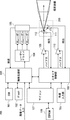
- FIG. 1 is a block diagram illustrating a configuration of an image display device according to a first embodiment
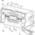
- FIG. 3 is a perspective view illustrating a configuration of a scanning mirror of the image display apparatus according to the first embodiment.
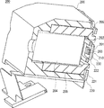
- FIG. 3 is a cross-sectional view illustrating a configuration of a scanning mirror of the image display apparatus according to the first embodiment.
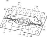
- FIG. 3 is a perspective view illustrating a configuration of a back surface of an FPC board of a scanning mirror in the image display apparatus according to the first embodiment.
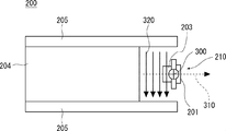
- it is a diagram illustrating a state in which a reflection surface of a scanning mirror is parallel to a magnetic field.
- FIG. 3 is a diagram illustrating the direction of a reflecting surface at a design value of the image display apparatus according to the first embodiment.
- it is a diagram illustrating a state in which the orientation of the reflecting surface is deviated from the design value.
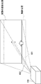
- FIG. 3 is a diagram for explaining a shift of a projected image in the image display apparatus according to the first embodiment.
- 3 is a flowchart illustrating an image display method according to the first exemplary embodiment.
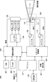
- FIG. 3 is a block diagram illustrating a configuration of an image display apparatus according to a second embodiment.
- FIG. 6 is a block diagram illustrating a configuration of an image display device according to a third embodiment.
- FIG. 1 is a block diagram illustrating a configuration of an image display apparatus 100 according to the present embodiment.
- the image display apparatus 100 includes a DDR (Double Data Rate) memory 101, a flash memory 102, an image processing unit 103, a laser driver 104, an RGB laser diode 105, an EEPROM (Electrically Erasable and Programmable Read Only Memory) 106, A microcomputer 107, a scanner control unit 108, a vertical scanner driver 109, a horizontal scanner driver 110, and a scanning mirror 200.
- the vertical direction of the image to be displayed is also referred to as the V (Vertical) axis direction
- the horizontal direction of the image is also referred to as the H (Horizontal) axis direction.
- the DDR memory 101 is a frame buffer that temporarily stores image data input to the image processing unit 103.
- the DDR memory 101 may be DDR2, DDR3, or other SDRAM.
- the flash memory 102 is a nonvolatile storage unit that stores data and programs necessary for the operation of the image processing unit 103.
- the image processing unit 103 performs processing such as data rearrangement on the image data input from the DDR memory 101 and outputs the processed data to the laser driver 104 and the scanner control unit 108.
- the image processing unit 103 may be realized by hardware such as FPGA (Field Programmable Gate Gate Array) or may be realized by a program stored in the flash memory 102 and a CPU (Central Processing Unit).
- the laser driver 104 drives the RGB laser diode 105 according to the input image data supplied from the image processing unit 103.
- the laser driver 104 is a light source driving unit that drives the RGB laser diode 105 based on input image data at a timing determined by the image processing unit 103.
- the light source driving unit drives the light source unit based on the input image data.
- the RGB laser diode 105 emits laser light of three colors of red (R), green (G), and blue (B) by driving the laser driver 104.
- the RGB laser diode 105 is a light source unit that outputs laser light that is a light beam.
- the RGB laser diode 105 creates various colors used in the projected image by controlling the emission intensity and emission time of each color.
- the microcomputer 107 generates a drive signal for operating the scanner control unit 108 and outputs the generated drive signal to the scanner control unit 108.
- the EEPROM 106 is a nonvolatile storage unit that stores data and programs necessary for the operation of the scanner control unit 108.
- the scanner control unit 108 controls the deflection angle of the scanning mirror 200, the scanning frequency, and the like.
- the scanner control unit 108 generates a drive voltage waveform so that the scanning mirror 200 can obtain a desired deflection angle, frequency, and the like.
- the scanner control unit 108 may be realized by hardware such as an FPGA, or may be realized by a program stored in the flash memory 102 and a CPU.
- the scanning mirror 200 scans the light beam by reflecting the light beam at an angle corresponding to the driving voltage.
- the scanning mirror 200 includes a horizontal scanner 111 and a vertical scanner 112.
- the vertical scanner 112 scans the light beam in the vertical direction
- the horizontal scanner 111 scans the light beam in the horizontal direction.
- the vertical scanner driver 109 swings the vertical scanner 112 according to the vertical drive signal supplied from the image processing unit 103.
- the horizontal scanner driver 110 swings the horizontal scanner 111 in accordance with a horizontal drive signal supplied from the scanner control unit 108.
- the vertical scanner 112 is an optical scanner that reflects the laser light emitted from the RGB laser diode 105 and swings based on a signal from the vertical scanner driver 109 to scan the light beam in the vertical direction.
- the horizontal scanner 111 is an optical scanner that reflects the laser light emitted from the RGB laser diode 105 and scans the light flux in the horizontal direction by swinging based on a signal from the horizontal scanner driver 110.
- the horizontal scanner 111 reflects the laser light from the RGB laser diode 105, and the vertical scanner 112 further reflects the reflected light from the horizontal scanner 111, thereby drawing a projected image on the projection surface.
- the vertical scanner 112 and the horizontal scanner 111 constitute an optical scanner that reciprocates in the vertical and horizontal directions.
- the vertical scanner 112 and the horizontal scanner 111 may be a single two-axis (two-dimensional) optical scanner.
- the vertical scanner 112 and the horizontal scanner 111 can use various methods such as a piezoelectric film method and a coil driving method.
- FIG. 2 is a perspective view illustrating the configuration of the scanning mirror 200 of the image display apparatus 100.
- FIG. 2 shows the scanning mirror 200 viewed from the front side.
- FIG. 3 is a cross-sectional view illustrating the configuration of the scanning mirror 200 of the image display apparatus 100.
- FIG. 4 is a perspective view showing the configuration of the back surface of the scanning mirror 200.
- the scanning mirror 200 includes a case 206, an FPC (Flexible printed circuits) substrate 220, a magnet 204, and a yoke 205. As shown in FIG. 3, a magnet 204 and a yoke 205 are accommodated in the case 206.
- the magnet 204 generates a magnetic field.
- the yoke 205 is provided around the magnet 204.
- the yoke 205 concentrates the magnetic field generated by the magnet 204 around the reflecting mirror 230.
- An FPC board 220 is attached to the front surface of the case 206.
- the FPC board 220 includes a frame portion 221, a base 222, a beam 223, a terminal 224, and a wiring 225.
- the frame part 221, the base 222, and the beam 223 are integrally formed.
- a base 222 is supported inside the frame portion 221 via a beam 223.
- the base 222 and the frame portion 221 may be reinforced by a backing material such as a polyimide plate.
- the beam 223 is provided between the base 222 and the frame portion 221, and supports the base 222 in a swingable manner about the mirror rotation shaft 300.
- a reflecting mirror 230 is provided on the front surface of the base 222, and a driving coil 202 and a hall element 203 are provided on the back surface.
- the reflecting mirror 230 has a reflecting surface 201 that reflects light.
- the driving coil 202 is provided so as to surround the hall element 203.
- the mirror unit 210 is configured by the reflecting mirror 230, the base 222, the driving coil 202, and the Hall element 203. In the mirror part 210, since the driving coil 202 is provided on the back side of the base 222 and the back side becomes heavy, the base 222 is easily inclined to the back side by gravity.
- the terminal 224 and the wiring 225 are formed of a conductive member such as copper, and include a circuit that guides an electrical signal from an external circuit to the driving coil 202 and a circuit that guides a detection signal from the Hall element 203 to the external circuit. Constitute.
- An external circuit is connected to the terminal 224, and an electric signal input from the terminal 224 is input to the driving coil 202 through the wiring 225.
- the detection signal output from the hall element 203 is output to an external circuit via the wiring 225 and the terminal 224.
- the driving coil 202 When a voltage is applied to the driving coil 202 from the scanner control unit 108, the driving coil 202 receives a Lorentz force from the magnetic field generated by the magnet 204, so the direction of the base 222 is changed according to the driving voltage, and the base 222 swings around the mirror rotation axis 300.
- the hall element 203 is provided on the back surface of the base 222 and detects the magnetic field strength of the magnet 204.
- the image display device 100 detects a static angle based on the magnetic field strength detected by the Hall element 203.
- the hall element 203 functions as a static angle detection unit.
- the static angle refers to an angle at which the scanning mirror 200 stops when no driving voltage is applied.
- the Hall element 203 detects the rotation angle of the scanning mirror 200
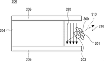
- the magnetic field 320 generated by the magnet 204 is concentrated on the mirror unit 210 of the scanning mirror 200 using the yoke 205.
- the mirror unit 210 swings about the mirror rotation axis 300.
- the mirror unit 210 includes a reflective surface 201 and a Hall element 203 provided on the surface opposite to the reflective surface 201.
- the Hall element 203 can detect the magnetic field in the normal direction of the detection surface.
- the magnetic field detection axis 310 of the Hall element 203 faces rightward in the drawing, and the magnetic field detection axis 310 and the magnetic field 320 are orthogonal to each other, so that the magnetic field detected by the Hall element 203 is zero.
- the scanner control unit 108 adds a bias voltage based on the static angle detected by the Hall element 203 to the drive voltage.
- the scanner control unit 108 functions as a bias application unit that applies a bias voltage.
- the scanner control unit 108 may apply a bias voltage to the scanning mirror 200 based on a static angle at which the scanning mirror 200 stops when no driving voltage is applied or an angle with respect to a horizontal plane.
- the angle with respect to the horizontal plane here is an angle between the central axis of the reflection surface of the scanning mirror 200 and the horizontal plane, which is generally determined by the installation angle at which the image display device 100 is installed. As shown in FIG.
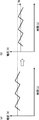
- FIG. 8 is a diagram illustrating a change in the driving voltage before and after applying the bias voltage.
- FIG. 8A shows the drive voltage before applying the bias voltage
- FIG. 8B shows the drive voltage after applying the bias voltage.
- the drive voltage is reduced by the bias voltage Vb as compared to FIG. 8A.
- the bias voltage may be positive or negative.
- the waveform of the drive voltage for example, a sine wave, a ramp waveform, or the like can be used.
- the normal line of the reflecting surface 201 of the scanning mirror 200 that is stopped is the horizontal plane. Should be parallel.
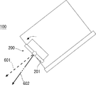
- the mechanical center axis 601 is an axis indicating the design position of the center in the vertical direction of the projection image projected by the image display apparatus 100.
- the driving coil 202 is provided on the back side opposite to the reflecting surface 201 in the scanning mirror 200, the back side becomes heavy. Therefore, as shown in FIG. 10, even if the image display apparatus 100 is installed so that the mechanical center axis 601 is parallel to the horizontal plane, the reflection surface 201 of the scanning mirror 200 is inclined by gravity.
- the normal line located at the center of the reflection surface 201 at this time is defined as a reflection surface central axis 602.
- the image display device 100 cannot always be installed so that the reflection surface central axis 602 of the scanning mirror 200 is parallel to the horizontal plane, and there are cases where the image display device 100 has to be installed on an inclined installation surface.
- FIG. 11 when the laser beam emission side of the image display device 100 is installed so as to be directed upward, the reflection surface central axis 602 of the scanning mirror 200 is inclined upward.
- FIG. 12 when the laser beam emitting side of the image display device 100 is installed so as to face downward, the reflection surface central axis 602 of the scanning mirror 200 tilts further downward.
- the inclination of the reflection surface 201 of the scanning mirror 200 changes depending on the installation conditions of the image display apparatus 100.
- the projected image is also shifted upward from the design position as shown in FIG.
- the deviation of the projected image differs for each individual image display apparatus 100, and the amount of deviation due to a change with time varies for each individual.
- FIG. 14 is a flowchart illustrating an image display method using the image display apparatus 100.
- the Hall element 203 detects a static angle at which the scanning mirror 200 stops when no driving voltage is applied (ST401).
- scanner control section 108 adds the calculated bias voltage to the drive voltage (ST404).
- scanner control section 108 scans the light beam by applying a drive voltage to which a bias voltage has been applied to scanning mirror 200 (ST405).
- the tilt of the reflecting surface 201 in the stationary state of the scanning mirror 200 is detected by the Hall element 203, and a bias voltage necessary for correcting the tilt is calculated.
- a drive voltage plus a bias voltage can be applied to the scanning mirror.
- the image display apparatus 100 can adjust so that the center of a projection image may come to a design position, when projecting an image.
- the image display device 700 is different from the image display device 100 according to the first embodiment in that the image display device 700 includes an angle input unit 701.
- the angle input unit 701 receives an angle formed by the reflection plane central axis 601 of the scanning mirror 200 and the horizontal plane, which is generated depending on the installation angle of the image display device 700.
- the angle of the image display device 700 formed by the reflection surface central axis 601 and the horizontal plane is measured using an angle measuring instrument and input to the angle input unit 701 before the image display device 700 is used.
- the angle between the reflecting surface center axis 601 and the horizontal plane associated with the input angle may be input to the angle input unit 701 by inputting the installation angle of the image display device 700.
- the flash memory 102 stores an angle-bias voltage table that represents the relationship between the angle with respect to the horizontal plane and the intensity of the bias voltage.
- the angle-bias voltage table when a certain angle is formed between the reflection surface central axis 601 of the scanning mirror 200 and the horizontal plane, the magnitude of the bias voltage can be applied to correct the projection image to the design position. Is a table.
- the scanner control unit 108 adds a bias voltage to the drive voltage based on the angle input to the angle input unit 701 and the angle-bias voltage table.
- the image display device 700 can correct the position of the projection image without knowing the static angle of the reflection surface 201 of the scanning mirror 200. Therefore, it is not necessary to provide an angle sensor such as the Hall element 203 in the scanning mirror 200, so that the cost of the scanning mirror 200 can be reduced.
- the image display apparatus 800 is different from the image display apparatus 100 according to the first embodiment in that the image display apparatus 800 includes an angle detection unit 801.
- the angle detection unit 801 detects an angle formed by the reflection surface central axis 601 of the scanning mirror 200 and the horizontal plane, which is generated by the installation angle of the image display device 800.
- an angle sensor such as a gyro is used as the angle detection unit 801 .
- the angle detection unit 801 detects an installation angle of the image display device 800, for example, and detects an angle formed by the reflection surface central axis 601 of the scanning mirror 200 and the horizontal plane based on the detected installation angle.
- the flash memory 102 stores an angle-bias voltage table that represents the relationship between the angle and the intensity of the bias voltage.
- the scanner control unit 108 adds a bias voltage to the drive voltage based on the angle detected by the angle detection unit 801 and the angle-bias voltage table.
- the position of the projection image can be corrected without knowing the static angle of the reflection surface 201 of the scanning mirror 200. Therefore, it is not necessary to provide an angle sensor such as the Hall element 203 in the scanning mirror 200, so that the cost of the scanning mirror 200 can be reduced. Further, as compared with the image display device 700 according to the second embodiment, it is not necessary to measure the angle of the image display device 800 with respect to the horizontal plane in advance, and the image display device 800 detects the angle with respect to the horizontal plane by itself. The center position can be easily corrected.
- the present invention is not limited to the above-described embodiment, and can be appropriately changed without departing from the spirit of the present invention.
- the deviation from the center angle of the scanning mirror 200 has been described by taking the vertical scanner 112 as an example.
Landscapes
- Physics & Mathematics (AREA)
- Optics & Photonics (AREA)
- Engineering & Computer Science (AREA)
- Multimedia (AREA)
- Signal Processing (AREA)
- General Physics & Mathematics (AREA)
- Geometry (AREA)
- Mechanical Optical Scanning Systems (AREA)
- Mechanical Light Control Or Optical Switches (AREA)
- Transforming Electric Information Into Light Information (AREA)
Abstract
Description
また、特許文献2に記載の画像表示装置では、走査ミラーの反射面の裏面にホール素子を備えて、ホール素子により測定される磁界強度に基づいて反射面の角度を検出している。
光束を出力する光源部と、
入力画像データに基づき前記光源部を駆動させる光源駆動部と、
駆動電圧に応じた角度で前記光束を反射することにより、前記光束を走査する走査ミラーと、を備える画像表示装置であって、
前記駆動電圧を印加されないときに前記走査ミラーが停止する静的角度、又は、水平面に対する前記画像表示装置の角度に基づいて、バイアス電圧を前記走査ミラーに印加するバイアス印加部と、
を備える。
光束を出力する光源部と、入力画像データに基づき前記光源部を駆動させる光源駆動部と、駆動電圧に応じた角度で前記光束を反射することにより前記光束を走査する走査ミラーと、を備える画像表示装置における画像表示方法であって、
前記駆動電圧を印加されないときに前記走査ミラーが停止する静的角度、又は、水平面に対する角度を取得し、
前記静的角度又は水平面に対する角度に基づいて、前記駆動電圧に加えるバイアス電圧を算出し、
前記バイアス電圧が加えられた前記駆動電圧を前記走査ミラーに印加することにより、前記光束を走査させる
ことを特徴とする。
以下、図面を参照して本発明の実施の形態について説明する。
図1は、本実施の形態の画像表示装置100の構成を示すブロック図である。
画像表示装置100は、DDR(Double Data Rate)メモリ101と、フラッシュメモリ102と、画像処理部103と、レーザードライバ104と、RGBレーザーダイオード105と、EEPROM(Electrically Erasable and Programmable Read Only Memory)106と、マイコン107と、スキャナ制御部108と、垂直スキャナドライバ109と、水平スキャナドライバ110と、走査ミラー200と、を備える。なお、表示する画像の垂直方向をV(Vertical)軸方向とも称し、画像の水平方向をH(Horizontal)軸方向とも称する。
フラッシュメモリ102は、画像処理部103の動作に必要なデータやプログラムなどを記憶する不揮発性記憶部である。
EEPROM106は、スキャナ制御部108の動作に必要なデータやプログラムなどを記憶する不揮発性記憶部である。
図2は、画像表示装置100の走査ミラー200の構成を表す斜視図である。図2は、走査ミラー200を前面側から見た状態を示す。図3は、画像表示装置100の走査ミラー200の構成を表す断面図である。図4は、走査ミラー200の裏面の構成を示す斜視図である。
図3に示すように、ケース206内に、マグネット204と、ヨーク205と、が収納されている。マグネット204は磁界を発生させる。ヨーク205はマグネット204の周囲に設けられている。ヨーク205は、マグネット204が発生する磁界を反射鏡230の周囲へと集中させる。ケース206の前面には、FPC基板220が取り付けられている。
図5に示すように、ヨーク205を用いて、マグネット204が発生する磁界320を走査ミラー200のミラー部210へと集中させる。ミラー部210は、ミラー回転軸300を中心として揺動する。ミラー部210は、反射面201と、反射面201の反対側の面に設けられたホール素子203と、を有する。ホール素子203は、その検出面の法線方向の磁界を検出することができる。図5においては、ホール素子203の磁界検出軸310は、紙面右方向を向いており、磁界検出軸310と磁界320が直交しているので、ホール素子203により検出される磁界はゼロである。
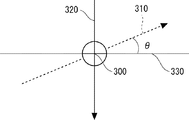
図7に示すように磁界320に直交する軸330と磁界検出軸310がなす角度がθ(°)のときに、ホール素子の出力電圧Vh(V)は、磁束密度をB(T)、ホール電流をIh(A)、係数をK(V・A-1・T-1)とすると、Vh=K・Ih・B・sinθで算出される。
なお、バイアス電圧はプラスマイナスの極性は問わない。駆動電圧の波形は、例えば、正弦波、ランプ波形等を用いることができる。
図14は、画像表示装置100を用いた画像表示方法を示すフローチャートである。
ホール素子203が、駆動電圧を印加されないときに走査ミラー200が停止する静的角度を検出する(ST401)。
次に、スキャナ制御部108は、バイアス電圧が加えられた駆動電圧を走査ミラー200に印加することにより、光束を走査させる(ST405)。
なお、バイアス電圧を加えた後に、バイアス電圧により走査ミラー200の反射面201が中心角度と一致するかを、走査ミラー200からの検出信号により確認する工程を追加してもよい。
図15を用いて、本実施の形態にかかる画像表示装置700について説明する。
画像表示装置700は、角度入力部701を有する点が、実施の形態1にかかる画像表示装置100とは異なる。
角度入力部701は、画像表示装置700の設置角度によって生じる、走査ミラー200の反射面中心軸601と水平面とがなす角度が入力される。反射面中心軸601と水平面とがなす画像表示装置700の角度は、角度計測器を用いて測定され、画像表示装置700の使用前に角度入力部701に入力される。または、画像表示装置700の設置角度を入力することにより、入力角度に対応付けられた反射面中心軸601と水平面との角度が角度入力部701に入力されるようにしてもよい。
スキャナ制御部108は、角度入力部701に入力された角度と、角度-バイアス電圧テーブルに基づいて、駆動電圧にバイアス電圧を加える。
図16を用いて、本実施の形態にかかる画像表示装置800について説明する。
画像表示装置800は、角度検出部801を有する点が、実施の形態1にかかる画像表示装置100とは異なる。
角度検出部801は、画像表示装置800の設置角度によって生じる、走査ミラー200の反射面中心軸601と水平面とがなす角度を検出する。角度検出部801としては、ジャイロ等の角度センサが用いられる。角度検出部801は、例えば画像表示装置800の設置角度を検出し、検出した設置角度に基づいて走査ミラー200の反射面中心軸601と水平面とがなす角度を検出する。
スキャナ制御部108は、角度検出部801により検出された角度と、角度-バイアス電圧テーブルに基づいて、駆動電圧にバイアス電圧を加える。
また、実施の形態2にかかる画像表示装置700と比較すると、画像表示装置800の水平面に対する角度を事前に測定する必要がなく、画像表示装置800が自ら水平面に対する角度を検出するので、投影画像の中心位置の補正が簡単にできる。
101 メモリ
102 フラッシュメモリ
103 画像処理部
104 レーザードライバ
105 レーザーダイオード
107 マイコン
108 スキャナ制御部
109 垂直スキャナドライバ
110 水平スキャナドライバ
111 水平スキャナ
112 垂直スキャナ
200 走査ミラー
201 反射面
202 駆動用コイル
203 ホール素子
204 マグネット
205 ヨーク
210 ミラー部
230 反射鏡
701 角度入力部
801 角度検出部
Claims (6)
- 光束を出力する光源部と、
入力画像データに基づき前記光源部を駆動させる光源駆動部と、
駆動電圧に応じた角度で前記光束を反射することにより、前記光束を走査する走査ミラーと、を備える画像表示装置であって、
前記駆動電圧を印加されないときに前記走査ミラーが停止する静的角度、又は、水平面に対する角度に基づいて、バイアス電圧を前記走査ミラーに印加するバイアス印加部と、
を備える画像表示装置。 - 請求項1に記載の画像表示装置であって、
前記静的角度を検出する静的角度検出部をさらに備え、
前記バイアス印加部は、前記静的角度検出部により検出された前記静的角度に基づくバイアス電圧を前記駆動電圧に加える
ことを特徴とする画像表示装置。 - 請求項2に記載の画像表示装置であって、
前記画像表示装置は、
前記走査ミラーの反射面の裏面に設けられており、前記駆動電圧に応じて前記反射面の向きを変更する駆動用コイルと、
前記駆動用コイルの周囲に磁界を発生させるマグネットと、を備え、
前記静的角度検出部は、
前記走査ミラーの反射面の裏面に設けられ、前記マグネットの磁界強度を検出するホール素子を有し、
前記ホール素子により検出される磁界強度に基づいて、前記静的角度を検出する
ことを特徴とする画像表示装置。 - 請求項1に記載の画像表示装置であって、
水平面に対する角度を入力する角度入力部と、
水平面に対する角度とバイアス電圧の強度との関係を表す角度-バイアス電圧テーブルを記憶する記憶部と、を備え、
前記バイアス印加部が、前記角度入力部に入力された角度と、前記角度-バイアス電圧テーブルに基づいて、前記駆動電圧にバイアス電圧を加える
ことを特徴とする画像表示装置。 - 請求項1に記載の画像表示装置であって、
前記画像表示装置の水平面に対する角度を検出する角度検出部と、
水平面に対する角度とバイアス電圧の強度との関係を表す角度-バイアス電圧テーブルを記憶する記憶部と、を備え、
前記バイアス印加部が、前記角度検出部により検出された角度と、前記角度-バイアス電圧テーブルに基づいて、前記駆動電圧にバイアス電圧を加える
ことを特徴とする画像表示装置。 - 光束を出力する光源部と、入力画像データに基づき前記光源部を駆動させる光源駆動部と、駆動電圧に応じた角度で前記光束を反射することにより前記光束を走査する走査ミラーと、を備える画像表示装置における画像表示方法であって、
前記駆動電圧を印加されないときに前記走査ミラーが停止する静的角度、又は、水平面に対する角度を取得し、
前記静的角度又は水平面に対する角度に基づいて、前記駆動電圧に加えるバイアス電圧を算出し、
前記バイアス電圧が加えられた前記駆動電圧を前記走査ミラーに印加することにより、前記光束を走査させる
ことを特徴とする画像表示方法。
Priority Applications (3)
| Application Number | Priority Date | Filing Date | Title |
|---|---|---|---|
| JP2016503790A JPWO2015125190A1 (ja) | 2014-02-20 | 2014-10-28 | 画像表示装置および画像表示方法 |
| EP14883402.1A EP3109686B1 (en) | 2014-02-20 | 2014-10-28 | Image display device and image display method |
| US15/240,948 US10104350B2 (en) | 2014-02-20 | 2016-08-18 | Image display device and image display method |
Applications Claiming Priority (2)
| Application Number | Priority Date | Filing Date | Title |
|---|---|---|---|
| JP2014-030126 | 2014-02-20 | ||
| JP2014030126 | 2014-02-20 |
Related Child Applications (1)
| Application Number | Title | Priority Date | Filing Date |
|---|---|---|---|
| US15/240,948 Continuation US10104350B2 (en) | 2014-02-20 | 2016-08-18 | Image display device and image display method |
Publications (1)
| Publication Number | Publication Date |
|---|---|
| WO2015125190A1 true WO2015125190A1 (ja) | 2015-08-27 |
Family
ID=53877731
Family Applications (1)
| Application Number | Title | Priority Date | Filing Date |
|---|---|---|---|
| PCT/JP2014/005432 Ceased WO2015125190A1 (ja) | 2014-02-20 | 2014-10-28 | 画像表示装置および画像表示方法 |
Country Status (4)
| Country | Link |
|---|---|
| US (1) | US10104350B2 (ja) |
| EP (1) | EP3109686B1 (ja) |
| JP (1) | JPWO2015125190A1 (ja) |
| WO (1) | WO2015125190A1 (ja) |
Cited By (2)
| Publication number | Priority date | Publication date | Assignee | Title |
|---|---|---|---|---|
| JP2017067907A (ja) * | 2015-09-29 | 2017-04-06 | 株式会社Jvcケンウッド | 光スキャナ |
| JP2019219460A (ja) * | 2018-06-18 | 2019-12-26 | 株式会社リコー | 画像投射装置、及び画像投射方法 |
Families Citing this family (2)
| Publication number | Priority date | Publication date | Assignee | Title |
|---|---|---|---|---|
| US20170148394A1 (en) * | 2015-11-23 | 2017-05-25 | Le Holdings (Beijing) Co., Ltd. | System and method for controlling dynamic backlight source of eled |
| CN108635025B (zh) * | 2018-07-24 | 2023-09-05 | 无锡市第二人民医院 | 一种激光穿刺引导系统 |
Citations (4)
| Publication number | Priority date | Publication date | Assignee | Title |
|---|---|---|---|---|
| JP2002307396A (ja) * | 2001-04-13 | 2002-10-23 | Olympus Optical Co Ltd | アクチュエータ |
| JP2008046453A (ja) * | 2006-08-18 | 2008-02-28 | Nippon Telegr & Teleph Corp <Ntt> | ミラー制御装置およびミラー制御方法 |
| JP2011170658A (ja) * | 2010-02-19 | 2011-09-01 | Seiko Epson Corp | 画像形成装置 |
| JP2012198314A (ja) * | 2011-03-18 | 2012-10-18 | Ricoh Co Ltd | アクチュエータ装置、光偏向装置、光走査装置、画像形成装置及び画像投影装置 |
Family Cites Families (16)
| Publication number | Priority date | Publication date | Assignee | Title |
|---|---|---|---|---|
| JP2779053B2 (ja) * | 1990-09-25 | 1998-07-23 | 株式会社日立製作所 | 光走査装置 |
| US5646765A (en) * | 1994-10-05 | 1997-07-08 | Synrad, Inc. | Laser scanner |
| JP2000081589A (ja) | 1998-07-09 | 2000-03-21 | Olympus Optical Co Ltd | 光偏向器 |
| US6771851B1 (en) * | 2001-06-19 | 2004-08-03 | Nayna Networks | Fast switching method for a micro-mirror device for optical switching applications |
| US7034370B2 (en) * | 2002-11-22 | 2006-04-25 | Advanced Nano Systems, Inc. | MEMS scanning mirror with tunable natural frequency |
| US6769616B2 (en) * | 2002-11-22 | 2004-08-03 | Advanced Nano Systems | Bidirectional MEMS scanning mirror with tunable natural frequency |
| JP2005181580A (ja) * | 2003-12-18 | 2005-07-07 | Olympus Corp | 光スイッチ装置とそのキャリブレーション方法 |
| JP2006087208A (ja) * | 2004-09-15 | 2006-03-30 | Canon Inc | モータ装置および光学走査装置 |
| JP5151065B2 (ja) | 2006-05-19 | 2013-02-27 | コニカミノルタホールディングス株式会社 | 光スキャナ及び走査型プロジェクタ |
| KR20090051859A (ko) * | 2007-11-20 | 2009-05-25 | 삼성전기주식회사 | 스캐너 및 이를 구비하는 디스플레이 장치 |
| WO2010021215A1 (ja) * | 2008-08-18 | 2010-02-25 | コニカミノルタオプト株式会社 | 画像投影装置 |
| US8451308B2 (en) * | 2009-07-31 | 2013-05-28 | Ricoh Company, Ltd. | Image forming apparatus |
| JP2011215324A (ja) * | 2010-03-31 | 2011-10-27 | Brother Industries Ltd | 光走査装置及び画像表示装置 |
| US9778458B2 (en) * | 2010-09-30 | 2017-10-03 | Xerox Corporation | Software control of LED illumination output for improved yield and latitude |
| US9607363B2 (en) * | 2012-06-19 | 2017-03-28 | Ricoh Company, Ltd. | Projector, trapezoidal distortion correction method, and storage medium storing trapezoidal distortion correction program |
| JP6053171B2 (ja) * | 2013-10-18 | 2016-12-27 | 増田 麻言 | 走査型投影装置、および携帯型投影装置 |
-
2014
- 2014-10-28 JP JP2016503790A patent/JPWO2015125190A1/ja active Pending
- 2014-10-28 WO PCT/JP2014/005432 patent/WO2015125190A1/ja not_active Ceased
- 2014-10-28 EP EP14883402.1A patent/EP3109686B1/en active Active
-
2016
- 2016-08-18 US US15/240,948 patent/US10104350B2/en active Active
Patent Citations (4)
| Publication number | Priority date | Publication date | Assignee | Title |
|---|---|---|---|---|
| JP2002307396A (ja) * | 2001-04-13 | 2002-10-23 | Olympus Optical Co Ltd | アクチュエータ |
| JP2008046453A (ja) * | 2006-08-18 | 2008-02-28 | Nippon Telegr & Teleph Corp <Ntt> | ミラー制御装置およびミラー制御方法 |
| JP2011170658A (ja) * | 2010-02-19 | 2011-09-01 | Seiko Epson Corp | 画像形成装置 |
| JP2012198314A (ja) * | 2011-03-18 | 2012-10-18 | Ricoh Co Ltd | アクチュエータ装置、光偏向装置、光走査装置、画像形成装置及び画像投影装置 |
Non-Patent Citations (1)
| Title |
|---|
| See also references of EP3109686A4 * |
Cited By (3)
| Publication number | Priority date | Publication date | Assignee | Title |
|---|---|---|---|---|
| JP2017067907A (ja) * | 2015-09-29 | 2017-04-06 | 株式会社Jvcケンウッド | 光スキャナ |
| JP2019219460A (ja) * | 2018-06-18 | 2019-12-26 | 株式会社リコー | 画像投射装置、及び画像投射方法 |
| JP7040310B2 (ja) | 2018-06-18 | 2022-03-23 | 株式会社リコー | 画像投射装置、及び画像投射方法 |
Also Published As
| Publication number | Publication date |
|---|---|
| EP3109686A4 (en) | 2017-01-25 |
| JPWO2015125190A1 (ja) | 2017-03-30 |
| US10104350B2 (en) | 2018-10-16 |
| EP3109686A1 (en) | 2016-12-28 |
| US20160360170A1 (en) | 2016-12-08 |
| EP3109686B1 (en) | 2022-12-28 |
Similar Documents
| Publication | Publication Date | Title |
|---|---|---|
| US7835053B2 (en) | Projection image display apparatus | |
| EP2848449A1 (en) | Image generation apparatus, vehicle, control method of image generation apparatus and carrier medium | |
| JP5115044B2 (ja) | 画像表示装置及び画像表示方法 | |
| CN112578614A (zh) | 光学器件、投影仪以及光学器件的控制方法 | |
| JP5417915B2 (ja) | レーザプロジェクタ | |
| JP6287808B2 (ja) | 画像表示装置及び画像補正方法 | |
| US20120313909A1 (en) | Display apparatus | |
| JP2010261979A (ja) | レーザプロジェクタ | |
| WO2015125190A1 (ja) | 画像表示装置および画像表示方法 | |
| CN107924115A (zh) | 扫描显示系统中的投影内容的亮度或大小的动态稳定性 | |
| US8379282B2 (en) | Light scanning unit and method of detecting scanning synchronization signal | |
| CN111190280A (zh) | 光路移位设备、图像显示装置及光路移位设备的控制方法 | |
| JP5234514B2 (ja) | 画像形成装置 | |
| US9575397B2 (en) | Optical member driving device and projection image display apparatus | |
| JP2009237239A (ja) | 光スキャナ装置および画像形成装置 | |
| JP5312302B2 (ja) | 光走査装置 | |
| JP2018177015A (ja) | 車両用表示装置 | |
| JP4203037B2 (ja) | ダイナミックアパーチャー駆動装置及びその制御方法 | |
| JP6961502B2 (ja) | 光走査装置 | |
| JP2009222857A (ja) | 光スキャナ装置および画像形成装置 | |
| JP2021033011A (ja) | 光走査装置、光走査方法およびプログラム | |
| JP2009237102A (ja) | 光スキャナ装置および画像形成装置 | |
| JP4316271B2 (ja) | 光走査装置 | |
| JP2008233449A (ja) | 光ビーム走査装置および画像形成装置 | |
| JP2012145754A (ja) | 画像表示装置 |
Legal Events
| Date | Code | Title | Description |
|---|---|---|---|
| 121 | Ep: the epo has been informed by wipo that ep was designated in this application |
Ref document number: 14883402 Country of ref document: EP Kind code of ref document: A1 |
|
| ENP | Entry into the national phase |
Ref document number: 2016503790 Country of ref document: JP Kind code of ref document: A |
|
| NENP | Non-entry into the national phase |
Ref country code: DE |
|
| REEP | Request for entry into the european phase |
Ref document number: 2014883402 Country of ref document: EP |
|
| WWE | Wipo information: entry into national phase |
Ref document number: 2014883402 Country of ref document: EP |