WO2015125226A1 - 対基板作業システム及び対基板作業システムの部品の装着順を管理する方法 - Google Patents
対基板作業システム及び対基板作業システムの部品の装着順を管理する方法 Download PDFInfo
- Publication number
- WO2015125226A1 WO2015125226A1 PCT/JP2014/053884 JP2014053884W WO2015125226A1 WO 2015125226 A1 WO2015125226 A1 WO 2015125226A1 JP 2014053884 W JP2014053884 W JP 2014053884W WO 2015125226 A1 WO2015125226 A1 WO 2015125226A1
- Authority
- WO
- WIPO (PCT)
- Prior art keywords
- die
- wafer
- mounting
- supply
- control device
- Prior art date
- Legal status (The legal status is an assumption and is not a legal conclusion. Google has not performed a legal analysis and makes no representation as to the accuracy of the status listed.)
- Ceased
Links
Images






Classifications
-
- H—ELECTRICITY
- H05—ELECTRIC TECHNIQUES NOT OTHERWISE PROVIDED FOR
- H05K—PRINTED CIRCUITS; CASINGS OR CONSTRUCTIONAL DETAILS OF ELECTRIC APPARATUS; MANUFACTURE OF ASSEMBLAGES OF ELECTRICAL COMPONENTS
- H05K13/00—Apparatus or processes specially adapted for manufacturing or adjusting assemblages of electric components
- H05K13/08—Monitoring manufacture of assemblages
-
- H—ELECTRICITY
- H05—ELECTRIC TECHNIQUES NOT OTHERWISE PROVIDED FOR
- H05K—PRINTED CIRCUITS; CASINGS OR CONSTRUCTIONAL DETAILS OF ELECTRIC APPARATUS; MANUFACTURE OF ASSEMBLAGES OF ELECTRICAL COMPONENTS
- H05K13/00—Apparatus or processes specially adapted for manufacturing or adjusting assemblages of electric components
- H05K13/04—Mounting of components, e.g. of leadless components
- H05K13/043—Feeding one by one by other means than belts
- H05K13/0434—Feeding one by one by other means than belts with containers
-
- H—ELECTRICITY
- H05—ELECTRIC TECHNIQUES NOT OTHERWISE PROVIDED FOR
- H05K—PRINTED CIRCUITS; CASINGS OR CONSTRUCTIONAL DETAILS OF ELECTRIC APPARATUS; MANUFACTURE OF ASSEMBLAGES OF ELECTRICAL COMPONENTS
- H05K13/00—Apparatus or processes specially adapted for manufacturing or adjusting assemblages of electric components
- H05K13/08—Monitoring manufacture of assemblages
- H05K13/085—Production planning, e.g. of allocation of products to machines, of mounting sequences at machine or facility level
-
- H—ELECTRICITY
- H10—SEMICONDUCTOR DEVICES; ELECTRIC SOLID-STATE DEVICES NOT OTHERWISE PROVIDED FOR
- H10P—GENERIC PROCESSES OR APPARATUS FOR THE MANUFACTURE OR TREATMENT OF DEVICES COVERED BY CLASS H10
- H10P72/00—Handling or holding of wafers, substrates or devices during manufacture or treatment thereof
- H10P72/04—Apparatus for manufacture or treatment
- H10P72/0442—Apparatus for placing on an insulating substrate, e.g. tape
-
- H—ELECTRICITY
- H10—SEMICONDUCTOR DEVICES; ELECTRIC SOLID-STATE DEVICES NOT OTHERWISE PROVIDED FOR
- H10W—GENERIC PACKAGES, INTERCONNECTIONS, CONNECTORS OR OTHER CONSTRUCTIONAL DETAILS OF DEVICES COVERED BY CLASS H10
- H10W72/00—Interconnections or connectors in packages
- H10W72/071—Connecting or disconnecting
- H10W72/0711—Apparatus therefor
- H10W72/07173—Means for moving chips, wafers or other parts, e.g. conveyor belts
-
- Y—GENERAL TAGGING OF NEW TECHNOLOGICAL DEVELOPMENTS; GENERAL TAGGING OF CROSS-SECTIONAL TECHNOLOGIES SPANNING OVER SEVERAL SECTIONS OF THE IPC; TECHNICAL SUBJECTS COVERED BY FORMER USPC CROSS-REFERENCE ART COLLECTIONS [XRACs] AND DIGESTS
- Y10—TECHNICAL SUBJECTS COVERED BY FORMER USPC
- Y10T—TECHNICAL SUBJECTS COVERED BY FORMER US CLASSIFICATION
- Y10T29/00—Metal working
- Y10T29/49—Method of mechanical manufacture
- Y10T29/49002—Electrical device making
- Y10T29/49117—Conductor or circuit manufacturing
- Y10T29/49124—On flat or curved insulated base, e.g., printed circuit, etc.
- Y10T29/4913—Assembling to base an electrical component, e.g., capacitor, etc.
-
- Y—GENERAL TAGGING OF NEW TECHNOLOGICAL DEVELOPMENTS; GENERAL TAGGING OF CROSS-SECTIONAL TECHNOLOGIES SPANNING OVER SEVERAL SECTIONS OF THE IPC; TECHNICAL SUBJECTS COVERED BY FORMER USPC CROSS-REFERENCE ART COLLECTIONS [XRACs] AND DIGESTS
- Y10—TECHNICAL SUBJECTS COVERED BY FORMER USPC
- Y10T—TECHNICAL SUBJECTS COVERED BY FORMER US CLASSIFICATION
- Y10T29/00—Metal working
- Y10T29/53—Means to assemble or disassemble
- Y10T29/5313—Means to assemble electrical device
- Y10T29/53174—Means to fasten electrical component to wiring board, base, or substrate
Definitions
- the present invention relates to a substrate working system including a die supply unit that supplies a die formed by dicing a wafer, and a method for managing a mounting order in which components are mounted on a circuit board of the substrate working system.
- Some on-board work systems that mount components on a circuit board include a plurality of component supply units that supply components in order to mount different types of components on a circuit board (for example, Patent Document 1).
- the substrate work system disclosed in Patent Literature 1 includes a component supply unit that supplies a die formed by dicing a wafer.
- the die attached to a predetermined position on the dicing sheet is sucked by the reverse transfer means, and the sucked die is turned upside down.
- the component supply unit transfers the die reversed by the reverse transfer means to a position where it can be sucked by the suction nozzle of the mounting head.
- the substrate work system moves the mounting head that sucks the die with the suction nozzle to mount the die on the circuit board.
- the component supply unit detects a mark added based on the imaging data of the die camera and determines a defective die.
- the component supply unit searches for a normal die instead of the detected defective die. For this reason, in this type of component supply unit, the component supply time required until a normal die can be supplied varies depending on the number of defective dies included in the die assembly.
- the on-board working system also includes a case where a single component mounting machine includes a plurality of component supply units that supply dies, and a component supply unit that supplies dies and another component supply unit (component supply that includes a tape feeder). Parts).
- a component mounting machine including a plurality of component supply units
- the present invention has been made in view of the above-described problems, and can improve the production efficiency by optimizing the mounting order of components on a circuit board, and mounting of components of the substrate processing system It aims to provide a way to manage the order.
- the on-board working system is one of a plurality of component supply units that supply components to be mounted on a circuit board and a plurality of component supply units.
- a die supply unit that supplies dies from a diced wafer, the number of defective dies that the die supply unit attempted to supply within a predetermined period during the production of a plurality of circuit boards, and data relating to the defective dies included in the wafer
- a control unit that determines or changes a mounting order in which a component including a die is mounted on a circuit board based on an error occurrence rate determined based on at least one of the above.
- a method for managing the mounting order of components of the on-board working system includes a plurality of component supply units that supply components to be mounted on a circuit board, and a plurality of component supply units One of the component supply units, and a die supply unit that supplies a die from a diced wafer, and a method for managing the mounting order of the components of the on-board working system, comprising: a plurality of circuit boards; Parts including dies based on the number of defective dies that the die supply unit attempted to supply within a predetermined period during production and the error occurrence rate determined based on at least one of data related to the defective dies included in the wafer
- the mounting order for mounting on the circuit board is determined or changed.
- a method for managing the mounting order of components in a board-to-board working system that can improve production efficiency by optimizing the mounting order of components on a circuit board. Can be provided.
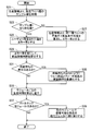
- FIG. 1st embodiment It is a perspective view showing the substrate working system of a 1st embodiment. It is a perspective view which shows the electronic component mounting apparatus which comprises the to-board work system shown in FIG. It is a top view which shows an electronic component mounting machine from the viewpoint from upper direction. It is a perspective view which shows a die supply machine. It is a block diagram of an electronic component mounting machine. It is a flowchart which shows the optimization process of the mounting order of components. It is a part of production information, and is a diagram showing the number of normal dies and defective dies of a wafer used for each production order of substrates. It is a figure which shows the number of normal dies and the number of defective dies of wafer type “A”.
- FIG. 5 is a diagram showing data related to a component supply time and before considering an error occurrence rate.
- FIG. 5 is a diagram showing data relating to a component supply time and after considering an error occurrence rate.
- FIG. 5 is a figure which shows the data after optimizing the data shown in FIG.
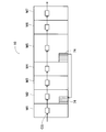
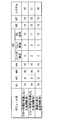
- It is a schematic diagram which shows the module lined up along a component mounting line. It is a figure for comparing the production time of each module.
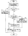
- It is a flowchart which shows the optimization process of the mounting order of the components of 2nd Embodiment.
- It shows the number of the normal die and defective die for every wafer.
- It is a flowchart which shows the optimization process of the mounting order of the components of 3rd Embodiment.
- It is a flowchart which shows the process for determining the number of remaining components of 4th Embodiment.
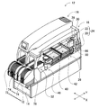
- FIG. 1 shows a substrate working system according to the first embodiment.
- An on-board work system (hereinafter, simply referred to as “system”) 10 shown in FIG. 1 performs an operation of mounting electronic components on a circuit board, and includes four electronic devices arranged adjacent to each other.
- the component mounting device 12 is configured.
- the electronic component mounting apparatus 12 has one system base 14 and two electronic component mounting machines 16 disposed adjacent to each other on the system base 14 or the width in the mounting direction of the electronic component mounting apparatus 12.
- an electronic component mounting machine 17 that is twice the electronic component mounting machine 16. That is, seven electronic component mounting machines 16 and 17 are arranged in order.
- the direction in which the electronic component mounting machines 16 and 17 are arranged is referred to as an X-axis direction
- a horizontal direction perpendicular to the direction is referred to as a Y-axis direction.
- FIG. 2 shows one electronic component mounting apparatus 12 as a representative.
- FIG. 2 is a perspective view in which a part of the exterior component of the electronic component mounting apparatus 12 is removed.
- Each of the electronic component mounting machines 16 included in the electronic component mounting apparatus 12 mainly includes a mounting unit main body 24 configured to include a frame unit 20 and a beam unit 22 overlaid on the frame unit 20, and a circuit board.
- a transport device 26 that transports in the X-axis direction and fixes it at a set position, a mounting head 28 that mounts electronic components on a circuit board fixed by the transport device 26, and a mounting head disposed on the beam unit 22
- a moving device 30 for moving 28 in the X-axis direction and the Y-axis direction, and a supply device 32 that is disposed in front of the frame portion 20 and supplies electronic components to the mounting head 28 are provided.
- the transport device 26 includes two conveyor devices 40 and 42, and the two conveyor devices 40 and 42 are parallel to each other and extend in the X-axis direction so that the central portion in the Y-axis direction of the frame portion 20. It is arranged.
- Each of the two conveyor devices 40 and 42 has a structure in which a circuit board supported by each conveyor device 40 and 42 is conveyed in the X-axis direction by an electromagnetic motor (not shown).
- each of the conveyor devices 40 and 42 has a substrate holding device (not shown), and is configured to hold the circuit board in a fixed position.
- the mounting head 28 is for mounting electronic components on the circuit board held by the transport device 26, and has a suction nozzle 50 for sucking the electronic components on the lower surface. Further, the mounting head 28 is fixed with the mark camera 44 (see FIG. 3) facing downward, and the mark camera 44 uses a reference position mark on the circuit board, an ID mark for identifying the circuit board, and an electronic component. The mounting state is imaged.
- the suction nozzle 50 communicates with a positive / negative pressure supply device 52 (see FIG. 5) via negative-pressure air and positive-pressure air passages, and sucks and holds electronic components at a negative pressure, so that a slight positive pressure is supplied. In this way, the held electronic component is detached.
- the mounting head 28 has a nozzle lifting / lowering device 54 (see FIG. 5) that lifts and lowers the suction nozzle 50 and a nozzle rotation device 55 (see FIG. 5) that rotates the suction nozzle 50 about its axis. It is possible to change the vertical position of the electronic component to be held and the holding posture of the electronic component.
- the suction nozzle 50 is attachable to and detachable from the mounting head 28, and can be changed according to the size and shape of the electronic component.
- the moving device 30 moves the mounting head 28 to an arbitrary position on the frame unit 20, an X-axis direction slide mechanism (not shown) for moving the mounting head 28 in the X-axis direction, and the mounting head 28. And a Y-axis direction slide mechanism (not shown) for moving the lens in the Y-axis direction.
- the Y-axis direction slide mechanism has a Y-axis slider 60 (see FIG. 3) provided in the beam section 22 so as to be movable in the Y-axis direction, and an electromagnetic motor 57 (see FIG. 5) as a drive source.
- the Y-axis slider 60 can be moved to an arbitrary position in the Y-axis direction by the electromagnetic motor 57.
- the X-axis direction slide mechanism includes an X-axis slider 66 provided on the Y-axis slider so as to be movable in the X-axis direction, and an electromagnetic motor 58 (see FIG. 5) as a drive source. 58, the X-axis slider 66 can be moved to an arbitrary position in the X-axis direction.
- the mounting head 28 is attached to the X-axis slider 66, so that the mounting head 28 can be moved to an arbitrary position on the frame unit 20 by the moving device 30.
- the mounting head 28 can be attached to and detached from the X-axis slider 66 with a single touch, and can be changed to a different type of work head, such as a dispenser head or an inspection head.
- a parts camera 46 is provided on the upper surface of the frame portion 20 as a base between the transport device 26 and the supply device 32 in the Y-axis direction.
- the parts camera 46 is used to capture an image when the mounting head 28 that sucks and holds the electronic component passes through the upper part and confirms the suction state based on the imaging data.
- the supply device 32 is disposed at an end portion on the front side of the frame portion 20 and is a feeder-type supply device.
- the supply device 32 includes a plurality of tape feeders 74 that house taped parts on which electronic parts are taped and wound around a reel 72, and taped parts housed in each of the plurality of tape feeders 74. And a plurality of delivery devices (not shown) that sequentially feed the electronic parts from the taped parts to the supply position to the mounting head 28.
- the tape feeder 74 is attachable to and detachable from a device pallet 76 attached to the front end portion of the frame portion 20, and can cope with replacement of electronic components.
- the device pallet 76 to / from which the tape feeder 74 is attached / detached can be attached / detached to / from the frame unit 20 by operation of a clamp mechanism (not shown) provided in the frame unit 20. Therefore, the electronic component mounting machine 16 can remove the device pallet 76 from the frame unit 20 and attach a supply device of a type different from the feeder type supply device 32 to the frame unit 20.
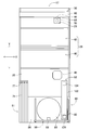
- FIG. 3 is a plan view showing the electronic component mounting machine 17 included in the electronic component mounting apparatus 12 as viewed from above.
- the width in the X-axis direction of the frame unit 20, the transport device 26, the Y-axis slider 60, and the like of the electronic component mounting machine 17 is provided in the electronic component mounting machine 16.
- the configuration is the same as that of the electronic component mounting apparatus 12 including the electronic component mounting machine 16 except that the width is about twice as large.
- the same reference numerals are used for the components of the electronic component mounting machine 17 that are common to the electronic component mounting machine 16, and the description thereof is omitted as appropriate.
- the device pallet 76 having a width of about twice is removed from the frame unit 20, and a supply device 80 of a type different from the feeder-type supply device 32 is attached to the frame unit 20.
- the supply device 80 is a mixed supply device including a tape-type supply device 81 and a wafer-type supply device 82.
- the tape-type supply device 81 includes a plurality of tape feeders 74 described above, a delivery device that sends out the electronic parts 77 formed into tapes of the tape feeders 74, and the like.
- the wafer type supply device 82 supplies the die 108 from a die assembly 106 (see FIG. 4) formed by dicing a wafer in which a dicing sheet is bonded.
- the tape-type supply device 81 and the wafer-type supply device 82 of the supply device 80 are attached to the front side of the frame unit 20 of the electronic component mounting machine 17.
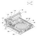
- the wafer type supply device 82 is mounted on the mounting plate 84.
- the wafer mold supply device 82 is disposed substantially at the center of the mounting plate 84 and holds the die assembly 106 fixedly, and the die assembly held by the die assembly holding device 86.
- the die assembly holding device 86 includes a pair of guide rails 100 (only one of which is shown in the figure) arranged to extend in the Y-axis direction, and the pair of guides. It has a holding frame 102 that is held by a rail 100 so as to be movable in the Y-axis direction, and a frame moving mechanism 104 that moves the holding frame 102 in the Y-axis direction.
- the die assembly holding device 86 is configured such that the die assembly 106 in which the die assembly 106 is held on the holding frame 102 is moved in the Y-axis direction by the frame moving mechanism 104.
- the pickup head 88 includes a plurality of holding rods 110 that hold suction nozzles (not shown) for sucking the die 108 at the lower end.
- the suction nozzle held by each holding rod 110 communicates with a negative pressure supply device (not shown) via an air passage, and has a structure for holding the die 108 by suction under negative pressure.
- the head moving device 90 is an XY robot type moving device, and can move the pickup head 88 to an arbitrary position on the die assembly holding device 86.
- the head moving device 90 includes a Y-axis direction slide mechanism 112 for moving the pickup head 88 in the Y-axis direction, and an X-axis direction slide mechanism 114 for moving the pickup head 88 in the X-axis direction.
- the Y-axis direction slide mechanism 112 has a Y-axis direction slider 116 provided so as to be movable in the Y-axis direction, and an electromagnetic motor (not shown) as a drive source.
- the Y-axis direction slide mechanism 112 is configured such that the Y-axis direction slider 116 can be moved to an arbitrary position in the Y-axis direction by driving an electromagnetic motor.
- the X-axis direction slide mechanism 114 has an X-axis direction slider 118 provided on the side surface of the Y-axis direction slider 116 so as to be movable in the X-axis direction, and an electromagnetic motor (not shown) as a drive source. Yes.
- the X-axis direction slide mechanism 114 is configured such that the X-axis direction slider 118 can be moved to an arbitrary position in the X-axis direction by driving an electromagnetic motor.
- the pickup head 88 is attached to the X-axis direction slider 118, so that the pickup head 88 can be moved to an arbitrary position on the die assembly holding device 86 by the head moving device 90.
- the X-axis direction slider 118 to which the pickup head 88 is attached is provided with a die camera 120 facing downward, and the X-axis direction slider 118 is moved by the head moving device 90, thereby holding the die assembly.
- the die assembly 106 held by the device 86 can be imaged at an arbitrary position. Thereby, it is possible to acquire position information and the like of each of the plurality of dies 108 of the die assembly 106.
- the shuttle mechanism 92 is fixed on the placement plate 84 on one side in the X-axis direction with respect to the die assembly holding device 86.
- the shuttle mechanism 92 includes a generally long shuttle main body 122 and a die conveyance table 124 provided on the upper surface of the shuttle main body 122.
- the die transfer table 124 is slidable in the longitudinal direction of the shuttle main body 122.
- the die transfer table 124 receives the die 108 from the pickup head 88 and transfers the received die 108 to the supply position, and has a shuttle nozzle (not shown) for receiving the die 108.
- the shuttle main body 122 is fixed to the upper surface of the mounting plate 84 at the base end portion thereof so as to extend in the Y-axis direction, and the distal end portion extends from the mounting plate 84. .
- the portion on the front end side of the shuttle mechanism 92 extends onto the frame portion 20 in a state where the supply device 80 is attached to the electronic component mounting machine 17.
- the supply device 80 is provided with a connector (not shown) that is electrically connected to the frame portion 20 of the electronic component mounting machine 17 on the lower surface of the mounting plate 84.
- the wafer type supply device 82 may include a reversing unit that receives the die 108 picked up by the pick-up head 88 and reverses it up and down as needed to supply it to the die transfer table 124.
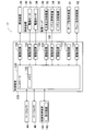
- the control device 130 of the electronic component mounting machine 17 includes a controller 132 mainly composed of a computer having a CPU, ROM, RAM, and the like, electromagnetic motors 57 and 58 of the transport device 26 and the moving device 30, A plurality of drive circuits 133 corresponding to the positive / negative pressure supply device 52, the nozzle lifting / lowering device 54, the nozzle rotation device 55, the tape type supply device 81, and the wafer type supply device 82 are provided.
- the controller 132 can control the operations of the transport device 26, the moving device 30, and the like via each drive circuit 133. Further, the controller 132 processes image data captured by the mark camera 44 and the part camera 46.
- the controller 132 processes the image data obtained by the mark camera 44 and detects information about the circuit board. Further, the controller 132 determines the holding position of the component (die 108 or electronic component 77) by the suction nozzle 50 based on the processing result of the image data obtained by the parts camera 46 and the positional information data stored in the memory 135. Detection and correction of errors, etc. are performed. In addition, the controller 132 is connected to the overall control device 141 of the system 10, and detection results and commands are transmitted to and received from the overall control device 141.
- the overall control device 141 includes a display device 143 such as a touch panel, and accepts input of various types of information or displays various types of information so that the user can confirm.
- the wafer type supply device 82 picks up the die 108 from the die assembly 106 by the pickup head 88 based on the control of the control device 130. Further, the wafer type supply device 82 can supply the die 108 to the mounting head 28 by transporting the picked up die 108 to the supply position by the shuttle mechanism 92. Specifically, first, the control device 130 controls the head moving device 90 to above the die 108 to be picked up among the plurality of dies 108 of the die assembly 106 held by the die assembly holding device 86. The die camera 120 is moved. The control device 130 images the die 108 with the die camera 120 and acquires position information of the die 108 based on the imaging data.
- the control device 130 controls the head moving device 90 based on the acquired position information of the die 108 and moves the pickup head 88 above the die 108 to be picked up.
- the control device 130 lowers the holding rod 110 of the pickup head 88.
- the suction nozzle of the holding rod 110 sucks and holds the die 108 and picks up the die 108 from the die assembly 106.
- a thrust mechanism (not shown) that pushes up the die 108 from below is provided below the die assembly holding device 86. When the die 108 is attracted by the suction nozzle, the die 108 is moved upward by the thrust mechanism. By being pushed up, the pickup of the die 108 is supported.
- the control device 130 moves the pickup head 88 that has picked up the die 108 to above the die conveyance table 124 of the shuttle mechanism 92. Further, when the die 108 is picked up by the pickup head 88, the die conveyance table 124 is set to a position on the base end side of the shuttle main body 122 (a position where the die conveyance table 124 is indicated by a solid line in FIG. 3). . Then, the control device 130 lowers the holding rod 110 of the pickup head 88 and stops the supply of negative pressure to the suction nozzle, thereby delivering the picked-up die 108 to the shuttle nozzle of the die conveyance table 124.
- the die conveyance table 124 that has received the die 108 is slid by the control device 130 from the proximal end portion of the shuttle body 122 toward the distal end portion, and the position on the distal end side of the shuttle main body 122 (the die conveyance table 124 in FIG.
- the die 108 is supplied at a position indicated by a dotted line. That is, the position indicated by the dotted line on the die carrier table 124 in FIG. 3 is the supply position of the die 108 by the wafer type supply device 82, and the die 108 supplied at that position is held by the mounting head 28.
- the control device 130 controls the tape-type supply device 81 to change the electronic component from the taped component accommodated in each of the plurality of tape feeders 74. 77 is sequentially supplied to the supply position to the mounting head 28 (the tip portion of the tape feeder 74 in FIG. 3).
- the supply device that supplies the die 108 like the wafer type supply device 82 when there is a defective die (bad die) in the die assembly 106, for example, a defective product added to the upper surface of the defective die. It is necessary to detect the mark indicating that it is based on the imaging data of the die camera 120. Further, the wafer type supply device 82 needs to search for a normal die 108 in place of the detected defective die. Therefore, in the wafer type supply device 82, the component supply time required until the normal die 108 is supplied varies depending on the number of defective dies included in the die assembly 106 on the dicing sheet. To do.
- a defective die is detected from the die assembly 106 with respect to the electronic component mounting machine 17 including the wafer type supply device 82 among the electronic component mounting machines 16 and 17.
- the error occurrence rate (hereinafter simply referred to as “error rate”) is determined, and the component supply time is corrected based on the error rate.
- the system 10 optimizes the mounting order of mounting components on the circuit board in each of the electronic component mounting machine 16 and the electronic component mounting machine 17 based on the corrected component supply time. For example, the system 10 performs the optimization process of the mounting order for every production job or every time a predetermined board is produced.
- the overall control device 141 of the system 10 determines whether or not an error rate is specified by the user before producing a substrate based on a production job, for example (step S1). For example, according to the display contents of the display device 143 of the overall control device 141, the user selects the electronic component mounting machine 17 including the wafer type supply device 82 among the electronic component mounting machines 16 and 17 connected to the component production line of the system 10. Is input using the touch panel of the display device 143.
- the error rate varies depending on the type of die 108 (wafer). Therefore, the user can set an arbitrary error rate determined based on the result of using the same type of die 108 during the operation of operating the system 10.
- step S1 determines the specified value as the error rate (step S3).
- step S1: “NO” the overall control device 141 selects a wafer of the same type (die 108) among the wafers used for the production of the past substrate. A value obtained by averaging the occurrence rates of defective dies is determined as an error rate (step S5).
- FIG. 7 shows a part of the production information, and shows the number of defective dies of the wafer used for each production order of the substrates.
- this production information may be managed collectively by the overall control device 141, or may be stored and managed in the memory 135 by the control device 130 of the electronic component mounting machine 17.
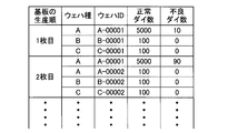
- three types of wafers “A”, “B”, and “C” are used for the production of the first substrate.
- each of the wafer types “A”, “B”, and “C” is used one by one.
- each of the wafer types “A”, “B”, and “C” includes two wafer types “A” (wafer IDs “A-00001” and “A”).
- the electronic component mounting machine 17 including the wafer type supply device 82 counts the number of normal dies and the number of defective dies for each wafer type every time a substrate is produced.
- the wafer type “A” (wafer ID “A-00001”) is 5,000 of the normal dies out of the dies 108 that the wafer mold supply device 82 has attempted to pick up. Is ten.
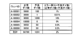
- FIG. 8 shows the number of normal dies and the number of defective dies for the wafer type “A”. For example, since the wafer ID “A-00001” has 9900 normal dies and 100 defective dies, the error rate is 1%. In addition, the wafer ID “A-00002” has 9999 normal dies and 1 defective die, and therefore has an error rate of 0.01%. Based on the production information shown in FIG. 8, the control device 130 of the electronic component mounting machine 17 determines the number of normal dies and defective dies from wafer ID “A-00001” to wafer ID “A-00006” having the same wafer type.
- the error rate of the wafer type “A” is 2%.
- the control device 130 calculates the error rate for the other wafers “B” and “C”, and transmits the error rate to the overall control device 141.
- the calculation of the error rate may be performed by the overall control device 141.
- step S6 shown in FIG. 6 the overall control device 141 determines the error rate of the wafer type to be used in the production job for the next substrate to be produced based on the error rate determined by the user input value or the production information. decide.
- the overall control device 141 notifies the determined error rate to the electronic component mounting machine 17 that uses the wafer supply device 82 in the next production job.
- the control device 130 of the electronic component mounting machine 17 calculates the component supply time based on the error rate.
- the control device 130 waits until the wafer-type supply device 82 picks up a normal die, and the wafer-type supply device 82 and other component supply devices (such as the tape-type supply device 81). ) Determines whether or not a “supply wait” that causes a delay in the operation of supplying the component has occurred (step S7).
- the control device 130 changes the supply order of the wafer type supply device 82 and other component supply devices so that the supply waiting time is shortened (step S9).
- the overall control device 141 may perform the calculation of the component supply time, whether to wait for supply, and the change of the supply order.
- FIG. 9 shows an example of the component supply order of the electronic component mounting machine 17 before optimization.
- the electronic component mounting machine 17 first supplies the die 108 of the wafer type supply device 82 as the component mounting sequence (the row of the component type in the figure is “wafer component” row) five times.
- the supply of the electronic component 77 of the tape type supply device 81 (the row of the component type in the figure is “feeder component”) is performed five times.
- FIG. 10 is a schematic diagram for explaining the mounting sequence of the electronic component mounting machine 17.
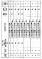
- FIG. 11 shows data relating to the component supply time stored in the memory 135 of the control device 130, and shows data before considering the error rate corresponding to the mounting sequence shown in FIG.
- the data shown in FIG. 11 includes a mounting sequence number (Seq number), a slot number, a required supply time without considering the error rate, a suction operation content, a suction operation time (operation time), whether there is a supply waiting occurrence, and a total required time. Data corresponding to each item is set.
- the electronic component mounting machine 17 is provided with a plurality of slots to which the wafer type supply device 82 and the tape type supply device 81 are connected.
- the wafer type supply device 82 is connected as an example.
- the slot number is “1”, and the slot number to which the tape supply device 81 is connected is “2”. Further, among the plurality of mounting sequences Seq, those having the same processing contents will not be described as appropriate.
- the control device 130 executes the first mounting sequence (mounting sequence Seq1), and the supply position (mounting) of the wafer type supply device 82 connected to the slot number 1
- the mounting head 28 is moved to the suction position of the head 28.
- the mounting head 28 indicates the supply position of the wafer type supply device 82 from the standby position before work, more specifically, the die transfer table 124 in FIG. Move to the part.
- the suction operation time required for the mounting head 28 to move to the suction position is, for example, 2 seconds (see the item “Suction Operation Time” in FIG. 11).
- the wafer type supply device 82 starts a process for supplying the die 108 to the supply position with the start of production.
- the required supply time required for the wafer type supply device 82 to supply the die 108 to the supply position is, for example, 2 seconds (see item “Required supply time” in FIG. 11). Since the required supply time is the same, the total required time of the mounting sequence Seq1 is 2 seconds.
- the control device 130 executes the mounting sequence Seq2 and performs the operation of mounting the die 108 supplied from the wafer type supply device 82 to the mounting head 28 on the circuit board CB.
- the control device 130 controls the mounting head 28 and sucks the die 108 at the supply position of the wafer type supply device 82 by the suction nozzle 50.
- the control device 130 causes the mounting head 28 to pass over the parts camera 46 from the supply position of the wafer type supply device 82, and is mounted by the transfer device 26 (see FIG. 3). To the mounting position of the circuit board CB fixed to the board.
- the control device 130 images the suction nozzle 50 in a state where the die 108 is sucked by the parts camera 46.
- the control device 130 corrects errors such as the holding position and posture of the die 108 sucked by the suction nozzle 50 based on the imaging data of the parts camera 46, and after correcting the error, the die 108 is placed on the circuit board with respect to the mounting head 28. Attach to CB.
- the control device 130 also moves the mounting head 28 to the supply position of the wafer type supply device 82 since the die 108 is supplied from the wafer type supply device 82 in the next mounting sequence Seq3.
- the suction operation time required for a series of operations of the mounting sequence Seq2 is, for example, 2.5 seconds.
- the required supply time of the wafer type supply device 82 is 2 seconds as in the mounting sequence Seq1. If one of the suction operation time and the supply required time is long, the next mounting sequence cannot be executed even if the operation with a short processing time is completed. For this reason, the total required time of the mounting sequence Seq2 is 2.5 seconds in accordance with the suction operation time having a long processing time.
- the control device 130 executes mounting sequences Seq3 to Seq5 for mounting the die 108 supplied from the wafer type supply device 82 on the circuit board CB.
- the operation accompanied by the mounting of the component on the circuit board CB as in the mounting sequence Seq2 depends on whether the mounting position of the component on the circuit board CB is near or far from the supply position of the component of the wafer type supply device 82. It will fluctuate. Therefore, the other attachment sequences Seq3 to Seq5 that perform the same process have different suction operation times.
- the control device 130 moves the mounting head 28 that has finished mounting the die 108 to the circuit board CB to the supply position of the tape-type supply device 81 connected to the slot number 2.
- the control device 130 executes a mounting sequence Seq7, and performs an operation of mounting the electronic component 77 supplied from the tape-type supply device 81 to the mounting head 28 on the circuit board CB.
- the mounting head 28 passes over the parts camera 46 from the supply position of the tape-type supply device 81, moves to the mounting position of the circuit board CB, and mounts the electronic component 77.
- the control device 130 repeatedly executes mounting of the electronic component 77 supplied from the tape supply device 81 on the circuit board CB in the mounting sequence Seq8 to Seq10.
- the control device 130 performs the wafer type supply device based on the error rate notified from the overall control device 141 in step S6 shown in FIG.
- the required supply time 82 is calculated.
- the control device 130 calculates the error rate and a preset coefficient by multiplying the required supply time of each mounting sequence by, for example.
- FIG. 12 shows data related to the component supply time after calculation based on the error rate.
- the required supply time of the wafer type supply apparatus 82 is 2 seconds to 2.1 seconds as a result of calculation based on the error rate at which defective dies are generated.
- the required supply time (2.1 seconds) is longer than the suction operation time (2 seconds). Therefore, the total required time of the mounting sequence Seq1 is 2.1 seconds to which the required supply time with a long processing time is applied.
- the wafer type supply device is moved until the movement of the head moving device 90 is completed. It is expected that the supply operation for transporting the die 108 picked up by 82 to the supply position will not be completed. As a result, the control device 130 causes a delay in the timing of performing the operation after the next mounting sequence Seq2. As a result of executing the correction of the required supply time based on the error rate, the control device 130 determines that the supply waiting has occurred in the mounting sequence in which the total required time is increased. In the example shown in FIG.
- the mounting sequences Seq1 and Seq3 correspond.
- the control device 130 determines that the supply waiting occurs for the mounting sequences Seq1 and Seq3 whose total required time has become longer, and sets data indicating “present” in the item “whether supply waiting has occurred”.
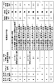
- step S9 shows data after the data related to the component supply time shown in FIG. 12 is optimized.
- the mounting sequence number before the change is referred to as an old mounting sequence
- the mounting sequence after the change is referred to as a new mounting sequence.
- control device 130 inserts, as the new mounting sequence Seq1, the old mounting sequence Seq6 for supplying the electronic component 77 from the tape supply device 81 (slot 2) before the old mounting sequence Seq1 in which supply waiting has occurred.
- the old mounting sequence Seq1 is advanced as a new mounting sequence Seq2.
- the control device 130 executes the new mounting sequence Seq1 with the start of production of the substrate, and moves the mounting head 28 to the supply position of the tape-type supply device 81 connected to the slot number 2.
- Let The suction operation time required for the mounting head 28 to move to the suction position is 2 seconds.
- the wafer type supply device 82 starts a process for supplying the die 108 to the supply position while the new mounting sequence Seq1 is executed, that is, while an operation is being performed on another supply device. It becomes possible.
- the time required for supplying the die 108 to the supply position by the wafer type supply device 82 is 2.1 seconds in consideration of the error rate, as described above.
- the wafer type supply device 82 starts the pick-up operation of the die 108 simultaneously with the start of the new mounting sequence Seq1. For this reason, the required supply time of the wafer type supply device 82 is substantially 0.1 seconds obtained by subtracting 2 seconds of the new mounting sequence Seq1 from 2.1 seconds.
- the total required time of the old mounting sequence Seq1 is shortened from 2.1 seconds before optimization to 2 seconds.
- the total required time is 2 seconds because the suction operation time of the mounting head 28 having a long processing time is applied.
- the control device 130 inserts the old mounting sequence Seq7 for supplying the electronic component 77 from the tape supply device 81 (slot 2) as the new mounting sequence Seq4 before the old mounting sequence Seq3 in which supply waiting has occurred.
- the old mounting sequence Seq3 is advanced as a new mounting sequence Seq5.
- the total required time of the new mounting sequence Seq5 (old mounting sequence Seq3) after the change is shortened from 2.1 seconds before the optimization to 2 seconds.
- the order of the mounting sequence after optimization shown in FIG. 13 is an example, and is not limited to this.
- the control device 130 uses the more accurate total required time in consideration of the delay in the required supply time of the wafer type supply device 82 due to the error rate, and the components (die 108 and electronic component 77) for the circuit board CB. It becomes possible to optimize the order of mounting.
- the control device 130 of the electronic component mounting machine 17 optimizes the total time required in consideration of the error rate. The delay can be reduced as much as possible. As a result, the system 10 can shorten the production time of the substrate and achieve the effect of production efficiency.
- each of four electronic component mounting apparatuses 12 arranged adjacent to each other includes two electronic component mounting machines 16 or one electronic component mounting machine 17.
- the overall control device 141 manages each of the plurality of electronic component mounting machines 16 and 17 as a module.
- the overall control device 141 performs optimization so that the production time (tact time) required for mounting components on the circuit board CB in each module (electronic component mounting machines 16 and 17) is shortened.
- the unit of the module set by the overall control device 141 for managing the production time can be changed as appropriate.
- the electronic component mounting device 12 may be managed as a module. In the following description, a case will be described in which the overall control device 141 executes management and optimization processing with one electronic component mounting machine 16 or electronic component mounting machine 17 as one module.
- the overall control device 141 executes step S11 after step S7 or step S9 shown in FIG.
- the overall control device 141 calculates the production time of each module (electronic component mounting machines 16, 17). For example, in the component supply time in which the mounting sequence is optimized based on the error rate shown in FIG. 13, the production time required to mount all the components (die 108 and electronic component 77) on the circuit board CB is new.
- the total required time of the mounting sequences Seq1 to Seq10 is the total time (21.5 seconds in this case).
- step S13 the overall control device 141 acquires the production time for all the modules, and determines the module having the maximum production time as the bottleneck module.
- the production time may increase as compared to before considering the error rate.
- the electronic component mounting machine 17 (module) including the wafer type supply device 82 becomes a bottleneck.
- this increase in production time means an increase compared to an ideal production time that does not include defective dies (see FIG. 11), and the order of the mounting sequence shown in FIG. 12 is not changed. It goes without saying that the production time after optimization is shortened compared to the production time as it is.
- FIG. 14 schematically shows electronic component mounting machines 16M1 to M4, M6, M7 and an electronic component mounting machine 17M5 (hereinafter, M1 to M7 are referred to as “modules”) arranged along the component mounting line of the system 10.
- M1 to M7 are referred to as “modules”.
- the system 10 reduces the production time of each of the bottleneck modules M1 to M7 when the board is produced by one component mounting line in which the modules M1 to M7 are arranged. (Throughput) can be improved.
- FIG. 15 shows the production time of each of the modules M1 to M7.
- the module M ⁇ b> 5 is the electronic component mounting machine 17 including the wafer type supply device 82. As shown in FIG.
- each of the modules M1 to M7 performs a predetermined mounting process for mounting components on the circuit board on the circuit board CB conveyed from the upstream of the component mounting line, and downstream modules M1 to M7. The operation of transporting to M7 is repeated.
- the system 10 controls the conveyance of the circuit board CB of each module M1 to M7 according to the production time of the module M1 to M7 having the longest production time, that is, the bottleneck module. To do. That is, the time required to carry out one substrate produced by the system 10 (“system production time” in FIG. 15) is the production time of the bottleneck module. Therefore, the system 10 improves the production efficiency by reducing the production time of the bottleneck modules M1 to M7.
- the module M5 changes the production time of the wafer type supply device 82 (the item “wafer part” in the figure) from 8 seconds to 9 seconds. Assume that it has increased by one second. In the modules M1 to M7 after the optimization based on the error rate is performed, the production time of the module M5 is 11 seconds, and the production times of the other modules M1 to M4, M6, and M7 are 10 seconds or less. . Therefore, the module M5 is a bottleneck module alone.
- the overall control device 141 changes the mounting condition of the module M5 (step S14). For example, the overall control device 141 changes the arrangement of the tape feeders 74 that can be mounted on the other modules M1 to M4, M6, and M7 among the plurality of tape feeders 74 mounted on the tape-type supply device 81 of the module M5. . The overall control device 141 determines the placement destination of the tape feeder 74 based on the contents of the mounting processes and the individual production times of the other modules M1 to M4, M6, and M7 other than the module M5.
- the overall control device 141 notifies the user of an instruction to move one tape feeder 74 attached to the module M5 to the module M2 having the shortest production time.
- the production time of the module M5 after changing (optimizing) a part of the arrangement of the tape feeder 74 is shortened from 11 seconds to 10 seconds.
- the production time of the module M2 is increased from 8 seconds to 9 seconds.
- the production times of the modules M1 to M7 are averaged compared with those before the optimization, and the production time of the system 10 is shortened from 11 seconds to 10 seconds.
- the overall control device 141 can improve the production efficiency by changing the arrangement of the tape feeder 74.
- the above-described changes in the mounting conditions are only examples, and are changed as appropriate.
- the system 10 may replace either of the tape feeders 74 You may optimize by changing arrangement
- the determination condition as to whether or not there is a bottleneck module of the overall control device 141 in step S13 can be appropriately set according to the configuration of the system 10 or the like. For example, as described above, the overall control apparatus 141 may determine that “there is a bottleneck module” when there is a single bottleneck module M5.
- the overall control device 141 may determine that “there is a bottleneck module” when the number of bottleneck modules among the modules M1 to M7 is equal to or less than a preset number. Further, for example, the overall control device 141 may determine that “the bottleneck module is present” when the production time of the system 10 increases before and after the processing of step S11 (recalculation of production time). Further, for example, the overall control device 141 may change the mounting conditions of the bottleneck modules M1 to M7 and determine that the production time of the system 10 can be shortened as “there is a bottleneck module”.
- the electronic component mounting machine 17 included in the system 10 includes a tape-type supply device 81 and a wafer-type supply device as a plurality of component supply units that supply components (electronic component 77 and die 108) to be mounted on the circuit board CB. 82 (see FIG. 3).
- the overall control device 141 of the system 10 uses the input value for processing (FIG. 6). (See step S3).
- the overall control device 141 averages the occurrence rate of defective dies of the same type of wafer (die 108) among the wafers used in the past production in the production information. The value is determined as an error rate (step S5). Based on the determined error rate, the system 10 determines in advance the mounting order for mounting components supplied from the tape-type supply device 81 and the wafer-type supply device 82 on the circuit board CB, or changes the determined mounting order. .
- the component supply time of each component supply device is more accurately grasped, and the order of mounting each component on the circuit board CB is optimized. This makes it possible to shorten the production time. Therefore, according to the system 10 in the present embodiment, it is possible to determine the optimal component mounting order using the more accurate component supply time of the wafer type supply device 82, and to improve the production efficiency. It becomes.
- the controller 130 of the electronic component mounting machine 17 calculates the required supply time of the wafer type supply device 82 based on the error rate (step S6), and then the wafer type supply device 82 supplies the die 108.
- the mounting sequence Seq1 in FIG. 12 it is detected that a supply waiting time that delays the operation of starting the next mounting sequence Seq2 occurs until the wafer type supply device 82 supplies a normal die.
- the control device 130 determines the order of the mounting sequences Seq1 to Seq10 for supplying components from the wafer-type supply device 82 and the tape-type supply device 81 or changes the determined order as appropriate so that the supply waiting time is shortened. .
- the control device 130 inserts an old mounting sequence Seq6 for supplying the electronic component 77 from the tape-type supply device 81 before the old mounting sequence Seq1 in which supply waiting has occurred.
- the control device 130 executes the new mounting sequence Seq1 to move the mounting head 28 to the supply position of the tape-type supply device 81, while operating the wafer-type supply device 82.
- the wafer type supply device 82 can start a process for supplying the die 108 to the supply position while the new mounting sequence Seq1 is executed, that is, while an operation for another supply device is being performed. It becomes.
- the electronic component mounting machine 17 can reduce the total required time, that is, the production time.
- the overall control device 141 manages each of the plurality of electronic component mounting machines 16 and 17 as modules.
- the overall control device 141 corrects the production time of each module according to the type of board to be produced based on the error rate (step S11).
- the overall control device 141 determines a module that becomes a bottleneck with the maximum production time among the plurality of modules based on the corrected production time (step S13).
- the overall control device 141 changes the mounting condition of the module (for example, the module M5) that has become the bottleneck (step S14).
- the overall control device 141 changes the arrangement of the tape feeders 74 that can be mounted on the other modules M1 to M4, M6, and M7 among the plurality of tape feeders 74 mounted on the tape-type supply device 81 of the module M5.
- the production times of the modules M1 to M7 are averaged compared to before the optimization, and the production time of the system 10 is shortened (see FIG. 15). As a result, the system 10 can improve the production efficiency by optimizing the arrangement of the tape feeder 74.
- FIG. 16 is a flowchart of the optimization process in the second embodiment.
- the difference from the flowchart shown in FIG. 6 of the first embodiment described above is that while the die 108 is used up to the number of switchings specified in advance by the user, the value specified by the user is set as the error rate, and the number of switchings After the die 108 is used, processing is performed using an error rate calculated based on production information.
- the description of the same content as the processing shown in the flowchart of FIG. 6 of the first embodiment is omitted as appropriate.
- the overall control device 141 acquires the number of samples of the wafer type designated from the production information (step S21 in FIG. 16). For example, the user operates the overall control device 141 to set the error rate and the number of switching for each wafer type before the system 10 starts the production of the substrate. When the user's setting operation is completed, the overall control device 141 resets the number of production information samples.
- the number of samples refers to the number of normal dies used for each wafer type and the number of defective dies attempted to be used.
- the overall control device 141 executes the processing of the flowchart shown in FIG. 16 every time the wafer type supply device 82 uses one wafer (all dies 108), for example. Note that the overall control device 141 may execute the process shown in FIG. 16 every time one board is produced or every time a predetermined number of boards are produced.
- FIG. 17 shows a part of the production information and shows the number of normal dies and the number of defective dies for each wafer ID of the wafer type “A” used in the past.
- the system 10 having a plurality of electronic component mounting machines 17 has a wafer type “A-00001”, “A-00002”,... “A-00007” in order from the upper side to the lower side in FIG. A ”wafer is used.
- the production information shown in FIG. 17 when the wafer with the wafer ID “A-00001” is used, the total number of normal dies and the number of defective dies is used, and 10,000 dies 108 are used. Accordingly, the number of samples acquired from the production information at this time is 10,000.
- step S23 the overall control device 141 compares the number of samples acquired from the production information with the number of switching designated by the user. For example, the number of switching set by the user is “50000”. The overall control device 141 does not reach the number of used dies 108, that is, the number of samples until 50,000 samples are used until all the dies 108 of the fifth wafer (wafer ID “A-00005”) are used.
- “use” includes a case where a normal die is mounted on the circuit board CB and an inspected defective die. Therefore, the overall control device 141 has fewer samples than the number of switching until all of the wafer dies 108 with the wafer ID “A-00005” are used (step S23: “YES”). Execute the process. That is, the overall control device 141 sets the value specified by the user as an error rate until the number of samples becomes larger than the number of switching, and performs optimization processing based on the error rate.
- step S23 when the overall control device 141 uses all the wafer dies 108 with the wafer ID “A-00005” and the number of samples is larger than the number of switching (step S23: “NO”), the overall control device 141 performs the processing after step S27. Execute. That is, when the number of samples is larger than the number of switching, the overall control device 141 sets a value calculated based on the production information as an error rate and performs an optimization process based on the error rate. Note that the processing contents of step S25 to step S39 after step S23 shown in FIG. 16 are the same as the processing from step S3 to step S14 shown in FIG.
- the overall control device 141 sets the value specified by the user as an error rate until the number of samples is larger than the number of switchings set by the user, and performs optimization processing based on the error rate. Further, when the number of samples increases compared to the number of switching, the overall control device 141 sets an error rate as a value calculated based on production information, and performs optimization processing based on the error rate.
- the error rate can be changed at an appropriate timing after the production information is accumulated up to a desired number of switching (number of samples) determined by the user based on the operation status and the like. It becomes possible.
- FIG. 18 is a flowchart of the optimization process in the third embodiment.
- the difference from the flowchart shown in FIG. 6 of the first embodiment described above is that, as a first point, a process using a wafer map is added.
- the second difference is that the time required to supply the die 108 is determined by the position on the wafer from which the die 108 is picked up.
- the description of the same content as the processing shown in the flowchart of FIG. 6 of the first embodiment is omitted as appropriate.
- the overall control device 141 specifies a wafer to be used in the production job of the production plan (Step S41 in FIG. 18). For example, based on the content of the production job, the overall control device 141 specifies the electronic component mounting machine 17 that mounts the die 108 on the circuit board CB when the board is produced. Then, the overall control device 141 searches the ID of the wafer to be used in the production of the substrate from the wafers held by the specified electronic component mounting machine 17. The overall control device 141 determines whether there is a wafer map corresponding to the wafer ID as a search result (step S43).
- the wafer map here is, for example, data indicating the result of inspection of non-defective products and defective products for each die 108 in the die assembly 106 in the wafer manufacturing process in accordance with the arrangement of the dies 108. is there. That is, the data indicates at which position of the die assembly 106 the defective die is arranged. Further, the overall control device 141 may perform processing for appropriately inquiring the ID of the wafer to be used to the electronic component mounting machine 17 without managing the wafer IDs held by the electronic component mounting machine 17 collectively.
- step S43 if there is a wafer map corresponding to the wafer ID to be used (step S43: “YES”), the overall control device 141 calculates an error rate based on the data of the wafer map (step S45). .
- the overall control device 141 analyzes the wafer map to detect the number of normal dies and the number of defective dies, and calculates an error rate from the detection result.
- the overall control device 141 notifies the electronic component placement machine 17 of the error rate of the calculation result.
- the control device 130 of the electronic component mounting machine 17 that has received the notification calculates the component supply time based on the error rate (step S53).
- the overall control device 141 uses an error rate (step S49) by the user or an error rate based on production information (step S51). The process using is performed. Note that the processing content of steps S47 to S53 shown in FIG. 18 is the same as the processing from step S1 to step S6 shown in FIG.
- the control device 130 determines the die 108 from which position on the wafer to pick up the die 108.
- the time required for supplying 108 is recalculated (step S55, step S57).
- the wafer type supply device 82 receives the die 108 sucked by the suction nozzle of the pickup head 88 (see FIG. 4) by the shuttle mechanism 92 (see FIG. 3) and receives a predetermined supply position. Transport to.
- the control device 130 determines the position of the die from which position of the wafer based on the number of dies 108 to be used in the production plan and the wafer (wafer ID) to be used. It is determined whether 108 is picked up. The control device 130 determines the pickup position based on the arrangement of the dies 108 on the dicing sheet, the order of picking up the dies 108 from the die assembly 106, the position of the dies 108 to start use, and the like.
- the control device 130 corrects the operation time at the time of suction based on the position of the pickup determined in step S55 (step S57). For example, the control device 130 sets a delay time that occurs in the movement of the pickup head 88 for each pickup position, and the “required supply time considering the error rate” of each of the mounting sequences Seq1 to Seq10 shown in FIG. Correct.
- the pickup position is individually specified, and the required supply time is corrected by the movement time of the pickup head 88 corresponding to the position.
- the present invention is not limited to this.
- the average value of the delay time related to the movement is set with the center of the die assembly 106 on the dicing sheet as the position of all pickups, and the processing for correcting the required supply time for each wafer is executed using the average value. May be.
- the die 108 is picked up by the pickup head 88.
- the die 108 on the dicing sheet may be directly sucked by the suction nozzle 50 of the mounting head 28.
- the time for the mounting head 28 to move to pick up the die 108 is corrected according to the position of the pickup.
- the correction processing according to the position of the component to be sucked is not limited to the wafer-type feeding device 82, but other feeding devices in which the position to suck the component is displaced, for example, electronic components regularly arranged on a tray
- the present invention may be applied to a tray-type supply device that supplies.
- control device 130 determines the waiting for supply using the required supply time corrected according to the position of the pickup (step S59). Note that the processing content of steps S59 to S67 shown in FIG. 18 is the same as the processing from step S7 to step S14 shown in FIG.
- step S43 When there is a wafer map corresponding to the ID of the wafer used for production of the substrate (step S43: “YES”), the overall control device 141 of the present embodiment is based on the data of the wafer map. Calculate the error rate. As a result, the overall control device 141 can perform processing using a more accurate error rate on a wafer for which a wafer map is available in advance.
- the control device 130 recalculates the time required to supply the die 108 depending on from which position on the wafer the die 108 is picked up (steps S55 and S57).
- the control device 130 sets a delay time that occurs in the movement of the pickup head 88 for each pickup position, and corrects the “required supply time considering the error rate” of each of the mounting sequences Seq1 to Seq10 shown in FIG. To do.
- the control device 130 can optimize the mounting order adapted to the mode of operation in which the pickup head 88 actually picks up the die 108.
- FIG. 19 is a flowchart of processing for determining the number of remaining parts in the fourth embodiment.
- the overall control device 141 and the electronic component mounting device 12 notify the user that replenishment is requested. Is common.
- the remaining number of dies 108 necessary for this processing the number of remaining normal dies excluding defective dies out of the die assembly 106 left on the dicing sheet becomes a more appropriate value. Therefore, the system 10 of the present embodiment calculates a more accurate remaining number of dies 108 using the error rate, and changes the timing for notifying the user of the supply.
- control device 130 of the electronic component mounting machine 17 determines the replenishment timing
- the processing performed by another device (such as the overall control device 141) of the control device 130 is the same, and thus the description thereof is omitted here.
- the control device 130 calculates the number of remaining parts without considering the number of defective dies. For example, at the timing when the wafer is supplied to the wafer type supply device 82, the control device 130 inquires of the overall control device 141 about the remaining number of data corresponding to the ID of the supplied wafer and receives it from the overall control device 141. The number of remaining parts data is associated with the wafer ID. Alternatively, the control device 130 searches the memory 135 (see FIG. 5) for whether or not the corresponding remaining part number data is stored. Next, the control device 130 determines whether or not there is a wafer map for the wafer for which the number of remaining parts is set (step S73). For example, the control device 130 executes processing for inquiring of the overall control device 141 for the corresponding wafer map data.
- step S73 determines whether or not the user has specified an error rate for the wafer for which the number of remaining parts is set (step S75).
- step S75 sets the specified value as the error rate (step S79).
- step S81 sets the value calculated based on the data of the same type of wafer in the production information as the error rate (step S75).
- step S83 amends the number of parts remaining using the error rate determined in step S79 or step S81 (step S83).
- the number of remaining parts after correction is expressed by the following equation.
- Number of remaining parts after correction Number of remaining parts set * (100-Error rate) If the set number of remaining parts is 1000 and the error rate is 5%, the number of remaining parts after correction is 950. Thereby, the control device 130 can set an accurate number of remaining parts in consideration of the error rate.
- step S73 If there is a corresponding wafer map (step S73: “YES”), the control device 130 analyzes the wafer map to detect normal dies, and uses the detected number of normal dies as the number of remaining parts after correction. Set (step S77). Then, for example, each time the die 108 is supplied from the wafer type supply device 82 to the mounting head 28 during the production of the substrate, the control device 130 subtracts and subtracts the set number of remaining parts after correction. When the later value reaches a preset threshold value, the user is notified of wafer replenishment.
- the control device 130 corrects the remaining number of parts of the wafer die 108 provided to the wafer type supply device 82 (step S83). Then, the control device 130 determines the timing for supplying the wafer to the wafer type supply device 82 using the corrected number of remaining parts. As a result, since the control device 130 corrects the remaining number of parts using the error rate, the more accurate remaining part number obtained by removing the number of defective dies from the preset remaining part number can be used for processing. . Therefore, since the control device 130 determines the remaining number of parts using a more accurate value, it is possible to notify the user of wafer replenishment to the wafer type supply device 82 at a more appropriate timing.
- the timing for calculating the error rate in each of the above embodiments is an example, and can be changed as appropriate.
- the overall control device 141 compares the number of parts (number of samples) used for production with the number of switching preset by the user, and calculates the error rate from the production information. Although it determined, it is not limited to this.
- the overall control device 141 may calculate the error rate when the number of boards to be produced in advance is set as the number of switching by the user and the production is completed by the number of boards.
- the overall control device 141 may be configured to set the timing at which a predetermined time has elapsed from the start of substrate production as the error rate calculation timing.
- the control device 130 causes the image of the parts camera 46 when the suction position is largely deviated in the suction operation of the die 108 by the suction nozzle 50 of the mounting head 28.
- the die 108 cannot be mounted from the data and the sucked die 108 is discarded.
- the mounting head 28 needs to pick up the die 108 again.
- the mounting sequence is switched to optimize the configuration. Also good. According to such a system 10, it is possible to deal with the optimization by processing even when the supply waiting occurs due to the discarding operation.
- the electronic component mounting machine 17 having a width twice as large in the X direction as the electronic component mounting machine 16 includes the wafer type supply device 82 and the tape type supply device 81.
- the machine 16 may include a wafer type supply device 82 and a tape type supply device 81.
- the electronic component mounting device 12 and the electronic component mounting machines 16 and 17 are other types of supply devices such as a tape-type supply device 81 and a wafer-type supply device 82, for example, a tray-type supply device. You may prepare.
- the system 10 preferably optimizes the mounting order including the tray-type supply device.
- the electronic component mounting machine 17 may implement the optimization of the mounting order in the several wafer type supply apparatus 82 as a structure provided with the several wafer type supply apparatus 82.
- the die 108 sucked by the suction nozzle of the pickup head 88 of the wafer type supply device 82 is received by the shuttle mechanism 92 and transferred to a predetermined supply position, and this supply is performed.
- the position is configured to be delivered to the suction nozzle 50 of the mounting head 28, but is not limited to this configuration.
- the suction head of the pickup head 88 of the wafer type supply device 82 may be turned upside down so that the die 108 faces upward and is delivered to the suction nozzle 50 of the mounting head 28.
- the die 108 on the dicing sheet may be directly sucked by the suction nozzle 50 of the mounting head 28.
- the mounting head 28 functions as a part of the die supply unit in the present application.
- the overall control device 141 and the control device 130 of the electronic component mounting machine 17 are examples of a control unit.
- the wafer type supply device 82 is an example of a die supply unit.
- the die 108 and the electronic component 77 are examples of components.
- the tape-type supply device 81 is an example of a component supply unit.
- the time for accumulating past production information in the first embodiment or the production information accumulation time according to the number of switching in the second embodiment is an example of a predetermined period during the production of the circuit board.
- the value input by the user is an example of data related to a defective die included in the wafer.
Landscapes
- Engineering & Computer Science (AREA)
- Manufacturing & Machinery (AREA)
- Microelectronics & Electronic Packaging (AREA)
- Operations Research (AREA)
- Supply And Installment Of Electrical Components (AREA)
- Die Bonding (AREA)
Abstract
Description
以下、本発明を具体化した一実施形態について図面を参照して説明する。
図1は、第1実施形態の対基板作業システムを示している。図1に示す対基板作業システム(以下、単に「システム」という場合がある)10は、回路基板に電子部品を装着する作業を行うものであり、互いに隣接して配設された4台の電子部品装着装置12から構成されている。電子部品装着装置12は、1つのシステムベース14と、そのシステムベース14の上に互いに隣接されて配設された2つの電子部品装着機16、又は電子部品装着装置12の配設方向における幅が電子部品装着機16の2倍である電子部品装着機17とを含んで構成されている。つまり、7台の電子部品装着機16,17が順に並んで配列されている。なお、以下の説明において、電子部品装着機16,17の並ぶ方向をX軸方向とし、その方向に直角な水平の方向をY軸方向と称する。
図6に示すフローチャートは、部品の装着順の最適化処理の内容を示している。
まず、システム10の統括制御装置141は、例えば生産ジョブに基づいて基板を生産する前に、ユーザからエラー率の指定があるか否かを判定する(ステップS1)。例えば、ユーザは、統括制御装置141の表示装置143の表示内容に従って、システム10の部品生産ラインに接続された電子部品装着機16,17のうち、ウェハ型供給装置82を備える電子部品装着機17のエラー率を表示装置143のタッチパネルを使って入力する。エラー率は、ダイ108(ウェハ)の種類などによって異なる。このため、ユーザは、システム10を稼働させる運用の中で、同一の種類のダイ108を使用した結果などに基づいて決定した任意のエラー率を設定することが可能となっている。
次に、図6に示すステップS6において、統括制御装置141は、ユーザの入力値又は生産情報によって決定したエラー率に基づいて、次に生産する基板の生産ジョブで使用するウェハ種のエラー率を決定する。統括制御装置141は、次の生産ジョブでウェハ型供給装置82を使用する電子部品装着機17に対して決定したエラー率を通知する。通知を受けた電子部品装着機17の制御装置130は、エラー率に基づいて部品供給時間を演算する。
次に、システム10の統括制御装置141は、モジュールごとの最適化を実施する。図1に示すように、システム10は、互いに隣接して配列された4台の電子部品装着装置12の各々が2台の電子部品装着機16、又は1台の電子部品装着機17を備える。統括制御装置141は、例えば、この複数の電子部品装着機16,17の各々をモジュールとして管理する。そして、統括制御装置141は、各モジュール(電子部品装着機16,17)において回路基板CBに部品を装着する際に必要となる生産時間(タクトタイム)が短縮されるように最適化を行う。なお、統括制御装置141が生産時間を管理するために設定するモジュールの単位は、適宜変更可能であり、例えば、電子部品装着装置12をモジュールとして管理してもよい。以下の説明では、統括制御装置141が1台の電子部品装着機16又は電子部品装着機17を1つのモジュールとして管理及び最適化の処理を実行する場合について説明する。
<効果1>システム10が備える電子部品装着機17は、回路基板CBに装着する部品(電子部品77及びダイ108)を供給する複数の部品供給部として、テープ型供給装置81及びウェハ型供給装置82を備える(図3参照)。システム10の統括制御装置141は、ウェハ型供給装置82が備えるウェハ内に含まれる不良ダイの数を示すエラー率をユーザが入力した場合には、入力された値を処理に用いる(図6のステップS3参照)。また、統括制御装置141は、ユーザからの入力がない場合に、生産情報内の過去の生産に使用したウェハのうち、同一の種類のウェハ(ダイ108)の不良ダイの発生率を平均化した値をエラー率として決定する(ステップS5)。システム10は、決定されたエラー率に基づいてテープ型供給装置81やウェハ型供給装置82から供給される部品を回路基板CBに装着する装着順を予め決定、あるいは決定後の装着順を変更する。
次に、本発明を具体化した第2実施形態について説明する。図16は、第2実施形態のおける最適化する処理のフローチャートである。上記した第1実施形態の図6に示すフローチャートとの相違点は、予めユーザにより指定された切り替え数までダイ108を使用する間は、ユーザによって指定された値をエラー率として設定し、切り替え数までダイ108を使用した後は、生産情報に基づいて算出されたエラー率を用いて処理する点が異なる。なお、以下の説明では、第1実施形態の図6のフローチャートで示した処理と同様の内容については、その説明を適宜省略する。
<効果>統括制御装置141は、ユーザによって設定された切り替え数に比べてサンプル数が多くなるまで、ユーザによって指定された値をエラー率とし、そのエラー率に基づいて最適化の処理を行う。また、統括制御装置141は、サンプル数が切り替え数に比べて多くなると、生産情報に基づいて算出される値をエラー率とし、そのエラー率に基づいて最適化の処理を行う。これにより、当該統括制御装置141によれば、ユーザが運用状況などに基づいて判断した所望の切り替え数(サンプル数)まで生産情報を蓄積した上で、適切なタイミングでエラー率を変更することが可能となる。
次に、本発明を具体化した第3実施形態について説明する。図18は、第3実施形態のおける最適化する処理のフローチャートである。上記した第1実施形態の図6に示すフローチャートとの相違点は、1点目として、ウェハマップを用いた処理が追加されている点が異なる。また、2点目の相違点は、ウェハのどの位置からダイ108をピックアップするかによってダイ108を供給するために必要となる時間を決定する点である。なお、以下の説明では、第1実施形態の図6のフローチャートで示した処理と同様の内容については、その説明を適宜省略する。
<効果1>本実施形態の統括制御装置141は、基板の生産に使用するウェハのIDに対応するウェハマップがある場合には(ステップS43:「YES」)、そのウェハマップのデータに基づいてエラー率を演算する。これにより、統括制御装置141は、予めウェハマップが入手可能なウェハに対して、より正確なエラー率を用いた処理が可能となる。
次に、本発明を具体化した第4実施形態について説明する。図19は、第4実施形態のおける部品残数を決定するための処理のフローチャートである。統括制御装置141や電子部品装着装置12は、ウェハ型供給装置82の各々に供されるウェハのダイ108の残数が少なくなってくると、ユーザに補給を要請する旨の通知などを行うのが一般的である。この処理に必要となるダイ108の残数は、ダイシングシート上に残されたダイ集合体106のうち、不良ダイを除いた残りの正常ダイ数がより適切な値となる。そこで、本実施形態のシステム10は、エラー率を用いてより正確なダイ108の残数を演算し、ユーザに補給を通知するタイミングを変更する。以下の説明では、一例として、電子部品装着機17の制御装置130が、補給のタイミングを決定する場合について説明する。なお、制御装置130の他の装置(統括制御装置141など)が実施する場合については、同様の処理となるため、ここでの説明は省略する。
補正後の部品残数=設定済みの部品残数*(100-エラー率)
設定済みの部品残数が1000個、エラー率を5%とすると、補正後の部品残数は950個となる。これにより、制御装置130は、エラー率を考慮した正確な部品残数を設定することが可能となる。
<効果1>制御装置130は、エラー率に基づいて、ウェハ型供給装置82に供されるウェハのダイ108の部品残数を補正する(ステップS83)。そして、制御装置130は、補正した部品残数を用いてウェハをウェハ型供給装置82に補給するタイミングを決定する。これにより、制御装置130は、エラー率を用いて部品残数を補正するため、予め設定された部品残数の中から不良ダイの数を除いたより正確な部品残数を処理に用いることができる。従って、制御装置130は、より正確な値を用いて部品残数を判定するため、ユーザに対してより適切なタイミングでウェハ型供給装置82に対するウェハの補給を通知することが可能となる。
例えば、上記各実施形態におけるエラー率を演算するタイミングは、一例であり、適宜変更できる。例えば、上記第2実施形態において、統括制御装置141は、生産に使用した部品数(サンプル数)と、ユーザによって予め設定された切り替え数と比較して、生産情報からエラー率を算出するタイミングを判定したが、これに限定されない。例えば、統括制御装置141は、ユーザによって予め生産する基板の枚数が切り替え数として設定され、その基板の枚数だけ生産が完了した時点でエラー率を算出してもよい。あるいは、統括制御装置141は、基板の生産の開始から所定の時間経過したタイミングを、エラー率の算出のタイミングとして設定する構成でもよい。
また、上記各実施形態において、電子部品装着装置12及び電子部品装着機16,17は、テープ型供給装置81及びウェハ型供給装置82の他の種類の供給装置、例えば、トレイ型の供給装置を備えてもよい。この場合、システム10は、トレイ型の供給装置を含めて装着順の最適化を実施することが好ましい。
また、上記各実施形態において、電子部品装着機17は、複数のウェハ型供給装置82を備える構成として、複数のウェハ型供給装置82における装着順の最適化を実施してもよい。
Claims (7)
- 回路基板に装着する部品を供給する複数の部品供給部と、
前記複数の部品供給部のうちの1つであって、ダイシングされたウェハからダイを供給するダイ供給部と、
複数の前記回路基板の生産中の所定期間内に前記ダイ供給部が供給を試みた不良ダイの数、及び前記ウェハに含まれる不良ダイに係るデータの少なくとも一方に基づいて決定されるエラー発生率に基づいて、前記ダイを含む前記部品を前記回路基板に装着する装着順を決定又は変更する制御部と、
を備えることを特徴とする対基板作業システム。 - 前記制御部は、前記ダイ供給部が前記ダイを供給する装着シーケンスにおいて、前記ダイ供給部が正常なダイを供給するまでの間、次の装着シーケンスを開始する動作が遅延する供給待ち時間が短縮されるように、前記ダイ供給部を含む前記複数の部品供給部の供給の順番を決定又は変更することを特徴とする請求項1に記載の対基板作業システム。
- 前記制御部は、前記部品供給部から供給された前記部品を前記回路基板に装着する複数のモジュールの各々の生産時間を管理し、生産する部品実装回路基板の種類に応じた前記複数のモジュールの各々の生産時間を前記エラー発生率に基づいて補正し、補正後の前記生産時間に基づいて前記複数のモジュールのうち、ボトルネックとなるモジュールを判定し、判定結果に基づいて前記複数のモジュールの各々において供給する前記部品の種類を変更することを特徴とする請求項1又は請求項2に記載の対基板作業システム。
- 前記不良ダイに係るデータは、前記不良ダイの前記ウェハにおける位置を示すウェハマップであり、
前記制御部は、前記ウェハマップに基づいて前記エラー発生率を決定することを特徴とする請求項1乃至請求項3のいずれかに記載の対基板作業システム。 - 前記制御部は、前記ウェハにおける前記ダイをピックアップする位置に応じて、前記ダイを供給するために必要となる時間を決定することを特徴とする請求項1乃至請求項4のいずれかに記載の対基板作業システム。
- 前記制御部は、前記エラー発生率に基づいて、前記ダイ供給部に供される前記ウェハの前記ダイの残数を演算し、演算結果に基づいて前記ウェハを前記ダイ供給部に補給するタイミングを決定することを特徴とする請求項1乃至請求項5のいずれかに記載の対基板作業システム。
- 回路基板に装着する部品を供給する複数の部品供給部と、前記複数の部品供給部のうちの1つであって、ダイシングされたウェハからダイを供給するダイ供給部と、を備える対基板作業システムの部品の装着順を管理する方法であって、
複数の前記回路基板の生産中の所定期間内に前記ダイ供給部が供給を試みた不良ダイの数、及び前記ウェハに含まれる不良ダイに係るデータの少なくとも一方に基づいて決定されるエラー発生率に基づいて、前記ダイを含む部品を前記回路基板に装着する装着順を決定又は変更することを特徴とする対基板作業システムの部品の装着順を管理する方法。
Priority Applications (5)
| Application Number | Priority Date | Filing Date | Title |
|---|---|---|---|
| CN201480075741.4A CN106030769B (zh) | 2014-02-19 | 2014-02-19 | 对基板作业系统及管理对基板作业系统的元件的安装顺序的方法 |
| PCT/JP2014/053884 WO2015125226A1 (ja) | 2014-02-19 | 2014-02-19 | 対基板作業システム及び対基板作業システムの部品の装着順を管理する方法 |
| JP2016503817A JP6319818B2 (ja) | 2014-02-19 | 2014-02-19 | 対基板作業システム及び対基板作業システムの部品の装着順を管理する方法 |
| US15/119,082 US10375870B2 (en) | 2014-02-19 | 2014-02-19 | Board work system, and method for managing mounting order of components in board work system |
| EP14883494.8A EP3109896B1 (en) | 2014-02-19 | 2014-02-19 | Substrate working system and method for managing order in which components are mounted by substrate working system |
Applications Claiming Priority (1)
| Application Number | Priority Date | Filing Date | Title |
|---|---|---|---|
| PCT/JP2014/053884 WO2015125226A1 (ja) | 2014-02-19 | 2014-02-19 | 対基板作業システム及び対基板作業システムの部品の装着順を管理する方法 |
Publications (1)
| Publication Number | Publication Date |
|---|---|
| WO2015125226A1 true WO2015125226A1 (ja) | 2015-08-27 |
Family
ID=53877764
Family Applications (1)
| Application Number | Title | Priority Date | Filing Date |
|---|---|---|---|
| PCT/JP2014/053884 Ceased WO2015125226A1 (ja) | 2014-02-19 | 2014-02-19 | 対基板作業システム及び対基板作業システムの部品の装着順を管理する方法 |
Country Status (5)
| Country | Link |
|---|---|
| US (1) | US10375870B2 (ja) |
| EP (1) | EP3109896B1 (ja) |
| JP (1) | JP6319818B2 (ja) |
| CN (1) | CN106030769B (ja) |
| WO (1) | WO2015125226A1 (ja) |
Cited By (2)
| Publication number | Priority date | Publication date | Assignee | Title |
|---|---|---|---|---|
| US20190049935A1 (en) * | 2016-04-26 | 2019-02-14 | Fujitsu Limited | Production plan generation device, production plan generation method, and production plan |
| CN111433898A (zh) * | 2017-12-07 | 2020-07-17 | 株式会社富士 | 信息管理装置及信息管理方法 |
Families Citing this family (13)
| Publication number | Priority date | Publication date | Assignee | Title |
|---|---|---|---|---|
| WO2015162700A1 (ja) * | 2014-04-22 | 2015-10-29 | 富士機械製造株式会社 | 荷重測定方法および、回収方法 |
| WO2016038730A1 (ja) * | 2014-09-12 | 2016-03-17 | 富士機械製造株式会社 | 対基板作業装置及び対基板作業システム |
| WO2018179429A1 (ja) * | 2017-03-31 | 2018-10-04 | 株式会社Fuji | 対基板作業機 |
| EP3616482B1 (de) * | 2017-07-11 | 2023-03-22 | Siemens Aktiengesellschaft | Verfahren und steuerungseinrichtung zur durchlaufzeitoptimierten produktion von leiterplatten auf einer bestückungslinie |
| EP3709783B1 (en) * | 2017-11-06 | 2022-10-12 | Fuji Corporation | Component mounting line |
| JP7142463B2 (ja) * | 2018-05-15 | 2022-09-27 | Juki株式会社 | 生産システム、実装装置、生産方法 |
| CN112136373B (zh) * | 2018-05-30 | 2021-10-22 | 雅马哈发动机株式会社 | 元件补给管理系统和元件安装系统 |
| EP3806599B1 (en) * | 2018-05-31 | 2025-07-23 | Fuji Corporation | Determination device and component mounting apparatus having same |
| WO2020003385A1 (ja) * | 2018-06-26 | 2020-01-02 | 株式会社Fuji | 実装機および実装システム |
| KR102267919B1 (ko) | 2018-06-28 | 2021-06-23 | 주식회사 고영테크놀러지 | 기판에 실장된 부품의 실장 불량 원인을 결정하는 전자 장치 및 방법 |
| WO2020111756A1 (ko) * | 2018-11-27 | 2020-06-04 | 주식회사 고영테크놀러지 | 기판에 대한 검사 결과를 표시하는 전자 장치 및 방법 |
| WO2022113255A1 (ja) * | 2020-11-27 | 2022-06-02 | 株式会社Fuji | 基板生産シミュレーション方法 |
| WO2022213207A1 (en) * | 2021-04-07 | 2022-10-13 | Addem Labs Inc. | System and method for assembly and/or modification of printed circuit boards (pcbs) |
Citations (2)
| Publication number | Priority date | Publication date | Assignee | Title |
|---|---|---|---|---|
| JPH0992664A (ja) * | 1995-09-22 | 1997-04-04 | Matsushita Electric Ind Co Ltd | チップの搭載装置 |
| JP2003289200A (ja) * | 2002-03-28 | 2003-10-10 | Matsushita Electric Ind Co Ltd | 部品実装方法、部品実装機および実装順序決定プログラム |
Family Cites Families (8)
| Publication number | Priority date | Publication date | Assignee | Title |
|---|---|---|---|---|
| WO2000016602A1 (en) * | 1998-09-10 | 2000-03-23 | Matsushita Technology (S) Pte Ltd | A method of supplying components to an electronic component mounting or insertion machine |
| KR100366320B1 (ko) * | 1998-09-17 | 2002-12-31 | 마츠시타 덴끼 산교 가부시키가이샤 | 부품 공급 방법, 부품 공급 장치, 부품 실장 방법 및 부품실장 장치 |
| DE19963832A1 (de) * | 1999-12-30 | 2001-07-05 | Ericsson Telefon Ab L M | Programmprofilierung |
| CN100369536C (zh) | 2001-03-14 | 2008-02-13 | 莱格西电子股份有限公司 | 制造具有三维半导体芯片阵列安装面的电路板的方法和装置 |
| JP4093854B2 (ja) | 2002-04-05 | 2008-06-04 | 松下電器産業株式会社 | 電子部品実装装置 |
| JP4390503B2 (ja) * | 2003-08-27 | 2009-12-24 | パナソニック株式会社 | 部品実装装置及び部品実装方法 |
| JP5103238B2 (ja) | 2008-03-25 | 2012-12-19 | 株式会社日立ハイテクインスツルメンツ | 電子部品装着装置 |
| JP5898446B2 (ja) | 2011-10-03 | 2016-04-06 | 富士機械製造株式会社 | ダイ供給機 |
-
2014
- 2014-02-19 WO PCT/JP2014/053884 patent/WO2015125226A1/ja not_active Ceased
- 2014-02-19 JP JP2016503817A patent/JP6319818B2/ja not_active Expired - Fee Related
- 2014-02-19 US US15/119,082 patent/US10375870B2/en active Active
- 2014-02-19 CN CN201480075741.4A patent/CN106030769B/zh active Active
- 2014-02-19 EP EP14883494.8A patent/EP3109896B1/en active Active
Patent Citations (2)
| Publication number | Priority date | Publication date | Assignee | Title |
|---|---|---|---|---|
| JPH0992664A (ja) * | 1995-09-22 | 1997-04-04 | Matsushita Electric Ind Co Ltd | チップの搭載装置 |
| JP2003289200A (ja) * | 2002-03-28 | 2003-10-10 | Matsushita Electric Ind Co Ltd | 部品実装方法、部品実装機および実装順序決定プログラム |
Cited By (4)
| Publication number | Priority date | Publication date | Assignee | Title |
|---|---|---|---|---|
| US20190049935A1 (en) * | 2016-04-26 | 2019-02-14 | Fujitsu Limited | Production plan generation device, production plan generation method, and production plan |
| US10921791B2 (en) * | 2016-04-26 | 2021-02-16 | Fujitsu Limited | Production plan generation device, production plan generation method, and production plan |
| CN111433898A (zh) * | 2017-12-07 | 2020-07-17 | 株式会社富士 | 信息管理装置及信息管理方法 |
| CN111433898B (zh) * | 2017-12-07 | 2023-06-23 | 株式会社富士 | 信息管理装置及信息管理方法 |
Also Published As
| Publication number | Publication date |
|---|---|
| US20160360657A1 (en) | 2016-12-08 |
| JP6319818B2 (ja) | 2018-05-09 |
| US10375870B2 (en) | 2019-08-06 |
| CN106030769A (zh) | 2016-10-12 |
| CN106030769B (zh) | 2019-07-12 |
| JPWO2015125226A1 (ja) | 2017-03-30 |
| EP3109896B1 (en) | 2019-03-27 |
| EP3109896A1 (en) | 2016-12-28 |
| EP3109896A4 (en) | 2017-05-03 |
Similar Documents
| Publication | Publication Date | Title |
|---|---|---|
| JP6319818B2 (ja) | 対基板作業システム及び対基板作業システムの部品の装着順を管理する方法 | |
| CN111447823B (zh) | 更换控制装置 | |
| CN112166660B (zh) | 元件安装系统以及元件供给单元的配置指示方法 | |
| WO2020039495A1 (ja) | 部品実装システム | |
| US20170347506A1 (en) | Component mounting machine | |
| US12550309B2 (en) | Component mounting system | |
| KR20160013840A (ko) | 기판 작업 장치, 기판 작업 방법 및 기판 작업 시스템 | |
| US10863657B2 (en) | Electronic component mounting method | |
| WO2004064473A1 (ja) | 実装ラインにおける基板搬入方法、基板生産システムおよび基板生産システムにおける基板生産方法 | |
| CN105960834A (zh) | 电子元件安装装置 | |
| JP6545029B2 (ja) | 対基板作業システム | |
| JP2010109291A (ja) | 電子部品の装着方法、電子部品装着装置及び電子部品装着装置の電子部品装着順序決定方法 | |
| WO2016181439A1 (ja) | 実装装置及び実装方法 | |
| JP6204995B2 (ja) | 対基板作業装置 | |
| JP5533550B2 (ja) | 部品実装装置及び部品実装方法 | |
| CN108012521B (zh) | 部件安装方法 | |
| US20240373612A1 (en) | Management device, mounting system, and production method | |
| JP2024040656A (ja) | 部品実装システムおよび部品実装方法 | |
| WO2023149055A1 (ja) | 部品装着装置 | |
| WO2025238851A1 (ja) | 部品実装システム | |
| JP6760790B2 (ja) | 表面実装機 | |
| JP2023112279A (ja) | 生産装置およびデータ管理方法 | |
| JP6353371B2 (ja) | 表面実装機及び部品の実装方法 | |
| CN113950874A (zh) | 元件安装机 |
Legal Events
| Date | Code | Title | Description |
|---|---|---|---|
| 121 | Ep: the epo has been informed by wipo that ep was designated in this application |
Ref document number: 14883494 Country of ref document: EP Kind code of ref document: A1 |
|
| ENP | Entry into the national phase |
Ref document number: 2016503817 Country of ref document: JP Kind code of ref document: A |
|
| REEP | Request for entry into the european phase |
Ref document number: 2014883494 Country of ref document: EP |
|
| WWE | Wipo information: entry into national phase |
Ref document number: 2014883494 Country of ref document: EP |
|
| WWE | Wipo information: entry into national phase |
Ref document number: 15119082 Country of ref document: US |
|
| NENP | Non-entry into the national phase |
Ref country code: DE |