WO2015133294A1 - 防止装置 - Google Patents
防止装置 Download PDFInfo
- Publication number
- WO2015133294A1 WO2015133294A1 PCT/JP2015/054736 JP2015054736W WO2015133294A1 WO 2015133294 A1 WO2015133294 A1 WO 2015133294A1 JP 2015054736 W JP2015054736 W JP 2015054736W WO 2015133294 A1 WO2015133294 A1 WO 2015133294A1
- Authority
- WO
- WIPO (PCT)
- Prior art keywords
- resistor
- current
- value
- switch
- potential
- Prior art date
- Legal status (The legal status is an assumption and is not a legal conclusion. Google has not performed a legal analysis and makes no representation as to the accuracy of the status listed.)
- Ceased
Links
Images

Classifications
-
- H—ELECTRICITY
- H02—GENERATION; CONVERSION OR DISTRIBUTION OF ELECTRIC POWER
- H02H—EMERGENCY PROTECTIVE CIRCUIT ARRANGEMENTS
- H02H3/00—Emergency protective circuit arrangements for automatic disconnection directly responsive to an undesired change from normal electric working condition with or without subsequent reconnection ; integrated protection
- H02H3/08—Emergency protective circuit arrangements for automatic disconnection directly responsive to an undesired change from normal electric working condition with or without subsequent reconnection ; integrated protection responsive to excess current
- H02H3/10—Emergency protective circuit arrangements for automatic disconnection directly responsive to an undesired change from normal electric working condition with or without subsequent reconnection ; integrated protection responsive to excess current additionally responsive to some other abnormal electrical conditions
-
- H—ELECTRICITY
- H02—GENERATION; CONVERSION OR DISTRIBUTION OF ELECTRIC POWER
- H02H—EMERGENCY PROTECTIVE CIRCUIT ARRANGEMENTS
- H02H1/00—Details of emergency protective circuit arrangements
- H02H1/0007—Details of emergency protective circuit arrangements concerning the detecting means
-
- H—ELECTRICITY
- H02—GENERATION; CONVERSION OR DISTRIBUTION OF ELECTRIC POWER
- H02H—EMERGENCY PROTECTIVE CIRCUIT ARRANGEMENTS
- H02H3/00—Emergency protective circuit arrangements for automatic disconnection directly responsive to an undesired change from normal electric working condition with or without subsequent reconnection ; integrated protection
- H02H3/006—Calibration or setting of parameters
-
- H—ELECTRICITY
- H02—GENERATION; CONVERSION OR DISTRIBUTION OF ELECTRIC POWER
- H02H—EMERGENCY PROTECTIVE CIRCUIT ARRANGEMENTS
- H02H3/00—Emergency protective circuit arrangements for automatic disconnection directly responsive to an undesired change from normal electric working condition with or without subsequent reconnection ; integrated protection
- H02H3/08—Emergency protective circuit arrangements for automatic disconnection directly responsive to an undesired change from normal electric working condition with or without subsequent reconnection ; integrated protection responsive to excess current
- H02H3/085—Emergency protective circuit arrangements for automatic disconnection directly responsive to an undesired change from normal electric working condition with or without subsequent reconnection ; integrated protection responsive to excess current making use of a thermal sensor, e.g. thermistor, heated by the excess current
-
- H—ELECTRICITY
- H02—GENERATION; CONVERSION OR DISTRIBUTION OF ELECTRIC POWER
- H02H—EMERGENCY PROTECTIVE CIRCUIT ARRANGEMENTS
- H02H3/00—Emergency protective circuit arrangements for automatic disconnection directly responsive to an undesired change from normal electric working condition with or without subsequent reconnection ; integrated protection
- H02H3/08—Emergency protective circuit arrangements for automatic disconnection directly responsive to an undesired change from normal electric working condition with or without subsequent reconnection ; integrated protection responsive to excess current
- H02H3/087—Emergency protective circuit arrangements for automatic disconnection directly responsive to an undesired change from normal electric working condition with or without subsequent reconnection ; integrated protection responsive to excess current for DC applications
-
- H—ELECTRICITY
- H03—ELECTRONIC CIRCUITRY
- H03K—PULSE TECHNIQUE
- H03K17/00—Electronic switching or gating, i.e. not by contact-making and –breaking
- H03K17/08—Modifications for protecting switching circuit against overcurrent or overvoltage
- H03K17/082—Modifications for protecting switching circuit against overcurrent or overvoltage by feedback from the output to the control circuit
- H03K17/0822—Modifications for protecting switching circuit against overcurrent or overvoltage by feedback from the output to the control circuit in field-effect transistor switches
Definitions
- the present invention relates to a prevention device for preventing an overcurrent from flowing in a current path.
- the vehicle is equipped with a power supply system that supplies power to the electrical equipment from the power supply.
- a power supply system that supplies power to the electrical equipment from the power supply.
- the power supply system is equipped with a prevention device (see, for example, Patent Document 1) that prevents an overcurrent from flowing in the current path from the power supply to the electrical device.
- a prevention device in which a switch is provided in a current path from a power source to a load, and the potential at one end on the load side of the switch is compared with a threshold potential.
- the switch is a semiconductor switch
- the potential at one end on the load side of the switch greatly decreases due to a voltage drop at the on-resistance of the switch.
- the switch when the potential at one end on the load side of the switch becomes lower than the threshold potential, the switch is turned off. This prevents overcurrent from flowing in the current path.
- the temperature in the power supply system changes according to the environment in which the vehicle is traveling or the operating condition of the load.
- the value of the current allowed to flow through the switch varies depending on the temperature around the switch.
- the switch may fail even when the value of the current flowing through the switch is relatively small. Therefore, in the above-described prevention device, when the threshold potential is set to a constant value, there is a possibility that an overcurrent exceeding the current value allowed to flow through the switch flows in the current path.
- the prevention devices described above are manufactured in large quantities, the on-resistance values of the switches vary greatly. For this reason, when the threshold potential is the same for all the prevention devices, the prevention device with a small switch on-resistance value has a current path even if the potential at one end on the load side of the switch is higher than the threshold potential. There is a possibility that an overcurrent flows.
- the present invention has been made in view of such circumstances, and an object thereof is to provide a prevention device that can reliably prevent an overcurrent from flowing in a current path.
- the prevention device includes a switch provided in a current path, and in the prevention device that prevents an overcurrent from flowing in the current path by turning off the switch, one end is connected to one end of the switch
- a comparison unit that compares the potential at the other end, and the result of the comparison performed by the comparison unit indicates that the potential at the other end of the switch is lower than the potential at the other end of the resistor. It is configured to be turned off.
- a power source is connected to one end of the switch, and a load is connected to the other end of the switch, and a current flows in a current path from the power source to the load.
- One end of the resistor is connected to one end of the switch, and the constant current circuit allows a constant current to flow from one end side of the resistor to the other end side. Then, the potentials at the other ends of the switches and the resistors are compared.
- the potential at the other end of the switch is a value obtained by subtracting the voltage across the switch from the output voltage of the power source, and the potential at the other end of the resistor is derived from the output voltage of the power source across the resistor. The value obtained by subtracting the voltage between them. Since a constant current flows through the resistor by the constant current circuit, the voltage across the resistor is constant. When a current of a predetermined value or more flows in the current path and the voltage across the switch becomes equal to or higher than the predetermined voltage, the potential at the other end of the switch is lower than the potential at the other end of the resistor. At this time, since the switch is turned off, an overcurrent is prevented from flowing in the current path.
- the threshold potential can be changed to a low potential only for a predetermined period immediately after the load is activated. Further, the threshold potential can be changed according to the temperature around the switch, and the threshold potential can be changed for each device. By appropriately setting the threshold potential, it is reliably prevented that an overcurrent flows in the current path.
- the prevention device further includes a temperature detection unit that detects a temperature around the switch, and the changing unit causes the constant current circuit to flow according to a high / low temperature detected by the temperature detection unit.
- the present invention is characterized in that the current value is changed to small / large.
- the temperature around the switch is detected.
- the detected temperature is high, that is, when the switch is likely to fail, the value of the current flowing through the constant current circuit is changed to a small value, and the threshold potential to be compared with the potential at the other end of the switch is increased.
- the detected temperature is low, that is, when it is difficult for the switch to fail, the value of the current flowing through the constant current circuit is changed to a large value, and the threshold potential to be compared with the potential at the other end of the switch is lowered. Thereby, the failure of the switch is surely prevented, and the current can be efficiently passed through the current path.
- the prevention device includes a determination unit that determines whether or not the load is operated and a load is connected to the other end of the switch, and the change unit operates the load by the determination unit. Then, if it is determined, the value of the current flowing through the constant current circuit is increased.
- a load is connected to the other end of the switch.
- the value of the current flowing through the constant current circuit is increased, and the threshold potential to be compared with the potential at the other end of the switch is lowered.
- the changing means is a current before increasing the value of the current flowing through the constant current circuit when a predetermined time has elapsed after the determination means determines that the load is activated. It is configured to return to a value.
- the threshold potential compared with the potential at the other end of the switch can be lowered only during the period when the load is activated and the inrush current flows in the current path.
- the constant current circuit includes two transistors, each of the two transistors having a first end, a second end, and a third end, and each of the two transistors includes a first end.
- a current having a value corresponding to a voltage between the end and the second end flows between the second end and the third end, and the first end and the third end of one of the two transistors are the second end of the other transistor.
- the second end of each of the two transistors is substantially the same, the other end of the resistor is connected to the third end of the other transistor, and the changing means includes: It is characterized in that the value of the current flowing through the constant current circuit is changed by changing the value of the current flowing between the second end and the third end of the one transistor.
- the constant current circuit includes two transistors, and each of the two transistors has a first end, a second end, and a third end.
- a current having a value corresponding to the voltage between the first end and the second end flows between the second end and the third end.
- the first end and the third end of one of the two transistors are connected to the first end of the other transistor, and the potential of the second end of each of the two transistors is substantially the same.
- the other end of the resistor is connected to the third end of the other transistor.
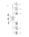
- FIG. 1 is a block diagram illustrating a configuration of a main part of a power supply system according to Embodiment 1.
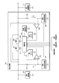
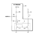
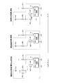
- FIG. It is a block diagram which shows the principal part structure of a prevention apparatus. It is a circuit diagram of the 1st constant current circuit. It is an equivalent circuit diagram of the 1st constant current circuit in each output state of a control part. It is a flowchart which shows the 1st prevention process which a control part performs. It is explanatory drawing which shows the effect of a prevention apparatus. It is explanatory drawing which shows the other effect of a prevention apparatus.
- FIG. 6 is a circuit diagram of a first constant current circuit in a second embodiment.
- FIG. 6 is a circuit diagram of a first constant current circuit in a third embodiment.
- FIG. 1 is a block diagram showing a main configuration of the power supply system according to the first embodiment.
- the power supply system 1 is suitably mounted on a vehicle and includes a prevention device 10, a first capacitor 11, a first load 12, a starter 13, a generator 14, a second load 15, and a second capacitor 16.
- One end of the prevention device 10 is connected to the positive electrode of the first capacitor 11 and one end of each of the first load 12 and the starter 13.
- the other end of the prevention device 10 is connected to one end of each of the generator 14 and the second load 15 and the positive electrode of the second battery 16.
- the negative electrodes of the first capacitor 11 and the second capacitor 16 and the other ends of the first load 12, the starter 13, the generator 14, and the second load 15 are grounded.
- the generator 14 generates AC regenerative power when, for example, the brake pedal of the vehicle is depressed and the vehicle speed is decelerated.
- the generator 14 rectifies the generated AC regenerative power into DC regenerative power.
- the generator 14 supplies the rectified DC regenerative power to the first capacitor 11 and the first load 12 via the prevention device 10 and also to the second load 15 and the second capacitor 16.
- the second load 15 is an electric device mounted on the vehicle, and is supplied with power from the first capacitor 11, the generator 14, and the second capacitor 16.
- the second battery 16 is an electric double layer capacitor, a lithium ion battery, or the like, and stores the electric power supplied from the generator 14.
- the second battery 16 is further fed with power from the first battery 11 via the prevention device 10 and stores the power supplied from the first battery 11.
- the second battery 16 supplies the stored power to the first battery 11 and the first load 12 via the prevention device 10 and also to the second load 15.
- the first battery 11 is, for example, a lead storage battery, and is supplied with power from the generator 14 and the second battery 16 via the prevention device 10, and stores the power supplied from the generator 14 and the second battery 16.
- the first capacitor 11 supplies the stored power to the first load 12 and the starter 13 and also supplies the second load 15 and the second capacitor 16 via the prevention device 10.
- the first load 12 is an electric device mounted on the vehicle, similar to the second load 15, and is supplied with power from the first capacitor 11, the generator 14, and the second capacitor 16.
- the starter 13 is a motor for starting an engine (not shown), and operates using the electric power stored in the first capacitor 11.
- the prevention device 10 has a prior signal that notifies in advance that the starter 13 is activated, a first activation signal that notifies in advance that the first load 12 is activated, and that the second load 15 is activated in advance. And a second operation signal to be notified.
- the prevention device 10 interrupts energization when a current equal to or greater than the cutoff threshold flows between both ends of the device, and prevents an overcurrent from flowing in the current path of the current flowing between both ends of the device.
- the prevention device 10 also cuts off the power supply when a prior signal is input. As a result, the starter 13 is fed by the first battery 11.
- the prevention apparatus 10 adjusts a cutoff threshold, when a 1st operation signal or a 2nd operation signal is input.
- FIG. 2 is a block diagram showing a main configuration of the prevention device 10.
- the prevention device 10 includes N-channel FETs 21 and 22, a control unit 23, a temperature detection unit 24, a first constant current circuit 25, a first comparator 26, a first timer 27, a second constant current circuit 28, and a second comparator 29.
- the diodes D1 and D2 are parasitic diodes of the FETs 21 and 22, respectively.
- the drain of the FET 21 and the cathode of the diode D1 are connected to one end of each of the generator 14 and the second load 15 and the positive electrode of the second capacitor 16.
- the anodes of the diodes D1 and D2 and the source of the FET 22 are connected to the source of the FET 21.
- the drain of the FET 22 is connected to the cathode of the diode D2, the positive electrode of the first capacitor 11, and one end of each of the first load 12 and the starter 13.
- the gates of the FETs 21 and 22 are connected to the control unit 23, and the control unit 23 is further connected to the temperature detection unit 24.
- the control unit 23 is also grounded.
- Each of the first load 12 and the second load 15 functions as a load in the claims.
- One end of the resistor R1 is connected to the drain of the FET 21, and the other end of the resistor R1 is connected to the first constant current circuit 25 and the negative terminal of the first comparator 26.
- the first constant current circuit 25 is further connected to the control unit 23 and is also grounded.
- the positive terminal of the first comparator 26 is connected to the drain of the FET 22, and the output terminal of the first comparator 26 is connected to the control unit 23.
- the first timer 27 is also connected to the control unit 23.
- One end of the resistor R2 is connected to the drain of the FET 22, and the other end of the resistor R2 is connected to the second constant current circuit 28 and the negative terminal of the second comparator 29.
- the second constant current circuit 28 is further connected to the control unit 23 and is also grounded.
- the positive terminal of the second comparator 29 is connected to the drain of the FET 21, and the output terminal of the second comparator 29 is connected to the control unit 23.
- FET21 and 22 each function as a switch. For each of the FETs 21 and 22, when a voltage higher than a certain voltage is applied to the gate by the control unit 23, a current can flow between the drain and the source, and each of the FETs 21 and 22 is turned on. Further, when the voltage applied to the gate by the control unit 23 is less than a certain voltage for each of the FETs 21 and 22, no current flows between the drain and the source, and the FETs 21 and 22 are turned off. The controller 23 simultaneously turns on / off the FETs 21 and 22 by adjusting the voltage applied to the gates of the FETs 21 and 22.
- the switch in the claims corresponds to the entire two FETs 21 and 22.
- the source of the FET 21 is connected to the source of the FET 22, the anode of the diode D1 is connected to the anode of the diode D2. Therefore, when each of the FETs 21 and 22 is off, no current flows through the diodes D1 and D2.
- the FETs 21 and 22 are provided in a current path of a current flowing between both ends of the prevention device 10.
- the first constant current circuit 25 allows a constant current to flow from the FET 21 side of the resistor R1 toward the other side.
- the value I1 of the current flowing through the first constant current circuit 25 is changed by the control unit 23.
- the control unit 23 functions as changing means in the claims.
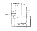
- FIG. 3 is a circuit diagram of the first constant current circuit 25.
- the first constant current circuit 25 includes a current mirror circuit 4 and resistors R3, R4, and R5.
- the current mirror circuit 4 has two NPN bipolar transistors 40 and 41. Each of the bipolar transistors 40 and 41 has a base, an emitter, and a collector. The other end of the resistor R1 is connected to the collector of the bipolar transistor 40 of the current mirror circuit 4.
- the base of the bipolar transistor 40 is connected to the base and collector of the bipolar transistor 41.
- the emitters of the bipolar transistors 40 and 41 are grounded, and the potentials at the emitters of the bipolar transistors 40 and 41 are substantially the same.
- the collector of the bipolar transistor 41 is connected to one end of the resistor R3, and the other end of the resistor R3 is connected to one end of each of the resistors R4 and R5.
- the other end of the resistor R4 is connected to the control unit 23, and a predetermined voltage Vcc is applied to the other end of the resistor R5.
- each of the bipolar transistors 40 and 41 a current having a large / small value flows between the emitter and the collector in accordance with the high / low voltage between the base and the emitter.
- the value of the current flowing between the collector and emitter of the bipolar transistor 40 is multiplied by a predetermined number between the collector and emitter of the bipolar transistor 40.
- the specified current flows.
- Each of the bipolar transistors 40 and 41 functions as the other and one transistor in the claims.
- the base, emitter and collector of each of the bipolar transistors 40 and 41 correspond to a first end, a second end and a third end in the claims.
- the voltage Vcc is applied between the other end of the resistor R5 and the emitter of the bipolar transistor 41.
- a current flows from the other end of the resistor R5 in the order of the resistor R3 and the collector and emitter of the bipolar transistor 41. Since the same voltage is applied to the bases of the bipolar transistors 40 and 41, a current having a value I1 obtained by multiplying the current value Iref flowing between the collector and emitter of the bipolar transistor 41 by a predetermined number flows through the resistor R1.
- the voltage Vcc is generated by a regulator (not shown), for example.
- the regulator generates a voltage Vcc from the output voltage of the second battery 16.
- the controller 23 changes the current value Iref by either adjusting the potential at the other end of the resistor R4 or opening the other end of the resistor R4. As a result, the current value I1 is changed. Specifically, the control unit 23 applies the voltage Vcc with reference to the potential of the emitter of the bipolar transistor 41 to the other end of the resistor R4, or grounds one end of the resistor R4 so that the other end of the resistor R4 is grounded. Adjust the potential at the edges.
- FIG. 4 is an equivalent circuit diagram of the first constant current circuit 25 in each output state of the control unit 23.
- the output state that the control unit 23 outputs to the other end of the resistor R4 includes a state where the voltage Vcc is applied to one end of the resistor R4, a state where one end of the resistor R4 is opened, and one end of the resistor R4 is grounded.
- resistors R3 and R5 are connected in series.
- the combined resistance value of the resistors R4 and R5 connected in parallel is smaller than the resistance value of the resistor R5. Therefore, the current value Iref when the control unit 23 opens the other end of the resistor R4 is smaller than the current value Iref when the control unit 23 applies the voltage Vcc to the other end of the resistor R4.
- the controller 23 adjusts the potential at the other end of the resistor R4 and opens the other end of the resistor R4, whereby the current value I1 that the first constant current circuit 25 passes through the resistor R1, That is, the value of the current flowing between the emitter and collector of the bipolar transistor 40 can be easily changed.
- the potential at the other end of the resistor R4 may be adjusted to a potential other than these in addition to the potential at the other end of the resistor R5 to which the voltage Vcc is applied and the ground potential. In this case, the current value Iref can be adjusted more finely.
- the first comparator 26 compares the potential at the drain of the FET 22 with the potential at the other end of the resistor R1.
- the first comparator 26 outputs a high level voltage from the output terminal to the control unit 23 when the potential at the drain of the FET 22 is higher than the potential at the other end of the resistor R1. Further, the first comparator 26 outputs a low level voltage from the output terminal to the control unit 23 when the potential at the drain of the FET 22 is lower than the potential at the other end of the resistor R1.
- the first comparator 26 functions as a comparison unit.
- the first timer 27 receives from the control unit 23 a start instruction for instructing the start of timekeeping and an end instruction for instructing the end of timekeeping.
- the first timer 27 starts timing when a start instruction is input from the control unit 23, and the first time measured by the first timer 27 is read by the control unit 23.
- the first timer 27 ends time counting when an end instruction is input from the control unit 23.
- the configuration and operation of the second constant current circuit 28, the second comparator 29, and the second timer 30 are the same as those of the first constant current circuit 25, the first comparator 26, and the first timer 27.
- the resistor R1 the FET 21, and the FET 22 described in the description of the first constant current circuit 25, the first comparator 26, and the first timer 27, respectively.
- the resistor R2 the FET 22 and the FET 21.
- the second constant current circuit 28 flows a constant current from the FET 22 side of the resistor R2 toward the other side, and the current value I2 that the second constant current circuit 28 flows is changed by the control unit 23.
- the second comparator 29 compares the potential at the drain of the FET 21 with the potential at the other end of the resistor R2.
- the controller 23 reads the second time measured by the second timer 30 from the second timer 30. Similar to the first comparator 26, the second comparator 29 functions as a comparison unit. And the control part 23 can change easily the value I2 of the electric current which the 2nd constant current circuit 28 flows into resistance R2.
- the temperature detection unit 24 is configured using, for example, a thermistor, and detects the temperature around the switch (hereinafter referred to as switch temperature). The switch temperature detected by the temperature detection unit 24 is read by the control unit 23.
- the controller 23 receives a pre-signal, a first operation signal, and a second operation signal. Further, a high level voltage or a low level voltage is input to the control unit 23 from the output terminals of the first comparator 26 and the second comparator 29.
- the control unit 23 turns off the FETs 21 and 22 when a prior signal is input. Then, the starter 13 is operated using the electric power of the first battery 11, and the engine is started. The controller 23 turns on the FETs 21 and 22 after a sufficient time has passed for the engine to start after turning off the FETs 21 and 22.
- the control unit 23 normally turns on the FETs 21 and 22 for other periods excluding the period related to the operation of the starter 13. While the FETs 21 and 22 are on, current flows between the drains of the FETs 21 and 22.
- the value of the current flowing between the drains of the FETs 21 and 22 is referred to as a switch current value.
- the control unit 23 turns off the FETs 21 and 22 when the switch current value is equal to or greater than a certain current value, and prevents an overcurrent from flowing between both ends of the prevention device 10.
- the controller 23 determines the value I1 of the current that the first constant current circuit 25 passes through the resistor R1 as described above. Change to Similarly, the control unit 23 changes the value I2 of the current that the second constant current circuit 28 passes through the resistor R2 based on the temperature detected by the temperature detection unit 24 and the second time measured by the second timer 30. To do. Furthermore, the control unit 23 switches the FETs 21 and 22 from on to off in accordance with the voltages output from the first comparator 26 and the second comparator 29.
- the FETs 21 and 22, the control unit 23, the temperature detection unit 24, the first constant current circuit 25, the first comparator 26, and the first timer 27 prevent an overcurrent from flowing from the drain of the FET 21 to the drain of the FET 22.
- the FETs 21 and 22, the control unit 23, the temperature detection unit 24, the second constant current circuit 28, the second comparator 29, and the second timer 30 prevent an overcurrent from flowing from the drain of the FET 22 to the drain of the FET 21.
- the control unit 23 performs a first prevention process to prevent an overcurrent from flowing from the drain of the FET 21 to the drain of the FET 22, and a second prevention process to prevent an overcurrent from flowing from the drain of the FET 22 to the drain of the FET 21. Execute the process.
- the control unit 23 executes the first prevention process and the second prevention process when the FETs 21 and 22 are turned on.
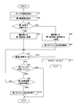
- FIG. 5 is a flowchart showing the first prevention process executed by the control unit 23.
- the control unit 23 reads the switch temperature detected by the temperature detection unit 24 from the temperature detection unit 24 (step S1), and sets the first current value to small / large according to the high / low of the read switch temperature. Set (step S2).
- the control part 23 determines whether the 1st load 12 will operate
- the control unit 23 determines that the first load 12 will be operated when the first operation signal is input, and the first load 12 is operating or stopped when the first operation signal is not input. It is determined that the first load 12 will not operate from now on.
- the control unit 23 also functions as a determination unit in the claims.
- the control unit 23 changes the current value I1 to the first current value set in step S2 (step S4).
- the controller 23 changes the current value I1 to a value obtained by adding a predetermined current value ⁇ I to the first current value set in step S2 (step S2).
- S5 The time measurement by the first timer 27 is started by outputting a start instruction to the first timer 27 (step S6).
- the control unit 23 increases the current value I1 from the first current value by the current value ⁇ I.
- the control unit 23 sets the first current value to small / large according to the switch temperature high / low, and sets the current value I1 to the first current value or the first current value.
- the current value is changed by adding ⁇ I. In other words, the control unit 23 changes the current value I1 to small / large according to the switch temperature high / low.
- Step S4 or Step S6 the control unit 23 determines whether or not the conduction between the drains of the FETs 21 and 22 should be cut off based on the voltage output from the first comparator 26 (Step S7). ).
- the potential at the drain of the FET 21 is Vb1
- the resistance value of the resistor R1 is r1
- the sum of the on-resistance values of the FETs 21 and 22 is rs
- the absolute value of the switch current value is Is.
- the value obtained by subtracting the potential at the other end of the resistor R1 from the potential at the drain of the FET 22 is (r1 ⁇ I1 ⁇ rs ⁇ Is).
- the first comparator 26 outputs a high level voltage from the output terminal to the control unit 23.
- the control unit 23 determines in step S7 that energization should not be interrupted.
- the first comparator 26 When the absolute value Is of the switch current value exceeds (r1 ⁇ I1 / rs), the first comparator 26 outputs a low level voltage to the control unit 23 from the output terminal. When the first comparator 26 outputs a low level voltage, the control unit 23 determines in step S7 that energization should be interrupted.
- the potential at the drain of the FET 22 is Vb2.
- the potential at the other end of the resistor R1 is (Vb2-rs ⁇ Is-r1 ⁇ I1).
- the value obtained by subtracting the potential at the other end of the resistor R1 from the potential Vb2 at the drain of the FET 22 is (rs ⁇ Is + r1 ⁇ I1), and always exceeds zero. Therefore, when current flows from the drain of the FET 22 to the drain of the FET 21, the first comparator 26 always outputs a high level voltage from the output terminal, and the control unit 23 should not cut off the energization in step S7. judge.
- the control unit 23 determines whether or not the first timer 27 is timing (step S8). When it is determined that the first timer 27 is measuring time (S8: YES), the control unit 23 determines whether the first time measured by the first timer 27 is equal to or longer than a preset set time. It is determined whether or not (step S9).
- the control unit 23 When it is determined that the first measured time is less than the set time (S9: NO), the control unit 23 returns the process to step S7, and the current value I1 is changed to the first time until the first measured time becomes equal to or greater than the set time. In a state where the current value is changed to the current value obtained by adding the current value ⁇ I to one current value, the determination as to whether or not to cut off energization is repeated.
- the control unit 23 When it is determined that the first measured time is equal to or longer than the set time (S9: YES), the control unit 23 outputs an end display to the first timer 27, thereby ending the time measurement by the first timer 27 (step S10). ). When it is determined that the first timer 27 has not timed (S8: NO), or after executing Step S10, the control unit 23 ends the first prevention process.
- the control unit 23 repeats the first prevention process while the FETs 21 and 22 are turned on.
- the first load 12 is in operation when the control unit 23 executes the first prevention process.
- the control unit 23 returns the current value I1 to the current value before the increase in step S5, that is, the first current value.
- control unit 23 determines that the energization should be interrupted (S7: YES), that is, the comparison result performed by the first comparator 26 indicates that the potential at the drain of the FET 22 is lower than the potential at the other end of the resistor R1. Is turned off, the FETs 21 and 22 are turned off (step S11). Thereafter, the control unit 23 ends the first prevention process.
- the second prevention process for preventing the overcurrent from flowing from the drain of the FET 22 to the drain of the FET 21 is the same as the first prevention process.
- the first load 12 the first constant current circuit 25, the first comparator 26, the first timer 27, the first current value, the current value I1, and the first operation signal in the description of the first prevention process.
- the first clock time correspond to the second load 15, the second constant current circuit 28, the second comparator 29, the second timer 30, the second current value, the current value I2, the second operation signal, and the second clock time, respectively. To do.
- the second current value is a current value set in a step corresponding to step S2 of the first prevention process in the second prevention process, and the switch temperature read from the temperature detection unit 24 is the same as the first current value. It is set to small / large according to the high / low of.
- the resistance value of the resistor R2 is r2.
- the potential at the drain of the FET 21 is (Vb2-rs ⁇ Is), and the other end of the resistor R2, that is, the second constant current circuit 28 side of the resistor R2
- the potential at one end is (Vb2-r2 ⁇ I2).
- the value obtained by subtracting the potential at the other end of the resistor R2 from the potential at the drain of the FET 22 is (r2 ⁇ I2 ⁇ rs ⁇ Is).
- the second comparator 29 outputs a high level voltage from the output terminal to the control unit 23.
- the control unit 23 It is determined that energization should not be interrupted.
- the second comparator 29 outputs a low level voltage from the output terminal, and in the second prevention process, the control unit 23 cuts off the energization. Determine that it should be.
- the potential at the other end of the resistor R2 is (Vb1 ⁇ rs ⁇ Is ⁇ r2 ⁇ I2). Since the potential at the drain of the FET 21 is Vb1, the value obtained by subtracting the potential at the other end of the resistor R2 from the potential at the drain of the FET 21 is (rs ⁇ Is + r2 ⁇ I2), which always exceeds zero. Therefore, when the current flows from the drain of the FET 21 to the drain of the FET 22, the second comparator 29 always outputs a high level voltage from the output terminal, and in the second prevention process, the control unit 23 should cut off the energization. It is determined that it is not.
- the control unit 23 repeats the first prevention process and the second prevention process until the FETs 21 and 22 are turned off in either the first prevention process or the second prevention process. At this time, the control unit 23 may be configured to alternately execute the first prevention process and the second prevention process, or may be configured to execute the first prevention process and the second prevention process in parallel. Also good.
- the first comparator 26 changes the threshold potential to be compared with the potential at the drain of the FET 22, that is, the potential at the other end of the resistor R1. Can do. Further, by changing the current value I2, the threshold potential that the second comparator 29 compares with the potential at the drain of the FET 21, that is, the potential at the other end of the resistor R2 can be changed.
- the on-resistance values of the FETs 21 and 22 vary.
- the manufacturing FETs 21 and 22 are turned off at an appropriate timing, and the energization is performed. Is cut off.
- FIG. 6 is an explanatory view showing the effect of the prevention device 10.
- a graph showing the relationship between the allowable current value, which is the absolute value of the allowable switch current value, and the switch temperature is drawn with a thin line.
- a graph showing the relationship between the cutoff threshold value, which is the absolute value of the switch current value at which the energization is cut off, and the switch temperature is drawn with a bold line.
- the allowable current value decreases as the switch temperature increases. This is because, when the switch temperature is high, even when the switch current value Is is relatively small, for example, the structures of the FETs 21 and 22 may change, and the FETs 21 and 22 may lose their functions as switches. Because there is.
- the first current value and the second current value are set to small / large according to the high / low of the switch temperature, so that the current values I1, I2 Each becomes smaller as the switch temperature is higher.
- the cutoff threshold value represented by (r1 ⁇ I1 / rs) in the first process and represented by (r2 ⁇ I2 / rs) in the second process is smaller as the switch temperature is higher. Therefore, as indicated by the thick line in FIG. 6, the cutoff threshold can be set to a value less than the allowable current value at each switch temperature. For this reason, failure of the FETs 21 and 22 can be surely prevented, and current can efficiently flow between the drains of the FETs 21 and 22.
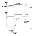
- FIG. 7 is an explanatory view showing another effect of the prevention device 10.
- FIG. 7 shows an example of the transition of the current value I1, the absolute value Is of the switch current value, and the cutoff threshold.
- the switch temperature is assumed to be constant.
- the control unit 23 changes the current value I1 to a value obtained by adding the current value ⁇ I to the first current value.
- the threshold potential to be compared with the potential at the drain of the FET 22, that is, the potential at the other end of the resistor R1 is lowered, and the cutoff threshold value expressed by (r1 ⁇ I1 / rs) is increased.
- the current value I1 is returned to the first current value after the design time has elapsed. .
- the cutoff threshold value also returns to the value when the current value I1 is the first current value.
- the set time is preferably longer than the time from when the first operation signal is input to the control unit 23 until the inrush current is generated and the absolute value Is of the switch current value is stabilized.
- the effect obtained by the control unit 23 executing the first prevention process is described with reference to FIG. 7, but the same effect can be obtained when the control unit 23 executes the second prevention process. That is, when the second load 15 is to be operated, the control unit 23 raises the current value I2 to a value obtained by adding the current value ⁇ I to the second current value. The probability of turning off each one is low. Further, when the set time has elapsed since the current value I2 was raised, the current value I2 is returned to the second current value. Therefore, the threshold potential to be compared with the potential at the drain of the FET 21 is set only during the period when the inrush current flows. It can be raised to increase the blocking threshold.
- FIG. 8 is a circuit diagram of the first constant current circuit 25 in the second embodiment.
- the second embodiment is different from the first embodiment in the circuit configurations of the first constant current circuit 25 and the second constant current circuit 28.
- the differences between the second embodiment and the first embodiment will be described. Since the other configuration except the configuration to be described later is the same as that of the first embodiment, the same reference numerals are given and the description thereof is omitted.
- the first constant current circuit 25 in the second embodiment includes a current mirror circuit 4 and resistors R3, R4, and R5, which are connected in the same manner as in the first embodiment.
- the first constant current circuit 25 according to the second embodiment further includes a resistor R6. One end of the resistor R6 is connected to one end of the resistor R5, and the other end of the resistor R6 is connected to the control unit 23.
- the control unit 23 performs the same operation on the other end of the resistor R6 as the operation performed on the other end of the resistor R4. That is, the control unit 23 adjusts the potential at the other end of the resistor R6 and opens the other end of the resistor R6.
- the current value Iref when the voltage Vcc is applied to the other end of the resistor R6 is the largest. Then, the current value Iref when the other end of the resistor R6 is opened is the next largest, and the current value Iref when the other end of the resistor R6 is grounded is the smallest.
- the addition of the resistor R6 allows the control unit 23 to control the current value Iref more finely.
- the number of values of the current value Iref is nine, and the control unit 23 can change the current value I1 to nine values.
- the potential at the other end of each of the resistors R4 and R6 may be adjusted to a potential other than these in addition to the potential at the other end of the resistor R5 to which the voltage Vcc is applied and the ground potential. In this case, the current value Iref can be adjusted more finely.
- the control unit 23 can control the current value I2 more finely.
- the control unit 23 in the second embodiment performs the first prevention process and the second prevention process similarly to the first embodiment, and only the configuration for changing the current values I1 and I2 is different from that in the first embodiment.
- the prevention device 10 in No. 2 has the same effect as that of the first embodiment.
- the number of resistors for adjusting the current value Iref is not limited to two, and may be three or more.
- the third and subsequent resistors are connected in the same manner as the resistor R4 or the resistor R6, and the controller 23 performs the same operation as that performed at the other end of the resistor R4.
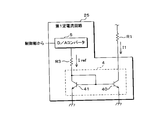
- FIG. 9 is a circuit diagram of the first constant current circuit 25 in the third embodiment.
- the third embodiment is different from the first embodiment in the circuit configurations of the first constant current circuit 25 and the second constant current circuit 28.
- the differences between the third embodiment and the first embodiment will be described. Since the other configuration except the configuration to be described later is the same as that of the first embodiment, the same reference numerals are given and the description thereof is omitted.
- the first constant current circuit 25 in the third embodiment has a current mirror circuit 4 and a resistor R3, which are connected in the same manner as in the first embodiment.
- the first constant current circuit 25 in the third embodiment further includes a D / A converter 5.
- the D / A converter 5 is connected to the other end of the resistor R3 and the control unit 23.
- One end of the resistor R3 is connected to the collector and base of the bipolar transistor 41.
- a digital signal indicating the height of the voltage to be applied between the other end of the resistor R 3 and the emitter of the bipolar transistor 41 is input to the D / A converter 5 from the control unit 23.
- the D / A converter 5 applies a voltage having a height indicated by the digital signal input from the control unit 23 between the other end of the resistor R 3 and the emitter of the bipolar transistor 41. Thereby, a current flows in the order of the other end of the resistor R3 and the collector and emitter of the bipolar transistor 41.
- the current value Iref (Vda ⁇ Vbe) / r3 (1)
- r3 is a resistance value of the resistor R3
- Vbe is a voltage between the base and the emitter of the bipolar transistor 41.
- the current value Iref becomes large / small according to the high / low of the voltage Vda.
- the control unit 23 adjusts the height of the voltage Vda by outputting a digital signal indicating various heights to the D / A converter 5. As a result, the control unit 23 changes the current value Iref and changes the current value I1. In the first constant current circuit 25 configured as described above, the control unit 25 can change the current value I1 with a simple configuration.
- the control unit 23 can change the current value I2 with a simple configuration. .
- the control unit 23 in the third embodiment performs the first prevention process and the second prevention process similarly to the first embodiment, and only the configuration for changing the current values I1 and I2 is different from the first embodiment.
- the prevention device 10 according to the third embodiment has the same effect as the first embodiment.
- the current value I1 increases from the first current value (or second current value) when the first load 12 (or second load 15) is to operate from now on. Then, the timing for returning to the first current value (or the second current value) is not limited after the set time has elapsed since the current value I1 (or the current value I2) is increased. For example, the absolute value Is of the switch current value is monitored, and when the absolute value Is of the switch current value is stabilized, the current value I1 (or current value I2) is changed to the first current value (or second current value). You may return.
- the current value I1 (or the current value I2) is changed, and the current value I1 (or the current value I2) is changed according to the switch temperature. Both of the processes to be changed need not be performed, and either one may be performed. Further, the condition for changing the current value I1 (or the current value I2) is not limited to the case where the first load 12 (or the second load 15) is to be operated or the switch temperature is changed. It may be a case where an instruction to change the current value I1 (or current value I2) is received from a person.
- the drain of the FET 21 is connected to the drain of the FET 22, the source of the FET 21 is connected to one end of the resistor R1 and the plus terminal of the second comparator 29, and the source of the FET 22 is connected to one end of the resistor R2. 1 may be connected to the plus terminal of the comparator 26.
- the cathodes of the diodes D1 and D2 are connected to the sources of the FETs 21 and 22, and the anodes are connected to the drains of the FETs 21 and 22, respectively. For this reason, since the cathode of the diode D1 is connected to the cathode of the diode D2, no current flows through the diodes D1 and D2 when the FETs 21 and 22 are off.
- each of the FETs 21 and 22 may be a P-channel FET or a bipolar transistor.
- One semiconductor switch may be used instead of the FETs 21 and 22.
- This semiconductor switch is preferably a switch in which no current flows between both ends of the semiconductor switch while it is off.
- the first constant current circuit 25 and the second constant current circuit 28 are not limited to the configuration using bipolar transistors, and may be configured using FETs. For example, when two N-channel FETs are used instead of the bipolar transistors 40 and 41, the gates, sources and drains of the two FETs correspond to the bases, emitters and collectors of the bipolar transistors 40 and 41, respectively. Furthermore, the configurations of the first constant current circuit 25 and the second constant current circuit 28 may be different.
Landscapes
- Emergency Protection Circuit Devices (AREA)
- Electronic Switches (AREA)
- Protection Of Static Devices (AREA)
Abstract
電流は、スイッチとして機能するFET21,22夫々のドレイン間を流れる。第1定電流回路25は抵抗R1のFET21側から他側に向けて一定の電流を流す。第1コンパレータ26は、FET22のドレインにおける電位が抵抗R1の第1定電流回路25側の一端における電位よりも高い場合にハイレベルの電圧を制御部23に出力する。更に、第1コンパレータ26は、FET22のドレインにおける電位が抵抗R1の第1定電流回路25側の一端における電位よりも低い場合にローレベルの電圧を制御部23に出力する。制御部23は、第1コンパレータ26がローレベルの電圧を出力した場合、FET21,22夫々をオフにする。更に、制御部23は第1定電流回路25が抵抗R1に流す電流を変更する。
Description
本発明は電流経路に過電流が流れることを防止する防止装置に関する。
車両には、電源から電気機器に給電する電源システムが搭載されている。この電源システムにおいて、短絡によって、電源及び電気機器を接続している導線に過電流が流れた場合、導線が発火する虞がある。このため、電源システムには、電源から電気機器への電流経路に過電流が流れることを防止する防止装置(例えば、特許文献1を参照)が搭載されている。
特許文献1に記載の防止装置では、FET(Field Effect Transistor)を介して電源から負荷に給電されている。そして、電源から負荷への電流経路に所定電流以上の電流が流れた場合にFETが電流経路に流れる電流を遮断する。
従来の防止装置として、電源から負荷への電流経路にスイッチが設けられており、スイッチの負荷側の一端における電位を閾値電位と比較する防止装置がある。例えば、スイッチが半導体スイッチである場合において、電流経路に大きい電流が流れたとき、スイッチのオン抵抗での電圧降下によって、スイッチの負荷側の一端における電位が大きく低下する。
前述した防止装置では、スイッチの負荷側の一端における電位が閾値電位よりも低くなった場合、スイッチをオフにする。これにより、電流経路に過電流が流れることが防止される。
しかしながら、負荷が誘導性である場合、負荷が作動した直後に電流経路に突入電流が流れる。前述した防止装置では、電流経路に突入電流が流れた場合に誤ってスイッチをオフにする虞がある。
また、電源システム内の温度は、車両が走行している環境又は負荷の作動状況等に応じて変化する。スイッチに流すことが許容される電流の値はスイッチ周辺の温度によって異なる。スイッチ周辺の温度が高い場合においては、スイッチに流れる電流の値が比較的に小さいときであってもスイッチが故障する可能性がある。従って、前述した防止装置において、閾値電位が一定の値に設定されている場合、スイッチに流すことが許容される電流の値を超える過電流が電流経路に流れる虞がある。
更に、前述した防止装置を大量に製造した場合において、スイッチのオン抵抗値のばらつきが大きい。このため、全ての防止装置について、閾値電位が同じである場合、スイッチのオン抵抗値が小さい防止装置では、スイッチの負荷側の一端における電位が閾値電位よりも高いときであっても電流経路に過電流が流れている虞がある。
本発明は斯かる事情に鑑みてなされたものであり、その目的とするところは、電流経路に過電流が流れることを確実に防止することができる防止装置を提供することにある。
本発明に係る防止装置は、電流経路に設けられたスイッチを備え、該スイッチをオフにすることによって前記電流経路に過電流が流れることを防止する防止装置において、一端が前記スイッチの一端に接続してある抵抗と、該抵抗の一端側から他端側に向けて一定の電流を流す定電流回路と、該定電流回路が流す電流の値を変更する変更手段と、前記スイッチ及び抵抗夫々の他端における電位を比較する比較部とを備え、該比較部が行った比較の結果が、前記スイッチの他端における電位が前記抵抗の他端における電位よりも低いことを示す場合に前記スイッチをオフにするように構成してあることを特徴とする。
本発明にあっては、例えば、スイッチの一端に電源が接続され、スイッチの他端に負荷が接続されており、電源から負荷への電流経路に電流が流れる。スイッチの一端に抵抗の一端が接続しており、定電流回路は、抵抗の一端側から他端側に向けて一定の電流を流す。そして、スイッチ及び抵抗夫々の他端における電位を比較する。
スイッチがオンである場合において、スイッチの他端における電位は電源の出力電圧からスイッチの両端間の電圧を引いた値であり、抵抗の他端における電位は、電源の出力電圧から、抵抗の両端間の電圧を引いた値である。定電流回路によって一定の電流が抵抗に流れているため、抵抗の両端間の電圧は一定である。そして、所定値以上の電流が電流経路に流れて、スイッチの両端間の電圧が所定電圧以上となった場合、スイッチの他端における電位が抵抗の他端における電位よりも低くなる。このとき、スイッチがオフにされるので、電流経路に過電流が流れることが防止される。
また、定電流回路が流す電流の値を変更する。これにより、抵抗の両端間の電圧を変更することが可能となるため、スイッチの他端における電位と比較する閾値電位を変更することができる。従って、例えば、スイッチの他端に誘導性負荷が接続されている場合、負荷が作動する直後から所定期間の間だけ、閾値電位を低い電位に変更することが可能である。また、スイッチ周辺の温度に応じて閾値電位を変更することも可能であり、装置ごとに閾値電位を変更することも可能である。閾値電位を適切に設定することによって、電流経路に過電流が流れることが確実に防止される。
本発明に係る防止装置は、前記スイッチ周辺の温度を検出する温度検出部を更に備え、前記変更手段は、前記温度検出部が検出した温度の高/低に応じて、前記定電流回路が流す電流の値を小/大に変更するように構成してあることを特徴とする。
本発明にあっては、スイッチ周辺の温度を検出する。そして、検出した温度が高い場合、即ち、スイッチが故障し易い場合においては、定電流回路が流す電流の値を小さい値に変更し、スイッチの他端における電位と比較する閾値電位を高くする。また、検出した温度が低い場合、即ち、スイッチが故障し難い場合においては、定電流回路が流す電流の値を大きい値に変更し、スイッチの他端における電位と比較する閾値電位を低くする。これにより、スイッチの故障が確実に防止され、かつ、電流経路に電流を効率的に流すことが可能となる。
本発明に係る防止装置は、前記スイッチの他端に負荷が接続してあり、該負荷が作動するか否かを判定する判定手段を備え、前記変更手段は、該判定手段によって前記負荷が作動すると判定された場合、前記定電流回路が流す電流の値を上昇させるように構成してあることを特徴とする。
本発明にあっては、スイッチの他端に負荷が接続してある。そして、負荷が作動すると判定した場合、定電流回路が流す電流の値を上昇させ、スイッチの他端における電位と比較する閾値電位を低くする。これにより、負荷が作動した直後に突入電流が発生した場合に、誤ってスイッチをオフにする確率は低い。
本発明に係る防止装置は、前記変更手段は、前記判定手段によって前記負荷が作動すると判定されてから所定時間が経過した場合に、前記定電流回路が流す電流の値を、上昇させる前の電流値に戻すように構成してあることを特徴とする。
本発明にあっては、負荷が作動すると判定して定電流回路が流す電流の値を上昇させた後、所定時間が経過した場合、定電流回路が流す電流の値を、上昇させる前の電流値に戻す。これにより、負荷が作動して電流経路に突入電流が流れる期間だけ、スイッチの他端における電位と比較する閾値電位を低くすることが可能となる。
本発明に係る防止装置は、前記定電流回路は、2つのトランジスタを備え、該2つのトランジスタ夫々は第1端、第2端及び第3端を有し、前記2つのトランジスタ夫々では、第1端及び第2端間の電圧に応じた値の電流が第2端及び第3端間に流れ、前記2つのトランジスタ中の一方のトランジスタにおける第1端及び第3端夫々が他方のトランジスタの第1端に接続されており、前記2つのトランジスタ夫々における第2端の電位は略同じであり、前記他方のトランジスタの第3端に前記抵抗の他端が接続されており、前記変更手段は、前記一方のトランジスタの第2端及び第3端間を流れる電流の値を変更することによって、前記定電流回路が流す電流の値を変更するように構成してあることを特徴とする。
本発明にあっては、定電流回路は2つのトランジスタを備え、2つのトランジスタ夫々は第1端、第2端及び第3端を有する。2つのトランジスタ夫々では、第1端及び第2端間の電圧に応じた値の電流が第2端及び第3端間に流れる。2つのトランジスタ中の一方のトランジスタにおける第1端及び第3端は他方のトランジスタの第1端に接続されており、2つのトランジスタ夫々における第2端の電位は略同じである。そして、他方のトランジスタの第3端に抵抗の他端が接続されている。
以上のように2つのトランジスタが接続されている場合、2つのトランジスタ夫々における第1端及び第2端間の電圧は略一致する。このため、2つのトランジスタについて、第1端及び第2端間の電圧に対して、第2端及び第3端間を流れる電流の値が同様に変化する場合、一方のトランジスタの第2端及び第3端間に流れる電流の値を所定数倍にした値の電流が他方のトランジスタの第2端及び第3端間に流れる。そして、一方のトランジスタの第2端及び第3端間に流れる電流の値を変更することによって、定電流回路が流す電流、即ち、他方のトランジスタにおける第2端及び第3端間を流れる電流の値が容易に変更される。
2つのトランジスタ夫々がNPN型のバイポーラトランジスタである場合、第1端はベースであり、第2端はエミッタであり、第3端はコレクタである。
2つのトランジスタ夫々がNPN型のバイポーラトランジスタである場合、第1端はベースであり、第2端はエミッタであり、第3端はコレクタである。
本発明によれば、電流経路に過電流が流れることを確実に防止することができる。
以下、本発明をその実施の形態を示す図面に基づいて詳述する。
(実施の形態1)
図1は実施の形態1における電源システムの要部構成を示すブロック図である。この電源システム1は、車両に好適に搭載され、防止装置10、第1蓄電器11、第1負荷12、スタータ13、発電機14、第2負荷15及び第2蓄電器16を備える。防止装置10の一端は、第1蓄電器11の正極と、第1負荷12及びスタータ13夫々の一端とに接続されている。防止装置10の他端は、発電機14及び第2負荷15夫々の一端と、第2蓄電器16の正極とに接続されている。第1蓄電器11及び第2蓄電器16夫々の負極と、第1負荷12、スタータ13、発電機14及び第2負荷15夫々の他端とは接地されている。
(実施の形態1)
図1は実施の形態1における電源システムの要部構成を示すブロック図である。この電源システム1は、車両に好適に搭載され、防止装置10、第1蓄電器11、第1負荷12、スタータ13、発電機14、第2負荷15及び第2蓄電器16を備える。防止装置10の一端は、第1蓄電器11の正極と、第1負荷12及びスタータ13夫々の一端とに接続されている。防止装置10の他端は、発電機14及び第2負荷15夫々の一端と、第2蓄電器16の正極とに接続されている。第1蓄電器11及び第2蓄電器16夫々の負極と、第1負荷12、スタータ13、発電機14及び第2負荷15夫々の他端とは接地されている。
発電機14は、例えば、車両のブレーキペダルが踏み込まれており、かつ、車速が減速している場合に交流の回生電力を発生する。発電機14は、発生した交流の回生電力を直流の回生電力に整流する。発電機14は、整流した直流の回生電力を、防止装置10を介して第1蓄電器11及び第1負荷12に供給すると共に、第2負荷15及び第2蓄電器16にも供給する。
第2負荷15は、車両に搭載される電気機器であり、第1蓄電器11、発電機14及び第2蓄電器16から給電される。
第2蓄電器16は、電気二重層キャパシタ又はリチウムイオン電池等であり、発電機14から供給された電力を蓄える。第2蓄電器16は、更に、防止装置10を介して、第1蓄電器11から給電され、第1蓄電器11から供給された電力を蓄える。第2蓄電器16は、蓄えた電力を、防止装置10を介して第1蓄電器11及び第1負荷12に供給すると共に、第2負荷15に供給する。
第2蓄電器16は、電気二重層キャパシタ又はリチウムイオン電池等であり、発電機14から供給された電力を蓄える。第2蓄電器16は、更に、防止装置10を介して、第1蓄電器11から給電され、第1蓄電器11から供給された電力を蓄える。第2蓄電器16は、蓄えた電力を、防止装置10を介して第1蓄電器11及び第1負荷12に供給すると共に、第2負荷15に供給する。
第1蓄電器11は、例えば鉛蓄電池であり、発電機14及び第2蓄電器16夫々から防止装置10を介して給電され、発電機14及び第2蓄電器16から供給された電力を蓄える。第1蓄電器11は、蓄えた電力を、第1負荷12及びスタータ13に供給すると共に、防止装置10を介して第2負荷15及び第2蓄電器16に供給する。
第1負荷12は、第2負荷15と同様に車両に搭載される電気機器であり、第1蓄電器11、発電機14及び第2蓄電器16から給電される。
スタータ13は、図示しないエンジンを始動させるためのモータであり、第1蓄電器11が蓄えた電力を用いて作動する。
スタータ13は、図示しないエンジンを始動させるためのモータであり、第1蓄電器11が蓄えた電力を用いて作動する。
防止装置10には、スタータ13が作動することを事前に通知する事前信号と、第1負荷12が作動することを事前に通知する第1作動信号と、第2負荷15が作動することを事前に通知する第2作動信号とが入力される。
防止装置10は、自身の両端間に遮断閾値以上の電流が流れた場合に、通電を遮断し、自身の両端間を流れる電流の電流経路に過電流が流れることを防止する。防止装置10は、事前信号が入力された場合にも通電を遮断する。これにより、スタータ13は第1蓄電器11によって給電される。また、防止装置10は、第1作動信号又は第2作動信号が入力された場合に遮断閾値を調整する。
図2は防止装置10の要部構成を示すブロック図である。防止装置10は、Nチャネル型のFET21,22、制御部23、温度検出部24、第1定電流回路25、第1コンパレータ26、第1タイマ27、第2定電流回路28、第2コンパレータ29、第2タイマ30、ダイオードD1,D2及び抵抗R1,R2を有する。ダイオードD1,D2夫々はFET21,22の寄生ダイオードである。
発電機14及び第2負荷15夫々の一端と第2蓄電器16の正極とには、FET21のドレインと、ダイオードD1のカソードとが接続されている。FET21のソースには、ダイオードD1,D2夫々のアノードと、FET22のソースとが接続されている。FET22のドレインには、ダイオードD2のカソードと、第1蓄電器11の正極と、第1負荷12及びスタータ13夫々の一端とが接続されている。FET21,22夫々のゲートは制御部23に接続されており、制御部23には更に温度検出部24に接続されている。制御部23は接地もされている。
第1負荷12及び第2負荷15夫々は請求の範囲における負荷として機能する。
第1負荷12及び第2負荷15夫々は請求の範囲における負荷として機能する。
FET21のドレインに抵抗R1の一端が接続してあり、抵抗R1の他端には、第1定電流回路25と、第1コンパレータ26のマイナス端子とが接続されている。第1定電流回路25は、更に制御部23に接続されており、接地もされている。第1コンパレータ26のプラス端子は、FET22のドレインに接続されており、第1コンパレータ26の出力端子は制御部23に接続されている。第1タイマ27も制御部23に接続されている。
FET22のドレインに抵抗R2の一端が接続してあり、抵抗R2の他端には、第2定電流回路28と、第2コンパレータ29のマイナス端子とが接続されている。第2定電流回路28は、更に制御部23に接続されており、接地もされている。第2コンパレータ29のプラス端子はFET21のドレインに接続されており、第2コンパレータ29の出力端子は制御部23に接続されている。
FET21,22夫々はスイッチとして機能する。FET21,22夫々について、制御部23によってゲートに一定電圧以上の電圧が印加された場合、ドレイン及びソース間に電流を流すことが可能となり、FET21,22夫々はオンとなる。また、FET21,22夫々について、制御部23によってゲートに印加されている電圧が一定電圧未満である場合、ドレイン及びソース間に電流が流れず、FET21,22夫々はオフとなる。制御部23は、FET21,22夫々のゲートに印加されている電圧の高さを調整することによって、FET21,22夫々を同時的にオン/オフする。請求の範囲におけるスイッチは、2つのFET21,22全体に相当する。
FET21のソースがFET22のソースに接続されているため、ダイオードD1のアノードがダイオードD2のアノードに接続される。従って、FET21,22夫々がオフである場合に、ダイオードD1,D2を介して電流が流れることはない。
FET21,22は防止装置10の両端間に流れる電流の電流経路に設けられている。
FET21,22は防止装置10の両端間に流れる電流の電流経路に設けられている。
第1定電流回路25は、抵抗R1のFET21側から他側に向けて一定の電流を流す。第1定電流回路25が流す電流の値I1は制御部23によって変更される。制御部23は請求の範囲における変更手段として機能する。
図3は第1定電流回路25の回路図である。第1定電流回路25は、カレントミラー回路4及び抵抗R3,R4,R5を有する。カレントミラー回路4は2つのNPN型のバイポーラトランジスタ40,41を有する。バイポーラトランジスタ40,41夫々はベース、エミッタ及びコレクタを有する。抵抗R1の他端は、カレントミラー回路4のバイポーラトランジスタ40のコレクタに接続されている。バイポーラトランジスタ40のベースは、バイポーラトランジスタ41のベース及びコレクタに接続されている。バイポーラトランジスタ40,41夫々のエミッタは接地されており、バイポーラトランジスタ40,41夫々のエミッタにおける電位は略同じである。バイポーラトランジスタ41のコレクタは抵抗R3の一端に接続されており、抵抗R3の他端は抵抗R4,R5夫々の一端に接続されている。抵抗R4の他端は制御部23に接続されており、抵抗R5の他端は所定の電圧Vccが印加されている。
バイポーラトランジスタ40,41夫々では、ベース及びエミッタ間の電圧の高/低に応じて、値が大/小となる電流がエミッタ及びコレクタ間に流れる。バイポーラトランジスタ40,41夫々のベース及びエミッタ間に同一の電圧が印加された場合、バイポーラトランジスタ40のコレクタ及びエミッタ間には、バイポーラトランジスタ41のコレクタ及びエミッタ間に流れる電流の値を所定数倍にした値の電流が流れる。
バイポーラトランジスタ40,41夫々は、請求の範囲における他方及び一方のトランジスタとして機能する。バイポーラトランジスタ40,41夫々のベース、エミッタ及びコレクタは請求の範囲における第1端、第2端及び第3端に相当する。
バイポーラトランジスタ40,41夫々は、請求の範囲における他方及び一方のトランジスタとして機能する。バイポーラトランジスタ40,41夫々のベース、エミッタ及びコレクタは請求の範囲における第1端、第2端及び第3端に相当する。
第1定電流回路25では、電圧Vccが抵抗R5の他端とバイポーラトランジスタ41のエミッタとの間に印加されている。これにより、電流が抵抗R5の他端から抵抗R3並びにバイポーラトランジスタ41のコレクタ及びエミッタの順に流れる。そして、バイポーラトランジスタ40,41夫々のベースに同一の電圧が印加されるので、バイポーラトランジスタ41のコレクタ及びエミッタ間を流れる電流の値Irefを所定数倍した値I1の電流が抵抗R1に流れる。
なお、電圧Vccは例えば図示しないレギュレータによって生成される。レギュレータは例えば第2蓄電器16の出力電圧から電圧Vccを生成する。
なお、電圧Vccは例えば図示しないレギュレータによって生成される。レギュレータは例えば第2蓄電器16の出力電圧から電圧Vccを生成する。
制御部23は、抵抗R4の他端における電位の調整、及び、抵抗R4の他端の開放のいずれかを行うことによって、電流値Irefを変更する。これにより、電流値I1を変更する。
具体的には、制御部23は、抵抗R4の他端にバイポーラトランジスタ41のエミッタの電位を基準とした電圧Vccを印加するか、又は、抵抗R4の一端を接地することによって、抵抗R4の他端における電位を調整する。
具体的には、制御部23は、抵抗R4の他端にバイポーラトランジスタ41のエミッタの電位を基準とした電圧Vccを印加するか、又は、抵抗R4の一端を接地することによって、抵抗R4の他端における電位を調整する。
図4は制御部23の各出力状態における第1定電流回路25の等価回路図である。制御部23が抵抗R4の他端へ出力する出力状態は、抵抗R4の一端に電圧Vccが印加されている状態、抵抗R4の一端が開放されている状態、及び、抵抗R4の一端が接地されている状態のいずれかである。
図4の左側、中央及び右側夫々には、抵抗R4の他端に電圧Vccが印加されている場合、抵抗R4の他端が開放されている場合、及び、抵抗R4の一端が接地されている場合夫々における第1定電流回路25の等価回路が示されている。第1定電流回路25の等価回路は破線で囲まれている。
制御部23が抵抗R4の他端に電圧Vccを印加した場合、図4の左側に示す等価回路からわかるように、抵抗R4,R5が並列に接続される。従って、抵抗R3と、並列に接続された抵抗R4,R5の合成抵抗とが直列に接続されている。
次に、制御部23が抵抗R4の他端を開放した場合、抵抗R4に電流が流れることはない。このため、図4の中央に示す等価回路からわかるように、抵抗R3,R5が直列に接続されている。ここで、並列に接続された抵抗R4,R5の合成抵抗値は抵抗R5の抵抗値よりも小さい。このため、制御部23が抵抗R4の他端を開放した場合における電流値Irefは、制御部23が抵抗R4の他端に電圧Vccを印加した場合における電流値Irefよりも小さい。
次に、制御部23が抵抗R4の他端を接地した場合、図4の右側に示す等価回路からわかるように、抵抗R5を流れた電流の一部が、抵抗R3に流れず、抵抗R4に流れる。このため、制御部23が抵抗R4の他端を接地した場合における電流値Irefは、制御部23が抵抗R4の他端を開放した場合における電流値Irefよりも小さい。
以上のように、制御部23は抵抗R4の他端における電位の調整及び抵抗R4の他端の開放のいずれかを行うことによって、第1定電流回路25が抵抗R1に流す電流の値I1、即ち、バイポーラトランジスタ40のエミッタ及びコレクタ間に流れる電流の値を容易に変更することができる。
なお、抵抗R4の他端における電位を、電圧Vccが印加されている抵抗R5の他端における電位と接地電位とに加えて、これら以外の電位に調整してもよい。この場合、電流値Irefをより細かく調整することが可能である。
なお、抵抗R4の他端における電位を、電圧Vccが印加されている抵抗R5の他端における電位と接地電位とに加えて、これら以外の電位に調整してもよい。この場合、電流値Irefをより細かく調整することが可能である。
第1コンパレータ26は、図2に示すように、FET22のドレインにおける電位と、抵抗R1の他端における電位とを比較する。第1コンパレータ26は、FET22のドレインにおける電位が、抵抗R1の他端における電位よりも高い場合、出力端子からハイレベルの電圧を制御部23に出力する。更に、第1コンパレータ26は、FET22のドレインにおける電位が、抵抗R1の他端における電位よりも低い場合、出力端子からローレベルの電圧を制御部23に出力する。第1コンパレータ26は比較部として機能する。
第1タイマ27には、計時の開始を指示する開始指示と、計時の終了を指示する終了指示とが制御部23から入力される。第1タイマ27は、制御部23から開始指示が入力された場合に計時を開始し、第1タイマ27が計時した第1計時時間が制御部23によって読込まれる。第1タイマ27は、制御部23から終了指示が入力された場合に計時を終了する。
第2定電流回路28、第2コンパレータ29及び第2タイマ30夫々の構成及び作用は、第1定電流回路25、第1コンパレータ26及び第1タイマ27と同様である。第2定電流回路28、第2コンパレータ29及び第2タイマ30の構成及び作用について、第1定電流回路25、第1コンパレータ26及び第1タイマ27の説明で述べた抵抗R1、FET21及びFET22夫々は、抵抗R2、FET22及びFET21に対応する。
従って、第2定電流回路28は、抵抗R2のFET22側から他側に向けて一定の電流を流し、第2定電流回路28が流す電流の値I2は制御部23によって変更される。更に、第2コンパレータ29は、FET21のドレインにおける電位と、抵抗R2の他端における電位とを比較する。制御部23は第2タイマ30が計時した第2計時時間を第2タイマ30から読込む。第2コンパレータ29は第1コンパレータ26と同様に比較部として機能する。そして、制御部23は、第2定電流回路28が抵抗R2に流す電流の値I2を容易に変更することができる。
温度検出部24は、例えば、サーミスタを用いて構成され、スイッチ周辺の温度(以下ではスイッチ温度と記載する)を検出する。温度検出部24が検出したスイッチ温度は制御部23によって読込まれる。
制御部23には、事前信号、第1作動信号及び第2作動信号が入力される。更に、制御部23には、第1コンパレータ26及び第2コンパレータ29夫々の出力端子からハイレベルの電圧、又は、ローレベルの電圧が入力される。
制御部23は、事前信号が入力された場合、FET21,22をオフにする。そして、スタータ13が第1蓄電器11の電力を用いて作動し、エンジンが始動する。制御部23は、FET21,22をオフにしてから、エンジンが始動するために十分な時間が経過した後、FET21,22をオンにする。
制御部23は、スタータ13の作動に関する期間を除く、他の期間については、通常、FET21,22をオンにしている。FET21,22がオンである期間、FET21,22夫々のドレイン間に電流が流れる。以下では、FET21,22夫々のドレイン間に流れる電流の値をスイッチ電流値と記載する。
制御部23は、スイッチ電流値が一定の電流値以上である場合にFET21,22をオフにし、防止装置10の両端間に過電流が流れることを防止する。
制御部23は、スイッチ電流値が一定の電流値以上である場合にFET21,22をオフにし、防止装置10の両端間に過電流が流れることを防止する。
制御部23は、温度検出部24が検出した温度と、第1タイマ27が計時した第1計時時間とに基づいて第1定電流回路25が抵抗R1に流す電流の値I1を、前述したように変更する。同様に、制御部23は、温度検出部24が検出した温度と、第2タイマ30が計時した第2計時時間とに基づいて第2定電流回路28が抵抗R2に流す電流の値I2を変更する。更に、制御部23は、第1コンパレータ26及び第2コンパレータ29が出力した電圧に応じてFET21,22夫々をオンからオフに切替える。
FET21,22、制御部23、温度検出部24、第1定電流回路25、第1コンパレータ26及び第1タイマ27によって、FET21のドレインからFET22のドレインに過電流が流れることを防止する。そして、FET21,22、制御部23、温度検出部24、第2定電流回路28、第2コンパレータ29及び第2タイマ30によって、FET22のドレインからFET21のドレインに過電流が流れることを防止する。制御部23は、FET21のドレインからFET22のドレインに過電流が流れる防止するために第1防止処理を実行し、FET22のドレインからFET21のドレインに過電流が流れることを防止するために第2防止処理を実行する。制御部23は、FET21,22夫々をオンしている場合に第1防止処理及び第2防止処理を実行する。
図5は制御部23が実行する第1防止処理を示すフローチャートである。制御部23は、まず、温度検出部24が検出したスイッチ温度を、温度検出部24から読込み(ステップS1)、読込んだスイッチ温度の高/低に応じて第1電流値を小/大に設定する(ステップS2)。次に、制御部23は、第1作動信号が入力されたか否かに基づいて、第1負荷12がこれから作動するか否かを判定する(ステップS3)。ここで、制御部23は、第1作動信号が入力されている場合に第1負荷12がこれから作動すると判定し、第1作動信号が入力されていない場合、第1負荷12が作動中又は停止中であるとして、第1負荷12がこれから作動しないと判定する。制御部23は請求の範囲における判定手段としても機能する。
制御部23は、第1負荷12が作動しないと判定した場合(S3:NO)、電流値I1を、ステップS2で設定した第1電流値に変更する(ステップS4)。制御部23は、第1負荷12が作動すると判定した場合(S3:YES)、電流値I1を、ステップS2で設定した第1電流値に所定の電流値ΔIを加算した値に変更し(ステップS5)、第1タイマ27に開始指示を出力することによって第1タイマ27による計時を開始する(ステップS6)。
以上のように、制御部23は、ステップS3で第1負荷12が作動すると判定した場合、電流値I1を第1電流値から電流値ΔIだけ上昇させる。
また、制御部23は、ステップS2でスイッチ温度の高/低に応じて第1電流値を小/大に設定し、電流値I1を、第1電流値、又は、第1電流値に電流値ΔIを加算した電流値に変更する。言い換えると、制御部23は、スイッチ温度の高/低に応じて電流値I1を小/大に変更する。
また、制御部23は、ステップS2でスイッチ温度の高/低に応じて第1電流値を小/大に設定し、電流値I1を、第1電流値、又は、第1電流値に電流値ΔIを加算した電流値に変更する。言い換えると、制御部23は、スイッチ温度の高/低に応じて電流値I1を小/大に変更する。
制御部23は、ステップS4又はステップS6を実行した後、第1コンパレータ26が出力している電圧に基づいて、FET21,22夫々のドレイン間の通電を遮断すべきか否かを判定する(ステップS7)。
FET21のドレインにおける電位をVb1とし、抵抗R1の抵抗値をr1とし、FET21,22夫々のオン抵抗値の和をrsとし、スイッチ電流値の絶対値をIsとする。
電流がFET21のドレインからFET22のドレインへ流れている場合、FET22のドレインにおける電位は、(Vb1-rs×Is)であり、抵抗R1の他端、即ち、抵抗R1の第1定電流回路25側の一端における電位は(Vb1-r1×I1)である。
電流がFET21のドレインからFET22のドレインへ流れている場合、FET22のドレインにおける電位は、(Vb1-rs×Is)であり、抵抗R1の他端、即ち、抵抗R1の第1定電流回路25側の一端における電位は(Vb1-r1×I1)である。
FET22のドレインにおける電位から抵抗R1の他端における電位を引いた値は、(r1×I1-rs×Is)である。スイッチ電流値の絶対値Isが(r1×I1/rs)以下である場合、第1コンパレータ26は出力端子からハイレベルの電圧を制御部23に出力する。制御部23は、第1コンパレータ26がハイレベルの電圧を出力している場合、ステップS7では、通電を遮断すべきではないと判定する。
スイッチ電流値の絶対値Isが(r1×I1/rs)を超えた場合、第1コンパレータ26は出力端子からローレベルの電圧を制御部23に出力する。制御部23は、第1コンパレータ26がローレベルの電圧を出力している場合、ステップS7では、通電を遮断すべきであると判定する。
FET22のドレインにおける電位をVb2とする。電流がFET22のドレインからFET21のドレインへ流れている場合、抵抗R1の他端における電位は(Vb2-rs×Is-r1×I1)である。FET22のドレインにおける電位Vb2から抵抗R1の他端における電位を引いた値は、(rs×Is+r1×I1)であり、常にゼロを超えている。
このため、電流がFET22のドレインからFET21のドレインへ流れている場合、第1コンパレータ26は常に出力端子からハイレベルの電圧を出力し、制御部23はステップS7で通電を遮断すべきではないと判定する。
このため、電流がFET22のドレインからFET21のドレインへ流れている場合、第1コンパレータ26は常に出力端子からハイレベルの電圧を出力し、制御部23はステップS7で通電を遮断すべきではないと判定する。
制御部23は、通電を遮断すべきではないと判定した場合(S7:NO)、第1タイマ27が計時しているか否かを判定する(ステップS8)。制御部23は、第1タイマ27が計時していると判定した場合(S8:YES)、第1タイマ27が計時している第1計時時間が、予め設定されている設定時間以上であるか否かを判定する(ステップS9)。
制御部23は、第1計時時間が設定時間未満であると判定した場合(S9:NO)、処理をステップS7に戻し、第1計時時間が設定時間以上となるまで、電流値I1が、第1電流値に電流値ΔIを加えた電流値に変更してある状態で、通電を遮断すべきか否かの判定を繰り返す。
制御部23は、第1計時時間が設定時間以上であると判定した場合(S9:YES)、終了表示を第1タイマ27に出力することによって、第1タイマ27による計時を終了する(ステップS10)。制御部23は、第1タイマ27が計時をしていないと判定した場合(S8:NO)、又はステップS10を実行した後、第1防止処理を終了する。
制御部23は、FET21,22をオンにしている間、第1防止処理を繰り返す。ステップS3で第1負荷12が作動すると判定されてから設定時間が経過して、次に、制御部23が第1防止処理を実行したとき、第1負荷12は作動中であるため、スイッチ温度に変化がない限り、制御部23は、電流値I1を、ステップS5で上昇させる前の電流値、即ち、第1電流値に戻す。
制御部23は、通電を遮断すべきと判定した場合(S7:YES)、即ち、第1コンパレータ26が行った比較結果が、FET22のドレインにおける電位が抵抗R1の他端における電位よりも低いことを示す場合、FET21,22をオフにする(ステップS11)。その後、制御部23は第1防止処理を終了する。
FET22のドレインからFET21のドレインへ過電流が流れることを防止する第2防止処理は、第1防止処理と同様である。第2防止処理の説明では、第1防止処理の説明における第1負荷12、第1定電流回路25、第1コンパレータ26、第1タイマ27、第1電流値、電流値I1、第1作動信号及び第1計時時間夫々は、第2負荷15、第2定電流回路28、第2コンパレータ29、第2タイマ30、第2電流値、電流値I2、第2作動信号及び第2計時時間に対応する。第2電流値は、第2防止処理において、第1防止処理のステップS2に対応するステップで設定される電流値であり、第1電流値と同様に、温度検出部24から読込んだスイッチ温度の高/低に応じて小/大に設定される。
抵抗R2の抵抗値をr2とする。電流がFET22のドレインからFET21のドレインへ流れている場合、FET21のドレインにおける電位は、(Vb2-rs×Is)であり、抵抗R2の他端、即ち、抵抗R2の第2定電流回路28側の一端における電位は(Vb2-r2×I2)である。
FET22のドレインにおける電位から抵抗R2の他端における電位を引いた値は、(r2×I2-rs×Is)である。スイッチ電流値の絶対値Isが(r2×I2/rs)以下である場合、第2コンパレータ29は出力端子からハイレベルの電圧を制御部23に出力し、第2防止処理では、制御部23は通電を遮断すべきではないと判定する。そして、スイッチ電流の絶対値Isが(r2×I2/rs)を超えた場合、第2コンパレータ29は出力端子からローレベルの電圧を出力し、第2防止処理において、制御部23は通電を遮断すべきであると判定する。
電流がFET21のドレインからFET22のドレインへ流れている場合、抵抗R2の他端における電位は(Vb1-rs×Is-r2×I2)である。FET21のドレインにおける電位はVb1であるため、FET21のドレインにおける電位から抵抗R2の他端における電位を引いた値は、(rs×Is+r2×I2)であり、常にゼロを超えている。
このため、電流がFET21のドレインからFET22のドレインへ流れている場合、第2コンパレータ29は常に出力端子からハイレベルの電圧を出力し、第2防止処理では、制御部23は通電を遮断すべきではないと判定する。
このため、電流がFET21のドレインからFET22のドレインへ流れている場合、第2コンパレータ29は常に出力端子からハイレベルの電圧を出力し、第2防止処理では、制御部23は通電を遮断すべきではないと判定する。
制御部23は、第1防止処理及び第2防止処理のいずれかでFET21,22夫々をオフにするまで、第1防止処理及び第2防止処理を繰り返す。このとき、制御部23は、第1防止処理及び第2防止処理を交互に実行するように構成されてもよいし、第1防止処理及び第2防止処理を並行に実行するように構成されてもよい。
以上のように構成された防止装置10では、電流値I1を変更することによって、第1コンパレータ26がFET22のドレインにおける電位と比較する閾値電位、即ち、抵抗R1の他端における電位を変更することができる。また、電流値I2を変更することによって、第2コンパレータ29がFET21のドレインにおける電位と比較する閾値電位、即ち、抵抗R2の他端における電位を変更することができる。以上に述べた2つの閾値電位夫々を適切に設定することによって、電流経路に過電流が流れることを確実に防止することができる。
また、防止装置10を大量に製造した場合に、FET21,22のオン抵抗値がばらつく。しかしながら、防止装置10では、電流値I1,I2、具体的には第1電流値及び第2電流値を微調整することによって、製造されたFET21,22夫々は適切なタイミングでオフにされ、通電が遮断される。
図6は防止装置10の効果を示す説明図である。図6には、許容されるスイッチ電流値の絶対値である許容電流値とスイッチ温度との関係を示すグラフが細線で描かれている。更に、図6には、通電が遮断されるスイッチ電流値の絶対値である遮断閾値と、スイッチ温度との関係を示すグラフが太線で描かれている。
図6の細線で示されているように許容電流値はスイッチ温度の上昇と共に低下する。これは、スイッチ温度が高い場合、スイッチ電流値Isが比較的に小さいときであっても、例えばFET21,22夫々の構造が変化してしまい、FET21,22夫々がスイッチとしての機能を失う可能性があるためである。
第1防止処理及び第2防止処理では、前述したように第1電流値及び第2電流値夫々は、スイッチ温度の高/低に応じて小/大に設定されるので、電流値I1,I2夫々は、スイッチ温度が高い程小さくなる。これにより、第1処理では(r1×I1/rs)によって表され、第2処理では(r2×I2/rs)によって表される遮断閾値は、スイッチ温度が高い程小さい。従って、図6の太線で示すように、各スイッチ温度において、遮断閾値を許容電流値未満の値に設定することが可能となる。このため、FET21,22の故障を確実に防止することができ、FET21,22のドレイン間に電流を効率的に流すことができる。
図7は防止装置10の他の効果を示す説明図である。図7には、電流値I1、スイッチ電流値の絶対値Is及び遮断閾値の推移の一例が示されている。ここではスイッチ温度は一定であるとする。前述したように、第1防止処理において、第1作動信号が制御部23に入力された場合、制御部23は電流値I1を第1電流値に電流値ΔIを加算した値に変更する。これにより、FET22のドレインにおける電位と比較する閾値電位、即ち、抵抗R1の他端における電位が低くなり、(r1×I1/rs)で表される遮断閾値が上昇する。従って、第1負荷12が停止状態から作動することによって、FET21,22を介して突入電流が流れ、スイッチ電流値の絶対値Isが一時的に高い値となった場合に、誤ってFET21,22夫々をオフにする確率は低い。
前述したように、制御部23に第1作動信号が入力され、制御部23によって第1負荷12が作動すると判定されてから、設計時間が経過した後、電流値I1を第1電流値に戻す。これにより、遮断閾値も、電流値I1が第1電流値である場合における値に戻る。このため、FET21,22夫々のドレイン間に突入電流が流れる期間だけ、FET22のドレインにおける電位と比較する閾値電位を低くし、遮断閾値を高くすることができる。
なお、設定時間は、第1作動信号が制御部23に入力されてから、突入電流が発生してスイッチ電流値の絶対値Isが安定するまでの時間よりも長い時間であることが好ましい。
なお、設定時間は、第1作動信号が制御部23に入力されてから、突入電流が発生してスイッチ電流値の絶対値Isが安定するまでの時間よりも長い時間であることが好ましい。
以上では、図7を用いて制御部23が第1防止処理を実行することによって得られる効果を述べたが、制御部23が第2防止処理を実行した場合においても同様の効果が得られる。即ち、第2負荷15がこれから作動する場合に制御部23が電流値I2を第2電流値に電流値ΔIを加算した値に上昇させることによって、突入電流が流れた場合に誤ってFET21,22夫々をオフにする確率は低い。更には、電流値I2を上昇させてから設定時間が経過した場合に、電流値I2は第2電流値に戻されるので、突入電流が流れる期間だけ、FET21のドレインにおける電位と比較する閾値電位を上昇させて、遮断閾値を高くすることができる。
(実施の形態2)
図8は実施の形態2における第1定電流回路25の回路図である。実施の形態2は、実施の形態1と比較して第1定電流回路25及び第2定電流回路28の回路構成が異なる。
以下では、実施の形態2について、実施の形態1と異なる点を説明する。後述する構成を除く他の構成については、実施の形態1と同様であるため、同様の符号を付してその説明を省略する。
図8は実施の形態2における第1定電流回路25の回路図である。実施の形態2は、実施の形態1と比較して第1定電流回路25及び第2定電流回路28の回路構成が異なる。
以下では、実施の形態2について、実施の形態1と異なる点を説明する。後述する構成を除く他の構成については、実施の形態1と同様であるため、同様の符号を付してその説明を省略する。
実施の形態2における第1定電流回路25は、カレントミラー回路4及び抵抗R3,R4,R5を有し、これらは、実施の形態1と同様に接続されている。実施の形態2における第1定電流回路25は更に抵抗R6を有し、抵抗R6の一端は抵抗R5の一端に接続され、抵抗R6の他端は制御部23に接続されている。
制御部23は、抵抗R4の他端に対して行った動作と同様の動作を、抵抗R6の他端に対して行う。即ち、制御部23は、抵抗R6の他端における電位の調整、及び、抵抗R6の他端の開放のいずれかを行う。
抵抗R4の他端の状態が固定されている場合においては、図4を用いて説明したように、抵抗R6の他端に電圧Vccが印加されている場合における電流値Irefが最も大きい。そして、抵抗R6の他端を開放している場合における電流値Irefが次に大きく、抵抗R6の他端を接地している場合における電流値Irefが最も小さい。
抵抗R4の他端の状態が固定されている場合においては、図4を用いて説明したように、抵抗R6の他端に電圧Vccが印加されている場合における電流値Irefが最も大きい。そして、抵抗R6の他端を開放している場合における電流値Irefが次に大きく、抵抗R6の他端を接地している場合における電流値Irefが最も小さい。
以上のように、抵抗R6の追加によって、制御部23は、電流値Irefをより細かく制御することができる。抵抗R4,R6夫々の抵抗値が異なる場合、電流値Irefの値の数は9つであり、制御部23は、電流値I1を9つの値に変更することができる。
また、抵抗R4,R6夫々の他端における電位を、電圧Vccが印加されている抵抗R5の他端における電位と接地電位とに加えて、これら以外の電位に調整してもよい。この場合、電流値Irefを更に細かく調整することができる。
また、抵抗R4,R6夫々の他端における電位を、電圧Vccが印加されている抵抗R5の他端における電位と接地電位とに加えて、これら以外の電位に調整してもよい。この場合、電流値Irefを更に細かく調整することができる。
実施の形態2における第2定電流回路28は実施の形態2における第1定電流回路25と同様に構成されているため、制御部23は電流値I2をより細かく制御することができる。
実施の形態2における制御部23は実施の形態1と同様に第1防止処理及び第2防止処理を行い、電流値I1,I2を変更する構成のみが実施の形態1と異なるので、実施の形態2における防止装置10は、実施の形態1と同様の効果を奏する。
実施の形態2における制御部23は実施の形態1と同様に第1防止処理及び第2防止処理を行い、電流値I1,I2を変更する構成のみが実施の形態1と異なるので、実施の形態2における防止装置10は、実施の形態1と同様の効果を奏する。
なお、実施の形態2において、電流値Irefを調整するための抵抗の数は2つに限定されず、3つ以上であってもよい。この場合、3つ目以降の抵抗は抵抗R4又は抵抗R6と同様に接続され、制御部23によって、抵抗R4の他端において行った動作と同様の動作を行う。
(実施の形態3)
図9は実施の形態3における第1定電流回路25の回路図である。実施の形態3は、実施の形態1と比較して第1定電流回路25及び第2定電流回路28の回路構成が異なる。
以下では、実施の形態3について、実施の形態1と異なる点を説明する。後述する構成を除く他の構成については、実施の形態1と同様であるため、同様の符号を付してその説明を省略する。
図9は実施の形態3における第1定電流回路25の回路図である。実施の形態3は、実施の形態1と比較して第1定電流回路25及び第2定電流回路28の回路構成が異なる。
以下では、実施の形態3について、実施の形態1と異なる点を説明する。後述する構成を除く他の構成については、実施の形態1と同様であるため、同様の符号を付してその説明を省略する。
実施の形態3における第1定電流回路25は、カレントミラー回路4及び抵抗R3を有し、これらは、実施の形態1と同様に接続されている。実施の形態3における第1定電流回路25は、更に、D/Aコンバータ5を有する。D/Aコンバータ5は抵抗R3の他端と制御部23とに接続されている。
なお、抵抗R3の一端はバイポーラトランジスタ41のコレクタ及びベースに接続されている。
なお、抵抗R3の一端はバイポーラトランジスタ41のコレクタ及びベースに接続されている。
D/Aコンバータ5には、抵抗R3の他端とバイポーラトランジスタ41のエミッタとの間に印加すべき電圧の高さを示すデジタル信号が制御部23から入力されている。D/Aコンバータ5は、制御部23から入力されたデジタル信号が示す高さの電圧を、抵抗R3の他端とバイポーラトランジスタ41のエミッタとの間に印加する。これにより、電流が抵抗R3の他端、並びに、バイポーラトランジスタ41のコレクタ及びエミッタの順に流れる。
D/Aコンバータ5が抵抗R3の他端とバイポーラトランジスタ41のエミッタとの間に印加する電圧をVdaとした場合、電流値Irefは下記式によって算出される。
Iref=(Vda-Vbe)/r3・・・(1)
ここで、r3は抵抗R3の抵抗値であり、Vbeはバイポーラトランジスタ41のベース及びエミッタ間の電圧である。(1)式に示すように、電流値Irefは、電圧Vdaの高/低に応じて大/小となる。
Iref=(Vda-Vbe)/r3・・・(1)
ここで、r3は抵抗R3の抵抗値であり、Vbeはバイポーラトランジスタ41のベース及びエミッタ間の電圧である。(1)式に示すように、電流値Irefは、電圧Vdaの高/低に応じて大/小となる。
制御部23は、種々の高さを示すデジタル信号をD/Aコンバータ5に出力することによって、電圧Vdaの高さを調整する。これにより、制御部23は電流値Irefを変更し、電流値I1を変更する。
以上のように構成された第1定電流回路25では、制御部25は簡単な構成で電流値I1を変更することができる。
以上のように構成された第1定電流回路25では、制御部25は簡単な構成で電流値I1を変更することができる。
実施の形態3における第2定電流回路28は、実施の形態3における第1定電流回路25と同様に構成されているため、制御部23は簡単な構成で電流値I2を変更することができる。
実施の形態3における制御部23は、実施の形態1と同様に第1防止処理及び第2防止処理を行い、電流値I1,I2を変更する構成のみが実施の形態1と異なるので、実施の形態3における防止装置10は、実施の形態1と同様の効果を奏する。
なお、実施の形態1~3において、第1負荷12(又は第2負荷15)がこれから作動する場合に電流値I1(又は電流値I2)を第1電流値(又は第2電流値)から上昇させてから、第1電流値(又は第2電流値)に戻すタイミングは、電流値I1(又は電流値I2)を上昇させてから設定時間が経過した後に限定されない。例えば、スイッチ電流値の絶対値Isを監視しておき、スイッチ電流値の絶対値Isが安定した場合に電流値I1(又は電流値I2)を、第1電流値(又は第2電流値)に戻してもよい。
また、第1負荷12(又は第2負荷15)がこれから作動する場合に電流値I1(又は電流値I2)を変更する処理、及び、スイッチ温度に応じて電流値I1(又は電流値I2)を変更する処理の両方を行わなくてもよく、いずれか一方を行ってもよい。また、電流値I1(又は電流値I2)を変更する条件は、第1負荷12(又は第2負荷15)がこれから作動する場合、又は、スイッチ温度が変化した場合に限定されず、例えば、使用者から電流値I1(又は電流値I2)の変更指示を受け付けた場合であってもよい。
また、FET21,22夫々について、FET21のドレインをFET22のドレインに接続し、FET21のソースを抵抗R1の一端と第2コンパレータ29のプラス端子とに接続し、FET22のソースを抵抗R2の一端と第1コンパレータ26のプラス端子とに接続してもよい。以上のようにFET21,22が接続された場合、ダイオードD1,D2夫々について、カソードはFET21,22のソースに接続され、アノードはFET21,22のドレインに接続される。このため、ダイオードD1のカソードがダイオードD2のカソードに接続されるので、FET21,22夫々がオフである場合に、ダイオードD1,D2を介して電流が流れることはない。
更に、FET21,22はスイッチとして機能すればよいため、FET21,22夫々はPチャネル型のFETでもよく、バイポーラトランジスタであってもよい。また、FET21,22の代わりに1つの半導体スイッチを用いてもよい。この半導体スイッチは、オフである間、自身の両端間に電流が流れないスイッチであることが好ましい。また、第1定電流回路25及び第2定電流回路28はバイポーラトランジスタを用いた構成に限定されず、FETを用いた構成であってもよい。例えば、2つのNチャネル型のFETがバイポーラトランジスタ40,41の代わりに用いられる場合、2つのFET夫々のゲート、ソース及びドレインはバイポーラトランジスタ40,41のベース、エミッタ及びコレクタに対応する。更に、第1定電流回路25及び第2定電流回路28の構成は異なっていてもよい。
開示された実施の形態1~3は、全ての点で例示であって制限的なものではないと考えられるべきである。本発明の範囲は上述の説明ではなく請求の範囲によって示され、請求の範囲と均等の意味及び範囲内での全ての変更が含まれることが意図される。
10 防止装置
12 第1負荷
15 第2負荷
21,22 FET
23 制御部
24 温度検出部
25 第1定電流回路
26 第1コンパレータ
28 第2定電流回路
29 第2コンパレータ
40,41 バイポーラトランジスタ
R1,R2 抵抗
12 第1負荷
15 第2負荷
21,22 FET
23 制御部
24 温度検出部
25 第1定電流回路
26 第1コンパレータ
28 第2定電流回路
29 第2コンパレータ
40,41 バイポーラトランジスタ
R1,R2 抵抗
Claims (5)
- 電流経路に設けられたスイッチを備え、該スイッチをオフにすることによって前記電流経路に過電流が流れることを防止する防止装置において、
一端が前記スイッチの一端に接続してある抵抗と、
該抵抗の一端側から他端側に向けて一定の電流を流す定電流回路と、
該定電流回路が流す電流の値を変更する変更手段と、
前記スイッチ及び抵抗夫々の他端における電位を比較する比較部と
を備え、
該比較部が行った比較の結果が、前記スイッチの他端における電位が前記抵抗の他端における電位よりも低いことを示す場合に前記スイッチをオフにするように構成してあること
を特徴とする防止装置。 - 前記スイッチ周辺の温度を検出する温度検出部を更に備え、
前記変更手段は、前記温度検出部が検出した温度の高/低に応じて、前記定電流回路が流す電流の値を小/大に変更するように構成してあること
を特徴とする請求項1に記載の防止装置。 - 前記スイッチの他端に負荷が接続してあり、
該負荷が作動するか否かを判定する判定手段を備え、
前記変更手段は、該判定手段によって前記負荷が作動すると判定された場合、前記定電流回路が流す電流の値を上昇させるように構成してあること
を特徴とする請求項1又は請求項2に記載の防止装置。 - 前記変更手段は、前記判定手段によって前記負荷が作動すると判定されてから所定時間が経過した場合に、前記定電流回路が流す電流の値を、上昇させる前の電流値に戻すように構成してあること
を特徴とする請求項3に記載の防止装置。 - 前記定電流回路は、2つのトランジスタを備え、
該2つのトランジスタ夫々は第1端、第2端及び第3端を有し、
前記2つのトランジスタ夫々では、第1端及び第2端間の電圧に応じた値の電流が第2端及び第3端間に流れ、
前記2つのトランジスタ中の一方のトランジスタにおける第1端及び第3端夫々が他方のトランジスタの第1端に接続されており、
前記2つのトランジスタ夫々における第2端の電位は略同じであり、
前記他方のトランジスタの第3端に前記抵抗の他端が接続されており、
前記変更手段は、前記一方のトランジスタの第2端及び第3端間を流れる電流の値を変更することによって、前記定電流回路が流す電流の値を変更するように構成してあること
を特徴とする請求項1から請求項4のいずれか1つに記載の防止装置。
Priority Applications (3)
| Application Number | Priority Date | Filing Date | Title |
|---|---|---|---|
| CN201580011624.6A CN106063129B (zh) | 2014-03-05 | 2015-02-20 | 防止装置 |
| US15/123,751 US10135234B2 (en) | 2014-03-05 | 2015-02-20 | Preventive apparatus |
| EP15758498.8A EP3116129B1 (en) | 2014-03-05 | 2015-02-20 | Preventive apparatus |
Applications Claiming Priority (2)
| Application Number | Priority Date | Filing Date | Title |
|---|---|---|---|
| JP2014043038A JP6311357B2 (ja) | 2014-03-05 | 2014-03-05 | 防止装置 |
| JP2014-043038 | 2014-03-05 |
Publications (1)
| Publication Number | Publication Date |
|---|---|
| WO2015133294A1 true WO2015133294A1 (ja) | 2015-09-11 |
Family
ID=54055104
Family Applications (1)
| Application Number | Title | Priority Date | Filing Date |
|---|---|---|---|
| PCT/JP2015/054736 Ceased WO2015133294A1 (ja) | 2014-03-05 | 2015-02-20 | 防止装置 |
Country Status (5)
| Country | Link |
|---|---|
| US (1) | US10135234B2 (ja) |
| EP (1) | EP3116129B1 (ja) |
| JP (1) | JP6311357B2 (ja) |
| CN (1) | CN106063129B (ja) |
| WO (1) | WO2015133294A1 (ja) |
Families Citing this family (6)
| Publication number | Priority date | Publication date | Assignee | Title |
|---|---|---|---|---|
| JP2017069716A (ja) | 2015-09-29 | 2017-04-06 | 株式会社オートネットワーク技術研究所 | 半導体装置及び制御装置 |
| JP6610446B2 (ja) | 2016-06-21 | 2019-11-27 | 株式会社オートネットワーク技術研究所 | 給電制御装置 |
| JP6426783B2 (ja) * | 2017-03-14 | 2018-11-21 | ファナック株式会社 | パワー素子の異常検知機能を備えたモータ駆動装置 |
| JP6907984B2 (ja) * | 2018-03-23 | 2021-07-21 | 株式会社オートネットワーク技術研究所 | 制御装置、制御方法及びコンピュータプログラム |
| US11495836B2 (en) * | 2019-11-11 | 2022-11-08 | Samsung Sdi Co., Ltd. | Control unit for a battery system |
| JP7472577B2 (ja) * | 2020-03-23 | 2024-04-23 | 株式会社オートネットワーク技術研究所 | 電流制御装置、スイッチ制御装置、電流制御方法及びコンピュータプログラム |
Citations (3)
| Publication number | Priority date | Publication date | Assignee | Title |
|---|---|---|---|---|
| JPH03101129U (ja) * | 1990-01-30 | 1991-10-22 | ||
| JP2007134780A (ja) * | 2005-11-08 | 2007-05-31 | Yazaki Corp | 自己診断機能を備えた負荷駆動装置 |
| JP2013205173A (ja) * | 2012-03-28 | 2013-10-07 | Lapis Semiconductor Co Ltd | 半導体装置及び電池監視システム |
Family Cites Families (12)
| Publication number | Priority date | Publication date | Assignee | Title |
|---|---|---|---|---|
| US5864458A (en) * | 1995-09-14 | 1999-01-26 | Raychem Corporation | Overcurrent protection circuits comprising combinations of PTC devices and switches |
| JP3403309B2 (ja) * | 1997-01-31 | 2003-05-06 | 株式会社ケンウッド | 充電装置 |
| JP3589392B2 (ja) | 1999-02-26 | 2004-11-17 | 矢崎総業株式会社 | 過電流検出回路及び過電流検出・保護回路 |
| JP2001161025A (ja) * | 1999-11-30 | 2001-06-12 | Ando Electric Co Ltd | 電流制限装置 |
| JP2002017036A (ja) * | 2000-06-29 | 2002-01-18 | Nissan Motor Co Ltd | 過電流検知回路 |
| JP3914004B2 (ja) * | 2001-05-25 | 2007-05-16 | 矢崎総業株式会社 | 半導体素子の過電流検出・保護装置 |
| JP2003101129A (ja) | 2001-07-18 | 2003-04-04 | Tdk Corp | レーザダイオード駆動回路および駆動方法、並びにそれを用いた光ヘッド |
| US6917503B2 (en) * | 2003-10-29 | 2005-07-12 | Texas Instruments Incorporated | Programmable current limiting using a shunt resistor |
| JP4808047B2 (ja) * | 2006-03-03 | 2011-11-02 | 新日本無線株式会社 | 電流源回路 |
| US7839097B2 (en) * | 2007-02-03 | 2010-11-23 | Kinetic Technologies | System and method for wide-range high-accuracy-low-dropout current regulation |
| JP5171402B2 (ja) * | 2008-06-04 | 2013-03-27 | 矢崎総業株式会社 | 負荷回路の過電流保護装置 |
| TWI515987B (zh) | 2011-07-22 | 2016-01-01 | 鴻海精密工業股份有限公司 | 過壓過流保護電路 |
-
2014
- 2014-03-05 JP JP2014043038A patent/JP6311357B2/ja not_active Expired - Fee Related
-
2015
- 2015-02-20 EP EP15758498.8A patent/EP3116129B1/en active Active
- 2015-02-20 US US15/123,751 patent/US10135234B2/en active Active
- 2015-02-20 CN CN201580011624.6A patent/CN106063129B/zh not_active Expired - Fee Related
- 2015-02-20 WO PCT/JP2015/054736 patent/WO2015133294A1/ja not_active Ceased
Patent Citations (3)
| Publication number | Priority date | Publication date | Assignee | Title |
|---|---|---|---|---|
| JPH03101129U (ja) * | 1990-01-30 | 1991-10-22 | ||
| JP2007134780A (ja) * | 2005-11-08 | 2007-05-31 | Yazaki Corp | 自己診断機能を備えた負荷駆動装置 |
| JP2013205173A (ja) * | 2012-03-28 | 2013-10-07 | Lapis Semiconductor Co Ltd | 半導体装置及び電池監視システム |
Non-Patent Citations (1)
| Title |
|---|
| See also references of EP3116129A4 * |
Also Published As
| Publication number | Publication date |
|---|---|
| CN106063129A (zh) | 2016-10-26 |
| US10135234B2 (en) | 2018-11-20 |
| JP2015170918A (ja) | 2015-09-28 |
| EP3116129A1 (en) | 2017-01-11 |
| CN106063129B (zh) | 2019-03-22 |
| EP3116129B1 (en) | 2022-06-08 |
| JP6311357B2 (ja) | 2018-04-18 |
| US20170018918A1 (en) | 2017-01-19 |
| EP3116129A4 (en) | 2017-03-15 |
Similar Documents
| Publication | Publication Date | Title |
|---|---|---|
| JP6311357B2 (ja) | 防止装置 | |
| US9825555B2 (en) | Semiconductor control device, switching device, inverter, and control system | |
| JP6624339B2 (ja) | 電源装置 | |
| US20190109479A1 (en) | Power supply system | |
| CN107276137A (zh) | 充电装置 | |
| US20180304827A1 (en) | Current control device, current control method, and computer program | |
| US11004626B2 (en) | Power supply control device, power supply control method, and computer program | |
| JP2017118791A (ja) | 給電制御装置 | |
| JP2015100240A (ja) | 保護装置及び変圧システム | |
| CN111095722A (zh) | 电池单元及电池单元的控制方法 | |
| JP2017229154A (ja) | バッテリ装置 | |
| JP2017229138A (ja) | 給電制御装置 | |
| JP2017188983A (ja) | 電源供給装置 | |
| US20250093417A1 (en) | Electronic control device and electronic control method | |
| US20190165561A1 (en) | Power supply control apparatus, power supply control method, and computer program | |
| EP3048713B1 (en) | Power supply apparatus | |
| US10547194B2 (en) | Power supply control apparatus | |
| JP2019198171A (ja) | 電力供給装置 | |
| JP5048458B2 (ja) | バッテリ充電器 | |
| JP2015035924A (ja) | 過電流保護装置 | |
| WO2018147102A1 (ja) | スイッチ制御装置 | |
| KR102246702B1 (ko) | 전동식 조향장치의 전자제어장치 및 그 전원제어방법 | |
| CN117280557A (zh) | 电力供给装置 | |
| US9682650B2 (en) | Direction indicator system and direction indicator device for a vehicle | |
| WO2023073754A1 (ja) | 電源遮断装置、モータ駆動装置、および電動パワーステアリング装置 |
Legal Events
| Date | Code | Title | Description |
|---|---|---|---|
| 121 | Ep: the epo has been informed by wipo that ep was designated in this application |
Ref document number: 15758498 Country of ref document: EP Kind code of ref document: A1 |
|
| REEP | Request for entry into the european phase |
Ref document number: 2015758498 Country of ref document: EP |
|
| WWE | Wipo information: entry into national phase |
Ref document number: 2015758498 Country of ref document: EP |
|
| NENP | Non-entry into the national phase |
Ref country code: DE |
|
| WWE | Wipo information: entry into national phase |
Ref document number: 15123751 Country of ref document: US |