WO2015136797A1 - ラッチングリレー駆動回路 - Google Patents
ラッチングリレー駆動回路 Download PDFInfo
- Publication number
- WO2015136797A1 WO2015136797A1 PCT/JP2014/082401 JP2014082401W WO2015136797A1 WO 2015136797 A1 WO2015136797 A1 WO 2015136797A1 JP 2014082401 W JP2014082401 W JP 2014082401W WO 2015136797 A1 WO2015136797 A1 WO 2015136797A1
- Authority
- WO
- WIPO (PCT)
- Prior art keywords
- voltage dividing
- voltage
- capacitor
- switch element
- circuit
- Prior art date
- Legal status (The legal status is an assumption and is not a legal conclusion. Google has not performed a legal analysis and makes no representation as to the accuracy of the status listed.)
- Ceased
Links
Images


Classifications
-
- H—ELECTRICITY
- H01—ELECTRIC ELEMENTS
- H01H—ELECTRIC SWITCHES; RELAYS; SELECTORS; EMERGENCY PROTECTIVE DEVICES
- H01H47/00—Circuit arrangements not adapted to a particular application of the relay and designed to obtain desired operating characteristics or to provide energising current
- H01H47/22—Circuit arrangements not adapted to a particular application of the relay and designed to obtain desired operating characteristics or to provide energising current for supplying energising current for relay coil
-
- H—ELECTRICITY
- H01—ELECTRIC ELEMENTS
- H01F—MAGNETS; INDUCTANCES; TRANSFORMERS; SELECTION OF MATERIALS FOR THEIR MAGNETIC PROPERTIES
- H01F7/00—Magnets
- H01F7/06—Electromagnets; Actuators including electromagnets
- H01F7/08—Electromagnets; Actuators including electromagnets with armatures
- H01F7/18—Circuit arrangements for obtaining desired operating characteristics, e.g. for slow operation, for sequential energisation of windings, for high-speed energisation of windings
- H01F7/1844—Monitoring or fail-safe circuits
-
- H—ELECTRICITY
- H01—ELECTRIC ELEMENTS
- H01H—ELECTRIC SWITCHES; RELAYS; SELECTORS; EMERGENCY PROTECTIVE DEVICES
- H01H47/00—Circuit arrangements not adapted to a particular application of the relay and designed to obtain desired operating characteristics or to provide energising current
- H01H47/22—Circuit arrangements not adapted to a particular application of the relay and designed to obtain desired operating characteristics or to provide energising current for supplying energising current for relay coil
- H01H47/226—Circuit arrangements not adapted to a particular application of the relay and designed to obtain desired operating characteristics or to provide energising current for supplying energising current for relay coil for bistable relays
-
- H—ELECTRICITY
- H01—ELECTRIC ELEMENTS
- H01H—ELECTRIC SWITCHES; RELAYS; SELECTORS; EMERGENCY PROTECTIVE DEVICES
- H01H47/00—Circuit arrangements not adapted to a particular application of the relay and designed to obtain desired operating characteristics or to provide energising current
- H01H47/22—Circuit arrangements not adapted to a particular application of the relay and designed to obtain desired operating characteristics or to provide energising current for supplying energising current for relay coil
- H01H47/32—Energising current supplied by semiconductor device
-
- H—ELECTRICITY
- H01—ELECTRIC ELEMENTS
- H01H—ELECTRIC SWITCHES; RELAYS; SELECTORS; EMERGENCY PROTECTIVE DEVICES
- H01H47/00—Circuit arrangements not adapted to a particular application of the relay and designed to obtain desired operating characteristics or to provide energising current
- H01H47/002—Monitoring or fail-safe circuits
Definitions
- the present invention relates to a latching relay drive circuit that operates or recovers when an excitation input is applied to a coil and drives a one-winding latching relay that maintains the state even after the excitation input is removed.
- a latching relay driving circuit in which a capacitor is arranged in series with respect to an operation coil provided in a one-winding latching relay is known as a conventional technique (Patent Documents 1 and 2).
- FIG. 9 is a circuit diagram showing a configuration of a conventional latching relay drive circuit disclosed in Patent Document 1.
- the latching relay drive circuit includes a power source 51, a current limiting resistor 52, a power switch 53, a load 55, and a hybrid relay 54 for controlling opening and closing of the load 55.
- the hybrid relay 54 is configured by connecting a series circuit of an operating coil 57 of a latching relay and a capacitor 58 to the output terminal of the Schmitt circuit 56 and a return transistor 59 for the operating coil 57 connected in parallel. Yes.
- the hybrid relay 54 is provided with a base resistor 60 of the transistor 59 and a diode 61 for turning off the transistor 59.
- a relay contact 62 of a latching relay is provided between the power switch 53 and the load 55.
- the charging voltage of the capacitor 58 is applied to the diode 61 in the reverse direction.
- this reverse voltage is applied between the base and emitter of the transistor 59, the transistor 59 is turned on, and the charging current from the capacitor 58 is instantaneously supplied to the latching relay 57 in the reverse direction.
- the relay contact 62 is turned off, and the energization to the load 55 is interrupted at high speed.
- FIG. 10 is a circuit diagram showing a configuration of another conventional latching relay drive circuit disclosed in Patent Document 2.
- the other latching relay drive circuit includes an AC power supply AC.
- a surge absorber ZN is connected to both ends of the AC power supply AC via a switch SW.
- a full-wave rectifier circuit DB composed of a diode bridge is connected to both ends of the surge absorber ZN via a resistor Rs for protection from surge current.
- the full-wave rectifier circuit DB Between the output terminals of the full-wave rectifier circuit DB are collectors and emitters of transistors Tr 71 and Tr 72 constituting a constant voltage circuit, a diode D 71 , a capacitor C 71 , and an operation coil Ly of the one-winding latching relay. They are sequentially connected in series. Between the collector and the base of the transistor Tr 71 resistor R 71 is connected, also, resistance R 72 is connected between the bases of the transistor Tr 72 of the transistor Tr 71. A Zener diode ZD is connected between the base of the transistor Tr 72 and the negative output terminal of the full-wave rectifier circuit DB.
- a capacitor C 72 constituting a smoothing and delay circuit and a series circuit of resistors R 73 and R 74 for voltage division are connected in parallel.
- a connection point between the resistor R 73 and the resistor R 74 is connected to the base of a transistor Tr 73 formed by connecting an emitter to the negative output terminal of the full-wave rectifier circuit DB.
- the cathode of the diode D 73 is connected to the base of the transistor Tr 76 .
- the emitter of the transistor Tr 76 is connected to the cathode of the diode D 71.
- the collector of the transistor Tr 76 is connected to each of the base of the transistor Tr 75 and the collector of the transistor Tr 74 .
- a resistor R 77 as a high resistance is connected between the emitter and collector of the transistor Tr 76 .
- the transistor Tr 74 forms a switching circuit and controls a thyristor structure including the transistors Tr 75 and Tr 76 .
- the discharge current (reset current) of the capacitor C 71 flows toward the operation coil Ly via the transistors Tr 76 and Tr 75 , and the latching relay is reset, that is, turned off.
- Japanese Patent Publication Japanese Patent Laid-Open No. Sho 62-55826 (published March 11, 1987)” Japanese Patent Publication “Japanese Patent Laid-Open No. 58-137931 (published on August 16, 1983)”
- the latching relay drive circuit shown in FIG. 9 has a Schmitt circuit 56 that suddenly turns on the latching relay when a predetermined potential is reached even when the voltage of the power supply 51 gradually increases or decreases. ⁇ It is described that it can be turned off. However, when the power switch 53 is not opened, and an unintended power cut-off occurs due to a power failure or the like, the latching relay drive circuit shown in FIG. 9 is affected by the voltage of the power supply 51 gradually decreasing. , Reset current will not flow sufficiently. As a result, the present inventors have found a problem that the latching relay may not be turned off. This will be specifically described below.
- FIG. 11A is a circuit diagram for explaining the detailed operation of a conventional latching relay drive circuit
- FIG. 11B shows an input signal input to the latching relay drive circuit and a coil flowing through the operation coil of the latching relay. It is a wave form diagram which shows an electric current.
- An operation coil L of the one-winding latching relay shown in FIG. 11A corresponds to the operation coil 57 of the latching relay of FIG.
- the capacitor C corresponds to the capacitor 58 in FIG.
- the transistor TR corresponds to the transistor 59 in FIG.
- the diode D2 corresponds to the diode 61 in FIG. 9, and the resistor R corresponds to the base resistor 60 in FIG.
- the set current iS flows from the negative terminal to the ground GND via the coil L and the diode D1.
- the negative terminal of the capacitor C decreases from 12.0V to 0.7V.
- Vf of the diode D2 is 0.7V
- the potential difference between the negative terminal of the capacitor C and the anode of the diode D1 becomes zeroV. Thereby, the set current iS does not flow.
- the transistor TR is turned on, so that the capacitor C is discharged, and the reset current iR passes from the positive terminal of the capacitor C to the capacitor C via the transistor TR and the operation coil L. It flows toward the negative terminal.
- the reset current iR does not flow.
- the voltage at the positive terminal of the capacitor C changes from 12.0V to 0.0V. Since the potential difference between the positive terminal and the negative terminal of the capacitor C is 11.3 V, the negative terminal of the capacitor C is ⁇ 11.3 V.
- the operation in a moment when the positive terminal of the capacitor C drops from 12.0V to 0.0V will be considered in detail.
- the transistor TR When the voltage of the input signal decreases, the voltage between the positive terminal and the negative terminal of the capacitor C decreases while maintaining a potential difference of 11.3V. When the voltage drops from 1.4V to 1.4V and the plus terminal becomes 10.6V and the minus terminal becomes -0.7V, the emitter voltage of the transistor TR becomes -0.7V. Since the base voltage of the transistor TR is 0.0V, which is 0.7V higher than the emitter voltage ⁇ 0.7V, the transistor TR is turned on from off.
- the reset current iR passes from the positive terminal of the capacitor C through the transistor TR and the operation coil L until the potential difference of 10.6 V between the emitter voltage ⁇ 0.7V and the negative terminal voltage of the capacitor C ⁇ 11.3V disappears. And flows toward the negative terminal of the capacitor C.
- FIG. 12A is a graph showing the relationship between the base-emitter voltage V be and the base current I B of the transistor TR provided in the latching relay drive circuit
- FIG. is a graph showing the static characteristics between the collector-emitter voltage V CE and the collector current I C (reset current iR).
- the base-emitter voltage V be is small, the base current I B does not flow much than 0.7V.
- the collector voltage V CE is large, the loss of the transistor TR becomes large, and the collector current I C does not flow so much.
- the collector current I C flows, the electric charge charged in the capacitor C so on are discharged over time, the load line slide into shifts the origin.
- the transistor TR changes sharply from the state P off in the active region to the state P on in the saturation region along the load line r1.
- the state of the transistor TR changes along the line r2 in the saturation region. Accordingly, a sufficient collector current I C (reset current) flows by turning off the normal power switch 53.
- the reset current iR will not flow sufficiently. Further, the longer the loss time of the transistor TR is, the longer the charge of the capacitor C is consumed by the transistor TR during that time, and the reset current iR hardly flows through the coil L. Therefore, there is a problem that the reset current iR does not sufficiently flow as the voltage drop rate of the input voltage becomes slower.
- FIG. 13 is a waveform diagram showing the input voltage and the output voltage of the Schmitt circuit in the normal off operation of the latching relay drive circuit.
- the output Vout of the Schmitt circuit 56 changes sharply due to the effect of the Schmitt circuit 56. To do. Actually, since the operation of the power switch 53 is steep, the output Vout changes steeply even without the Schmitt circuit 56.
- FIG. 14 is a waveform diagram showing an input voltage and an output voltage of the Schmitt circuit in the off operation when the power of the latching relay drive circuit is cut off due to a power failure or the like, instead of opening the power switch 53. If the voltage of the power supply 51 gradually drops due to a power failure while the power switch 53 is closed, the power supply voltage of the Schmitt circuit 56 also drops gradually. Therefore, the output Vout of the Schmitt circuit 56 The voltage drops slowly under the influence of the voltage drop curve.
- the voltage drop time of the power supply 51 when the power supply is turned off differs depending on the system, but is generally about 250 msec (90% -10% fall time is 200 msec).
- FIG. 15A is a waveform diagram showing an input voltage and a reset current to the hybrid relay 54 in a normal OFF operation in which the operation switch 53 of the latching relay drive circuit is opened
- FIG. 15B is a waveform diagram in the OFF operation when the power is shut off. It is a wave form diagram which shows an input voltage and a reset current.
- the peak value of the reset current iR is 229 mA.
- the peak value of the reset current iR is reduced to 132 mA.
- FIG. 16A is a waveform diagram showing the input voltage (voltage at the point a in FIG. 10) and the reset current in the normal off operation of the other latching relay drive circuit
- FIG. 16B is the waveform diagram in the off operation when the power is shut off.
- FIG. 11 is a waveform diagram showing an input voltage (voltage at a point a in FIG. 10) and a reset current.
- the peak value of the reset current iR in the normal OFF operation is 118 mA, and only a smaller reset current flows than the conventional latching relay circuit described with reference to FIGS. Absent.
- the peak value of the reset current iR in the off operation when the power is shut off is 117 mA, which is approximately the same as the peak value in the normal off operation.
- the other latching relay drive circuit has an improvement effect on the problem that the reset current is reduced and the latching relay is not turned off in the off operation when the power is shut off.
- the transistor Tr 73 and the thyristors transistors Tr 75 and Tr 76
- the reset current is smaller than that of the latching relay drive circuit shown in FIG.
- the other latching relay drive circuit of FIG. 10 has a problem that the number of parts is large.
- An object of the present invention is to provide a latching relay drive circuit that can supply a sufficient reset current even if the power is cut off due to a power failure or the like to reliably return the one-winding latching relay.
- a latching relay drive circuit includes an operation coil provided in a one-winding latching relay, a capacitor connected in series to the operation coil, and the capacitor based on a power source.
- An operation switch provided for charging a set current to the operation coil and a series circuit of the operation coil and the capacitor connected in parallel to both ends of the series circuit when the first switch element is turned on. And a signal input to the first switch element in response to the opening of the operation switch or the occurrence of a power supply failure from the power source.
- a first switch element drive circuit through which a discharge current of the capacitor applied to the unit flows, and an opening period of the operation switch or In the power supply failure period from said power source, characterized in that the discharge current of the capacitor and a discharge suppression elements to prevent from flowing out to other than the first switching element driving circuit.
- the discharge current of the capacitor is supplied only to the first switch element driving circuit during the opening period of the operation switch or the power supply failure period from the power source. Therefore, the first switch element driving circuit can stably supply the discharge current of the capacitor to the signal input portion of the first switch element without being affected by the drop rate of the voltage supplied from the power supply. . That is, even when the rate of drop of the voltage supplied from the power supply is slow, it is possible to apply a voltage that rises sharply to the signal input portion of the first switch element. Thereby, the charge loss in the first switch element can be kept low, and the reset current can be prevented from decreasing.
- the capacitor discharge current passes through a single first switch element. Therefore, a larger reset current can be obtained as compared with a circuit that passes through a plurality of switch elements.
- power supply failure from power supply examples include power outage, circuit breaker interruption, and the like.
- a power failure means that the power supply to the user is stopped due to an accident, failure or maintenance on the power generation / transmission side.
- not only a power failure but also a situation where the power supply voltage slowly drops in an area where the power supply voltage varies greatly is included.
- a latching relay drive circuit includes a first voltage dividing circuit connected to a power source via an operation switch, and the operation switch of the first voltage dividing circuit.
- a second voltage dividing circuit connected via a diode from the connecting portion; a first switch element connected in parallel to the second voltage dividing circuit; and an LC circuit connected in parallel to the second voltage dividing circuit.
- an LC circuit including an operation coil and a capacitor of a one-winding latching relay, wherein the diode is disposed in a forward direction from the first voltage dividing circuit toward the second voltage dividing circuit,
- the first voltage dividing circuit includes a pair of first voltage dividing elements
- the second voltage dividing circuit includes a pair of second voltage dividing elements
- a signal of a second switch element is interposed between the pair of first voltage dividing elements.
- An input unit is connected, and the pair of second voltage dividing elements A current input section of the second switch element and a signal input section of the first switch element are connected in between, a current output section of the second switch element is connected to the opposite side of the operation switch of the power source, and the operation A voltage dividing ratio of the pair of first voltage dividing elements is determined so that the second switch element is turned on when the switch is closed, and a charging voltage based on the electric charge charged in the capacitor is the second voltage dividing circuit.
- the voltage dividing ratio of the pair of second voltage dividing elements is determined so that the first switch element is turned on, and when the operation switch is switched from the closed state to the opened state, The two switch elements are switched from the on-state to the off-state, and the first switch element is switched from the off-state to the on-state, so that the charge charged in the capacitor is transferred to the first switch It is discharged through the switch elements, characterized in that flow reset current to said operating coil.
- This feature makes it possible to change the first switch element sharply even if the voltage drop rate of the input voltage is slowed down due to a power failure.
- the second switch element can also change abruptly, so that the electric charge charged in the capacitor is discharged through the second switch element to supply a sufficient reset current to the operation coil.
- the one-winding latching relay can be reliably restored.
- the latching relay drive circuit according to the present invention is provided with the first switch element and the diode so that the power supply voltage drops when the operation switch is closed due to the power shutoff so that the power supply voltage is not easily affected by the power supply voltage drop. Therefore, even if the power is cut off due to a power failure or the like, a sufficient reset current can be supplied to reliably return the one-winding latching relay.
- FIG. 3 is a circuit diagram illustrating a configuration of a latching relay drive circuit according to the first embodiment.
- A is a waveform diagram showing the input voltage and reset current in the normal off operation of the latching relay drive circuit
- (b) is a waveform diagram showing the input voltage and reset current in the off operation when the power is shut off.
- It is a wave form diagram which shows the input voltage and output voltage of a 1st switch element in the off operation
- FIG. 6 is a circuit diagram illustrating a configuration of a latching relay drive circuit according to a second embodiment.
- FIG. 6 is a circuit diagram illustrating a configuration of a latching relay drive circuit according to a third embodiment. It is a circuit diagram which shows the structure of the conventional latching relay drive circuit. It is a circuit diagram which shows the structure of the other conventional latching relay drive circuit.
- (A) is a circuit diagram for demonstrating operation
- (b) is a wave form diagram which shows the coil signal which flows into the coil of the input signal input into the said latching relay drive circuit, and a latching relay It is.
- (A) is a graph which shows the relationship between the base-emitter voltage and base current of the transistor provided in the said latching relay drive circuit
- (b) is the static characteristic of the collector voltage and collector current of the said transistor. It is a graph which shows. It is a wave form diagram which shows the input voltage and output voltage of a Schmitt circuit in the normal OFF operation
- FIG. 6 is a circuit diagram illustrating a configuration of a latching relay drive circuit according to a fourth embodiment.
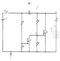
- FIG. 1 is a circuit diagram illustrating a configuration of a latching relay drive circuit 1 according to the first embodiment.
- the latching relay drive circuit 1 includes an operation coil L1 provided in a one-winding latching relay and an internal resistance R5 thereof.
- a capacitor C1 is connected in series to the operation coil L1.
- the latching relay drive circuit 1 is provided with a transistor M2 (first switch element) connected in parallel to the capacitor C1 and the operation coil L1.
- the drain terminal of the transistor M2 is connected to a constant potential, for example, the ground G.
- the latching relay drive circuit 1 has a power source 2 and a switch SW provided for charging the capacitor C1 based on the power source 2 and causing a set current to flow through the operation coil L1.
- a diode D1 is provided between the switch SW and the capacitor C1.
- the capacitor C1 has a plus capacitor terminal corresponding to the plus terminal of the power source 2 and a minus capacitor terminal corresponding to the minus terminal of the power source 2.
- the negative capacitor terminal of the capacitor C1 is connected to the ground G via the operation coil L1 and the internal resistor R5, and is held at a constant potential.
- the latching relay drive circuit 1 has one end coupled to the diode D1, the other end coupled to the gate terminal of the transistor M2, a one end coupled to the gate terminal of the transistor M2, and the other end to the ground G. And a voltage dividing resistor R4 coupled to each other.
- the latching relay drive circuit 1 has a transistor M1 (second switch element) that is turned on when the switch SW is closed and turned off when the switch SW is opened.
- the source terminal of transistor M1 is coupled to the gate terminal of transistor M2.
- the drain terminal of the transistor M2 is connected to the ground G.
- the latching relay drive circuit 1 has one end coupled to the diode D1, the other end coupled to the gate terminal of the transistor M1, a one end coupled to the gate terminal of the transistor M1, and the other end to the ground G. And a voltage dividing resistor R3 coupled to each other.
- the operation coil L1 will be described as having, for example, an inductance of 40 mH and an internal resistance of 40 ohm.
- the capacitance value of the capacitor C1 is determined so that the pulse widths of the set current and the reset current are long enough to operate the latching relay.
- the capacitance value is determined by the following equation.
- C1 3AA / R5
- the voltage dividing resistors R2 and R4 are determined in the same manner as the voltage dividing resistors R1 and R3.
- the gate-source voltage of the transistor M1 becomes lower than the drive voltage and the transistor M1 is turned off.
- the voltage at the point A becomes a voltage obtained by dividing the charging voltage of the capacitor C1 by the voltage dividing resistors R2 and R4, and the transistor M2 is turned on.
- the transistor M2 is turned on, the charge charged in the capacitor C1 is discharged, and a reset current flows through the operation coil L1. That is, the reset current flows from the plus terminal of the capacitor C1 to the minus terminal of the capacitor C1 via the transistor M2 and the operation coil L1.
- the potential of the negative terminal of the capacitor C1 is determined by the ground G and the positive terminal of the capacitor C1 until the transistor M1 is turned off and the transistor M2 is turned on. The terminal is separated from the power supply 2 and the circuit on the switch SW side by a diode D1.
- the voltage at the plus terminal and the minus terminal of the capacitor C1 does not drop while maintaining the potential difference in synchronization with the input voltage Vin, but the voltage at the plus terminal of the capacitor C1 is discharged through the voltage dividing resistor R2. It will go down gradually.
- the voltage drop speed of the positive terminal of the capacitor C1 is determined by a time constant composed of the capacitor C1 and the voltage dividing resistor R2. Therefore, the time constant composed of the capacitor C1 and the voltage dividing resistor R2 is sufficiently long with respect to the voltage drop time of the system at the time of power-off (which varies depending on the system, but is generally 250 msec or shorter). If designed to be (for example, 1 second or longer), it is possible to suppress the discharge of the capacitor until the reset current flows.
- FIG. 2A is a waveform diagram showing the input voltage Vin and the reset current iR in the normal off operation of the latching relay drive circuit 1
- FIG. 2B shows the input voltage Vin and the reset current iR in the off operation when the power is shut off. It is a waveform diagram.
- the peak value of the reset current iR is 213 mA and does not greatly decrease from the peak value of the reset current iR in the normal off operation as in the conventional configuration. Therefore, even if the power is cut off due to a power failure, a sufficient reset current can be supplied to reliably return the one-winding latching relay.
- FIG. 3 is a waveform diagram showing the input voltage Vin in the off operation when the power is cut off and the voltage OutA at the point A in FIG.
- the switch SW is closed at time 20 ms, the power supply is cut off due to a power failure, the input voltage Vin starts to drop from 12 V, and the input voltage Vin reaches zero V at time 270 ms is shown. That is, when the voltage drop time from 12V to zero V of the input voltage Vin is 250 msec (90% -10% fall time is 200 msec), the voltage OutA is steep at 5 msec (10% -90% rise time). respond.
- this 5 msec is a value determined by the input / output characteristics (static characteristics) of the transistor M1. . That is, the rise time of the transistor M1 is determined depending on the performance of the transistor M1.
- the transistor M1 changes sharply even when the power supply is cut off due to a power failure and the voltage drop rate of the input voltage Vin is slow. As a result, the input voltage to the gate terminal of the next-stage transistor M2 also becomes steep, so that the transistor M2 can be switched more steeply.
- FIG. 4 is a graph showing the relationship between the voltage drop time and the reset current peak of the latching relay drive circuit and the conventional drive circuit.
- a line X indicates the relationship between the peak value of the reset current and the voltage drop time by the latching relay drive circuit 1 of the first embodiment.
- a line A1 shows the above-described relationship by the conventional latching relay drive circuit of FIG.
- a line A2 indicates the above-described relationship with another conventional latching relay drive circuit shown in FIG.
- the reset current flows in the same manner as in the conventional case in the normal off operation (voltage drop time 0 msec). And even when the power supply voltage gradually falls due to a power failure or the like (voltage drop time (when the power supply voltage before the power failure is 100%, the time until the power supply voltage drops from 90% to 10%) 200 msec), The latching relay drive circuit 1 has a larger reset current flow than the conventional drive circuit shown in FIGS.
- FIG. 5 is a circuit diagram showing a configuration of a latching relay drive circuit 1A according to the second embodiment.
- the same components as those described in the first embodiment are denoted by the same reference numerals, and detailed description of these components will not be repeated.
- the latching relay drive circuit 1A is provided with an off-delay capacitor C2 connected in parallel with the voltage dividing resistor R3. One end of the off-delay capacitor C2 is coupled to a point B between the voltage dividing resistor R1 and the voltage dividing resistor R3, and the other end is coupled to the ground G.
- FIG. 6 is a waveform diagram for explaining the input voltage and the reset current in the off operation when the power of the latching relay drive circuit 1A is turned off.
- the time from when the power is shut off due to a power failure until the transistor M2 is turned on and the supply of the reset current to the operating coil L1 is set by a time constant determined by the voltage dividing resistors R1 and R3 and the off-delay capacitor C2. Can do.
- the input voltage Vin starts to decrease from 12V due to a power failure at time 1.0sec, and reaches zero V at time 1.25sec.
- the capacitance of the off-delay capacitor C2 is 0.1 ⁇ F
- the reset current iR1 is delayed after 14 msec due to the time constant determined by the voltage dividing resistors R1 and R3 and the off-delay capacitor C2, compared to the case without the off-delay capacitor. Flows.
- the reset current iR2 flows after a delay of 280 msec as compared with the case without the off-delay capacitor due to the time constant determined by the voltage dividing resistors R1 and R3 and the off-delay capacitor C2.
- the reset current iR3 flows after a delay of 3.5 seconds as compared with the case where there is no off-delay capacitor.
- FIG. 7 is a graph showing the relationship between the voltage drop time of the latching relay drive circuit 1A and the conventional drive circuit and the peak of the reset current.
- Line X and lines A1 to A3 are the same as those in FIG.
- Point D1 shows the relationship between the peak of the reset current and the voltage drop time when the off-delay capacitor C2 is 0.1 ⁇ F and delayed by 14 msec.
- Point D2 shows the above relationship when the off-delay capacitor C2 is 1 ⁇ F and delayed by 280 msec.
- Point D3 indicates the above relationship when the off-delay capacitor C2 is 10 ⁇ F and delayed for 3.5 seconds. If the delay time is set excessively, the peak of the reset current decreases as shown at point D3. However, by setting the delay time appropriately, sufficient reset can be performed while providing the delay time as shown at points D1 and D2. A current can be secured.
- the relay turn-off timing can be delayed. Therefore, for example, when the latching relay drive circuit is used as a power supply relay, a necessary operation as a system of the latching relay drive circuit can be performed before the relay is turned off and the power supply to the subsequent circuit is cut off.
- FIG. 8 is a circuit diagram illustrating a configuration of a latching relay drive circuit 1B according to the third embodiment.
- the same components as those described in the first embodiment are denoted by the same reference numerals, and detailed description of these components will not be repeated.
- the latching relay drive circuit 1B has a Schmitt circuit 3.
- a pair of inputs of the Schmitt circuit 3 are coupled to the switch SW and the negative terminal of the power source 2, respectively.
- the pair of outputs of the Schmitt circuit 3 are coupled to the diode D1 and the ground G, respectively.
- the latching relay drive circuit may be combined with the Schmitt circuit.
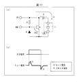
- FIG. 17 is a circuit diagram illustrating a configuration of a latching relay drive circuit 1C according to the fourth embodiment.
- the same components as those described in the first embodiment are denoted by the same reference numerals, and detailed description of these components will not be repeated.
- the latching relay drive circuit 1C includes a comparator U1A, a resistor R6, a resistor R7, a resistor R8, and a transistor U1A instead of the transistor M1, the voltage dividing resistor R1, and the voltage dividing resistor R3 in the latching relay drive circuit 1 according to the first embodiment.
- a zener diode D2 is provided.
- resistor R6 One end of the resistor R6 is coupled to the diode D1 and the switch SW, and the other end of the resistor R6 is coupled to the inverting input terminal of the comparator U1A.
- resistor R7 One end of resistor R7 is coupled to diode D1 and switch SW, and the other end of resistor R7 is coupled to the non-inverting input terminal of comparator U1A.
- One end of the resistor R8 is coupled to the resistor R6 and the inverting input terminal of the comparator U1A, and the other end of the resistor R8 is coupled to the ground G.
- the cathode of the Zener diode D2 is coupled to the resistor R7 and the non-inverting input terminal of the comparator U1A, and the anode of the Zener diode D2 is coupled to the ground G.
- the output terminal of the comparator U1A is connected to the gate terminal of the transistor M2. Also, the positive supply voltage terminal of comparator U1A is coupled to the cathode of diode D1 and capacitor C1, and the negative supply voltage terminal of comparator U1A is coupled to ground G.
- the breakdown voltage Vz of the Zener diode D2 is set to the voltage Vr between the resistor R6 and the resistor R8, that is, the power source voltage.
- the resistance values of the resistors R6 and R8 are set so as to be lower than the voltage Vr divided by the resistors R6 and R8.
- the breakdown voltage Vz is lower than the voltage Vr between the resistor R6 and the resistor R8. It has become. Therefore, since the voltage at the inverting input terminal is higher than the voltage at the non-inverting input terminal of the comparator U1A, the output of the comparator U1A is low and the output voltage is at the ground G level. As a result, the gate of the transistor M2 becomes the ground G level, and the transistor M2 is turned off. As a result, the set current flows from the power source 2 toward the ground G via the switch SW, the diode D1, the capacitor C1, and the operation coil L1.
- the switch SW is opened to change the input voltage Vin from on to off
- the voltage at the non-inverting input terminal of the comparator U1A is maintained at the breakdown voltage Vz of the Zener diode D2, while the voltage at the inverting input terminal of the comparator U1A is maintained.
- the voltage that is, the voltage Vr between the resistor R6 and the resistor R8 decreases as the supplied voltage decreases.
- the breakdown voltage Vz becomes higher than the voltage Vr between the resistors R6 and R8
- the output of the comparator U1A becomes High, and the output voltage becomes the charging voltage of the capacitor C1.
- the transistor M2 is turned on by the output voltage of the comparator U1A.
- the transistor M2 When the transistor M2 is turned on, the charge charged in the capacitor C1 is discharged, and a reset current flows through the operation coil L1. That is, the reset current flows from the plus terminal of the capacitor C1 to the minus terminal of the capacitor C1 via the transistor M2 and the operation coil L1.
- the same operation as that of the latching relay drive circuit 1 according to the first embodiment can also be realized by the latching relay drive circuit 1C according to the fourth embodiment.
- the switch SW may be constituted by a semiconductor switch. Moreover, although the example which has arrange
- Nonpolar capacitors have been described by taking examples of polar capacitors, but the present invention is not limited to this.
- Nonpolar capacitors can also be applied to the present invention.
- Nonpolar capacitors generally have high reliability, but the cost increases as the capacitance increases.
- a polar capacitor having a large capacity is low in cost, but may be constituted by a nonpolar capacitor having high reliability even if the cost is somewhat high.
- the electromagnetic relay of the drive circuit is a type of electromagnetic relay in which the time for passing the reset current (the above-described current pulse width AA necessary for the operation of the latching relay) may be short, the drive circuit can be configured with a nonpolar capacitor. can do.
- the reset current should be evaluated based on the current value and time width required for resetting (pulse width AA of the current required for latching relay operation), but the time width should be designed in any way depending on the capacitance of the capacitor. Therefore, the peak value of the reset current was evaluated. If the peak value of the reset current is small relative to the current required for resetting, resetting cannot be performed no matter how much the capacitance of the capacitor is designed. Further, when the peak value of the reset current is large, there is an advantage that the capacitance of the capacitor satisfying the time width (the necessary current pulse width AA) can be reduced. That is, the smaller the capacitance of the capacitor, the smaller the size and the lower the cost. As described above, since the design factor is to increase the peak value of the reset current, the comparison is made with the prior art based on the peak value of the reset current.
- the voltage dividing resistors R1, R3, or R4 may be changed to a Zener diode. Further, the voltage dividing resistors R1 and R4 may be changed to Zener diodes, and the voltage dividing resistors R3 and R4 may be changed to Zener diodes.
- the transistors M1 and M2 are not limited to FETs (Field-Effect Transistors), but may be configured by other switching elements such as bipolar transistors.
- a latching relay drive circuit includes an operation coil (operation coil L1) provided in a one-winding latching relay, a capacitor (capacitor C1) connected in series to the operation coil, and a power source (power source 2).
- a first switch element drive circuit through which a discharge current of the capacitor to be applied flows, and a discharge current of the capacitor other than the first switch element drive circuit in an opening period of the operation switch or a power supply failure occurrence period from the power source And a discharge inhibiting element (diode D1) that inhibits outflow.
- the latching relay drive circuit in the above configuration, detects the opening of the operation switch or the occurrence of power supply failure from the power source, and discharges the capacitor to the first switch element drive circuit. It is good also as a structure further provided with the detection circuit which changes this 1st switch element drive circuit state so that may flow.
- the first switch element drive circuit is connected in parallel with the first switch element with respect to a series circuit of the operation coil and the capacitor.
- the second voltage dividing circuit includes a pair of second voltage dividing elements (voltage dividing resistors R2 and R4), and between the pair of second voltage dividing elements, The signal input unit of the first switch element and the detection circuit may be connected.
- the detection circuit detects the opening of the operation switch or the occurrence of a power supply failure from the power source, the potential state of the signal input unit of the first switch element is changed by the operation of the detection circuit.
- the discharge current of the capacitor can be input to the signal input portion of the first switch element without being affected by the rate of drop of the voltage supplied from the power supply.
- the detection circuit includes a second switch element (transistor M1), and the signal input unit (gate terminal) of the second switch element is provided.
- a voltage that changes in response to the opening of the operation switch or the occurrence of a power supply failure from the power supply is applied, and the first switch element drive circuit state is changed by the switch operation of the second switch element. It is good also as a structure.
- the speed of the switch operation of the second switch element does not change even when the voltage drop rate supplied from the power source is slow, for example. Therefore, the first switch element drive circuit state can be changed by the switching operation of the second switch element without being affected by the drop rate of the voltage supplied from the power source.
- the detection circuit includes a first voltage divider circuit connected to the power supply via the operation switch, and the first divider
- the voltage circuit includes a pair of first voltage dividing elements (voltage dividing resistors R1 and R3), a signal input section of the second switch element is connected between the pair of first voltage dividing elements, and the operation switch is opened.
- the voltage dividing ratio of the pair of first voltage dividing elements may be determined so that the second switch element is turned on when a power supply failure from the power source occurs.
- the second switch element can be accurately turned on when the operation switch is opened or a power supply failure from the power source occurs.
- the detection circuit includes a comparator (comparator U1A), and the non-inverting input terminal and the inverting input terminal of the comparator A voltage that changes in response to the opening of the operation switch or the occurrence of a power supply failure from the power source may be applied, and the first switch element drive circuit state may be changed by changing the output of the comparator.
- the output change rate of the comparator does not change. Therefore, it is possible to change the state of the first switch element drive circuit by changing the output of the comparator without being affected by the drop rate of the voltage supplied from the power source.
- the second voltage dividing element on the operation switch side of the pair of second voltage dividing elements is a resistor, and a time constant determined by the resistor and the capacitor is 1 It is good also as composition which is more than second.
- the capacitor when the power supply voltage drops while the operation switch is closed, the capacitor is prevented from being discharged before the second switch element is turned off, that is, before the reset current is supplied. Can do. Therefore, a sufficient reset current can be supplied to the operation coil, and the one-winding latching relay can be reliably restored.
- the voltage drop time of the latching relay drive circuit depending on the system, generally 200 milliseconds or It is possible to take a longer time for the electric charge charged in the capacitor to be discharged through the second voltage dividing element (resistor). Accordingly, it is possible to supply a reset current to the operation coil when the second switch element is turned off.
- the latching relay drive circuit according to the present invention is provided with an off-delay capacitor connected in parallel with the first voltage dividing element opposite to the operation switch of the pair of first voltage dividing elements. It is good.
- the present invention can be used for a latching relay drive circuit that drives or turns a single-winding latching relay that operates or returns when an excitation input is applied to a coil and maintains the state even after the excitation input is removed.
Landscapes
- Physics & Mathematics (AREA)
- Electromagnetism (AREA)
- Engineering & Computer Science (AREA)
- Power Engineering (AREA)
- Relay Circuits (AREA)
Abstract
Description
図9は、特許文献1に開示された従来のラッチングリレー駆動回路の構成を示す回路図である。ラッチングリレー駆動回路は、電源51と電流制限抵抗52と電源スイッチ53と負荷55と負荷55を開閉制御するためのハイブリッドリレー54とを備えている。このハイブリッドリレー54は、シュミット回路56の出力端子にラッチングリレーの操作コイル57とコンデンサ58との直列回路が接続されるとともに、この操作コイル57に対する復帰用のトランジスタ59が並列接続されて構成されている。ハイブリッドリレー54には、トランジスタ59のベース抵抗60と、トランジスタ59のオフ動作用のダイオード61とが設けられている。電源スイッチ53と負荷55との間にはラッチングリレーのリレー接点62が設けられている。
まず、電源スイッチ53を閉成すると、電源51からシュミット回路56を介して操作コイル57に通電され、その通電はコンデンサ58の充電完了まで継続する。この操作コイル57に対する通電で、そのリレー接点62がオンし、負荷55に電源51からリレー接点62を介して通電される。上記操作コイル57への通電時に、ダイオード61には順方向の電流が流れる。このため、トランジスタ59のベース・エミッタ間に電位差が発生しないから、このトランジスタ59がオン動作することはなく、操作コイル57に通電される。
図10は、特許文献2に開示された従来の他のラッチングリレー駆動回路の構成を示す回路図である。この他のラッチングリレー駆動回路は、交流電源ACを備えている。交流電源ACの両端にはスイッチSWを介してサージ吸収器ZNが接続される。サージ吸収器ZNの両端に、サージ電流からの保護用の抵抗Rsを介してダイオードブリッジからなる全波整流回路DBが接続されている。
まず、スイッチSWを閉成すると、交流電圧が全波整流回路DBで整流される。整流された電圧は、トランジスタTr71・Tr72、抵抗R71・R72、及び、ツェナーダイオードZDからなる定電圧回路を経てコンデンサC72により平滑される。この直流電圧は抵抗R73・R74により分圧され、抵抗R74の両端の電圧が0.6~0.7Vに達すると、トランジスタTr73がオンする。そして、コンデンサC72の充電電流が図10に示す点aからダイオードD71、コンデンサC71、及び、操作コイルLyを経由して、トランジスタTr73へ向って流れて、ラッチングリレーがセット、即ち、オン動作する。
図11の(a)は従来のラッチングリレー駆動回路の詳細動作を説明するための回路図であり、(b)は上記ラッチングリレー駆動回路に入力される入力信号及びラッチングリレーの操作コイルに流れるコイル電流を示す波形図である。図11の(a)に示す1巻線ラッチングリレーの操作コイルLは、図9のラッチングリレーの操作コイル57に対応する。コンデンサCは、図9のコンデンサ58に対応する。トランジスタTRは、図9のトランジスタ59に対応する。ダイオードD2は図9のダイオード61に対応し、抵抗Rは図9のベース抵抗60に対応する。
(ラッチングリレー駆動回路1の構成)
図1は、実施形態1に係るラッチングリレー駆動回路1の構成を示す回路図である。ラッチングリレー駆動回路1は、1巻線ラッチングリレーに設けられた操作コイルL1とその内部抵抗R5とを備えている。操作コイルL1にはコンデンサC1が直列に接続されている。
ここで、AAは、ラッチングリレーの動作に必要な電流のパルス幅であり、ラッチングリレーの品種により異なる。例えば、AA=10msecの品種とする。パルス幅AAと内部抵抗R5との値を上式に代入すると、C1=3×0.01÷40=0.75mFが目安となる。ここでは、C1=1mFとした。
まず、スイッチSWが閉成されて入力電圧Vinがオフからオンになった瞬間に、分圧抵抗R1・R3により入力電圧Vinが分圧されトランジスタM1がオンする。トランジスタM1がオンすると、トランジスタM2のゲートがトランジスタM1を介してグランドGと接続され、トランジスタM2がオフする。この結果、セット電流は、電源2から、スイッチSW、ダイオードD1、コンデンサC1、操作コイルL1を経由してグランドGに向かって流れる。
図4は、上記ラッチングリレー駆動回路及び従来の駆動回路の電圧降下時間とリセット電流のピークとの関係を示すグラフである。線Xは、実施の形態1のラッチングリレー駆動回路1によるリセット電流のピーク値と電圧降下時間との関係を示している。線A1は、図9の従来のラッチングリレー駆動回路による上記関係を示している。線A2は、図10に示す従来の他のラッチングリレー駆動回路による上記関係を示している。
図5は、実施形態2に係るラッチングリレー駆動回路1Aの構成を示す回路図である。実施の形態1で前述した構成要素と同一の構成要素には同一の参照符号を付し、これらの構成要素について詳細な説明は繰り返さない。
図8は、実施形態3に係るラッチングリレー駆動回路1Bの構成を示す回路図である。実施の形態1で前述した構成要素と同一の構成要素には同一の参照符号を付し、これらの構成要素について詳細な説明は繰り返さない。
図17は、実施形態4に係るラッチングリレー駆動回路1Cの構成を示す回路図である。実施の形態1で前述した構成要素と同一の構成要素には同一の参照符号を付し、これらの構成要素について詳細な説明は繰り返さない。
まず、スイッチSWが閉成されて入力電圧Vinがオフからオンになった瞬間に、コンパレータU1Aの非反転入力端子の電圧は、ツェナーダイオードD2の降伏電圧Vzとなる。一方、コンパレータU1Aの反転入力端子の電圧は、抵抗R6と抵抗R8との間の電圧Vrとなる。
スイッチSWは、半導体スイッチにより構成してもよい。また、スイッチSWを電源2のプラス端子側に配置した例を示したが、本発明はこれに限定されず、スイッチSWは電源2のマイナス端子側に配置してもよい。実施の形態1及び2のラッチングリレー駆動回路1・1Aについても同様である。
本発明の態様に係るラッチングリレー駆動回路は、1巻線ラッチングリレーに設けられた操作コイル(操作コイルL1)と、前記操作コイルに直列に接続されたコンデンサ(コンデンサC1)と、電源(電源2)に基づいて前記コンデンサを充電して前記操作コイルにセット電流を流すために設けられた操作スイッチ(スイッチSW)と、前記操作コイルおよび前記コンデンサの直列回路の両端に並列接続される単一の第1スイッチであって、当該第1スイッチ素子(トランジスタM2)がオンしたときに、該直列回路を含む閉回路を形成して前記コンデンサの放電電流を通過させる単一の第1スイッチ素子と、前記操作スイッチの開成または前記電源からの電力供給障害発生にしたがい、前記第1スイッチ素子の信号入力部(ゲート端子)に印加される前記コンデンサの放電電流が流れる第1スイッチ素子駆動回路と、前記操作スイッチの開成期間または前記電源からの電力供給障害発生期間において、前記コンデンサの放電電流が前記第1スイッチ素子駆動回路以外へ流出することを抑止する放電抑止素子(ダイオードD1)とを備えている。
2 電源
3 シュミット回路
L1 操作コイル
C1 コンデンサ
SW スイッチ
M1 トランジスタ(第2スイッチ素子)
M2 トランジスタ(第1スイッチ素子)
R1、R3 分圧抵抗
R2、R4 分圧抵抗
R6、R7、R8 抵抗
C2 オフディレイコンデンサ
D1 ダイオード
D2 ツェナーダイオード
G グランド(一定電位)
U1A コンパレータ
Claims (9)
- 1巻線ラッチングリレーに設けられた操作コイルと、
前記操作コイルに直列に接続されたコンデンサと、
電源に基づいて前記コンデンサを充電して前記操作コイルにセット電流を流すために設けられた操作スイッチと、
前記操作コイルおよび前記コンデンサの直列回路の両端に並列接続される単一の第1スイッチであって、当該第1スイッチ素子がオンしたときに、前記直列回路を含む閉回路を形成して前記コンデンサの放電電流を通過させる第1スイッチ素子と、
前記操作スイッチの開成または前記電源からの電力供給障害発生にしたがい、前記第1スイッチ素子の信号入力部に印加される前記コンデンサの放電電流が流れる第1スイッチ素子駆動回路と、
前記操作スイッチの開成期間または前記電源からの電力供給障害発生期間において、前記コンデンサの放電電流が前記第1スイッチ素子駆動回路以外へ流出することを抑止する放電抑止素子と
を備えたことを特徴とするラッチングリレー駆動回路。 - 前記操作スイッチの開成または前記電源からの電力供給障害発生を検出し、前記第1スイッチ素子駆動回路に前記コンデンサの放電電流が流れるように該第1スイッチ素子駆動回路状態を変更する検出回路をさらに備えたことを特徴とする請求項1に記載のラッチングリレー駆動回路。
- 前記第1スイッチ素子駆動回路が、前記操作コイルおよび前記コンデンサの直列回路に対して前記第1スイッチ素子と並列に接続された第2分圧回路によって構成されており、
前記第2分圧回路は一対の第2分圧素子を含み、
前記一対の第2分圧素子の間に、前記第1スイッチ素子の信号入力部、および、前記検出回路が接続されることを特徴とする請求項2に記載のラッチングリレー駆動回路。 - 前記検出回路が第2スイッチ素子を備えており、
前記第2スイッチ素子の信号入力部に対して、前記操作スイッチの開成または前記電源からの電力供給障害発生に応じて変化する電圧が印加されており、
前記第2スイッチ素子のスイッチ動作によって、前記第1スイッチ素子駆動回路の状態を変更することを特徴とする請求項2に記載のラッチングリレー駆動回路。 - 前記検出回路が、前記操作スイッチを介して前記電源に接続された第1分圧回路を備えており、
前記第1分圧回路は一対の第1分圧素子を含み、
前記一対の第1分圧素子の間に前記第2スイッチ素子の信号入力部が接続され、
前記操作スイッチの開成または前記電源からの電力供給障害発生時に、前記第2スイッチ素子がオン状態となるように前記一対の第1分圧素子の分圧比が定められていることを特徴とする請求項4記載のラッチングリレー駆動回路。 - 前記検出回路が、コンパレータを備えており、
前記コンパレータの非反転入力端子および反転入力端子に対して、前記操作スイッチの開成または前記電源からの電力供給障害発生に応じて変化する電圧が印加されており、
前記コンパレータの出力変化によって、前記第1スイッチ素子駆動回路状態を変更することを特徴とする請求項2に記載のラッチングリレー駆動回路。 - 操作スイッチを介して電源に接続された第1分圧回路と、
前記第1分圧回路の前記操作スイッチとの接続部からダイオードを介して接続された第2分圧回路と、
前記第2分圧回路と並列に接続された第1スイッチ素子と、
前記第2分圧回路と並列に接続されたLC回路であって、1巻線ラッチングリレーの操作コイル及びコンデンサを含むLC回路とを備え、
前記ダイオードは前記第1分圧回路から前記第2分圧回路に向かって順方向となるように配置され、
前記第1分圧回路は一対の第1分圧素子を含み、
前記第2分圧回路は一対の第2分圧素子を含み、
前記一対の第1分圧素子の間に第2スイッチ素子の信号入力部が接続され、
前記一対の第2分圧素子の間に前記第2スイッチ素子の電流入力部および前記第1スイッチ素子の信号入力部が接続され、
前記第2スイッチ素子の電流出力部が前記電源の前記操作スイッチと反対側に接続され、
前記操作スイッチが閉成すると前記第2スイッチ素子がオン状態となるように前記一対の第1分圧素子の分圧比が定められ、
前記コンデンサに充電された電荷に基づく充電電圧が前記第2分圧回路に印加されると前記第1スイッチ素子がオン状態となるように前記一対の第2分圧素子の分圧比が定められ、
前記操作スイッチが閉成状態から開成状態に切り替わったときに、前記第2スイッチ素子がオン状態からオフ状態に切り替わると共に、前記第1スイッチ素子がオフ状態からオン状態に切り替わり、前記コンデンサに充電された電荷を、前記第1スイッチ素子を介して放電させて前記操作コイルにリセット電流を流すことを特徴とするラッチングリレー駆動回路。 - 前記一対の第2分圧素子のうちの前記操作スイッチ側の第2分圧素子が抵抗であり、
前記抵抗と前記コンデンサとにより定まる時定数が1秒以上であることを特徴とする請求項3または7に記載のラッチングリレー駆動回路。 - 前記一対の第1分圧素子のうちの前記操作スイッチと反対側の第1分圧素子と並列に接続されたオフディレイコンデンサが設けられていることを特徴とする請求項5または7に記載のラッチングリレー駆動回路。
Priority Applications (4)
| Application Number | Priority Date | Filing Date | Title |
|---|---|---|---|
| US15/119,398 US10176950B2 (en) | 2014-03-13 | 2014-12-08 | Latching relay drive circuit |
| JP2016507273A JP6281631B2 (ja) | 2014-03-13 | 2014-12-08 | ラッチングリレー駆動回路 |
| CN201480075221.3A CN105981128B (zh) | 2014-03-13 | 2014-12-08 | 闩锁继电器驱动电路 |
| EP14885537.2A EP3118877B1 (en) | 2014-03-13 | 2014-12-08 | Latching-relay drive circuit |
Applications Claiming Priority (2)
| Application Number | Priority Date | Filing Date | Title |
|---|---|---|---|
| JP2014-050064 | 2014-03-13 | ||
| JP2014050064 | 2014-03-13 |
Publications (1)
| Publication Number | Publication Date |
|---|---|
| WO2015136797A1 true WO2015136797A1 (ja) | 2015-09-17 |
Family
ID=54071262
Family Applications (1)
| Application Number | Title | Priority Date | Filing Date |
|---|---|---|---|
| PCT/JP2014/082401 Ceased WO2015136797A1 (ja) | 2014-03-13 | 2014-12-08 | ラッチングリレー駆動回路 |
Country Status (5)
| Country | Link |
|---|---|
| US (1) | US10176950B2 (ja) |
| EP (1) | EP3118877B1 (ja) |
| JP (1) | JP6281631B2 (ja) |
| CN (1) | CN105981128B (ja) |
| WO (1) | WO2015136797A1 (ja) |
Cited By (1)
| Publication number | Priority date | Publication date | Assignee | Title |
|---|---|---|---|---|
| JP2022507254A (ja) * | 2018-11-13 | 2022-01-18 | フェニックス コンタクト ゲーエムベーハー ウント コムパニー カーゲー | 制御回路 |
Families Citing this family (7)
| Publication number | Priority date | Publication date | Assignee | Title |
|---|---|---|---|---|
| CN107452547B (zh) * | 2016-06-01 | 2020-07-10 | 中兴通讯股份有限公司 | 单线圈磁保持继电器控制电路及方法 |
| TWI632580B (zh) * | 2017-04-18 | 2018-08-11 | 徐政村 | 電源開關模組 |
| CA3072812A1 (en) | 2017-08-18 | 2019-02-21 | Sensus Spectrum, Llc | Method to detect operational state of remote disconnect latching relay |
| US11004637B2 (en) * | 2018-03-22 | 2021-05-11 | Rosemount Inc. | Field device latching relay reset |
| CN110911193B (zh) * | 2019-11-04 | 2024-12-03 | 深圳市纽尔科技有限公司 | 机械开关电路结构及设置方法 |
| EP4111275B1 (en) | 2020-02-27 | 2024-12-04 | Parker-Hannifin Corporation | System and method for controlling a latching relay failsafe |
| CN111403238B (zh) * | 2020-03-04 | 2022-02-15 | 厦门华联电子股份有限公司 | 继电器的驱动电路 |
Citations (3)
| Publication number | Priority date | Publication date | Assignee | Title |
|---|---|---|---|---|
| JPS54130872A (en) * | 1978-04-03 | 1979-10-11 | Matsushita Electric Works Ltd | Bistable relay driving circuit |
| JPS61178241U (ja) * | 1985-04-24 | 1986-11-07 | ||
| JPH0251817A (ja) * | 1988-08-12 | 1990-02-21 | Matsushita Electric Works Ltd | リレーの駆動回路 |
Family Cites Families (8)
| Publication number | Priority date | Publication date | Assignee | Title |
|---|---|---|---|---|
| DE2747607C2 (de) * | 1977-10-24 | 1991-05-08 | Sds-Elektro Gmbh, 8024 Deisenhofen | Schaltungsanordnung zur Ansteuerung eines bistabilen Relais |
| JPS58137931A (ja) | 1982-02-10 | 1983-08-16 | 松下電工株式会社 | オフデイレ−型リレ−の駆動回路 |
| JPS6255826A (ja) * | 1985-09-03 | 1987-03-11 | オムロン株式会社 | 電磁リレ−の駆動回路 |
| US6021038A (en) * | 1998-08-27 | 2000-02-01 | Hanchett Entry Systems, Inc. | Control circuit for an electric door strike using a latching solenoid |
| DE502008000959D1 (de) * | 2008-06-18 | 2010-08-26 | Sma Solar Technology Ag | Schaltungsanordnung mit einem bistabilen Relais zwischen einem Netz und einem Wechselrichter |
| CN201490100U (zh) * | 2009-08-13 | 2010-05-26 | 合肥钦力电子有限公司 | Pwm脉宽调制的接触器线圈驱动电路 |
| US9076616B2 (en) * | 2013-01-30 | 2015-07-07 | Raritan Inc. | Methods and apparatus for improved latching relay driver |
| CN203456389U (zh) * | 2013-08-23 | 2014-02-26 | 艾默生电气公司 | 一种继电器驱动电路 |
-
2014
- 2014-12-08 WO PCT/JP2014/082401 patent/WO2015136797A1/ja not_active Ceased
- 2014-12-08 EP EP14885537.2A patent/EP3118877B1/en active Active
- 2014-12-08 CN CN201480075221.3A patent/CN105981128B/zh active Active
- 2014-12-08 US US15/119,398 patent/US10176950B2/en active Active
- 2014-12-08 JP JP2016507273A patent/JP6281631B2/ja active Active
Patent Citations (3)
| Publication number | Priority date | Publication date | Assignee | Title |
|---|---|---|---|---|
| JPS54130872A (en) * | 1978-04-03 | 1979-10-11 | Matsushita Electric Works Ltd | Bistable relay driving circuit |
| JPS61178241U (ja) * | 1985-04-24 | 1986-11-07 | ||
| JPH0251817A (ja) * | 1988-08-12 | 1990-02-21 | Matsushita Electric Works Ltd | リレーの駆動回路 |
Cited By (1)
| Publication number | Priority date | Publication date | Assignee | Title |
|---|---|---|---|---|
| JP2022507254A (ja) * | 2018-11-13 | 2022-01-18 | フェニックス コンタクト ゲーエムベーハー ウント コムパニー カーゲー | 制御回路 |
Also Published As
| Publication number | Publication date |
|---|---|
| US10176950B2 (en) | 2019-01-08 |
| EP3118877A1 (en) | 2017-01-18 |
| JP6281631B2 (ja) | 2018-02-21 |
| EP3118877A4 (en) | 2017-11-01 |
| CN105981128B (zh) | 2017-12-29 |
| CN105981128A (zh) | 2016-09-28 |
| EP3118877B1 (en) | 2020-03-11 |
| US20170062163A1 (en) | 2017-03-02 |
| JPWO2015136797A1 (ja) | 2017-04-06 |
Similar Documents
| Publication | Publication Date | Title |
|---|---|---|
| JP6281631B2 (ja) | ラッチングリレー駆動回路 | |
| US8472216B2 (en) | Circuit arrangement and control circuit for a power-supply unit, computer power-supply unit and method for switching a power-supply unit | |
| JP6360168B2 (ja) | ダイオード接点保護複合スイッチの制御回路及びリレーの制御方法 | |
| US11011903B2 (en) | Disconnecting device | |
| US9979286B2 (en) | Power converting device | |
| US7403366B2 (en) | Control circuit for an electromagnetic drive | |
| JP2003338239A (ja) | ハイブリッド直流電磁接触器 | |
| US9871369B2 (en) | Load driver circuit and load short-circuit detection circuit | |
| WO2012140840A1 (ja) | コンバータ装置及び半導体装置 | |
| JP6237952B2 (ja) | 内部電源回路および半導体装置 | |
| KR20120091134A (ko) | 프리휠링 회로 | |
| US7123462B2 (en) | Load control device | |
| US7369391B2 (en) | Drive circuit of direct-current voltage-driven magnetic contactor and power converter | |
| US9870889B2 (en) | Circuit arrangement for actuating a bistable relay | |
| JP7036033B2 (ja) | アーク抑制装置 | |
| US11189438B2 (en) | Arc suppression device, mobile body, and power supply system | |
| CN112068633A (zh) | 浪涌电流保护电路和固态继电器 | |
| JP2020036307A (ja) | 過電圧抑制回路及び直流遮断装置 | |
| JP3564694B2 (ja) | 突入電流抑止装置 | |
| US20210313131A1 (en) | Relay module | |
| JP2017153179A (ja) | スイッチング電源装置 | |
| EP3503394B1 (en) | Discharge circuit for capacitor | |
| CN104078928A (zh) | 电路断路器的欠电压跳闸装置和过欠电压跳闸装置 | |
| CN108963981B (zh) | 分励脱扣器及断路器 | |
| JP2025040671A (ja) | スイッチ装置 |
Legal Events
| Date | Code | Title | Description |
|---|---|---|---|
| 121 | Ep: the epo has been informed by wipo that ep was designated in this application |
Ref document number: 14885537 Country of ref document: EP Kind code of ref document: A1 |
|
| REEP | Request for entry into the european phase |
Ref document number: 2014885537 Country of ref document: EP |
|
| WWE | Wipo information: entry into national phase |
Ref document number: 15119398 Country of ref document: US Ref document number: 2014885537 Country of ref document: EP |
|
| ENP | Entry into the national phase |
Ref document number: 2016507273 Country of ref document: JP Kind code of ref document: A |
|
| NENP | Non-entry into the national phase |
Ref country code: DE |