WO2015137017A1 - 非接触電圧計測装置 - Google Patents
非接触電圧計測装置 Download PDFInfo
- Publication number
- WO2015137017A1 WO2015137017A1 PCT/JP2015/053148 JP2015053148W WO2015137017A1 WO 2015137017 A1 WO2015137017 A1 WO 2015137017A1 JP 2015053148 W JP2015053148 W JP 2015053148W WO 2015137017 A1 WO2015137017 A1 WO 2015137017A1
- Authority
- WO
- WIPO (PCT)
- Prior art keywords
- electrode
- electric field
- field shield
- probe
- voltage
- Prior art date
- Legal status (The legal status is an assumption and is not a legal conclusion. Google has not performed a legal analysis and makes no representation as to the accuracy of the status listed.)
- Ceased
Links
Images


Classifications
-
- G—PHYSICS
- G01—MEASURING; TESTING
- G01R—MEASURING ELECTRIC VARIABLES; MEASURING MAGNETIC VARIABLES
- G01R15/00—Details of measuring arrangements of the types provided for in groups G01R17/00 - G01R29/00, G01R33/00 - G01R33/26 or G01R35/00
- G01R15/14—Adaptations providing voltage or current isolation, e.g. for high-voltage or high-current networks
- G01R15/16—Adaptations providing voltage or current isolation, e.g. for high-voltage or high-current networks using capacitive devices
- G01R15/165—Adaptations providing voltage or current isolation, e.g. for high-voltage or high-current networks using capacitive devices measuring electrostatic potential, e.g. with electrostatic voltmeters or electrometers, when the design of the sensor is essential
-
- G—PHYSICS
- G01—MEASURING; TESTING
- G01R—MEASURING ELECTRIC VARIABLES; MEASURING MAGNETIC VARIABLES
- G01R1/00—Details of instruments or arrangements of the types included in groups G01R5/00 - G01R13/00 and G01R31/00
- G01R1/02—General constructional details
- G01R1/06—Measuring leads; Measuring probes
- G01R1/067—Measuring probes
- G01R1/07—Non contact-making probes
Definitions
- the present invention relates to a non-contact voltage measuring device that measures an AC voltage flowing through a conductor without contacting the conductor.
- a non-contact voltage measuring device includes a probe and an electric circuit.
- a probe When a probe is brought close to a wiring so that a coupling capacitance is generated between the probe and the wiring, the electric circuit is passed through the probe.
- the voltage to be measured is derived based on the voltage signal input to.
- An electric field shield for blocking an external electric field is arranged around the electric circuit.
- the probe and the wiring are closer, the capacitance value of the coupling capacitance increases, and the measurement accuracy of the measurement target voltage is improved. Therefore, it is desirable that the probe is arranged as close as possible to the surface of the wiring. Moreover, it is desirable that the non-contact voltage measuring device can measure the measurement target voltages of various wirings having different diameters.
- the probe can be configured to be deformable so that the probe and the wiring can be sufficiently brought close to each other regardless of the diameter of the wiring.
- Patent Documents 1 to 3 do not disclose a probe that can be deformed according to the shape of the wiring. Therefore, in the non-contact voltage measuring devices described in Patent Documents 1 to 3, the capacitance value of the coupling capacitance is reduced depending on the shape of the wiring, and as a result, the measurement accuracy of the measurement target voltage may be reduced. .
- the present invention has been made in view of the above, and an object of the present invention is to provide a non-contact voltage measuring device capable of measuring a voltage to be measured of various conducting wires having different shapes with a certain accuracy.
- a non-contact voltage measuring device includes a probe, and the probe is connected to the conductor so that a coupling capacitance is generated between the electrode of the probe and the conductor.
- a non-contact voltage measuring device for measuring a voltage to be measured applied to the conductor based on a voltage signal input to the electric circuit via the probe when approaching in a non-contact manner, at least the electric circuit An electric field shield that blocks an electric field incident on the electric circuit by covering a part thereof, and the probe is deformed according to the shape of the conductor and is generated between the electrode and the electric field shield.
- the capacitance value of the parasitic capacitance is kept constant.
- the electrode provided in the probe can be deformed.
- the electrode may be able to be deformed so as to be in close contact with the outer wire coating of the conducting wire (conductor).
- the probe maintains a constant capacitance value of the parasitic capacitance generated between the electrode and the electric field shield even when the electrode is deformed.
- the influence of the parasitic capacitance generated between the electrode of the probe and the electric field shield on the measurement accuracy of the measurement target voltage is eliminated by calibration.
- the conventional configuration as the degree of deformation of the electrode changes, the distance between the electrode and the electric field shield also changes, and as a result, the capacitance value of the parasitic capacitance generated between the electrode and the electric field shield also increases. Change. Therefore, the conventional configuration has a problem that the measurement accuracy of the voltage to be measured changes depending on the degree of deformation of the electrode.
- measurement target voltages of various conductors having different shapes can be measured with a certain accuracy.
- (A) is a graph which shows the electric potential in the range shown with the broken line in (a) of FIG. 4
- (b) is a graph which shows the electric potential in the range shown with the broken line in (b) of FIG.
- (A) is a contour plot which shows the result of having simulated the electric field which generate
- (b) is the electric field which generate
- (A) is a graph which shows the electric field in the range shown with the broken line in (a) of FIG.
- (b) is a graph which shows the electric field in the range shown with the broken line in (b) of FIG. It is an external view which shows the structure of the non-contact voltage measuring device which concerns on Embodiment 2 of this invention. It is a figure which shows the relationship between coupling capacity
- Embodiment 1 Hereinafter, embodiments of the present invention will be described in detail with reference to FIGS.
- FIG. 1 is an external view of the voltage measuring apparatus 1.
- FIG. 2 is a schematic diagram showing the configuration of the voltage measuring apparatus 1.
- the voltage measuring device 1 is a measurement target voltage that is a voltage of alternating current (frequency: f) flowing through a conductor in a wiring w (primary wiring, conductor) having various diameters (for example, ⁇ 11 (mm) to ⁇ 16 (mm)). V L can be measured without contact with the conductor.
- the voltage measuring apparatus 1 includes a detection probe 11 (probe), an electric field shield 12, a lead-out unit 13, and an electric circuit EC.
- the detection probe 11 that is a sensor for the measurement target voltage VL includes two detection electrodes (an inner electrode 11A (first electrode) and an outer electrode 11B (second electrode)).
- the inner electrode 11 ⁇ / b> A and the outer electrode 11 ⁇ / b> B are electrically connected via the connection portion 20.
- the outer electrode 11B is fixed to the electric field shield 12.
- the inner electrode 11A and the outer electrode 11B and the electric field shield 12 are insulated from each other.
- the inner electrode 11A which is a movable electrode, is composed of two leaf springs. A wiring w is arranged between the two leaf springs. The two leaf springs are in close contact with the wiring w by gripping the wiring w. The inner electrode 11A can be elastically deformed so as to be in close contact with the wiring w in accordance with the diameter of the wiring w. The more inner electrode 11A adjacent to the wiring w, the capacitance value of the coupling capacitance C L which is generated between the inner electrode 11A and the wiring w increases.
- An induced voltage is induced in the inner electrode 11A by an alternating current flowing in the wiring w. Further, the same induced voltage as that of the inner electrode 11A is also induced in the outer electrode 11B connected to the inner electrode 11A via the connection portion 20.
- the induced voltage (input voltage V in ) generated in the inner electrode 11A and the outer electrode 11B is input to an electric circuit EC (see FIG. 2) electrically connected to the outer electrode 11B.
- the voltage measuring device 1 further includes resin structures 30, 40, and 50 (see FIG. 4A). These resin structures 30, 40, 50 have a role of holding the wiring w, the outer electrode 11B, the connection portion 20, or the like.
- FIG. 3 is a contour plot diagram showing the result of simulating the electric field generated in the voltage measuring apparatus 1.
- a predetermined potential with the potential of the electric field shield 12 as a reference (0 V) was applied to the inner electrode 11A and the outer electrode 11B.
- the electric field generated by the wiring w is not considered.
- the electric field strength between the inner electrode 11A and the electric field shield 12 is smaller than the electric field strength between the outer electrode 11B and the electric field shield 12. The reason is that the electric field generated by the inner electrode 11 ⁇ / b> A is shielded by the outer electrode 11 ⁇ / b> B disposed between the inner electrode 11 ⁇ / b> A and the electric field shield 12.
- the capacitance value of the parasitic capacitance generated between the inner electrode 11A and the electric field shield 12 is smaller than the capacitance value of the parasitic capacitance generated between the outer electrode 11B and the electric field shield 12. Therefore, the capacitance value of the parasitic capacitance C ppL generated between the detection probe 11 and the electric field shield 12 mostly depends only on the capacitance value of the parasitic capacitance generated between the outer electrode 11B and the electric field shield 12.
- the electric circuit EC as an input voltage V in at the input point p1, to obtain the induced induced voltage in the detection probe 11 (the inner electrode 11A and the outer electrode 11B).
- the electric circuit EC outputs the voltage at the detection point p2 set in the electric circuit EC to the derivation unit 13 as the output voltage Vout .
- the electric circuit EC includes a high impedance part HI having a relatively high impedance value and a low impedance part LOW having a relatively low impedance value. Details of the electric circuit EC will be described later.
- the electric field shield 12 blocks the electric field incident on the electric circuit EC, thereby preventing capacitive coupling between the electric circuit EC and a voltage source other than the wiring.
- the electric field shield 12 may be made of metal (shield metal).
- the electric field shield 12 includes a shield upper part 12A and a shield lower part 12B.
- the outer electrode 11B of the detection probe 11 is fixed inside the shield upper portion 12A.
- the shield lower part 12B can be attached to and detached from the shield upper part 12A.
- the user attaches the shield lower part 12B to the shield upper part 12A after the inner electrode 11A grips the wiring w. Further, the user can replace the wiring w held by the inner electrode 11A with another wiring by removing the shield lower part 12B.
- the electric field shield 12 includes a first electric field shield portion that covers a portion of the electric circuit EC (high impedance portion HI) that is equipotential with the input point p1, and a portion of the electric circuit EC that is equipotential with the detection point p2. And a second electric field shield part covering the low impedance part LOW). In this configuration, the first electric field shield part and the second electric field shield part are insulated.
- a parasitic capacitance C ppL is generated between the electric field shield 12 and the high impedance portion HI. Further, a parasitic capacitance C p is generated between the electric field shield 12 and the low impedance part LOW.
- the deriving unit 13 derives the measurement target voltage V L based on the output voltage V out output from the electric circuit EC. Specifically, the deriving unit 13 derives the measurement target voltage V L according to the following equation.
- V out1 and V out2 mean the output voltage V out when the electric circuit EC is in the first state and the second state (described later), respectively.
- ⁇ 2 ⁇ f (f is the frequency of alternating current flowing in the wiring).
- the parasitic capacitance C p 0. As described below, the parasitic capacitance C p is invalidated by the operational amplifier 15.
- the electric circuit EC includes capacitors C 1 and C 2 , a detection resistor R 1 , a changeover switch 14, and an operational amplifier 15.
- capacitors C 1, C 2 both are connected to the input point p1 to the input voltage V in from the detecting probe 11 is input.
- the detection resistor R 1 is attached between the capacitors C 1 and C 2 and the reference potential point GND.
- the detection point p2 described above is located between the capacitors C 1 and C 2 and the detection resistor R 1 .
- the input voltage V in input from the detection probe 11 to the electric circuit EC is divided into capacitors C 1 and C 2 and a detection resistor R 1 .
- the output voltage V out is equal to the partial pressure of the input voltage V in applied to the detection resistor R 1.
- the capacitance values of the capacitors C 1 and C 2 and the resistance value of the detection resistor R 1 are determined so that the output voltage V out is sufficiently small.
- Changeover switch 14 an electric circuit EC, (i) the capacitor C 1 has a first state in series connected between the coupling capacitance C L and the detection resistor R 1, (ii) the capacitor C 1 and capacitor C 2 Is switched between the second state connected in series between the coupling capacitor C L and the detection resistor R 1 .
- the input voltage V in includes a detection resistor R 1, is divided between the capacitor C 1.
- the detection resistor R 1 is divided between the capacitors C 1 and capacitor C 2.
- the changeover switch 14 an electric circuit EC, (i) the capacitor C 1 is the coupling capacitance C L and the first state of being connected in series between the detection resistor R 1, it is (ii) a capacitor C 2, coupling capacitor C L and a second state connected in series between the detection resistor R 1, may be configured to switch between.
- This configuration for example, in an electric circuit EC, between the input point p1 and the capacitor C 1, and, between the input point p1 and the capacitor C 2, respectively, be provided with a switch which can be switched on and off Can be realized.
- a portion having the same potential as the input point p1 in the electric circuit EC is referred to as a high impedance portion HI.
- a portion having the same potential as the detection point p2 is referred to as a low impedance portion LOW.
- the operational amplifier 15 connects between the low impedance part LOW and the electric field shield 12 in the electric circuit EC.
- the operational amplifier 15 functions to make the electric field shield 12 and the low impedance part LOW have the same potential. This is a so-called driven shield circuit technique.
- the operational amplifier 15 causes the low impedance part LOW and the electric field shield 12 to be at the same potential. Therefore, the low impedance section LOW, no current flows through the parasitic capacitance C p which occurs between the electric field shield 12. Therefore, it is possible to eliminate the possibility of parasitic capacitance C p affects the detected value of the output voltage V out.
- a voltage equal to the voltage (output voltage V out ) in the low impedance part LOW is generated from the voltage (input voltage V in ) in the high impedance part HI, and the generated voltage is the electric field shield 12. May be applied.
- the voltage measuring device 1 does not have to include the operational amplifier 15.
- the electromagnetic field outside the outer electrode 11B that is, the electromagnetic field generated between the outer electrode 11B and the electric field shield 12 depends only on the electric field generated by the outer electrode 11B, and the electric field generated by the inner electrode 11A. Not affected. Therefore, even when the inner electrode 11A is deformed and the electric field generated by the inner electrode 11A changes, the electromagnetic field generated between the outer electrode 11B and the electric field shield 12 does not change.
- the potential of the inner electrode 11A and the outer electrode 11B was set to 1V.
- the electric potential of the wiring w and the electric field shield 12 was set to 0V.
- the diameter of the wiring w was set to 14.4 (phi) (14.4.mm) and 9.4 (phi) (9.4mm), and the electric potential and electric field in the voltage measuring device 1 were calculated under each setting.
- the shape of the inner electrode 11A adjacent to the wiring w changes according to the diameter of the wiring w.
- the voltage measuring device 9 includes only one electrode 91 corresponding to the inner electrode 11A of the voltage measuring device 1. That is, the voltage measuring device 1 is different from the voltage measuring device 1 in that the outer electrode 11B is not provided (see FIG. 4B).
- FIG. 4A and 4B are contour plot diagrams showing the results of simulating the potential generated in the voltage measuring apparatus 1.
- FIG. 4A the left diagram shows the potential when the diameter of the wiring w is 14.4 ⁇ (14.4 mm), and the right diagram shows the diameter of the wiring w 9.4 ⁇ ( 9.4 mm) represents the potential.
- FIG. 4B is a contour plot showing the result of simulating the potential generated in the voltage measuring device 9.
- the interval and shape of the equipotential lines do not depend on the diameter of the wiring w. In other words, the interval and shape of equipotential lines between the outer electrode 11B and the electric field shield 12 do not depend on the shape of the inner electrode 11A.
- FIG. 5 is a graph showing the potential (V) in the range (from the outer electrode 11B to the shield upper part 12A) indicated by a broken line in FIG.
- FIG. 5B is a graph showing the potential (V) in the range indicated by the broken line in FIG.
- the range indicated by the broken line in FIG. 5A corresponds to the range indicated by the broken line in FIG. 5B in the voltage measuring device 9.
- the potential (V) is high in the wiring w in the range from the position (0 mm) of the outer electrode 11 ⁇ / b> B to the position (6 mm) of the shield upper part 12 ⁇ / b> A. It does not depend on the diameter. That is, the height of the potential (V) in this range does not depend on the shape of the inner electrode 11A.
- the height of the potential (V) depends on the shape of the inner electrode 11A in the same range (0 mm to 6 mm).
- FIG. 6A is a contour plot diagram showing the result of simulating the electric field generated in the voltage measuring apparatus 1.
- FIG. 6B is a contour plot showing the result of simulating the electric field generated in the voltage measuring device 9.
- the interval and shape of equipotential lines between the outer electrode 11B and the electric field shield 12 do not depend on the shape of the inner electrode 11A.
- FIG. 7A is a graph showing the electric field (V / m) in the range (from the outer electrode 11B to the shield upper part 12A) indicated by a broken line in FIG.
- FIG. 7B is a graph showing the electric field (V / m) in the range indicated by the broken line in FIG.
- the range indicated by the broken line in FIG. 7A corresponds to the range indicated by the broken line in FIG.
- the strength of the electric field (V / m) depends on the shape of the inner electrode 11A in the same range (0 mm to 6 mm).
- the strength of the coupling between the electric field shield 12 and the outer electrode 11B is constant regardless of the shape of the inner electrode 11A. I understand that. This means that the capacitance value of the parasitic capacitance C ppL generated between the detection probe 11 and the electric field shield 12 does not change even when the inner electrode 11A is deformed.
- the configuration of the detection probe 11 including the outer electrode 11B fixed to the electric field shield 12 is described separately from the inner electrode 11A that is deformed according to the thickness of the wiring w (see FIG. 1). ).
- the detection probe includes only one electrode, and this electrode can be deformed or moved while keeping the capacitance value of the parasitic capacitance C ppL generated between the detection probe and the electric field shield constant. It may be configured.
- FIG. 8 is an external view showing a configuration of the detection probe 21 according to the present embodiment.
- the detection probe 21 includes a clamp part 250 (deformation part) composed of two arms (a first arm 250A and a second arm 250B).
- the clamp part 250 can grip various wirings w having different diameters between the first arm 250A and the second arm 250B.
- the first arm 250A and the second arm 250B are connected to each other by a connecting portion 260.
- the connecting part 260 may be a coil spring, for example.
- the first arm 250A and the second arm 250B can rotate with the connecting portion 260 as a fulcrum.
- the connecting portion 260 applies a force acting in a direction to reduce the distance between the first arm 250A and the second arm 250B to the first arm 250A and the second arm 250B.
- the first arm 250A and the second arm 250B are provided with an electrode 211 and an electric field shield 212, respectively.
- the two electrodes 211 are electrically connected. Both of the two electric field shields 212 are connected to a reference potential point (GND).
- the electrode 211 and the electric field shield 212 may be disposed on either the first arm 250A or the second arm 250B.
- the electrode 211 disposed on the first arm 250A and the second arm 250B is close to the wiring w. Therefore, a coupling capacitance CL is generated between the electrode 211 and the wiring w. An induced voltage is induced in the electrode 211 by an alternating current flowing in the wiring w.
- At least one of the first arm 250A and the second arm 250B includes an electric circuit EC (see FIG. 2) covered with the electric field shield 212.
- the electrode 211 and the electric circuit EC are electrically connected, induced voltage generated in the electrode 211, as the input voltage V in, input to the electric circuit EC.
- Electrical circuit EC outputs the output voltage V out is the partial pressure of the input voltage V in applied to the detection resistor R 1, the deriving unit 13 (see FIG. 2).
- the deriving unit 13 derives the measurement target voltage V L based on the output voltage V out output from the electric circuit EC.
- leading-out part 13 may exist in the inside of the detection probe 21, and may exist in the exterior.
- the electrode 211 and the electric field shield 212 are disposed on the first arm 250A and the second arm 250B. Therefore, even if the first arm 250A and the second arm 250B move according to the diameter of the wiring w gripped by the clamp part 250, the relative position between the electrode 211 and the electric field shield 212 is constant. To maintain. Precisely, the relative position between the electrode 211 and the electric field shield 212 arranged on the first arm 250A, and the relative position between the electrode 211 and the electric field shield 212 arranged on the second arm 250B. The respective positions are kept constant.
- the capacitance value of the parasitic capacitance C ppL generated between the electrode 211 and the electric field shield 212 is kept constant.
- the measurement target voltage V L is expressed by the following mathematical formula.
- the current output to the derivation unit 13 is I 1
- the output voltage is V out1
- the derivation unit The current output to 13 is I 2
- the output voltage is V out2 .
- the capacitance value of the capacitor C 2 is sufficiently larger than the capacitance value of the capacitor C 1 (C 1 ⁇ C 2 ).
- the non-contact voltage measuring device includes a probe, and the probe is contacted with the conductor so that a coupling capacitance is generated between the electrode of the probe and the conductor.
- a non-contact voltage measuring device that measures a voltage to be measured applied to the conductor based on a voltage signal that is input to the electric circuit via the probe when being brought close to each other, covers at least a part of the electric circuit
- the electric field shield for blocking the electric field incident on the electric circuit is provided, the probe is deformed according to the shape of the conductor, and the parasitic capacitance generated between the electrode and the electric field shield is reduced. Keep the capacitance value constant.
- the electrode provided in the probe can be deformed.
- the electrode may be able to be deformed so as to be in close contact with the outer wire coating of the conducting wire (conductor).
- the probe maintains a constant capacitance value of the parasitic capacitance generated between the electrode and the electric field shield even when the electrode is deformed.
- the influence of the parasitic capacitance generated between the electrode of the probe and the electric field shield on the measurement accuracy of the measurement target voltage is eliminated by calibration.
- the conventional configuration as the degree of deformation of the electrode changes, the distance between the electrode and the electric field shield also changes, and as a result, the capacitance value of the parasitic capacitance generated between the electrode and the electric field shield also increases. Change. Therefore, the conventional configuration has a problem that the measurement accuracy of the voltage to be measured changes depending on the degree of deformation of the electrode.
- the probe has a first electrode that can be deformed according to the shape of the conductor and a second electrode that holds a relative position with respect to the electric field shield.
- the first electrode and the second electrode are electrically connected, and the second electrode generates an electric field generated between the first electrode and the electric field shield. You may arrange
- the second electrode of the probe maintains a relative position with respect to the electric field shield.
- the first electrode of the probe is deformed according to the shape of the conductor.
- the total amount of leakage current flowing through the parasitic capacitance generated between the second electrode and the electric field shield is constant regardless of the degree of deformation of the first electrode.
- the second electrode is arranged at a position where the electric field generated between the first electrode and the electric field shield can be shielded. Therefore, no leakage current flows through the parasitic capacitance generated between the first electrode and the electric field shield, so the total amount of leakage current flowing between the probe and the electric field shield is reduced, and the measurement accuracy of the measurement target voltage is improved. To do.
- the non-contact voltage measuring device may be configured such that the distance from the second electrode to the electric field shield is closer than the distance from the first electrode to the electric field shield.
- the capacitance value of the parasitic capacitance generated between the first electrode and the electric field shield is smaller than the capacitance value of the parasitic capacitance generated between the second electrode and the electric field shield. Therefore, the ratio of the capacitance value of the parasitic capacitance generated between the first electrode and the electric field shield in the entire capacitance value of the parasitic capacitance generated between the probe and the electric field shield is reduced. Therefore, when the value of the parasitic capacitance generated between the first electrode and the electric field shield changes, the influence of the change on the measurement accuracy of the measurement target voltage can be suppressed.
- the probe includes a deformable portion that can be deformed according to the shape of the conductor, and the deformable portions are connected to each other by a connecting portion.
- the arm includes a plurality of arms that pivot about the connecting portion, and at least one of the plurality of arms includes the electrode and the electric field shield that are spaced apart by a certain distance. Also good.
- the electrode and the electric field shield are arranged on the arm provided with the deforming portion that deforms according to the shape of the conductor.
- the arm of the deforming portion moves. Since the electrode and the electric field shield are spaced apart from each other by a certain distance on the same arm, the electrode can maintain a relative position with respect to the electric field shield when the arm moves.
- the amount of leakage current flowing through the parasitic capacitance generated between the electrode and the electric field shield does not change. Therefore, the voltage to be measured can be measured with a certain accuracy regardless of the amount of movement of the arm.
- the present invention can be used in a voltage measuring device that measures an AC voltage flowing through a conductive wire in an insulating-coated wiring without contacting the conductive wire.
- Non-contact voltage measuring device 11 Detection probe (probe) 21 Detection probe (probe) 211 electrode 11A inner electrode (first electrode) 11B outer electrode (second electrode) 12 Electric field shield 212 Electric field shield 250 Clamp part (deformation part) 250A First arm (arm) 250B Second arm (arm) 260 connecting part
Landscapes
- Physics & Mathematics (AREA)
- General Physics & Mathematics (AREA)
- Measuring Instrument Details And Bridges, And Automatic Balancing Devices (AREA)
- Measurement Of Current Or Voltage (AREA)
Abstract
形状が異なる様々な導線の計測対象電圧を一定の精度で計測することができる非接触電圧計測装置を提供する。配線wの形状に応じて変形する内側電極(11A)と、電界シールド(12)に対して固定された外側電極(11B)とが、接続部(20)を介して電気的に接続される。
Description
本発明は、導体を流れる交流の電圧を、導体に接触することなく計測する非接触電圧計測装置に関する。
従来、絶縁被覆された配線内の導線を流れる交流の電圧(計測対象電圧)を、導線に接触することなく計測する非接触電圧計測装置が開示されている。
一般的に、非接触電圧計測装置は、プローブおよび電気回路を備えており、プローブと配線との間に結合容量が発生するように、プローブを配線に近接させたとき、プローブを介して電気回路に入力される電圧信号に基づいて、計測対象電圧を導出する。電気回路の周囲には、外部の電界を遮断するための電界シールドが配置される。
一般的に、プローブと配線とが近接するほど、結合容量の容量値が増大し、計測対象電圧の計測精度が向上する。そのため、プローブは、配線の表面にできるだけ近接するように配置されることが望ましい。また、非接触電圧計測装置は、径の太さが異なる様々な配線の計測対象電圧を計測できることが望ましい。
しかしながら、従来の非接触電圧計測装置では、配線の径の太さによって、プローブと配線とを十分に近接させることができない場合がある。この場合、結合容量の容量値が小さくなり、計測対象電圧の計測精度が低下する。
そこで、配線の径の太さによらず、プローブと配線とを十分に近接させることができるように、プローブを変形可能に構成することが考えられる。
しかしながら、上述した非接触電圧計測装置では、プローブが変形した場合、プローブと電界シールドとの位置関係が変化することによって、プローブと電界シールドとの間に発生する寄生容量の容量値が変動する。この寄生容量の変動は、計測対象電圧の計測精度に悪影響を及ぼすという問題がある。
なお、特許文献1~3には、配線の形状に応じて変形することができるプローブは開示されていない。従って、特許文献1~3に記載の非接触電圧計測装置では、配線の形状に依存して、結合容量の容量値が小さくなり、その結果、計測対象電圧の計測精度が低下する可能性がある。
本発明は、上記に鑑みてなされたものであり、その目的は、形状が異なる様々な導線の計測対象電圧を一定の精度で計測することができる非接触電圧計測装置を提供することにある。
上記の課題を解決するために、本発明の一態様に係る非接触電圧計測装置は、プローブを備え、該プローブの電極と導体との間に結合容量が発生するように、該プローブを上記導体に非接触で近接させたとき、該プローブを介して電気回路に入力される電圧信号に基づいて、上記導体に印加される計測対象電圧を計測する非接触電圧計測装置において、上記電気回路の少なくとも一部を被覆することにより、上記電気回路に入射する電界を遮断する電界シールドを備え、上記プローブは、上記導体の形状に応じて変形し、かつ、上記電極と上記電界シールドとの間に発生する寄生容量の容量値を一定に維持する。
上記の構成によれば、プローブが備えた電極は、変形することが可能である。具体的には、電極は、導線(導体)の外線被覆に密着するように、変形することが可能であってよい。また、プローブは、電極が変形した場合であっても、電極と電界シールドとの間に発生する寄生容量の容量値を一定に維持する。
一般的に、プローブの電極と電界シールドとの間に発生する寄生容量が計測対象電圧の計測精度に与える影響は、キャリブレーションによって排除される。しかしながら、従来の構成では、電極の変形の度合いが変化することによって、電極と電界シールドとの間の距離も変化し、その結果、電極と電界シールドとの間に発生する寄生容量の容量値も変化する。そのため、従来の構成では、電極の変形の度合いによって、計測対象電圧の計測精度が変化するという問題があった。
一方、上記の構成によれば、プローブの変形の度合いが変化した場合であっても、電極と電界シールドとの間に発生する寄生容量の容量値は変化しない。
ゆえに、径の太さが異なる様々な導線の計測対象電圧を一定の精度で計測することができる。
本発明によれば、形状が異なる様々な導体の計測対象電圧を一定の精度で計測することができる。
〔実施形態1〕
以下、本発明の実施の形態について、図1~図7を用いて詳細に説明する。
以下、本発明の実施の形態について、図1~図7を用いて詳細に説明する。
[非接触電圧計測装置1の構成]
図1~図2を用いて、本実施形態に係る非接触電圧計測装置1(以下、電圧計測装置1と略称する)の構成を説明する。図1は、電圧計測装置1の外観図である。また、図2は、電圧計測装置1の構成を示す概略図である。電圧計測装置1は、様々な直径(例えばφ11(mm)~φ16(mm))を有する配線w(一次側配線、導体)内の導線を流れる交流(周波数:f)の電圧である計測対象電圧VLを、該導線に非接触で計測することができる。
図1~図2を用いて、本実施形態に係る非接触電圧計測装置1(以下、電圧計測装置1と略称する)の構成を説明する。図1は、電圧計測装置1の外観図である。また、図2は、電圧計測装置1の構成を示す概略図である。電圧計測装置1は、様々な直径(例えばφ11(mm)~φ16(mm))を有する配線w(一次側配線、導体)内の導線を流れる交流(周波数:f)の電圧である計測対象電圧VLを、該導線に非接触で計測することができる。
図2に示すように、電圧計測装置1は、検出プローブ11(プローブ)、電界シールド12、導出部13、および電気回路ECを備えている。
図1に示すように、計測対象電圧VLのセンサである検出プローブ11は、2つの検出電極(内側電極11A(第1電極)および外側電極11B(第2電極))を備えている。内側電極11Aと外側電極11Bとは、接続部20を介して、電気的に接続されている。また、外側電極11Bは、電界シールド12に固定されている。内側電極11Aおよび外側電極11Bと電界シールド12との間は、それぞれ絶縁されている。
可動電極である内側電極11Aは、2枚の板バネで構成される。2枚の板バネの間には、配線wが配置される。2枚の板バネは、配線wを把持することによって、配線wに密着する。内側電極11Aは、配線wの径の太さに応じて、配線wに密着するように弾性変形することが可能である。内側電極11Aが配線wに近接するほど、内側電極11Aと配線wとの間に発生する結合容量CLの容量値は大きくなる。
内側電極11Aには、配線w内を流れる交流によって、誘導電圧が誘導される。また、接続部20を介して内側電極11Aと接続された外側電極11Bにも、内側電極11Aと同じ誘導電圧が誘導される。内側電極11Aおよび外側電極11Bに生じた誘導電圧(入力電圧Vin)は、外側電極11Bと電気的に接続された電気回路EC(図2参照)に入力される。
結合容量CLの容量値が大きくなるほど、検出プローブ11から電気回路ECに入力される入力電圧Vinの電圧信号の振幅も大きくなるので、相対的に、電圧信号中のノイズが小さくなる。また、電気回路ECから出力される電気信号に基づいて計算される計測対象電圧VLの精度が向上する。従って、結合容量CLの容量値が大きいほど、計測対象電圧VLの誤差は小さくなる。
内側電極11Aおよび外側電極11Bに対して、誘導電圧が誘導されたとき、内側電極11Aおよび外側電極11Bと、電界シールド12との間には、電界が発生する。
なお、図1には示さないが、電圧計測装置1は、樹脂構造物30、40、50(図4の(a)参照)をさらに備えている。これらの樹脂構造物30、40、50は、配線w、外側電極11B、または接続部20などを保持する役割を有する。
図3は、電圧計測装置1において発生する電界をシミュレートした結果を示すコンタープロット図である。本シミュレーションでは、内側電極11Aおよび外側電極11Bに対して、電界シールド12の電位を基準(0V)とする所定の電位を与えた。なお、このシミュレーションでは、配線wが生成する電界を考慮していない。
図3に示すように、外側電極11Bと電界シールド12との間における電界の強度に比べて、内側電極11Aと電界シールド12との間における電界の強度は小さい。その理由は、内側電極11Aの生成する電界が、内側電極11Aと電界シールド12との間に配置された外側電極11Bによって遮蔽されるからである。
そのため、外側電極11Bと電界シールド12との間に発生する寄生容量の容量値に比べて、内側電極11Aと電界シールド12との間に発生する寄生容量の容量値は小さい。従って、検出プローブ11と電界シールド12との間に発生する寄生容量CppLの容量値は、ほとんど、外側電極11Bと電界シールド12との間に発生する寄生容量の容量値のみに依存する。
電気回路ECは、入力点p1における入力電圧Vinとして、検出プローブ11(内側電極11Aおよび外側電極11B)に誘導された誘導電圧を取得する。また、電気回路ECは、電気回路EC内に設定された検出点p2における電圧を、出力電圧Voutとして、導出部13に出力する。
電気回路ECは、インピーダンス値が相対的に高い高インピーダンス部HIと、インピーダンス値が相対的に低い低インピーダンス部LOWとを含む。なお、電気回路ECの詳細については後述する。
電界シールド12は、電気回路ECに入射する電界を遮断することによって、電気回路ECと配線以外の電圧源とが容量結合することを防止する。電界シールド12は、金属(シールド金属)で構成されてよい。
図1に示すように、電界シールド12は、シールド上部12Aおよびシールド下部12Bで構成される。シールド上部12Aの内側には、検出プローブ11の外側電極11Bが固定されている。シールド下部12Bは、シールド上部12Aに対して着脱することができる。
ユーザは、内側電極11Aに配線wを把持させた後、シールド下部12Bをシールド上部12Aに対して取り付ける。また、ユーザは、シールド下部12Bを取り外すことによって、内側電極11Aに把持された配線wを、別の配線に取り換えることができる。
なお、電界シールド12は、入力点p1と等電位である電気回路ECの部分(高インピーダンス部HI)を被覆する第1電界シールド部と、検出点p2と等電位である電気回路ECの部分(低インピーダンス部LOW)を被覆する第2電界シールド部とを含んでいてもよい。この構成では、第1電界シールド部と第2電界シールド部との間は絶縁される。
図2に示すように、電界シールド12と高インピーダンス部HIとの間には、寄生容量CppLが発生する。また、電界シールド12と低インピーダンス部LOWとの間には、寄生容量Cpが発生する。
導出部13は、電気回路ECから出力される出力電圧Voutに基づいて、計測対象電圧VLを導出する。具体的には、導出部13は、以下の式に従って、計測対象電圧VLを導出する。

ここで、Vout1、Vout2は、それぞれ、電気回路ECが第1の状態、第2の状態(後述)であるときの出力電圧Voutを意味している。ω=2πf(fは、配線内を流れる交流の周波数)である。また、寄生容量Cp=0とした。後述するように、寄生容量Cpは、オペアンプ15によって無効化される。
[電気回路ECの詳細]
ここでは、電気回路ECの詳細を説明する。
ここでは、電気回路ECの詳細を説明する。
図2に示すように、電気回路ECは、コンデンサC1、C2、検出抵抗R1、切換スイッチ14、およびオペアンプ15を備えている。
電気回路ECにおいて、コンデンサC1、C2は、どちらも、検出プローブ11から入力電圧Vinが入力される入力点p1に接続されている。検出抵抗R1は、コンデンサC1、C2と基準電位点GNDとの間に取り付けられている。前述した検出点p2は、コンデンサC1、C2と検出抵抗R1との間に位置している。
検出プローブ11から電気回路ECに入力される入力電圧Vinは、コンデンサC1、C2と検出抵抗R1とに分圧される。出力電圧Voutは、検出抵抗R1に印加される入力電圧Vinの分圧に等しい。
コンデンサC1、C2の容量値、および検出抵抗R1の抵抗値は、出力電圧Voutが十分に小さくなるような値に決定される。例えば、結合容量CLの容量値が10pFであり、計測対象電圧VLが100Vであり、コンデンサC1=470pF、C2=47pF、検出抵抗R1=1MΩである場合、出力電圧Voutは、数10mVから数100mV程度(f=50Hzの場合)であるので、一般的な電圧計を用いて計測することが可能である。
切換スイッチ14は、電気回路ECを、(i)コンデンサC1が、結合容量CLと検出抵抗R1との間に直列接続した第1の状態と、(ii)コンデンサC1およびコンデンサC2が、結合容量CLと検出抵抗R1との間に直列接続した第2の状態と、の間で切り替える。
電気回路ECが第1の状態であるとき、入力電圧Vinは、検出抵抗R1と、コンデンサC1との間で分圧される。一方、電気回路ECが第2の状態であるとき、入力電圧Vinは、検出抵抗R1と、コンデンサC1およびコンデンサC2との間で分圧される。
なお、切換スイッチ14は、電気回路ECを、(i)コンデンサC1が、結合容量CLと検出抵抗R1との間に直列接続した第1の状態と、(ii)コンデンサC2が、結合容量CLと検出抵抗R1との間に直列接続した第2の状態と、の間で切り替えるように構成されていてもよい。この構成は、例えば、電気回路ECにおいて、入力点p1とコンデンサC1との間、および、入力点p1とコンデンサC2との間に、それぞれ、オンとオフを切り換えることができるスイッチを設けることによって、実現することができる。
以下では、電気回路ECにおいて、入力点p1と同電位である部分を、高インピーダンス部HIと呼ぶ。また、電気回路ECにおいて、検出点p2と同電位である部分を、低インピーダンス部LOWと呼ぶ。
オペアンプ15は、電気回路ECにおいて、低インピーダンス部LOWと、電界シールド12との間を接続する。オペアンプ15は、電界シールド12と、低インピーダンス部LOWとを同電位にするように機能する。これは、いわゆるドリブンシールドの回路技法である。
このように、電気回路ECでは、オペアンプ15により、低インピーダンス部LOWと、電界シールド12とが同電位になっている。そのため、低インピーダンス部LOWと、電界シールド12との間に発生する寄生容量Cpには電流が流れない。従って、寄生容量Cpが出力電圧Voutの検出値に影響を与える可能性を排除することができる。なお、別の実施形態では、高インピーダンス部HIにおける電圧(入力電圧Vin)から、低インピーダンス部LOWにおける電圧(出力電圧Vout)に等しい電圧が生成されて、生成された電圧が電界シールド12に印加されてもよい。
なお、電圧計測装置1は、オペアンプ15を備えていなくてもよい。
[効果の検証:電磁界シミュレーション]
前述したように、電圧計測装置1では、内側電極11Aの生成する電界が、外側電極11Bによって遮蔽される。
前述したように、電圧計測装置1では、内側電極11Aの生成する電界が、外側電極11Bによって遮蔽される。
そのため、外側電極11Bよりも外側の電磁界、すなわち、外側電極11Bと電界シールド12との間に発生する電磁界は、外側電極11Bが生成する電界のみに依存し、内側電極11Aが生成する電界の影響を受けない。従って、内側電極11Aが変形して、内側電極11Aが生成する電界が変化した場合であっても、外側電極11Bと電界シールド12との間に発生する電磁界は変化しない。
ここでは、この効果を検証するために、電圧計測装置1において発生する電磁界をシミュレートした結果を示す。
シミュレーションでは、内側電極11Aおよび外側電極11Bの電位を1Vに設定した。また、配線wおよび電界シールド12の電位を0Vに設定した。そして、配線wの直径を14.4φ(14.4.mm)、9.4φ(9.4mm)に設定し、それぞれの設定の下で、電圧計測装置1における電位および電界を計算した。配線wの直径に応じて、配線wに近接する内側電極11Aの形状は変化する。
また、上記の計算結果と比較するため、参考例に係る電圧計測装置9において発生する電位および電界もシミュレートした。電圧計測装置9は、電圧計測装置1の内側電極11Aに相当する1つの電極91のみを備えている。すなわち、電圧計測装置1は、外側電極11Bを備えていない点で、電圧計測装置1と異なる(図4の(b)参照)。
(1.シミュレーション結果:電位)
図4の(a)(b)は、電圧計測装置1において発生する電位をシミュレートした結果を示すコンタープロット図である。図4の(a)において、左の図は、配線wの直径が14.4φ(14.4.mm)である場合の電位を表し、右の図は、配線wの直径が9.4φ(9.4mm)である場合の電位を表す。また、図4の(b)は、電圧計測装置9において発生する電位をシミュレートした結果を示すコンタープロット図である。
図4の(a)(b)は、電圧計測装置1において発生する電位をシミュレートした結果を示すコンタープロット図である。図4の(a)において、左の図は、配線wの直径が14.4φ(14.4.mm)である場合の電位を表し、右の図は、配線wの直径が9.4φ(9.4mm)である場合の電位を表す。また、図4の(b)は、電圧計測装置9において発生する電位をシミュレートした結果を示すコンタープロット図である。
図4の(a)に示すように、電圧計測装置1では、内側電極11Aと外側電極11Bとの間に等電位線が存在しない。また、外側電極11Bと電界シールド12との間では、等電位線の間隔および形状が、配線wの直径に依存しない。言い換えれば、外側電極11Bと電界シールド12との間では、等電位線の間隔および形状が、内側電極11Aの形状に依存しない。
図5の(a)は、図4の(a)に破線で示した範囲(外側電極11Bからシールド上部12Aまで)における電位(V)を示すグラフである。また、図5の(b)は、図4の(b)に破線で示した範囲における電位(V)を示すグラフである。電圧計測装置1において、図5の(a)に破線で示す範囲と、電圧計測装置9において、図5の(b)に破線で示す範囲とは対応している。
図5の(a)によれば、電圧計測装置1では、外側電極11Bの位置(0mm)からシールド上部12Aの位置(6mm)までの範囲において、電位(V)の高さが、配線wの直径に依存しない。すなわち、この範囲における電位(V)の高さは、内側電極11Aの形状に依存しない。
一方、図5の(b)から分かるように、電圧計測装置9では、同じ範囲(0mm~6mm)において、電位(V)の高さが、内側電極11Aの形状に依存する。
(2.シミュレーション結果:電界)
図6の(a)は、電圧計測装置1において発生する電界をシミュレーションした結果を示すコンタープロット図である。また、図6の(b)は、電圧計測装置9において発生する電界をシミュレートした結果を示すコンタープロット図である。
図6の(a)は、電圧計測装置1において発生する電界をシミュレーションした結果を示すコンタープロット図である。また、図6の(b)は、電圧計測装置9において発生する電界をシミュレートした結果を示すコンタープロット図である。
図6の(a)に示すように、外側電極11Bと電界シールド12との間では、等電位線の間隔および形状が、内側電極11Aの形状に依存しない。
図7の(a)は、図6の(a)に破線で示した範囲(外側電極11Bからシールド上部12Aまで)における電界(V/m)を示すグラフである。また、図7の(b)は、図6の(b)に破線で示した範囲における電界(V/m)を示すグラフである。図7の(a)に破線で示す範囲と、図7の(b)に破線で示す範囲とは対応している。
図7の(a)よれば、電圧計測装置1では、外側電極11Bの位置(0mm)からシールド上部12Aの位置(6mm)までの範囲において、電界(V/m)の強さが、配線wの直径に依存しない。すなわち、この範囲における電界(V/m)の強さは、内側電極11Aの形状に依存しない。
一方、図7の(b)から分かるように、電圧計測装置9では、同じ範囲(0mm~6mm)において、電界(V/m)の強さが、内側電極11Aの形状に依存する。
図5の(a)および図7の(a)に示すグラフから、電圧計測装置1では、内側電極11Aの形状によらず、電界シールド12-外側電極11B間の結合の強さが一定であることが分かる。これは、内側電極11Aが変形した場合であっても、検出プローブ11と電界シールド12との間に発生する寄生容量CppLの容量値が変化しないことを意味する。
〔実施形態2〕
本発明の他の実施形態について、図8に基づいて説明すれば、以下のとおりである。なお、説明の便宜上、前記実施形態1にて説明した部材と同じ機能を有する部材については、同じ符号を付記し、その説明を省略する。
本発明の他の実施形態について、図8に基づいて説明すれば、以下のとおりである。なお、説明の便宜上、前記実施形態1にて説明した部材と同じ機能を有する部材については、同じ符号を付記し、その説明を省略する。
前記実施形態1では、配線wの太さに応じて変形する内側電極11Aとは別に、電界シールド12に対して固定された外側電極11Bも備えた検出プローブ11の構成を説明した(図1参照)。しかしながら、検出プローブは、ただ1つの電極を備え、この電極が、電界シールドとの間に発生する寄生容量CppLの容量値を一定に保持したままで変形または移動することが可能であるように構成されていてもよい。
本実施形態では、検出プローブの電極が、電界シールドに対する相対的な位置を保持したままで移動する構成を説明する。本構成では、電極と電界シールドとの間の距離が不変であるので、電極と電界シールドとの間に発生する寄生容量CppLの容量値が一定に保持される。
図8は、本実施形態に係る検出プローブ21の構成を示す外観図である。図8に示すように、検出プローブ21は、2本のアーム(第1アーム250A、第2アーム250B)で構成されたクランプ部250(変形部)を備えている。クランプ部250は、第1アーム250Aと第2アーム250Bとの間に、異なる径を有する様々な配線wを把持することができる。
図8に示すように、第1アーム250Aと第2アーム250Bとは、連結部260によって、互いに連結されている。連結部260は、例えばコイルスプリングであってよい。第1アーム250Aおよび第2アーム250Bは、連結部260を支点として、回動することが可能である。連結部260は、第1アーム250Aおよび第2アーム250Bに対して、第1アーム250Aと第2アーム250Bとの距離を縮める方向に働く力を印加する。
第1アーム250A、第2アーム250Bには、それぞれ、電極211および電界シールド212が配設されている。2つの電極211は、電気的に接続されている。また、2つの電界シールド212は、どちらも、基準電位点(GND)に接続されている。なお、電極211および電界シールド212は、第1アーム250Aおよび第2アーム250Bのうちのどちらか一方に配置されてもよい。
クランプ部250に配線wが把持されているとき、第1アーム250Aおよび第2アーム250Bに配設された電極211と、配線wとが近接する。そのため、電極211と配線wとの間には、結合容量CLが発生する。電極211には、配線w内を流れる交流によって、誘導電圧が誘導される。
図示しないが、第1アーム250Aおよび第2アーム250Bのうち少なくとも一方には、電界シールド212によって被覆された電気回路EC(図2参照)が内蔵されている。電極211と電気回路ECとは電気的に接続されており、電極211に生じた誘導電圧は、入力電圧Vinとして、電気回路ECに入力される。電気回路ECは、検出抵抗R1に印加される入力電圧Vinの分圧である出力電圧Voutを、導出部13(図2参照)に出力する。導出部13は、電気回路ECから出力される出力電圧Voutに基づいて、計測対象電圧VLを導出する。なお、導出部13は、検出プローブ21の内部に存在していてもよいし、外部に存在していてもよい。
検出プローブ21の構成によれば、電極211および電界シールド212が、第1アーム250Aおよび第2アーム250Bに配設される。そのため、クランプ部250に把持される配線wの径に応じて、第1アーム250Aおよび第2アーム250Bが移動した場合であっても、電極211と電界シールド212とは、相対的な位置を一定に維持する。正確には、第1アーム250Aに配設された電極211と電界シールド212との間における相対的な位置、および、第2アーム250Bに配設された電極211と電界シールド212との間における相対的な位置が、それぞれ一定に維持される。
従って、電極211と電界シールド212との間に発生する寄生容量CppLの容量値が一定に保持される。
〔補足〕
前述したように、結合容量CLの容量値が大きいほど、計測対象電圧VLの誤差は小さくなる。ここでは、その根拠を理論的に説明する。
前述したように、結合容量CLの容量値が大きいほど、計測対象電圧VLの誤差は小さくなる。ここでは、その根拠を理論的に説明する。
図2に示す電気回路ECにおいて、計測対象電圧VLは以下の数式で表される。
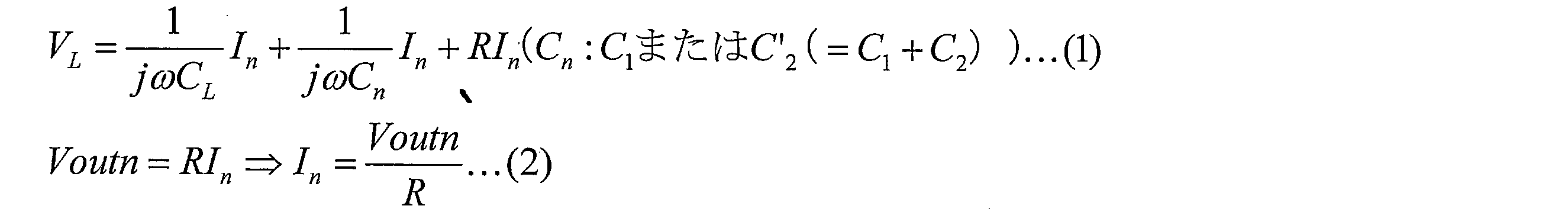
ここで、電気回路ECが第1の状態であるときに、導出部13に出力される電流をI1、出力電圧をVout1とし、電気回路ECが第2の状態であるときに、導出部13に出力される電流をI2、出力電圧をVout2とした。また、コンデンサC2の容量値は、コンデンサC1の容量値よりも十分大きい(C1<<C2)とした。
式(2)を式(1)に代入すると、
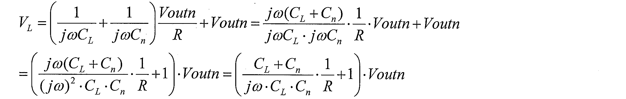
ゆえに、


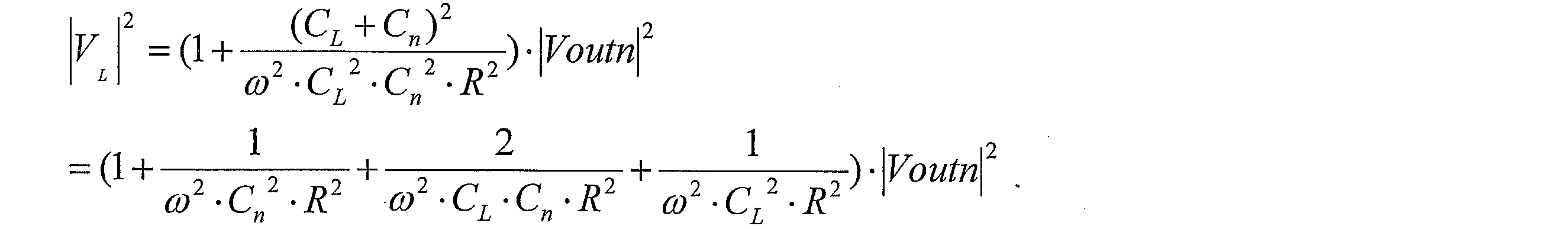
ゆえに、

従って、

図9に、計測対象電圧VLの絶対値の2回微分d|VL|2/dCLと、結合容量CLとの関係をグラフに示す。同図に示すグラフから、結合容量CLの容量値が大きいほど、d|VL|2/dCLの変動が小さいことが分かる。このことから、結合容量CLの容量値が大きいほど、計測対象電圧VLの計測値の変動および誤差が小さいことが、理論的に導かれる。
本発明は上述した各実施形態に限定されるものではなく、請求項に示した範囲で種々の変更が可能であり、異なる実施形態にそれぞれ開示された技術的手段を適宜組み合わせて得られる実施形態についても本発明の技術的範囲に含まれる。
〔まとめ〕
以上のように、本発明の一態様に係る非接触電圧計測装置は、プローブを備え、該プローブの電極と導体との間に結合容量が発生するように、該プローブを上記導体に非接触で近接させたとき、該プローブを介して電気回路に入力される電圧信号に基づいて、上記導体に印加される計測対象電圧を計測する非接触電圧計測装置において、上記電気回路の少なくとも一部を被覆することにより、上記電気回路に入射する電界を遮断する電界シールドを備え、上記プローブは、上記導体の形状に応じて変形し、かつ、上記電極と上記電界シールドとの間に発生する寄生容量の容量値を一定に維持する。
以上のように、本発明の一態様に係る非接触電圧計測装置は、プローブを備え、該プローブの電極と導体との間に結合容量が発生するように、該プローブを上記導体に非接触で近接させたとき、該プローブを介して電気回路に入力される電圧信号に基づいて、上記導体に印加される計測対象電圧を計測する非接触電圧計測装置において、上記電気回路の少なくとも一部を被覆することにより、上記電気回路に入射する電界を遮断する電界シールドを備え、上記プローブは、上記導体の形状に応じて変形し、かつ、上記電極と上記電界シールドとの間に発生する寄生容量の容量値を一定に維持する。
上記の構成によれば、プローブが備えた電極は、変形することが可能である。具体的には、電極は、導線(導体)の外線被覆に密着するように、変形することが可能であってよい。また、プローブは、電極が変形した場合であっても、電極と電界シールドとの間に発生する寄生容量の容量値を一定に維持する。
一般的に、プローブの電極と電界シールドとの間に発生する寄生容量が計測対象電圧の計測精度に与える影響は、キャリブレーションによって排除される。しかしながら、従来の構成では、電極の変形の度合いが変化することによって、電極と電界シールドとの間の距離も変化し、その結果、電極と電界シールドとの間に発生する寄生容量の容量値も変化する。そのため、従来の構成では、電極の変形の度合いによって、計測対象電圧の計測精度が変化するという問題があった。
一方、上記の構成によれば、プローブの変形の度合いが変化した場合であっても、電極と電界シールドとの間に発生する寄生容量の容量値は変化しない。
ゆえに、径の太さが異なる様々な導線の計測対象電圧を一定の精度で計測することができる。
本発明の他の態様に係る非接触電圧計測装置では、上記プローブは、上記導体の形状に応じて変形することが可能な第1電極と、上記電界シールドに対する相対的な位置を保持する第2電極と、を備えており、上記第1電極と上記第2電極とは、電気的に接続されており、上記第2電極は、上記第1電極と上記電界シールドとの間に発生する電界を遮蔽することが可能な位置に配置されていてもよい。
上記の構成によれば、プローブの第2電極は、電界シールドに対する相対的な位置を保持する。プローブの第1電極は、導体の形状に応じて変形する。
第1電極が変形した場合であっても、第2電極と電界シールドとの間の距離は変化しない。そのため、第2電極と電界シールドとの間に発生する寄生容量の容量値も変化しない。従って、第1電極がどれほど変形したとしても、第2電極と電界シールドとの間に発生する寄生容量を流れる漏れ電流の量は変化しない。
よって、第2電極と電界シールドとの間に発生する寄生容量を流れる漏れ電流の総量は、第1電極の変形の度合いによらず一定である。
さらに、上記の構成によれば、第2電極が、第1電極と電界シールドとの間に発生する電界を遮蔽可能な位置に配置されている。そのため、第1電極と電界シールドとの間に発生する寄生容量には漏れ電流が流れないので、プローブと電界シールドとの間を流れる漏れ電流の総量が減少し、計測対象電圧の計測精度が向上する。
また、上記の構成において、非接触電圧計測装置は、第1電極から電界シールドまでの距離よりも、第2電極から電界シールドまでの距離のほうが近くなるように構成されていてもよい。
この構成では、第1電極と電界シールドとの間に発生する寄生容量の容量値は、第2電極と電界シールドとの間に発生する寄生容量の容量値と比較して小さくなる。そのため、プローブと電界シールドとの間に発生する寄生容量の容量値全体に占める、第1電極と電界シールドとの間に発生する寄生容量の容量値の割合が小さくなる。従って、第1電極と電界シールドとの間に発生する寄生容量の値が変化したとき、その変化が計測対象電圧の計測精度に与える影響を抑制することができる。
本発明の他の態様に係る非接触電圧計測装置では、上記プローブは、上記導体の形状に応じて変形することが可能な変形部を備えており、上記変形部は、連結部によって互いに連結され、上記連結部を支点に回動する複数のアームで構成されており、複数の上記アームのうち少なくとも1つには、上記電極および上記電界シールドが、一定の距離で離間して配置されていてもよい。
上記の構成によれば、電極および電界シールドが、導体の形状に応じて変形する変形部が備えたアームに配置されている。変形部が変形するとき、変形部のアームは移動する。電極と電界シールドとは、同じアームに、一定の距離で離間して配置されているので、電極は、アームが移動したとき、電界シールドに対する相対的な位置を維持することができる。
従って、アームがどれほど移動したとしても、電極と電界シールドとの間に発生する寄生容量を流れる漏れ電流の量は変化しない。ゆえに、アームの移動量によらず、計測対象電圧を一定の精度で計測することができる。
本発明は、絶縁被覆された配線内の導線を流れる交流の電圧を、導線に接触することなく計測する電圧計測装置に利用することができる。
w 配線(導体)
EC 電気回路
VL 計測対象電圧
1 非接触電圧計測装置
11 検出プローブ(プローブ)
21 検出プローブ(プローブ)
211 電極
11A 内側電極(第1電極)
11B 外側電極(第2電極)
12 電界シールド
212 電界シールド
250 クランプ部(変形部)
250A 第1アーム(アーム)
250B 第2アーム(アーム)
260 連結部
EC 電気回路
VL 計測対象電圧
1 非接触電圧計測装置
11 検出プローブ(プローブ)
21 検出プローブ(プローブ)
211 電極
11A 内側電極(第1電極)
11B 外側電極(第2電極)
12 電界シールド
212 電界シールド
250 クランプ部(変形部)
250A 第1アーム(アーム)
250B 第2アーム(アーム)
260 連結部
Claims (3)
- プローブを備え、該プローブと導体との間に結合容量が発生するように、該プローブを上記導体に非接触で近接させたとき、該プローブを介して電気回路に入力される電圧信号に基づいて、上記導体に印加される計測対象電圧を計測する非接触電圧計測装置において、
上記電気回路の少なくとも一部を被覆することにより、上記電気回路に入射する電界を遮断する電界シールドを備え、
上記プローブは、上記導体の形状に応じて変形または移動する電極を備え、かつ、上記電極と上記電界シールドとの間に発生する寄生容量の容量値を一定に維持する
ことを特徴とする非接触電圧計測装置。 - 上記プローブは、
上記導体の形状に応じて変形することが可能な第1電極と、
上記電界シールドに対する相対的な位置を保持する第2電極と、
を備えており、
上記第1電極と上記第2電極とは、電気的に接続されており、
上記第2電極は、上記第1電極と上記電界シールドとの間に発生する電界を遮蔽することが可能な位置に配置されている
ことを特徴とする請求項1に記載の非接触電圧計測装置。 - 上記プローブは、
上記導体の形状に応じて変形することが可能な変形部を備えており、
上記変形部は、連結部によって互いに連結され、上記連結部を支点に回動する複数のアームで構成されており、
複数の上記アームのうち少なくとも1つには、上記電極および上記電界シールドが、一定の距離で離間して配置されている
ことを特徴とする請求項1に記載の非接触電圧計測装置。
Priority Applications (3)
| Application Number | Priority Date | Filing Date | Title |
|---|---|---|---|
| CN201580011383.5A CN106062569B (zh) | 2014-03-13 | 2015-02-04 | 非接触电压计测装置 |
| EP15760753.2A EP3118632B1 (en) | 2014-03-13 | 2015-02-04 | Non-contact voltage measurement device |
| US15/122,545 US10145865B2 (en) | 2014-03-13 | 2015-02-04 | Non-contact voltage measurement device |
Applications Claiming Priority (2)
| Application Number | Priority Date | Filing Date | Title |
|---|---|---|---|
| JP2014-050654 | 2014-03-13 | ||
| JP2014050654A JP6459188B2 (ja) | 2014-03-13 | 2014-03-13 | 非接触電圧計測装置 |
Publications (1)
| Publication Number | Publication Date |
|---|---|
| WO2015137017A1 true WO2015137017A1 (ja) | 2015-09-17 |
Family
ID=54071469
Family Applications (1)
| Application Number | Title | Priority Date | Filing Date |
|---|---|---|---|
| PCT/JP2015/053148 Ceased WO2015137017A1 (ja) | 2014-03-13 | 2015-02-04 | 非接触電圧計測装置 |
Country Status (5)
| Country | Link |
|---|---|
| US (1) | US10145865B2 (ja) |
| EP (1) | EP3118632B1 (ja) |
| JP (1) | JP6459188B2 (ja) |
| CN (1) | CN106062569B (ja) |
| WO (1) | WO2015137017A1 (ja) |
Families Citing this family (13)
| Publication number | Priority date | Publication date | Assignee | Title |
|---|---|---|---|---|
| US9786154B1 (en) | 2014-07-21 | 2017-10-10 | State Farm Mutual Automobile Insurance Company | Methods of facilitating emergency assistance |
| IT201600103234A1 (it) | 2016-10-14 | 2018-04-14 | Green Seas Ventures Ldt | Sistema Costruttivo afferente un sensore capacitivo di tensione |
| US11193958B2 (en) * | 2017-03-03 | 2021-12-07 | Veris Industries, Llc | Non-contact voltage sensor |
| US10120021B1 (en) * | 2017-06-16 | 2018-11-06 | Fluke Corporation | Thermal non-contact voltage and non-contact current devices |
| JP6989346B2 (ja) * | 2017-10-26 | 2022-01-05 | 大崎電気工業株式会社 | 電圧測定装置 |
| IT201800004114A1 (it) | 2018-03-30 | 2019-09-30 | Green Seas Ventures Ltd C/O Citco B V I Ltd | Sistema costruttivo afferente un sensore capacitivo di tensione |
| US10557875B2 (en) * | 2018-05-09 | 2020-02-11 | Fluke Corporation | Multi-sensor scanner configuration for non-contact voltage measurement devices |
| CN119986166A (zh) | 2018-12-17 | 2025-05-13 | G&W电气公司 | 电传感器组合件 |
| US11340266B2 (en) | 2018-12-17 | 2022-05-24 | G & W Electric Company | Electrical sensor assembly |
| JP2022062379A (ja) | 2020-10-08 | 2022-04-20 | ダイキン工業株式会社 | 電圧検出プローブおよび電極装着具 |
| CN113176441B (zh) * | 2021-06-11 | 2022-07-01 | 广西电网有限责任公司电力科学研究院 | 非接触电压测量装置、方法 |
| US11821925B2 (en) * | 2021-11-08 | 2023-11-21 | Fluke Corporation | Accessory for utilization with non-contact electrical detector |
| JP2023114811A (ja) * | 2022-02-07 | 2023-08-18 | オムロン株式会社 | クランプセンサ |
Citations (3)
| Publication number | Priority date | Publication date | Assignee | Title |
|---|---|---|---|---|
| JP2005214689A (ja) * | 2004-01-28 | 2005-08-11 | Yokogawa Electric Corp | 非接触電圧測定装置 |
| JP2006030141A (ja) * | 2004-07-21 | 2006-02-02 | Hioki Ee Corp | 静電誘導検出器のための電圧センサおよびクリップ |
| JP2012163394A (ja) * | 2011-02-04 | 2012-08-30 | Hitachi Electric Systems Ltd | 非接触電圧検出装置 |
Family Cites Families (15)
| Publication number | Priority date | Publication date | Assignee | Title |
|---|---|---|---|---|
| US3182257A (en) * | 1961-05-18 | 1965-05-04 | Motorola Inc | Electronic test probe |
| US3621392A (en) * | 1970-01-22 | 1971-11-16 | Thermal Ind Of Florida Inc | Connectionless electrical meter for measuring voltage or power factor |
| DE2313478C3 (de) * | 1973-03-15 | 1982-11-11 | Siemens AG, 1000 Berlin und 8000 München | Spannungswandler für eine mehrere Leiter führende, vollisolierte Hochspannungsschaltanlage |
| JPS5329928Y2 (ja) * | 1973-11-10 | 1978-07-26 | ||
| US4090130A (en) * | 1976-12-06 | 1978-05-16 | United Technologies Corporation | Capacitive coupled clamp-on voltage probe |
| JPS5833694Y2 (ja) * | 1978-09-26 | 1983-07-28 | 日新電機株式会社 | 密閉母線用電圧変成器 |
| JPS6319274U (ja) * | 1986-07-22 | 1988-02-08 | ||
| US5512838A (en) * | 1992-09-03 | 1996-04-30 | Hewlett-Packard Company | Probe with reduced input capacitance |
| US5473244A (en) * | 1992-09-17 | 1995-12-05 | Libove; Joel M. | Apparatus for measuring voltages and currents using non-contacting sensors |
| US6882158B2 (en) | 2001-01-24 | 2005-04-19 | General Dynamics Ots (Aerospace) Inc. | Series arc fault diagnostic for aircraft wiring |
| US7902854B2 (en) * | 2003-07-25 | 2011-03-08 | Power Measurement, Ltd. | Body capacitance electric field powered device for high voltage lines |
| JP2005127784A (ja) * | 2003-10-22 | 2005-05-19 | Yokogawa Electric Corp | 非接触電圧測定装置 |
| JP4995663B2 (ja) | 2007-08-06 | 2012-08-08 | 日置電機株式会社 | クランプ式センサ |
| JP4889689B2 (ja) * | 2008-06-30 | 2012-03-07 | 日本電信電話株式会社 | 非接触型電圧電流プローブ装置とこれを用いた電圧電流測定方法 |
| JP4995993B2 (ja) * | 2012-03-05 | 2012-08-08 | 日置電機株式会社 | クランプ式センサ |
-
2014
- 2014-03-13 JP JP2014050654A patent/JP6459188B2/ja not_active Expired - Fee Related
-
2015
- 2015-02-04 EP EP15760753.2A patent/EP3118632B1/en active Active
- 2015-02-04 US US15/122,545 patent/US10145865B2/en active Active
- 2015-02-04 CN CN201580011383.5A patent/CN106062569B/zh active Active
- 2015-02-04 WO PCT/JP2015/053148 patent/WO2015137017A1/ja not_active Ceased
Patent Citations (3)
| Publication number | Priority date | Publication date | Assignee | Title |
|---|---|---|---|---|
| JP2005214689A (ja) * | 2004-01-28 | 2005-08-11 | Yokogawa Electric Corp | 非接触電圧測定装置 |
| JP2006030141A (ja) * | 2004-07-21 | 2006-02-02 | Hioki Ee Corp | 静電誘導検出器のための電圧センサおよびクリップ |
| JP2012163394A (ja) * | 2011-02-04 | 2012-08-30 | Hitachi Electric Systems Ltd | 非接触電圧検出装置 |
Also Published As
| Publication number | Publication date |
|---|---|
| CN106062569A (zh) | 2016-10-26 |
| JP2015175654A (ja) | 2015-10-05 |
| EP3118632A1 (en) | 2017-01-18 |
| EP3118632A4 (en) | 2017-11-08 |
| US20170067939A1 (en) | 2017-03-09 |
| CN106062569B (zh) | 2019-02-15 |
| EP3118632B1 (en) | 2020-07-08 |
| JP6459188B2 (ja) | 2019-01-30 |
| US10145865B2 (en) | 2018-12-04 |
Similar Documents
| Publication | Publication Date | Title |
|---|---|---|
| JP6459188B2 (ja) | 非接触電圧計測装置 | |
| JP7182510B2 (ja) | 振動センサを有する非接触dc電圧測定装置 | |
| TWI742188B (zh) | 非接觸電壓測量系統 | |
| TWI744409B (zh) | 使用參考信號的非接觸式電壓測量系統 | |
| WO2015083618A1 (ja) | 非接触電圧測定装置および非接触電圧測定方法 | |
| CN107533091B (zh) | 非接触电压测量装置 | |
| JP5847339B1 (ja) | 非接触型交流電圧測定装置 | |
| JP5888421B2 (ja) | 交流電力測定装置及び交流電力測定方法 | |
| WO2015137018A1 (ja) | 非接触電圧計測装置 | |
| JPWO2017168608A1 (ja) | 非接触電圧測定装置および非接触電圧測定方法 | |
| JP6349748B2 (ja) | 非接触電圧計測装置 | |
| CN103582821B (zh) | 用于无接触确定对象的电位的装置、测电钳以及方法 | |
| JP2014044102A (ja) | 四端子抵抗測定装置、検査装置、四端子抵抗測定方法および検査方法 | |
| JP6054100B2 (ja) | 電力測定装置および電力測定方法 | |
| WO2015133212A1 (ja) | 電圧測定装置および電圧測定方法 | |
| JP6135777B2 (ja) | 材料試験機 | |
| JP2019078677A (ja) | 電圧測定装置 | |
| JP5615463B1 (ja) | 電圧検出装置および電圧検出方法 | |
| JP2005127784A (ja) | 非接触電圧測定装置 | |
| JP5963486B2 (ja) | 静電容量センサ、測定装置、および測定方法 | |
| JP6625422B2 (ja) | 測定装置 | |
| WO2021215390A1 (ja) | 静電容量型近接検出装置 | |
| JP2018159672A (ja) | 歪み検出装置及び歪み検出方法 |
Legal Events
| Date | Code | Title | Description |
|---|---|---|---|
| 121 | Ep: the epo has been informed by wipo that ep was designated in this application |
Ref document number: 15760753 Country of ref document: EP Kind code of ref document: A1 |
|
| WWE | Wipo information: entry into national phase |
Ref document number: 15122545 Country of ref document: US |
|
| REEP | Request for entry into the european phase |
Ref document number: 2015760753 Country of ref document: EP |
|
| WWE | Wipo information: entry into national phase |
Ref document number: 2015760753 Country of ref document: EP |
|
| NENP | Non-entry into the national phase |
Ref country code: DE |