WO2015141156A1 - ウエハ加工体、ウエハ加工用仮接着材、及び薄型ウエハの製造方法 - Google Patents
ウエハ加工体、ウエハ加工用仮接着材、及び薄型ウエハの製造方法 Download PDFInfo
- Publication number
- WO2015141156A1 WO2015141156A1 PCT/JP2015/001099 JP2015001099W WO2015141156A1 WO 2015141156 A1 WO2015141156 A1 WO 2015141156A1 JP 2015001099 W JP2015001099 W JP 2015001099W WO 2015141156 A1 WO2015141156 A1 WO 2015141156A1
- Authority
- WO
- WIPO (PCT)
- Prior art keywords
- wafer
- layer
- temporary adhesive
- polymer layer
- thermosetting siloxane
- Prior art date
- Legal status (The legal status is an assumption and is not a legal conclusion. Google has not performed a legal analysis and makes no representation as to the accuracy of the status listed.)
- Ceased
Links
- MJZXCGSHDGBPEP-UHFFFAOYSA-N C(C1OC1)OC1=C[I]=CC=C1 Chemical compound C(C1OC1)OC1=C[I]=CC=C1 MJZXCGSHDGBPEP-UHFFFAOYSA-N 0.000 description 2
- XEUJSBZUUZFTKZ-UHFFFAOYSA-N OC1=C[I]=CC=C1 Chemical compound OC1=C[I]=CC=C1 XEUJSBZUUZFTKZ-UHFFFAOYSA-N 0.000 description 2
- ISWSIDIOOBJBQZ-UHFFFAOYSA-N Oc1ccccc1 Chemical compound Oc1ccccc1 ISWSIDIOOBJBQZ-UHFFFAOYSA-N 0.000 description 2
Images
Classifications
-
- H—ELECTRICITY
- H10—SEMICONDUCTOR DEVICES; ELECTRIC SOLID-STATE DEVICES NOT OTHERWISE PROVIDED FOR
- H10P—GENERIC PROCESSES OR APPARATUS FOR THE MANUFACTURE OR TREATMENT OF DEVICES COVERED BY CLASS H10
- H10P72/00—Handling or holding of wafers, substrates or devices during manufacture or treatment thereof
- H10P72/70—Handling or holding of wafers, substrates or devices during manufacture or treatment thereof for supporting or gripping
- H10P72/74—Handling or holding of wafers, substrates or devices during manufacture or treatment thereof for supporting or gripping using temporarily an auxiliary support
- H10P72/7402—Wafer tapes, e.g. grinding or dicing support tapes
-
- B—PERFORMING OPERATIONS; TRANSPORTING
- B32—LAYERED PRODUCTS
- B32B—LAYERED PRODUCTS, i.e. PRODUCTS BUILT-UP OF STRATA OF FLAT OR NON-FLAT, e.g. CELLULAR OR HONEYCOMB, FORM
- B32B27/00—Layered products comprising a layer of synthetic resin
- B32B27/06—Layered products comprising a layer of synthetic resin as the main or only constituent of a layer, which is next to another layer of the same or of a different material
- B32B27/08—Layered products comprising a layer of synthetic resin as the main or only constituent of a layer, which is next to another layer of the same or of a different material of synthetic resin
-
- B—PERFORMING OPERATIONS; TRANSPORTING
- B32—LAYERED PRODUCTS
- B32B—LAYERED PRODUCTS, i.e. PRODUCTS BUILT-UP OF STRATA OF FLAT OR NON-FLAT, e.g. CELLULAR OR HONEYCOMB, FORM
- B32B27/00—Layered products comprising a layer of synthetic resin
- B32B27/18—Layered products comprising a layer of synthetic resin characterised by the use of special additives
- B32B27/26—Layered products comprising a layer of synthetic resin characterised by the use of special additives using curing agents
-
- B—PERFORMING OPERATIONS; TRANSPORTING
- B32—LAYERED PRODUCTS
- B32B—LAYERED PRODUCTS, i.e. PRODUCTS BUILT-UP OF STRATA OF FLAT OR NON-FLAT, e.g. CELLULAR OR HONEYCOMB, FORM
- B32B27/00—Layered products comprising a layer of synthetic resin
- B32B27/28—Layered products comprising a layer of synthetic resin comprising synthetic resins not wholly covered by any one of the sub-groups B32B27/30 - B32B27/42
- B32B27/283—Layered products comprising a layer of synthetic resin comprising synthetic resins not wholly covered by any one of the sub-groups B32B27/30 - B32B27/42 comprising polysiloxanes
-
- B—PERFORMING OPERATIONS; TRANSPORTING
- B32—LAYERED PRODUCTS
- B32B—LAYERED PRODUCTS, i.e. PRODUCTS BUILT-UP OF STRATA OF FLAT OR NON-FLAT, e.g. CELLULAR OR HONEYCOMB, FORM
- B32B37/00—Methods or apparatus for laminating, e.g. by curing or by ultrasonic bonding
- B32B37/12—Methods or apparatus for laminating, e.g. by curing or by ultrasonic bonding characterised by using adhesives
-
- B—PERFORMING OPERATIONS; TRANSPORTING
- B32—LAYERED PRODUCTS
- B32B—LAYERED PRODUCTS, i.e. PRODUCTS BUILT-UP OF STRATA OF FLAT OR NON-FLAT, e.g. CELLULAR OR HONEYCOMB, FORM
- B32B7/00—Layered products characterised by the relation between layers; Layered products characterised by the relative orientation of features between layers, or by the relative values of a measurable parameter between layers, i.e. products comprising layers having different physical, chemical or physicochemical properties; Layered products characterised by the interconnection of layers
- B32B7/04—Interconnection of layers
- B32B7/06—Interconnection of layers permitting easy separation
-
- B—PERFORMING OPERATIONS; TRANSPORTING
- B32—LAYERED PRODUCTS
- B32B—LAYERED PRODUCTS, i.e. PRODUCTS BUILT-UP OF STRATA OF FLAT OR NON-FLAT, e.g. CELLULAR OR HONEYCOMB, FORM
- B32B7/00—Layered products characterised by the relation between layers; Layered products characterised by the relative orientation of features between layers, or by the relative values of a measurable parameter between layers, i.e. products comprising layers having different physical, chemical or physicochemical properties; Layered products characterised by the interconnection of layers
- B32B7/04—Interconnection of layers
- B32B7/12—Interconnection of layers using interposed adhesives or interposed materials with bonding properties
-
- C—CHEMISTRY; METALLURGY
- C08—ORGANIC MACROMOLECULAR COMPOUNDS; THEIR PREPARATION OR CHEMICAL WORKING-UP; COMPOSITIONS BASED THEREON
- C08G—MACROMOLECULAR COMPOUNDS OBTAINED OTHERWISE THAN BY REACTIONS ONLY INVOLVING UNSATURATED CARBON-TO-CARBON BONDS
- C08G77/00—Macromolecular compounds obtained by reactions forming a linkage containing silicon with or without sulfur, nitrogen, oxygen or carbon in the main chain of the macromolecule
- C08G77/04—Polysiloxanes
- C08G77/20—Polysiloxanes containing silicon bound to unsaturated aliphatic groups
-
- C—CHEMISTRY; METALLURGY
- C08—ORGANIC MACROMOLECULAR COMPOUNDS; THEIR PREPARATION OR CHEMICAL WORKING-UP; COMPOSITIONS BASED THEREON
- C08K—Use of inorganic or non-macromolecular organic substances as compounding ingredients
- C08K5/00—Use of organic ingredients
- C08K5/56—Organo-metallic compounds, i.e. organic compounds containing a metal-to-carbon bond
-
- C—CHEMISTRY; METALLURGY
- C08—ORGANIC MACROMOLECULAR COMPOUNDS; THEIR PREPARATION OR CHEMICAL WORKING-UP; COMPOSITIONS BASED THEREON
- C08L—COMPOSITIONS OF MACROMOLECULAR COMPOUNDS
- C08L83/00—Compositions of macromolecular compounds obtained by reactions forming in the main chain of the macromolecule a linkage containing silicon with or without sulfur, nitrogen, oxygen or carbon only; Compositions of derivatives of such polymers
-
- C—CHEMISTRY; METALLURGY
- C09—DYES; PAINTS; POLISHES; NATURAL RESINS; ADHESIVES; COMPOSITIONS NOT OTHERWISE PROVIDED FOR; APPLICATIONS OF MATERIALS NOT OTHERWISE PROVIDED FOR
- C09J—ADHESIVES; NON-MECHANICAL ASPECTS OF ADHESIVE PROCESSES IN GENERAL; ADHESIVE PROCESSES NOT PROVIDED FOR ELSEWHERE; USE OF MATERIALS AS ADHESIVES
- C09J11/00—Features of adhesives not provided for in group C09J9/00, e.g. additives
- C09J11/02—Non-macromolecular additives
- C09J11/04—Non-macromolecular additives inorganic
-
- C—CHEMISTRY; METALLURGY
- C09—DYES; PAINTS; POLISHES; NATURAL RESINS; ADHESIVES; COMPOSITIONS NOT OTHERWISE PROVIDED FOR; APPLICATIONS OF MATERIALS NOT OTHERWISE PROVIDED FOR
- C09J—ADHESIVES; NON-MECHANICAL ASPECTS OF ADHESIVE PROCESSES IN GENERAL; ADHESIVE PROCESSES NOT PROVIDED FOR ELSEWHERE; USE OF MATERIALS AS ADHESIVES
- C09J11/00—Features of adhesives not provided for in group C09J9/00, e.g. additives
- C09J11/02—Non-macromolecular additives
- C09J11/06—Non-macromolecular additives organic
-
- C—CHEMISTRY; METALLURGY
- C09—DYES; PAINTS; POLISHES; NATURAL RESINS; ADHESIVES; COMPOSITIONS NOT OTHERWISE PROVIDED FOR; APPLICATIONS OF MATERIALS NOT OTHERWISE PROVIDED FOR
- C09J—ADHESIVES; NON-MECHANICAL ASPECTS OF ADHESIVE PROCESSES IN GENERAL; ADHESIVE PROCESSES NOT PROVIDED FOR ELSEWHERE; USE OF MATERIALS AS ADHESIVES
- C09J183/00—Adhesives based on macromolecular compounds obtained by reactions forming in the main chain of the macromolecule a linkage containing silicon, with or without sulfur, nitrogen, oxygen, or carbon only; Adhesives based on derivatives of such polymers
- C09J183/04—Polysiloxanes
-
- C—CHEMISTRY; METALLURGY
- C09—DYES; PAINTS; POLISHES; NATURAL RESINS; ADHESIVES; COMPOSITIONS NOT OTHERWISE PROVIDED FOR; APPLICATIONS OF MATERIALS NOT OTHERWISE PROVIDED FOR
- C09J—ADHESIVES; NON-MECHANICAL ASPECTS OF ADHESIVE PROCESSES IN GENERAL; ADHESIVE PROCESSES NOT PROVIDED FOR ELSEWHERE; USE OF MATERIALS AS ADHESIVES
- C09J201/00—Adhesives based on unspecified macromolecular compounds
-
- C—CHEMISTRY; METALLURGY
- C09—DYES; PAINTS; POLISHES; NATURAL RESINS; ADHESIVES; COMPOSITIONS NOT OTHERWISE PROVIDED FOR; APPLICATIONS OF MATERIALS NOT OTHERWISE PROVIDED FOR
- C09J—ADHESIVES; NON-MECHANICAL ASPECTS OF ADHESIVE PROCESSES IN GENERAL; ADHESIVE PROCESSES NOT PROVIDED FOR ELSEWHERE; USE OF MATERIALS AS ADHESIVES
- C09J7/00—Adhesives in the form of films or foils
- C09J7/10—Adhesives in the form of films or foils without carriers
-
- C—CHEMISTRY; METALLURGY
- C09—DYES; PAINTS; POLISHES; NATURAL RESINS; ADHESIVES; COMPOSITIONS NOT OTHERWISE PROVIDED FOR; APPLICATIONS OF MATERIALS NOT OTHERWISE PROVIDED FOR
- C09J—ADHESIVES; NON-MECHANICAL ASPECTS OF ADHESIVE PROCESSES IN GENERAL; ADHESIVE PROCESSES NOT PROVIDED FOR ELSEWHERE; USE OF MATERIALS AS ADHESIVES
- C09J7/00—Adhesives in the form of films or foils
- C09J7/20—Adhesives in the form of films or foils characterised by their carriers
- C09J7/201—Adhesives in the form of films or foils characterised by their carriers characterised by the release coating composition on the carrier layer
-
- C—CHEMISTRY; METALLURGY
- C09—DYES; PAINTS; POLISHES; NATURAL RESINS; ADHESIVES; COMPOSITIONS NOT OTHERWISE PROVIDED FOR; APPLICATIONS OF MATERIALS NOT OTHERWISE PROVIDED FOR
- C09J—ADHESIVES; NON-MECHANICAL ASPECTS OF ADHESIVE PROCESSES IN GENERAL; ADHESIVE PROCESSES NOT PROVIDED FOR ELSEWHERE; USE OF MATERIALS AS ADHESIVES
- C09J7/00—Adhesives in the form of films or foils
- C09J7/20—Adhesives in the form of films or foils characterised by their carriers
- C09J7/203—Adhesives in the form of films or foils characterised by their carriers characterised by the structure of the release feature on the carrier layer
-
- C—CHEMISTRY; METALLURGY
- C09—DYES; PAINTS; POLISHES; NATURAL RESINS; ADHESIVES; COMPOSITIONS NOT OTHERWISE PROVIDED FOR; APPLICATIONS OF MATERIALS NOT OTHERWISE PROVIDED FOR
- C09J—ADHESIVES; NON-MECHANICAL ASPECTS OF ADHESIVE PROCESSES IN GENERAL; ADHESIVE PROCESSES NOT PROVIDED FOR ELSEWHERE; USE OF MATERIALS AS ADHESIVES
- C09J7/00—Adhesives in the form of films or foils
- C09J7/30—Adhesives in the form of films or foils characterised by the adhesive composition
-
- C—CHEMISTRY; METALLURGY
- C09—DYES; PAINTS; POLISHES; NATURAL RESINS; ADHESIVES; COMPOSITIONS NOT OTHERWISE PROVIDED FOR; APPLICATIONS OF MATERIALS NOT OTHERWISE PROVIDED FOR
- C09J—ADHESIVES; NON-MECHANICAL ASPECTS OF ADHESIVE PROCESSES IN GENERAL; ADHESIVE PROCESSES NOT PROVIDED FOR ELSEWHERE; USE OF MATERIALS AS ADHESIVES
- C09J7/00—Adhesives in the form of films or foils
- C09J7/40—Adhesives in the form of films or foils characterised by release liners
- C09J7/401—Adhesives in the form of films or foils characterised by release liners characterised by the release coating composition
-
- C—CHEMISTRY; METALLURGY
- C09—DYES; PAINTS; POLISHES; NATURAL RESINS; ADHESIVES; COMPOSITIONS NOT OTHERWISE PROVIDED FOR; APPLICATIONS OF MATERIALS NOT OTHERWISE PROVIDED FOR
- C09J—ADHESIVES; NON-MECHANICAL ASPECTS OF ADHESIVE PROCESSES IN GENERAL; ADHESIVE PROCESSES NOT PROVIDED FOR ELSEWHERE; USE OF MATERIALS AS ADHESIVES
- C09J7/00—Adhesives in the form of films or foils
- C09J7/40—Adhesives in the form of films or foils characterised by release liners
- C09J7/403—Adhesives in the form of films or foils characterised by release liners characterised by the structure of the release feature
-
- C—CHEMISTRY; METALLURGY
- C09—DYES; PAINTS; POLISHES; NATURAL RESINS; ADHESIVES; COMPOSITIONS NOT OTHERWISE PROVIDED FOR; APPLICATIONS OF MATERIALS NOT OTHERWISE PROVIDED FOR
- C09J—ADHESIVES; NON-MECHANICAL ASPECTS OF ADHESIVE PROCESSES IN GENERAL; ADHESIVE PROCESSES NOT PROVIDED FOR ELSEWHERE; USE OF MATERIALS AS ADHESIVES
- C09J7/00—Adhesives in the form of films or foils
- C09J7/50—Adhesives in the form of films or foils characterised by a primer layer between the carrier and the adhesive
-
- H—ELECTRICITY
- H10—SEMICONDUCTOR DEVICES; ELECTRIC SOLID-STATE DEVICES NOT OTHERWISE PROVIDED FOR
- H10P—GENERIC PROCESSES OR APPARATUS FOR THE MANUFACTURE OR TREATMENT OF DEVICES COVERED BY CLASS H10
- H10P72/00—Handling or holding of wafers, substrates or devices during manufacture or treatment thereof
- H10P72/70—Handling or holding of wafers, substrates or devices during manufacture or treatment thereof for supporting or gripping
- H10P72/74—Handling or holding of wafers, substrates or devices during manufacture or treatment thereof for supporting or gripping using temporarily an auxiliary support
- H10P72/7448—Handling or holding of wafers, substrates or devices during manufacture or treatment thereof for supporting or gripping using temporarily an auxiliary support the bond interface between the auxiliary support and the wafer comprising two or more, e.g. multilayer adhesive or adhesive and release layer
- H10P72/745—Handling or holding of wafers, substrates or devices during manufacture or treatment thereof for supporting or gripping using temporarily an auxiliary support the bond interface between the auxiliary support and the wafer comprising two or more, e.g. multilayer adhesive or adhesive and release layer the bond interface between the auxiliary support and the wafer comprises three or more layers
-
- B—PERFORMING OPERATIONS; TRANSPORTING
- B32—LAYERED PRODUCTS
- B32B—LAYERED PRODUCTS, i.e. PRODUCTS BUILT-UP OF STRATA OF FLAT OR NON-FLAT, e.g. CELLULAR OR HONEYCOMB, FORM
- B32B37/00—Methods or apparatus for laminating, e.g. by curing or by ultrasonic bonding
- B32B37/12—Methods or apparatus for laminating, e.g. by curing or by ultrasonic bonding characterised by using adhesives
- B32B2037/1269—Methods or apparatus for laminating, e.g. by curing or by ultrasonic bonding characterised by using adhesives multi-component adhesive
-
- B—PERFORMING OPERATIONS; TRANSPORTING
- B32—LAYERED PRODUCTS
- B32B—LAYERED PRODUCTS, i.e. PRODUCTS BUILT-UP OF STRATA OF FLAT OR NON-FLAT, e.g. CELLULAR OR HONEYCOMB, FORM
- B32B2250/00—Layers arrangement
- B32B2250/03—3 layers
-
- B—PERFORMING OPERATIONS; TRANSPORTING
- B32—LAYERED PRODUCTS
- B32B—LAYERED PRODUCTS, i.e. PRODUCTS BUILT-UP OF STRATA OF FLAT OR NON-FLAT, e.g. CELLULAR OR HONEYCOMB, FORM
- B32B2264/00—Composition or properties of particles which form a particulate layer or are present as additives
-
- B—PERFORMING OPERATIONS; TRANSPORTING
- B32—LAYERED PRODUCTS
- B32B—LAYERED PRODUCTS, i.e. PRODUCTS BUILT-UP OF STRATA OF FLAT OR NON-FLAT, e.g. CELLULAR OR HONEYCOMB, FORM
- B32B2264/00—Composition or properties of particles which form a particulate layer or are present as additives
- B32B2264/02—Synthetic macromolecular particles
-
- B—PERFORMING OPERATIONS; TRANSPORTING
- B32—LAYERED PRODUCTS
- B32B—LAYERED PRODUCTS, i.e. PRODUCTS BUILT-UP OF STRATA OF FLAT OR NON-FLAT, e.g. CELLULAR OR HONEYCOMB, FORM
- B32B2307/00—Properties of the layers or laminate
- B32B2307/70—Other properties
- B32B2307/732—Dimensional properties
-
- B—PERFORMING OPERATIONS; TRANSPORTING
- B32—LAYERED PRODUCTS
- B32B—LAYERED PRODUCTS, i.e. PRODUCTS BUILT-UP OF STRATA OF FLAT OR NON-FLAT, e.g. CELLULAR OR HONEYCOMB, FORM
- B32B2307/00—Properties of the layers or laminate
- B32B2307/70—Other properties
- B32B2307/748—Releasability
-
- B—PERFORMING OPERATIONS; TRANSPORTING
- B32—LAYERED PRODUCTS
- B32B—LAYERED PRODUCTS, i.e. PRODUCTS BUILT-UP OF STRATA OF FLAT OR NON-FLAT, e.g. CELLULAR OR HONEYCOMB, FORM
- B32B2405/00—Adhesive articles, e.g. adhesive tapes
-
- B—PERFORMING OPERATIONS; TRANSPORTING
- B32—LAYERED PRODUCTS
- B32B—LAYERED PRODUCTS, i.e. PRODUCTS BUILT-UP OF STRATA OF FLAT OR NON-FLAT, e.g. CELLULAR OR HONEYCOMB, FORM
- B32B2457/00—Electrical equipment
- B32B2457/08—PCBs, i.e. printed circuit boards
-
- B—PERFORMING OPERATIONS; TRANSPORTING
- B32—LAYERED PRODUCTS
- B32B—LAYERED PRODUCTS, i.e. PRODUCTS BUILT-UP OF STRATA OF FLAT OR NON-FLAT, e.g. CELLULAR OR HONEYCOMB, FORM
- B32B2457/00—Electrical equipment
- B32B2457/14—Semiconductor wafers
-
- C—CHEMISTRY; METALLURGY
- C08—ORGANIC MACROMOLECULAR COMPOUNDS; THEIR PREPARATION OR CHEMICAL WORKING-UP; COMPOSITIONS BASED THEREON
- C08G—MACROMOLECULAR COMPOUNDS OBTAINED OTHERWISE THAN BY REACTIONS ONLY INVOLVING UNSATURATED CARBON-TO-CARBON BONDS
- C08G77/00—Macromolecular compounds obtained by reactions forming a linkage containing silicon with or without sulfur, nitrogen, oxygen or carbon in the main chain of the macromolecule
- C08G77/04—Polysiloxanes
- C08G77/12—Polysiloxanes containing silicon bound to hydrogen
-
- C—CHEMISTRY; METALLURGY
- C09—DYES; PAINTS; POLISHES; NATURAL RESINS; ADHESIVES; COMPOSITIONS NOT OTHERWISE PROVIDED FOR; APPLICATIONS OF MATERIALS NOT OTHERWISE PROVIDED FOR
- C09J—ADHESIVES; NON-MECHANICAL ASPECTS OF ADHESIVE PROCESSES IN GENERAL; ADHESIVE PROCESSES NOT PROVIDED FOR ELSEWHERE; USE OF MATERIALS AS ADHESIVES
- C09J2203/00—Applications of adhesives in processes or use of adhesives in the form of films or foils
- C09J2203/326—Applications of adhesives in processes or use of adhesives in the form of films or foils for bonding electronic components such as wafers, chips or semiconductors
-
- C—CHEMISTRY; METALLURGY
- C09—DYES; PAINTS; POLISHES; NATURAL RESINS; ADHESIVES; COMPOSITIONS NOT OTHERWISE PROVIDED FOR; APPLICATIONS OF MATERIALS NOT OTHERWISE PROVIDED FOR
- C09J—ADHESIVES; NON-MECHANICAL ASPECTS OF ADHESIVE PROCESSES IN GENERAL; ADHESIVE PROCESSES NOT PROVIDED FOR ELSEWHERE; USE OF MATERIALS AS ADHESIVES
- C09J2301/00—Additional features of adhesives in the form of films or foils
- C09J2301/20—Additional features of adhesives in the form of films or foils characterized by the structural features of the adhesive itself
- C09J2301/208—Additional features of adhesives in the form of films or foils characterized by the structural features of the adhesive itself the adhesive layer being constituted by at least two or more adjacent or superposed adhesive layers, e.g. multilayer adhesive
-
- C—CHEMISTRY; METALLURGY
- C09—DYES; PAINTS; POLISHES; NATURAL RESINS; ADHESIVES; COMPOSITIONS NOT OTHERWISE PROVIDED FOR; APPLICATIONS OF MATERIALS NOT OTHERWISE PROVIDED FOR
- C09J—ADHESIVES; NON-MECHANICAL ASPECTS OF ADHESIVE PROCESSES IN GENERAL; ADHESIVE PROCESSES NOT PROVIDED FOR ELSEWHERE; USE OF MATERIALS AS ADHESIVES
- C09J2301/00—Additional features of adhesives in the form of films or foils
- C09J2301/30—Additional features of adhesives in the form of films or foils characterized by the chemical, physicochemical or physical properties of the adhesive or the carrier
- C09J2301/304—Additional features of adhesives in the form of films or foils characterized by the chemical, physicochemical or physical properties of the adhesive or the carrier the adhesive being heat-activatable, i.e. not tacky at temperatures inferior to 30°C
-
- C—CHEMISTRY; METALLURGY
- C09—DYES; PAINTS; POLISHES; NATURAL RESINS; ADHESIVES; COMPOSITIONS NOT OTHERWISE PROVIDED FOR; APPLICATIONS OF MATERIALS NOT OTHERWISE PROVIDED FOR
- C09J—ADHESIVES; NON-MECHANICAL ASPECTS OF ADHESIVE PROCESSES IN GENERAL; ADHESIVE PROCESSES NOT PROVIDED FOR ELSEWHERE; USE OF MATERIALS AS ADHESIVES
- C09J2483/00—Presence of polysiloxane
-
- H—ELECTRICITY
- H10—SEMICONDUCTOR DEVICES; ELECTRIC SOLID-STATE DEVICES NOT OTHERWISE PROVIDED FOR
- H10P—GENERIC PROCESSES OR APPARATUS FOR THE MANUFACTURE OR TREATMENT OF DEVICES COVERED BY CLASS H10
- H10P72/00—Handling or holding of wafers, substrates or devices during manufacture or treatment thereof
- H10P72/70—Handling or holding of wafers, substrates or devices during manufacture or treatment thereof for supporting or gripping
- H10P72/74—Handling or holding of wafers, substrates or devices during manufacture or treatment thereof for supporting or gripping using temporarily an auxiliary support
- H10P72/7416—Handling or holding of wafers, substrates or devices during manufacture or treatment thereof for supporting or gripping using temporarily an auxiliary support used during dicing or grinding
-
- H—ELECTRICITY
- H10—SEMICONDUCTOR DEVICES; ELECTRIC SOLID-STATE DEVICES NOT OTHERWISE PROVIDED FOR
- H10P—GENERIC PROCESSES OR APPARATUS FOR THE MANUFACTURE OR TREATMENT OF DEVICES COVERED BY CLASS H10
- H10P72/00—Handling or holding of wafers, substrates or devices during manufacture or treatment thereof
- H10P72/70—Handling or holding of wafers, substrates or devices during manufacture or treatment thereof for supporting or gripping
- H10P72/74—Handling or holding of wafers, substrates or devices during manufacture or treatment thereof for supporting or gripping using temporarily an auxiliary support
- H10P72/7422—Handling or holding of wafers, substrates or devices during manufacture or treatment thereof for supporting or gripping using temporarily an auxiliary support used to protect an active side of a device or wafer
-
- H—ELECTRICITY
- H10—SEMICONDUCTOR DEVICES; ELECTRIC SOLID-STATE DEVICES NOT OTHERWISE PROVIDED FOR
- H10P—GENERIC PROCESSES OR APPARATUS FOR THE MANUFACTURE OR TREATMENT OF DEVICES COVERED BY CLASS H10
- H10P72/00—Handling or holding of wafers, substrates or devices during manufacture or treatment thereof
- H10P72/70—Handling or holding of wafers, substrates or devices during manufacture or treatment thereof for supporting or gripping
- H10P72/74—Handling or holding of wafers, substrates or devices during manufacture or treatment thereof for supporting or gripping using temporarily an auxiliary support
- H10P72/744—Details of chemical or physical process used for separating the auxiliary support from a device or a wafer
- H10P72/7442—Separation by peeling
-
- H—ELECTRICITY
- H10—SEMICONDUCTOR DEVICES; ELECTRIC SOLID-STATE DEVICES NOT OTHERWISE PROVIDED FOR
- H10W—GENERIC PACKAGES, INTERCONNECTIONS, CONNECTORS OR OTHER CONSTRUCTIONAL DETAILS OF DEVICES COVERED BY CLASS H10
- H10W72/00—Interconnections or connectors in packages
- H10W72/20—Bump connectors, e.g. solder bumps or copper pillars; Dummy bumps; Thermal bumps
- H10W72/251—Materials
- H10W72/252—Materials comprising solid metals or solid metalloids, e.g. PbSn, Ag or Cu
Definitions
- the present invention relates to a wafer processed body, a temporary adhesive for wafer processing, and a method for manufacturing a thin wafer, which make it possible to effectively obtain a thin wafer.
- the three-dimensional mounting technology is a semiconductor manufacturing technology in which one semiconductor chip is thinned and further laminated in multiple layers while being connected by a through silicon via (TSV).
- TSV through silicon via
- a back surface protective tape has been applied to the opposite side of the ground surface to prevent wafer damage during grinding.
- this tape uses an organic resin film as a supporting substrate, and is flexible, but has insufficient strength and heat resistance, and is not suitable for performing a TSV forming process or a wiring layer forming process on the back surface. .
- Patent Document 1 a technique for peeling an adhesive layer from a support by irradiating an adhesive containing a light-absorbing substance with high-intensity light and decomposing the adhesive layer.
- Patent Document 2 a technique that uses a heat-meltable hydrocarbon-based compound as an adhesive and performs bonding and peeling in a heat-melted state has been proposed.
- the former technique requires an expensive apparatus such as a laser, and has a problem that the processing time per substrate becomes long.
- the latter technique is simple because it is controlled only by heating, but its application range is narrow because the thermal stability at a high temperature exceeding 200 ° C. is insufficient.
- these temporary adhesive layers are not suitable for forming a uniform film thickness of a high step substrate and for complete adhesion to a support.
- Patent Document 3 a technique using a silicone adhesive for the temporary adhesive layer has been proposed.
- the substrate is bonded to the support using an addition-curing silicone adhesive, and the substrate is separated from the support by immersing in a chemical that dissolves or decomposes the silicone resin at the time of peeling. . Therefore, it takes a very long time for peeling, and application to an actual manufacturing process is difficult.
- the present invention has been made in view of the above-described problems, and can be easily bonded temporarily, and can be formed with a uniform film thickness on a high step substrate, and is compatible with TSV formation and wafer backside wiring processes.
- it has excellent wafer thermal process resistance such as CVD (Chemical Vapor Deposition), is easy to peel off, and can improve the productivity of thin wafers, temporary adhesive for wafer processing, and the same
- An object of the present invention is to provide a method for manufacturing a thin wafer using CVD (Chemical Vapor Deposition), is easy to peel off, and can improve the productivity of thin wafers, temporary adhesive for wafer processing, and the same
- An object of the present invention is to provide a method for manufacturing a thin wafer using CVD (Chemical Vapor Deposition), is easy to peel off, and can improve the productivity of thin wafers, temporary adhesive for wafer processing, and the same
- An object of the present invention is to provide a method for manufacturing a thin wafer using CVD (
- a wafer processing temporary adhesive for temporarily bonding a wafer having a circuit surface on a front surface and a back surface to be processed to a support, From a first temporary adhesive layer comprising a non-silicone thermoplastic resin layer (A) that can be peelably adhered to the surface of the wafer, and a thermosetting siloxane polymer layer (B) laminated on the first temporary adhesive layer.
- a three-layer structure comprising a second temporary adhesive layer and a third temporary adhesive layer laminated on the second temporary adhesive layer and comprising a thermosetting siloxane-modified polymer layer (C) that can be peelably adhered to the support.
- a temporary adhesive for wafer processing comprising a composite temporary adhesive material layer having
- the present invention is a wafer processed body in which a temporary adhesive layer is formed on a support, and a wafer having a circuit surface on the front surface and a back surface processed is laminated on the temporary adhesive layer.
- a first temporary adhesive layer comprising a non-silicone thermoplastic resin layer (A), wherein the temporary adhesive layer is releasably bonded to the surface of the wafer; and a thermosetting siloxane laminated on the first temporary adhesive layer.
- a second temporary adhesive layer composed of a polymer layer (B), and a third temporary layer composed of a thermosetting siloxane-modified polymer layer (C) laminated on the second temporary adhesive layer and peelably adhered to the support.
- a wafer processed body comprising a composite temporary adhesive material layer having a three-layer structure with a temporary adhesive layer.
- thermosetting siloxane polymer layer (B) is (B-1) an organopolysiloxane having two or more alkenyl groups in one molecule; (B-2) Organohydrogenpolysiloxane containing hydrogen atoms (Si—H groups) bonded to two or more silicon atoms in one molecule: (B— 2) An amount in which the molar ratio of Si—H groups in the component is from 0.3 to 10, (B-3) platinum-based catalyst, It is preferable that it is a hardened
- thermosetting siloxane polymer layer (B) is preferable because it is superior in CVD resistance.
- thermosetting siloxane polymer layer (B) is further added to a total of 100 parts by mass of the reaction control agent (B-1) and the component (B-2) as the component (B-4). 0.1 to 10 parts by mass, It is preferable that it contains.
- thermosetting siloxane polymer layer (B) can prevent the treatment liquid (composition) from being thickened or gelled before heat curing.
- the 180 ° peel strength of the 25 mm wide test piece after the thermosetting of the thermosetting siloxane polymer layer (B) is 2 gf or more and 50 gf or less.
- thermosetting siloxane polymer layer (B) having such a peel-peeling force is preferable because there is no risk of wafer misalignment during wafer grinding, and peeling is easy.
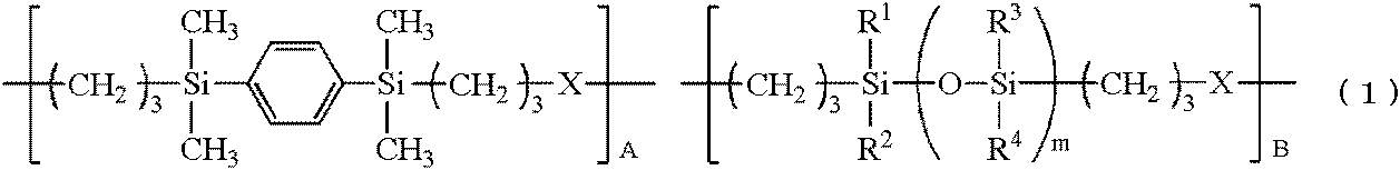
- thermosetting siloxane-modified polymer layer (C) has a weight average molecular weight having a repeating unit represented by the following general formula (1) of 3,000 to 500,000, preferably 10,000 to 100,000.
- R 1 to R 4 represent a monovalent hydrocarbon group having 1 to 8 carbon atoms which may be the same or different.
- M is an integer from 1 to 100
- B is a positive number
- A is 0 or a positive number.
- a + B 1.
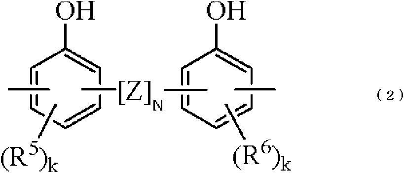
- X is a divalent organic group represented by the following general formula (2). (Where Z is A divalent organic group selected from any one of the following: N is 0 or 1; R 5 and R 6 are each an alkyl group or alkoxy group having 1 to 4 carbon atoms, and may be the same or different from each other. k is 0, 1, or 2. ]]
- thermosetting siloxane-modified polymer layer (C) is preferable because it is more excellent in heat resistance.
- thermosetting siloxane-modified polymer layer (C) has a repeating unit represented by the following general formula (3) and has a weight average molecular weight of 3,000 to 500,000 and a siloxane bond-containing polymer 100.
- a cured product layer of a composition containing 0.1 to 50 parts by mass of one or more types is preferable.
- R 1 to R 4 represent a monovalent hydrocarbon group having 1 to 8 carbon atoms which may be the same or different.
- M is an integer from 1 to 100
- B is a positive number
- A is 0 or a positive number.
- a + B 1.
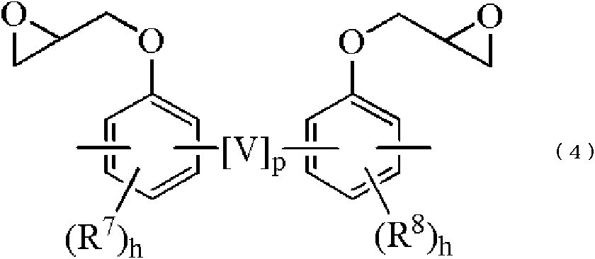
- Y is a divalent organic group represented by the following general formula (4). (Where V is And a p is 0 or 1.
- R 7 and R 8 are each an alkyl group or alkoxy group having 1 to 4 carbon atoms, and may be the same or different from each other. h is 0, 1, or 2. ]]
- thermosetting siloxane-modified polymer layer (C) is preferable because it is more excellent in heat resistance.
- thermoplastic resin layer used for the temporary adhesive for wafer processing of the present invention wherein the circuit forming surface of the wafer having a circuit forming surface on the front surface and a circuit non-forming surface on the back surface is used.
- thermosetting siloxane polymer layer (B) When joining to a support via a temporary adhesive layer composed of (A), the thermosetting siloxane polymer layer (B), and the thermosetting siloxane-modified polymer layer (C), After forming the thermosetting siloxane polymer layer (B) on the thermosetting siloxane-modified polymer layer (C) formed on the support, the polymer layers (C) and (B) Bonding the formed support and the wafer with a circuit formed with the resin layer (A) under vacuum; (B) thermosetting the polymer layers (B) and (C); (C) grinding or polishing a non-circuit-formed surface of the wafer bonded to the support; (D) processing the non-circuit-formed surface of the wafer; (E) a step of peeling the processed wafer from the support; A method for manufacturing a thin wafer is provided.
- the temporary adhesive layer composed of the three-layer system according to the present invention is used for bonding the wafer and the support, and the through-electrode structure is formed using the temporary adhesive layer.
- a thin wafer having a bump connection structure can be easily manufactured.
- the temporary adhesive layer in the present invention has a three-layer structure, and in particular, by using a thermosetting siloxane-modified resin (polymer layer (C)) as a substrate bonding support layer, thermal decomposition of the resin does not occur.
- a thermosetting siloxane-modified resin polymer layer (C)
- the resin flow does not occur especially at a high temperature of 200 ° C. or higher, and the heat resistance is high, so that it can be applied to a wide range of semiconductor film forming processes, and the film thickness uniformity can be applied to a wafer having a step. It is possible to form a high adhesive layer, and it is possible to easily obtain a uniform thin wafer having a thickness of 50 ⁇ m or less because of the uniformity of the film thickness.
- thermosetting siloxane polymer layer (B) as a polymer layer (B), it is excellent by CVD tolerance.
- thermoplastic temporary adhesive layer comprising a non-silicone thermoplastic resin layer
- thermosetting temporary adhesive layer comprising a thermosetting siloxane polymer layer
- a composite temporary adhesive layer composed of a three-layer system composed of a thermosetting temporary adhesive layer composed of a thermosetting siloxane-modified polymer layer of (C) is bonded to the wafer and the support from the wafer side (A), (B ) And (C) were used as a structure formed in this order, and a method for easily manufacturing a thin wafer having a through electrode structure and a bump connection structure was found.
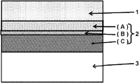
- FIG. 1 is a cross-sectional view showing an example of a wafer processed body of the present invention.
- a wafer processed body of the present invention has a circuit surface on the front surface, a wafer (device wafer) 1 to be processed on the back surface, and a support 3 that supports the wafer 1 when processing the wafer 1.
- Siloxane polymer layer (B) second temporary adhesive layer
- further a thermosetting siloxane-modified polymer layer (C) third temporary adhesive layer).
- the surface of the wafer 1 is releasably bonded, and the third temporary adhesive layer is removably bonded to the support 3.
- the temporary adhesive for wafer processing according to the present invention is composed of the laminates (A), (B) and (C).
- thermoplastic resin layer (thermoplastic organopolysiloxane-free polymer layer)-
- the first temporary adhesive layer (A) is composed of a thermoplastic resin having no organopolysiloxane. Due to its applicability to silicon wafers having a level difference, a thermoplastic resin having good spin coatability is suitably used as a material for forming the first temporary adhesive layer (A), and in particular, has a glass transition temperature of ⁇ 80 to 120 ° C.
- thermoplastic resin of a certain degree is preferable, and examples thereof include olefin-based thermoplastic elastomers, polybutadiene-based thermoplastic elastomers, styrene-based thermoplastic elastomers, styrene-butadiene-based thermoplastic elastomers, styrene-polyolefin-based thermoplastic elastomers, etc.
- a hydrogenated polystyrene elastomer excellent in the above is suitable. Specific examples include Tuftec (Asahi Kasei Chemicals), Espolex SB series (Sumitomo Chemical), Lavalon (Mitsubishi Chemical), Septon (Kuraray), and DYNARON (JSR).
- cycloolefin polymer represented by ZEONEX Nippon ZEON
- TOPAS Nippon Polyplastics
- the non-silicone thermoplastic resin layer (A) is preferably a non-silicone thermoplastic elastomer.
- the wafer after the thin wafer is manufactured, the wafer can be easily peeled off from the support, so that the thin wafer which is easily broken can be handled more easily.
- This non-silicone thermoplastic resin layer is dissolved in a solvent and formed on a semiconductor substrate such as a silicon wafer by a method such as spin coating or spray coating.
- the solvent include hydrocarbon solvents, preferably nonane, p-menthane, pinene, isooctane, and the like. Nonane, p-menthane, and isooctane are more preferable because of their coating properties.
- the film thickness to be formed is not limited, but it is desirable to form a resin film according to the step on the substrate, preferably 0.5 to 50 microns, more preferably 0.5 to A film thickness of 10 ⁇ m is formed.
- an antioxidant and a surfactant can be added to the thermoplastic resin for improving the coating property.
- the antioxidant di-t-butylphenol is preferably used.
- the surfactant a fluorosilicone surfactant X-70-1102 (manufactured by Shin-Etsu Chemical Co., Ltd.) and the like are preferably used.
- thermosetting siloxane polymer layer (B) that is a constituent element of the wafer processed body and the wafer processing temporary adhesive of the present invention is not particularly limited as long as it is made of a thermosetting siloxane polymer.
- a cured product layer of a composition containing the following components (B-1) to (B-3) and, if necessary, the component (B-4) is preferable.
- (B-1) an organopolysiloxane having two or more alkenyl groups in one molecule;
- B-2 Organohydrogenpolysiloxane containing hydrogen atoms (Si—H groups) bonded to two or more silicon atoms in one molecule: (B-2) with respect to alkenyl groups in component (B-1) )
- An amount such that the molar ratio of Si—H groups in the component is 0.3 to 10, (B-3) Platinum-based catalyst.
- thermosetting siloxane polymer layer (B) is further added to the reaction control agent (B-1) and the component (B-2) as a component (B-4) in an amount of 0.1 parts by weight. It is preferable that it contains 1 to 10 parts by mass.
- Component (B-1) is an organopolysiloxane having two or more alkenyl groups in one molecule.
- the component (B-1) is preferably a linear or branched diorganopolysiloxane containing two or more alkenyl groups in one molecule.
- Particularly preferred are diorganopolysiloxanes containing 0.3 to 10 mol%, especially 0.6 mol% (number of moles of alkenyl groups / number of moles of Si) to 9 mol% in one molecule.
- R 9 (3-a) X a SiO- (R 9 XSiO) m - (R 9 2 SiO) n -SiR 9 (3-a) X a ... (5)
- R 9 is independently a monovalent hydrocarbon group having no aliphatic unsaturated bond
- X is independently an alkenyl group-containing monovalent organic group
- a is an integer of 0 to 3.
- 2a + m is a number at which the alkenyl group content is 0.3 to 10 mol% in one molecule
- m + 2 is an alkenyl group content of 0.1 in one molecule.
- the number is 3 to 10 mol%.
- M is a positive number of 0 or 10 or less
- n is a positive number of 1 to 1000.
- R 9 is preferably a monovalent hydrocarbon group having 1 to 10 carbon atoms.
- an alkyl group such as a methyl group, an ethyl group, a propyl group, or a butyl group
- a cycloalkyl group such as a cyclohexyl group
- An aryl group such as a phenyl group and a tolyl group, and an alkyl group such as a methyl group or a phenyl group is particularly preferable.
- the alkenyl group-containing monovalent organic group represented by X is preferably an organic group having 2 to 10 carbon atoms, and an alkenyl group such as a vinyl group, an allyl group, a hexenyl group, or an octenyl group; an acryloylpropyl group, an acryloylmethyl group, or a methacryloylpropyl group.
- (Meth) acryloylalkyl groups such as groups; (meth) acryloxyalkyl groups such as acryloxypropyl groups, acryloxymethyl groups, methacryloxypropyl groups, methacryloxymethyl groups; cyclohexenylethyl groups, vinyloxypropyl groups, etc.
- An alkenyl group-containing monovalent hydrocarbon group is exemplified, and a vinyl group is particularly preferred industrially.
- the properties of the alkenyl group-containing diorganopolysiloxane are preferably oily or raw rubbery.
- the alkenyl group-containing diorganopolysiloxane may be linear or branched.
- Component (B-2) is a crosslinking agent, and is an organohydrogenpolysiloxane containing hydrogen atoms (Si—H groups) bonded to two or more silicon atoms in one molecule.
- the component (B-2) has at least 2, preferably 3 or more hydrogen atoms (SiH groups) bonded to a silicon atom in one molecule, and is linear, branched, or cyclic. Can be used.
- the viscosity of the organohydrogenpolysiloxane (B-2) at 25 ° C. is preferably 1 to 5,000 mPa ⁇ s, and more preferably 5 to 500 mPa ⁇ s.
- the organohydrogenpolysiloxane may be a mixture of two or more.
- the molar ratio of the Si—H group in the component (B-2) to the alkenyl group in the component (B-1) (SiH group / alkenyl group) is 0.3 to 10, particularly 1 It is preferable to blend in the range of 0.0 to 8.0. If the molar ratio between the SiH group and the alkenyl group is 0.3 or more, the crosslinking density does not decrease and the problem that the pressure-sensitive adhesive layer does not cure does not occur. If it is 10 or less, the crosslinking density does not become too high, and sufficient adhesive force and tack can be obtained. Moreover, if said molar ratio is 10 or less, the usable time of a process liquid can be lengthened.
- Component (B-3) is a platinum-based catalyst (that is, a platinum group metal catalyst) such as chloroplatinic acid, an alcohol solution of chloroplatinic acid, a reaction product of chloroplatinic acid and alcohol, chloroplatinic acid and an olefin compound. And a reaction product of chloroplatinic acid and a vinyl group-containing siloxane.
- a platinum-based catalyst that is, a platinum group metal catalyst
- the amount of component (B-3) added is an effective amount, and is generally the sum of (B-1) and (B-2) (when component (B-4) shown below is contained, (B-1 ), (B-2) and (B-4)), the platinum content (in terms of mass) is 1 to 5,000 ppm, preferably 5 to 2,000 ppm. If it is 1 ppm or more, the curability of the composition does not decrease, the crosslinking density does not decrease, and the holding power does not decrease. If it is 0.5% or less, the usable time of the treatment bath can be lengthened.
- Component (B-4) is a reaction control agent, and is used as necessary to prevent the treatment liquid from thickening or gelling before heat curing when the composition is prepared or applied to the substrate. Can be optionally added.
- Specific examples include 3-methyl-1-butyn-3-ol, 3-methyl-1-pentyn-3-ol, 3,5-dimethyl-1-hexyn-3-ol, 1-ethynylcyclohexanol, 3 -Methyl-3-trimethylsiloxy-1-butyne, 3-methyl-3-trimethylsiloxy-1-pentyne, 3,5-dimethyl-3-trimethylsiloxy-1-hexyne, 1-ethynyl-1-trimethylsiloxycyclohexane, Bis (2,2-dimethyl-3-butynoxy) dimethylsilane, 1,3,5,7-tetramethyl-1,3,5,7-tetravinylcyclotetrasiloxane, 1,1,3,3-tetramethyl 1,3-divinyldisiloxane and the like, and 1-ethynylcyclohexanol and 3-methyl-1-butyne-3-o are preferable. It is.
- the blending amount is 0.1 to 10 parts by mass with respect to 100 parts by mass in total of the components (B-1) and (B-2). Is preferred.
- the amount is more preferably 0.1 to 8.0 parts by mass, particularly preferably 0.1 to 2.0 parts by mass. If it is 10 parts by mass or less, the curability of the silicone pressure-sensitive adhesive composition does not decrease, and if it is 0.1 parts by mass or more, the effect of reaction control is sufficiently exhibited.
- thermosetting siloxane polymer layer (B) has R 10 3 SiO 0.5 units (wherein R 10 is independently an unsubstituted or substituted monovalent hydrocarbon group having 1 to 10 carbon atoms) and A polyorganosiloxane containing SiO 2 units and having a molar ratio of R 10 3 SiO 0.5 units / SiO 2 units of 0.3 to 1.8 may be added.
- the addition amount is preferably 0 to 30% by mass of the component (B-1) in the thermosetting siloxane polymer layer (B).
- thermosetting siloxane polymer layer (B) is formed on the uncured thermosetting siloxane-modified polymer layer (C) formed on the support by a method such as spin coating or roll coater. Can be used.
- a hydrocarbon solvent such as pentane, hexane, cyclohexane, isooctane, nonane, decane, p-menthane, pinene, isododecane and limonene is preferably used.
- a known antioxidant can be added to the solution of the polymer layer (B) in order to improve heat resistance.
- thermosetting siloxane polymer layer (B) is used by being formed with a film thickness of 0.1 to 30 ⁇ m, preferably 1.0 to 15 ⁇ m.
- the film thickness is 0.1 ⁇ m or more, it can be applied to the whole without producing a portion that cannot be applied when applied on the thermosetting siloxane-modified polymer layer (C).
- the film thickness is 30 ⁇ m or less, it can withstand the grinding process in forming a thin wafer.
- thermosetting siloxane polymer layer (B) may be added to the thermosetting siloxane polymer layer (B) in an amount of 50 parts by mass or less with respect to 100 parts by mass of the polymer layer (B). Good.
- thermosetting siloxane polymer layer (B) has a 180 ° peel strength of a 25 mm wide test piece (for example, a polyimide test piece) after thermosetting, usually 2 gf or more and 50 gf or less, preferably 3 gf. It is 30 gf or less, more preferably 5 gf or more and 20 gf or less. If it is 2 gf or more, there is no fear of wafer misalignment during wafer grinding, and if it is 50 gf or less, the wafer can be easily peeled off.
- a 25 mm wide test piece for example, a polyimide test piece
- thermosetting siloxane-modified polymer layer (C) which is a component of the wafer processed body and the wafer processing temporary adhesive according to the present invention, is not particularly limited as long as it is a thermosetting siloxane-modified polymer layer.
- a layer of a cured product of a thermosetting composition mainly comprising the thermosetting siloxane-modified polymer represented by (1) or (3) is preferable.
- Polymer of general formula (1) (phenolic siloxane polymer): A siloxane bond-containing polymer having a repeating unit represented by the following general formula (1) and having a weight average molecular weight of 3,000 to 500,000, preferably 10,000 to 100,000.
- R 1 to R 4 represent a monovalent hydrocarbon group having 1 to 8 carbon atoms which may be the same or different.
- M is an integer from 1 to 100
- B is a positive number
- A is 0 or a positive number.
- A is 0 to 0.9
- B is 0.1 to 1
- A is preferably 0.1 to 0.7
- B is 0.3 to 0.9. It is.
- Z is A divalent organic group selected from any one of the following: N is 0 or 1; R 5 and R 6 are each an alkyl group or alkoxy group having 1 to 4 carbon atoms, and may be the same or different from each other. k is 0, 1, or 2. ]]
- R 1 to R 4 include a methyl group, an ethyl group, a phenyl group, and the like, and m is preferably an integer of 3 to 60, more preferably 8 to 40.
- B / A is 0 to 20, particularly 0.5 to 5.
- Polymer of general formula (3) (epoxy-modified siloxane polymer): A siloxane bond-containing polymer having a repeating unit represented by the following general formula (3) and having a weight average molecular weight of 3,000 to 500,000.
- R 1 to R 4 represent a monovalent hydrocarbon group having 1 to 8 carbon atoms which may be the same or different.
- M is an integer from 1 to 100
- B is a positive number
- A is 0 or a positive number.
- A is 0 to 0.9
- B is 0.1 to 1
- A is preferably 0.1 to 0.7
- B is 0.3 to 0.9. It is.
- V is And a p is 0 or 1.
- R 7 and R 8 are each an alkyl group or alkoxy group having 1 to 4 carbon atoms, and may be the same or different from each other.
- h is 0, 1, or 2.
- thermosetting composition mainly composed of the thermosetting siloxane-modified polymer of the general formula (1) or (3) is used for the thermosetting.
- one or more crosslinking agents selected from epoxy compounds having two or more epoxy groups is used for the thermosetting.
- examples of the amino condensate, melamine resin, and urea resin modified with formalin or formalin-alcohol include the following.
- a melamine resin (condensate) modified with formalin or formalin-alcohol is a modified melamine monomer (for example, trimethoxymethylmonomethylolmelamine) or a multimer (for example, an oligomer such as a dimer or trimer).
- a melamine resin (condensate) modified with formalin or formalin-alcohol is a modified melamine monomer (for example, trimethoxymethylmonomethylolmelamine) or a multimer (for example, an oligomer such as a dimer or trimer).
- a modified melamine monomer for example, trimethoxymethylmonomethylolmelamine
- a multimer for example, an oligomer such as a dimer or trimer.
- these can be used 1 type or in mixture of 2 or more types.
- Preparation of a urea resin (condensate) modified with formalin or formalin-alcohol is, for example, modified by methylolation of a urea condensate of a desired molecular weight with formalin according to a known method, or further alkoxylated with alcohol. And may be denatured.
- Specific examples of the urea resin modified with formalin or formalin-alcohol include, for example, methoxymethylated urea condensate, ethoxymethylated urea condensate, propoxymethylated urea condensate and the like. In addition, these can be used 1 type or in mixture of 2 or more types.
- phenol compound having an average of two or more methylol groups or alkoxymethylol groups in one molecule examples include (2-hydroxy-5-methyl) -1,3-benzenedimethanol, 2,2 ′, Examples include 6,6′-tetramethoxymethylbisphenol A.
- these phenol compounds can be used 1 type or in mixture of 2 or more types.
- an epoxy compound having an average of two or more epoxy groups in one molecule or an average of two or more phenol groups in one molecule 1 type or more of the phenolic compound which has these is contained as a crosslinking agent.
- the epoxy compound having a polyfunctional epoxy group used in the general formulas (1) and (3) is not particularly limited, but in particular, a bifunctional, trifunctional, tetrafunctional or higher polyfunctional epoxy resin,
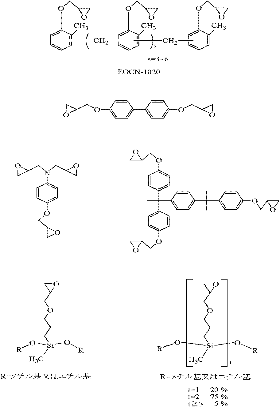
- a bifunctional, trifunctional, tetrafunctional or higher polyfunctional epoxy resin For example, EOCN-1020, EOCN-102S, XD-1000, NC-2000-L, EPPN-201, GAN, NC6000 manufactured by Nippon Kayaku Co., Ltd. or a crosslinking agent represented by the following formula can be contained.
- thermosetting siloxane-modified polymer is an epoxy-modified siloxane polymer of the above general formula (3)
- m p-based cresol novolak resin
- EP-6030G manufactured by Asahi Organic Materials Industries, Ltd.
- trifunctional phenolic compounds such as Tris-P-PA manufactured by Honshu Chemical Co., Ltd.
- tetrafunctional phenolic compounds such as TEP-TPA manufactured by Asahi Organic Materials Corporation.
- the amount of the crosslinking agent is 0.1 to 50 parts by weight, preferably 0.1 to 30 parts by weight, more preferably 1 to 20 parts by weight, based on 100 parts by weight of the thermosetting siloxane-modified polymer. You may mix and mix a kind or 3 or more types.
- thermosetting siloxane-modified polymer 10 parts by mass or less of a curing catalyst such as an acid anhydride may be added to 100 parts by mass of the thermosetting siloxane-modified polymer.
- this composition may be dissolved in a solution and formed on a support by coating, specifically by a method such as spin coating, roll coater or die coater.
- a method such as spin coating, roll coater or die coater.
- ketones such as cyclohexanone, cyclopentanone, methyl-2-n-amyl ketone; 3-methoxybutanol, 3-methyl-3-methoxybutanol, 1-methoxy-2-propanol, 1-ethoxy -Alcohols such as 2-propanol; ethers such as propylene glycol monomethyl ether, ethylene glycol monomethyl ether, propylene glycol monoethyl ether, ethylene glycol monoethyl ether, propylene glycol dimethyl ether, diethylene glycol dimethyl ether; propylene glycol monomethyl ether acetate, propylene glycol Monoethyl ether acetate, ethyl lactate, ethyl
- a filler such as a known antioxidant or silica may be added in an amount of 50 parts by mass or less based on 100 parts by mass of the thermosetting siloxane-modified polymer.
- a surfactant may be added to improve the coating uniformity.
- antioxidants that can be added to the polymer layer (C) include tetrakis [methylene- (3,5-di-t-butyl-4-hydroxyhydrocinnamate)] methane (trade name: Examples include hindered phenol compounds such as ADK STAB (AO-60).
- thermosetting siloxane-modified polymer layer (C) made of the above-mentioned thermosetting siloxane-modified polymer preferably has a film thickness upon curing of 15 to 150 ⁇ m, preferably 20 to 120 ⁇ m, depending on the level difference on the wafer side. It is more preferable to form a film with If the film thickness is 15 ⁇ m or more, it can sufficiently withstand the grinding process for thinning the wafer, and if it is 150 ⁇ m or less, there is no risk of resin deformation in the heat treatment process such as the TSV forming process, and it can withstand practical use. Therefore, it is preferable.
- the method for producing a thin wafer of the present invention comprises a non-silicone thermoplastic resin layer (A), a thermosetting siloxane polymer layer (B) and a thermosetting siloxane as an adhesive layer between a wafer having a semiconductor circuit and the support.
- a composite temporary adhesive layer including three layers of the modified polymer layer (C) is used.
- the thickness of the thin wafer obtained by the production method of the present invention is typically 5 to 300 ⁇ m, more typically 10 to 100 ⁇ m.
- the thin wafer manufacturing method of the present invention includes the steps (a) to (e). Further, steps (f) to (i) are included as necessary.
- Step (a) In the step (a), a circuit forming surface of a wafer having a circuit forming surface on the front surface and a circuit non-forming surface on the back surface is formed on the non-silicone thermoplastic resin layer (A) used for the wafer processing temporary adhesive material of the present invention. And formed on the support when bonded to the support through the temporary adhesive layer composed of the thermosetting siloxane polymer layer (B) and the thermosetting siloxane-modified polymer layer (C).
- thermosetting siloxane polymer layer (B) After forming the thermosetting siloxane polymer layer (B) on the thermosetting siloxane-modified polymer layer (C), the support on which the polymer layers (C) and (B) are formed, and the resin layer In this step, the wafer with circuit formed in (A) is bonded together under vacuum.
- a wafer having a circuit formation surface and a circuit non-formation surface is a wafer in which one surface is a circuit formation surface and the other surface is a circuit non-formation surface.
- a wafer to which the present invention is applicable is usually a semiconductor wafer.
- the semiconductor wafer include not only a silicon wafer but also a germanium wafer, a gallium-arsenic wafer, a gallium-phosphorus wafer, a gallium-arsenic-aluminum wafer, and the like.
- the thickness of the wafer is not particularly limited, but is typically 600 to 800 ⁇ m, more typically 625 to 775 ⁇ m.
- a substrate such as a silicon wafer, a glass plate, or a quartz wafer can be used as the support, but there is no limitation.
- the support it is not necessary to irradiate the temporary adhesive layer through the support with radiant energy rays, and the support may not have light transmittance.
- Each of the temporary adhesive layers (A), (B) and (C) is a film and can be formed on a wafer or a support, or each solution can be applied to the wafer or the support by a method such as spin coating or roll coater. Can be formed.
- pre-baking is performed in advance at a temperature of 80 to 200 ° C., preferably 100 to 180 ° C., depending on the volatilization conditions of the solvent, and then used.
- the temporary adhesion layer (A) layer, the wafer on which the (B) layer and the (C) layer are formed, and the support are formed as a bonded substrate through the (A), (B) and (C) layers.
- the At this time preferably in the temperature range of 40 to 200 ° C., more preferably 60 to 180 ° C., the wafer is bonded to the support by uniformly pressing the substrate under reduced pressure at this temperature ( Laminate substrate) is formed.
- Examples of the wafer bonding apparatus include commercially available wafer bonding apparatuses such as EVG520IS and 850TB manufactured by EVG, and XBC300 manufactured by SUSS.
- Step (b) is a step of thermally curing the polymer layers (B) and (C). After the processed wafer (laminated substrate) is formed, the polymer layer (B) is heated at 120 to 220 ° C., preferably 150 to 200 ° C. for 10 minutes to 4 hours, preferably 30 minutes to 2 hours. ) And (C) are cured.
- the step (c) is a step of grinding or polishing the non-circuit-formed surface of the wafer bonded to the support, that is, grinding the wafer back surface side of the wafer processed body obtained by bonding in the step (a), This is a step of reducing the thickness of the wafer.
- the grinding is preferably performed while cooling the wafer and a grindstone (such as diamond) with water.
- Examples of the apparatus for grinding the back surface of the wafer include DAG-810 (trade name) manufactured by DISCO Corporation. Further, the back side of the wafer may be subjected to CMP polishing.
- Step (d) is a step of processing the wafer non-circuited surface of the non-circuit-formed surface, that is, the non-circuit-formed surface of the wafer processed body thinned by back surface grinding.
- This process includes various processes used at the wafer level. Examples include electrode formation, metal wiring formation, protective film formation, and the like.
- metal sputtering for forming electrodes, etc. wet etching for etching a metal sputtering layer, application of a resist to form a mask for forming a metal wiring, pattern formation by exposure and development, resist peeling
- dry etching metal plating
- silicon etching for TSV formation and formation of an oxide film on the silicon surface can be mentioned.
- step (e) the wafer processed in step (d) is peeled off from the support, that is, after various processing is performed on the thinned wafer, the wafer is peeled off from the support before dicing. It is a process.
- This peeling process is generally performed under a relatively low temperature condition of room temperature to about 60 ° C., one of the wafer and the support of the wafer processed body is fixed horizontally, and the other is attached at a certain angle from the horizontal direction. Examples thereof include a method of lifting, a method of attaching a protective film to the ground surface of the ground wafer, and peeling the wafer and the protective film from the wafer processed body by a peel method.
- the present invention can be applied to any of these peeling methods.
- the method is not limited to the above method.
- These peeling methods are usually performed at room temperature.
- step (e) of peeling the processed wafer from the support (F) bonding a dicing tape to the wafer surface of the processed wafer; (G) a step of vacuum adsorbing the dicing tape surface to the adsorption surface; (H) It is preferable to include a step of peeling the support from the processed wafer by peel-off in a temperature range of 10 ° C. to 100 ° C. By doing in this way, a support body can be easily peeled from the processed wafer, and a subsequent dicing process can be performed easily.
- step (I) It is preferable to perform a step of removing the temporary adhesive layer remaining on the circuit forming surface of the peeled wafer.
- a part of the temporary adhesive layer (A) may remain on the circuit forming surface of the wafer peeled off from the support in the step (e).
- the temporary adhesive layer (A) may be removed by removing the temporary adhesive layer (A) from the wafer. Can be performed by washing.
- any cleaning solution that dissolves the non-silicone thermoplastic resin layer (A) in the temporary adhesive layer can be used.
- pentane, hexane examples include cyclohexane, decane, isononane, p-menthane, pinene, isododecane, and limonene.
- bases and acids may be added to the solvent. Examples of bases that can be used include amines such as ethanolamine, diethanolamine, triethanolamine, triethylamine, and ammonia, and ammonium salts such as tetramethylammonium hydroxide.
- the acids organic acids such as acetic acid, oxalic acid, benzenesulfonic acid, and dodecylbenzenesulfonic acid can be used.
- the addition amount is 0.01 to 10% by mass, preferably 0.1 to 5% by mass in terms of the concentration in the cleaning solution.
- an existing surfactant may be added.
- a cleaning method a method of performing cleaning with a paddle using the above liquid, a cleaning method of spraying, and a method of immersing in a cleaning liquid tank are possible.
- the temperature is preferably 10 to 80 ° C., preferably 15 to 65 ° C. If necessary, the layer (A) is dissolved with these solutions, and finally washed with water or rinsed with alcohol, followed by drying treatment. Thus, a thin wafer can be obtained.
- the mixture was further aged at 80 ° C. for 2 hours, and then toluene was distilled off and 80 g of cyclohexanone was added to obtain a resin solution containing cyclohexanone having a resin solid content concentration of 50% by mass as a solvent.
- the weight average molecular weight was 45,000 in terms of polystyrene.
- EOCN-1020 manufactured by Nippon Kayaku Co., Ltd.
- BSDM bis ( tert-butylsulfonyl) diazomethane
- tetrakis [methylene- (3,5-di-tert-butyl-4-hydroxyhydrocinnamate)] methane (trade name: ADK STAB AO-) as an antioxidant 60) was added and filtered through a 1 ⁇ m membrane filter to obtain a resin solution (C-1).
- TEP-TPA Asahi Organic Materials Co., Ltd.
- tetrahydrophthalic anhydride manufactured by Shin Nippon Rika Co., Ltd., Ricacid HH-A
- a solution composed of 80 parts by mass of polydimethylsiloxane having 0.5 mol% vinyl group in the molecular side chain and a number average molecular weight (Mn) of 30,000 and 400 parts by mass of isododecane is represented by the following formula (M-6). 3.0 parts of the organohydrogenpolysiloxane and 0.7 parts of ethynylcyclohexanol were added and mixed. Further, 0.5 part of platinum catalyst CAT-PL-5 (manufactured by Shin-Etsu Chemical Co., Ltd.) was added and filtered through a 0.2 ⁇ m membrane filter to obtain a thermosetting siloxane polymer solution (B-1). .
- thermosetting siloxane polymer solution (B-2).
- Resin Solution Preparation Example 4 An organo (M-6) represented by (M-6) in a solution comprising 80 parts by mass of polydimethylsiloxane having 400 mol parts of polydimethylsiloxane having 5 mol% vinyl groups at both ends and side chains and a number average molecular weight (Mn) of 30,000. 7.5 parts of hydrogen polysiloxane and 0.7 parts of ethynylcyclohexanol were added and mixed. Further, 0.5 part of platinum catalyst CAT-PL-5 (manufactured by Shin-Etsu Chemical Co., Ltd.) was added and filtered through a 0.2 ⁇ m membrane filter to obtain a thermosetting siloxane polymer solution (B-3). .
- Mn number average molecular weight
- Examples 1 to 3 and Comparative Example 1 After spin coating on a 200 mm diameter silicon wafer (thickness: 725 ⁇ m) with a copper post having a height of 10 ⁇ m and a diameter of 40 ⁇ m on the entire surface, the substrate is heated at 150 ° C. for 5 minutes on a hot plate. The material corresponding to the layer was formed on the wafer bump forming surface with the film thickness shown in Table 1. On the other hand, a glass plate having a diameter of 200 mm (thickness: 500 ⁇ m) is used as a support, and a polymer solution corresponding to the layer (C) is first heated on the support by spin coating and hot plate at 150 ° C. for 5 minutes.
- thermosetting siloxane polymer corresponding to the layer (B) was spin-coated on the layer (C) formed on the glass support, so that the film thicknesses shown in Table 1 were formed. . After that, it was heated on a hot plate at 150 ° C. for 3 minutes.
- the silicon wafer having the non-silicone thermoplastic resin layer (A), the (C) layer comprising the thermosetting siloxane-modified polymer layer, and the glass having the (B) layer on the (C) layer were bonded to each other under the conditions shown in Table 1 in a vacuum bonding apparatus so that the resin surfaces were aligned, to produce a processed wafer.
- a glass plate is used as a support in order to visually discriminate abnormalities after bonding the substrate, but a silicon substrate that does not transmit light, such as a wafer, can also be used.
- Plasma CVD PD270STL manufactured by Samco
- a dicing tape was applied to the wafer side thinned to 50 ⁇ m of the processed wafer after the CVD resistance test using a dicing frame, and this dicing tape surface was set on the suction plate by vacuum suction. . Thereafter, the glass substrate was peeled off by lifting one point of the glass with tweezers at room temperature. A case where the 50 ⁇ m wafer could be peeled without being broken was indicated by “ ⁇ ”, and a case where an abnormality such as a crack occurred was evaluated as defective and indicated by “X”.
- -Peel peel test After spin-coating on a silicon wafer with a diameter of 200 mm (thickness: 725 ⁇ m), it is heated on a hot plate at 150 ° C. for 5 minutes, so that the material corresponding to layer (A) has the film thickness shown in Table 1 and the wafer bump formation surface A film was formed. Thereafter, a solution of a thermosetting siloxane polymer corresponding to the layer (B) is also spin-coated on the layer (A) formed on the silicon wafer, and then further heated at 150 ° C. for 3 minutes on a hot plate. And was formed to a thickness of 2 ⁇ m.
- the polymer solution corresponding to the (C) layer was formed on the silicon wafer with a film thickness of 50 ⁇ m by heating the polymer solution corresponding to the (C) layer on the (B) layer by spin coating and hot plate at 150 ° C. for 5 minutes. Thereafter, it was cured in an oven at 180 ° C. for 1 hour. Thereafter, five polyimide tapes of 150 mm length ⁇ 25 mm width were affixed onto the (C) layer of the wafer, and the temporary adhesive layer where the tape was not stretched was removed. Using an AUTOGRAPH (AG-1) manufactured by Shimadzu Corporation, peel 120mm from one end of the tape by 180 ° peeling at a speed of 300mm / min. The average force (120mm stroke x 5 times) is shown in (B) The peel strength of the temporary adhesive layer was used.
- AG-1 AUTOGRAPH
- the present invention is not limited to the above embodiment.
- the above-described embodiment is an exemplification, and the present invention has any configuration that has substantially the same configuration as the technical idea described in the claims of the present invention and that exhibits the same effects. Are included in the technical scope.
Landscapes
- Chemical & Material Sciences (AREA)
- Organic Chemistry (AREA)
- Chemical Kinetics & Catalysis (AREA)
- Health & Medical Sciences (AREA)
- Medicinal Chemistry (AREA)
- Polymers & Plastics (AREA)
- Inorganic Chemistry (AREA)
- Adhesives Or Adhesive Processes (AREA)
- Mechanical Treatment Of Semiconductor (AREA)
- Laminated Bodies (AREA)
- Container, Conveyance, Adherence, Positioning, Of Wafer (AREA)
- Compositions Of Macromolecular Compounds (AREA)
Abstract
Description
前記ウエハの表面に剥離可能に接着可能な非シリコーン熱可塑性樹脂層(A)からなる第一仮接着層と、該第一仮接着層に積層された熱硬化性シロキサン重合体層(B)からなる第二仮接着層と、該第二仮接着層に積層され、前記支持体に剥離可能に接着可能な熱硬化性シロキサン変性重合体層(C)からなる第三仮接着層の3層構造を有する複合仮接着材層を備えたものであることを特徴とするウエハ加工用仮接着材を提供する。
前記仮接着材層が、前記ウエハの表面に剥離可能に接着された非シリコーン熱可塑性樹脂層(A)からなる第一仮接着層と、該第一仮接着層に積層された熱硬化性シロキサン重合体層(B)からなる第二仮接着層と、該第二仮接着層に積層され、前記支持体に剥離可能に接着された熱硬化性シロキサン変性重合体層(C)からなる第三仮接着層との3層構造を有する複合仮接着材層を備えたものであることを特徴とするウエハ加工体を提供する。
(B-1)1分子中に2個以上のアルケニル基を有するオルガノポリシロキサン、
(B-2)1分子中に2個以上のケイ素原子に結合した水素原子(Si-H基)を含有するオルガノハイドロジェンポリシロキサン:前記(B-1)成分中のアルケニル基に対する(B-2)成分中のSi-H基のモル比が0.3から10となる量、
(B-3)白金系触媒、
を含有する組成物の硬化物層であることが好ましい。
を含有するものであることが好ましい。


(b)前記重合体層(B)及び(C)を熱硬化させる工程と、
(c)前記支持体と接合した前記ウエハの回路非形成面を研削又は研磨する工程と、
(d)前記ウエハの回路非形成面に加工を施す工程と、
(e)前記加工を施したウエハを前記支持体から剥離する工程と、
を含むことを特徴とする薄型ウエハの製造方法を提供する。
上記のように、仮接着が容易であり、かつ、高段差基板の均一な膜厚での形成も可能であり、TSV形成、ウエハ裏面配線工程に対する工程適合性が高く、更には、CVDといったウエハ熱プロセス耐性に優れ、剥離も容易で、薄型ウエハの生産性を高めることができるウエハ加工用仮接着材が求められている。
(A)の非シリコーン熱可塑性樹脂層からなる熱可塑性仮接着層と
(B)の熱硬化性シロキサン重合体層からなる熱硬化性仮接着層と、さらには、
(C)の熱硬化性シロキサン変性重合体層からなる熱硬化性仮接着層
との3層系からなる複合仮接着材層を、ウエハと支持体の接合にウエハ側から(A)、(B)、(C)の順で形成した構造として使用することで、貫通電極構造や、バンプ接続構造を有する薄型ウエハを、簡単に製造する方法を見出した。
[仮接着材層]
-第一仮接着層(A)/非シリコーン熱可塑性樹脂層(熱可塑性オルガノポリシロキサン非含有重合体層)-
第一仮接着層(A)は、オルガノポリシロキサンを有しない熱可塑性樹脂から構成される。段差を有するシリコンウエハなどへの適用性から、良好なスピンコート性を有する熱可塑性樹脂が第一仮接着層(A)を形成する材料として好適に使用され、特にガラス転移温度-80~120℃程度の熱可塑性樹脂が好ましく、例えばオレフィン系熱可塑性エラストマー、ポリブタジエン系熱可塑性エラストマー、スチレン系熱可塑性エラストマー、スチレン・ブタジエン系熱可塑性エラストマー、スチレン・ポリオレフィン系熱可塑性エラストマーなどが挙げられ、特に耐熱性に優れた水素添加ポリスチレン系エラストマーが好適である。具体的にはタフテック(旭化成ケミカルズ)、エスポレックスSBシリーズ(住友化学)、ラバロン(三菱化学)、セプトン(クラレ)、DYNARON(JSR)などが挙げられる。またゼオネックス(日本ゼオン)に代表されるシクロオレフィンポリマーおよびTOPAS(日本ポリプラスチック)に代表される環状オレフィンコポリマーが挙げられる。
本発明のウエハ加工体及びウエハ加工用仮接着材の構成要素である熱硬化性シロキサン重合体層(B)は、熱硬化性のシロキサン重合体からなるものであれば、特に限定されない。例えば、下記(B-1)~(B-3)成分、必要に応じて(B-4)成分を含有する組成物の硬化物層であることが好ましい。
(B-1)1分子中に2個以上のアルケニル基を有するオルガノポリシロキサン、
(B-2)1分子中に2個以上のケイ素原子に結合した水素原子(Si-H基)を含有するオルガノハイドロジェンポリシロキサン:(B-1)成分中のアルケニル基に対する(B-2)成分中のSi-H基のモル比が0.3から10となる量、
(B-3)白金系触媒。
[(B-1)成分]
(B-1)成分は、1分子中に2個以上のアルケニル基を有するオルガノポリシロキサンである。(B-1)成分は、好ましくは、1分子中に2個以上のアルケニル基を含有する直鎖状又は分岐状のジオルガノポリシロキサンである。特に好ましくは、1分子中に0.3~10mol%、特に0.6mol%(アルケニル基モル数/Siモル数)~9mol%のアルケニル基を含有するジオルガノポリシロキサンである。
R9 (3-a)XaSiO-(R9XSiO)m-(R9 2SiO)n-SiR9 (3-a)Xa…(5)
R9 2(HO)SiO-(R9XSiO)m+2-(R9 2SiO)n-SiR9 2(OH)…(6)
(式中、R9は夫々独立して脂肪族不飽和結合を有さない1価炭化水素基、Xは夫々独立してアルケニル基含有1価有機基、aは0~3の整数である。また、式(5)において、2a+mは1分子中にアルケニル基含有量が0.3~10mol%となる数である。式(6)において、m+2は1分子中にアルケニル基含有量が0.3~10mol%となる数である。mは0または10以下の正数であり、nは1~1000の正数である。)
(B-2)成分は架橋剤であり、1分子中に2個以上のケイ素原子に結合した水素原子(Si-H基)を含有するオルガノハイドロジェンポリシロキサンである。(B-2)成分は、1分子中にケイ素原子に結合した水素原子(SiH基)を少なくとも2個、好ましくは3個以上有するものであり、直鎖状、分岐状、又は環状のものを使用できる。
(B-3)成分は白金系触媒(即ち、白金族金属触媒)であり、例えば、塩化白金酸、塩化白金酸のアルコール溶液、塩化白金酸とアルコールとの反応物、塩化白金酸とオレフィン化合物との反応物、塩化白金酸とビニル基含有シロキサンとの反応物などが挙げられる。
(B-4)成分は反応制御剤であり、組成物を調合ないし基材に塗工する際に、加熱硬化前に処理液が増粘やゲル化を起こさないようにするために必要に応じて任意に添加するものである。
本発明のウエハ加工体及びウエハ加工用仮接着材の構成要素である熱硬化性シロキサン変性重合体層(C)は、熱硬化性シロキサン変性重合体層であれば特に限定されないが、下記一般式(1)あるいは(3)で示される熱硬化性シロキサン変性重合体を主成分とする熱硬化性組成物の硬化物の層が好ましい。
下記一般式(1)で示される繰り返し単位を有する重量平均分子量が3,000~500,000、好ましくは10000~100000のシロキサン結合含有重合体。

この場合、但し、A+B=1である。また、好ましくはAは0~0.9、Bは0.1~1、またAを添加する場合には、好ましくはAは0.1~0.7、Bは0.3~0.9である。

下記一般式(3)で示される繰り返し単位を有する重量平均分子量が3,000~500,000のシロキサン結合含有重合体。

この場合、但し、A+B=1である。また、好ましくはAは0~0.9、Bは0.1~1、またAを添加する場合には、好ましくはAは0.1~0.7、Bは0.3~0.9である。

本発明の薄型ウエハの製造方法は、半導体回路等を有するウエハと支持体との接着層として、非シリコーン熱可塑性樹脂層(A)、熱硬化性シロキサン重合体層(B)と熱硬化性シロキサン変性重合体層(C)の3層を含む複合仮接着材層を用いることを特徴とする。本発明の製造方法により得られる薄型ウエハの厚さは、典型的には5~300μm、より典型的には10~100μmである。
[工程(a)]
工程(a)は、表面に回路形成面及び裏面に回路非形成面を有するウエハの回路形成面を、上記本発明のウエハ加工用仮接着材に用いられる非シリコーン熱可塑性樹脂層(A)と、熱硬化性シロキサン重合体層(B)と、熱硬化性シロキサン変性重合体層(C)とからなる仮接着材層を介して、支持体に接合する際に、支持体上に形成された熱硬化性シロキサン変性重合体層(C)の上に熱硬化性シロキサン重合体層(B)を形成した後、この重合体層(C)と(B)の形成された支持体と、樹脂層(A)の形成された回路付きウエハとを真空下で貼り合わせる工程である。
工程(b)は、重合体層(B)及び(C)を熱硬化させる工程である。上記ウエハ加工体(積層体基板)が形成された後、120~220℃、好ましくは150~200℃で10分~4時間、好ましくは30分~2時間加熱することによって、重合体層(B)及び(C)の硬化を行う。
工程(c)は、支持体と接合したウエハの回路非形成面を研削又は研磨する工程、即ち、工程(a)にて貼り合わせて得られたウエハ加工体のウエハ裏面側を研削して、該ウエハの厚みを薄くしていく工程である。ウエハ裏面の研削加工の方式には特に制限はなく、公知の研削方式が採用される。研削は、ウエハと砥石(ダイヤモンド等)に水をかけて冷却しながら行うことが好ましい。ウエハ裏面を研削加工する装置としては、例えば(株)ディスコ製DAG-810(商品名)等が挙げられる。また、ウエハ裏面側をCMP研磨してもよい。
工程(d)は、回路非形成面を研削したウエハ加工体、即ち、裏面研削によって薄型化されたウエハ加工体の回路非形成面に加工を施す工程である。この工程にはウエハレベルで用いられる様々なプロセスが含まれる。例としては、電極形成、金属配線形成、保護膜形成等が挙げられる。より具体的には、電極等の形成のための金属スパッタリング、金属スパッタリング層をエッチングするウェットエッチング、金属配線形成のマスクとするためのレジストの塗布、露光、及び現像によるパターンの形成、レジストの剥離、ドライエッチング、金属めっきの形成、TSV形成のためのシリコンエッチング、シリコン表面の酸化膜形成など、従来公知のプロセスが挙げられる。
工程(e)は、工程(d)で加工を施したウエハを支持体から剥離する工程、即ち、薄型化したウエハに様々な加工を施した後、ダイシングする前にウエハを支持体から剥離する工程である。この剥離工程は、一般に室温から60℃程度の比較的低温の条件で実施され、ウエハ加工体のウエハ又は支持体の一方を水平に固定しておき、他方を水平方向から一定の角度を付けて持ち上げる方法、及び、研削されたウエハの研削面に保護フィルムを貼り、ウエハと保護フィルムをピール方式でウエハ加工体から剥離する方法等が挙げられる。
(f)加工を施したウエハのウエハ面にダイシングテープを接着する工程と、
(g)ダイシングテープ面を吸着面に真空吸着する工程と、
(h)吸着面の温度が10℃から100℃の温度範囲で、支持体を、加工を施したウエハからピールオフにて剥離する工程とを含むことが好ましい。このようにすることで、支持体を、加工を施したウエハから容易に剥離することができ、また、後のダイシング工程を容易に行うことができる。
(i)剥離したウエハの回路形成面に残存する仮接着材層を除去する工程を行うことが好ましい。工程(e)により支持体より剥離されたウエハの回路形成面には、仮接着層(A)が一部残存している場合があり、該仮接着層(A)の除去は、例えば、ウエハを洗浄することにより行うことができる。
撹拌機、温度計、窒素置換装置及び還流冷却器を具備したフラスコ内に9,9’-ビス(3-アリル-4-ヒドロキシフェニル)フルオレン(M-1)43.1g、平均構造式(M-3)で示されるオルガノハイドロジェンシロキサン29.5g、トルエン135g、塩化白金酸0.04gを仕込み、80℃に昇温した。その後、1,4-ビス(ジメチルシリル)ベンゼン(M-5)17.5gを1時間掛けてフラスコ内に滴下した。このとき、フラスコ内温度は、85℃まで上昇した。滴下終了後、更に80℃で2時間熟成した後、トルエンを留去すると共に、シクロヘキサノンを80g添加して、樹脂固形分濃度50質量%のシクロヘキサノンを溶剤とする樹脂溶液を得た。この溶液の樹脂分の分子量をGPCにより測定すると、ポリスチレン換算で重量平均分子量45,000であった。更に、この樹脂溶液50gに、架橋剤としてエポキシ架橋剤であるEOCN-1020(日本化薬(株)製)を7.5g、硬化触媒として、和光純薬工業(株)製、BSDM(ビス(tert-ブチルスルホニル)ジアゾメタン)を0.2g、さらに、酸化防止剤として、テトラキス[メチレン-(3,5-ジ-t-ブチル-4-ヒドロキシハイドロシンナメート)]メタン(商品名:アデカスタブ AO-60)を0.1g添加し、1μmのメンブレンフィルターで濾過して、樹脂溶液(C-1)を得た。
撹拌機、温度計、窒素置換装置及び還流冷却器を具備した5Lフラスコ内にエポキシ化合物(M-2)84.1gをトルエン600gに溶解後、化合物(M-3)294.6g、化合物(M-4)25.5gを加え、60℃に加温した。その後、カーボン担持白金触媒(5質量%)1gを投入し、内部反応温度が65~67℃に昇温するのを確認後、更に、90℃まで加温し、3時間熟成した。次いで室温まで冷却後、メチルイソブチルケトン(MIBK)600gを加え、本反応溶液をフィルターにて加圧濾過することで白金触媒を取り除いた。この樹脂溶液中の溶剤を減圧留去すると共に、プロピレングリコールモノメチルエーテルアセテート(PGMEA)270gを添加して、固形分濃度60質量%のPGMEAを溶剤とする樹脂溶液を得た。この樹脂溶液中の樹脂の分子量をGPCにより測定すると、ポリスチレン換算で重量平均分子量28,000であった。更にこの樹脂溶液100gに4官能フェノール化合物であるTEP-TPA(旭有機材工業製)を9g、テトラヒドロ無水フタル酸(新日本理化(株)製、リカシッドHH-A)0.2gを添加して、1μmのメンブレンフィルターで濾過して、樹脂溶液(C-2)を得た。

水素添加ポリスチレン系熱可塑性樹脂セプトン4033(クラレ製)24gをイソノナン176gに溶解し、12質量パーセントのセプトン4033のイソノナン溶液を得た。得られた溶液を、0.2μmのメンブレンフィルターで濾過して、非シリコーン熱可塑性樹脂のイソノナン溶液(A-1)を得た。
0.5モル%のビニル基を分子側鎖に有し、数平均分子量(Mn)が3万のポリジメチルシロキサン80質量部およびイソドデカン400質量部からなる溶液に下記式(M-6)で示されるオルガノハイドロジェンポリシロキサンを3.0部、エチニルシクロヘキサノール0.7部を添加し混合した。さらに白金触媒CAT-PL-5(信越化学工業株式会社製)を0.5部添加し、0.2μmのメンブレンフィルターで濾過して、熱硬化性シロキサン重合体溶液(B-1)を得た。
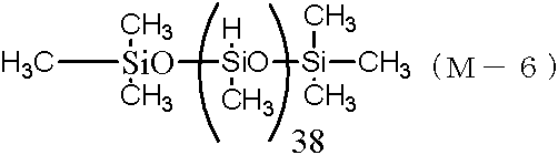
0.5モル%のビニル基を分子側鎖に有し、数平均分子量(Mn)が3万のポリジメチルシロキサン60質量部、および0.15モル%のビニル基を両末端鎖に有し、数平均分子量(Mn)が6万のポリジメチルシロキサン20質量部およびイソドデカン400質量部からなる溶液に(M-6)で示されるオルガノハイドロジェンポリシロキサンを2.5部、エチニルシクロヘキサノール0.7部を添加し混合した。さらに白金触媒CAT-PL-5(信越化学工業株式会社製)を0.5部添加し、0.2μmのメンブレンフィルターで濾過して、熱硬化性シロキサン重合体溶液(B-2)を得た。
5モル%のビニル基を両末端および側鎖に有し、数平均分子量(Mn)が3万のポリジメチルシロキサン80質量部およびイソドデカン400質量部からなる溶液に(M-6)で示されるオルガノハイドロジェンポリシロキサン7.5部、エチニルシクロヘキサノール0.7部を添加し混合した。さらに白金触媒CAT-PL-5(信越化学工業株式会社製)を0.5部添加し、0.2μmのメンブレンフィルターで濾過して、熱硬化性シロキサン重合体溶液(B-3)を得た。
4つ口フラスコに、下記式(7)で示される分子鎖両末端が水酸基で封鎖された生ゴム状のジメチルポリシロキサンであって、その30%トルエン溶液の25℃における粘度が98,000mPa・sであるジメチルポリシロキサン90部と、(CH3)3SiO1/2単位0.75モルとSiO4/2単位1モルの割合からなり、かつ固形分100部中に1.0モル%の水酸基を含むメチルポリシロキサンレジン10部とを、トルエン900部に溶解した。得られた溶液に、28%のアンモニア水を1部添加し、室温にて24時間撹拌して縮合反応させた。次いで、減圧状態で180℃に加熱し、トルエン、縮合水、アンモニア等を除去させて、固形化された部分縮合物を得た。この部分縮合物100部に、トルエン900部を加えて、溶解させた。この溶液にヘキサメチルジシラザン20部を加え、130℃にて3時間撹拌して残存する水酸基を封鎖した。次いで、減圧状態で180℃に加熱し、溶剤等を除去させて、固形化された非反応性部分縮合物を得た。更に、上記非反応性部分縮合物100部にヘキサン900部を加えて溶解させた後、これを2000部のアセトン中に投入し、析出した樹脂を回収して、その後、真空下でヘキサン等を除去して、分子量740以下の低分子量成分が0.05質量%である、重量平均分子量900,000のジメチルポリシロキサン重合体を得た。
この重合体20gをイソドデカン80gに溶解し、0.2μmのメンブレンフィルターで濾過して、ジメチルポリシロキサン重合体のイソドデカン溶液(D-1)を得た。
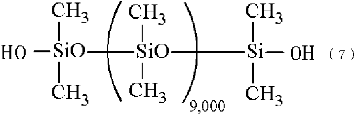
表面に高さ10μm、直径40μmの銅ポストが全面に形成された直径200mmシリコンウエハ(厚さ:725μm)にスピンコート後、ホットプレートにて、150℃で5分間加熱することにより、(A)層に対応する材料を表1に示す膜厚で、ウエハバンプ形成面に成膜した。一方、直径200mm(厚さ:500μm)のガラス板を支持体とし、この支持体にまず(C)層に対応する重合体溶液をスピンコート、およびホットプレートにより、やはり、150℃で5分間加熱することで、表1中に記載された膜厚で、ガラス支持体上に形成した。その後、(B)層に相当する熱硬化性シロキサン重合体の溶液を、ガラス支持体上に形成された(C)層上に、やはりスピンコートすることで、表1中の膜厚で形成した。さらにその後、150℃で3分間、ホットプレート上で加熱した。このようにしてこの非シリコーン熱可塑性樹脂層(A)を有するシリコンウエハ及び、熱硬化性シロキサン変性重合体層からなる(C)層と、その(C)層上に(B)層を有するガラス板とをそれぞれ、樹脂面が合わされるように、真空貼り合わせ装置内で表1に示す条件にて貼り合わせ、ウエハ加工体を作製した。
200mmのウエハ接合は、EVG社のウエハ接合装置EVG520ISを用いて行った。接合温度は表1に記載の値、接合時のチャンバー内圧力は10-3mbar以下、荷重は5kNで実施した。接合後、一旦、180℃で1時間オーブンを用いて基板を加熱し、(B)及び(C)層の硬化を実施したのち、室温まで冷却し、その後の界面の接着状況を目視で確認し、界面での気泡などの異常が発生しなかった場合を良好と評価して「○」で示し、異常が発生した場合を不良と評価して「×」で示した。
グラインダー(DISCO製、DAG810)でダイヤモンド砥石を用いてシリコンウエハの裏面研削を行った。最終基板厚50μmまでグラインドした後、光学顕微鏡(100倍)にてクラック、剥離等の異常の有無を調べた。異常が発生しなかった場合を良好と評価して「○」で示し、異常が発生した場合を不良と評価して「×」で示した。
シリコンウエハを裏面研削した後の加工体をCVD装置に導入し、2μmのSiO2膜の生成実験を行ない、その際の外観異常の有無を調べた。外観異常が発生しなかった場合を良好と評価して「○」で示し、ボイド、ウエハ膨れ、ウエハ破損等の外観異常が発生した場合を不良と評価して「×」で示した。CVD耐性試験の条件は、以下の通りである。
装置名:プラズマCVD PD270STL(サムコ社製)
RF500W、内圧40Pa
TEOS(テトラエチルオルソシリケート):O2=20sccm:680sccm
基板の剥離性は、まず、CVD耐性試験を終えたウエハ加工体の50μmまで薄型化したウエハ側にダイシングフレームを用いてダイシングテープを貼り、このダイシングテープ面を真空吸着によって、吸着板にセットした。その後、室温にて、ガラスの1点をピンセットにて持ち上げることで、ガラス基板を剥離した。50μmのウエハを割ることなく剥離できた場合を「○」で示し、割れなどの異常が発生した場合を不良と評価して「×」で示した。
上記剥離性試験終了後のダイシングテープを介してダイシングフレームに装着された200mmウエハ(CVD耐性試験条件に晒されたもの)を、接着層を上にしてスピンコーターにセットし、洗浄溶剤としてp-メンタンを5分間噴霧したのち、ウエハを回転させながらイソプロピルアルコール(IPA)を噴霧にてリンスを行った。その後、外観を観察して残存する接着材樹脂の有無を目視でチェックした。樹脂の残存が認められないものを良好と評価して「○」で示し、樹脂の残存が認められたものを不良と評価して「×」で示した。
直径200mmシリコンウエハ(厚さ:725μm)にスピンコート後、ホットプレートにて、150℃で5分間加熱することにより、(A)層に対応する材料を表1に示す膜厚で、ウエハバンプ形成面に成膜した。その後、(B)層に相当する熱硬化性シロキサン重合体の溶液を、シリコンウエハ上に形成された(A)層上に、やはりスピンコートし、さらにその後、150℃で3分間、ホットプレート上で加熱して2μm膜厚で形成した。さらに(B)層上に(C)層に対応する重合体溶液をスピンコート、およびホットプレートにより、やはり、150℃で5分間加熱することで、50μm膜厚で、シリコンウエハ上に形成した。その後オーブンで180℃で1時間かけて硬化させた。
その後、上記ウエハの(C)層上に150mm長×25mm幅のポリイミドテープを5本貼り付け、テープが張られていない部分の仮接着材層を除去した。島津製作所社のAUTOGRAPH(AG-1)を用いて300mm/分の速度でテープの一端から180°剥離で120mm剥がし、そのときにかかる力の平均(120mmストローク×5回)を、その(B)仮接着層の剥離力とした。
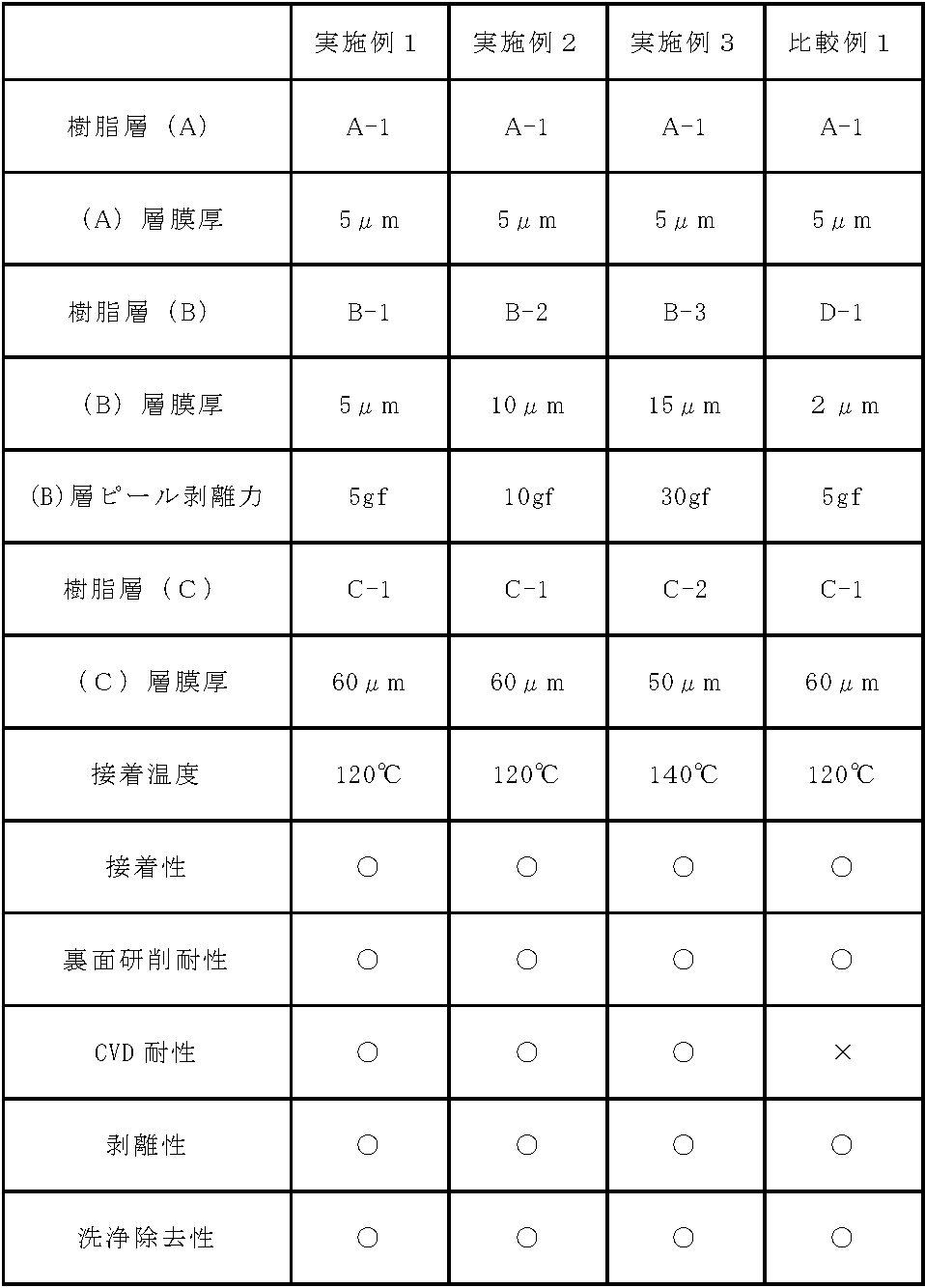
Claims (13)
- 表面に回路面を有し、裏面を加工すべきウエハを支持体に仮接着するためのウエハ加工用仮接着材であって、
前記ウエハの表面に剥離可能に接着可能な非シリコーン熱可塑性樹脂層(A)からなる第一仮接着層と、該第一仮接着層に積層された熱硬化性シロキサン重合体層(B)からなる第二仮接着層と、該第二仮接着層に積層され、前記支持体に剥離可能に接着可能な熱硬化性シロキサン変性重合体層(C)からなる第三仮接着層の3層構造を有する複合仮接着材層を備えたものであることを特徴とするウエハ加工用仮接着材。 - 前記熱硬化性シロキサン重合体層(B)が、
(B-1)1分子中に2個以上のアルケニル基を有するオルガノポリシロキサン、
(B-2)1分子中に2個以上のケイ素原子に結合した水素原子(Si-H基)を含有するオルガノハイドロジェンポリシロキサン:前記(B-1)成分中のアルケニル基に対する(B-2)成分中のSi-H基のモル比が0.3から10となる量、
(B-3)白金系触媒、
を含有する組成物の硬化物層であることを特徴とする請求項1に記載のウエハ加工用仮接着材。 - 前記熱硬化性シロキサン重合体層(B)が、更に、(B-4)成分として反応制御剤:前記(B-1)および前記(B-2)成分の合計100質量部に対して0.1から10質量部、
を含有するものであることを特徴とする請求項2に記載のウエハ加工用仮接着材。 - 前記熱硬化性シロキサン重合体層(B)の熱硬化後における25mm幅の試験片の180°ピール剥離力が2gf以上50gf以下であることを特徴とする請求項1から請求項3のいずれか1項に記載のウエハ加工用仮接着材。
- 前記熱硬化性シロキサン変性重合体層(C)が、下記一般式(1)で示される繰り返し単位を有する重量平均分子量が3,000~500,000のシロキサン結合含有重合体100質量部に対して、架橋剤としてホルマリン又はホルマリン-アルコールにより変性されたアミノ縮合物、メラミン樹脂、尿素樹脂、1分子中に平均して2個以上のメチロール基又はアルコキシメチロール基を有するフェノール化合物、及び1分子中に平均して2個以上のエポキシ基を有するエポキシ化合物から選ばれるいずれか1種以上を0.1~50質量部含有する組成物の硬化物層であることを特徴とする請求項1から請求項4のいずれか1項に記載のウエハ加工用仮接着材。


- 前記熱硬化性シロキサン変性重合体層(C)が、下記一般式(3)で示される繰り返し単位を有する重量平均分子量が3,000~500,000のシロキサン結合含有重合体100質量部に対して、架橋剤として1分子中に平均して2個以上のフェノール基を有するフェノール化合物、及び1分子中に平均して2個以上のエポキシ基を有するエポキシ化合物から選ばれるいずれか1種以上を0.1~50質量部含有する組成物の硬化物層であることを特徴とする請求項1から請求項4のいずれか1項に記載のウエハ加工用仮接着材。


- (a)表面に回路形成面及び裏面に回路非形成面を有するウエハの前記回路形成面を、請求項1から請求項6のいずれか1項に記載のウエハ加工用仮接着材に用いられる前記非シリコーン熱可塑性樹脂層(A)と、前記熱硬化性シロキサン重合体層(B)と、前記熱硬化性シロキサン変性重合体層(C)とからなる仮接着材層を介して、支持体に接合する際に、前記支持体上に形成された前記熱硬化性シロキサン変性重合体層(C)の上に前記熱硬化性シロキサン重合体層(B)を形成した後、該重合体層(C)と(B)の形成された支持体と、前記樹脂層(A)の形成された回路付きウエハとを真空下で貼り合わせる工程と、
(b)前記重合体層(B)及び(C)を熱硬化させる工程と、
(c)前記支持体と接合した前記ウエハの回路非形成面を研削又は研磨する工程と、
(d)前記ウエハの回路非形成面に加工を施す工程と、
(e)前記加工を施したウエハを前記支持体から剥離する工程と、
を含むことを特徴とする薄型ウエハの製造方法。 - 支持体上に仮接着材層が形成され、かつ仮接着材層上に、表面に回路面を有し、裏面を加工すべきウエハが積層されてなるウエハ加工体であって、
前記仮接着材層が、前記ウエハの表面に剥離可能に接着された非シリコーン熱可塑性樹脂層(A)からなる第一仮接着層と、該第一仮接着層に積層された熱硬化性シロキサン重合体層(B)からなる第二仮接着層と、該第二仮接着層に積層され、前記支持体に剥離可能に接着された熱硬化性シロキサン変性重合体層(C)からなる第三仮接着層との3層構造を有する複合仮接着材層を備えたものであることを特徴とするウエハ加工体。 - 前記熱硬化性シロキサン重合体層(B)が、
(B-1)1分子中に2個以上のアルケニル基を有するオルガノポリシロキサン、
(B-2)1分子中に2個以上のケイ素原子に結合した水素原子(Si-H基)を含有するオルガノハイドロジェンポリシロキサン:前記(B-1)成分中のアルケニル基に対する(B-2)成分中のSi-H基のモル比が0.3から10となる量、
(B-3)白金系触媒、
を含有する組成物の硬化物層であることを特徴とする請求項8に記載のウエハ加工体。 - 前記熱硬化性シロキサン重合体層(B)が、更に、(B-4)成分として反応制御剤:前記(B-1)および前記(B-2)成分の合計100質量部に対して0.1から10質量部、
を含有するものであることを特徴とする請求項9に記載のウエハ加工体。 - 前記熱硬化性シロキサン重合体層(B)の熱硬化後における25mm幅の試験片の180°ピール剥離力が2gf以上50gf以下であることを特徴とする請求項8から請求項10のいずれか1項に記載のウエハ加工体。
- 前記熱硬化性シロキサン変性重合体層(C)が、下記一般式(1)で示される繰り返し単位を有する重量平均分子量が3,000~500,000のシロキサン結合含有重合体100質量部に対して、架橋剤としてホルマリン又はホルマリン-アルコールにより変性されたアミノ縮合物、メラミン樹脂、尿素樹脂、1分子中に平均して2個以上のメチロール基又はアルコキシメチロール基を有するフェノール化合物、及び1分子中に平均して2個以上のエポキシ基を有するエポキシ化合物から選ばれるいずれか1種以上を0.1~50質量部含有する組成物の硬化物層であることを特徴とする請求項8から請求項11のいずれか1項に記載のウエハ加工体。


- 前記熱硬化性シロキサン変性重合体層(C)が、下記一般式(3)で示される繰り返し単位を有する重量平均分子量が3,000~500,000のシロキサン結合含有重合体100質量部に対して、架橋剤として1分子中に平均して2個以上のフェノール基を有するフェノール化合物、及び1分子中に平均して2個以上のエポキシ基を有するエポキシ化合物から選ばれるいずれか1種以上を0.1~50質量部含有する組成物の硬化物層であることを特徴とする請求項8から請求項11のいずれか1項に記載のウエハ加工体。


Priority Applications (4)
| Application Number | Priority Date | Filing Date | Title |
|---|---|---|---|
| EP15764462.6A EP3121838B1 (en) | 2014-03-18 | 2015-03-03 | Wafer processing laminate, temporary adhesive material for wafer processing, and method for manufacturing thin wafer |
| KR1020167025430A KR102030759B1 (ko) | 2014-03-18 | 2015-03-03 | 웨이퍼 가공체, 웨이퍼 가공용 가접착재, 및 박형 웨이퍼의 제조방법 |
| US15/122,493 US10242902B2 (en) | 2014-03-18 | 2015-03-03 | Wafer processing laminate, temporary adhesive material for wafer processing, and method for manufacturing thin wafer |
| CN201580014475.9A CN106104765B (zh) | 2014-03-18 | 2015-03-03 | 晶片加工体、晶片加工用暂时粘着材料以及薄型晶片的制造方法 |
Applications Claiming Priority (2)
| Application Number | Priority Date | Filing Date | Title |
|---|---|---|---|
| JP2014-055370 | 2014-03-18 | ||
| JP2014055370A JP6023737B2 (ja) | 2014-03-18 | 2014-03-18 | ウエハ加工体、ウエハ加工用仮接着材、及び薄型ウエハの製造方法 |
Publications (1)
| Publication Number | Publication Date |
|---|---|
| WO2015141156A1 true WO2015141156A1 (ja) | 2015-09-24 |
Family
ID=54144147
Family Applications (1)
| Application Number | Title | Priority Date | Filing Date |
|---|---|---|---|
| PCT/JP2015/001099 Ceased WO2015141156A1 (ja) | 2014-03-18 | 2015-03-03 | ウエハ加工体、ウエハ加工用仮接着材、及び薄型ウエハの製造方法 |
Country Status (7)
| Country | Link |
|---|---|
| US (1) | US10242902B2 (ja) |
| EP (1) | EP3121838B1 (ja) |
| JP (1) | JP6023737B2 (ja) |
| KR (1) | KR102030759B1 (ja) |
| CN (1) | CN106104765B (ja) |
| TW (1) | TWI663232B (ja) |
| WO (1) | WO2015141156A1 (ja) |
Cited By (1)
| Publication number | Priority date | Publication date | Assignee | Title |
|---|---|---|---|---|
| CN106800909A (zh) * | 2015-11-26 | 2017-06-06 | 信越化学工业株式会社 | 晶片层合体和制备方法 |
Families Citing this family (23)
| Publication number | Priority date | Publication date | Assignee | Title |
|---|---|---|---|---|
| JP6023737B2 (ja) * | 2014-03-18 | 2016-11-09 | 信越化学工業株式会社 | ウエハ加工体、ウエハ加工用仮接着材、及び薄型ウエハの製造方法 |
| CN204014250U (zh) * | 2014-05-16 | 2014-12-10 | 奥特斯(中国)有限公司 | 用于生产电子元件的连接系统的半成品 |
| JP6193813B2 (ja) * | 2014-06-10 | 2017-09-06 | 信越化学工業株式会社 | ウエハ加工用仮接着材料、ウエハ加工体及びこれらを使用する薄型ウエハの製造方法 |
| JP6225894B2 (ja) * | 2014-12-24 | 2017-11-08 | 信越化学工業株式会社 | ウエハの仮接着方法及び薄型ウエハの製造方法 |
| JP6325432B2 (ja) * | 2014-12-25 | 2018-05-16 | 信越化学工業株式会社 | ウエハ加工体、ウエハ加工用仮接着材、及び薄型ウエハの製造方法 |
| JP6443241B2 (ja) * | 2015-06-30 | 2018-12-26 | 信越化学工業株式会社 | ウエハ加工用仮接着材、ウエハ加工体、及び薄型ウエハの製造方法 |
| JP2017092138A (ja) * | 2015-11-05 | 2017-05-25 | Jsr株式会社 | 基材の処理方法、積層体、半導体装置およびその製造方法、ならびに仮固定用組成物 |
| JP6463664B2 (ja) | 2015-11-27 | 2019-02-06 | 信越化学工業株式会社 | ウエハ加工体及びウエハ加工方法 |
| US10074626B2 (en) * | 2016-06-06 | 2018-09-11 | Shin-Etsu Chemical Co., Ltd. | Wafer laminate and making method |
| KR102680736B1 (ko) * | 2016-12-14 | 2024-07-03 | 삼성전자주식회사 | 기판 가공 방법 및 접착층 세정 조성물 |
| JP6644719B2 (ja) | 2017-01-19 | 2020-02-12 | Jfeケミカル株式会社 | フルオレニリデンジアリルフェノール類の製造方法およびフルオレニリデンジアリルフェノール類 |
| JP6788549B2 (ja) * | 2017-06-05 | 2020-11-25 | 信越化学工業株式会社 | 基板加工用仮接着フィルムロール、薄型基板の製造方法 |
| JP7045765B2 (ja) * | 2018-04-16 | 2022-04-01 | 信越化学工業株式会社 | 回路付基板加工体及び回路付基板加工方法 |
| JP6998838B2 (ja) * | 2018-06-04 | 2022-01-18 | 信越化学工業株式会社 | 薄型基板の製造方法 |
| JP6947132B2 (ja) * | 2018-07-13 | 2021-10-13 | 信越化学工業株式会社 | ウエハ加工用仮接着剤、ウエハ積層体、ウエハ積層体の製造方法、及び薄型ウエハの製造方法 |
| JP7220135B2 (ja) * | 2018-11-01 | 2023-02-09 | 信越化学工業株式会社 | 積層体の製造方法、及び基板の製造方法 |
| SG11202105574YA (en) * | 2018-11-28 | 2021-06-29 | Nissan Chemical Corp | Adhesive agent composition, layered product and production method for layered product, and method for reducing thickness of semiconductor forming substrate |
| CN113544227B (zh) * | 2019-02-21 | 2023-06-23 | 耐克创新有限合伙公司 | 包括结合层的复合结构和制造该复合结构的方法 |
| JP7454922B2 (ja) * | 2019-07-11 | 2024-03-25 | 信越化学工業株式会社 | 基板加工用仮接着材料及び積層体の製造方法 |
| US12322637B2 (en) * | 2019-09-30 | 2025-06-03 | Shin-Etsu Chemical Co., Ltd. | Wafer processing laminate, temporary adhesive material for wafer processing, and method for manufacturing thin wafer |
| CN115485814B (zh) * | 2020-04-30 | 2026-01-23 | 信越化学工业株式会社 | 晶片加工用临时粘接剂、晶片层叠体以及薄型晶片的制造方法 |
| CN111592832B (zh) * | 2020-05-29 | 2022-06-07 | 南通通富微电子有限公司 | Daf膜及其制备方法、芯片封装结构 |
| CN116855182A (zh) * | 2023-06-21 | 2023-10-10 | 中山大学南昌研究院 | 一种热解双面胶在提高深硅刻蚀均一性中的应用 |
Citations (5)
| Publication number | Priority date | Publication date | Assignee | Title |
|---|---|---|---|---|
| JP2008532313A (ja) * | 2005-03-01 | 2008-08-14 | ダウ・コーニング・コーポレイション | 半導体加工のための一時的なウェハ結合法 |
| JP2012033737A (ja) * | 2010-07-30 | 2012-02-16 | Shin Etsu Polymer Co Ltd | 半導体ウェーハの取り扱い方法 |
| JP2013110391A (ja) * | 2011-10-28 | 2013-06-06 | Shin Etsu Chem Co Ltd | ウエハ加工体、ウエハ加工用部材、ウエハ加工用仮接着材、及び薄型ウエハの製造方法 |
| JP2013232459A (ja) * | 2012-04-27 | 2013-11-14 | Shin Etsu Chem Co Ltd | ウエハ加工体、ウエハ加工用部材、ウエハ加工用仮接着材、及び薄型ウエハの製造方法 |
| JP2013243350A (ja) * | 2012-04-24 | 2013-12-05 | Shin Etsu Chem Co Ltd | ウエハ加工体、ウエハ加工用部材、ウエハ加工用仮接着材、及び薄型ウエハの製造方法 |
Family Cites Families (62)
| Publication number | Priority date | Publication date | Assignee | Title |
|---|---|---|---|---|
| US3528940A (en) * | 1966-12-15 | 1970-09-15 | Gen Electric | Silicone pressure-sensitive adhesive of improved strength |
| US3983298A (en) * | 1975-04-18 | 1976-09-28 | Dow Corning Corporation | Polyorganosiloxane pressure sensitive adhesives and articles therefrom |
| US5216069A (en) * | 1987-08-12 | 1993-06-01 | Shin-Etsu Chemical Co., Ltd. | Silicone self-adhesives comprising modified organopolysiloxanes and self-adhesive tapes |
| US5290882A (en) * | 1991-08-13 | 1994-03-01 | Shin-Etsu Chemical Co., Ltd. | Thermosetting resin compositions |
| JP3580358B2 (ja) * | 2000-06-23 | 2004-10-20 | 信越化学工業株式会社 | 熱伝導性シリコーン組成物及び半導体装置 |
| JP3580366B2 (ja) * | 2001-05-01 | 2004-10-20 | 信越化学工業株式会社 | 熱伝導性シリコーン組成物及び半導体装置 |
| JP4565804B2 (ja) | 2002-06-03 | 2010-10-20 | スリーエム イノベイティブ プロパティズ カンパニー | 被研削基材を含む積層体、その製造方法並びに積層体を用いた極薄基材の製造方法及びそのための装置 |
| US7534498B2 (en) | 2002-06-03 | 2009-05-19 | 3M Innovative Properties Company | Laminate body, method, and apparatus for manufacturing ultrathin substrate using the laminate body |
| AU2003299296A1 (en) * | 2002-11-29 | 2004-06-23 | Fraunhofer-Gesellschaft Zur Forderung Der Angewandten Forschung E.V. | Method and device for machining a wafer, in addition to a wafer comprising a separation layer and a support layer |
| JP2006328104A (ja) | 2005-05-23 | 2006-12-07 | Jsr Corp | 接着剤組成物 |
| JP2007150065A (ja) * | 2005-11-29 | 2007-06-14 | Shin Etsu Chem Co Ltd | ダイシング・ダイボンド用接着テープ |
| JP5063016B2 (ja) * | 2006-03-23 | 2012-10-31 | リンテック株式会社 | 粘着シート及び剥離シート |
| JP5117713B2 (ja) * | 2006-12-25 | 2013-01-16 | 東レ・ダウコーニング株式会社 | シリコーン系感圧接着剤組成物および粘着テープ |
| WO2008098404A2 (en) * | 2007-02-16 | 2008-08-21 | ETH Zürich | Method for manufacturing a single-crystal film, and integrated optical device comprising such a single-crystal film |
| JP5283346B2 (ja) * | 2007-04-10 | 2013-09-04 | 信越化学工業株式会社 | 熱伝導性硬化物及びその製造方法 |
| KR100910672B1 (ko) * | 2007-08-03 | 2009-08-04 | 도레이새한 주식회사 | 내열성 점착시트 |
| CN101855080B (zh) * | 2007-11-08 | 2013-03-13 | 琳得科株式会社 | 剥离片材及压敏粘合剂制品 |
| JPWO2009069445A1 (ja) * | 2007-11-26 | 2011-04-07 | リンテック株式会社 | 剥離シート及び粘着体 |
| JP2009256400A (ja) * | 2008-04-11 | 2009-11-05 | Shin Etsu Chem Co Ltd | 半導体素子用シリコーン接着剤 |
| US8753712B2 (en) * | 2008-12-31 | 2014-06-17 | 3M Innovative Properties Company | Method of producing a component of a device, and the resulting components and devices |
| JP5413340B2 (ja) * | 2009-09-30 | 2014-02-12 | 信越化学工業株式会社 | エポキシ基含有高分子化合物、これを用いた光硬化性樹脂組成物、パターン形成方法及び電気・電子部品保護用皮膜 |
| JP5010668B2 (ja) * | 2009-12-03 | 2012-08-29 | 信越化学工業株式会社 | 積層型半導体集積装置の製造方法 |
| US8530027B2 (en) * | 2010-12-15 | 2013-09-10 | The Boeing Company | Fibers with interlocking shapes |
| PT2657300E (pt) * | 2010-12-22 | 2016-01-20 | Momentive Performance Mat Jp | Composição de poliorganossiloxano termocurável e a sua utilização |
| JP5348147B2 (ja) * | 2011-01-11 | 2013-11-20 | 信越化学工業株式会社 | 仮接着材組成物、及び薄型ウエハの製造方法 |
| WO2012118700A1 (en) * | 2011-02-28 | 2012-09-07 | Dow Corning Corporation | Wafer bonding system and method for bonding and debonding thereof |
| JP5409695B2 (ja) * | 2011-04-26 | 2014-02-05 | 信越化学工業株式会社 | オルガノポリシロキサン、オルガノポリシロキサンを含む仮接着剤組成物、及びそれを用いた薄型ウエハの製造方法 |
| JP5846060B2 (ja) * | 2011-07-27 | 2016-01-20 | 信越化学工業株式会社 | ウエハ加工体、ウエハ加工用部材、ウエハ加工用仮接着材、及び薄型ウエハの製造方法 |
| US20130084459A1 (en) * | 2011-09-30 | 2013-04-04 | 3M Innovative Properties Company | Low peel adhesive |
| US8999817B2 (en) | 2012-02-28 | 2015-04-07 | Shin-Etsu Chemical Co., Ltd. | Wafer process body, wafer processing member, wafer processing temporary adhesive material, and method for manufacturing thin wafer |
| JP5783128B2 (ja) * | 2012-04-24 | 2015-09-24 | 信越化学工業株式会社 | 加熱硬化型熱伝導性シリコーングリース組成物 |
| JP5767161B2 (ja) * | 2012-05-08 | 2015-08-19 | 信越化学工業株式会社 | ウエハ加工用仮接着材、それを用いたウエハ加工用部材、ウエハ加工体、及び薄型ウエハの作製方法 |
| US9583453B2 (en) * | 2012-05-30 | 2017-02-28 | Ormet Circuits, Inc. | Semiconductor packaging containing sintering die-attach material |
| JP5937426B2 (ja) * | 2012-05-30 | 2016-06-22 | 帝人株式会社 | 接着用構成体 |
| US20130334366A1 (en) * | 2012-06-14 | 2013-12-19 | The Boeing Company | Formation of a shaped fiber with simultaneous matrix application |
| US9114589B2 (en) * | 2012-06-14 | 2015-08-25 | The Boeing Company | Bicomponent fibers containing nano-filaments for use in optically transparent composites |
| US20140120356A1 (en) * | 2012-06-18 | 2014-05-01 | Ormet Circuits, Inc. | Conductive film adhesive |
| JP6277616B2 (ja) * | 2012-07-23 | 2018-02-14 | セントラル硝子株式会社 | 接着性組成物およびその接着方法、および接着後の剥離方法 |
| US8941215B2 (en) * | 2012-09-24 | 2015-01-27 | LuxVue Technology Corporation | Micro device stabilization post |
| JP5975528B2 (ja) * | 2012-10-11 | 2016-08-23 | 信越化学工業株式会社 | ウエハ加工体、ウエハ加工用部材、ウエハ加工用仮接着材、及び薄型ウエハの製造方法 |
| JP6059631B2 (ja) * | 2012-11-30 | 2017-01-11 | 信越化学工業株式会社 | ウエハ加工体、ウエハ加工用部材、ウエハ加工用仮接着材、及び薄型ウエハの製造方法 |
| KR102077248B1 (ko) * | 2013-01-25 | 2020-02-13 | 삼성전자주식회사 | 기판 가공 방법 |
| JP6405556B2 (ja) * | 2013-07-31 | 2018-10-17 | リンテック株式会社 | 保護膜形成フィルム、保護膜形成用シートおよび検査方法 |
| JP6569036B2 (ja) * | 2013-10-17 | 2019-09-04 | ダウ・東レ株式会社 | 硬化性シリコーン組成物および光半導体装置 |
| JP6217590B2 (ja) * | 2013-11-05 | 2017-10-25 | 信越化学工業株式会社 | 紫外線硬化性接着性オルガノポリシロキサン組成物 |
| KR102045519B1 (ko) * | 2013-11-12 | 2019-11-18 | 신에쓰 가가꾸 고교 가부시끼가이샤 | 실리콘 접착제 조성물 및 고체 촬상 디바이스 |
| KR102204589B1 (ko) * | 2013-11-26 | 2021-01-18 | 제이에스알 가부시끼가이샤 | 적층체, 기재의 처리 방법, 가고정용 조성물 및 반도체 장치 |
| EP3101681B1 (en) * | 2014-01-29 | 2020-03-25 | Shin-Etsu Chemical Co., Ltd. | Wafer workpiece, provisional adhesive material for wafer working, and thin wafer manufacturing method |
| KR20150092675A (ko) * | 2014-02-05 | 2015-08-13 | 삼성전자주식회사 | 반도체 소자의 제조 방법 |
| JP6168002B2 (ja) * | 2014-02-27 | 2017-07-26 | 信越化学工業株式会社 | 基材密着性に優れるシリコーン粘着剤組成物及び粘着性物品 |
| JP6023737B2 (ja) * | 2014-03-18 | 2016-11-09 | 信越化学工業株式会社 | ウエハ加工体、ウエハ加工用仮接着材、及び薄型ウエハの製造方法 |
| JP6156443B2 (ja) * | 2014-08-13 | 2017-07-05 | Jsr株式会社 | 積層体および基材の処理方法 |
| US9587076B2 (en) * | 2014-09-23 | 2017-03-07 | The Boeing Company | Polymer nanoparticles for controlling resin reaction rates |
| US10072126B2 (en) * | 2014-09-23 | 2018-09-11 | The Boeing Company | Soluble nanoparticles for composite performance enhancement |
| US9327458B2 (en) * | 2014-09-30 | 2016-05-03 | The Boeing Company | In-situ annealing of polymer fibers |
| JP6225894B2 (ja) * | 2014-12-24 | 2017-11-08 | 信越化学工業株式会社 | ウエハの仮接着方法及び薄型ウエハの製造方法 |
| JP6325432B2 (ja) * | 2014-12-25 | 2018-05-16 | 信越化学工業株式会社 | ウエハ加工体、ウエハ加工用仮接着材、及び薄型ウエハの製造方法 |
| JP6443241B2 (ja) * | 2015-06-30 | 2018-12-26 | 信越化学工業株式会社 | ウエハ加工用仮接着材、ウエハ加工体、及び薄型ウエハの製造方法 |
| JP6589766B2 (ja) * | 2015-08-18 | 2019-10-16 | 信越化学工業株式会社 | ウエハ加工用接着材、ウエハ積層体及び薄型ウエハの製造方法 |
| JP6588404B2 (ja) * | 2015-10-08 | 2019-10-09 | 信越化学工業株式会社 | 仮接着方法及び薄型ウエハの製造方法 |
| JP6502824B2 (ja) * | 2015-10-19 | 2019-04-17 | 信越化学工業株式会社 | ウエハ加工体、ウエハ加工用仮接着材、及び薄型ウエハの製造方法 |
| JP6791086B2 (ja) * | 2016-10-11 | 2020-11-25 | 信越化学工業株式会社 | ウエハ積層体、その製造方法、及びウエハ積層用接着剤組成物 |
-
2014
- 2014-03-18 JP JP2014055370A patent/JP6023737B2/ja active Active
-
2015
- 2015-03-03 WO PCT/JP2015/001099 patent/WO2015141156A1/ja not_active Ceased
- 2015-03-03 US US15/122,493 patent/US10242902B2/en active Active
- 2015-03-03 CN CN201580014475.9A patent/CN106104765B/zh active Active
- 2015-03-03 EP EP15764462.6A patent/EP3121838B1/en active Active
- 2015-03-03 KR KR1020167025430A patent/KR102030759B1/ko active Active
- 2015-03-16 TW TW104108323A patent/TWI663232B/zh active
Patent Citations (5)
| Publication number | Priority date | Publication date | Assignee | Title |
|---|---|---|---|---|
| JP2008532313A (ja) * | 2005-03-01 | 2008-08-14 | ダウ・コーニング・コーポレイション | 半導体加工のための一時的なウェハ結合法 |
| JP2012033737A (ja) * | 2010-07-30 | 2012-02-16 | Shin Etsu Polymer Co Ltd | 半導体ウェーハの取り扱い方法 |
| JP2013110391A (ja) * | 2011-10-28 | 2013-06-06 | Shin Etsu Chem Co Ltd | ウエハ加工体、ウエハ加工用部材、ウエハ加工用仮接着材、及び薄型ウエハの製造方法 |
| JP2013243350A (ja) * | 2012-04-24 | 2013-12-05 | Shin Etsu Chem Co Ltd | ウエハ加工体、ウエハ加工用部材、ウエハ加工用仮接着材、及び薄型ウエハの製造方法 |
| JP2013232459A (ja) * | 2012-04-27 | 2013-11-14 | Shin Etsu Chem Co Ltd | ウエハ加工体、ウエハ加工用部材、ウエハ加工用仮接着材、及び薄型ウエハの製造方法 |
Cited By (2)
| Publication number | Priority date | Publication date | Assignee | Title |
|---|---|---|---|---|
| CN106800909A (zh) * | 2015-11-26 | 2017-06-06 | 信越化学工业株式会社 | 晶片层合体和制备方法 |
| CN106800909B (zh) * | 2015-11-26 | 2021-05-28 | 信越化学工业株式会社 | 晶片层合体和制备方法 |
Also Published As
| Publication number | Publication date |
|---|---|
| CN106104765B (zh) | 2019-05-14 |
| EP3121838B1 (en) | 2020-09-16 |
| US10242902B2 (en) | 2019-03-26 |
| US20170069521A1 (en) | 2017-03-09 |
| EP3121838A4 (en) | 2017-08-23 |
| JP6023737B2 (ja) | 2016-11-09 |
| KR102030759B1 (ko) | 2019-10-10 |
| EP3121838A1 (en) | 2017-01-25 |
| TW201546213A (zh) | 2015-12-16 |
| CN106104765A (zh) | 2016-11-09 |
| KR20160132851A (ko) | 2016-11-21 |
| JP2015179692A (ja) | 2015-10-08 |
| TWI663232B (zh) | 2019-06-21 |
Similar Documents
| Publication | Publication Date | Title |
|---|---|---|
| JP6023737B2 (ja) | ウエハ加工体、ウエハ加工用仮接着材、及び薄型ウエハの製造方法 | |
| JP6130522B2 (ja) | ウエハ加工体、ウエハ加工用仮接着材、及び薄型ウエハの製造方法 | |
| JP6325432B2 (ja) | ウエハ加工体、ウエハ加工用仮接着材、及び薄型ウエハの製造方法 | |
| JP6225894B2 (ja) | ウエハの仮接着方法及び薄型ウエハの製造方法 | |
| JP5983519B2 (ja) | ウエハ加工体、ウエハ加工用部材、ウエハ加工用仮接着材、及び薄型ウエハの製造方法 | |
| JP6404787B2 (ja) | ウエハ加工体、ウエハ加工用仮接着材、及び薄型ウエハの製造方法 | |
| JP6443241B2 (ja) | ウエハ加工用仮接着材、ウエハ加工体、及び薄型ウエハの製造方法 | |
| JP2017079245A (ja) | ウエハ加工体、ウエハ加工用仮接着材、及び薄型ウエハの製造方法 | |
| JP2018203880A (ja) | 基板加工用仮接着フィルムロール、薄型基板の製造方法 | |
| JP2023052354A (ja) | 基板加工用仮接着材料及び積層体の製造方法 | |
| CN111146133A (zh) | 层叠体的制造方法及基板的制造方法 |
Legal Events
| Date | Code | Title | Description |
|---|---|---|---|
| 121 | Ep: the epo has been informed by wipo that ep was designated in this application |
Ref document number: 15764462 Country of ref document: EP Kind code of ref document: A1 |
|
| WWE | Wipo information: entry into national phase |
Ref document number: 15122493 Country of ref document: US |
|
| ENP | Entry into the national phase |
Ref document number: 20167025430 Country of ref document: KR Kind code of ref document: A |
|
| REEP | Request for entry into the european phase |
Ref document number: 2015764462 Country of ref document: EP |
|
| WWE | Wipo information: entry into national phase |
Ref document number: 2015764462 Country of ref document: EP |
|
| NENP | Non-entry into the national phase |
Ref country code: DE |