WO2015141512A1 - 電子素子封止用積層シートおよび電子デバイスの製造方法 - Google Patents
電子素子封止用積層シートおよび電子デバイスの製造方法 Download PDFInfo
- Publication number
- WO2015141512A1 WO2015141512A1 PCT/JP2015/056881 JP2015056881W WO2015141512A1 WO 2015141512 A1 WO2015141512 A1 WO 2015141512A1 JP 2015056881 W JP2015056881 W JP 2015056881W WO 2015141512 A1 WO2015141512 A1 WO 2015141512A1
- Authority
- WO
- WIPO (PCT)
- Prior art keywords
- sealing
- sealing material
- sheet
- gas barrier
- electronic element
- Prior art date
- Legal status (The legal status is an assumption and is not a legal conclusion. Google has not performed a legal analysis and makes no representation as to the accuracy of the status listed.)
- Ceased
Links
Images




Classifications
-
- H—ELECTRICITY
- H10—SEMICONDUCTOR DEVICES; ELECTRIC SOLID-STATE DEVICES NOT OTHERWISE PROVIDED FOR
- H10F—INORGANIC SEMICONDUCTOR DEVICES SENSITIVE TO INFRARED RADIATION, LIGHT, ELECTROMAGNETIC RADIATION OF SHORTER WAVELENGTH OR CORPUSCULAR RADIATION
- H10F19/00—Integrated devices, or assemblies of multiple devices, comprising at least one photovoltaic cell covered by group H10F10/00, e.g. photovoltaic modules
- H10F19/80—Encapsulations or containers for integrated devices, or assemblies of multiple devices, having photovoltaic cells
- H10F19/804—Materials of encapsulations
-
- H—ELECTRICITY
- H10—SEMICONDUCTOR DEVICES; ELECTRIC SOLID-STATE DEVICES NOT OTHERWISE PROVIDED FOR
- H10K—ORGANIC ELECTRIC SOLID-STATE DEVICES
- H10K50/00—Organic light-emitting devices
- H10K50/80—Constructional details
- H10K50/84—Passivation; Containers; Encapsulations
- H10K50/842—Containers
- H10K50/8426—Peripheral sealing arrangements, e.g. adhesives, sealants
-
- B—PERFORMING OPERATIONS; TRANSPORTING
- B29—WORKING OF PLASTICS; WORKING OF SUBSTANCES IN A PLASTIC STATE IN GENERAL
- B29C—SHAPING OR JOINING OF PLASTICS; SHAPING OF MATERIAL IN A PLASTIC STATE, NOT OTHERWISE PROVIDED FOR; AFTER-TREATMENT OF THE SHAPED PRODUCTS, e.g. REPAIRING
- B29C48/00—Extrusion moulding, i.e. expressing the moulding material through a die or nozzle which imparts the desired form; Apparatus therefor
- B29C48/001—Combinations of extrusion moulding with other shaping operations
- B29C48/0022—Combinations of extrusion moulding with other shaping operations combined with cutting
-
- B—PERFORMING OPERATIONS; TRANSPORTING
- B29—WORKING OF PLASTICS; WORKING OF SUBSTANCES IN A PLASTIC STATE IN GENERAL
- B29C—SHAPING OR JOINING OF PLASTICS; SHAPING OF MATERIAL IN A PLASTIC STATE, NOT OTHERWISE PROVIDED FOR; AFTER-TREATMENT OF THE SHAPED PRODUCTS, e.g. REPAIRING
- B29C48/00—Extrusion moulding, i.e. expressing the moulding material through a die or nozzle which imparts the desired form; Apparatus therefor
- B29C48/15—Extrusion moulding, i.e. expressing the moulding material through a die or nozzle which imparts the desired form; Apparatus therefor incorporating preformed parts or layers, e.g. extrusion moulding around inserts
- B29C48/154—Coating solid articles, i.e. non-hollow articles
-
- B—PERFORMING OPERATIONS; TRANSPORTING
- B32—LAYERED PRODUCTS
- B32B—LAYERED PRODUCTS, i.e. PRODUCTS BUILT-UP OF STRATA OF FLAT OR NON-FLAT, e.g. CELLULAR OR HONEYCOMB, FORM
- B32B37/00—Methods or apparatus for laminating, e.g. by curing or by ultrasonic bonding
- B32B37/12—Methods or apparatus for laminating, e.g. by curing or by ultrasonic bonding characterised by using adhesives
-
- B—PERFORMING OPERATIONS; TRANSPORTING
- B32—LAYERED PRODUCTS
- B32B—LAYERED PRODUCTS, i.e. PRODUCTS BUILT-UP OF STRATA OF FLAT OR NON-FLAT, e.g. CELLULAR OR HONEYCOMB, FORM
- B32B38/00—Ancillary operations in connection with laminating processes
- B32B38/0004—Cutting, tearing or severing, e.g. bursting; Cutter details
-
- H—ELECTRICITY
- H05—ELECTRIC TECHNIQUES NOT OTHERWISE PROVIDED FOR
- H05B—ELECTRIC HEATING; ELECTRIC LIGHT SOURCES NOT OTHERWISE PROVIDED FOR; CIRCUIT ARRANGEMENTS FOR ELECTRIC LIGHT SOURCES, IN GENERAL
- H05B33/00—Electroluminescent light sources
- H05B33/02—Details
- H05B33/04—Sealing arrangements, e.g. against humidity
-
- H—ELECTRICITY
- H10—SEMICONDUCTOR DEVICES; ELECTRIC SOLID-STATE DEVICES NOT OTHERWISE PROVIDED FOR
- H10F—INORGANIC SEMICONDUCTOR DEVICES SENSITIVE TO INFRARED RADIATION, LIGHT, ELECTROMAGNETIC RADIATION OF SHORTER WAVELENGTH OR CORPUSCULAR RADIATION
- H10F19/00—Integrated devices, or assemblies of multiple devices, comprising at least one photovoltaic cell covered by group H10F10/00, e.g. photovoltaic modules
- H10F19/80—Encapsulations or containers for integrated devices, or assemblies of multiple devices, having photovoltaic cells
-
- H—ELECTRICITY
- H10—SEMICONDUCTOR DEVICES; ELECTRIC SOLID-STATE DEVICES NOT OTHERWISE PROVIDED FOR
- H10K—ORGANIC ELECTRIC SOLID-STATE DEVICES
- H10K30/00—Organic devices sensitive to infrared radiation, light, electromagnetic radiation of shorter wavelength or corpuscular radiation
- H10K30/80—Constructional details
- H10K30/88—Passivation; Containers; Encapsulations
-
- H—ELECTRICITY
- H10—SEMICONDUCTOR DEVICES; ELECTRIC SOLID-STATE DEVICES NOT OTHERWISE PROVIDED FOR
- H10K—ORGANIC ELECTRIC SOLID-STATE DEVICES
- H10K50/00—Organic light-emitting devices
- H10K50/80—Constructional details
- H10K50/84—Passivation; Containers; Encapsulations
-
- H—ELECTRICITY
- H10—SEMICONDUCTOR DEVICES; ELECTRIC SOLID-STATE DEVICES NOT OTHERWISE PROVIDED FOR
- H10K—ORGANIC ELECTRIC SOLID-STATE DEVICES
- H10K50/00—Organic light-emitting devices
- H10K50/80—Constructional details
- H10K50/84—Passivation; Containers; Encapsulations
- H10K50/844—Encapsulations
-
- H—ELECTRICITY
- H10—SEMICONDUCTOR DEVICES; ELECTRIC SOLID-STATE DEVICES NOT OTHERWISE PROVIDED FOR
- H10K—ORGANIC ELECTRIC SOLID-STATE DEVICES
- H10K59/00—Integrated devices, or assemblies of multiple devices, comprising at least one organic light-emitting element covered by group H10K50/00
- H10K59/80—Constructional details
- H10K59/87—Passivation; Containers; Encapsulations
- H10K59/871—Self-supporting sealing arrangements
- H10K59/8722—Peripheral sealing arrangements, e.g. adhesives, sealants
-
- H—ELECTRICITY
- H10—SEMICONDUCTOR DEVICES; ELECTRIC SOLID-STATE DEVICES NOT OTHERWISE PROVIDED FOR
- H10K—ORGANIC ELECTRIC SOLID-STATE DEVICES
- H10K59/00—Integrated devices, or assemblies of multiple devices, comprising at least one organic light-emitting element covered by group H10K50/00
- H10K59/80—Constructional details
- H10K59/87—Passivation; Containers; Encapsulations
- H10K59/873—Encapsulations
-
- H—ELECTRICITY
- H10—SEMICONDUCTOR DEVICES; ELECTRIC SOLID-STATE DEVICES NOT OTHERWISE PROVIDED FOR
- H10K—ORGANIC ELECTRIC SOLID-STATE DEVICES
- H10K71/00—Manufacture or treatment specially adapted for the organic devices covered by this subclass
-
- H—ELECTRICITY
- H10—SEMICONDUCTOR DEVICES; ELECTRIC SOLID-STATE DEVICES NOT OTHERWISE PROVIDED FOR
- H10K—ORGANIC ELECTRIC SOLID-STATE DEVICES
- H10K71/00—Manufacture or treatment specially adapted for the organic devices covered by this subclass
- H10K71/80—Manufacture or treatment specially adapted for the organic devices covered by this subclass using temporary substrates
-
- B—PERFORMING OPERATIONS; TRANSPORTING
- B32—LAYERED PRODUCTS
- B32B—LAYERED PRODUCTS, i.e. PRODUCTS BUILT-UP OF STRATA OF FLAT OR NON-FLAT, e.g. CELLULAR OR HONEYCOMB, FORM
- B32B2457/00—Electrical equipment
-
- B—PERFORMING OPERATIONS; TRANSPORTING
- B32—LAYERED PRODUCTS
- B32B—LAYERED PRODUCTS, i.e. PRODUCTS BUILT-UP OF STRATA OF FLAT OR NON-FLAT, e.g. CELLULAR OR HONEYCOMB, FORM
- B32B2457/00—Electrical equipment
- B32B2457/20—Displays, e.g. liquid crystal displays, plasma displays
-
- B—PERFORMING OPERATIONS; TRANSPORTING
- B32—LAYERED PRODUCTS
- B32B—LAYERED PRODUCTS, i.e. PRODUCTS BUILT-UP OF STRATA OF FLAT OR NON-FLAT, e.g. CELLULAR OR HONEYCOMB, FORM
- B32B38/00—Ancillary operations in connection with laminating processes
- B32B38/10—Removing layers, or parts of layers, mechanically or chemically
-
- C—CHEMISTRY; METALLURGY
- C08—ORGANIC MACROMOLECULAR COMPOUNDS; THEIR PREPARATION OR CHEMICAL WORKING-UP; COMPOSITIONS BASED THEREON
- C08L—COMPOSITIONS OF MACROMOLECULAR COMPOUNDS
- C08L2203/00—Applications
- C08L2203/20—Applications use in electrical or conductive gadgets
- C08L2203/206—Applications use in electrical or conductive gadgets use in coating or encapsulating of electronic parts
-
- H—ELECTRICITY
- H05—ELECTRIC TECHNIQUES NOT OTHERWISE PROVIDED FOR
- H05B—ELECTRIC HEATING; ELECTRIC LIGHT SOURCES NOT OTHERWISE PROVIDED FOR; CIRCUIT ARRANGEMENTS FOR ELECTRIC LIGHT SOURCES, IN GENERAL
- H05B33/00—Electroluminescent light sources
- H05B33/10—Apparatus or processes specially adapted to the manufacture of electroluminescent light sources
-
- H—ELECTRICITY
- H10—SEMICONDUCTOR DEVICES; ELECTRIC SOLID-STATE DEVICES NOT OTHERWISE PROVIDED FOR
- H10K—ORGANIC ELECTRIC SOLID-STATE DEVICES
- H10K71/00—Manufacture or treatment specially adapted for the organic devices covered by this subclass
- H10K71/851—Division of substrate
-
- Y—GENERAL TAGGING OF NEW TECHNOLOGICAL DEVELOPMENTS; GENERAL TAGGING OF CROSS-SECTIONAL TECHNOLOGIES SPANNING OVER SEVERAL SECTIONS OF THE IPC; TECHNICAL SUBJECTS COVERED BY FORMER USPC CROSS-REFERENCE ART COLLECTIONS [XRACs] AND DIGESTS
- Y02—TECHNOLOGIES OR APPLICATIONS FOR MITIGATION OR ADAPTATION AGAINST CLIMATE CHANGE
- Y02E—REDUCTION OF GREENHOUSE GAS [GHG] EMISSIONS, RELATED TO ENERGY GENERATION, TRANSMISSION OR DISTRIBUTION
- Y02E10/00—Energy generation through renewable energy sources
- Y02E10/50—Photovoltaic [PV] energy
-
- Y—GENERAL TAGGING OF NEW TECHNOLOGICAL DEVELOPMENTS; GENERAL TAGGING OF CROSS-SECTIONAL TECHNOLOGIES SPANNING OVER SEVERAL SECTIONS OF THE IPC; TECHNICAL SUBJECTS COVERED BY FORMER USPC CROSS-REFERENCE ART COLLECTIONS [XRACs] AND DIGESTS
- Y02—TECHNOLOGIES OR APPLICATIONS FOR MITIGATION OR ADAPTATION AGAINST CLIMATE CHANGE
- Y02E—REDUCTION OF GREENHOUSE GAS [GHG] EMISSIONS, RELATED TO ENERGY GENERATION, TRANSMISSION OR DISTRIBUTION
- Y02E10/00—Energy generation through renewable energy sources
- Y02E10/50—Photovoltaic [PV] energy
- Y02E10/549—Organic PV cells
-
- Y—GENERAL TAGGING OF NEW TECHNOLOGICAL DEVELOPMENTS; GENERAL TAGGING OF CROSS-SECTIONAL TECHNOLOGIES SPANNING OVER SEVERAL SECTIONS OF THE IPC; TECHNICAL SUBJECTS COVERED BY FORMER USPC CROSS-REFERENCE ART COLLECTIONS [XRACs] AND DIGESTS
- Y02—TECHNOLOGIES OR APPLICATIONS FOR MITIGATION OR ADAPTATION AGAINST CLIMATE CHANGE
- Y02P—CLIMATE CHANGE MITIGATION TECHNOLOGIES IN THE PRODUCTION OR PROCESSING OF GOODS
- Y02P70/00—Climate change mitigation technologies in the production process for final industrial or consumer products
- Y02P70/50—Manufacturing or production processes characterised by the final manufactured product
Definitions
- the present invention relates to a laminated sheet for encapsulating electronic elements used for encapsulating electronic elements and a method for producing an electronic device.
- organic EL Electro Luminescence
- Such an organic EL display device is usually manufactured by sealing an organic EL element on a substrate with a sealing material.
- a sheet-like sealing material having a photocurable resin layer is attached to the entire glass substrate on which a plurality of organic EL elements are formed, and the photocurable resin is cured by ultraviolet irradiation. . Thereafter, an organic EL display device is obtained in which the organic EL element is sealed with a photocurable resin that is divided and cured for each organic EL element.
- a sealing film is formed on the entire substrate on which a plurality of organic EL elements are formed, and then a portion of the sealing film corresponding to the terminal portion of the organic EL element is formed. It is removed by laser light irradiation. Then, it divides
- the sealing film corresponding to the terminal portion of the organic EL element is removed by laser light irradiation.
- the terminal portion of the organic EL element may be damaged, or There is a possibility that the sealing film may remain in the terminal portion of the organic EL element, and there is a problem in reliability as the organic EL display device.
- the manufacturing cost is increased.
- the sealing film is formed entirely on the glass substrate, the sealing film may be damaged when divided for each organic EL element.
- the present invention has been made in view of such a situation, and an object thereof is to provide means capable of efficiently manufacturing a highly reliable electronic device.
- the present invention corresponds to a long release sheet and an electronic element which is an object to be sealed, which is laminated in a plurality of different positions on the long release sheet.
- a laminated sheet for sealing an electronic device characterized by comprising a sealing material having a shape (Invention 1).
- sheet includes the concept of a tape.
- the said electronic element can be sealed using the sealing material which has a shape corresponding to an electronic element previously, for example, of electronic elements, such as an organic EL element, It is not necessary to remove the sealing material corresponding to the terminal portion, and there is no possibility that the terminal portion of the electronic element is damaged by the removing operation, or the sealing material does not remain in the terminal portion of the electronic element. Even when a plurality of electronic elements sealed on the material are divided for each electronic element, the sealing material is not likely to be damaged. Therefore, according to the said invention (invention 1), a highly reliable electronic device can be manufactured efficiently.
- the protective material is provided in the width direction both sides of the said elongate peeling sheet,
- the said sealing material differs from the said protective material on the said elongate peeling sheet. It is preferable to be provided at a position (Invention 2).
- the thickness of the protective material is preferably equal to or thicker than the thickness of the sealing material (Invention 3).
- the protective material is preferably made of the same material as the sealing material (Invention 4).
- the gas barrier film which has the shape corresponding to the electronic element which is a to-be-sealed thing may be laminated
- the protective material is provided in the width direction both sides of the said elongate release sheet,
- the laminated body of the said sealing material and the said gas barrier film is on the said elongate release sheet.
- the protective material is preferably provided at a different position (Invention 6).
- the thickness of the protective material is preferably equal to or greater than the thickness of the laminate of the sealing material and the gas barrier film (Invention 7).
- the protective material is preferably composed of the same material as the laminate of the sealing material and the gas barrier film (Invention 8).
- a plurality of the sealing materials may be provided also in the width direction of the long release sheet (Invention 11).
- the electronic element as an object to be sealed is an organic EL element (Invention 12).
- the sealing material is selected from the group consisting of acid-modified polyolefin resins, silane-modified polyolefin resins, ionomers, ethylene- (meth) acrylic acid copolymers, and rubber resins. It is preferably composed of at least one (Invention 13).
- the laminate of the sealing material and the gas barrier film has a water vapor transmission rate of 20 g / (m in an environment of a temperature of 40 ° C. and a relative humidity of 90% RH in terms of a thickness of 50 ⁇ m. 2 ⁇ day) or less (Invention 14).
- the present invention is a method for producing the electronic device sealing laminated sheet (Invention 4), wherein one surface of the long release sheet is substantially the same size as the release sheet, and the sealing is performed. Forming a sealing material layer made of a material constituting the stopper, and half-cutting the sealing material layer so as to form the sealing material and the protective material, and removing an excess portion; A method for producing a laminated sheet for encapsulating electronic elements is provided (Invention 15).
- the present invention provides a method for producing the laminated sheet for sealing an electronic device (Invention 8), wherein one surface of the long release sheet is substantially the same size as the release sheet, and the sealing is performed.
- a sealing material layer made of a material constituting a stopper and a gas barrier material layer made of a material constituting the gas barrier film are formed so as to be laminated in that order, and the sealing material and the gas barrier film are laminated.
- a gas barrier material layer and a sealing material layer are half-cut so that the protective material is formed, and an excess portion is removed.
- the present invention provides a shape corresponding to an electronic element as an object to be sealed on the side opposite to the release sheet side of the sealing material in the electronic element sealing laminated sheet (Invention 1 to 4).
- the gas barrier film is laminated, the laminate of the sealing material and the gas barrier film is peeled off from the release sheet, and the sealing material and the gas barrier film are laminated with the sealing material being a sealed object.
- a method for manufacturing an electronic device characterized in that the electronic device is sealed so as to be in contact with a certain electronic device (Invention 17).
- the present invention provides the electronic device sealing laminated sheet (Invention 1 to 4), wherein the sealing material is superposed on an electronic device that is an object to be sealed, and the sealing material is removed from the sealing material at any stage. Peeling the release sheet, laminating a gas barrier film having a shape corresponding to the electronic element that is the object to be sealed on the side opposite to the electronic element side of the sealing material, and sealing the electronic element An electronic device manufacturing method is provided (Invention 18).
- the present invention provides a gas barrier film having a shape corresponding to an electronic element that is an object to be sealed, the sealing on the long release sheet in the laminated sheet for electronic element sealing (Inventions 1 to 4).
- a plurality of gas barrier film laminated sheets laminated on a long support sheet are prepared in the same arrangement as the stopper, and the sealing material on the long release sheet in the electronic element sealing laminated sheet;
- the gas barrier film laminated sheet is laminated with the gas barrier film on the long support sheet, the release sheet is peeled off from the sealing material, and the gas barrier film and the sealing material are laminated on the support sheet.
- the body is overlaid on the electronic element such that the sealing material contacts the electronic element that is the object to be sealed, the electronic element is sealed, and the gas barrier film is sealed at any stage.
- the present invention provides a method of laminating a long gas barrier film on the side opposite to the release sheet side of the encapsulant in the laminated sheet for encapsulating electronic elements (Inventions 1 to 4),
- the release sheet is peeled off, the sealing material on the long gas barrier film is overlaid on the electronic element, the electronic element is sealed, and the long gas barrier film is shaped to correspond to the electronic element
- the present invention provides a method for manufacturing an electronic device characterized in that unnecessary portions are removed by removing the unnecessary portion (Invention 20).
- the present invention provides a laminate of the sealing material and the gas barrier film in the laminated sheet for sealing an electronic device (Inventions 5 to 8) from the release sheet, and the sealing material and the gas barrier film Provided is a method of manufacturing an electronic device, wherein a laminate is overlaid on the electronic element so that the sealing material contacts an electronic element that is an object to be sealed, and the electronic element is sealed. (Invention 21).
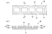
- (A) is a top view of the lamination sheet for electronic device sealing which concerns on the 1st Embodiment of this invention
- (b) is sectional drawing (A of (a) of the lamination sheet for the electronic device sealing) -A sectional view).
- (A) is a top view of the laminated sheet for electronic device sealing which concerns on the 2nd Embodiment of this invention
- (b) is sectional drawing (B of (a) of the laminated sheet for electronic device sealing -B sectional view).
- the electronic element is a sealed object.
- the type of the electronic element is not particularly limited as long as it is a sealing target, and examples thereof include an organic EL element, a liquid crystal element, a light emitting diode (LED element), an electronic paper element, a solar cell element, and the like. It is done.
- the electronic device manufactured by embodiment of this invention is an electronic device formed by sealing the above electronic elements, for example, a module for display apparatuses, a solar cell module, etc. are mentioned.
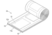
- an electronic element sealing laminated sheet 1 ⁇ / b> A includes a long first release sheet 11 a and a width on the first release sheet 11 a.
- the protective material 13 includes a second long release sheet 11b laminated on the side opposite to the first release sheet 11a side.
- “long” means that the length with respect to the width is 10 times or more.
- the electronic element sealing laminated sheet 1A according to the present embodiment is long, and is usually used by being unwound from a rolled-up state (see FIG. 1).
- the sealing material 12 has a shape corresponding to an electronic element that is an object to be sealed.
- the “shape corresponding to the electronic element” is preferably a shape that is large enough to seal the electronic element and that does not require removal of the sealing material 12 after sealing. . If the electronic device is sealed with the sealing material 12 having such a shape, for example, it is not necessary to remove a portion of the sealing material corresponding to the terminal portion of the electronic device such as an organic EL device, thereby simplifying the process. In addition, there is no fear that the terminal portion of the electronic element is damaged by the removing operation, or that the sealing material does not remain in the terminal portion of the electronic element.
- the laminated sheet 1A for encapsulating electronic elements according to this embodiment, a highly reliable electronic device can be efficiently manufactured.
- the sealing material 12 has a quadrangular shape in plan view, but is not limited to this, and may have a desired shape according to the shape of the electronic element that is the object to be sealed. it can.
- the sealing material 12 may have a circular shape in a plan view, may have a desired polygonal shape, or may have a shape in which a part thereof is cut out.
- a plurality of the sealing materials 12 are continuously provided only in the length direction of the electronic element sealing laminated sheet 1A.
- the present invention is not limited to this.
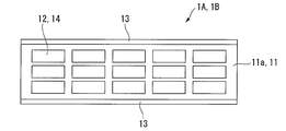
- FIG. As described above, a plurality of electronic element sealing laminated sheets 1A may be provided not only in the length direction but also in the width direction.
- the material constituting the sealing material 12 may be appropriately selected according to the type of electronic element that is the object to be sealed, and may be composed of a single layer or a plurality of layers.
- a thermoplastic resin, a thermosetting resin, an energy ray curable resin, or the like is usually used as a material constituting the sealing material 12.
- thermoplastic resins include acid-modified polyolefin resins, silane-modified polyolefin resins, ionomers, ethylene-vinyl acetate copolymers, ethylene- (meth) acrylic acid copolymers, ethylene- (meth) acrylic acid ester copolymers.
- examples include polymers, polyester resins, polyurethane resins, polyester urethane resins, acrylic resins, amide resins, styrene resins, silane resins, and rubber resins.
- acid-modified polyolefin resins silane-modified polyolefin resins, ionomers, ethylene- (meth) acrylic acid copolymers, and rubber resins, which have high adhesive strength and relatively low water vapor permeability, are preferable. These can be used individually by 1 type or in mixture of 2 or more types.
- (meth) acrylic acid means both acrylic acid and methacrylic acid. The same applies to other similar terms.
- the thickness of the sealing material 12 should just be the thickness which can seal the electronic element which is a to-be-sealed thing, and is suitably determined according to the thickness and shape of an electronic element.
- the thickness of the sealing material 12 is preferably 1 to 500 ⁇ m, particularly preferably 5 to 300 ⁇ m, and more preferably 10 to 100 ⁇ m.
- the sealing material 12 preferably has an adhesive strength to a glass plate (soda lime glass) of 3 N / 25 mm or more, particularly preferably 5 N / 25 mm or more, and more preferably 10 N / 25 mm or more. .
- a glass plate sina lime glass
- the upper limit of the adhesive force is not particularly limited, but usually it is preferably 500 N / 25 mm or less.
- the adhesive force is 24 hours after bonding, left in an environment of 23 ° C. and 50% RH, and then in that environment, using a tensile tester (Orientec Co., Tensilon), a peeling speed of 300 mm. / Min, and a value measured by performing a peel test under the condition of a peel angle of 180 °.
- the electronic element sealing laminated sheet 1A according to the present embodiment has protective materials 13 on both sides in the width direction.
- the electronic element sealing laminated sheet 1 ⁇ / b> A has such a protective material 13, so that the winding pressure applied to the sealing material 12 is reduced even when the electronic element sealing laminated sheet 1 ⁇ / b> A is rolled up.
- the protective material 13 has a long band shape, but is not limited to this shape.
- it may be a shape having a protruding portion that enters between the plurality of sealing materials 12 from a long band portion.
- it may be an intermittent strip.
- the protective material 13 is not an essential component, and the protective material 13 may be omitted from the electronic element sealing laminated sheet 1A.
- the material constituting the protective material 13 is not particularly limited as long as the above effects are exhibited.
- it may be made of the same material as the sealing material 12, may be made of a desired material that can be applied or printed, or may be made of a pressure-sensitive adhesive sheet made of a desired base material and pressure-sensitive adhesive layer.
- the sealant 12 is made of the same material and is formed simultaneously with the formation of the sealant 12. This manufacturing method will be described later.
- the thickness of the protective material 13 is preferably equal to or thicker than the thickness of the sealing material 12. Thereby, it is possible to effectively suppress the formation of winding marks and wrinkles on the sealing material 12.
- first release sheet 11a and the second release sheet 11b examples include a polyethylene film, a polypropylene film, a polybutene film, a polybutadiene film, a polymethylpentene film, a polyvinyl chloride film, a vinyl chloride copolymer film, and a polyethylene terephthalate film.
- Polycarbonate film, polyimide film, fluororesin film, cross-linked films of these, etc. are used. Moreover, these laminated films may be sufficient.
- the surface on the sealing material 12 side of the first release sheet 11a and the second release sheet 11b is subjected to a release treatment.
- the release agent used for the release treatment include alkyd, silicone, fluorine, unsaturated polyester, polyolefin, and wax release agents.
- the second release sheet 11b When using the laminated sheet 1A for encapsulating electronic elements, when the second release sheet 11b is peeled first, and the first release sheet 11a is peeled later, the second release sheet 11b is lightly peeled with a small peel force. It is preferable to use a mold release sheet and the first release sheet 11a to be a heavy release release sheet having a large release force.
- the thickness of the first release sheet 11a and the second release sheet 11b is not particularly limited, but is usually about 10 to 200 ⁇ m, preferably about 20 to 100 ⁇ m.
- the second release sheet 11b is not an essential component, and the second release sheet 11b may be omitted from the electronic element sealing laminated sheet 1A.
- the sealing material 12 is the back surface of the first release sheet 11a (the electronic element sealing laminated sheet 1A in an unwound state).
- the back surface of the first release sheet 11a is also subjected to a peeling treatment or the sealing material 12 Are formed on the surface (the surface opposite to the surface on the first release sheet 11a side of the sealing material 12 in the electronic element sealing laminated sheet 1A in an unwound state), and the sealing material 12 and the first It is preferable to reduce the contact area with the back surface of one release sheet 11a.
- the unevenness on the surface of the sealing material 12 can be formed by, for example, embossing.
- the shape of the unevenness is not particularly limited as long as the sealing material 12 does not adhere to the back surface of the first release sheet 11a.
- laminated sheet 1A for encapsulating electronic element As an example of a preferable production method of laminated sheet 1A for encapsulating electronic element, first, it is one surface of the first release sheet 11a and has peelability. On the surface (peeling surface), a sealing material layer made of a material constituting the sealing material 12 is formed with the same size as the first release sheet 11a.
- the formation method of the sealing material layer may be appropriately selected according to the type of material constituting the sealing material 12, and examples thereof include a melt extrusion method, a calendar method, a dry method, and a solution method.
- a solution obtained by dissolving the material constituting the sealing material 12 in an organic solvent may be applied by a known application method, and the obtained coating film may be appropriately dried.
- the sealing material layer is half-cut so that the sealing material 12 and the protective material 13 having the shapes described above are formed. That is, only the sealing material layer is cut so as not to cut the first release sheet 11a. At this time, as long as the first release sheet 11a is not cut, the first release sheet 11a may be cut.
- the half cut may be performed by a conventional method, for example, using a punching device or the like.
- the second release sheet 11b is placed on the exposed surface of the sealing material 12 and the protective material 13 (the surface opposite to the first release sheet 11a side), and the release surface of the second release sheet 11b. Are laminated so as to be in contact with the sealing material 12 and the protective material 13 to obtain a laminated sheet 1A for sealing an electronic element.
- the protective material 13 is made of the same material as the sealing material 12.
- the method for manufacturing the electronic element sealing laminated sheet 1A is not limited to the above method.
- the sealing material 12 is formed by applying or printing the material constituting the sealing material 12 on the release surface of the first release sheet 11a so that the sealing material 12 and the protective material 13 having the shapes described above are formed.
- the second release sheet 11 b may be laminated on the stopper 12 and the protective material 13.
- the protective material 13 may be formed by applying or printing a material different from the material constituting the sealing material 12, or may be formed by an adhesive tape or the like.
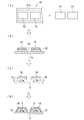
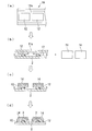
- a gas barrier film having a shape corresponding to the electronic element 3 that is the object to be sealed for example, substantially the same shape as the sealing material 12 14 is prepared. Further, the second release sheet 11b in the electronic element sealing laminated sheet 1A is peeled off. And as shown in FIG.6 (b), the said gas barrier film 14 is laminated
- the substrate 2 may be a hard material such as a glass plate, a plastic plate, or a ceramic plate, or may be a flexible material such as a resin film.
- the laminate of the sealing material 12 and the gas barrier film 14 is peeled from the first release sheet 11 a, and the laminate is contacted with the electronic element 3. Superimpose on the electronic element 3.
- This step can be performed by a known method. For example, by moving the first release sheet 11a while being bent at an acute angle in the vicinity of the electronic element 3, the laminate is released from the first release sheet 11a on the electronic element 3, and a roller or the like is removed. The laminated body is pressed to the electronic element 3 side by using, and the laminated body is superposed on the electronic element 3.
- the electronic element 3 is sealed with a laminate of the sealing material 12 and the gas barrier film 14 by heating and pressurization, vacuum lamination, or the like. Finally, the base material 2 is divided for each electronic element 3. Thereby, an electronic device in which the electronic element 3 is sealed by the sealing material 12 and the gas barrier film 14 is obtained.
- the sealing material 12 and the gas barrier film 14 have a shape corresponding to the electronic element 3, it is not necessary to remove the sealing material 12 and the gas barrier film 14 in a portion corresponding to the terminal portion of the electronic element 3, and the process is performed. It can be simplified, and there is no possibility that the terminal portion of the electronic element 3 is damaged by the removing operation, or that the sealing material 12 or the gas barrier film 14 remains on the terminal portion of the electronic element 3. Further, when the plurality of electronic elements 3 sealed on the base material 2 are divided for each electronic element 3, there is no possibility that the sealing material 12 and the gas barrier film 14 are damaged. Therefore, according to the laminated sheet 1A for encapsulating electronic elements according to this embodiment, a highly reliable electronic device can be efficiently manufactured.
- the first release sheet 11 a is peeled from the sealing material 12, and the gas barrier film 14 is laminated on the exposed sealing material 12.
- the electronic element 3 is sealed with the laminated body of the said sealing material 12 and the gas barrier film 14 by heat pressurization, a vacuum lamination, etc.
- the base material 2 is divided for each electronic element 3. Thereby, an electronic device in which the electronic element 3 is sealed by the sealing material 12 and the gas barrier film 14 is obtained. Also by this manufacturing method, a highly reliable electronic device can be manufactured efficiently similarly to the said manufacturing method.
- the first release sheet 11a is peeled off after the sealing material 12 is overlaid on the electronic element 3.
- the present invention is not limited to this, and the first release sheet 11a is peeled off.
- the sealing material 12 may be superimposed on the electronic element 3 (see the manufacturing method (5-1)).
- a gas barrier film 14 having a shape corresponding to the electronic element 3 that is the object to be encapsulated is a laminated sheet 1A for encapsulating electronic elements.
- a gas barrier film laminate sheet 4 is prepared in which a plurality of layers are laminated on a long support sheet 41 in the same arrangement as the sealing material 12 on the first release sheet 11a. Further, the second release sheet 11b in the electronic element sealing laminated sheet 1A is peeled off.
- the electronic element 3 is overlaid so as to be in contact with the electronic element 3.
- the electronic element 3 is sealed with a laminate of the sealing material 12 and the gas barrier film 14 by heating and pressurization, vacuum lamination, or the like, and the support sheet 41 is removed from the gas barrier film 14. Peel off.
- the base material 2 is divided for each electronic element 3. Thereby, an electronic device in which the electronic element 3 is sealed by the sealing material 12 and the gas barrier film 14 is obtained. Also by this manufacturing method, a highly reliable electronic device can be manufactured efficiently similarly to the said manufacturing method.
- the support sheet 41 peeled from the gas barrier film 14 after sealing it is not limited to this, You may peel from the gas barrier film 14 before sealing.
- the long gas barrier film 14 ′ is laminated on the sealing material 12 on the first release sheet 11 a in the electronic element sealing laminated sheet 1 ⁇ / b> A.
- a substrate in which a plurality of electronic elements 3 are formed on a base material 2 is prepared. Then, as shown in FIG. 9C, the first release sheet 11 a is peeled from the sealing material 12, and the sealing material 12 on the long gas barrier film 14 ′ is overlaid on the electronic element 3.
- the electronic element 3 is sealed with a laminate of the sealing material 12 and the long gas barrier film 14 ′ by heating and pressing, vacuum lamination, or the like.
- the long gas barrier film 14 ' is cut into a shape corresponding to the electronic element 3, and unnecessary portions are removed.
- the base material 2 is divided for each electronic element 3. Thereby, an electronic device in which the electronic element 3 is sealed by the sealing material 12 and the gas barrier film 14 is obtained.
- the sealing material 12 has a shape corresponding to the electronic element 3, it is not necessary to remove the sealing material 12 corresponding to the terminal portion of the electronic element 3, and the process can be simplified. There is no fear that the terminal portion of the electronic element 3 may be damaged by the removing operation, or the sealing material 12 may not remain in the terminal portion of the electronic element 3. Further, when the plurality of electronic elements 3 sealed on the base material 2 are divided for each electronic element 3, there is no possibility that the sealing material 12 is damaged. Therefore, according to the laminated sheet 1A for encapsulating electronic elements according to this embodiment, a highly reliable electronic device can be efficiently manufactured.
- an electronic element sealing laminated sheet 1 ⁇ / b> B includes a long release sheet 11 and the length of the central portion in the width direction on the release sheet 11.
- the electronic element sealing laminated sheet 1B according to the present embodiment is long, and is usually used by being unwound from a rolled-up state (see FIG. 3).
- the release sheet 11 and the sealing material 12 in the electronic element sealing laminated sheet 1B according to the present embodiment are the same as the first release sheet 11a and the sealing material 12 in the electronic element sealing laminated sheet 1A, respectively. It has a configuration.
- the gas barrier film 14 is for imparting gas barrier properties to the obtained electronic device, and for preventing or suppressing the gas from reaching the electronic element.
- the type of gas to be barrier is determined by the type of electronic device, and it is desirable to barrier water vapor in many electronic devices.
- the gas barrier film 14 has substantially the same size and shape as the sealing material 12.
- the present invention is not limited to this, and it may be any size and shape that normally exhibits gas barrier properties when the electronic element is sealed. For example, it is formed slightly larger than the sealing material 12. Also good.
- the configuration of the gas barrier film 14 is not particularly limited.
- a gas barrier layer is formed on one side or both sides of the base film directly or via other layers, and a gas barrier layer is provided in the middle of the base film. Things can be used.
- the gas barrier film 14 is preferably one in which a gas barrier layer is formed on one side or both sides of a base film directly or via another layer.
- the base film to be used is not particularly limited.
- cycloolefin resin polyethylene, polypropylene, ethylene- (meth) acrylic acid copolymer, ethylene- (meth) acrylic acid ester copolymer polyolefin, polyethylene, etc.
- Polyester such as terephthalate, polybutylene terephthalate, polyvinyl chloride, polystyrene, polyurethane, polycarbonate, polyamide, polyimide, polyamideimide, polysulfone, polyethersulfone, polyphenylene sulfide, polyarylate, acrylic resin, polybutene, polybutadiene, polymethylpentene
- a resin film made of a resin such as an ethylene vinyl acetate copolymer, an ABS resin or an ionomer resin, or a laminated film thereof.
- the base film may be a stretched film or an unstretched film. Further, the base film may contain various additives such as an ultraviolet absorber.
- the gas barrier layer may be made of any material that can suppress the permeation of gas (water vapor). Examples thereof include metals such as aluminum, magnesium, zinc, and tin, silicon nitride, silicon oxide, silicon oxynitride, and polysilazane.
- the gas barrier layer may be composed of a single layer or a plurality of layers. When the gas barrier layer is composed of a plurality of layers, each layer may be composed of different materials.
- the thickness of the gas barrier film 14 is not particularly limited, but is preferably 0.5 to 500 ⁇ m, more preferably 1 to 200 ⁇ m, and further preferably 5 to 100 ⁇ m from the viewpoint of ease of handling.
- the laminated body of the sealing material 12 and the gas barrier film 14 may be provided with two or more not only in the length direction but the width direction of the electronic element sealing laminated sheet 1B.
- the laminate of the sealing material 12 and the gas barrier film 14 has a water vapor transmission rate W (in an environment of a temperature of 40 ° C. and a relative humidity of 90% RH in terms of a thickness of 50 ⁇ m (when the thickness of the laminate is 50 ⁇ m).
- JIS K7129A method is preferably 20 g / (m 2 ⁇ day) or less, particularly preferably 15 g / (m 2 ⁇ day) or less, and more preferably 10 g / (m 2 ⁇ day) or less. It is preferable. Since the water vapor transmission rate W is within the above range, when the electronic device is sealed, water vapor from the outside is effectively blocked by the laminate and is prevented / suppressed from reaching the electronic device. The electronic device is less susceptible to moisture.
- the protective material 13 in this embodiment is formed by laminating a first protective member 13a and a second protective member 13b, but is not limited to this. It may consist of two layers, or may consist of two layers, a base material and an adhesive layer.
- the first protective member 13 a is preferably made of the same material as the sealing material 12
- the second protective member 13 b is preferably made of the same material as the gas barrier film 14.
- the protective material 13 is not an essential component, and the protective material 13 is omitted from the electronic element sealing laminated sheet 1B. Also good.
- laminated sheet 1B for encapsulating electronic element As an example of a preferred production method of laminated sheet 1B for encapsulating electronic element, first, one surface of release sheet 11 having a peelable surface (peeling) A sealing material layer made of a material constituting the sealing material 12 and a gas barrier material layer made of a material constituting the gas barrier film 14 in that order, which are approximately the same size as the release sheet 11. To be formed.
- the sealing material layer and the gas barrier material layer may be co-extruded or formed after the sealing material layer is formed by the same method as that described in the method for manufacturing the electronic element sealing laminated sheet 1A.
- a gas barrier material layer may be formed by a method, or a gas barrier material layer previously formed into a long film may be laminated.
- the gas barrier material is formed so that the laminated body of the sealing material 12 and the gas barrier film 14 having the above-described shape and the protective material 13 (laminated body of the first protective member 13a and the second protective member 13b) are formed.
- Half-cut the layer and the sealing material layer That is, only the gas barrier material layer and the sealing material layer are cut so as not to cut the release sheet 11. At this time, as long as the release sheet 11 is not cut, the release sheet 11 may be cut.
- FIG. 1A laminated sheet 1B for encapsulating electronic elements is obtained.
- the first protective member 13a is made of the same material as the sealing material 12
- the second protective member 13b is the same material as the gas barrier film 14. Consists of.
- the method for producing the electronic element sealing laminated sheet 1B is not limited to the above method.
- the sealing material 12 is sealed.
- a material constituting the gas barrier film 14 may be applied or printed on the material 12 and the first protective member 13a, or a film constituting the gas barrier film 14 may be attached.
- the protective material 13 may be formed by applying or printing a material different from the material constituting the sealing material 12 and the gas barrier film 14.
- the material constituting the sealing material 12 is applied or printed on the release surface of the release sheet 11a so that the sealing material 12 having the shape described above is formed, while the protective material 13 having the shape described above.
- a desired material may be applied or printed, or an adhesive tape may be applied so that is formed.
- an electronic element sealing laminated sheet 1B is prepared, and a sheet in which a plurality of electronic elements 3 are formed on a substrate 2 shown in FIG. 10 (b) is prepared. . Then, as shown in FIG. 10B, the laminate of the sealing material 12 and the gas barrier film 14 is peeled from the release sheet 11, and the laminate is made electronic so that the sealing material 13 contacts the electronic element 3. Superimpose on element 3.
- the electronic element 3 is sealed with a laminate of the sealing material 12 and the gas barrier film 14 by heating and pressurization, vacuum lamination, or the like. Finally, the base material 2 is divided for each electronic element 3. Thereby, an electronic device in which the electronic element 3 is sealed by the sealing material 12 and the gas barrier film 14 is obtained.
- the sealing material 12 and the gas barrier film 14 have a shape corresponding to the electronic element 3, it is not necessary to remove the sealing material 12 and the gas barrier film 14 in a portion corresponding to the terminal portion of the electronic element 3, and the process is performed. It can be simplified, and there is no possibility that the terminal portion of the electronic element 3 is damaged by the removing operation, or that the sealing material 12 or the gas barrier film 14 remains on the terminal portion of the electronic element 3. Further, when the plurality of electronic elements 3 sealed on the base material 2 are divided for each electronic element 3, there is no possibility that the sealing material 12 and the gas barrier film 14 are damaged.
- the electronic element sealing laminated sheet 1B it is not necessary to separately prepare the gas barrier film 14 or the long gas barrier film 14 'unlike the electronic element sealing laminated sheet 1A. Therefore, according to the laminated sheet 1B for encapsulating electronic elements according to this embodiment, a highly reliable electronic device can be manufactured very efficiently.
- the above laminated sheets 1A and 1B for sealing an electronic element can be applied to the manufacture of an electronic device formed by sealing an electronic element such as a display device module or a solar cell module, and the base material on which the electronic element is formed It can also be applied to a flexible electronic device using a resin film.
- the electronic element sealing laminated sheet and the electronic device manufacturing method according to the present invention are suitable for manufacturing a display device module in which an organic EL element or the like is sealed, for example.
Landscapes
- Physics & Mathematics (AREA)
- Optics & Photonics (AREA)
- Engineering & Computer Science (AREA)
- Mechanical Engineering (AREA)
- Manufacturing & Machinery (AREA)
- Electromagnetism (AREA)
- Electroluminescent Light Sources (AREA)
- Laminated Bodies (AREA)
- Packages (AREA)
- Wrappers (AREA)
Abstract
Description
ここで、本発明の実施形態では、電子素子を被封止物とする。電子素子の種類としては、封止対象となるものであれば特に限定されることなく、例えば、有機EL素子、液晶素子、発光ダイオード(LED素子)、電子ペーパー用素子、太陽電池素子等が挙げられる。また、本発明の実施形態で製造する電子デバイスは、上記のような電子素子を封止してなる電子デバイスであり、例えば、表示装置用モジュール、太陽電池モジュールなどが挙げられる。
図1および図2に示すように、本発明の第1の実施形態に係る電子素子封止用積層シート1Aは、長尺の第1の剥離シート11aと、第1の剥離シート11a上の幅方向中央部の長さ方向に、互いに異なる位置に積層された複数の封止材12と、第1の剥離シート11a上の幅方向両側部に積層された保護材13と、封止材12および保護材13の第1の剥離シート11a側とは反対側に積層された第2の長尺の剥離シート11bとを備えて構成される。なお、ここで「長尺」とは、幅に対する長さが10倍以上のことを示す。
本実施形態に係る電子素子封止用積層シート1Aにおいて、封止材12は、被封止物である電子素子に対応する形状を有する。ここで、「電子素子に対応する形状」は、電子素子を封止するのに十分な大きさを有し、かつ、封止後に封止材12の除去を必要としない形状であることが好ましい。かかる形状を有する封止材12によって電子素子を封止すれば、例えば、有機EL素子等の電子素子の端子部に対応する部分の封止材を除去する必要がなく、工程を簡略化することができるとともに、除去作業によって電子素子の端子部が損傷するおそれ、あるいは封止材が電子素子の端子部に残存するおそれがない。また、基材上にて封止された複数の電子素子を各電子素子毎に分割するときにも、封止材が損傷するおそれがない。したがって、本実施形態に係る電子素子封止用積層シート1Aによれば、信頼性の高い電子デバイスを効率良く製造することができる。
本実施形態に係る電子素子封止用積層シート1Aは、その幅方向両側部に保護材13を有する。電子素子封止用積層シート1Aがこのような保護材13を有することにより、電子素子封止用積層シート1Aをロール状に巻き取った場合でも、封止材12に印加される巻圧を低減し、封止材12に巻き痕(巻き重なった他の封止材12の輪郭の痕)やシワができることを抑制することができる。
第1の剥離シート11aおよび第2の剥離シート11bとしては、封止材12を支持することができ、かつ封止材12から容易に剥離することができるものであれば、特に限定されることはない。
電子素子封止用積層シート1Aの好ましい製造方法の一例としては、最初に、第1の剥離シート11aの一方の表面であって、剥離性を有する面(剥離面)に、当該第1の剥離シート11aと略同じ大きさで、封止材12を構成する材料からなる封止材料層を形成する。
電子素子封止用積層シート1Aを使用して電子デバイスを製造する方法としては、種々の方法が挙げられ、例えば、以下の方法を例示することができる。
図6(a)に示すように、電子素子封止用積層シート1Aの他に、被封止物である電子素子3に対応する形状、例えば封止材12とほぼ同一の形状を有するガスバリアフィルム14を用意する。また、電子素子封止用積層シート1Aにおける第2の剥離シート11bを剥離する。そして、図6(b)に示すように、封止材12の第1の剥離シート11a側とは反対側に、上記ガスバリアフィルム14を積層する。
図7(a)に示すように、電子素子封止用積層シート1Aにおける第2の剥離シート11bを剥離する。そして、図7(b)に示すように、基材2上に複数の電子素子3が形成されたものを用意し、第1の剥離シート11aに積層された封止材12を、その状態で電子素子3に重ね合わせる。一方、被封止物である電子素子3に対応する形状を有するガスバリアフィルム14を用意する。
図8(a)に示すように、電子素子封止用積層シート1Aの他に、被封止物である電子素子3に対応する形状を有するガスバリアフィルム14が、電子素子封止用積層シート1Aにおける第1の剥離シート11a上の封止材12と同じ配列にて、長尺の支持シート41上に複数積層されてなるガスバリアフィルム積層シート4を用意する。また、電子素子封止用積層シート1Aにおける第2の剥離シート11bを剥離する。
図9(a)に示すように、電子素子封止用積層シート1Aの他に、長尺のガスバリアフィルム14’を用意する。また、電子素子封止用積層シート1Aにおける第2の剥離シート11bを剥離する。
図3および図4に示すように、本発明の第2の実施形態に係る電子素子封止用積層シート1Bは、長尺の剥離シート11と、剥離シート11上の幅方向中央部の長さ方向に、互いに異なる位置に積層された複数の封止材12と、封止材12の剥離シート11側とは反対側に積層されたガスバリアフィルム14と、剥離シート11上の幅方向両側部に積層された保護材13とを備えて構成される。
ガスバリアフィルム14は、得られる電子デバイスにガスバリア性を付与し、電子素子にガスが到達することを防止・抑制するためのものである。バリアすべきガスの種類は、電子素子の種類によって決定され、多くの電子素子では水蒸気をバリアすることが望ましい。
本実施形態における保護材13は、一例として、第1の保護部材13aと第2の保護部材13bとを積層してなるが、これに限定されるものではなく、例えば、単層からなってもよいし、基材および粘着剤層の2層からなってもよい。本実施形態において、第1の保護部材13aは、封止材12と同じ材料からなることが好ましく、第2の保護部材13bは、ガスバリアフィルム14と同じ材料からなることが好ましい。これにより、後述する方法により、電子素子封止用積層シート1Bを簡易に製造することができる。
電子素子封止用積層シート1Bの好ましい製造方法の一例としては、最初に、剥離シート11の一方の表面であって、剥離性を有する面(剥離面)に、当該剥離シート11と略同じ大きさで、封止材12を構成する材料からなる封止材料層と、ガスバリアフィルム14を構成する材料からなるガスバリア材料層とを、その順で積層されるように形成する。
電子素子封止用積層シート1Bを使用して電子デバイスを製造する方法としては、例えば、以下の方法を例示することができる。
11…剥離シート
11a…第1の剥離シート
11b…第2の剥離シート
12…封止材
13…保護材
13a…第1の保護部材
13b…第2の保護部材
14…ガスバリアフィルム
14’…長尺のガスバリアフィルム
2…基材
3…電子素子
4…ガスバリアフィルム積層シート
41…支持シート
Claims (21)
- 長尺の剥離シートと、
前記長尺の剥離シート上、互いに異なる位置に複数積層された、被封止物である電子素子に対応する形状を有する封止材と
を備えたことを特徴とする電子素子封止用積層シート。 - 前記長尺の剥離シートの幅方向両側部には、保護材が設けられており、
前記封止材は、前記長尺の剥離シート上、前記保護材とは異なる位置に設けられている
ことを特徴とする請求項1に記載の電子素子封止用積層シート。 - 前記保護材の厚さは、前記封止材の厚さと同等か、前記封止材よりも厚いことを特徴とする請求項2に記載の電子素子封止用積層シート。
- 前記保護材は、前記封止材と同じ材料から構成されていることを特徴とする請求項2に記載の電子素子封止用積層シート。
- 前記封止材の前記剥離シート側とは反対側には、被封止物である電子素子に対応する形状を有するガスバリアフィルムが積層されていることを特徴とする請求項1に記載の電子素子封止用積層シート。
- 前記長尺の剥離シートの幅方向両側部には、保護材が設けられており、
前記封止材および前記ガスバリアフィルムの積層体は、前記長尺の剥離シート上、前記保護材とは異なる位置に設けられている
ことを特徴とする請求項5に記載の電子素子封止用積層シート。 - 前記保護材の厚さは、前記封止材および前記ガスバリアフィルムの積層体の厚さと同等か、前記積層体よりも厚いことを特徴とする請求項6に記載の電子素子封止用積層シート。
- 前記保護材は、前記封止材および前記ガスバリアフィルムの積層体と同じ材料から構成されていることを特徴とする請求項6に記載の電子素子封止用積層シート。
- 前記封止材の前記剥離シート側とは反対側には、第2の長尺の剥離シートが積層されていることを特徴とする請求項1に記載の電子素子封止用積層シート。
- 前記封止材は、前記長尺の剥離シートの少なくとも長さ方向に複数設けられていることを特徴とする請求項1に記載の電子素子封止用積層シート。
- 前記封止材は、前記長尺の剥離シートの幅方向にも複数設けられていることを特徴とする請求項10に記載の電子素子封止用積層シート。
- 被封止物である前記電子素子は、有機EL素子であることを特徴とする請求項1に記載の電子素子封止用積層シート。
- 前記封止材は、酸変性ポリオレフィン系樹脂、シラン変性ポリオレフィン系樹脂、アイオノマー、エチレン-(メタ)アクリル酸共重合体およびゴム系樹脂からなる群から選ばれる少なくとも一種から構成されることを特徴とする請求項1に記載の電子素子封止用積層シート。
- 前記封止材および前記ガスバリアフィルムの積層体は、厚み50μm換算の、温度40℃、相対湿度90%RHの環境下における水蒸気透過率が、20g/(m2・day)以下であることを特徴とする請求項1に記載の電子素子封止用積層シート。
- 請求項4に記載の電子素子封止用積層シートの製造方法であって、
前記長尺の剥離シートの一方の面に、前記剥離シートと略同じ大きさで、前記封止材を構成する材料からなる封止材料層を形成し、
前記封止材および前記保護材が形成されるように、前記封止材料層をハーフカットし、余分な部分を除去する
ことを特徴とする電子素子封止用積層シートの製造方法。 - 請求項8に記載の電子素子封止用積層シートの製造方法であって、
前記長尺の剥離シートの一方の面に、前記剥離シートと略同じ大きさで、前記封止材を構成する材料からなる封止材料層と、前記ガスバリアフィルムを構成する材料からなるガスバリア材料層とを、その順で積層されるように形成し、
前記封止材および前記ガスバリアフィルムの積層体、ならびに前記保護材が形成されるように、前記ガスバリア材料層および封止材料層をハーフカットし、余分な部分を除去する
ことを特徴とする電子素子封止用積層シートの製造方法。 - 請求項1~4のいずれか一項に記載の電子素子封止用積層シートにおける前記封止材の前記剥離シート側とは反対側に、被封止物である電子素子に対応する形状を有するガスバリアフィルムを積層し、
前記封止材および前記ガスバリアフィルムの積層体を、前記剥離シートから剥離し、
前記封止材および前記ガスバリアフィルムの積層体を、前記封止材が被封止物である電子素子に接触するように、前記電子素子に重ね合わせ、前記電子素子を封止する
ことを特徴とする電子デバイスの製造方法。 - 請求項1~4のいずれか一項に記載の電子素子封止用積層シートにおける前記封止材を、被封止物である電子素子に重ね合わせ、
任意の段階で前記封止材から前記剥離シートを剥離し、
前記封止材の前記電子素子側とは反対側に、被封止物である電子素子に対応する形状を有するガスバリアフィルムを積層し、
前記電子素子を封止する
ことを特徴とする電子デバイスの製造方法。 - 被封止物である電子素子に対応する形状を有するガスバリアフィルムが、請求項1~4のいずれか一項に記載の電子素子封止用積層シートにおける前記長尺の剥離シート上の前記封止材と同じ配列にて、長尺の支持シート上に複数積層されてなるガスバリアフィルム積層シートを用意し、
前記電子素子封止用積層シートにおける前記長尺の剥離シート上の前記封止材と、前記ガスバリアフィルム積層シートにおける前記長尺の支持シート上の前記ガスバリアフィルムとを積層し、
前記封止材から前記剥離シートを剥離し、
前記支持シート上の前記ガスバリアフィルムおよび前記封止材の積層体を、前記封止材が被封止物である電子素子に接触するように、前記電子素子に重ね合わせ、前記電子素子を封止し、
任意の段階で前記ガスバリアフィルムから前記支持シートを剥離する
ことを特徴とする電子デバイスの製造方法。 - 請求項1~4のいずれか一項に記載の電子素子封止用積層シートにおける前記封止材の前記剥離シート側とは反対側に、長尺のガスバリアフィルムを積層し、
前記封止材から前記剥離シートを剥離し、
前記長尺のガスバリアフィルム上の前記封止材を前記電子素子に重ね合わせ、前記電子素子を封止し、
前記長尺のガスバリアフィルムを前記電子素子に対応する形状にカットし、不要部分を除去する
ことを特徴とする電子デバイスの製造方法。 - 請求項5~8のいずれか一項に記載の電子素子封止用積層シートにおける前記封止材および前記ガスバリアフィルムの積層体を前記剥離シートから剥離し、
前記封止材および前記ガスバリアフィルムの積層体を、前記封止材が被封止物である電子素子に接触するように、前記電子素子に重ね合わせ、前記電子素子を封止する
ことを特徴とする電子デバイスの製造方法。
Priority Applications (5)
| Application Number | Priority Date | Filing Date | Title |
|---|---|---|---|
| JP2016508667A JP6501755B2 (ja) | 2014-03-19 | 2015-03-09 | 電子素子封止用積層シートおよび電子デバイスの製造方法 |
| EP15765170.4A EP3122156A4 (en) | 2014-03-19 | 2015-03-09 | Laminated sheet for sealing electronic elements and production method for electronic device |
| US15/124,711 US20170025636A1 (en) | 2014-03-19 | 2015-03-09 | Laminated sheet for sealing electronic elements and production method for electronic devices |
| CN201580014511.1A CN106134288B (zh) | 2014-03-19 | 2015-03-09 | 电子元件封装用层叠片以及电子器件的制造方法 |
| KR1020167024628A KR102278124B1 (ko) | 2014-03-19 | 2015-03-09 | 전자 소자 밀봉용 적층 시트 및 전자 디바이스의 제조 방법 |
Applications Claiming Priority (2)
| Application Number | Priority Date | Filing Date | Title |
|---|---|---|---|
| JP2014-057143 | 2014-03-19 | ||
| JP2014057143 | 2014-03-19 |
Publications (1)
| Publication Number | Publication Date |
|---|---|
| WO2015141512A1 true WO2015141512A1 (ja) | 2015-09-24 |
Family
ID=54144483
Family Applications (1)
| Application Number | Title | Priority Date | Filing Date |
|---|---|---|---|
| PCT/JP2015/056881 Ceased WO2015141512A1 (ja) | 2014-03-19 | 2015-03-09 | 電子素子封止用積層シートおよび電子デバイスの製造方法 |
Country Status (7)
| Country | Link |
|---|---|
| US (1) | US20170025636A1 (ja) |
| EP (1) | EP3122156A4 (ja) |
| JP (1) | JP6501755B2 (ja) |
| KR (1) | KR102278124B1 (ja) |
| CN (1) | CN106134288B (ja) |
| TW (1) | TWI655797B (ja) |
| WO (1) | WO2015141512A1 (ja) |
Cited By (2)
| Publication number | Priority date | Publication date | Assignee | Title |
|---|---|---|---|---|
| JP2018067383A (ja) * | 2016-10-17 | 2018-04-26 | 株式会社ジャパンディスプレイ | 表示装置 |
| WO2018072297A1 (zh) * | 2016-10-19 | 2018-04-26 | 深圳市华星光电技术有限公司 | Oled显示面板的制作方法 |
Families Citing this family (9)
| Publication number | Priority date | Publication date | Assignee | Title |
|---|---|---|---|---|
| KR102597464B1 (ko) * | 2016-06-10 | 2023-11-06 | 삼성디스플레이 주식회사 | 표시 장치 및 이의 제조 방법 |
| CN110709485B (zh) * | 2017-05-31 | 2022-06-28 | 琳得科株式会社 | 片状粘接剂、阻气层叠体及密封体 |
| CN111629892A (zh) * | 2018-01-24 | 2020-09-04 | 琳得科株式会社 | 长条层叠片的卷料 |
| WO2019146605A1 (ja) * | 2018-01-24 | 2019-08-01 | リンテック株式会社 | 長尺積層シートおよびその巻収体 |
| US20210195693A1 (en) * | 2018-05-30 | 2021-06-24 | Lintec Corporation | Heat-generating sheet |
| WO2020205917A1 (en) * | 2019-04-01 | 2020-10-08 | First Solar, Inc. | Photovoltaic devices with encapsulation layers and systems and methods for forming the same |
| CN114822246A (zh) * | 2022-04-02 | 2022-07-29 | 昆山国显光电有限公司 | 一种支撑模组 |
| TWI823757B (zh) * | 2023-01-18 | 2023-11-21 | 友達光電股份有限公司 | 顯示裝置 |
| CN116100656B (zh) * | 2023-03-28 | 2023-07-25 | 铜陵优必胜新材料科技有限公司 | 一种陶瓷片覆膜定型装置、生产线及定型方法 |
Citations (4)
| Publication number | Priority date | Publication date | Assignee | Title |
|---|---|---|---|---|
| JPS5852896U (ja) * | 1981-09-25 | 1983-04-09 | 日本電気ホームエレクトロニクス株式会社 | 電界発光灯の封止構体 |
| JP2004303528A (ja) * | 2003-03-31 | 2004-10-28 | Toppan Printing Co Ltd | 有機エレクトロルミネッセンス素子及びその製造方法 |
| JP2012089339A (ja) * | 2010-10-19 | 2012-05-10 | Lintec Corp | 封止用治具及びデバイス封止方法 |
| JP2014500586A (ja) * | 2010-11-02 | 2014-01-09 | エルジー・ケム・リミテッド | 接着フィルム及びこれを利用した有機電子装置の封止方法 |
Family Cites Families (7)
| Publication number | Priority date | Publication date | Assignee | Title |
|---|---|---|---|---|
| US6867539B1 (en) * | 2000-07-12 | 2005-03-15 | 3M Innovative Properties Company | Encapsulated organic electronic devices and method for making same |
| JP4419012B2 (ja) | 2002-09-27 | 2010-02-24 | 株式会社スリーボンド | 有機el素子用封止材及び有機el素子の封止方法 |
| JP3921482B2 (ja) | 2004-07-28 | 2007-05-30 | トッキ株式会社 | 有機el素子の製造装置並びに有機el素子 |
| US7834543B2 (en) * | 2007-07-03 | 2010-11-16 | Canon Kabushiki Kaisha | Organic EL display apparatus and method of manufacturing the same |
| JP5326098B2 (ja) * | 2009-02-05 | 2013-10-30 | シャープ株式会社 | 基板表面の封止装置と有機elパネルの製造方法 |
| EP2448032B1 (en) * | 2009-06-24 | 2014-09-17 | Mitsubishi Chemical Corporation | Organic electronic device and method for producing the same |
| KR20120079319A (ko) * | 2011-01-04 | 2012-07-12 | 삼성모바일디스플레이주식회사 | 평판 디스플레이 장치 및 유기 발광 디스플레이 장치 |
-
2015
- 2015-03-09 CN CN201580014511.1A patent/CN106134288B/zh active Active
- 2015-03-09 JP JP2016508667A patent/JP6501755B2/ja active Active
- 2015-03-09 EP EP15765170.4A patent/EP3122156A4/en not_active Withdrawn
- 2015-03-09 KR KR1020167024628A patent/KR102278124B1/ko active Active
- 2015-03-09 US US15/124,711 patent/US20170025636A1/en not_active Abandoned
- 2015-03-09 WO PCT/JP2015/056881 patent/WO2015141512A1/ja not_active Ceased
- 2015-03-13 TW TW104108036A patent/TWI655797B/zh active
Patent Citations (4)
| Publication number | Priority date | Publication date | Assignee | Title |
|---|---|---|---|---|
| JPS5852896U (ja) * | 1981-09-25 | 1983-04-09 | 日本電気ホームエレクトロニクス株式会社 | 電界発光灯の封止構体 |
| JP2004303528A (ja) * | 2003-03-31 | 2004-10-28 | Toppan Printing Co Ltd | 有機エレクトロルミネッセンス素子及びその製造方法 |
| JP2012089339A (ja) * | 2010-10-19 | 2012-05-10 | Lintec Corp | 封止用治具及びデバイス封止方法 |
| JP2014500586A (ja) * | 2010-11-02 | 2014-01-09 | エルジー・ケム・リミテッド | 接着フィルム及びこれを利用した有機電子装置の封止方法 |
Non-Patent Citations (1)
| Title |
|---|
| See also references of EP3122156A4 * |
Cited By (2)
| Publication number | Priority date | Publication date | Assignee | Title |
|---|---|---|---|---|
| JP2018067383A (ja) * | 2016-10-17 | 2018-04-26 | 株式会社ジャパンディスプレイ | 表示装置 |
| WO2018072297A1 (zh) * | 2016-10-19 | 2018-04-26 | 深圳市华星光电技术有限公司 | Oled显示面板的制作方法 |
Also Published As
| Publication number | Publication date |
|---|---|
| KR20160135717A (ko) | 2016-11-28 |
| JPWO2015141512A1 (ja) | 2017-04-06 |
| EP3122156A1 (en) | 2017-01-25 |
| CN106134288A (zh) | 2016-11-16 |
| CN106134288B (zh) | 2018-01-02 |
| US20170025636A1 (en) | 2017-01-26 |
| KR102278124B1 (ko) | 2021-07-15 |
| TW201539824A (zh) | 2015-10-16 |
| EP3122156A4 (en) | 2017-11-29 |
| TWI655797B (zh) | 2019-04-01 |
| JP6501755B2 (ja) | 2019-04-17 |
Similar Documents
| Publication | Publication Date | Title |
|---|---|---|
| JP6501755B2 (ja) | 電子素子封止用積層シートおよび電子デバイスの製造方法 | |
| CN103374308B (zh) | 透明导电性膜用表面保护膜以及使用其的透明导电性膜 | |
| JP5573678B2 (ja) | 有機エレクトロルミネッセンス素子の製造方法、有機エレクトロルミネッセンス素子 | |
| JP2019137832A (ja) | 粘着シートおよび粘着シート積層体 | |
| TW200845454A (en) | Method of encapsulating an environmentally sensitive device | |
| JP5997043B2 (ja) | フィルム状封止材、封止シートおよび電子デバイス | |
| CN1973011A (zh) | 粘合片材和剥离材料 | |
| KR101418196B1 (ko) | 봉지된 기능 소자 | |
| JP6461189B2 (ja) | 封止シート、電子デバイス用部材および電子デバイス | |
| CN104718797A (zh) | 有机电致发光装置的制造方法 | |
| JP6064502B2 (ja) | 積層体製造方法、積層体製造装置および積層体 | |
| CN101959984A (zh) | 粘着片及使用该粘着片的带剥离片粘着片 | |
| JP2015114654A (ja) | ラベル及びラベル付き物品 | |
| JP2008260540A (ja) | シート状光学フィルム包装体 | |
| JP2008311513A (ja) | 表面保護用シートの支持構造および半導体ウエハの研削方法 | |
| CN104669734A (zh) | 一种具有多层使用层的保护膜及其制备方法 | |
| JP2008311152A (ja) | 電子機器積層体 | |
| JP2021064745A (ja) | 封止用フィルム、封止用フィルム被覆電子部品搭載基板および電子機器 | |
| KR102186008B1 (ko) | 물탱크 시일링용 일면 접합형 접합 테이프, 그 제조 방법 및 이를 이용한 물탱크 모듈 | |
| CN204824701U (zh) | 一种紫外光固化剥离压敏胶带 | |
| WO2016059932A1 (ja) | 易貼付粘着テープ又はシート | |
| WO2013164890A1 (ja) | グラフェン積層体 | |
| JP2013256089A (ja) | 表面保護部材およびその製造方法 | |
| JP2008150613A (ja) | 積層シートおよびその製造方法 | |
| JP2008081190A (ja) | 光学シート用の包装材、光学シート包装体、及び包装材封止用粘着テープ |
Legal Events
| Date | Code | Title | Description |
|---|---|---|---|
| 121 | Ep: the epo has been informed by wipo that ep was designated in this application |
Ref document number: 15765170 Country of ref document: EP Kind code of ref document: A1 |
|
| ENP | Entry into the national phase |
Ref document number: 2016508667 Country of ref document: JP Kind code of ref document: A |
|
| ENP | Entry into the national phase |
Ref document number: 20167024628 Country of ref document: KR Kind code of ref document: A |
|
| WWE | Wipo information: entry into national phase |
Ref document number: 15124711 Country of ref document: US |
|
| NENP | Non-entry into the national phase |
Ref country code: DE |
|
| REEP | Request for entry into the european phase |
Ref document number: 2015765170 Country of ref document: EP |
|
| WWE | Wipo information: entry into national phase |
Ref document number: 2015765170 Country of ref document: EP |