WO2015146926A1 - 半導体素子及び絶縁層形成用組成物 - Google Patents
半導体素子及び絶縁層形成用組成物 Download PDFInfo
- Publication number
- WO2015146926A1 WO2015146926A1 PCT/JP2015/058775 JP2015058775W WO2015146926A1 WO 2015146926 A1 WO2015146926 A1 WO 2015146926A1 JP 2015058775 W JP2015058775 W JP 2015058775W WO 2015146926 A1 WO2015146926 A1 WO 2015146926A1
- Authority
- WO
- WIPO (PCT)
- Prior art keywords
- group
- general formula
- represented
- repeating unit
- compound
- Prior art date
- Legal status (The legal status is an assumption and is not a legal conclusion. Google has not performed a legal analysis and makes no representation as to the accuracy of the status listed.)
- Ceased
Links
- 0 *C(*)(CC(C(*)(*)N)C=*)N Chemical compound *C(*)(CC(C(*)(*)N)C=*)N 0.000 description 61
- QTTJMBRHORIMHZ-UHFFFAOYSA-N Bc(c1c2c([Br]=C)ccc1C)ccc2NCCCC=C Chemical compound Bc(c1c2c([Br]=C)ccc1C)ccc2NCCCC=C QTTJMBRHORIMHZ-UHFFFAOYSA-N 0.000 description 1
- JUIJOCSLABMQEX-UHFFFAOYSA-N CC(CC1OC1C1)C1O Chemical compound CC(CC1OC1C1)C1O JUIJOCSLABMQEX-UHFFFAOYSA-N 0.000 description 1
- ZTDNIXJNCIJIOR-UHFFFAOYSA-N CC1C=C(COC)C(OCCOc2ccc(C)cc2)=C(COC)C1 Chemical compound CC1C=C(COC)C(OCCOc2ccc(C)cc2)=C(COC)C1 ZTDNIXJNCIJIOR-UHFFFAOYSA-N 0.000 description 1
- ZAAZLPLQBVGPST-UHFFFAOYSA-N CCCCC1=Nc(c2c34)ccc3SC(CCCC)=Nc4ccc2S1 Chemical compound CCCCC1=Nc(c2c34)ccc3SC(CCCC)=Nc4ccc2S1 ZAAZLPLQBVGPST-UHFFFAOYSA-N 0.000 description 1
- NJTFSNBKMMZUCQ-UHFFFAOYSA-N CCCOc1c(C)cc(COC)cc1C Chemical compound CCCOc1c(C)cc(COC)cc1C NJTFSNBKMMZUCQ-UHFFFAOYSA-N 0.000 description 1
- KQSABULTKYLFEV-UHFFFAOYSA-N Nc1cccc2c1cccc2N Chemical compound Nc1cccc2c1cccc2N KQSABULTKYLFEV-UHFFFAOYSA-N 0.000 description 1
- YRFZSARRGPTTDT-UHFFFAOYSA-N O=S(C(CC1)CC2C1C1OC1CC2)=O Chemical compound O=S(C(CC1)CC2C1C1OC1CC2)=O YRFZSARRGPTTDT-UHFFFAOYSA-N 0.000 description 1
- AEKLVVBOABEASC-UHFFFAOYSA-O O[SH+](C(CC1)C(CC2)C1C(CC1)C2C2C1CC1OC1C2)=O Chemical compound O[SH+](C(CC1)C(CC2)C1C(CC1)C2C2C1CC1OC1C2)=O AEKLVVBOABEASC-UHFFFAOYSA-O 0.000 description 1
Images

Classifications
-
- C—CHEMISTRY; METALLURGY
- C08—ORGANIC MACROMOLECULAR COMPOUNDS; THEIR PREPARATION OR CHEMICAL WORKING-UP; COMPOSITIONS BASED THEREON
- C08F—MACROMOLECULAR COMPOUNDS OBTAINED BY REACTIONS ONLY INVOLVING CARBON-TO-CARBON UNSATURATED BONDS
- C08F212/00—Copolymers of compounds having one or more unsaturated aliphatic radicals, each having only one carbon-to-carbon double bond, and at least one being terminated by an aromatic carbocyclic ring
- C08F212/02—Monomers containing only one unsaturated aliphatic radical
- C08F212/04—Monomers containing only one unsaturated aliphatic radical containing one ring
- C08F212/14—Monomers containing only one unsaturated aliphatic radical containing one ring substituted by heteroatoms or groups containing heteroatoms
- C08F212/22—Oxygen
- C08F212/24—Phenols or alcohols
-
- C—CHEMISTRY; METALLURGY
- C08—ORGANIC MACROMOLECULAR COMPOUNDS; THEIR PREPARATION OR CHEMICAL WORKING-UP; COMPOSITIONS BASED THEREON
- C08F—MACROMOLECULAR COMPOUNDS OBTAINED BY REACTIONS ONLY INVOLVING CARBON-TO-CARBON UNSATURATED BONDS
- C08F12/00—Homopolymers and copolymers of compounds having one or more unsaturated aliphatic radicals, each having only one carbon-to-carbon double bond, and at least one being terminated by an aromatic carbocyclic ring
- C08F12/02—Monomers containing only one unsaturated aliphatic radical
- C08F12/04—Monomers containing only one unsaturated aliphatic radical containing one ring
- C08F12/14—Monomers containing only one unsaturated aliphatic radical containing one ring substituted by hetero atoms or groups containing heteroatoms
- C08F12/22—Oxygen
-
- C—CHEMISTRY; METALLURGY
- C08—ORGANIC MACROMOLECULAR COMPOUNDS; THEIR PREPARATION OR CHEMICAL WORKING-UP; COMPOSITIONS BASED THEREON
- C08F—MACROMOLECULAR COMPOUNDS OBTAINED BY REACTIONS ONLY INVOLVING CARBON-TO-CARBON UNSATURATED BONDS
- C08F12/00—Homopolymers and copolymers of compounds having one or more unsaturated aliphatic radicals, each having only one carbon-to-carbon double bond, and at least one being terminated by an aromatic carbocyclic ring
- C08F12/02—Monomers containing only one unsaturated aliphatic radical
- C08F12/04—Monomers containing only one unsaturated aliphatic radical containing one ring
- C08F12/14—Monomers containing only one unsaturated aliphatic radical containing one ring substituted by hetero atoms or groups containing heteroatoms
- C08F12/22—Oxygen
- C08F12/24—Phenols or alcohols
-
- C—CHEMISTRY; METALLURGY
- C08—ORGANIC MACROMOLECULAR COMPOUNDS; THEIR PREPARATION OR CHEMICAL WORKING-UP; COMPOSITIONS BASED THEREON
- C08F—MACROMOLECULAR COMPOUNDS OBTAINED BY REACTIONS ONLY INVOLVING CARBON-TO-CARBON UNSATURATED BONDS
- C08F20/00—Homopolymers and copolymers of compounds having one or more unsaturated aliphatic radicals, each having only one carbon-to-carbon double bond, and only one being terminated by only one carboxyl radical or a salt, anhydride, ester, amide, imide or nitrile thereof
- C08F20/02—Monocarboxylic acids having less than ten carbon atoms, Derivatives thereof
- C08F20/10—Esters
- C08F20/26—Esters containing oxygen in addition to the carboxy oxygen
- C08F20/28—Esters containing oxygen in addition to the carboxy oxygen containing no aromatic rings in the alcohol moiety
-
- C—CHEMISTRY; METALLURGY
- C08—ORGANIC MACROMOLECULAR COMPOUNDS; THEIR PREPARATION OR CHEMICAL WORKING-UP; COMPOSITIONS BASED THEREON
- C08F—MACROMOLECULAR COMPOUNDS OBTAINED BY REACTIONS ONLY INVOLVING CARBON-TO-CARBON UNSATURATED BONDS
- C08F212/00—Copolymers of compounds having one or more unsaturated aliphatic radicals, each having only one carbon-to-carbon double bond, and at least one being terminated by an aromatic carbocyclic ring
- C08F212/02—Monomers containing only one unsaturated aliphatic radical
- C08F212/04—Monomers containing only one unsaturated aliphatic radical containing one ring
- C08F212/14—Monomers containing only one unsaturated aliphatic radical containing one ring substituted by heteroatoms or groups containing heteroatoms
- C08F212/22—Oxygen
-
- H—ELECTRICITY
- H10—SEMICONDUCTOR DEVICES; ELECTRIC SOLID-STATE DEVICES NOT OTHERWISE PROVIDED FOR
- H10D—INORGANIC ELECTRIC SEMICONDUCTOR DEVICES
- H10D30/00—Field-effect transistors [FET]
- H10D30/60—Insulated-gate field-effect transistors [IGFET]
- H10D30/67—Thin-film transistors [TFT]
-
- H—ELECTRICITY
- H10—SEMICONDUCTOR DEVICES; ELECTRIC SOLID-STATE DEVICES NOT OTHERWISE PROVIDED FOR
- H10K—ORGANIC ELECTRIC SOLID-STATE DEVICES
- H10K10/00—Organic devices specially adapted for rectifying, amplifying, oscillating or switching; Organic capacitors or resistors having potential barriers
- H10K10/40—Organic transistors
- H10K10/46—Field-effect transistors, e.g. organic thin-film transistors [OTFT]
- H10K10/462—Insulated gate field-effect transistors [IGFETs]
- H10K10/466—Lateral bottom-gate IGFETs comprising only a single gate
-
- H—ELECTRICITY
- H10—SEMICONDUCTOR DEVICES; ELECTRIC SOLID-STATE DEVICES NOT OTHERWISE PROVIDED FOR
- H10K—ORGANIC ELECTRIC SOLID-STATE DEVICES
- H10K10/00—Organic devices specially adapted for rectifying, amplifying, oscillating or switching; Organic capacitors or resistors having potential barriers
- H10K10/40—Organic transistors
- H10K10/46—Field-effect transistors, e.g. organic thin-film transistors [OTFT]
- H10K10/462—Insulated gate field-effect transistors [IGFETs]
- H10K10/468—Insulated gate field-effect transistors [IGFETs] characterised by the gate dielectrics
- H10K10/471—Insulated gate field-effect transistors [IGFETs] characterised by the gate dielectrics the gate dielectric comprising only organic materials
-
- H—ELECTRICITY
- H10—SEMICONDUCTOR DEVICES; ELECTRIC SOLID-STATE DEVICES NOT OTHERWISE PROVIDED FOR
- H10K—ORGANIC ELECTRIC SOLID-STATE DEVICES
- H10K10/00—Organic devices specially adapted for rectifying, amplifying, oscillating or switching; Organic capacitors or resistors having potential barriers
- H10K10/40—Organic transistors
- H10K10/46—Field-effect transistors, e.g. organic thin-film transistors [OTFT]
- H10K10/462—Insulated gate field-effect transistors [IGFETs]
- H10K10/484—Insulated gate field-effect transistors [IGFETs] characterised by the channel regions
- H10K10/488—Insulated gate field-effect transistors [IGFETs] characterised by the channel regions the channel region comprising a layer of composite material having interpenetrating or embedded materials, e.g. a mixture of donor and acceptor moieties, that form a bulk heterojunction
-
- H—ELECTRICITY
- H10—SEMICONDUCTOR DEVICES; ELECTRIC SOLID-STATE DEVICES NOT OTHERWISE PROVIDED FOR
- H10K—ORGANIC ELECTRIC SOLID-STATE DEVICES
- H10K85/00—Organic materials used in the body or electrodes of devices covered by this subclass
- H10K85/10—Organic polymers or oligomers
- H10K85/141—Organic polymers or oligomers comprising aliphatic or olefinic chains, e.g. poly N-vinylcarbazol, PVC or PTFE
-
- H—ELECTRICITY
- H10—SEMICONDUCTOR DEVICES; ELECTRIC SOLID-STATE DEVICES NOT OTHERWISE PROVIDED FOR
- H10K—ORGANIC ELECTRIC SOLID-STATE DEVICES
- H10K85/00—Organic materials used in the body or electrodes of devices covered by this subclass
- H10K85/10—Organic polymers or oligomers
- H10K85/151—Copolymers
-
- H—ELECTRICITY
- H10—SEMICONDUCTOR DEVICES; ELECTRIC SOLID-STATE DEVICES NOT OTHERWISE PROVIDED FOR
- H10K—ORGANIC ELECTRIC SOLID-STATE DEVICES
- H10K85/00—Organic materials used in the body or electrodes of devices covered by this subclass
- H10K85/40—Organosilicon compounds, e.g. TIPS pentacene
-
- H—ELECTRICITY
- H10—SEMICONDUCTOR DEVICES; ELECTRIC SOLID-STATE DEVICES NOT OTHERWISE PROVIDED FOR
- H10K—ORGANIC ELECTRIC SOLID-STATE DEVICES
- H10K85/00—Organic materials used in the body or electrodes of devices covered by this subclass
- H10K85/60—Organic compounds having low molecular weight
- H10K85/615—Polycyclic condensed aromatic hydrocarbons, e.g. anthracene
- H10K85/623—Polycyclic condensed aromatic hydrocarbons, e.g. anthracene containing five rings, e.g. pentacene
-
- H—ELECTRICITY
- H10—SEMICONDUCTOR DEVICES; ELECTRIC SOLID-STATE DEVICES NOT OTHERWISE PROVIDED FOR
- H10K—ORGANIC ELECTRIC SOLID-STATE DEVICES
- H10K85/00—Organic materials used in the body or electrodes of devices covered by this subclass
- H10K85/60—Organic compounds having low molecular weight
- H10K85/649—Aromatic compounds comprising a hetero atom
- H10K85/657—Polycyclic condensed heteroaromatic hydrocarbons
-
- H—ELECTRICITY
- H10—SEMICONDUCTOR DEVICES; ELECTRIC SOLID-STATE DEVICES NOT OTHERWISE PROVIDED FOR
- H10P—GENERIC PROCESSES OR APPARATUS FOR THE MANUFACTURE OR TREATMENT OF DEVICES COVERED BY CLASS H10
- H10P14/00—Formation of materials, e.g. in the shape of layers or pillars
- H10P14/60—Formation of materials, e.g. in the shape of layers or pillars of insulating materials
- H10P14/68—Organic materials, e.g. photoresists
- H10P14/683—Organic materials, e.g. photoresists carbon-based polymeric organic materials, e.g. polyimides, poly cyclobutene or PVC
-
- C—CHEMISTRY; METALLURGY
- C08—ORGANIC MACROMOLECULAR COMPOUNDS; THEIR PREPARATION OR CHEMICAL WORKING-UP; COMPOSITIONS BASED THEREON
- C08F—MACROMOLECULAR COMPOUNDS OBTAINED BY REACTIONS ONLY INVOLVING CARBON-TO-CARBON UNSATURATED BONDS
- C08F2500/00—Characteristics or properties of obtained polyolefins; Use thereof
- C08F2500/02—Low molecular weight, e.g. <100,000 Da.
-
- C—CHEMISTRY; METALLURGY
- C08—ORGANIC MACROMOLECULAR COMPOUNDS; THEIR PREPARATION OR CHEMICAL WORKING-UP; COMPOSITIONS BASED THEREON
- C08F—MACROMOLECULAR COMPOUNDS OBTAINED BY REACTIONS ONLY INVOLVING CARBON-TO-CARBON UNSATURATED BONDS
- C08F2800/00—Copolymer characterised by the proportions of the comonomers expressed
- C08F2800/10—Copolymer characterised by the proportions of the comonomers expressed as molar percentages
-
- C—CHEMISTRY; METALLURGY
- C08—ORGANIC MACROMOLECULAR COMPOUNDS; THEIR PREPARATION OR CHEMICAL WORKING-UP; COMPOSITIONS BASED THEREON
- C08F—MACROMOLECULAR COMPOUNDS OBTAINED BY REACTIONS ONLY INVOLVING CARBON-TO-CARBON UNSATURATED BONDS
- C08F2810/00—Chemical modification of a polymer
- C08F2810/20—Chemical modification of a polymer leading to a crosslinking, either explicitly or inherently
Definitions
- the present invention relates to a semiconductor element and a composition for forming an insulating layer.
- Display devices such as liquid crystal displays, organic EL displays, and electrophoretic displays are provided with semiconductor elements such as thin film transistors (hereinafter also referred to as TFTs).
- TFTs thin film transistors
- the TFT has a structure in which a gate electrode, a gate insulating layer, a source electrode, and a drain electrode are connected, and the source electrode and the drain electrode are connected by a semiconductor layer.
- a voltage is applied to the gate electrode, a current flow channel (channel) is formed at the interface between the semiconductor layer between the source electrode and the drain electrode and the gate insulating layer adjacent to the semiconductor layer. That is, the current flowing between the source electrode and the drain electrode is controlled according to the input voltage applied to the gate electrode.
- the gate insulating layer provided adjacent to the semiconductor layer has a function of forming a current flow path together with the semiconductor layer.
- Patent Document 1 describes an organic thin film transistor insulating layer material including a polymer compound containing a repeating unit having a cyclic ether structure and a repeating unit having an organic group that is eliminated by an acid.
- the insulating layer and the material forming the insulating layer are important for improving the performance is not limited to the TFT as long as it is a semiconductor element having an insulating layer provided adjacent to the semiconductor layer. Also common to.
- An object of the present invention is to provide a semiconductor element having high carrier mobility and excellent on / off ratio. Moreover, this invention makes it a subject to provide the composition for insulating layer formation which can form the insulating layer which was excellent in solvent resistance and surface smoothness, and was excellent also in the insulation characteristic.
- the inventors of the present invention have repeated a polymer compound having a repeating unit having a hydroxyl group (phenolic hydroxyl group) directly bonded to an aromatic ring and a specific repeating unit having a crosslinking group capable of crosslinking reaction with the repeating unit. It has been found that a gate insulating layer having a smooth surface and high solvent resistance can be formed by crosslinking the units to form a crosslinked product. Further, it has been found that a TFT having a gate insulating layer formed of a crosslinked product of the polymer compound exhibits high carrier mobility and excellent on / off ratio.
- the composition containing the polymer compound can form an insulating layer with excellent solvent resistance and surface smoothness, and is excellent as a composition for forming an insulating layer (gate insulating layer) of a TFT. I found it. The present invention has been completed based on these findings.
- a semiconductor element having a semiconductor layer and an insulating layer adjacent to the semiconductor layer A semiconductor in which an insulating layer is formed of a crosslinked product of a polymer compound having a repeating unit (IA) represented by the following general formula (IA) and a repeating unit (IB) represented by the following general formula (IB) element.
- R 1a represents a hydrogen atom, a halogen atom or an alkyl group.
- L 1a and L 2a each independently represent a single bond or a linking group.
- X represents a crosslinkable group.
- m2a represents an integer of 1 to 5, and when m2a is 2 or more, m2a Xs may be the same or different from each other.
- m1a is an integer of 1 to 5, if m1a is 2 or more, m1a number of (-L 2a - (X) m2a ) may be the same or different from each other.
- R 1b represents a hydrogen atom, a halogen atom or an alkyl group.
- L 1b represents a single bond or a linking group
- Ar 1b represents an aromatic ring.
- m1b represents an integer of 1 to 5.
- L 1a is represented by the following formula (1a).
- L 3a represents a single bond or a linking group.
- Ar 1a represents an aromatic ring. * Represents the bonding position of the repeating unit (IA) with the carbon atom to which R 1a is bonded, and ** represents the bonding position with L 2a .
- Ar 1a is a benzene ring.
- L 1a has the same meaning as L 1a of the general formula (IA).
- R 2a and R 3a each independently represents a hydrogen atom or a methyl group.
- Z represents a hydrogen atom or a substituent.
- Y represents a monovalent substituent.
- n1a represents an integer of 1 to 5.
- p represents an integer of 0 to 4.
- n1a is 2 or more, each of n1a R 2a and R 3a and Z may be the same as or different from each other.
- the p Ys may be the same as or different from each other.
- L 4a represents a single bond or a linking group.
- X represents a crosslinkable group.
- n2a represents an integer of 1 to 5, and when n2a is 2 or more, n2a Xs may be the same as or different from each other.
- n1a represents an integer of 1 to 5, when n1a is 2 or more, n1a number of (-O-L 4a - (X ) n2a) may be the same or different from each other.
- R 1a represents a hydrogen atom, a halogen atom or an alkyl group.
- L 1a and L 2a each independently represent a single bond or a linking group.
- X represents a crosslinkable group.
- m2a represents an integer of 1 to 5, and when m2a is 2 or more, m2a Xs may be the same or different from each other.
- m1a is an integer of 1 to 5, if m1a is 2 or more, m1a number of (-L 2a - (X) m2a ) may be the same or different from each other.
- R 1b represents a hydrogen atom, a halogen atom, or an alkyl group.
- L 1b represents a single bond or a linking group
- Ar 1b represents an aromatic ring.
- m1b represents an integer of 1 to 5.
- each substituent, etc. Means the same or different. The same applies to the definition of the number of substituents and the like. Further, when there are repetitions of a plurality of partial structures represented by the same indication in the formula, each partial structure or repeating unit may be the same or different. Even when not particularly specified, when a plurality of substituents and the like are close (particularly adjacent), they may be connected to each other or condensed to form a ring.
- the term “compound” is used to mean not only the compound itself but also its salt and its ion. In addition, it means that a part of the structure is changed as long as the desired effect is achieved.
- a substituent that does not specify substitution / non-substitution means that the group may have an arbitrary substituent as long as a desired effect is achieved. . This is also synonymous for compounds that do not specify substitution / non-substitution.
- a numerical range expressed using “to” means a range including numerical values described before and after “to” as a lower limit value and an upper limit value.
- the semiconductor element of the present invention has high carrier mobility and excellent on / off ratio. Moreover, the composition for insulating layer formation of this invention can form the insulating layer excellent in solvent resistance and surface smoothness.
- the semiconductor element of the present invention is not particularly limited as long as it is an element having a semiconductor layer and an insulating layer adjacent to the semiconductor layer, but TFT is preferable in terms of the effect of improving carrier mobility and on / off ratio,
- an organic thin film transistor referred to as OTFT
- OTFT organic thin film transistor
- a TFT will be described as a preferred semiconductor element of the present invention, but the semiconductor element of the present invention is not limited to this.
- the TFT of the present invention is provided on a substrate, in contact with the gate electrode, the semiconductor layer, the gate insulating layer provided between the gate electrode and the semiconductor layer, and the semiconductor layer, and is connected through the semiconductor layer.
- a semiconductor layer 1 and a gate insulating layer are usually provided adjacent to each other. In such a TFT, the current flowing between the source electrode and the drain electrode is controlled as described above.
- TFT shown in each drawing is a schematic diagram for facilitating the understanding of the present invention, and the size or relative size relationship of each member may be changed for convenience of explanation. Is not shown as it is. Moreover, it is not limited to the external shape and shape shown by these drawings except the matter prescribed
- the gate electrode 5 does not necessarily cover all of the substrate 6, and a form provided in the central portion of the substrate 6 is also preferable as a form of the TFT of the present invention. .
- FIGS. 1A to 1D are longitudinal sectional views each schematically showing a typical preferred embodiment of a TFT.
- 1A to 1D 1 is a semiconductor layer
- 2 is a gate insulating layer
- 3 is a source electrode
- 4 is a drain electrode
- 5 is a gate electrode
- 6 is a substrate.
- 1A is a bottom gate-bottom contact configuration
- FIG. 1B is a bottom gate-top contact configuration
- FIG. 1C is a top gate-bottom contact configuration
- FIG. 1D is a top configuration.
- a gate-top contact type TFT is shown. All of the above four forms are included in the TFT of the present invention.
- an overcoat layer may be formed on the top of each TFT in the drawing (the top on the side opposite to the substrate 6).
- a gate electrode 5, a gate insulating layer 2, and a semiconductor layer 1 are arranged in this order on a substrate 6.
- the semiconductor layer 1, the gate insulating layer 2, and the gate electrode 5 are arranged in this order on the substrate 6.
- the source electrode 3 and the drain electrode 4 are arranged on the substrate 6 side (that is, the lower side in FIG. 1) with respect to the semiconductor layer 1.
- the source electrode 3 and the drain electrode 4 are arranged on the opposite side of the substrate 6 with respect to the semiconductor layer 1.
- the semiconductor layer 1, the gate insulating layer 2, etc. are formed of an organic material, it is particularly called OTFT.
- the semiconductor layer formed of an organic material may be referred to as an organic semiconductor layer.
- the substrate may be any substrate that can support the TFT and the display panel or the like produced thereon.
- the substrate is not particularly limited as long as the surface is insulative, has a sheet shape, and has a flat surface.
- An inorganic material may be used as the material for the substrate.
- substrates made of inorganic materials include various glass substrates such as soda lime glass and quartz glass, various glass substrates having an insulating film formed on the surface, silicon substrates having an insulating film formed on the surface, sapphire substrates, and stainless steel.
- Metal substrates made of various alloys such as aluminum and nickel, various metals, metal foil, paper, and the like.
- a conductive or semiconducting material such as stainless steel sheet, aluminum foil, copper foil or silicon wafer, an insulating polymer material or metal oxide is usually applied or laminated on the surface. Used.
- an organic material may be used as the material of the substrate.
- polymethyl methacrylate polymethyl methacrylate, PMMA
- polyvinyl alcohol PVA
- polyvinyl phenol PVP
- polyethersulfone PES
- polyimide polyamide
- polyacetal polycarbonate
- PC polyethylene terephthalate
- flexible plastic substrate also referred to as a plastic film or a plastic sheet
- an organic polymer exemplified by polyethylene naphthalate (PEN), polyethyl ether ketone, polyolefin, and polycycloolefin.
- PEN polyethylene naphthalate
- PEN polyethylene naphthalate
- PEN polyethyl ether ketone
- polyolefin polycycloolefin
- the thing formed with the mica can also be mentioned. If such a flexible plastic substrate or the like is used, for example, a TFT can be incorporated or integrated into a display device or electronic device having a curved shape
- the glass transition point is preferably high and the glass transition point is preferably 40 ° C. or higher.
- the coefficient of linear expansion is small from the viewpoint that the dimensional change is hardly caused by the heat treatment at the time of manufacture and the transistor performance is stable.
- a material having a linear expansion coefficient of 25 ⁇ 10 ⁇ 5 cm / cm ⁇ ° C. or less is preferable, and a material having a coefficient of 10 ⁇ 10 ⁇ 5 cm / cm ⁇ ° C. or less is more preferable.
- the organic material constituting the substrate is preferably a material having resistance to a solvent used at the time of TFT fabrication, and a material excellent in adhesion to the gate insulating layer and the electrode is preferable.
- a plastic substrate made of an organic polymer having a high gas barrier property. It is also preferable to provide a dense silicon oxide film or the like on at least one surface of the substrate, or to deposit or laminate an inorganic material.
- a conductive substrate (a substrate made of a metal such as gold or aluminum, a substrate made of highly oriented graphite, a stainless steel substrate, etc.) can also be mentioned.
- a functional layer such as a buffer layer for improving adhesion and flatness, a barrier film for improving gas barrier properties, and a surface treatment layer such as an easy adhesion layer may be formed on the surface. Further, surface treatment such as corona treatment, plasma treatment, UV / ozone treatment may be performed.
- the thickness of the substrate is preferably 10 mm or less, more preferably 2 mm or less, and particularly preferably 1 mm or less. On the other hand, it is preferably 0.01 mm or more, and more preferably 0.05 mm or more. In particular, in the case of a plastic substrate, the thickness is preferably about 0.05 to 0.1 mm. In the case of a substrate made of an inorganic material, the thickness is preferably about 0.1 to 10 mm.
- a conductive material (also referred to as an electrode material) constituting the gate electrode is not particularly limited.
- metals such as platinum, gold, silver, aluminum, chromium, nickel, copper, molybdenum, titanium, magnesium, calcium, barium, sodium, palladium, iron, manganese; InO 2 , SnO 2 , indium / tin oxide (ITO ), Conductive metal oxides such as fluorine-doped tin oxide (FTO), aluminum-doped zinc oxide (AZO), gallium-doped zinc oxide (GZO); polyaniline, polypyrrole, polythiophene, polyacetylene, poly (3,4-ethylenedioxy) Conductive polymers such as thiophene) / polystyrene sulfonic acid (PEDOT / PSS); acids such as hydrochloric acid, sulfuric acid,
- the method of forming the gate electrode there is no limitation on the method of forming the gate electrode.
- a film formed by physical vapor deposition (PVD) such as vacuum vapor deposition, chemical vapor deposition (CVD), sputtering, printing (coating), transfer, sol-gel, or plating is necessary.
- PVD physical vapor deposition
- CVD chemical vapor deposition
- sputtering sputtering
- printing coating
- sol-gel sol-gel
- plating sol-gel
- a solution, paste, or dispersion of the above material can be prepared and applied, and a film can be formed or an electrode can be directly formed by drying, baking, photocuring, aging, or the like.
- patterning can be performed in combination with the following photolithography method or the like.
- Examples of the photolithography method include a method in which a patterning of a photoresist is combined with etching such as wet etching with an etchant or dry etching with reactive plasma, a lift-off method, or the like.
- etching such as wet etching with an etchant or dry etching with reactive plasma, a lift-off method, or the like.
- a method of irradiating the material with an energy beam such as a laser or an electron beam to polish the material or changing the conductivity of the material may be used.
- substrate is also mentioned.
- the thickness of the gate electrode is arbitrary, but is preferably 1 nm or more, particularly preferably 10 nm or more. Moreover, 500 nm or less is preferable and 200 nm or less is especially preferable.
- the gate insulating layer is not particularly limited as long as it is an insulating layer, and may be a single layer or a multilayer.
- the gate insulating layer is formed of a crosslinked product of a polymer compound having a repeating unit (IA) represented by the following general formula (IA) and a repeating unit (IB) represented by the following general formula (IB). .
- R 1a represents a hydrogen atom, a halogen atom or an alkyl group.
- L 1a and L 2a each independently represent a single bond or a linking group.
- X represents a crosslinkable group.
- m2a represents an integer of 1 to 5, and when m2a is 2 or more, m2a Xs may be the same or different from each other.
- m1a is an integer of 1 to 5, if m1a is 2 or more, m1a number of (-L 2a - (X) m2a ) may be the same or different from each other.
- R 1b represents a hydrogen atom, a halogen atom or an alkyl group.
- L 1b represents a single bond or a linking group
- Ar 1b represents an aromatic ring.
- m1b represents an integer of 1 to 5.
- the crosslinking reaction of the polymer compound is not particularly limited.
- it may be a cross-linking reaction between repeating units of a polymer compound, or may be a cross-linking reaction between a cross-linking agent that may coexist and a repeating unit.
- a crosslinking reaction of the repeating unit (IA) and the repeating unit (IB) is preferable from the viewpoint of the characteristics of the TFT.
- the cross-linking reaction between repeating units may be an intramolecular reaction or an intermolecular reaction.
- the cross-linked portion of the cross-linked product is not generally determined by the repeating unit, cross-linkable group X, and the like.
- it is a crosslinked part formed by reaction using a hydroxymethyl group or an alkoxymethyl group as a crosslinking group, and the crosslinked part contains a residue of a hydroxymethyl group or an alkoxymethyl group (both are methyleneoxy groups).
- the gate insulating layer When the gate insulating layer is formed of a crosslinked product of the polymer compound, the surface becomes smooth. Although the details are not yet clear, since the surface energy of the cross-linked product due to the reaction between the “Ar 1b — (OH) m1b” group of the repeating unit (IB) and the crosslinkable group X of the repeating unit (IA) is low, In addition, it is presumed that the “Ar 1b — (OH) m1b” group does not have a protecting group, and a protecting group decomposition product (low molecular weight component) having an adverse effect is not generated.
- a TFT having a gate insulating layer formed of a crosslinked product of the above polymer compound has a high on / off ratio and has excellent characteristics.
- the film quality of the gate insulating layer is improved, and interlayer mixing between the gate insulating layer and the semiconductor layer is suppressed. This may further improve the insulation performance. As a result, it is considered that the on / off ratio of the TFT increases.
- the content of the crosslinked polymer compound in the insulating layer is not particularly limited as long as the insulating layer can be formed. In terms of carrier mobility and on / off ratio, it is preferably 60 to 100% by mass, more preferably 80 to 100% by mass, and particularly preferably 80 to 95% by mass with respect to the solid content of the insulating layer.
- the gate insulating layer contains one kind or two or more kinds of crosslinked polymers.
- the gate insulating layer may contain one or more of the above polymer compounds that are not crosslinked, in addition to the polymer compound crosslinked product.
- the alkyl group for R 1a is not particularly limited, but is preferably an alkyl group having 1 to 6 carbon atoms, more preferably an alkyl group having 1 to 4 carbon atoms, still more preferably methyl or ethyl, and particularly preferably methyl.
- substituent that the alkyl group may have include a substituent T described later.
- the halogen atom include a fluorine atom, a chlorine atom, and a bromine atom, and a fluorine atom or a chlorine atom is preferable.
- R 1a is particularly preferably a hydrogen atom.
- L 1a is a single bond or a linking group, preferably a linking group, and more preferably a divalent linking group.
- the linking group is not particularly limited, but is preferably a carbonyl group, a thiocarbonyl group, an alkylene group (preferably having 1 to 10 carbon atoms, more preferably 1 to 5 carbon atoms), an aromatic ring, an aliphatic ring,- Examples thereof include an O— group, a sulfonyl group, an —NH— group or a combination thereof (preferably having a total carbon number of 1 to 20, more preferably a total carbon number of 1 to 10).
- the aromatic ring may be an aromatic hydrocarbon ring or an aromatic heterocycle. Further, it may be monocyclic or polycyclic, and in the case of polycyclic, it may be a condensed ring. An aromatic hydrocarbon ring and an aromatic ring hetero ring are preferable, and an aromatic hydrocarbon ring is more preferable. As the aromatic hydrocarbon ring, a benzene ring and a naphthalene ring are preferable, and a benzene ring is particularly preferable.
- aromatic ring heterocycle examples include a thiophene ring, a furan ring, a pyrrole ring, a triazine ring, an imidazole ring, a triazole ring, a thiadiazole ring, and a thiazole ring.
- the aliphatic ring may be an aliphatic hydrocarbon ring or an aliphatic heterocycle. Further, it may be monocyclic or polycyclic, and in the case of polycyclic, it may be a condensed ring. Examples of the aliphatic hydrocarbon ring include cyclohexane. Examples of the aliphatic heterocycle include aliphatic rings among the heterocycles described below as “ring structures having a hydroxymethyl group or an alkoxymethyl group”.
- linking group L 1a is a “combined group”, a group containing —CO—O— or a group containing an aromatic ring is preferred, and a group represented by the following formula (1a) is more preferred.
- the “group containing XXX” includes a group consisting only of XXX.
- L 3a represents a single bond or a linking group.
- Ar 1a represents an aromatic ring. * Represents the bonding position of the repeating unit (IA) with the carbon atom to which R 1a is bonded, and ** represents the bonding position with L 2a .
- Ar 1a has the same meaning as the aromatic ring of L 1a described above, and preferred ones are also the same.
- L 3a has the same meaning as L 1a above, and is preferably other than an aromatic ring and an aliphatic ring.
- the “combined group” is more preferably a group containing —Ar 1a —O— or the like, and more preferably a group containing —Ar 1a —O—CO— and a group containing —Ar 1a —O-alkylene group—.
- Particularly preferred is —Ar 1a —O-alkylene group—O— group.
- the alkylene group is preferably methylene or ethylene.
- L 2a is a single bond or a linking group.
- it is preferably divalent.
- at least one of L 1a and L 2a is a linking group.
- the linking group L 2a is not particularly limited and has the same meaning as the linking group L 1a , but is preferably a single bond, an aromatic ring or an aliphatic ring, and more preferably a benzene ring or an aliphatic hetero ring.
- the crosslinkable group X is not particularly limited as long as it is a group that reacts with the repeating unit (IB).
- Group) having a ring structure examples include an epoxy group, an oxiranyl group, an oxetanyl group, a thiooxiranyl group, and a thioxetanyl group.
- an epoxy group, an oxetanyl group, a hydroxymethyl group, an alkoxymethyl group, a (meth) acryloyloxy group, a styryl group, and a vinyl group are preferable, and a hydroxymethyl group or an alkoxymethyl group is more preferable.
- the alkoxy group of the alkoxymethyl group include an alkoxy group having 1 to 10 carbon atoms (for example, methoxy, ethoxy, propoxy, butoxy, hexyl, cyclohexyl, etc.).
- the “ring structure” of the group having a ring structure may be an aromatic ring or an aliphatic ring. Further, it may be monocyclic or polycyclic. When it is polycyclic, it may be any of a condensed ring, a bridged ring, and a spiro ring.
- the crosslinkable group has a ring structure such as oxirane
- the ring structure containing the crosslinkable group is condensed with a crosslinkable group having a ring structure with a ring (monocyclic and polycyclic) structure, Alternatively, they may be linked by a spiro bond to form a polycyclic structure.
- the “ring structure” may further have a substituent, and examples of the substituent include the substituent T described later.
- the ring structure containing a crosslinkable group is a polycyclic structure, it is preferably a condensed ring or a bridged ring.
- Examples of such a ring structure and a polycyclic structure containing a crosslinkable group include the following, but the present invention is not limited thereto.
- M2a is an integer of 1 to 5, preferably an integer of 2 to 4, more preferably 2 or 3.
- the group represented by (- (X) m2a - L 2a), may be any combination of the L 2a and X is, the ring structure having a hydroxymethyl group or an alkoxymethyl group What it has is preferable.
- Preferred ring structures are shown below, but the present invention is not limited thereto.
- it may have a substituent T, and the bond position bonded to L 1a may be any of the ring constituent atoms.
- “O—” represents “O—CH 3 ”.
- M1a is an integer of 1 to 5, preferably an integer of 1 to 4, and more preferably 1 to 2.
- the repeating unit (IA) is preferably a repeating unit (IA-1) represented by the following general formula (IA-1).
- L 1a has the same meaning as L 1a in general formula (IA), and the “combined group” includes a group containing a —CO—O-alkylene group in addition to those described above. Is also preferable.
- the alkylene group is preferably methylene or ethylene.
- R 2a and R 3a each independently represents a hydrogen atom or a methyl group.
- Z represents a hydrogen atom or a substituent. The substituent is not particularly limited as long as it is a monovalent group.
- an alkyl group (which may be linear or branched, preferably having 1 to 12 carbon atoms), an alkenyl group (preferably having 2 to 12 carbon atoms), an alkynyl group (preferably having 2 to 12 carbon atoms)
- a cycloalkyl group (preferably having 3 to 8 carbon atoms), an aryl group (which may be monocyclic or polycyclic, preferably having 6 to 18 carbon atoms), a haloalkyl group, or an alkanoyl group (having 2 to 12 carbon atoms).
- an alkoxycarbonyl group preferably having 2 to 12 carbon atoms
- an aryloxycarbonyl group preferably having 7 to 30 carbon atoms
- an alkylsulfonyloxy group preferably having 1 to 20 carbon atoms
- an arylsulfonyloxy group carbon
- Number 6 to 30 is preferable
- alkylsulfonyl group preferably 1 to 20 carbons
- arylsulfonyl group preferably 6 to 30 carbons
- Cyano group, an alkylthio group (having 1 to 30 carbon atoms is preferred), an arylthio group (having 6 to 30 carbon atoms are preferred) include alkoxyalkyl group and a heterocyclic group.
- substituent Z include a hydrogen atom, an alkyl group, a cycloalkyl group, an alkanoyl group, an alkenyl group, a haloalkyl group, and an alkoxyalkyl group. Of these, a hydrogen atom and an alkyl group are preferable.
- Y represents a monovalent substituent.
- a monovalent substituent is synonymous with the substituent T mentioned later.
- n1a represents an integer of 1 to 5, preferably an integer of 2 to 4, more preferably 2 or 3.
- n1a is 2 or more, each of n1a R 2a and R 3a and Z may be the same as or different from each other.
- p represents an integer of 0 to 4, and when p is 2 or more, p Ys may be the same or different from each other.
- the repeating unit (IA) is preferably a repeating unit (IA-2) represented by the following general formula (IA-2).
- L 4a represents a single bond or a linking group.
- L 4a has the same meaning as L 2a above, but is preferably a group other than —O—. More preferably, L 4a is such that the group consisting of “benzene ring —OL 4 a ” in formula (IA-2) is the same as the preferred “combined group” of L 1a above.
- X represents a crosslinkable group, and has the same meaning as described above, and preferred ones are also the same.
- n2a represents an integer of 1 to 5, and has the same meaning as m2a, and the preferred ones are also the same.
- n2a Xs may be the same as or different from each other.
- n1a represents an integer of 1 to 5, and has the same meaning as m1a, and the preferred ones are also the same. If n1a is 2 or more, n1a number of (-O-L 4a - (X ) n2a) may be the same or different from each other.
- R 1a , R 2a , R 3a , L 1a , L 2a , Ar 1a , L 3a , L 4a and Z are Each may have a substituent.
- substituent T examples include an alkyl group (preferably 1 to 6 carbon atoms), a cycloalkyl group (preferably 3 to 10 carbon atoms), an aryl group (preferably 6 to 15 carbon atoms), a halogen atom A hydroxyl group, an alkoxy group (preferably having 1 to 6 carbon atoms), a carboxyl group, a carbonyl group, a thiocarbonyl group, an alkoxycarbonyl group (preferably having a carbon number of 2 to 7), an oxo group ( ⁇ O) and a combination thereof.
- Group preferably having a total carbon number of 1 to 30, more preferably a total carbon number of 1 to 15).
- repeating unit (IA) represented by the general formula (IA) are shown below, but the present invention is not limited thereto.
- * shows the coupling
- the content of the repeating unit (IA) is preferably 3 to 50 mol%, more preferably 5 to 30 mol%, more preferably 10 to 20 mol%, based on all repeating units of the polymer compound. More preferably it is.
- a gate insulating layer having a smooth surface and high solvent resistance can be formed.
- R 1b represents a hydrogen atom, a halogen atom, or an alkyl group.
- a halogen atom or an alkyl group is synonymous with the halogen atom or alkyl group of said R 1a , and its preferable thing is also the same.
- R 1b is particularly preferably a hydrogen atom.
- L 1b represents a single bond or a linking group. L 1b is preferably a single bond.
- L 1b is a linking group
- the linking group has the same meaning as L 1a , but is preferably a carbonyl group, —O— group, —NH— group, or a combination thereof (preferably having a total carbon number of 1 to 20 More preferably a total carbon number of 1 to 10), and still more preferably a —CO—O— group and a —CO—NH— group.
- Ar 1b represents an aromatic ring and is synonymous with the aromatic ring of L 1a described above, and preferred ones are also the same.
- m1b represents an integer of 1 to 5, preferably an integer of 1 to 3, and preferably 1.
- the position at which the hydroxyl group is bonded may be any ring constituent atom of Ar 1b .
- Ar 1b is a benzene ring and m1b is 1
- the hydroxyl group is the same as the carbon atom to which the repeating unit (IB) of the benzene ring is bonded to the carbon atom to which R 1b is bonded or to the carbon atom to which the linking group L 1b is bonded.
- Any of ortho-position, meta-position and para-position may be used with respect to the bonding position, and para-position is preferred.
- the repeating unit (IB) is preferably a repeating unit composed of hydroxystyrene shown below.
- R 1b , L 1b and Ar 1b may each have a substituent.
- Such a substituent has the same meaning as the substituent T.
- repeating unit (IB) represented by the general formula (IB) are shown below, but the present invention is not limited thereto.
- * shows the coupling
- the content of the repeating unit (IB) is preferably 50 to 97 mol%, more preferably 70 to 95 mol%, more preferably 80 to 90 mol%, based on all repeating units of the polymer compound. More preferably it is. Thereby, the crosslink density of the polymer compound is increased, and a gate insulating layer having a smooth surface and high solvent resistance can be formed.
- the ratio of the content of the repeating unit (IA) and the content of the repeating unit (IB) in the polymer compound is preferably 3:97 to 50:50 in terms of molar ratio. Is more preferably from 30:70, further preferably from 7:93 to 25:75, and particularly preferably from 10:90 to 20:80.
- Each of the repeating unit (IA) and the repeating unit (IB) may be contained in the polymer compound in two or more types.
- the polymer compound may contain other repeating units in addition to the repeating unit (IA) and the repeating unit (IB).
- the other repeating unit is not particularly limited as long as it is copolymerizable with the repeating unit (IA) and the repeating unit (IB).
- each repeating unit consisting of (meth) acrylic acid ester, (meth) acrylic acid, N-substituted maleimide, acrylonitrile, (meth) acrylonitrile, vinylnaphthalene, vinylanthracene, indene and the like can be mentioned.
- the other repeating unit does not include the repeating unit in which the hydrogen atom of the hydroxyl group bonded to Ar 1b is substituted with an organic group that can be eliminated by an acid in the repeating unit (IB).
- the organic group that can be eliminated by an acid include an organic group that can be eliminated by the action of an acid to generate an “(Ar 1b ) —OH” group.
- the content of the other repeating unit in the polymer compound is preferably 1 to 20 mol% with respect to all repeating units constituting the polymer compound. More preferred is ⁇ 10 mol%.
- ⁇ Polymer compound Polymer compound, a radical polymerization or living radical polymerization method, in the polymer synthesized by living anion polymerization method, a group containing a crosslinkable group X, for example, -L 2a - a (X) m2a groups, modified with a polymer reaction Therefore, it is preferable to synthesize.
- a polymer synthesized by radical polymerization, living radical polymerization, or living anion polymerization is modified with a polymer reaction having a polycyclic structure containing alkene. Then, it is preferably synthesized by oxidation with an oxidizing agent (for example, hydrogen peroxide solution, mCPBA, etc.).
- an oxidizing agent for example, hydrogen peroxide solution, mCPBA, etc.
- the weight average molecular weight (Mw) of the polymer compound used in the present invention is preferably 1000 to 200000, more preferably 2000 to 100000, and particularly preferably 2000 to 50000.
- the dispersity (molecular weight distribution) (Mw / Mn) of the polymer compound is preferably 1.0 to 3.0, more preferably 1.0 to 2.0, and particularly preferably 1.0 to 1. .7.
- Living polymerization such as living anionic polymerization is preferable because the degree of dispersion of the polymer compound becomes uniform.
- the weight average molecular weight and the degree of dispersion of the polymer compound are defined as polystyrene converted values by GPC measurement.
- polymer compound having the repeating unit (IA) and the repeating unit (IB) represented by the following general formula (IB) are shown below, but the present invention is not limited thereto.
- * shows the coupling
- the polymer compound may be crosslinked with a crosslinking agent contained in the insulating layer forming composition.
- a crosslinking agent contained in the insulating layer forming composition.
- the crosslinked product of the polymer compound is a crosslinked product of the repeating unit (IA) and the repeating unit (IB), and is also a crosslinked product of the repeating unit (IB) and the crosslinking agent.
- crosslinking agent examples include those having a functional group that reacts with the repeating unit (IB).
- the crosslinking mode acid crosslinking, cationic polymerization, radical polymerization, etc. can be used without any particular limitation.
- a compound containing a methylol group referred to as a methylol compound
- an epoxy compound e.g., an epoxy compound, an oxetane compound, a (meth) acrylic acid ester compound, a styrene compound, or the like
- methylol compounds having hydroxymethyl or alkoxymethyl are preferred.
- the number of functional groups of the crosslinking agent is not particularly limited, but is preferably 2 to 6 because the degree of crosslinking increases as the number of functional groups increases.
- the methylol compound is preferably a compound (C) having two or more hydroxymethyl groups or alkoxymethyl groups in the molecule.
- Preferred examples of such compound (C) include hydroxymethylated or alkoxymethylated phenol compounds, alkoxymethylated melamine compounds, alkoxymethylglycoluril compounds, and alkoxymethylated urea compounds.
- Particularly preferred compounds (C) include phenol derivatives having 3 to 5 benzene rings in the molecule, and having two or more hydroxymethyl groups or alkoxymethyl groups, and having a molecular weight of 1200 or less, and at least two Melamine-formaldehyde derivatives and alkoxymethylglycoluril derivatives having a free N-alkoxymethyl group.
- the alkoxymethyl group a methoxymethyl group and an ethoxymethyl group are preferable.
- a phenol derivative having a hydroxymethyl group can be obtained by reacting a corresponding phenol compound having no hydroxymethyl group with formaldehyde under a base catalyst.
- a phenol derivative having an alkoxymethyl group can be obtained by reacting a corresponding phenol derivative having a hydroxymethyl group with an alcohol in the presence of an acid catalyst.
- a phenol derivative having an alkoxymethyl group is particularly preferable from the viewpoint of sensitivity and storage stability.
- the alkoxymethylated melamine compounds, alkoxymethylglycoluril compounds and alkoxymethylated urea compounds are compounds having an N-hydroxymethyl group or an N-alkoxymethyl group. Is preferred.
- Such compounds include hexamethoxymethyl melamine, hexaethoxymethyl melamine, tetramethoxymethyl glycoluril, 1,3-bismethoxymethyl-4,5-bismethoxyethylene urea, bismethoxymethyl urea, and the like.
- EP 0,133,216A West German Patent No. 3,634,671, No. 3,711,264, EP 0,212,482A. Particularly preferred among these crosslinking agents are listed below.
- L 1 ⁇ L 8 are each independently represents a hydrogen atom, a hydroxymethyl group, a methoxymethyl group, an ethoxymethyl group or an alkyl group having 1 to 6 carbon atoms.
- crosslinking agent other than the methylol compound examples include compounds described in JP-A-2006-303465, [0046] to [0061], and JP-A-2005-354012, [0032] to [0033]. It is also preferred to use the described crosslinking agents, in particular bifunctional or higher functional epoxy compounds, oxetane compounds and the like, the contents of which are preferably incorporated herein.
- Crosslinking with a crosslinking agent can be performed by generating an acid or radical using light, heat, or both.
- crosslinking by acid, crosslinking by cationic polymerization, crosslinking by radical polymerization and the like can be mentioned.
- radical generator that generates radicals by light or heat
- thermal polymerization initiators (H1) described in [0182] to [0186] of JP2013-214649A and photopolymerization initiation Agent (H2) photo radical generators described in JP-A-2011-186069, [0046] to [0051], photo-radical polymerization initiation described in JP-A 2010-285518, [0042] to [0056]
- An agent or the like can be suitably used, and the contents thereof are preferably incorporated in the present specification.
- “Number average molecular weight (Mn) is 140 to 5,000, described in JP2013-214649A [0167] to [0177], has a crosslinkable functional group, and does not have a fluorine atom. It is also preferred to use “compound (G)”, the contents of which are preferably incorporated herein.
- a photoacid generator for generating an acid by light for example, a photocationic polymerization initiator described in JP-A 2010-285518, [0033] to [0034]
- acid generators described in JP-A-2012-163946, [0120] to [0136] particularly sulfonium salts, iodonium salts, and the like can be preferably used, and the contents thereof are preferably incorporated herein. .
- thermal acid generator that generates an acid by heat
- thermal cationic polymerization initiators described in JP-A 2010-285518, [0035] to [0038], particularly onium salts, and JP-A 2005
- the catalysts described in [0034] to [0035] of Japanese Patent No. 354012 can be preferably used, particularly sulfonic acids and sulfonic acid amine salts, and the contents thereof are preferably incorporated herein.
- the gate insulating layer can be formed by applying a composition for forming an insulating layer containing a polymer compound having the repeating unit (IA) and the repeating unit (IB), and cross-linking these repeating units.
- the composition for forming an insulating layer of the present invention may contain a partially cross-linked product in which the above repeating unit is partially cross-linked as long as the object of the present invention is not performed.
- heat or light is preferably avoided in order to suppress the formation of a crosslinked product of the polymer compound.
- composition for forming an insulating layer may contain the above crosslinking agent and catalyst.
- the crosslinking agent and the catalyst may be used singly or in combination of two or more.
- a surfactant or a coupling agent can be contained to the extent that electrical characteristics such as insulation are not impaired.
- the composition for forming an insulating layer may contain a solvent.
- the solvent include, but are not limited to, ethylene glycol monomethyl ether, methyl cellosolve acetate, diethylene glycol monomethyl ether, propylene glycol, propylene glycol monomethyl ether, propylene glycol monobutyl ether, propylene glycol monomethyl ether acetate, toluene, xylene, methyl ethyl ketone, methyl Isobutyl ketone, cyclohexanone, ethyl 2-hydroxypropionate, butyl acetate, ethyl lactate, butyl lactate, ethanol, 1-propanol, 2-propanol, 1-butanol, 2-butanol, isobutanol and the like can be used.
- These organic solvents can be used alone or in combination of two or more.
- propylene glycol monomethyl ether propylene glycol monomethyl ether acetate, ethyl lactate, butyl lactate, cyclohexanone, ethanol, and 1-butanol are preferable from the viewpoint of improving leveling properties.
- the content of the polymer compound is preferably 60 to 100% by mass and more preferably 80 to 100% by mass with respect to the total solid content of the composition.
- the content of the crosslinking agent is preferably 1 to 40% by mass and more preferably 5 to 20% by mass with respect to the polymer compound.
- Examples of the method for applying the insulating layer forming composition include a spin casting method, a dipping method, a die coating method, a slit coating method, a dropping method, a printing method such as an offset or screen or offset, and an ink jet method.
- a spin casting method a dipping method, a die coating method, a slit coating method, a dropping method, a printing method such as an offset or screen or offset, and an ink jet method.
- the conditions for crosslinking and curing the insulating layer forming composition are not particularly limited. Preferably, it is carried out using a catalyst in the same manner as the above-mentioned crosslinking agent.
- the heating temperature is preferably 40 to 300 ° C., more preferably 60 to 200 ° C.
- the heating time is preferably 10 minutes to 3 hours, more preferably 5 minutes to 2 hours.
- the heating temperature is preferably 40 to 300 ° C., more preferably 60 to 200 ° C.
- the heating time is preferably 1 minute to 3 hours, and 5 minutes to 2 hours. More preferred.
- the gate insulating layer may be subjected to surface treatment such as corona treatment, plasma treatment, UV / ozone treatment, etc. In this case, it is preferable that the surface roughness due to the treatment is not roughened.
- the arithmetic mean roughness of the surface of the gate insulating layer Ra or root mean square roughness R MS is 0.5nm or less.
- a self-assembled monolayer may be formed on the gate insulating layer.
- the compound that forms the self-assembled monolayer is not particularly limited as long as it is a compound that self-assembles.
- one or more compounds represented by the following formula 1S are used as the compound that self-assembles. be able to.
- R 1S represents any of an alkyl group, an alkenyl group, an alkynyl group, an aryl group, an alkoxy group, an aryloxy group, or a heterocyclic group (thienyl, pyrrolyl, pyridyl, fluorenyl, etc.).
- X S represents an adsorptive or reactive substituent, specifically, —SiX 4 X 5 X 6 group (X 4 represents a halide group or an alkoxy group, and X 5 and X 6 are each independently a halide group.
- X 4 , X 5 , and X 6 are preferably the same, more preferably a chloro group, a methoxy group, and an ethoxy group, and a phosphonic acid group (— PO 3 H 2 ), phosphinic acid group (—PRO 2 H, R is an alkyl group), phosphoric acid group, phosphorous acid group, amino group, halide group, carboxy group, sulfonic acid group, boric acid group (—B ( OH) 2 ), a hydroxy group, a thiol group, an ethynyl group, a vinyl group, a nitro group, or a cyano group.
- R 1S is preferably not branched, for example, a linear normal alkyl (n-alkyl) group, a ter-phenyl group in which three phenyl groups are arranged in series, or a para-position of the phenyl group.
- n-alkyl groups are arranged on both sides.
- the alkyl chain may have an ether bond, and may have a carbon-carbon double bond or a triple bond.
- Self-assembled monolayer layer, adsorptive or reactive substituent X S is, interacting with the reactive sites (e.g., -OH groups) of the corresponding surface of the gate insulating layer, by forming the adsorption or reaction bonded Formed on the gate insulating layer.
- the reactive sites e.g., -OH groups
- the surface of the self-assembled monolayer provides a smoother surface with a lower surface energy. Therefore, the main skeleton of the compound represented by the above formula 1S is linear. It is preferable that the molecular length is uniform.
- alkyl such as methyltrichlorosilane, ethyltrichlorosilane, butyltrichlorosilane, octyltrichlorosilane, decyltrichlorosilane, octadecyltrichlorosilane, and phenethyltrichlorosilane
- alkyltrialkoxysilane compounds such as trichlorosilane compounds, methyltrimethoxysilane, ethyltrimethoxysilane, butyltrimethoxysilane, octyltrimethoxysilane, decyltrimethoxysilane, octadecyltrimethoxysilane, alkylphosphonic acid, arylphosphonic acid, alkyl Examples thereof include carboxylic acid, arylphosphonic acid, alkylboric
- the self-assembled monolayer may be formed using a method in which the above compound is deposited on the gate insulating layer under vacuum, a method in which the gate insulating layer is immersed in a solution of the above compound, a Langmuir-Blodgett method, or the like. it can. Further, for example, the gate insulating layer can be formed by treating the alkyl chlorosilane compound or the alkylalkoxysilane compound with a solution of 1 to 10% by mass in an organic solvent. In the present invention, the method for forming the self-assembled monolayer is not limited to these. For example, as a preferable method for obtaining a denser self-assembled monolayer, Langmuir 19, 1159 (2003) and J. Org. Phys. Chem. B 110, 21101 (2006) etc. are mentioned.
- the gate insulating layer is immersed in a highly volatile dehydrating solvent in which the above compound is dispersed to form a film, the gate insulating layer is taken out, and if necessary, the above compound such as annealing and the gate insulating layer
- the film can be washed with a dehydrated solvent and then dried to form a self-assembled monolayer.
- a dehydrating solvent For example, chloroform, a trichloroethylene, anisole, diethyl ether, hexane, toluene etc. can be used individually or in mixture.
- an inert gas such as nitrogen as the dry gas.
- the semiconductor layer is a layer that exhibits semiconductor properties and can accumulate carriers.
- the semiconductor layer is formed of a semiconductor material.
- an organic semiconductor compound also simply referred to as an organic semiconductor
- an inorganic semiconductor compound also referred to simply as an inorganic semiconductor
- it may be an organic semiconductor layer or an inorganic semiconductor layer.
- Each of the organic semiconductor and inorganic semiconductor described below may be used alone or in combination of two or more, or an organic semiconductor and an inorganic semiconductor may be used in combination.
- the organic semiconductor layer may be a layer containing an organic semiconductor. It does not specifically limit as an organic semiconductor, An organic polymer, its derivative (s), a low molecular weight compound, etc. are mentioned.
- the low molecular compound means a compound other than the organic polymer and its derivative. That is, it refers to a compound having no repeating unit. As long as the low molecular weight compound is such a compound, the molecular weight is not particularly limited.
- the molecular weight of the low molecular weight compound is preferably 300 to 2000, more preferably 400 to 1000.
- Examples of the low molecular weight compound include condensed polycyclic aromatic compounds.
- acene such as naphthacene, pentacene (2,3,6,7-dibenzoanthracene), hexacene, heptacene, dibenzopentacene, tetrabenzopentacene, anthradithiophene, pyrene, benzopyrene, dibenzopyrene, chrysene, perylene, coronene, terylene , Ovalene, quaterrylene, circumanthracene, and derivatives obtained by substituting a part of these carbon atoms with atoms such as N, S, O, etc., or at least one hydrogen atom bonded to the carbon atom is a functional group such as a carbonyl group Derivatives substituted with a group (dioxaanthanthrene compounds including perixanthenoxanthene and derivatives thereof, triphenodio
- metal phthalocyanines represented by copper phthalocyanine, tetrathiapentalene and derivatives thereof, naphthalene-1,4,5,8-tetracarboxylic acid diimide, N, N′-bis (4-trifluoromethylbenzyl) naphthalene— 1,4,5,8-tetracarboxylic acid diimide, N, N′-bis (1H, 1H-perfluorooctyl), N, N′-bis (1H, 1H-perfluorobutyl), N, N′-dioctylnaphthalene -1,4,5,8-tetracarboxylic acid diimide derivatives, naphthalene tetracarboxylic acid diimides such as naphthalene-2,3,6,7-tetracarboxylic acid diimide, anthracene-2,3,6,7-tetracarboxylic acid Condensed ring tetracarboxylic acid di
- Further examples include polyanthracene, triphenylene, and quinacridone.
- low molecular weight compound examples include 4,4′-biphenyldithiol (BPDT), 4,4′-diisocyanobiphenyl, 4,4′-diisocyano-p-terphenyl, 2,5-bis (5 '-Thioacetyl-2'-thiophenyl) thiophene, 2,5-bis (5'-thioacetoxyl-2'-thiophenyl) thiophene, 4,4'-diisocyanophenyl, benzidine (biphenyl-4,4'- Diamine), TCNQ (tetracyanoquinodimethane), tetrathiafulvalene (TTF) and its derivatives, tetrathiafulvalene (TTF) -TCNQ complex, bisethylenetetrathiafulvalene (BEDTTTTF) -perchloric acid complex, BEDTTTF-iodine complex , A charge transfer complex represented by TCNQ-iod
- the organic semiconductor is preferably a low-molecular compound, and more preferably a condensed polycyclic aromatic compound.
- the condensed polycyclic aromatic compound has a high effect of improving carrier mobility and durability, and also exhibits an excellent threshold voltage reduction effect.
- the condensed polycyclic aromatic compound is preferably an acene represented by any one of the general formulas (A1) to (A4) and a compound represented by any one of the following general formulas (C) to (T)
- a compound represented by any one of the following general formulas (C) to (T) is more preferable in that it tends to be unevenly distributed with (C).
- a preferable acene as the condensed polycyclic aromatic compound is represented by the following general formula (A1) or (A2).
- R A1 to R A6 , X A1 and X A2 represent a hydrogen atom or a substituent.
- Z A1 and Z A2 represent S, O, Se, or Te.
- nA1 and nA2 represent an integer of 0 to 3. However, nA1 and nA2 are not 0 at the same time.
- R A1 to R A6 , X A1 and X A2 are not particularly limited, but are alkyl groups (eg, methyl, ethyl, propyl, isopropyl, tert-butyl, pentyl, tert-pentyl, hexyl).
- R A7 , R A8 , X A1 and X A2 represent a hydrogen atom or a substituent.
- R A7 , R A8 , X A1 and X A2 may be the same or different.
- the substituents represented by R A7 and R A8 are preferably those listed above as the substituents that can be employed as R A1 to R A6 in formulas (A1) and (A2).
- Z A1 and Z A2 represent S, O, Se, or Te.
- nA1 and nA2 represent an integer of 0 to 3. However, nA1 and nA2 are not 0 simultaneously.
- R A7 and R A8 are preferably those represented by the following general formula (SG1).
- R A9 to R A11 represent substituents.
- X A represents Si, Ge or Sn.
- the substituents represented by R A9 to R A11 are preferably those listed above as substituents that can be employed as R A1 to R A6 in formulas (A1) and (A2).
- acene or acene derivative represented by general formulas (A1) to (A4) are shown below, but are not limited thereto.
- a C1 and A C2 represent an oxygen atom, a sulfur atom or a selenium atom.
- both A C1 and A C2 represent an oxygen atom and a sulfur atom, more preferably a sulfur atom.
- R C1 to R C6 represent a hydrogen atom or a substituent. At least one of R C1 to R C6 is a substituent represented by the following general formula (W).
- X D1 and X D2 represent NR D9 , an oxygen atom or a sulfur atom.
- a D1 represents CR D7 or N atom
- a D2 represents CR D8 or N atom
- R D9 represents a hydrogen atom, an alkyl group, an alkenyl group, an alkynyl group or an acyl group.
- R D1 to R D8 represent a hydrogen atom or a substituent
- at least one of R D1 to R D8 is a substituent represented by the following general formula (W).
- X E1 and X E2 represent an oxygen atom, a sulfur atom or NR E7 .
- a E1 and A E2 represent CR E8 or a nitrogen atom.
- R E1 to R E8 represent a hydrogen atom or a substituent. At least one of R E1 to R E8 is a substituent represented by the following general formula (W).
- XF1 and XF2 represent an oxygen atom, a sulfur atom, or a selenium atom.
- X F1 and X F2 preferably represent an oxygen atom or a sulfur atom, and more preferably represent a sulfur atom.
- R F1 to R F10 , R Fa and R Fb represent a hydrogen atom or a substituent. At least one of R F1 to R F10 , R Fa and R Fb is a substituent represented by the general formula (W).
- p and q each represents an integer of 0-2.
- X G1 and X G2 represent NR G9 , an oxygen atom, or a sulfur atom.
- a G1 represents CR G7 or an N atom.
- a G2 represents CR G8 or an N atom.
- R G9 represents a hydrogen atom, an alkyl group, an alkenyl group, an alkynyl group, an acyl group, an aryl group or a heteroaryl group.
- R G1 to R G8 represent a hydrogen atom or a substituent. At least one of R G1 to R G8 is a substituent represented by the following general formula (W).
- X H1 to X H4 represent NR H7 , an oxygen atom or a sulfur atom.
- X H1 to X H4 preferably represent a sulfur atom.
- R H7 represents a hydrogen atom, an alkyl group, an alkenyl group, an alkynyl group, an acyl group, an aryl group or a heteroaryl group.
- R H1 to R H6 each represents a hydrogen atom or a substituent. At least one of R H1 to R H6 is a substituent represented by the following general formula (W).
- X J1 and X J2 represent an oxygen atom, a sulfur atom, a selenium atom, or NR J9 .
- X J3 and X J4 represent an oxygen atom, a sulfur atom or a selenium atom.
- X J1 , X J2 , X J3 and X J4 preferably represent a sulfur atom.
- R J1 to R J9 represent a hydrogen atom or a substituent. At least one of R J1 to R J9 is a substituent represented by the following general formula (W).
- X K1 and X K2 represent an oxygen atom, a sulfur atom, a selenium atom, or NR K9 .
- X K3 and X K4 represent an oxygen atom, a sulfur atom or a selenium atom.
- X K1 , X K2 , X K3 and X K4 preferably represent a sulfur atom.
- R K1 to R K9 represent a hydrogen atom or a substituent.
- At least one of R K1 to R K9 is a substituent represented by the following general formula (W).
- X L1 and X L2 represent an oxygen atom, a sulfur atom or NR L11 .
- X L1 and X L2 preferably represent an oxygen atom or a sulfur atom.
- R L1 to R L11 represent a hydrogen atom or a substituent, and at least one of R L1 to R L11 is a substituent represented by the following general formula (W).
- X M1 and X M2 represent an oxygen atom, a sulfur atom, a selenium atom or NR M9 .
- X M1 and X M2 preferably represent a sulfur atom.
- R M1 to R M9 represent a hydrogen atom or a substituent.
- At least one of R M1 to R M9 is a substituent represented by the following general formula (W).
- XN1 and XN2 represent an oxygen atom, a sulfur atom, a selenium atom, or NRN13 .
- X N1 and X N2 preferably represent a sulfur atom.
- R N1 to R N13 each represent a hydrogen atom or a substituent.
- At least one of R N1 to R N13 is a substituent represented by the following general formula (W).
- X P1 and X P2 represent an oxygen atom, a sulfur atom, a selenium atom, or NRP13 .
- X P1 and X P2 preferably represent a sulfur atom.
- R P1 to R P13 each represents a hydrogen atom or a substituent.
- At least one of R P1 to R P13 is a substituent represented by the following general formula (W).
- X Q1 and X Q2 represent an oxygen atom, a sulfur atom, a selenium atom, or NR Q13 .
- X Q1 and X Q2 preferably represent a sulfur atom.
- R Q1 to R Q13 each represents a hydrogen atom or a substituent.
- At least one of R Q1 to R Q13 is a substituent represented by the following general formula (W).
- X R1 , X R2 and X R3 represent an oxygen atom, a sulfur atom, a selenium atom or NR R9 .
- X R1 , X R2 and X R3 preferably represent a sulfur atom.
- R R1 to R R9 represent a hydrogen atom or a substituent.
- At least one of R R1 to R R9 is a substituent represented by the following general formula (W).
- X S1 , X S2 , X S3 and X S4 represent an oxygen atom, a sulfur atom, a selenium atom or NR S7 .
- X S1 , X S2 , X S3 and X S4 preferably represent a sulfur atom.
- R S1 to R S7 represent a hydrogen atom or a substituent. At least one of R S1 to R S7 is a substituent represented by the following general formula (W).
- X T1 , X T2 , X T3 , and X T4 represent an oxygen atom, a sulfur atom, a selenium atom, or NR T7 .
- X T1 , X T2 , X T3 and X T4 preferably represent a sulfur atom.
- R T1 to R T7 each represents a hydrogen atom or a substituent. At least one of R T1 to R T7 is a substituent represented by the following general formula (W).
- Substituents R C to R T can be a halogen atom, an alkyl group (methyl, ethyl, propyl, butyl, pentyl, hexyl, heptyl, octyl, nonyl, decyl, undecyl, dodecyl, tridecyl, tetradecyl, pentadecyl Alkyl groups having 1 to 40 carbon atoms such as 2,6-dimethyloctyl, 2-decyltetradecyl, 2-hexyldecyl, 2-ethyloctyl, 2-decyltetradecyl, 2-butyldecyl, 1-octylnonyl , 2-ethyloctyl, 2-octyltetradecyl, 2-ethylhexyl, cycloalkyl, bicycloalkyl, tricycloalkyl, etc.),
- the substituents that the substituents R C to R T can take include an alkyl group, an aryl group, an alkenyl group, an alkynyl group, a heterocyclic group, an alkoxy group, an alkylthio group, and a general formula (W) described later.
- the alkyl group, alkenyl group, alkynyl group, acyl group, and aryl group of R D9 , R G9, and R H7 are the alkyl groups and alkenyl groups described above for the substituents that R C to R T can take.
- the heteroaryl group has the same meaning as the heteroaryl group described for the substituents of R A1 to R A6 .
- L is a divalent linking group represented by any one of the following general formulas (L-1) to (L-25) or 2 or more (preferably 2 to 10, more preferably 2).
- R W is a substituted or unsubstituted alkyl group, a cyano group, a vinyl group, an ethynyl group, an oxyethylene group, repetition number v of oxyethylene units is more than one oligo oxyethylene group, a siloxane group, the number of silicon atoms is more than one It represents an oligosiloxane group or a substituted or unsubstituted trialkylsilyl group.
- the wavy line represents the bonding position with any ring forming each skeleton represented by the general formulas (C) to (T).
- L represents a divalent linking group in which two or more divalent linking groups represented by any of the general formulas (L-1) to (L-25) are bonded
- the moiety is a bonding position with any ring forming each skeleton represented by the general formulas (C) to (T) and a divalent group represented by the general formulas (L-1) to (L-25).
- R LZ in the general formulas (L-1), (L-2), (L-6) and (L-13) to (L-24) each independently represents a hydrogen atom or a substituent
- the general formula (L -1) and (L-2) R LZ may form a condensed ring by combining with R W adjacent L respectively in.
- R N represents a hydrogen atom or a substituent
- R si each independently represents a hydrogen atom, an alkyl group, an alkenyl group, or an alkynyl group.
- the divalent linking groups represented by the general formulas (L-17) to (L-21), (L-23) and (L-24) are represented by the following general formulas (L-17A) to (L It is more preferably a divalent linking group represented by -21A), (L-23A) and (L-24A).
- a substituted or unsubstituted alkyl group an oxyethylene group, an oligooxyethylene group having a repeating number v of 2 or more, a siloxane group, an oligosiloxane group having 2 or more silicon atoms, or a substituted or unsubstituted group. If a trialkylsilyl group substitutions present on the end of the substituent of the general formula (W) -R W alone and can also be interpreted in, be interpreted as -L-R W in the general formula (W) it can.
- two (2) R LZ is a hydrogen atom (L-1) and n-heptyl having 7 carbon atoms.
- the substituent represented by the general formula (W) is an alkoxy group having 8 carbon atoms
- one linking group represented by the general formula (L-4) which is —O— and two R This is interpreted as a substituent in which one linking group represented by (L-1), in which LZ is a hydrogen atom, and an n-heptyl group having 7 carbon atoms are bonded.
- an oxyethylene group an oligooxyethylene group having a repeating number v of 2 or more, a siloxane group, an oligosiloxane group having 2 or more silicon atoms, or a substituted or unsubstituted trialkylsilyl group. If a group is present at the end of the substituents on including a linking group as possible from the end of the substituent, it is interpreted as R W alone in the general formula (W).
- the substituent R LZ in the general formulas (L-1), (L-2), (L-6) and (L-13) to (L-24) is represented by the general formulas (C) to (T). It may be mentioned those exemplified as the substituents of the substituents R C ⁇ R T can be taken.
- substituents R LZ of the general formula (L-6) in among them is an alkyl group, if (L-6) in the R LZ is an alkyl group, number of carbon atoms in the alkyl group 1-9 It is preferably 4 to 9, more preferably 5 to 9, and more preferably 5 to 9 from the viewpoints of chemical stability and carrier transportability.
- R LZ in (L-6) is an alkyl group
- the alkyl group is preferably a linear alkyl group from the viewpoint of increasing carrier mobility.
- the R N may be mentioned those exemplified as the substituents which may take the substituents R C ⁇ R T. Among them a hydrogen atom or a methyl group is preferable as also R N.
- R si is preferably an alkyl group. There are no particular limitations on the alkyl group R si can take, the preferred range of the alkyl group R si can take is the same as the preferred ranges of the alkyl group can take silyl group when R W is a silyl group.
- the alkenyl group that R si can take is not particularly limited, but is preferably a substituted or unsubstituted alkenyl group, more preferably a branched alkenyl group, and the alkenyl group preferably has 2 to 3 carbon atoms.
- the alkynyl group that R si can take is not particularly limited, but is preferably a substituted or unsubstituted alkynyl group, more preferably a branched alkynyl group, and the alkynyl group preferably has 2 to 3 carbon atoms. .
- L is a divalent linking group represented by any one of the general formulas (L-1) to (L-5), (L-13), (L-17) or (L-18), or A divalent linkage in which two or more divalent linking groups represented by any one of (L-1) to (L-5), (L-13), (L-17) or (L-18) are bonded.
- divalent divalent linking group represented by the linking group and formula (L-1) of that is a divalent linking group attached is particularly preferred.
- There divalent linking group bonded is preferably a divalent linking group represented by formula (L-1) binds to R W side.
- a divalent linking group including a divalent linking group represented by the general formula (L-1) is particularly preferred, represented by the general formula (L-1).
- L is a divalent linking group represented by the general formulas (L-18) and (L-1), and (L-1) bonded to R W, more particularly preferably more that R W is a substituted or unsubstituted alkyl group, a divalent linking group L is represented by the general formula (L-18A) and (L-1) Yes, (L-1) via bonded to R W, it is even more particularly preferred R W is a substituted or unsubstituted alkyl group.
- R W may be a substituted or unsubstituted alkyl group.
- R W represents a substituted or unsubstituted alkyl group, an oxyethylene group, It is preferably an oligooxyethylene group having 2 or more repeating oxyethylene units, a siloxane group, or an oligosiloxane group having 2 or more silicon atoms, more preferably a substituted or unsubstituted alkyl group.
- R W when L adjacent to R W is a divalent linking group represented by formula (L-2) and (L-4) ⁇ (L -25) is, R W is It is more preferably a substituted or unsubstituted alkyl group.
- R W when L adjacent to R W is a divalent linking group represented by the general formula (L-3) is, R W represents a substituted or unsubstituted alkyl group, a substituted or unsubstituted The silyl group is preferable.
- R W is a substituted or unsubstituted alkyl group, it preferably has a carbon number of 4-17, it is chemically stable is 6 to 14, more preferably from the viewpoint of carrier transportability, 6-12 More preferably it is.
- R W are long-chain alkyl group having the above-mentioned range, and particularly a straight-chain alkyl group of chain increases the linearity of the molecule, from the viewpoint of capable of enhancing the carrier mobility. If R W represents an alkyl group, a straight-chain alkyl group, even branched alkyl group, it may be a cyclic alkyl group, a straight-chain alkyl groups, increases the linearity of the molecules, to increase the carrier mobility It is preferable from the viewpoint that can be achieved.
- a divalent linking group L in formula (C) ⁇ (T) is represented by formula (L-1), and either an alkyl group R W is 1-4 carbon atoms, straight-chain 17; or, L is the general formula (L-3), any one Tsudehyo of (L-13) or (L-18) a divalent divalent divalent linking group linking group is attached, which is represented by the linking group and formula (L-1) that are, and that R W is a straight chain alkyl group, This is preferable from the viewpoint of increasing carrier mobility.
- L is a divalent linking group represented by formula (L-1), and, if R W is an alkyl group having a carbon number of 4 to 17 linear, carbon atoms R W is a linear 6 From the viewpoint of increasing carrier mobility, a linear alkyl group having 6 to 12 carbon atoms is particularly preferable.
- L is a divalent linking group represented by any one of general formulas (L-3), (L-13) or (L-18) and a divalent linking group represented by general formula (L-1).
- a divalent linking group of the linking group is bonded, and, if R W is a straight chain alkyl group, more preferably R W is an alkyl group having a carbon number of 4 to 17 linear, straight-chain
- the alkyl group having 6 to 14 carbon atoms is more preferable from the viewpoints of chemical stability and carrier transport properties, and the straight chain alkyl group having 6 to 12 carbon atoms is particularly preferable from the viewpoint of increasing carrier mobility. preferable.
- R W is a branched alkyl group.
- R W is an alkyl group having a substituent
- a fluorine atom is preferred. It is also possible if R W is an alkyl group having a fluorine atom is substituted at all the hydrogen atoms of the alkyl group fluorine atom to form a perfluoroalkyl group. However, it is preferred that R W is an unsubstituted alkyl group.
- R W is ethylene group or an oligo ethylene group, and represented by R W "oligooxyethylene group" herein, - (OCH 2 CH 2) v refers to the group represented by OY (
- the repeating number v of the oxyethylene unit represents an integer of 2 or more, and Y at the terminal represents a hydrogen atom or a substituent.
- Y at the terminal of the oligooxyethylene group is a hydrogen atom, it becomes a hydroxy group.
- the number of repeating oxyethylene units v is preferably 2 to 4, and more preferably 2 to 3.
- the terminal hydroxy group of the oligooxyethylene group is preferably sealed, that is, Y represents a substituent.
- the hydroxy group is preferably sealed with an alkyl group having 1 to 3 carbon atoms, that is, Y is preferably an alkyl group having 1 to 3 carbon atoms, and Y is a methyl group or an ethyl group. Is more preferable, and a methyl group is particularly preferable.
- R W is, for siloxane group or an oligosiloxane groups, the number of repetitions of the siloxane units is preferably from 2 to 4, more preferably 2-3. Further, it is preferable that a hydrogen atom or an alkyl group is bonded to the Si atom. When an alkyl group is bonded to the Si atom, the alkyl group preferably has 1 to 3 carbon atoms, and for example, a methyl group or an ethyl group is preferably bonded. The same alkyl group may be bonded to the Si atom, or different alkyl groups or hydrogen atoms may be bonded thereto. Moreover, although all the siloxane units which comprise an oligosiloxane group may be the same or different, it is preferable that all are the same.
- R W is a substituted or unsubstituted silyl group. If R W is a substituted or unsubstituted silyl group Among them, it is preferred that R W is a substituted silyl group. Although there is no restriction
- R W is a trialkylsilyl group
- the carbon number of the alkyl group bonded to the Si atom is 1-3, for example, it is preferable to bind a methyl group or an ethyl group or an isopropyl group.
- the same alkyl group may be bonded to the Si atom, or different alkyl groups may be bonded thereto.
- the substituent when R W is a trialkylsilyl group having a substituent on the alkyl group is not particularly limited.
- the total number of carbon atoms contained in L and R W is 5 to 18. If the total number of carbon atoms contained in L and R W is at least the lower limit within the above range, the carrier mobility is high, lower the driving voltage. If the total number of carbon atoms contained in L and R W is not more than the upper limit of the above range, solubility in an organic solvent is increased. Preferably the total number of carbon atoms contained in L and R W is 5 to 14, more preferably 6 to 14, particularly preferably from 6 to 12, in particular more to be 8-12 preferable.
- the number of the groups represented by the general formula (W) is 1 to 4, and the carrier mobility is It is preferable from the viewpoint of increasing the solubility in an organic solvent, more preferably 1 or 2, and particularly preferably 2.
- the position of the group represented by the general formula (W) is not particularly limited.
- any one of R C1 , R C2 , R C3 and R C6 is preferably a group represented by the general formula (W), and R C1 and R C2 It is more preferable that both or both R C3 and R C6 are groups represented by the general formula (W).
- R D6 is preferably a group represented by the general formula (W), and both R D5 and R D6 are represented by the general formula (W). More preferably, it is a group.
- R E6 is preferably a group represented by the general formula (W), and both R E5 and R E6 are represented by the general formula (W). More preferably, it is a group. Further, when R E5 and R E6 are substituents other than the group represented by the general formula (W), it is also preferable that two R E7 are groups represented by the general formula (W).
- R F2 , R F3 , R F8 and R F9 is a substituent represented by the general formula (W).
- R G5 or R G6 is a group represented by the general formula (W) from the viewpoint of increasing carrier mobility and increasing solubility in an organic solvent. preferable.
- R H4 or R H6 is preferably a group represented by the general formula (W), and R H4 or R H6 and R H3 or R H5 are generally used. The group represented by the formula (W) is more preferable.
- R J8 is preferably a group represented by the general formula (W), and both R J8 and R J4 are represented by the general formula (W). More preferably, it is a group.
- R K7 is preferably a group represented by the general formula (W), and both R K7 and R K3 are represented by the general formula (W). More preferably, it is a group.
- R L2 , R L3 , R L6 and R L7 is a group represented by the general formula (W).
- R M2 is preferably a group represented by the general formula (W), and both R M2 and R M6 are represented by the general formula (W). More preferably, it is a group.
- R N3 is represented by the general formula (W)
- both R N3 and R N9 are represented by formula (W) More preferably, it is a group.
- R P2 or R P3 is preferably a group represented by the general formula (W), and both R P2 and R P8 or both R P3 and R P9 It is more preferable that both are groups represented by the general formula (W).
- R Q3 is preferably a group represented by the general formula (W), and both R Q3 and R Q9 are represented by the general formula (W). More preferably, it is a group.
- R R2 is preferably a group represented by the general formula (W), and both R R2 and R R7 are represented by the general formula (W). More preferably, it is a group.
- R S2 is preferably a group represented by the general formula (W), and both R S2 and R S5 are represented by the general formula (W). More preferably, it is a group.
- R T2 is preferably a group represented by the general formula (W), and both R T2 and R T5 are represented by the general formula (W). More preferably, it is a group.
- the number of substituents other than the group represented by the general formula (W) is preferably 0 to 4, more preferably 0 to 2.
- the compound represented by the general formula (C) preferably has a molecular weight of 3000 or less, more preferably 2000 or less, further preferably 1000 or less, and particularly preferably 850 or less.
- the molecular weight is within the above range, solubility in a solvent can be enhanced.
- the molecular weight is preferably 300 or more, more preferably 350 or more, and further preferably 400 or more.
- the molecular weight of the compound represented by the general formula (D) is preferably the same as that of the compound represented by the general formula (C) because the solubility in a solvent can be increased.
- the molecular weight is preferably 400 or more, more preferably 450 or more, and further preferably 500 or more.
- the molecular weights of the compound E, the compound F, the compound G, and the compound H are preferably the same as the compound C whose upper limit is represented by the general formula (C), so that the solubility in a solvent can be improved. .
- the lower limit of the molecular weight is the same as the compound represented by the general formula (D).
- the upper limit of the molecular weights of the compound J and the compound K is the same as that of the compound C represented by the general formula (C), so that the solubility in a solvent can be improved.
- the lower limit of the molecular weight is the same as the compound represented by the general formula (D).
- the molecular weights of the compound L, the compound M, the compound N, the compound P, and the compound Q are the same as those of the compound C represented by the general formula (C) in the upper limit, which increases the solubility in a solvent. It is possible and preferable.
- the lower limit of the molecular weight is the same as the compound represented by the general formula (D).
- the molecular weights of the compound R, the compound S, and the compound T are preferably the same as those of the compound C represented by the general formula (C), because the solubility in the solvent can be improved.
- the lower limit of the molecular weight is the same as the compound represented by the general formula (D).
- organic polymer and derivatives thereof examples include polypyrrole and substituted products thereof, polydiketopyrrole and substituted products thereof, polythiophene and derivatives thereof, isothianaphthene such as polyisothianaphthene, thienylene vinylene such as polythienylene vinylene, poly Poly (p-phenylene vinylene) such as (p-phenylene vinylene), polyaniline and its derivatives, polyacetylene, polydiacetylene, polyazulene, polypyrene, polycarbazole, polyselenophene, polyfuran, poly (p-phenylene), polyindole, poly Examples thereof include polymers such as pyridazine, polytellurophene, polynaphthalene, polyvinylcarbazole, polyphenylene sulfide, and polyvinylene sulfide, and polymers of condensed polycyclic aromatic compounds.
- the polythiophene and derivatives thereof are not particularly limited.
- poly-3-hexylthiophene (P3HT) in which hexyl group is introduced into polythiophene, polyethylenedioxythiophene, poly (3,4-ethylenedioxythiophene) / polystyrenesulfone An acid (PEDOT / PSS) etc. are mentioned.
- the oligomer for example, oligothiophene which has the same repeating unit as these polymers can also be mentioned.
- Examples of the organic polymer include polymer compounds in which compounds represented by the following general formulas (C) to (T) have a repeating structure.
- a compound represented by the general formulas (C) to (T) has a ⁇ -conjugated structure in which a repeating structure is formed via at least one arylene group or heteroarylene group (thiophene, bithiophene, etc.).
- Examples thereof include a polymer and a pendant polymer in which compounds represented by the general formulas (C) to (T) are bonded to a polymer main chain via a side chain.
- the polymer main chain is preferably polyacrylate, polyvinyl, polysiloxane or the like, and the side chain is preferably an alkylene group or a polyethylene oxide group.
- the polymer main chain may be formed by polymerizing at least one of the substituents R C to R T having a group derived from a polymerizable group.
- These organic polymers preferably have a weight average molecular weight of 30,000 or more, more preferably 50,000 or more, and even more preferably 100,000 or more.
- the weight average molecular weight is not less than the above lower limit value, the intermolecular interaction can be enhanced and high mobility can be obtained.
- the resin (D) include polystyrene, poly ⁇ -methylstyrene, polycarbonate, polyarylate, polyester, polyamide, polyimide, polyurethane, polysiloxane, polysilsesquioxane, polysulfone, polymethacrylate represented by polymethylmethacrylate, Insulating polymers such as polyacrylates typified by polymethyl acrylate, celluloses typified by triacetyl cellulose, polyethylene, polypropylene, polyvinyl phenol, polyvinyl alcohol, polyvinyl butyral, etc., and two or more of these components are copolymerized. And a copolymer obtained in the above manner.
- the mass ratio of the organic polymer to the total amount of the organic polymer and the resin (D) is preferably 10% by mass or more and less than 100% by mass, and preferably 20% by mass or more and less than 100% by mass. More preferred.
- the total content of the organic polymer and the resin (D) is preferably 1 to 80% by mass, more preferably 5 to 60% by mass, and further preferably 10 to 50% by mass.
- the wet method is preferable as the method for forming the organic semiconductor layer.
- the wet method is not particularly limited.
- the wet method is formed by applying a semiconductor material by spin coating, ink jet printing, nozzle printing, stamp printing, screen printing, gravure printing, electrospray deposition, and the like, and then drying it. can do.
- the organic semiconductor layer is preferably crystallized by heating or laser irradiation because the OTFT tends to have high performance. It is particularly preferred that the treatment has been performed.
- the method for the crystallization treatment is not particularly limited, and examples thereof include heating with a hot plate and an oven or laser irradiation.
- the heating temperature a high temperature is preferable from the viewpoint of easy crystallization, and a low temperature is preferable from the viewpoint of hardly affecting the substrate or the like.
- 50 ° C. or higher is preferable, 100 ° C. or higher is particularly preferable, and on the other hand, 300 ° C. or lower is preferable, and 250 ° C. or lower is particularly preferable.
- the inorganic semiconductor material for forming the semiconductor layer is not particularly limited, but a coating type semiconductor is preferable, and an oxide semiconductor is given as a preferable example.
- the oxide semiconductor is not particularly limited as long as it is made of a metal oxide.
- the semiconductor layer made of an oxide semiconductor is preferably formed using an oxide semiconductor precursor, that is, a material that is converted into a semiconductor material made of a metal oxide by a conversion process such as thermal oxidation.
- the oxide semiconductor is not particularly limited.
- InGaZnO x , InGaO x , InSnZnO x , GaZnO x , InSnO x , InZnO x , SnZnO x (all x> 0), ZnO, and SnO 2 can be given.
- oxide semiconductor precursor examples include metal nitrates, metal halides, and alkoxides.
- metal contained in the oxide semiconductor precursor include Li, Be, B, Na, Mg, Al, Si, K, Ca, Sc, Ti, V, Cr, Mn, Fe, Co, Ni, Cu, Zn, Ga, Ge, Rb, Sr, Y, Zr, Nb, Mo, Cd, In, Ir, Sn, Sb, Cs, Ba, La, Hf, Ta, W, Tl, Pb, Bi, Ce, Pr, Examples thereof include at least one selected from the group consisting of Nd, Pm, Eu, Gd, Tb, Dy, Ho, Er, Tm, Yb, and Lu.
- oxide semiconductor precursor examples include, for example, indium nitrate, zinc nitrate, gallium nitrate, tin nitrate, aluminum nitrate, indium chloride, zinc chloride, tin chloride (divalent), tin chloride (tetravalent), and gallium chloride.
- Aluminum chloride tri-i-propoxy indium, diethoxy zinc, bis (dipivaloylmethanato) zinc, tetraethoxy tin, tetra-i-propoxy tin, tri-i-propoxy gallium, tri-i-propoxy aluminum It is done.
- the inorganic semiconductor layer can be provided by a known method.
- the film thickness of the semiconductor layer is arbitrary, but is preferably 1 nm or more, and more preferably 10 nm or more. Further, it is preferably 10 ⁇ m or less, more preferably 1 ⁇ m or less, and particularly preferably 500 nm or less.
- the source electrode is an electrode through which current flows from the outside through the wiring.
- the drain electrode is an electrode that sends current to the outside through wiring, and is usually provided in contact with the semiconductor layer.
- a conductive material used in a conventional organic thin film transistor can be used, and examples thereof include the conductive material described for the gate electrode.
- the source electrode and the drain electrode can be formed by a method similar to the method for forming the gate electrode, respectively.
- a lift-off method or an etching method can be employed.
- the source electrode and the drain electrode can be preferably formed by an etching method.
- the etching method is a method of removing unnecessary portions by etching after forming a conductive material.
- the conductive material remaining on the base when the resist is removed can be peeled off, and the resist residue or the removed conductive material can be prevented from reattaching to the base, and the shape of the electrode edge portion is excellent. This is preferable to the lift-off method.
- a resist is applied to a part of the base, a conductive material is formed thereon, and the resist is removed together with the solvent by elution or peeling with a solvent.
- This is a method of forming a film of a conductive material only on a portion where no is applied.
- a source electrode and a drain electrode is arbitrary, 1 nm or more is preferable respectively and 10 nm or more is especially preferable. Moreover, 500 nm or less is preferable and 300 nm or less is especially preferable.
- the interval (channel length) between the source electrode and the drain electrode is arbitrary, but is preferably 100 ⁇ m or less, and particularly preferably 50 ⁇ m or less.
- the channel width is preferably 5000 ⁇ m or less, and particularly preferably 1000 ⁇ m or less.
- the TFT of the present invention may have an overcoat layer.
- the overcoat layer is usually a layer formed as a protective layer on the surface of the TFT.
- a single layer structure or a multilayer structure may be used.
- the overcoat layer may be an organic overcoat layer or an inorganic overcoat layer.
- the material for forming the organic overcoat layer is not particularly limited, and examples thereof include organic polymers such as polystyrene, acrylic resin, polyvinyl alcohol, polyolefin, polyimide, polyurethane, polyacetylene, and epoxy resin, and these organic polymers. Derivatives in which a crosslinkable group or a water repellent group is introduced may be mentioned.
- organic polymers and derivatives thereof can be used in combination with a crosslinking component, a fluorine compound, a silicon compound, and the like.
- the material for forming the inorganic overcoat layer is not particularly limited, and examples thereof include metal oxides such as silicon oxide and aluminum oxide, and metal nitrides such as silicon nitride. These materials may be used alone or in combination of two or more in any combination and ratio.
- the organic overcoat layer is, for example, a solution containing a material to be an overcoat layer is applied and dried on the underlying layer, a solution containing a material to be an overcoat layer is applied, and exposure is performed after drying. It can be formed by a method such as development and patterning. The patterning of the overcoat layer can also be directly formed by a printing method, an inkjet method, or the like. The overcoat layer may be crosslinked by exposure or heating after the patterning of the overcoat layer.
- the inorganic overcoat layer can be formed by a dry method such as a sputtering method or a vapor deposition method or a wet method such as a sol-gel method.
- the TFT of the present invention may be provided with layers and members other than those described above.
- Examples of other layers or members include banks.
- the bank is used for the purpose of blocking the discharge liquid at a predetermined position when a semiconductor layer, an overcoat layer, or the like is formed by an inkjet method or the like. For this reason, the bank usually has liquid repellency.
- Examples of the bank forming method include a method of performing liquid repellency treatment such as a fluorine plasma method after patterning by a photolithography method or the like, a method of curing a photosensitive composition containing a liquid repellent component such as a fluorine compound, and the like.
- the method of curing the photosensitive composition containing the latter liquid repellent component may cause the gate insulating layer to be affected by the liquid repellent treatment.
- a technique may be used in which a liquid repellent contrast is given to the base without using the bank so as to have the same role as the bank.
- the TFT of the present invention can be manufactured by forming or providing a gate electrode, a gate insulating layer, a semiconductor layer, a source electrode, a drain electrode, and the like on a substrate by the method described above.
- a TFT that exhibits the above excellent characteristics can be manufactured while taking advantage of the solution coating method.
- Display panel A display panel is mentioned as an example of the use of the organic thin-film transistor of this invention.
- Examples of the display panel include a liquid crystal panel, an organic EL panel, and an electronic paper panel.
- the polymer compounds AP1 to AP18 used in each example are shown below.
- Each polymer compound was synthesized by the above method.
- gel permeation chromatography (GPC, manufactured by Tosoh Corporation; HLC-8120; Tskel Multipore HXL-M) was used, and the weight average molecular weight (Mw, standard polystyrene conversion) was measured using THF as a solvent. did.
- Mw weight average molecular weight
- the composition ratio (molar ratio) of each polymer compound was calculated by 1 H-NMR or 13 C-NMR using an NMR measuring apparatus (manufactured by Bruker BioSpin; AVANCE III400 type). The description of the composition ratio corresponds to the description of the repeating unit represented by the chemical formula. The obtained results are shown below.
- Crosslinking agent CA1 is shown below.
- Compound A6 was synthesized according to a known method.
- Compound C16 is a compound represented by the general formula (C), and was synthesized according to the following synthesis method of the following compound C1.
- Example 1 Manufacture of bottom gate type OTFT
- the bottom gate-top contact type OTFT shown in FIG. 1B was manufactured.
- a glass substrate with an ITO electrode in which an indium tin oxide (ITO) film having a thickness of 100 nm was formed on a glass substrate having a thickness of 0.7 mm was washed with acetone and isopropyl alcohol and dried. This was used as the substrate 6.
- the solution was filtered through a polytetrafluoroethylene (PTFE) membrane filter having a diameter of 0.2 ⁇ m to prepare an insulating layer forming composition.
- PTFE polytetrafluoroethylene
- a composition for forming an insulating layer is applied on the ITO electrode (gate electrode 5) of the glass substrate 6 by a spin coating method, and heated at 180 ° C. for 30 minutes by a blow dryer to form a gate insulating layer 2 having a layer thickness of 300 nm.
- PTFE polytetrafluoroethylene
- the organic semiconductor shown in Table 1 was dissolved in 1 mL of toluene to prepare a coating solution having a compound concentration of 1% by mass.
- Each of the coating solutions was applied on the gate insulating layer 2 by spin coating (rotation speed: 500 rpm) at 25 ° C. so that the layer thickness after drying was 150 nm. Thereafter, the organic semiconductor layer 1 was formed by heating on a hot plate at 150 ° C. for 30 minutes.
- OTFTs Sample Nos. 1-1 to 1-16 and c1-1 to c1-4 for comparison
- a gold electrode having a thickness of 100 nm was formed by vacuum deposition on each gate insulating layer formed by the same method as each of the above samples. Using this as a sample, the dielectric constant was measured using a dielectric measurement system 126096W type (manufactured by Solartron).
- volume resistivity A gold electrode having a thickness of 100 nm was formed by vacuum deposition on each gate insulating layer formed by the same method as each of the above samples. Using this as a sample, volume resistivity ( ⁇ ⁇ cm) was measured using a 6517B type electrometer / insulation resistance meter (manufactured by Keithley).
- the composition for forming an insulating layer used for each of the above samples was spin-coated on a silicon wafer and then pre-baked at 90 ° C. for 2 minutes using a hot plate to form a film having a thickness of 300 nm. Subsequently, the sample which consists of a silicon wafer in which the insulating layer was formed was obtained by heating in air at 130 degreeC for 1 hour. The surface of the insulating layer of the obtained sample was observed with an atomic force microscope (AMF), and the surface roughness (arithmetic average roughness Ra) was measured. The measured Ra was evaluated according to the following evaluation criteria. The evaluation result of the sample was used as the evaluation of the gate insulating layer of the OTFT.
- AMF atomic force microscope
- the evaluation is required to be A or B, and is preferably A.
- the glass substrate on which each gate insulating layer was formed was immersed in toluene for 12 hours, and the layer thickness before and after the immersion of the gate insulating layer was measured.
- the layer thickness change rate before and after the immersion was calculated from the following formula and evaluated according to the following evaluation criteria. In this test, the evaluation is required to be A, A ⁇ , or B, preferably A or A ⁇ , and more preferably A.
- Film thickness change rate before and after immersion (%) film thickness after immersion ( ⁇ m) / film thickness before immersion ( ⁇ m) ⁇ 100
- C Over 60, 80% or less
- D 60% or less
- a voltage of ⁇ 40 V is applied between the source electrode 3 and the drain electrode 4 of each OTFT, the gate voltage Vg is changed in the range of 40 V to ⁇ 40 V, and the carrier mobility ⁇ (cm 2 / Vs) was calculated and evaluated according to the following evaluation criteria.
- the evaluation is required to be A, A ⁇ , or B, preferably A or A ⁇ , and more preferably A.
- Id (w / 2L) ⁇ Ci (Vg ⁇ Vth) 2
- L represents a gate length
- w represents a gate width
- Ci represents a capacitance per unit area of the gate insulating layer 2
- Vg represents a gate voltage
- Vth represents a threshold voltage.
- A Exceed 0.7cm 2 / Vs, 0.8cm 2 / Vs or less
- B More than 0.3 cm 2 / Vs, 0.5 cm 2 / Vs or less
- B ⁇ more than 0.1 cm 2 / Vs, 0.3 cm 2 / Vs or less
- C More than 0.05 cm 2 / Vs and 0.10 cm 2 / Vs or less
- D 0.01cm 2 / Vs or more, 0.05cm 2 / Vs or less
- polymer compounds AP1 to AP14 having a repeating unit (IA) represented by the general formula (IA) and a repeating unit (IB) represented by the following general formula (IB) are contained.
- the gate insulating layer 2 having excellent surface smoothness could be formed.
- the gate insulating layer 2 has a high volume resistivity and a high insulating property while maintaining a small relative dielectric constant. It also showed excellent solvent resistance.
- the gate insulating layer 2 formed with the composition for forming an insulating layer of the present invention contains a cured product of the above polymer compound, and has both high surface smoothness and insulating properties.
- the OTFT of the present invention in which the gate insulating layer 2 is provided adjacent to the semiconductor layer is a cured polymer compound that does not have the repeating structure represented by the general formula (IA) and the general formula (IB).
- the carrier mobility ⁇ and the on / off ratio were high, and the performance was excellent.
- the polymer compound having the repeating unit (IA) and the repeating unit (IB) can form a cured product by crosslinking these repeating units (IA), and the above performance of the OTFT can be obtained without crosslinking by a crosslinking agent. It has also been found to have an improving effect. Further, the performance improvement effect of the OTFT according to the present invention is that the polymer compound is a repeating unit (IA-1) represented by the general formula (IA-1) or a repeating unit represented by the general formula (IA-2). It has been found that having the unit (IA-2) further increases.
- the performance of the OTFT tended to improve in the order of the polymer compounds AP12> AP9 and AP10> AP8> AP7> AP6.
- Example 2 [Manufacture and evaluation of bottom-gate OTFTs with modified organic semiconductors]
- a bottom gate type OTFT was manufactured using an organic semiconductor other than the organic semiconductor, and its characteristics and the like were evaluated. That is, in Example 1, as the organic semiconductor, A26, A27, C1, C4, C7, D1, E2, F2, F5, F10, G12, G14, H10, H11, J2, J3, K2, K3, L2, 1B except that L5, L6, L8, L9, L15, M3, M8, N4, P3, Q3, R1, S1, or T1 was used, and the OTFT shown in FIG. Each was manufactured. About each manufactured OTFT, it carried out similarly to Example 1, and evaluated carrier mobility (micro
Landscapes
- Chemical & Material Sciences (AREA)
- Health & Medical Sciences (AREA)
- Engineering & Computer Science (AREA)
- Materials Engineering (AREA)
- Chemical Kinetics & Catalysis (AREA)
- Medicinal Chemistry (AREA)
- Polymers & Plastics (AREA)
- Organic Chemistry (AREA)
- Emergency Medicine (AREA)
- Spectroscopy & Molecular Physics (AREA)
- Physics & Mathematics (AREA)
- Composite Materials (AREA)
- Thin Film Transistor (AREA)
- Electroluminescent Light Sources (AREA)
- Addition Polymer Or Copolymer, Post-Treatments, Or Chemical Modifications (AREA)
- Electrodes Of Semiconductors (AREA)
- Formation Of Insulating Films (AREA)
Abstract
Description
ゲート電極に電圧が印加されると、ソース電極-ドレイン電極間の半導体層と、この半導体層に隣接するゲート絶縁層との界面に電流の流路(チャネル)が形成される。すなわち、ゲート電極に印加される入力電圧に応じてソース電極とドレイン電極との間を流れる電流が制御される。このように半導体層に隣接して設けられるゲート絶縁層は、半導体層とともに電流の流路を形成する機能を有する。
例えば、特許文献1には、環状エーテル構造を有する繰り返し単位と、酸により脱離する有機基を持つ繰り返し単位とを含有する高分子化合物を含む有機薄膜トランジスタ絶縁層材料が記載されている。
また、本願発明は、耐溶剤性及び表面平滑性が優れ、さらには絶縁特性にも優れた絶縁層を形成できる絶縁層形成用組成物を提供することを課題とする。
[1]半導体層と半導体層に隣接する絶縁層とを有する半導体素子であって、
絶縁層が、下記一般式(IA)で表される繰り返し単位(IA)と下記一般式(IB)で表される繰り返し単位(IB)とを有する高分子化合物の架橋物で形成されている半導体素子。

一般式(IB)中、R1bは水素原子、ハロゲン原子又はアルキル基を表す。L1bは単結合又は連結基を表し、Ar1bは芳香族環を表す。m1bは1~5の整数を表す。
式(1a) *-Ar1a-L3a-**
式(1a)中、L3aは単結合又は連結基を表す。Ar1aは芳香族環を表す。*は繰り返し単位(IA)の、R1aが結合している炭素原子との結合位置を表し、**はL2aとの結合位置を表す。
[3]Ar1aが、ベンゼン環である[2]に記載の半導体素子。
[4]繰り返し単位(IA)が、下記一般式(IA-1)で表される繰り返し単位(IA-1)である[1]~[3]のいずれかに記載の半導体素子。


[7]架橋基Xが、ヒドロキシメチル基又はアルコキシメチル基である[1]~[3]、[5]及び[6]のいずれかに記載の半導体素子。
[8]架橋物が、繰り返し単位(IA)の架橋基Xと繰り返し単位(IB)との架橋反応による架橋物である[1]~[7]のいずれかに記載の半導体素子。
[9]架橋物が、ヒドロキシメチル基又はアルコキシメチル基を架橋基として反応形成した架橋部を有する[8]の半導体素子。
[10]半導体層が、有機半導体を含有する[1]~[9]のいずれかに記載の半導体素子。
[11]半導体素子の絶縁層を形成するための絶縁層形成用組成物であって、
下記一般式(IA)で表される繰り返し単位(IA)と下記一般式(IB)で表される繰り返し単位(IB)とを有する高分子化合物を含有する絶縁層形成用組成物。

一般式(IB)中、R1bは、水素原子、ハロゲン原子又はアルキル基を表す。L1bは単結合又は連結基を表し、Ar1bは芳香族環を表す。m1bは1~5の整数を表す。
また、本発明の絶縁層形成用組成物は、耐溶剤性及び表面平滑性が優れた絶縁層を形成できる。
本発明の上記及び他の特徴及び利点は、適宜添付の図面を参照して、下記の記載からより明らかになるであろう。
本発明の半導体素子は、半導体層とこの半導体層に隣接する絶縁層とを有する素子であれば、特に限定されないが、キャリア移動度及びon/off比の改善効果の点で、TFTが好ましく、特に、有機材料により形成される有機薄膜トランジスタ(OTFTという)が好ましい。
以下に、本発明の好ましい半導体素子としてTFTについて説明するが、本発明の半導体素子はこれに限定されるものではない。
また、図1(A)は、ボトムゲート-ボトムコンタクト形態、図1(B)は、ボトムゲート-トップコンタクト形態、図1(C)はトップゲート-ボトムコンタクト形態、図1(D)はトップゲート-トップコンタクト形態のTFTを示している。
本発明のTFTには上記4つの形態のすべてが包含される。図示を省略するが、各TFTの図面最上部(基板6に対して反対側の最上部)には、オーバーコート層が形成されている場合もある。
また、ボトムコンタクト形態は、半導体層1に対して基板6側(すなわち、図1において下方)にソース電極3及びドレイン電極4が配置されたものである。一方、トップコンタクト形態は、半導体層1に対して基板6の反対側にソース電極3及びドレイン電極4が配置されたものである。
基板は、TFT及びその上に作製される表示パネル等を支持できるものであればよい。基板は、表面に絶縁性があり、シート状で、表面が平坦であれば特に限定されない。
基板がステンレスシート、アルミ箔、銅箔又はシリコンウェハ等の導電性あるいは半導体性の材料で形成されている場合、通常は、表面に絶縁性の高分子材料あるいは金属酸化物等を塗布又は積層して用いられる。
このような可撓性を有するプラスチック基板等を使用すれば、例えば曲面形状を有するディスプレイ装置や電子機器へのTFTの組込みあるいは一体化が可能となる。
また、基板を構成する有機材料は、TFT作製時に用いる溶媒に対する耐性を有する材料が好ましく、また、ゲート絶縁層及び電極との密着性に優れる材料が好ましい。
さらに、ガスバリア性の高い有機ポリマーからなるプラスチック基板を用いることも好ましい。
基板の少なくとも片面に緻密なシリコン酸化膜等を設けたり、無機材料を蒸着又は積層したりすることも好ましい。
ゲート電極は、TFTのゲート電極として用いられている従来公知の電極を用いることができる。ゲート電極を構成する導電性材料(電極材料ともいう)としては、特に限定されない。例えば、白金、金、銀、アルミニウム、クロム、ニッケル、銅、モリブデン、チタン、マグネシウム、カルシウム、バリウム、ナトリウム、パラジウム、鉄、マンガン等の金属;InO2、SnO2、インジウム・錫酸化物(ITO)、フッ素ドープ酸化錫(FTO)、アルミニウムドープ酸化亜鉛(AZO)、ガリウムドープ酸化亜鉛(GZO)等の導電性金属酸化物;ポリアニリン、ポリピロール、ポリチオフェン、ポリアセチレン、ポリ(3,4-エチレンジオキシチオフェン)/ポリスチレンスルホン酸(PEDOT/PSS)等の導電性高分子;塩酸、硫酸、スルホン酸等の酸、PF6、AsF5、FeCl3等のルイス酸、ヨウ素等のハロゲン原子、ナトリウム、カリウム等の金属原子等のドーパントを添加した上記導電性高分子、並びに、カーボンブラック、グラファイト粉、金属微粒子等を分散した導電性の複合材料等が挙げられる。これらの材料は、1種のみを用いても、2種以上を任意の組み合わせ及び比率で併用してもよい。
また、ゲート電極は、上記導電性材料からなる1層でもよく、2層以上を積層してもよい。
塗布法では、上記材料の溶液、ペースト又は分散液を調製、塗布し、乾燥、焼成、光硬化又はエージング等により、膜を形成し、又は直接電極を形成できる。
また、インクジェット印刷、スクリーン印刷、(反転)オフセット印刷、凸版印刷、凹版印刷、平版印刷、熱転写印刷、マイクロコンタクトプリンティング法等は、所望のパターニングが可能であり、工程の簡素化、コスト低減、高速化の点で好ましい。
スピンコート法、ダイコート法、マイクログラビアコート法、ディップコート法を採用する場合も、下記フォトリソグラフィー法等と組み合わせてパターニングすることができる。
他のパターニング方法として、上記材料に、レーザーや電子線等のエネルギー線を照射して、研磨し、又は材料の導電性を変化させる方法も挙げられる。
さらに、基板以外の支持体に印刷したゲート電極用組成物を基板等の下地層の上に転写させる方法も挙げられる。
ゲート絶縁層は、絶縁性を有する層であれば特に限定されず、単層であってもよいし、多層であってもよい。
<高分子化合物の架橋物>
ゲート絶縁層は、下記一般式(IA)で表される繰り返し単位(IA)と下記一般式(IB)で表される繰り返し単位(IB)とを有する高分子化合物の架橋物で形成されている。

一般式(IB)中、R1bは水素原子、ハロゲン原子又はアルキル基を表す。L1bは単結合又は連結基を表し、Ar1bは芳香族環を表す。m1bは1~5の整数を表す。
架橋物の架橋部は、繰り返し単位、架橋性基X等によって、一概には決定されない。好ましくは、ヒドロキシメチル基又はアルコキシメチル基を架橋基として反応形成した架橋部であり、架橋部は、ヒドロキシメチル基又はアルコキシメチル基の残基(いずれもメチレンオキシ基)を含む。
また、上記高分子化合物の架橋物で形成したゲート絶縁層を有するTFTは、on/off比が高くなり、優れた特性を有する。その詳細についてはまだ定かではないが、次のように考えられる。すなわち、高分子化合物が分子内(側鎖)に架橋を形成する架橋性基及び被架橋基を持つことにより、高分子化合物の架橋反応性が高くなって高分子化合物の架橋物の架橋率が向上する。これにより、ゲート絶縁層の膜質が向上し、ゲート絶縁層と半導体層との層間混合が抑制される。これによりさらには絶縁性能も向上することがある。その結果、TFTのon/off比が増大すると考えられる。
ゲート絶縁層は、高分子化合物の架橋物を1種又は2種以上含有している。
ゲート絶縁層は、高分子化合物の架橋物に加えて、架橋していない上記高分子化合物を1種又は2種以上含有していてもよい。
高分子化合物を形成する繰り返し単位(IA)について説明する。
ハロゲン原子は、フッ素原子、塩素原子、臭素原子等が挙げられ、フッ素原子又は塩素原子が好ましい。
R1aは、水素原子が特に好ましい。
連結基としては、特に限定されないが、好ましくは、カルボニル基、チオカルボニル基、アルキレン基(好ましくは炭素数1~10、より好ましくは炭素数1~5)、芳香族環、脂肪族環、-O-基、スルホニル基、-NH-基又はこれらを組み合わせた基(好ましくは総炭素数1~20、より好ましくは総炭素数1~10)が挙げられる。
本発明において、「XXXを含む基」は、XXXのみからなる基も含まれる。
式(1a)中、L3aは単結合又は連結基を表す。Ar1aは芳香族環を表す。*は繰り返し単位(IA)の、R1aが結合している炭素原子との結合位置を表し、**はL2aとの結合位置を表す。
Ar1aは上記L1aの芳香族環と同義であり、好ましいものも同じである。
「組み合わせた基」として、より好ましくは-Ar1a-O-等を含む基であり、さらに好ましくは-Ar1a-O-CO-を含む基及び-Ar1a-O-アルキレン基-を含む基であり、特に好ましくは、-Ar1a-O-アルキレン基-O-基である。ここで、アルキレン基はメチレン及びエチレンが好ましい。
連結基L2aは、特に限定されず、上記連結基L1aと同義であるが、好ましくは単結合、芳香環、脂肪族環であり、さらに好ましくは、ベンゼン環、脂肪族ヘテロ環である。
なかでも、エポキシ基、オキセタニル基、ヒドロキシメチル基、アルコキシメチル基、(メタ)アクリロイルオキシ基、スチリル基、ビニル基が好ましく、ヒドロキシメチル基又はアルコキシメチル基がさらに好ましい。アルコキシメチル基のアルコキシ基としては、例えば、炭素数1~10のアルコキシ基(例えば、メトキシ、エトキシ、プロポキシ、ブトキシ、ヘキシル、シクロヘキシル等)が挙げられる。
また、架橋性基が例えばオキシラン等のように環構造を有する場合、架橋性基を含む環構造としては、環構造を有する架橋性基が、環(単環及び多環)構造と縮合し、又は、スピロ結合により連結して、多環構造を形成していてもよい。
本発明においては、架橋性基を含む環構造が多環構造である場合は、縮合環又は有橋式環であることが好ましい。また、多環構造の一部としてシクロヘキサン環を含むことが好ましく、特に反応性の観点から、シクロへキセンオキシド構造(シクロヘキサン環とオキシラン環が縮合した構造)を有することが好ましい。
このような環構造、及び、架橋性基を含む多環構造として下記のものが挙げられるが、本発明はこれらに限定されない。


なお、下記環構造において、置換基Tを有していてもよく、またL1aと結合する結合位置は、環構成原子のいずれであってもよい。下記環構造において「O-」は「O-CH3」を表す。


R2a及びR3aは各々独立に水素原子又はメチル基を表す。
Zは、水素原子又は置換基を表す。置換基は、1価の基であれば特に限定さない。好ましくは、アルキル基(直鎖又は分岐のいずれであってもよく、炭素数1~12が好ましい)、アルケニル基(炭素数2~12が好ましい)、アルキニル基(炭素数2~12が好ましい)、シクロアルキル基(炭素数3~8が好ましい)、アリール基(単環、多環のいずれであってもよく炭素数6~18が好ましい)、ハロアルキル基、アルカノイル基(炭素数2~12が好ましい)、アルコキシカルボニル基(炭素数2~12が好ましい)、アリールオキシカルボニル基(炭素数7~30が好ましい)、アルキルスルホニルオキシ基(炭素数1~20が好ましい)、アリールスルホニルオキシ基(炭素数6~30が好ましい)、アルキルスルホニル基(炭素数1~20が好ましい)、アリールスルホニル基(炭素数6~30が好ましい)、シアノ基、アルキルチオ基(炭素数1~30が好ましい)、アリールチオ基(炭素数6~30が好ましい)、アルコキシアルキル基及び複素環基が挙げられる。
置換基Zの好ましい例としては、水素原子、アルキル基、シクロアルキル基、アルカノイル基、アルケニル基、ハロアルキル基、アルコキシアルキル基が挙げられる。なかでも、水素原子、アルキル基が好ましい。
n1aは1~5の整数を表し、好ましくは2~4の整数であり、より好ましくは2又は3である。n1aが2以上の場合、n1a個のR2a及びR3a並びにZそれぞれは互いに同一でも異なっていてもよい。
pは、0~4の整数を表し、pが2以上の場合、p個のYは互いに同一でも異なっていてもよい。

n2aは1~5の整数を表し、上記m2aと同義であり、好ましいものも同じである。m2aが2以上である場合、n2a個のXは互いに同一でも異なっていてもよい。
n1aは1~5の整数を表し、上記m1aと同義であり、好ましいものも同じである。n1aが2以上である場合、n1a個の(-O-L4a-(X)n2a)は互いに同一でも異なっていてもよい。
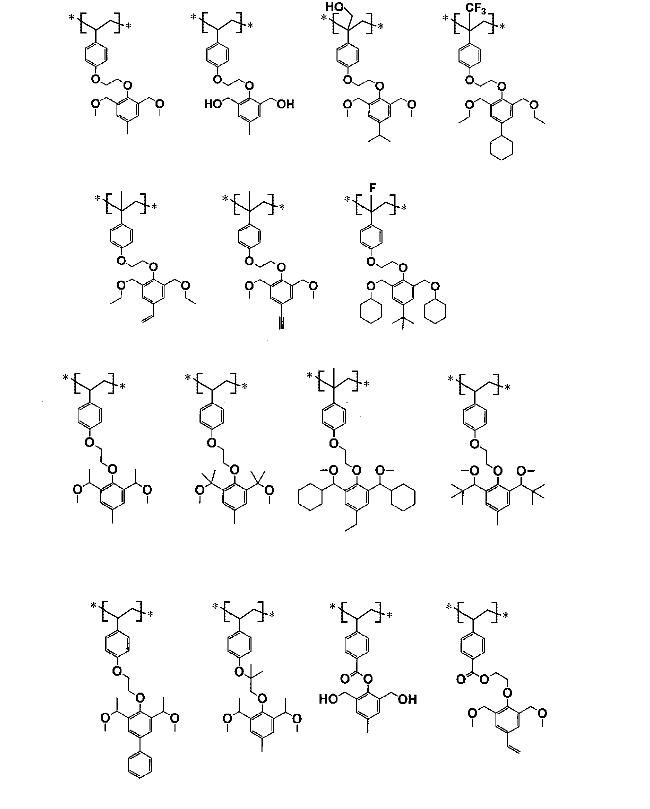
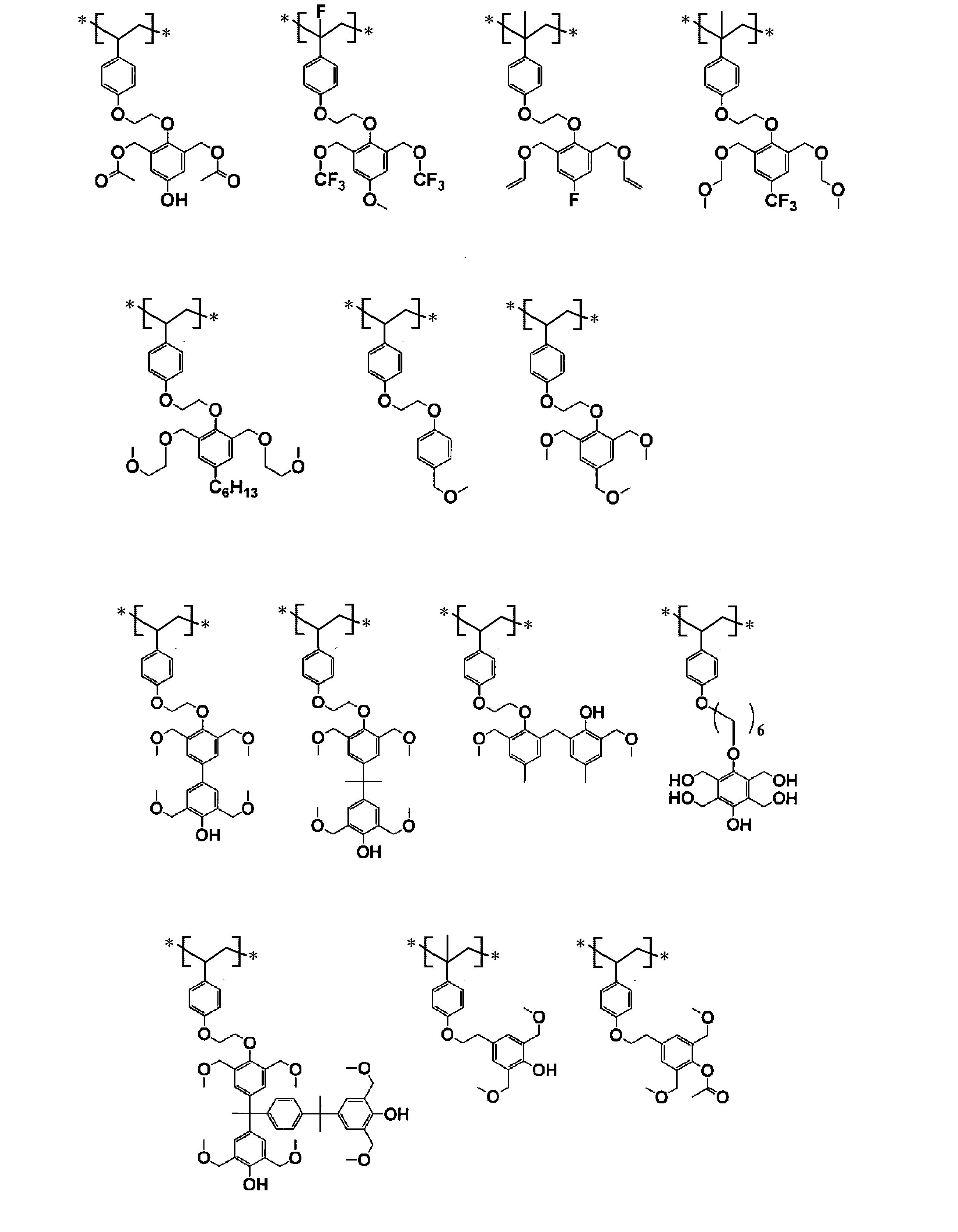
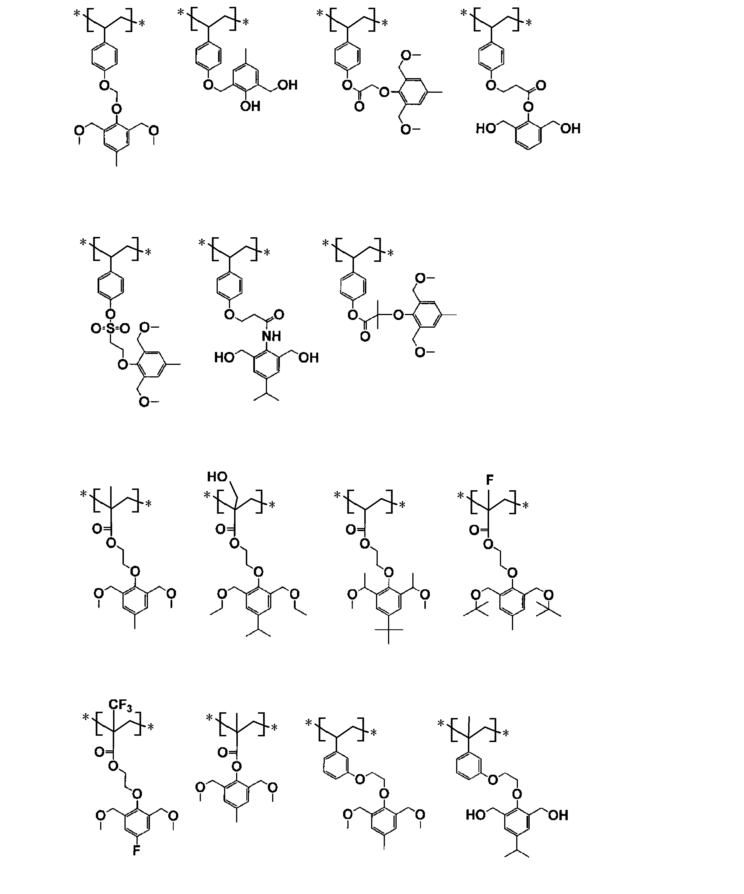


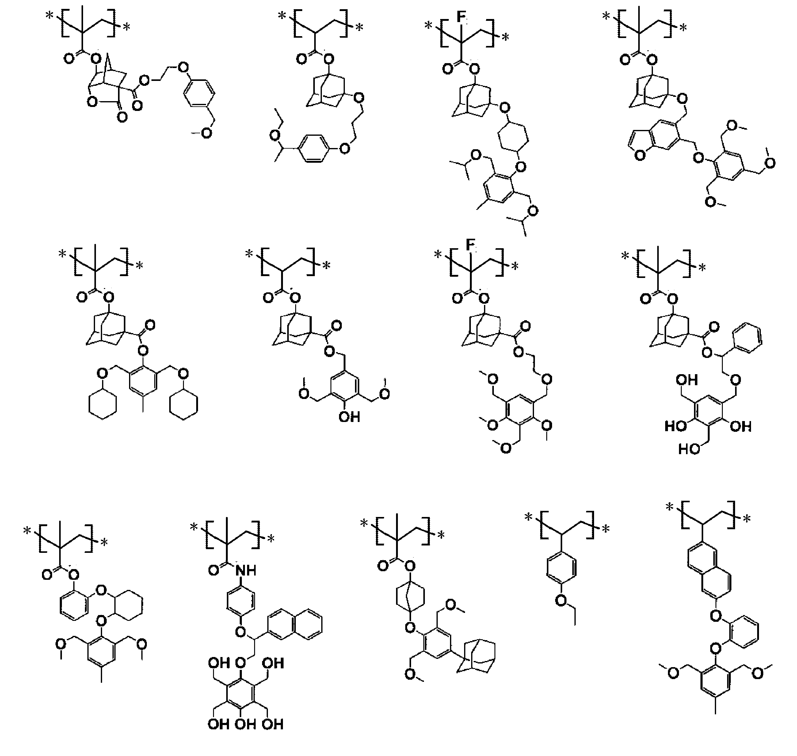


高分子化合物を形成する繰り返し単位(IB)について説明する。
上記一般式(IB)で表される上記繰り返し単位(IB)において、R1bは水素原子、ハロゲン原子又はアルキル基を表す。ハロゲン原子又はアルキル基は、上記R1aのハロゲン原子又はアルキル基と同義であり、好ましいものも同じである。R1bは水素原子が特に好ましい。
L1bは単結合又は連結基を表す。L1bは単結合が好ましい。L1bが連結基である場合、連結基はL1aと同義であるが、好ましくは、カルボニル基、-O-基、-NH-基又はこれらを組み合わせた基(好ましくは総炭素数1~20、より好ましくは総炭素数1~10)であり、さらに好ましくは-CO-O-基、-CO-NH-基である。
Ar1bは、芳香族環を表し、上記L1aの芳香族環と同義であり、好ましいものも同じである。
m1bは、1~5の整数を表し、1~3の整数が好ましく、1が好ましい。


高分子化合物は、繰り返し単位(IA)及び繰り返し単位(IB)以外に、他の繰り返し単位を含んでいてもよい。
他の繰り返し単位は、繰り返し単位(IA)及び繰り返し単位(IB)と共重合可能なものであれば、特に限定されない。例えば、(メタ)アクリル酸エステル、(メタ)アクリル酸、N-置換マレイミド、アクリロニトリル、(メタ)アクリロニトリル、ビニルナフタレン、ビニルアントラセン、インデン等からなる各繰り返し単位が挙げられる。
なお、他の繰り返し単には、上記繰り返し単位(IB)において、Ar1bに結合する水酸基の水素原子が酸により脱離しうる有機基で置換された繰り返し単位は、含まない。酸により脱離しうる有機基としては、酸の作用により脱離して「(Ar1b)-OH」基を生成する有機基等が挙げられる。
高分子化合物が上記他の繰り返し単位を含有する場合、他の繰り返し単位の高分子化合物中の含有率は、高分子化合物を構成する全繰り返し単位に対して、1~20モル%が好ましく、2~10モル%がより好ましい。
高分子化合物は、ラジカル重合法やリビングラジカル重合法、リビングアニオン重合法で合成したポリマーに、架橋性基Xを含む基、例えば、-L2a-(X)m2a基を、高分子反応で修飾して、合成することが好ましい。
特に、架橋性基Xとして、オキシラン、オキセタンを有する場合は、ラジカル重合法やリビングラジカル重合法、リビングアニオン重合法で合成したポリマーに、アルケンを含む多環構造を有する基を高分子反応で修飾した後、酸化剤(例えば、過酸化水素水、mCPBA等)による酸化により、合成することが好ましい。
高分子化合物の分散度(分子量分布)(Mw/Mn)は、好ましくは1.0~3.0であり、より好ましくは1.0~2.0であり、特に好ましくは1.0~1.7である。リビングアニオン重合等のリビング重合によると、高分子化合物の分散度が均一となり、好ましい。高分子化合物の重量平均分子量及び分散度は、GPC測定によるポリスチレン換算値として定義される。


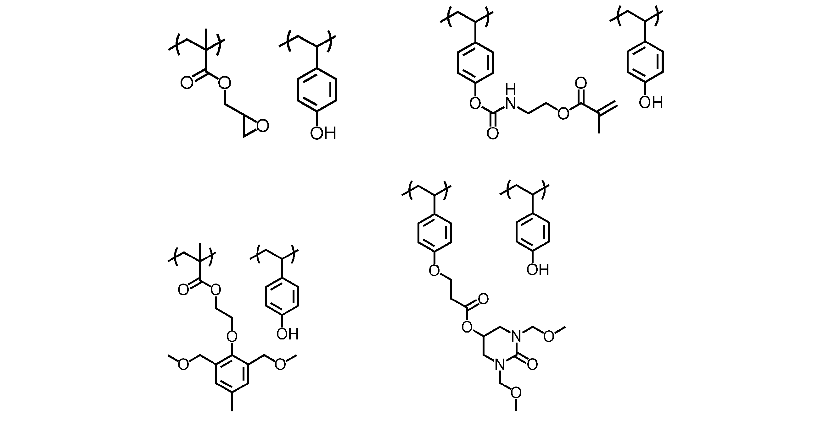

本発明の一つの実施の形態として、高分子化合物は、絶縁層形成用組成物に含有される架橋剤により架橋されてもよい。架橋剤により架橋されているとゲート絶縁層の耐溶媒性や絶縁耐性が向上する。この場合、高分子化合物の架橋物は繰り返し単位(IA)と繰り返し単位(IB)との架橋物でもあり、また繰り返し単位(IB)と架橋剤との架橋物でもある。
架橋剤の官能基数は、特に限定されないが、官能基数が多いほど架橋度が上がるため、好ましくは2~6である。
アルコキシメチル基としては、メトキシメチル基、エトキシメチル基が好ましい。
このようにして合成されたフェノール誘導体のうち、アルコキシメチル基を有するフェノール誘導体が感度、保存安定性の点から特に好ましい。
これら架橋剤の中で特に好ましいものを以下に挙げる。

また、特開2013-214649号公報の[0167]~[0177]に記載の「数平均分子量(Mn)が140~5,000であり、架橋性官能基を有し、フッ素原子を有さない化合物(G)」を用いることも好ましく、これらの内容は好ましくは本願明細書に組み込まれる。
ゲート絶縁層は、上記繰り返し単位(IA)と上記繰り返し単位(IB)とを有する高分子化合物を含有する絶縁層形成用組成物を塗布し、これらの繰り返し単位を架橋反応させて、形成できる。
本発明の絶縁層形成用組成物は、本発明の目的を行わない範囲で、上記繰り返し単位が一部架橋した部分架橋物を含有していてもよい。
本発明の絶縁層形成用組成物において、上記高分子化合物の架橋物の生成を抑えるには、熱又は光を避けるのがよい。
架橋剤を使用する場合、架橋剤の含有率は、高分子化合物に対して、1~40質量%が好ましく、5~20質量%がより好ましい。このようにすることで、未反応の架橋剤によるキャリア移動度の低下をもたらすことなく、架橋密度を高めてゲート絶縁層の耐溶剤性を向上させることができる。
ゲート絶縁層上には、自己組織化単分子膜層を形成することもできる。
自己組織化単分子膜層を形成する化合物としては、自己組織化する化合物であれば特に限定されず、例えば、自己組織化する化合物として、下記式1Sで表される一種類以上の化合物を用いることができる。
式1S:R1S-XS
XSは吸着性又は反応性置換基を表し、具体的には、-SiX4X5X6基(X4は、ハライド基又はアルコキシ基を表し、X5、X6はそれぞれ独立にハライド基、アルコキシ基、アルキル基、アリール基を表す。X4、X5、X6はそれぞれ同じであることが好ましく、クロロ基、メトキシ基、エトキシ基であることがより好ましい)、ホスホン酸基(-PO3H2)、ホスフィン酸基(-PRO2H、Rはアルキル基)、リン酸基、亜リン酸基、アミノ基、ハライド基、カルボキシ基、スルホン酸基、ホウ酸基(-B(OH)2)、ヒドロキシ基、チオール基、エチニル基、ビニル基、ニトロ基又はシアノ基のいずれかを表す。
例えば、より緻密な自己組織化単分子膜層を得る好ましい方法として、Langmuir 19, 1159 (2003)及びJ. Phys. Chem. B 110, 21101 (2006)等に記載の方法が挙げられる。
脱水溶媒としては、特に限定されないが、例えば、クロロホルム、トリクロロエチレン、アニソール、ジエチルエーテル、ヘキサン、トルエン等を単独又は混合して用いることかできる。
さらに、乾燥雰囲気中又は乾燥気体の噴きつけによって、膜を乾燥させることが好ましい。乾燥気体には窒素等の不活性気体を用いるのが好ましい。このような自己組織化単分子膜層の製造方法を用いることにより、緻密で凝集や欠損のない自己組織化単分子膜層が形成されることから、自己組織化単分子膜層の表面粗さを0.3nm以下に抑えることができる。
半導体層は、半導体性を示し、キャリアを蓄積可能な層である。
半導体層は、半導体材料により形成される。有機半導体化合物(単に有機半導体ともいう)で形成される場合、有機半導体層といい、無機半導体化合物(単に無機半導体ともいう)で形成される場合、無機半導体層という。本発明においては、有機半導体層であってもよく、無機半導体層であってもよい。
以下に説明する有機半導体及び無機半導体は、ぞれぞれ、1種を用いても2種以上を併用してもよく、また、有機半導体と無機半導体を併用してもよい。
有機半導体層は、有機半導体を含有する層であればよい。
有機半導体としては、特に限定されず、有機ポリマー及びその誘導体、低分子化合物等が挙げられる。
本発明において、低分子化合物は、有機ポリマー及びその誘導体以外の化合物を意味する。すなわち、繰り返し単位を有さない化合物をいう。低分子化合物は、このような化合物である限り、分子量は特に限定されるものではない。低分子化合物の分子量は、好ましくは300~2000であり、さらに好ましくは400~1000である。

ZA1及びZA2は、S、O、Se又はTeを表す。
nA1及びnA2は0~3の整数を表す。ただし、nA1及びnA2が同時に0になることはない。
これらの置換基は、さらに置換基を複数有していてもよい。複数有していてもよい置換基としては、上記、RA1~RA6で表される置換基が挙げられる。
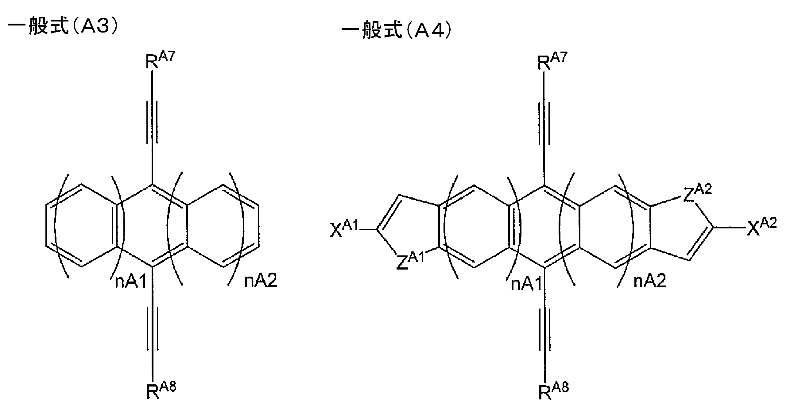
ZA1及びZA2は、S、O、Se又はTeを表す。
nA1及びnA2は0~3の整数を表す。ただし、nA1とnA2が同時に0になることはない。


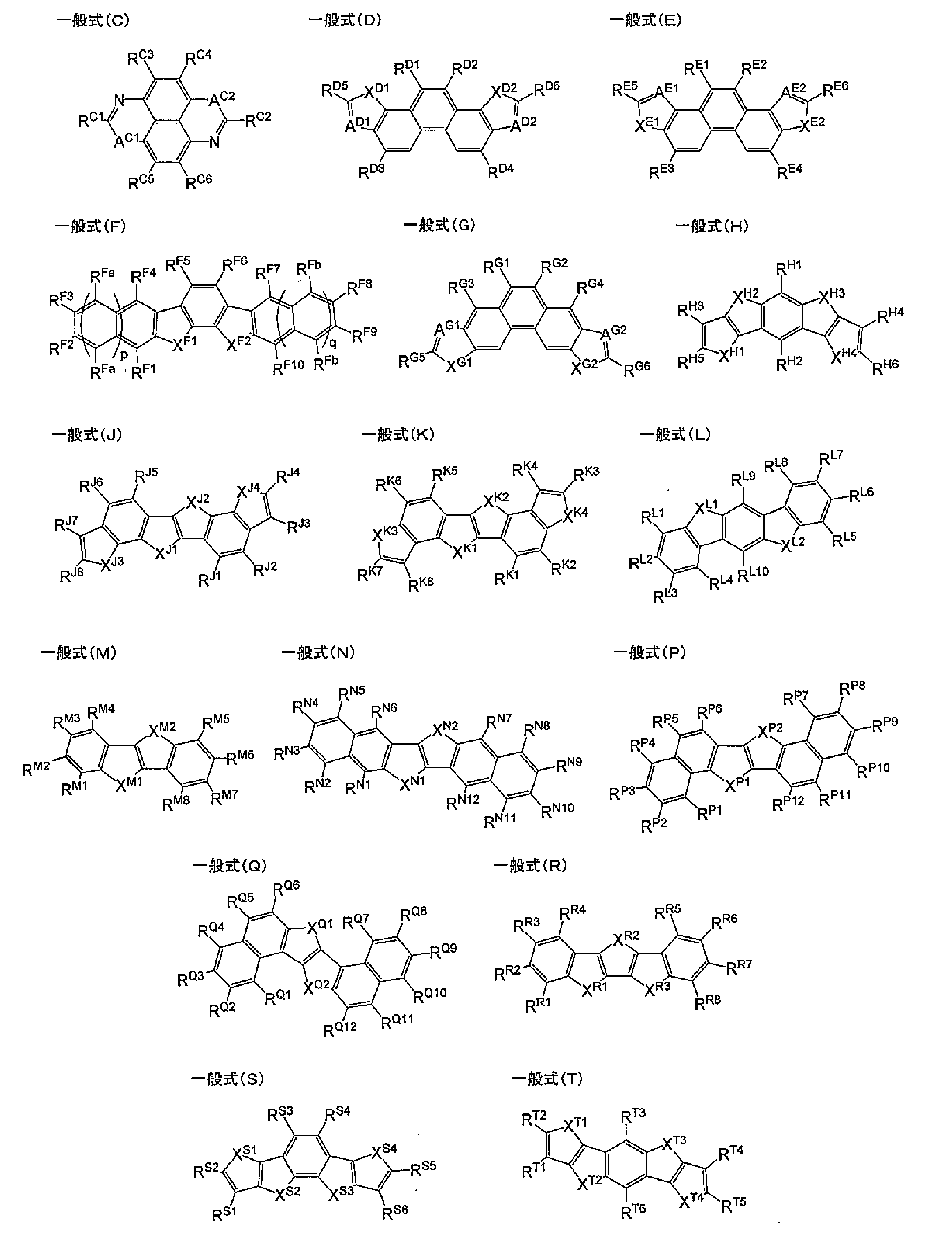
一般式(D)中、XD1及びXD2はNRD9、酸素原子又は硫黄原子を表す。AD1はCRD7又はN原子を表し、AD2はCRD8又はN原子を表し、RD9は水素原子、アルキル基、アルケニル基、アルキニル基又はアシル基を表す。RD1~RD8は水素原子又は置換基を表し、RD1~RD8のうち少なくとも1つが下記一般式(W)で表される置換基である。
一般式(E)中、XE1及びXE2は酸素原子、硫黄原子又はNRE7を表す。AE1及びAE2はCRE8又は窒素原子を表す。RE1~RE8は水素原子又は置換基を表す。RE1~RE8のうち少なくとも1つが下記一般式(W)で表される置換基である。
一般式(G)中、XG1及びXG2はNRG9、酸素原子又は硫黄原子を表す。AG1はCRG7又はN原子を表す。AG2はCRG8又はN原子を表す。RG9は水素原子、アルキル基、アルケニル基、アルキニル基、アシル基、アリール基又はヘテロアリール基を表す。RG1~RG8は水素原子又は置換基を表す。RG1~RG8のうち少なくとも1つが下記一般式(W)で表される置換基である。
一般式(K)中、XK1及びXK2は酸素原子、硫黄原子、セレン原子又はNRK9を表す。XK3及びXK4は酸素原子、硫黄原子又はセレン原子を表す。XK1、XK2、XK3及びXK4は好ましくは硫黄原子を表す。RK1~RK9は水素原子又は置換基を表す。RK1~RK9のうち少なくとも1つが下記一般式(W)で表される置換基である。
一般式(L)中、XL1及びXL2は酸素原子、硫黄原子又はNRL11を表す。XL1及びXL2は好ましくは酸素原子又は硫黄原子を表す。RL1~RL11は水素原子又は置換基を表し、RL1~RL11のうち少なくとも1つが下記一般式(W)で表される置換基である。
一般式(N)中、XN1及びXN2は酸素原子、硫黄原子、セレン原子又はNRN13を表す。XN1及びXN2は好ましくは硫黄原子を表す。RN1~RN13は水素原子又は置換基を表す。RN1~RN13のうち少なくとも1つは下記一般式(W)で表される置換基である。
一般式(P)中、XP1及びXP2は酸素原子、硫黄原子、セレン原子又はNRP13を表す。XP1及びXP2は好ましくは硫黄原子を表す。RP1~RP13は水素原子又は置換基を表す。RP1~RP13のうち少なくとも1つは下記一般式(W)で表される置換基である。
一般式(R)中、XR1、XR2及びXR3は酸素原子、硫黄原子、セレン原子又はNRR9を表す。XR1、XR2及びXR3は好ましくは硫黄原子を表す。RR1~RR9は水素原子又は置換基を表す。RR1~RR9のうち少なくとも1つは下記一般式(W)で表される置換基である。
一般式(T)中、XT1、XT2、XT3、及びXT4は酸素原子、硫黄原子、セレン原子又はNRT7を表す。XT1、XT2、XT3及びXT4は好ましくは硫黄原子を表す。RT1~RT7は水素原子又は置換基を表す。RT1~RT7のうち少なくとも1つは下記一般式(W)で表される置換基である。
また、ヘテロアリール基は、RA1~RA6の置換基で説明したヘテロアリール基と同義である。
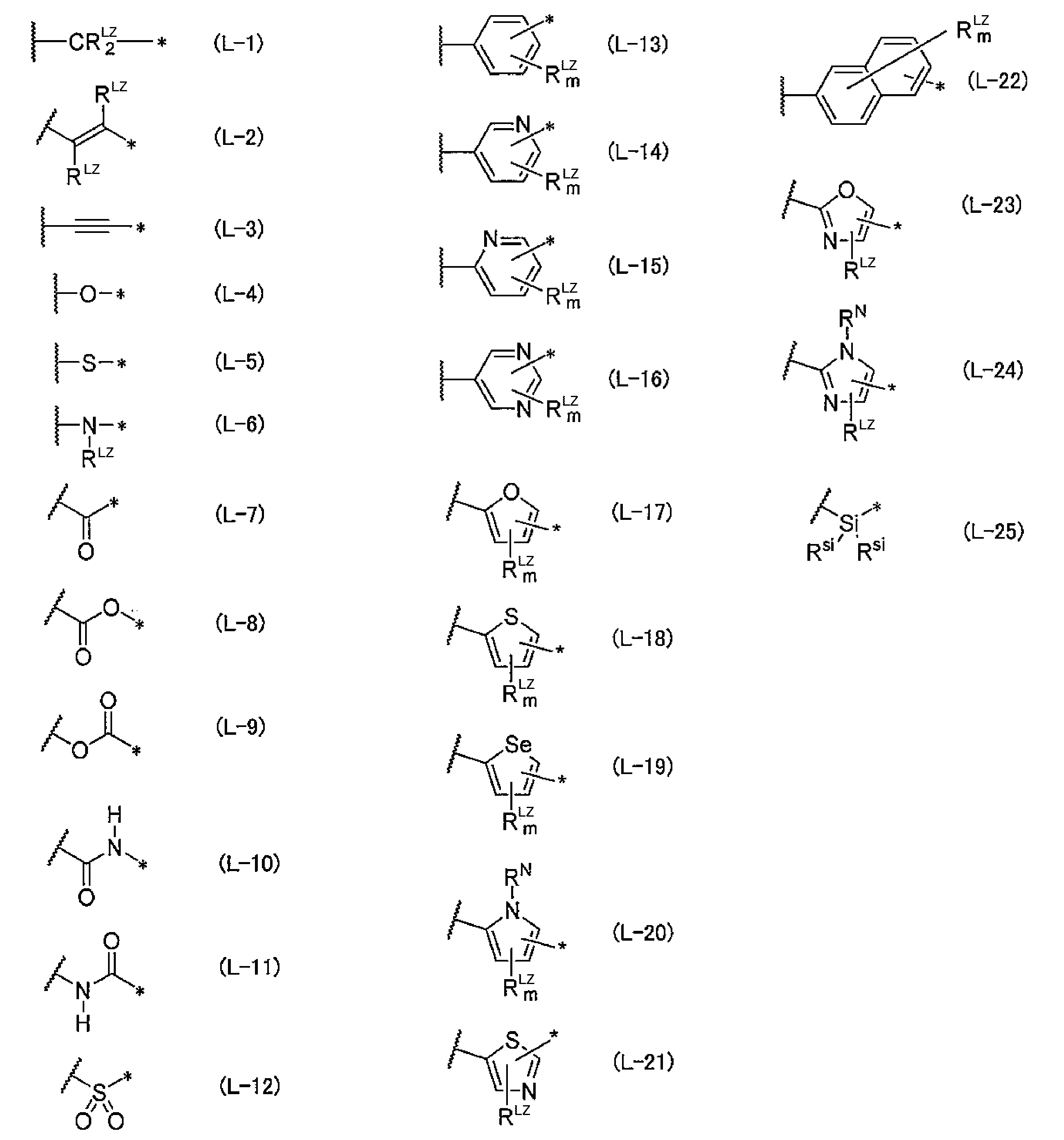
*はRwとの結合位置又は一般式(L-1)~(L-25)の波線部分との結合位置を表す。
一般式(L-13)におけるmは4を表し、一般式(L-14)及び(L-15)におけるmは3を表し、一般式(L-16)~(L-20)におけるmは2を表し、(L-22)におけるmは6を表す。
一般式(L-1)、(L-2)、(L-6)及び(L-13)~(L-24)におけるRLZはそれぞれ独立に水素原子又は置換基を表し、一般式(L-1)及び(L-2)中のRLZはそれぞれLに隣接するRWと結合して縮合環を形成してもよい。
RNは水素原子又は置換基を表し、Rsiはそれぞれ独立に水素原子、アルキル基、アルケニル基又はアルキニル基を表す。

本発明では、主鎖が炭素数N個の置換又は無置換のアルキル基が置換基の末端に存在する場合は、置換基の末端から可能な限りの連結基を含めた上で一般式(W)における-L-RWと解釈することとし、一般式(W)における-RW単独とは解釈しない。具体的には「一般式(W)におけるLに相当する(L-1)1個」と「一般式(W)におけるRWに相当する主鎖が炭素数N-1個の置換又は無置換のアルキル基」とが結合した置換基として解釈する。例えば、炭素数8のアルキル基であるn-オクチル基が置換基の末端に存在する場合、2個のRLZが水素原子である(L-1)1個と、炭素数7のn-ヘプチル基とが結合した置換基として解釈する。また、一般式(W)で表される置換基が炭素数8のアルコキシ基である場合、-O-である一般式(L-4)で表される連結基1個と、2個のRLZが水素原子である(L-1)で表される連結基1個と、炭素数7のn-ヘプチル基とが結合した置換基として解釈する。
一方、本発明では、オキシエチレン基、オキシエチレン単位の繰り返し数vが2以上のオリゴオキシエチレン基、シロキサン基、ケイ素原子数が2以上のオリゴシロキサン基、あるいは、置換又は無置換のトリアルキルシリル基が置換基の末端に存在する場合は、置換基の末端から可能な限りの連結基を含めた上で、一般式(W)におけるRW単独と解釈する。例えば、-(OCH2CH2)-(OCH2CH2)-(OCH2CH2)-OCH3基が置換基の末端に存在する場合、オキシエチレン単位の繰り返し数vが3のオリゴオキシエチレン基単独の置換基として解釈する。
RNとしては、置換基RC~RTが採りうる置換基として例示したものを挙げることができる。その中でもRNとしては水素原子又はメチル基が好ましい。
Rsiは、アルキル基であることが好ましい。Rsiがとり得るアルキル基としては特に制限はないが、Rsiがとり得るアルキル基の好ましい範囲はRWがシリル基である場合にシリル基がとり得るアルキル基の好ましい範囲と同様である。Rsiがとり得るアルケニル基としては特に制限はないが、置換又は無置換のアルケニル基が好ましく、分枝アルケニル基であることがより好ましく、アルケニル基の炭素数は2~3であることが好ましい。Rsiがとり得るアルキニル基としては特に制限はないが、置換又は無置換のアルキニル基が好ましく、分枝アルキニル基であることがより好ましく、アルキニル基の炭素数は2~3であることが好ましい。
化学的安定性、キャリア輸送性の観点から一般式(L-1)で表される2価の連結基を含む2価の連結基であることが特に好ましく、一般式(L-1)で表される2価の連結基であることがより特に好ましく、Lが一般式(L-18)及び(L-1)で表される2価の連結基であり、(L-1)を介してRWと結合し、RWが置換又は無置換のアルキル基であることがさらにより特に好ましく、Lが一般式(L-18A)及び(L-1)で表される2価の連結基であり、(L-1)を介してRWと結合し、RWが置換又は無置換のアルキル基であることがさらにより特に好ましい。
一般式(W)において、RWに隣接するLが一般式(L-2)及び(L-4)~(L-25)で表される2価の連結基である場合は、RWは置換又は無置換のアルキル基であることがより好ましい。
一般式(W)において、RWに隣接するLが一般式(L-3)で表される2価の連結基である場合は、RWは置換又は無置換のアルキル基、置換又は無置換のシリル基であることが好ましい。
RWがアルキル基を表す場合、直鎖アルキル基でも、分枝アルキル基でも、環状アルキル基でもよいが、直鎖アルキル基であることが、分子の直線性が高まり、キャリア移動度を高めることができる観点から好ましい。
これらの中でも、一般式(W)におけるRWとLの組み合わせとしては、一般式(C)~(T)のLが一般式(L-1)で表される2価の連結基であり、かつ、RWが直鎖の炭素数4~17のアルキル基であるか;あるいは、Lが一般式(L-3)、(L-13)又は(L-18)のいずれか1つで表される2価の連結基と一般式(L-1)で表される2価の連結基が結合した2価の連結基であり、かつ、RWが直鎖のアルキル基であることが、キャリア移動度を高める観点から好ましい。
一方、有機溶媒への溶解度を高める観点からは、RWが分枝アルキル基であることが好ましい。
L及びRWに含まれる炭素数の合計は5~14であることが好ましく、6~14であることがより好ましく、6~12であることが特に好ましく、8~12であることがより特に好ましい。
一般式(C)で表される化合物においては、RC1、RC2、RC3、RC6のいずれかが一般式(W)で表される基であることが好ましく、RC1とRC2との両方又はRC3とRC6の両方が一般式(W)で表される基であることがより好ましい。
一般式(D)で表される化合物においては、RD6が一般式(W)で表される基であることが好ましく、RD5とRD6との両方が一般式(W)で表される基であることがより好ましい。
一般式(E)で表される化合物においては、RE6が一般式(W)で表される基であることが好ましく、RE5とRE6との両方が一般式(W)で表される基であることがより好ましい。また、RE5及びRE6が一般式(W)で表される基以外の置換基である場合、2つのRE7が一般式(W)で表される基であるのも好ましい。
一般式(G)で表される化合物においては、RG5又はRG6が一般式(W)で表される基であることが、キャリア移動度を高め、有機溶媒への溶解性を高める観点から好ましい。
一般式(H)で表される化合物においては、RH4又はRH6が一般式(W)で表される基であるのが好ましく、RH4又はRH6、及び、RH3又はRH5が一般式(W)で表される基であるのがより好ましい。
一般式(K)で表される化合物においては、RK7が一般式(W)で表される基であるのが好ましく、RK7とRK3との両方が一般式(W)で表される基であるのがより好ましい。
一般式(L)で表される化合物においては、RL2、RL3、RL6及びRL7のうち少なくとも一つが一般式(W)で表される基であるのがより好ましい。
一般式(N)で表される化合物においては、RN3が一般式(W)で表される基であるのが好ましく、RN3とRN9との両方が一般式(W)で表される基であるのがより好ましい。
一般式(P)で表される化合物においては、RP2又はRP3が一般式(W)で表される基であるのが好ましく、RP2とRP8との両方又はRP3とRP9との両方が一般式(W)で表される基であるのがより好ましい。
一般式(R)で表される化合物においては、RR2が一般式(W)で表される基であるのが好ましく、RR2とRR7との両方が一般式(W)で表される基であるのがより好ましい。
一般式(T)で表される化合物においては、RT2が一般式(W)で表される基であるのが好ましく、RT2とRT5との両方が一般式(W)で表される基であるのがより好ましい。

一方で、薄膜の膜質安定性の観点からは、分子量は300以上であることが好ましく、350以上であることがより好ましく、400以上であることがさらに好ましい。


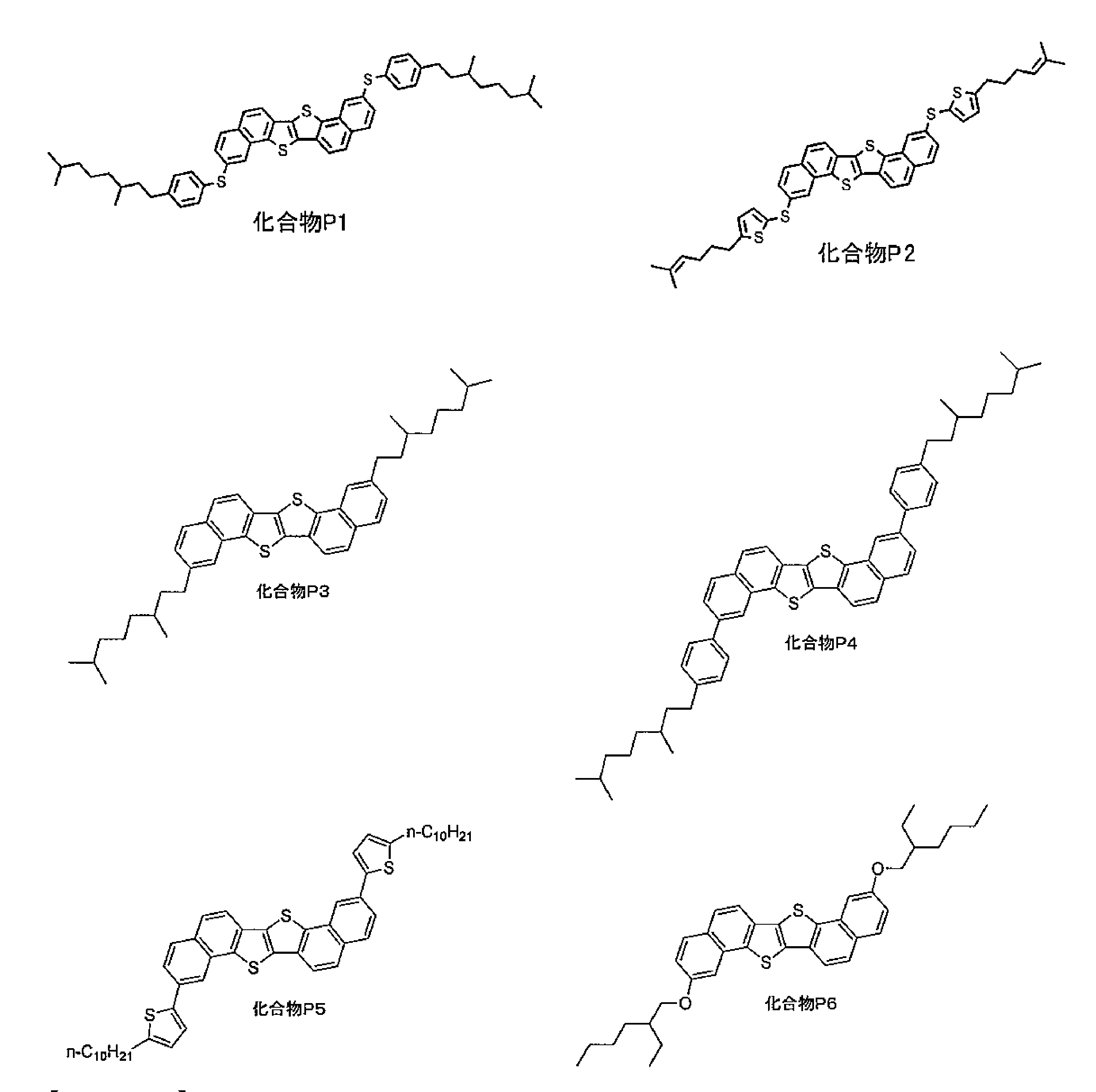
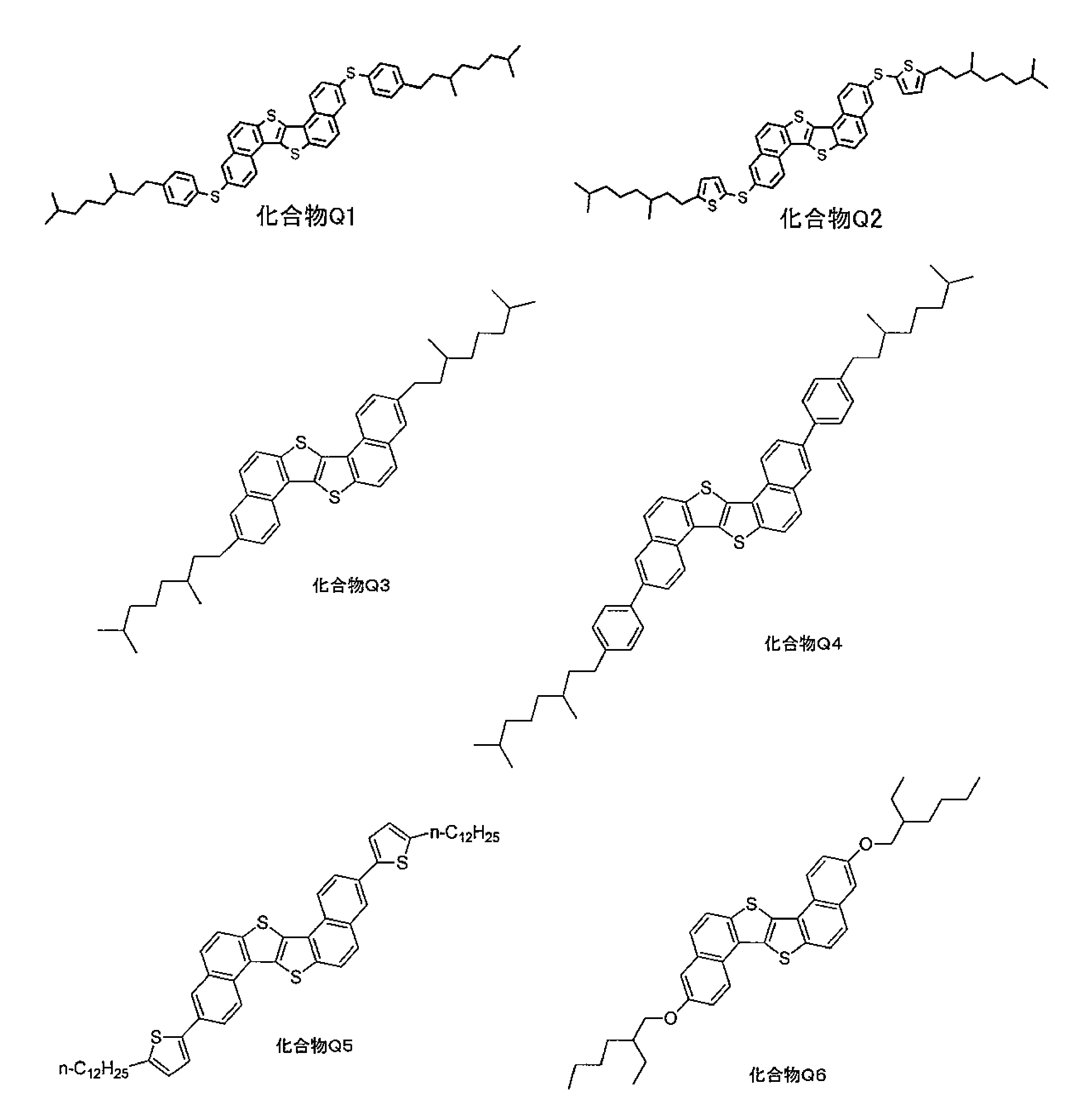


ポリチオフェン及びその誘導体としては、特に限定されないが、例えば、ポリチオフェンにヘキシル基を導入したポリ-3-ヘキシルチオフェン(P3HT)、ポリエチレンジオキシチオフェン、ポリ(3,4-エチレンジオキシチオフェン)/ポリスチレンスルホン酸(PEDOT/PSS)等が挙げられる。
また、これらのポリマーと同じ繰り返し単位を有するオリゴマー(例えば、オリゴチオフェン)を挙げることもできる。
このような高分子化合物としては、一般式(C)~(T)で表される化合物が少なくとも1つ以上のアリーレン基、ヘテロアリーレン基(チオフェン、ビチオフェン等)を介して繰り返し構造を示すπ共役ポリマーや、一般式(C)~(T)で表される化合物が高分子主鎖に側鎖を介して結合したペンダント型ポリマーが挙げられる。高分子主鎖としては、ポリアクリレート、ポリビニル、ポリシロキサン等が好ましく、側鎖としては、アルキレン基、ポリエチレンオキシド基等が好ましい。ペンダント型ポリマーの場合、高分子主鎖は置換基RC~RTの少なくとも1つが重合性基由来の基を有し、これが重合してなるものであってもよい。
湿式法としては、特に限定されないが、例えば、スピンコート法、インクジェット法、ノズルプリント、スタンプ印刷、スクリーン印刷、グラビア印刷、エレクトロスプレイデポジション法等により半導体材料を塗布した後、乾燥させることにより形成することができる。
結晶化処理の方法としては、特に限定されないが、ホットプレート、オーブン等による加熱又はレーザー照射等が挙げられる。加熱温度については、結晶化が進行しやすい点では高温が好ましく、また、一方で、基板等に熱の影響を与え難い点では低温が好ましい。具体的には、50℃以上が好ましく、100℃以上が特に好ましく、また、一方で、300℃以下が好ましく、250℃以下が特に好ましい。
半導体層を形成する無機半導体材料としては、特に限定されないが、塗布型半導体が好ましく、その好ましい例として酸化物半導体が挙げられる。
酸化物半導体としては、金属酸化物からなるものであれば特に限定されない。酸化物半導体からなる半導体層は、酸化物半導体前駆体、すなわち熱酸化等の変換処理によって金属酸化物からなる半導体材料に変換される材料を用いて形成するのが好ましい。
酸化物半導体は特に限定されるものではないが、例えば、酸化インジウムガリウム亜鉛、酸化インジウムガリウム、酸化インジウムスズ亜鉛、酸化ガリウム亜鉛、酸化インジウムスズ、酸化インジウム亜鉛、酸化スズ亜鉛、酸化亜鉛、酸化スズ、例えば、InGaZnOx、InGaOx、InSnZnOx、GaZnOx、InSnOx、InZnOx、SnZnOx(いずれもx>0)、ZnO、SnO2が挙げられる。
酸化物半導体前駆体の具体例としては、例えば、硝酸インジウム、硝酸亜鉛、硝酸ガリウム、硝酸スズ、硝酸アルミニウム、塩化インジウム、塩化亜鉛、塩化スズ(2価)、塩化スズ(4価)、塩化ガリウム、塩化アルミニウム、トリ-i-プロポキシインジウム、ジエトキシ亜鉛、ビス(ジピバロイルメタナト)亜鉛、テトラエトキシスズ、テトラ-i-プロポキシスズ、トリ-i-プロポキシガリウム、トリ-i-プロポキシアルミニウムが挙げられる。
本発明のTFTにおいて、ソース電極は、配線を通じて外部から電流が流入する電極である。また、ドレイン電極は、配線を通じて外部に電流を送り出す電極であり、通常、上記半導体層に接して設けられる。
ソース電極及びドレイン電極の材料としては、従来の有機薄膜トランジスタに用いられている導電性材料を用いることができ、例えば、上記ゲート電極で説明した導電性材料等が挙げられる。
特に、ゲート絶縁層がエッチング液や剥離液に対する耐性に優れていることから、ソース電極及びドレイン電極はエッチング法でも好適に形成することができる。エッチング法は、導電性材料を成膜した後に不要部分をエッチングにより除去する方法である。エッチング法によりパターニングすると、レジスト除去時に下地に残った導電性材料の剥がれ、レジスト残渣や除去された導電性材料の下地への再付着を防止でき、電極エッジ部の形状に優れる。この点で、リフトオフ法よりも好ましい。
ソース電極とドレイン電極との間の間隔(チャネル長)は、任意であるが、100μm以下が好ましく、50μm以下が特に好ましい。また、チャネル幅は、5000μm以下が好ましく、1000μm以下が特に好ましい。
本発明のTFTは、オーバーコート層を有していてもよい。オーバーコート層は、通常、TFTの表面に保護層として形成される層である。単層構造でも多層構造でもよい。
オーバーコート層は、有機系のオーバーコート層でも無機系のオーバーコート層でもよい。
有機系のオーバーコート層を形成する材料としては、特に限定されないが、例えば、ポリスチレン、アクリル樹脂、ポリビニルアルコール、ポリオレフィン、ポリイミド、ポリウレタン、ポリアセナチレン、エポキシ樹脂等の有機ポリマー、及び、これらの有機ポリマーに架橋性基や撥水基等を導入した誘導体等が挙げられる。これらの有機ポリマーやその誘導体は、架橋成分、フッ素化合物、シリコン化合物等と併用することもできる。
無機系のオーバーコート層を形成する材料としては、特に限定されないが、酸化ケイ素、酸化アルミニウム等の金属酸化物、窒化ケイ素等の金属窒化物等が挙げられる。
これらの材料は、1種を用いても、2種以上を任意の組み合わせ及び比率で併用してもよい。
例えば、有機系のオーバーコート層は、例えば、その下地となる層に、オーバーコート層となる材料を含む溶液を塗布後に乾燥させる、オーバーコート層となる材料を含む溶液を塗布、乾燥後に露光、現像してパターニングする等の方法により形成することができる。なお、オーバーコート層のパターニングは、印刷法やインクジェット法等により直接形成することもできる。また、オーバーコート層のパターニング後に、露光や加熱することにより、オーバーコート層を架橋させてもよい。
一方、無機系のオーバーコート層は、スパッタリング法、蒸着法等の乾式法やゾルゲル法のような湿式法により形成することができる。
本発明のTFTは、上記以外の層や部材を設けてもよい。
その他の層又は部材としては、例えば、バンク等が挙げられる。バンクは、インクジェット法等により半導体層やオーバーコート層等を形成するときに、吐出液を所定の位置に塞き止める目的等で用いられる。このため、バンクには、通常、撥液性がある。バンクの形成方法としては、フォトリソグラフィー法等によりパターニングした後にフッ素プラズマ法等の撥液処理を施す方法、フッ素化合物等の撥液成分を含む感光性組成物等を硬化させる方法等が挙げられる。
本発明の有機薄膜トランジスタの場合、ゲート絶縁層が有機層であることから、後者の撥液成分を含む感光性組成物を硬化させる方法が、ゲート絶縁層が撥液処理の影響を受ける可能性がなく、好ましい。なお、バンクを用いずに下地に撥液性のコントラストを持たせてバンクと同じ役割を持たせる技術を用いてもよい。
本発明のTFTは、ゲート電極、ゲート絶縁層、半導体層、ソース電極及びドレイン電極等を、上記した方法により、基板上に成膜又は設けて、製造できる。
特に、ゲート絶縁層や半導体層を形成する材料として有機材料を用いると、溶液塗布法の利点を生かしつつ、上記の優れた特性を発揮するTFTを製造することができる。
本発明の有機薄膜トランジスタの用途の一例として表示パネルが挙げられる。表示パネルとしては、例えば、液晶パネル、有機ELパネル、電子ペーパーパネル等が挙げられる。
各高分子化合物について、ゲル浸透クロマトグラフィー(GPC、東ソー社製;HLC-8120;Tskgel Multipore HXL-M)を用い、溶媒としてTHFを使用して、重量平均分子量(Mw、標準ポリスチレン換算)を測定した。
また、NMR測定装置(ブルカー・バイオスピン社製;AVANCEIII400型)を用い、1H-NMR又は13C-NMRにより、各高分子化合物の組成比(モル比)を算出した。なお、組成比の記載は化学式で示した繰り返し単位の記載に対応する。
得られた結果を以下に示す。


化合物C16は、一般式(C)で表される化合物あり、下記化合物C1の下記合成方法に準じて、合成した。

1,5-ジアミノナフタレン(10g)のピリジン溶液(125mL)に、p-トルエンスルホニルクロリド(34g)をゆっくりと添加し、室温で2時間撹拌した。反応液を氷水に注ぎ、析出物を減圧ろ過した。得られた粗結晶をメタノールで洗浄し、化合物C1a(29g)を得た。
化合物C1a(10g)の氷酢酸溶液を95℃で加熱撹拌し、そこに氷酢酸10mLで希釈した臭素(2mL)をゆっくりと滴下した。10分間反応させ、放冷後にろ過することで粗結晶を灰色固体として得た。粗結晶をニトロベンゼン中で再結晶することで化合物C1b(6.8g)を得た。
化合物C1b(5g)の濃硫酸溶液を室温で24時間撹拌した。反応液を氷水に注ぎ、析出している固体をろ過して回収した。その固体を氷水中に再度分散し、アンモニア水で中和し、化合物C1c(0.5g)を得た。
室温下、化合物C1c(2g)のピリジン溶液にペンタノイルクロリド(バレリン酸クロリド)(2.6mL)を滴下して2時間撹拌した。氷水に反応液を注ぎ、固体を減圧ろ過した。メタノール中に分散し1時間撹拌した後、固体をろ過することで化合物C1d(1.39g)を得た。
THF(360mL)及びトルエン(72mL)の混合溶液中に化合物C1d(1.2g)とローソン試薬(1.48g)を添加した後、加熱還流しながら3時間撹拌した。エバポレーションでTHFのみ除去してトルエン溶液とした後、60℃で1時間撹拌した。その後、不溶物をろ過することで化合物C1e(0.5g)を得た。
化合物C1e(0.4g)と炭酸セシウム(1.33g)をジメチルアセトアミド中、120℃で2時間反応させた。反応液を水に注ぎ析出物をろ過した。ろ過した固体をTHF中で再結晶を繰り返し、目的化合物C1(0.12g)を合成した。得られた化合物C1の同定は、1H-NMR及びMassスペクトルにより行った。
[ボトムゲート形態のOTFTの製造]
図1(B)に示すボトムゲート-トップコンタクト形態のOTFTを製造した。
厚さ0.7mmのガラス基板上に膜厚100nmの酸化インジウムスズ(ITO)膜を形成したITO電極付きガラス基板をアセトン、イソプロピルアルコールで洗浄し、乾燥させた。これを基板6として、用いた。
ゲート絶縁層2の形成に際して絶縁層形成用組成物を調製した。すなわち、下記表1に示す高分子化合物5gと下記表1に示す含有量の架橋剤CA1とをそれぞれ1-ブタノール/エタノール=1/1(体積比)の混合溶媒に溶解させた。この溶解液をφ0.2μmのポリテトラフルオロエチレン(PTFE)メンブランフィルタでろ過して、絶縁層形成用組成物を調製した。
上記ガラス基板6のITO電極(ゲート電極5)上に絶縁層形成用組成物をスピンコート法で塗布し、送風乾燥機により180℃で30分加熱して、層厚300nmのゲート絶縁層2を設けた。
このようにして、図1(B)に示されるOTFT(試料No.1-1~1-16及び比較のためのc1-1~c1-4)を、それぞれ、製造した。
上記試料それぞれと同じ方法により形成したゲート絶縁層又は下記方法により形成した絶縁層について、その特性を評価した。その結果を表1に示す。
上記試料それぞれと同じ方法により形成した各ゲート絶縁層上に厚さ100nmの金電極を真空蒸着により形成した。これをサンプルとして、誘電体測定システム126096W型(ソーラトロン社製)を用いて、比誘電率を測定した。
上記試料それぞれと同じ方法により形成した各ゲート絶縁層上に厚さ100nmの金電極を真空蒸着により形成した。これをサンプルとして、6517B型エレクトロメータ/絶縁抵抗計(Keithley社製)を用いて、体積抵抗率(Ω・cm)を測定した。
上記試料それぞれに用いた絶縁層形成用組成物をシリコンウェハ上にスピンコートした後、ホットプレートを用いて90℃で2分間プリベークして、厚さ300nmの膜を形成した。次いで、空気中において130℃で1時間加熱することにより、絶縁層が形成されたシリコンウェハからなるサンプルを得た。
得られたサンプルの絶縁層の表面を原子間力顕微鏡(AMF)にて観察し、表面粗さ(算術平均粗さRa)を測定した。測定されたRaを下記評価基準により評価した。上記サンプルの評価結果をOTFTのゲート絶縁層の評価とした。本試験において、評価がA又はBであることが求められ、Aであることが好ましい。
A:0.5nm以下
B:0.5nmを超え、1.0nm以下
C:1.0nmを超え、1.5nm以下
D:1.5nmを超える
上記試料それぞれと同じ方法により、各ゲート絶縁層を形成したガラス基板を、トルエン中に12時間浸漬させ、ゲート絶縁層の浸漬前後の層厚を測定した。浸漬前後の層厚変化率を下記式から算出し、下記評価基準により評価した。本試験において、評価がA、A-、又はBであることが求められ、A、またはA-であることが好ましく、Aであることがより好ましい。
浸漬前後の膜厚変化率(%)=浸漬後の膜厚(μm)/浸漬前の膜厚(μm)×100
A :95%以上100%以下
A-:90を超え、95%以下
B :80を超え、90%以下
C :60を超え、80%以下
D :60%以下
製造した各OTFTの特性について、下記評価をした。その結果を表1に示す。
各OTFTのソース電極3及びドレイン電極4間に-40Vの電圧を印加し、ゲート電圧Vgを40V~-40Vの範囲で変化させ、ドレイン電流Idを表す下記式を用いてキャリア移動度μ(cm2/Vs)を算出し、下記評価基準により、評価した。本試験において、評価がA、A-、又はBであることが求められ、A、またはA-であることが好ましく、Aであることがより好ましい。
式中、Lはゲート長、wはゲート幅、Ciはゲート絶縁層2の単位面積当たりの容量、Vgはゲート電圧、Vthは閾値電圧を、それぞれ、表す。
A :0.7cm2/Vsを超え、0.8cm2/Vs以下
A-:0.5cm2/Vsを超え、0.7cm2/Vs以下
B :0.3cm2/Vsを超え、0.5cm2/Vs以下
B-:0.1cm2/Vsを超え、0.3cm2/Vs以下
C :0.05cm2/Vsを超え、0.10cm2/Vs以下
D :0.01cm2/Vs以上、0.05cm2/Vs以下
各OTFTのソース電極3及びドレイン電極4間にかかる電圧を-40Vに固定し、ゲート電圧Vgを40V~-40Vまで変化させた時の(|Id|の最大値)/(|Id|の最小値)をon/off比とした。本試験において、評価がA、A-、又はBであることが求められ、A、またはA-であることが好ましく、Aであることがより好ましい。
A :1×10⁷以上
A-:5×10⁶以上1×10⁷未満
B :1×10⁶以上5×10⁶未満
B-:5×10⁵以上1×10⁶未満
C :1×10⁵以上5×10⁵未満
D :1×10⁵未満

このように本発明の絶縁層形成用組成物で形成したゲート絶縁層2は、上記高分子化合物の硬化物を含有し、高い表面平滑性及び絶縁性を両立していた。したがって、このゲート絶縁層2を半導体層に隣接して設けた本発明のOTFTは、いずれも、一般式(IA)及び一般式(IB)で表される繰り返し構造を有しない高分子化合物の硬化物で形成されたゲート絶縁層を備えた比較のためのOTFTに比べて、キャリア移動度μ及びon/off比が高く、優れた性能を有していた。
また、本発明によるOTFTの上記性能向上効果は、高分子化合物が上記一般式(IA-1)で表される繰り返し単位(IA-1)又は上記一般式(IA-2)で表される繰り返し単位(IA-2)を有していると、さらに増大することが分かった。
[有機半導体を変更したボトムゲート形態のOTFTの製造及び評価]
実施例2では、上記有機半導体以外の有機半導体を用いて、ボトムゲート形態のOTFTを製造し、その特性等を評価した。
すなわち、実施例1において、有機半導体として、上記A26、A27、C1、C4、C7、D1、E2、F2、F5、F10、G12、G14、H10、H11、J2、J3、K2、K3、L2、L5、L6、L8、L9、L15、M3、M8、N4、P3、Q3、R1、S1又はT1を用いたこと以外は実施例1と同様にして、図1(B)に示されるOTFTを、それぞれ、製造した。
製造したOTFTそれぞれについて、実施例1と同様にして、キャリア移動度μ、on/off比及を評価した。その結果、いずれのTFTも、実施例1と同様に優れた特性を有していた。
2 ゲート絶縁層
3 ソース電極
4 ドレイン電極
5 ゲート電極
6 基板
Claims (11)
- 半導体層と該半導体層に隣接する絶縁層とを有する半導体素子であって、
前記絶縁層が、下記一般式(IA)で表される繰り返し単位(IA)と下記一般式(IB)で表される繰り返し単位(IB)とを有する高分子化合物の架橋物で形成されている半導体素子。

一般式(IB)中、R1bは水素原子、ハロゲン原子又はアルキル基を表す。L1bは単結合又は連結基を表し、Ar1bは芳香族環を表す。m1bは1~5の整数を表す。 - 前記L1aが、下記式(1a)で表される請求項1に記載の半導体素子。
式(1a) *-Ar1a-L3a-**
式(1a)中、L3aは単結合又は連結基を表す。Ar1aは芳香族環を表す。*は前記繰り返し単位(IA)の、前記R1aが結合している炭素原子との結合位置を表し、**は前記L2aとの結合位置を表す。 - 前記Ar1aが、ベンゼン環である請求項2に記載の半導体素子。
- 前記繰り返し単位(IA)が、下記一般式(IA-1)で表される繰り返し単位(IA-1)である請求項1~3のいずれか1項に記載の半導体素子。

- 前記繰り返し単位(IA)が、下記一般式(IA-2)で表される繰り返し単位(IA-2)である請求項1~3のいずれか1項に記載の半導体素子。

- 前記架橋基Xが、エポキシ基、オキセタニル基、ヒドロキシメチル基、アルコキシメチル基、(メタ)アクリロイルオキシ基、スチリル基又はビニル基である請求項1~3及び5のいずれか1項に記載の半導体素子。
- 前記架橋基Xが、ヒドロキシメチル基又はアルコキシメチル基である請求項1~3、5及び6のいずれか1項に記載の半導体素子。
- 前記架橋物が、前記繰り返し単位(IA)の前記架橋基Xと繰り返し単位(IB)との架橋反応による架橋物である請求項1~7のいずれか1項に記載の半導体素子。
- 前記架橋物が、ヒドロキシメチル基又はアルコキシメチル基を架橋基として反応形成した架橋部を有する請求項8の半導体素子。
- 前記半導体層が、有機半導体を含有する請求項1~9のいずれか1項に記載の半導体素子。
- 半導体素子の絶縁層を形成するための絶縁層形成用組成物であって、
下記一般式(IA)で表される繰り返し単位(IA)と下記一般式(IB)で表される繰り返し単位(IB)とを有する高分子化合物を含有する絶縁層形成用組成物。

一般式(IB)中、R1bは水素原子、ハロゲン原子又はアルキル基を表す。L1bは単結合又は連結基を表し、Ar1bは芳香族環を表す。m1bは1~5の整数を表す。
Priority Applications (4)
| Application Number | Priority Date | Filing Date | Title |
|---|---|---|---|
| KR1020167029137A KR101879524B1 (ko) | 2014-03-26 | 2015-03-23 | 반도체 소자 및 절연층 형성용 조성물 |
| CN201580016286.5A CN106133886B (zh) | 2014-03-26 | 2015-03-23 | 半导体元件及绝缘层形成用组成物 |
| EP15769500.8A EP3125277B1 (en) | 2014-03-26 | 2015-03-23 | Semiconductor element comprising insulating layer-forming composition |
| US15/259,164 US20170005266A1 (en) | 2014-03-26 | 2016-09-08 | Semiconductor element and insulating layer-forming composition |
Applications Claiming Priority (2)
| Application Number | Priority Date | Filing Date | Title |
|---|---|---|---|
| JP2014-064561 | 2014-03-26 | ||
| JP2014064561A JP6118287B2 (ja) | 2014-03-26 | 2014-03-26 | 半導体素子及び半導体素子の絶縁層形成用組成物 |
Related Child Applications (1)
| Application Number | Title | Priority Date | Filing Date |
|---|---|---|---|
| US15/259,164 Continuation US20170005266A1 (en) | 2014-03-26 | 2016-09-08 | Semiconductor element and insulating layer-forming composition |
Publications (1)
| Publication Number | Publication Date |
|---|---|
| WO2015146926A1 true WO2015146926A1 (ja) | 2015-10-01 |
Family
ID=54195439
Family Applications (1)
| Application Number | Title | Priority Date | Filing Date |
|---|---|---|---|
| PCT/JP2015/058775 Ceased WO2015146926A1 (ja) | 2014-03-26 | 2015-03-23 | 半導体素子及び絶縁層形成用組成物 |
Country Status (6)
| Country | Link |
|---|---|
| US (1) | US20170005266A1 (ja) |
| EP (1) | EP3125277B1 (ja) |
| JP (1) | JP6118287B2 (ja) |
| KR (1) | KR101879524B1 (ja) |
| CN (1) | CN106133886B (ja) |
| WO (1) | WO2015146926A1 (ja) |
Families Citing this family (4)
| Publication number | Priority date | Publication date | Assignee | Title |
|---|---|---|---|---|
| JP6016821B2 (ja) * | 2014-01-10 | 2016-10-26 | 富士フイルム株式会社 | 有機薄膜トランジスタ、有機半導体薄膜および有機半導体材料 |
| CN107077920B (zh) * | 2014-09-25 | 2019-05-03 | 巴斯夫欧洲公司 | 作为光可交联介电质的醚基聚合物 |
| JP7192577B2 (ja) * | 2019-03-06 | 2022-12-20 | 信越化学工業株式会社 | エポキシ化合物、レジスト組成物及びパターン形成方法 |
| TWI797640B (zh) * | 2020-06-18 | 2023-04-01 | 法商液態空氣喬治斯克勞帝方法研究開發股份有限公司 | 基於矽之自組裝單層組成物及使用該組成物之表面製備 |
Citations (2)
| Publication number | Priority date | Publication date | Assignee | Title |
|---|---|---|---|---|
| JP2014024999A (ja) * | 2012-07-27 | 2014-02-06 | Fujifilm Corp | 樹脂組成物及びそれを用いたパターン形成方法 |
| WO2014030441A1 (ja) * | 2012-08-23 | 2014-02-27 | 富士フイルム株式会社 | ポジ型感光性樹脂組成物、硬化膜の製造方法、硬化膜、有機el表示装置および液晶表示装置 |
Family Cites Families (7)
| Publication number | Priority date | Publication date | Assignee | Title |
|---|---|---|---|---|
| US6686124B1 (en) * | 2000-03-14 | 2004-02-03 | International Business Machines Corporation | Multifunctional polymeric materials and use thereof |
| JP2010163521A (ja) * | 2009-01-14 | 2010-07-29 | Sumitomo Chemical Co Ltd | 絶縁層用樹脂組成物 |
| KR20120021488A (ko) * | 2010-08-03 | 2012-03-09 | 주식회사 동진쎄미켐 | 네가티브 감광성 수지 조성물 |
| DE102010034577B4 (de) * | 2010-08-17 | 2013-01-17 | Fraunhofer-Gesellschaft zur Förderung der angewandten Forschung e.V. | Verfahren zur Herstellung durchschlagfester ultradünner Dielektrika in elektronischen Bauteilen unter Verwendung vernetzbarer polymerer dielektrischer Materialien |
| KR101842735B1 (ko) * | 2010-09-02 | 2018-03-27 | 메르크 파텐트 게엠베하 | 전자 디바이스용 게이트 절연체 층 |
| WO2012161175A1 (ja) | 2011-05-24 | 2012-11-29 | 住友化学株式会社 | 有機薄膜トランジスタ絶縁層材料 |
| JP5514284B2 (ja) * | 2011-12-06 | 2014-06-04 | 富士フイルム株式会社 | マイクロレンズアレイ露光機用組成物を用いた樹脂パターンの製造方法 |
-
2014
- 2014-03-26 JP JP2014064561A patent/JP6118287B2/ja not_active Expired - Fee Related
-
2015
- 2015-03-23 KR KR1020167029137A patent/KR101879524B1/ko not_active Expired - Fee Related
- 2015-03-23 CN CN201580016286.5A patent/CN106133886B/zh not_active Expired - Fee Related
- 2015-03-23 WO PCT/JP2015/058775 patent/WO2015146926A1/ja not_active Ceased
- 2015-03-23 EP EP15769500.8A patent/EP3125277B1/en not_active Not-in-force
-
2016
- 2016-09-08 US US15/259,164 patent/US20170005266A1/en not_active Abandoned
Patent Citations (2)
| Publication number | Priority date | Publication date | Assignee | Title |
|---|---|---|---|---|
| JP2014024999A (ja) * | 2012-07-27 | 2014-02-06 | Fujifilm Corp | 樹脂組成物及びそれを用いたパターン形成方法 |
| WO2014030441A1 (ja) * | 2012-08-23 | 2014-02-27 | 富士フイルム株式会社 | ポジ型感光性樹脂組成物、硬化膜の製造方法、硬化膜、有機el表示装置および液晶表示装置 |
Non-Patent Citations (1)
| Title |
|---|
| See also references of EP3125277A4 * |
Also Published As
| Publication number | Publication date |
|---|---|
| CN106133886B (zh) | 2019-07-30 |
| KR20160134818A (ko) | 2016-11-23 |
| JP6118287B2 (ja) | 2017-04-19 |
| KR101879524B1 (ko) | 2018-07-17 |
| EP3125277B1 (en) | 2020-06-03 |
| JP2015188012A (ja) | 2015-10-29 |
| CN106133886A (zh) | 2016-11-16 |
| EP3125277A4 (en) | 2017-03-29 |
| US20170005266A1 (en) | 2017-01-05 |
| EP3125277A1 (en) | 2017-02-01 |
Similar Documents
| Publication | Publication Date | Title |
|---|---|---|
| JP6140626B2 (ja) | 有機薄膜トランジスタ及びその製造方法 | |
| JP6204580B2 (ja) | 薄膜トランジスタ及び絶縁層形成用組成物 | |
| US10008671B2 (en) | Organic thin-film transistor and method for manufacturing same | |
| JP6255651B2 (ja) | 薄膜トランジスタ | |
| JP6118287B2 (ja) | 半導体素子及び半導体素子の絶縁層形成用組成物 | |
| JP6034326B2 (ja) | 半導体素子及び絶縁層形成用組成物 | |
| JP6110802B2 (ja) | 薄膜トランジスタ | |
| JP6140625B2 (ja) | 有機薄膜トランジスタ | |
| JP6096704B2 (ja) | 熱もしくは光硬化性組成物、並びに、それを用いた絶縁膜及び薄膜トランジスタ |
Legal Events
| Date | Code | Title | Description |
|---|---|---|---|
| 121 | Ep: the epo has been informed by wipo that ep was designated in this application |
Ref document number: 15769500 Country of ref document: EP Kind code of ref document: A1 |
|
| REEP | Request for entry into the european phase |
Ref document number: 2015769500 Country of ref document: EP |
|
| WWE | Wipo information: entry into national phase |
Ref document number: 2015769500 Country of ref document: EP |
|
| NENP | Non-entry into the national phase |
Ref country code: DE |
|
| ENP | Entry into the national phase |
Ref document number: 20167029137 Country of ref document: KR Kind code of ref document: A |