WO2015151512A1 - インターポーザ、半導体装置、インターポーザの製造方法、半導体装置の製造方法 - Google Patents
インターポーザ、半導体装置、インターポーザの製造方法、半導体装置の製造方法 Download PDFInfo
- Publication number
- WO2015151512A1 WO2015151512A1 PCT/JP2015/001854 JP2015001854W WO2015151512A1 WO 2015151512 A1 WO2015151512 A1 WO 2015151512A1 JP 2015001854 W JP2015001854 W JP 2015001854W WO 2015151512 A1 WO2015151512 A1 WO 2015151512A1
- Authority
- WO
- WIPO (PCT)
- Prior art keywords
- hole
- layer
- forming
- insulating resin
- conductive
- Prior art date
- Legal status (The legal status is an assumption and is not a legal conclusion. Google has not performed a legal analysis and makes no representation as to the accuracy of the status listed.)
- Ceased
Links
Images


Classifications
-
- H—ELECTRICITY
- H10—SEMICONDUCTOR DEVICES; ELECTRIC SOLID-STATE DEVICES NOT OTHERWISE PROVIDED FOR
- H10W—GENERIC PACKAGES, INTERCONNECTIONS, CONNECTORS OR OTHER CONSTRUCTIONAL DETAILS OF DEVICES COVERED BY CLASS H10
- H10W70/00—Package substrates; Interposers; Redistribution layers [RDL]
- H10W70/60—Insulating or insulated package substrates; Interposers; Redistribution layers
- H10W70/62—Insulating or insulated package substrates; Interposers; Redistribution layers characterised by their interconnections
- H10W70/63—Vias, e.g. via plugs
- H10W70/635—Through-vias
-
- H—ELECTRICITY
- H10—SEMICONDUCTOR DEVICES; ELECTRIC SOLID-STATE DEVICES NOT OTHERWISE PROVIDED FOR
- H10W—GENERIC PACKAGES, INTERCONNECTIONS, CONNECTORS OR OTHER CONSTRUCTIONAL DETAILS OF DEVICES COVERED BY CLASS H10
- H10W70/00—Package substrates; Interposers; Redistribution layers [RDL]
- H10W70/01—Manufacture or treatment
- H10W70/05—Manufacture or treatment of insulating or insulated package substrates, or of interposers, or of redistribution layers
- H10W70/095—Manufacture or treatment of insulating or insulated package substrates, or of interposers, or of redistribution layers of vias therein
-
- H—ELECTRICITY
- H10—SEMICONDUCTOR DEVICES; ELECTRIC SOLID-STATE DEVICES NOT OTHERWISE PROVIDED FOR
- H10W—GENERIC PACKAGES, INTERCONNECTIONS, CONNECTORS OR OTHER CONSTRUCTIONAL DETAILS OF DEVICES COVERED BY CLASS H10
- H10W70/00—Package substrates; Interposers; Redistribution layers [RDL]
- H10W70/60—Insulating or insulated package substrates; Interposers; Redistribution layers
- H10W70/62—Insulating or insulated package substrates; Interposers; Redistribution layers characterised by their interconnections
- H10W70/65—Shapes or dispositions of interconnections
-
- H—ELECTRICITY
- H10—SEMICONDUCTOR DEVICES; ELECTRIC SOLID-STATE DEVICES NOT OTHERWISE PROVIDED FOR
- H10W—GENERIC PACKAGES, INTERCONNECTIONS, CONNECTORS OR OTHER CONSTRUCTIONAL DETAILS OF DEVICES COVERED BY CLASS H10
- H10W70/00—Package substrates; Interposers; Redistribution layers [RDL]
- H10W70/60—Insulating or insulated package substrates; Interposers; Redistribution layers
- H10W70/62—Insulating or insulated package substrates; Interposers; Redistribution layers characterised by their interconnections
- H10W70/66—Conductive materials thereof
-
- H—ELECTRICITY
- H10—SEMICONDUCTOR DEVICES; ELECTRIC SOLID-STATE DEVICES NOT OTHERWISE PROVIDED FOR
- H10W—GENERIC PACKAGES, INTERCONNECTIONS, CONNECTORS OR OTHER CONSTRUCTIONAL DETAILS OF DEVICES COVERED BY CLASS H10
- H10W70/00—Package substrates; Interposers; Redistribution layers [RDL]
- H10W70/60—Insulating or insulated package substrates; Interposers; Redistribution layers
- H10W70/67—Insulating or insulated package substrates; Interposers; Redistribution layers characterised by their insulating layers or insulating parts
- H10W70/68—Shapes or dispositions thereof
- H10W70/685—Shapes or dispositions thereof comprising multiple insulating layers
-
- H—ELECTRICITY
- H10—SEMICONDUCTOR DEVICES; ELECTRIC SOLID-STATE DEVICES NOT OTHERWISE PROVIDED FOR
- H10W—GENERIC PACKAGES, INTERCONNECTIONS, CONNECTORS OR OTHER CONSTRUCTIONAL DETAILS OF DEVICES COVERED BY CLASS H10
- H10W70/00—Package substrates; Interposers; Redistribution layers [RDL]
- H10W70/60—Insulating or insulated package substrates; Interposers; Redistribution layers
- H10W70/67—Insulating or insulated package substrates; Interposers; Redistribution layers characterised by their insulating layers or insulating parts
- H10W70/69—Insulating materials thereof
-
- H—ELECTRICITY
- H10—SEMICONDUCTOR DEVICES; ELECTRIC SOLID-STATE DEVICES NOT OTHERWISE PROVIDED FOR
- H10W—GENERIC PACKAGES, INTERCONNECTIONS, CONNECTORS OR OTHER CONSTRUCTIONAL DETAILS OF DEVICES COVERED BY CLASS H10
- H10W70/00—Package substrates; Interposers; Redistribution layers [RDL]
- H10W70/60—Insulating or insulated package substrates; Interposers; Redistribution layers
- H10W70/62—Insulating or insulated package substrates; Interposers; Redistribution layers characterised by their interconnections
- H10W70/65—Shapes or dispositions of interconnections
- H10W70/654—Top-view layouts
- H10W70/655—Fan-out layouts
-
- H—ELECTRICITY
- H10—SEMICONDUCTOR DEVICES; ELECTRIC SOLID-STATE DEVICES NOT OTHERWISE PROVIDED FOR
- H10W—GENERIC PACKAGES, INTERCONNECTIONS, CONNECTORS OR OTHER CONSTRUCTIONAL DETAILS OF DEVICES COVERED BY CLASS H10
- H10W74/00—Encapsulations, e.g. protective coatings
- H10W74/10—Encapsulations, e.g. protective coatings characterised by their shape or disposition
- H10W74/15—Encapsulations, e.g. protective coatings characterised by their shape or disposition on active surfaces of flip-chip devices, e.g. underfills
-
- H—ELECTRICITY
- H10—SEMICONDUCTOR DEVICES; ELECTRIC SOLID-STATE DEVICES NOT OTHERWISE PROVIDED FOR
- H10W—GENERIC PACKAGES, INTERCONNECTIONS, CONNECTORS OR OTHER CONSTRUCTIONAL DETAILS OF DEVICES COVERED BY CLASS H10
- H10W90/00—Package configurations
- H10W90/701—Package configurations characterised by the relative positions of pads or connectors relative to package parts
- H10W90/721—Package configurations characterised by the relative positions of pads or connectors relative to package parts of bump connectors
- H10W90/724—Package configurations characterised by the relative positions of pads or connectors relative to package parts of bump connectors between a chip and a stacked insulating package substrate, interposer or RDL
-
- H—ELECTRICITY
- H10—SEMICONDUCTOR DEVICES; ELECTRIC SOLID-STATE DEVICES NOT OTHERWISE PROVIDED FOR
- H10W—GENERIC PACKAGES, INTERCONNECTIONS, CONNECTORS OR OTHER CONSTRUCTIONAL DETAILS OF DEVICES COVERED BY CLASS H10
- H10W90/00—Package configurations
- H10W90/701—Package configurations characterised by the relative positions of pads or connectors relative to package parts
- H10W90/731—Package configurations characterised by the relative positions of pads or connectors relative to package parts of die-attach connectors
- H10W90/734—Package configurations characterised by the relative positions of pads or connectors relative to package parts of die-attach connectors between a chip and a stacked insulating package substrate, interposer or RDL
Definitions
- the present invention relates to an interposer, a semiconductor device, an interposer manufacturing method, and a semiconductor device manufacturing method.
- the interposer is, for example, a component that is disposed and used between a package substrate and an IC chip.
- a technique for interposing an interposer between the package substrate and the IC chip for example, there are those described in Patent Documents 1 to 4.
- JP 2001-102479 A Japanese Patent Laid-Open No. 2002-37362 JP 2002-261204 A JP 2000-332168 A
- interposers especially glass interposers based on glass.
- One of the problems is that the difference in coefficient of thermal expansion between the glass that is the base material and copper or the like used for the conductive layer pattern (for example, the through electrode) is large, and the elastic modulus is large.
- the conductive layer pattern made of copper or the like peels off from the glass surface due to a high temperature process during mounting, a temperature cycle of a reliability test, or the like.
- the present invention is intended to solve such a problem, an interposer, a semiconductor device, which can have sufficient reliability by preventing peeling of a conductive layer pattern due to thermal expansion and thermal contraction, It is an object of the present invention to provide a method for manufacturing an interposer and a method for manufacturing a semiconductor device.
- One embodiment of the present invention is a substrate having a through hole; One or more layers formed on the surface of the base material, and an insulating resin layer having a conductive via; One or more wiring layers disposed on the substrate with the insulating resin layer interposed therebetween; An inorganic adhesion layer formed only on the side surface of the through hole; A through electrode filled in a connection hole formed in the through hole with the inorganic adhesion layer and capable of conducting both sides of the substrate; and The through electrode is electrically connected to the wiring layer through the conductive via,
- the interposer is characterized in that a thermal expansion coefficient of the inorganic adhesion layer is larger than a thermal expansion coefficient of the base material and smaller than a thermal expansion coefficient of the through electrode.
- an interposer that can have sufficient reliability by preventing peeling of a conductive layer pattern (for example, a through electrode) due to thermal expansion and contraction. Become. Further, according to one embodiment of the present invention, a method for manufacturing the interposer, a semiconductor device including the interposer, and a method for manufacturing the semiconductor device can be provided.
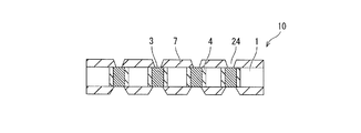
- the interposer 100 includes a base material 1, a through electrode 3, an inorganic adhesion layer 4, a land 6, an insulating resin layer 7, a wiring layer 8, and a conductive via 9. Yes.
- An inorganic adhesion layer 4 may also be provided on the surface of the substrate 1.
- a conductive layer 5 (conductive layer pattern) may be provided on the inorganic adhesion layer 4.
- the base material 1 is a glass substrate (glass base material) mainly composed of SiO 2 and has a through hole 13. Further, the thermal expansion coefficient of the base material 1 is 3 to 4 ppm / ° C.
- the coefficient of thermal expansion was measured by TMA (thermomechanical analysis) according to JIS: R3102 and JIS: K7197.
- a CO 2 laser, a UV laser, a picosecond laser, a femtosecond laser, an excimer laser, electric discharge machining, photosensitive glass, blasting, or the like can be used as a method of forming the through-hole 13 in the base material 1.
- a CO 2 laser, a UV laser, a picosecond laser, a femtosecond laser, an excimer laser, electric discharge machining, photosensitive glass, blasting, or the like can be used. Yes, what is necessary is just to select with the thickness of the base material 1 and the hole diameter of the through-hole 13.
- the through electrode 3 is formed of a conductive material and is disposed in the through hole 13.
- the conductive material forming the through electrode 3 include copper, silver, gold, nickel, platinum, palladium, ruthenium, tin, tin silver, tin silver copper, tin copper, tin bismuth, and tin lead.
- a single metal, or a laminate or compound of any single metal can be used, and a material having high adhesion to the inorganic adhesion layer 4 and high electrical connection stability may be selected.
- a conductive material for forming the through electrode 3 for example, a conductive paste that is a mixture of at least one metal powder and a resin material among the above-described materials can be used.
- the method for forming the through electrode 3 is not particularly defined, but an electroless plating method or an electrolytic plating method can be used.
- the form of the through electrode 3 formed by plating includes a conformal plating form and a filled plating form.
- a through-hole-like hole remains in the center of the through-hole 13, and an insulating resin or a conductive paste may be filled by screen printing.
- an electroless plating layer or an electrolytic plating layer is formed on the surface of the conductive paste as the conductive layer 5, and further, the continuity with the conformal plating film is improved to form the land 6, and the conduction via 9 is ensured. It is also possible.
- an electroless plating layer or an electrolytic plating layer is formed on the surface of the insulating resin to ensure conductivity with the conformal plating film to form the land 6. What is necessary is just to ensure conduction.
- the through electrode 3 for example, after forming the inorganic adhesion layer 4, it is also possible to use a method of filling the conductive paste with a screen printing method to form the through electrode 3.
- the thermal expansion coefficient of copper often used as a conductive material is about 16 ppm / ° C.
- the inorganic adhesion layer 4 is formed on both surfaces of the substrate 1 and in the through holes 13. Further, a portion of the inorganic adhesion layer 4 formed in the through hole 13 is disposed between the through electrode 3 and the inner wall surface (inner diameter surface) of the through hole 13.
- Examples of the material of the inorganic adhesion layer 4 include tin oxide, indium oxide, zinc oxide, which are materials having high adhesion between the base material 1 and the conductive material and having a higher thermal expansion coefficient than the base material 1.
- Nickel thermal expansion coefficient: 15 ppm / ° C
- nickel phosphorus nickel phosphorus
- chromium thermal expansion coefficient: 8 ppm / ° C
- chromium oxide aluminum nitride, aluminum oxide, tantalum
- titanium thermal expansion
- a material such as a rate (9 ppm / ° C.) or copper (thermal expansion coefficient: 16 ppm / ° C.) can be used.
- the inorganic adhesion layer 4 has a higher coefficient of thermal expansion than the base material 1, the stress applied between the layers due to the difference in the linear expansion coefficient between the through electrode 3 and the conductive layer 5 and the base material 1 is reduced. It becomes possible to do.
- the upper limit of the thermal expansion coefficient of the inorganic adhesion layer 4 is desirably lower than the upper limit of the thermal expansion coefficient of the conductive material.
- the inorganic adhesion layer 4 can use the above-mentioned material as a single layer or two or more composite materials such as an ITO film (thermal expansion coefficient: 9 ppm / ° C.) in a single layer. .
- the inorganic adhesion layer 4 can use two or more types of composite materials in a laminated film of two or more layers, such as chromium / copper and titanium / copper.
- the film thickness of the inorganic adhesion layer 4 is not particularly specified, but if it is within the range of 0.1 ⁇ m or more and 1 ⁇ m or less, it is possible to obtain the effect of reducing the difference between the adhesion with the substrate 1 and the thermal expansion coefficient. Is possible.
- the method for forming the inorganic adhesion layer 4 is not particularly defined, a sputtering film forming method, an electroless plating method, or the like can be used.
- the conductive layer 5 is made of a conductive material, and may be disposed on both surfaces of the substrate 1 with the inorganic adhesion layer 4 interposed therebetween.
- Examples of the conductive material for forming the conductive layer 5 include copper, silver, gold, nickel, platinum, palladium, ruthenium, tin, tin silver, tin silver copper, tin copper, tin bismuth, and tin lead.
- a single metal, or a laminate or compound of any single metal can be used, and a material having high adhesion to the inorganic adhesion layer 4 and high electrical connection stability may be selected.
- a conductive material for forming the conductive layer 5 for example, a conductive paste that is a mixture of at least one metal powder and a resin material among the above-described materials can be used.
- the method for forming the conductive layer 5 is not particularly limited, but an electroless plating method or an electrolytic plating method can be used.
- the lands 6 may be formed on the upper and lower ends of the through electrode 3 with the conductive layer 5 interposed therebetween.
- the shape of the land 6 can be, for example, a shape formed at the same height as the surface of the substrate 1 or a shape formed several microns higher than the surface of the substrate 1.
- the method for forming the land 6 is not particularly defined, but after the inside of the through hole 13 is filled with a conductive material or an insulating resin, the conductive layer 5 or the resin filled in the through hole 13 is used as a base material. It is possible to use a method in which the surface 6 is polished and removed to expose the upper and lower ends of the through electrode 3 to form lands 6, or a method in which the conductive layer 5 located at the upper and lower ends of the through electrode 3 is patterned to form lands 6. Is possible.
- the land 6 for example, a method of cutting both ends of the through hole 13 into the shape of the land 6 and filling the conductive material can be used.
- the inorganic adhesion layer 4 other than the portion in contact with the land 6 is removed by polishing or etching processing at the time of patterning.
- the land 6 can be formed by stacking the through electrode 3 as it is.
- the outer diameter of the land 6 is the same as the inner diameter of the through hole 13.
- the outer diameter of the land 6 may be larger than the inner diameter of the through hole 13 in consideration of the processing accuracy of forming the conductive via 9.
- the fluctuation factors of the processing accuracy include expansion / contraction of the base material 1, positional accuracy variation of the processing method of the via hole, and the upper limit of the outer diameter of the land 6 is set to 20 ⁇ m larger than the inner diameter of the through hole 13. In this case, it is possible to obtain good conductivity without the conduction via 9 being dropped from the land 6.
- One or more insulating resin layers 7 are laminated, and the one closest to the base material 1 is formed on the base material 1 or the conductive layer 5.
- the insulating resin layer 7 has a required number of layers stacked. Note that the number of the insulating resin layers 7 may be set by, for example, product design.
- any one of epoxy / phenolic resin, polyimide resin, cycloolefin, and PBO resin, or a composite material in which at least two materials are combined can be used. It is. In this case, for example, when the material of the insulating resin layer 7 is a material having a thermal expansion coefficient of 30 to 100 ppm / ° C. which is higher than that of the conductive material and has a higher elastic modulus, By covering the conductive layer 5, it is possible to reduce the stress applied between the conductive layer 5 and the base material 1 and to impart an effect of suppressing the peeling of the conductive layer 5.
- the wiring layer 8 is formed on the insulating resin layer 7 or sandwiched between adjacent insulating resin layers.
- the wiring layer 8 has a required number of layers stacked. Note that the number of wiring layers 8 may be set by, for example, product design.
- the method for forming the wiring layer 8 is not particularly limited. For example, a method of forming a pattern by a semi-additive method or a subtractive method by electroless plating or thickening by electroplating using a sputtered film as a seed layer. It may be used.
- the conductive via 9 is formed in the insulating resin layer 7 and electrically connects the conductive layer 5 and the wiring layer 8.
- the diameter of the conductive via 9 on the substrate 1 side (the diameter of the bottom) is made smaller than the diameters of the through hole 13 and the through electrode 3.
- the conductive vias 9 can be stacked in a stacked structure, and the number of wirings that can be arranged between the lands 6 can be increased in forming the wiring layer 8 and the land 6 on the insulating resin layer 7. It becomes possible, and it becomes possible to form the hole pitch of the through-hole 13 formed in the base material 1 narrowly.
- the conductive via 9 is formed by performing a process of filling a conductive material such as conformal plating in the via hole formed in the insulating resin layer 7.
- a method of forming a via hole in the insulating resin layer 7 may be selected depending on, for example, the material of the insulating resin layer 7. If the material of the insulating resin layer 7 is a thermosetting resin, for example, a CO 2 laser is used. For example, a desmear process may be performed to remove smear generated by laser processing after the laser processing. Moreover, what is necessary is just to form by the photolithographic method, for example, when the material of the insulating resin layer 7 is a photosensitive resist.
- the interposer 100 of this embodiment is an interposer with a through electrode having a multilayer structure. Further, with the interposer 100 of the present embodiment, high conduction reliability can be realized between the wiring layers 8 formed on both surfaces of the substrate 1. Note that the required number of insulating resin layers 7 and wiring layers 8 shown in FIG. 1 and the shape and height of the metal layer of the conductive pad portion are merely examples, and are not particularly specified.
- the semiconductor device 300 includes an interposer 100 and a semiconductor element 11.
- the interposer 100 is mounted on a printed wiring board (not shown) using solder balls 18.
- the semiconductor element 11 is mounted on one surface (the upper surface in FIG. 2) of the interposer 100 using solder balls (not shown).
- the shape of the semiconductor element 11 shown in FIG. 2 and the connection method between the semiconductor element 11 and the interposer 100 are merely examples, and are not particularly defined.
- by optimizing the material of the conductive pad between the semiconductor element 11 and the interposer 100 to be connected high connection strength can be obtained and heat during mounting can be obtained. By optimizing the deformation, high connection reliability can be realized.
- Example 1-1 Embodiment 1-1 of the present invention will be described below with reference to FIGS. 3 to 8 with reference to FIGS.
- the substrate 1 low expansion glass having a thickness of 0.3 mm, a size of 200 mm ⁇ 200 mm, and a thermal expansion coefficient of 4 ppm / ° C. was used.
- the inorganic adhesion layer 4 was formed by stacking a 0.1 ⁇ m thick Cr film (thermal expansion coefficient: 8 ppm / ° C.) and a 0.2 ⁇ m thick Cu film by sputtering.
- the electrolytic copper plating layer 2 (thermal expansion coefficient: 16 ppm / ° C.) was formed using a conductive material.
- the through electrode 3 was formed with a filled copper plating configuration.
- the material for the insulating resin layer 7 ABF made of epoxy resin was used.
- electroless copper plating was used for the seed layer, the thickness of the electrolytic copper plating was 8 ⁇ m, the LS value of the wiring layer 8 was 10 ⁇ m, and the wiring layer 8 was formed by a semi-additive method.
- the conductive via 9 was formed by conformal plating.
- a UV-YAG laser was used to form the conductive via 9 in the insulating resin layer 7.
- a picosecond laser was used to form the through hole 13 in the substrate 1.
- the inner diameters of the through hole 13 and the conductive via 9 were 50 ⁇ m ⁇ .
- the manufacturing method of the interposer 100 according to Example 1-1 includes a through-hole forming step, an inorganic adhesion layer forming step, a conductive layer / through electrode forming step, an unnecessary layer removing step, and an insulating resin layer forming step.
- a method including a via hole forming step and a conductive via / wiring layer forming step was used. Details of these steps will be described below.
- the through hole forming step as shown in FIG. 3, the through hole 13 was formed on the base material 1 with a picosecond laser.
- the next inorganic adhesion layer forming step as shown in FIG. 4, a sputtered Cr film and a sputtered Cu film are continuously formed on both surfaces of the substrate 1, and the surface of the substrate 1 and the through holes 13 are formed. Inside, the inorganic adhesion layer 4 was formed.
- the electrolytic copper plating layer 2 was formed on the inorganic adhesion layer 4 on both surfaces of the substrate 1 using a conductive material.
- the through electrode 3 was formed in the through hole 13 by a filled plating configuration in which the through hole 13 was filled with copper plating.
- the next unnecessary layer removing step as shown in FIG.
- the electrolytic copper plating layer 2 formed on both surfaces of the substrate 1 is removed by chemical polishing, and the Cr sputtered film of the inorganic adhesion layer 4 is further removed by cerium nitrate. Etching was removed with an aqueous ammonium solution to form a core substrate 10 in which the through electrodes 3 were arranged on the base material 1.
- an insulating resin layer 7 is formed by laminating an insulating resin on both surfaces of the core substrate 10.
- Via holes 24 were formed in the insulating resin layer 7 using a UV-YAG laser.
- the diameter of the via hole 24 is smaller than the diameter of the through electrode 3.
- dust in the via hole 24 generated by the UV-YAG laser processing was cleaned by desmearing with an alkaline aqueous processing solution.
- electroless copper plating was formed on the insulating resin layer 7 as a seed layer. Further, as shown in FIG.
- a resist pattern in which a wiring layer portion and a conductive via portion (both not shown) are opened is formed on the seed layer with a negative resist, and the conductive pattern is formed by a semi-additive method. Electrolytic copper plating was formed with a thickness of 8 ⁇ m as a material. Thereafter, the resist and unnecessary seed layer were removed, and a wiring layer 8 and a conductive via 9 were formed.
- a conductive pad forming step of forming a conductive pad on the interposer 100 manufactured by the above-described manufacturing method of the interposer 100, and a semiconductor element on the conductive pad A method including a semiconductor element fixing step of fixing 11 was used.
- a photosensitive solder resist 12 is laminated on the base material 1 to perform exposure and development, and a conductive pad portion (not shown) is formed by Ni / Au plating. Formed.
- the semiconductor element 11 was fixed on the conductive pad by solder.
- the number of wiring layers 8 on one side was two, the surface coating layer was solder resist 12, and the surface treatment of the conductive pad surface was Ni / Au.
- the number of wiring layers 8 on one side was two
- the surface coating layer was solder resist 12
- the surface treatment of the conductive pad surface was Ni / Au.
- Example 1-2 Hereinafter, Embodiment 1-2 of the present invention will be described with reference to FIGS. 1 to 8 and FIGS. 9 to 15.
- FIG. As the substrate 1, low expansion glass having a thickness of 0.3 mm, a size of 200 mm ⁇ 200 mm, and a thermal expansion coefficient of 4 ppm / ° C. was used.
- the inorganic adhesion layer 4 was formed by stacking a 0.1 ⁇ m thick Cr film (thermal expansion coefficient: 8 ppm / ° C.) and a 0.2 ⁇ m thick Cu film by sputtering.
- the electrolytic copper plating layer 2 (thermal expansion coefficient: 16 ppm / ° C.) was formed using a conductive material.
- the through electrode 3 was formed in a conformal copper plating configuration. Moreover, the conductive layer 5 was formed with a film thickness of 8 ⁇ m. Moreover, the inside of the through hole of the through electrode 3 was filled with a conductive paste made of a mixed material containing copper powder and an organic resin.
- the material for the insulating resin layer 7 ABF made of epoxy resin was used.
- electroless copper plating was used for the seed layer, the thickness of the electrolytic copper plating was 8 ⁇ m, the LS value of the wiring layer 8 was 10 ⁇ m, and the wiring layer 8 was formed by a semi-additive method.
- the conductive via 9 was formed by conformal plating.
- a UV-YAG laser was used to form the conductive via 9 in the insulating resin layer 7.
- a picosecond laser was used to form the through hole 13 in the substrate 1.
- the inner diameters of the through hole 13 and the conductive via 9 were 50 ⁇ m ⁇ .
- the conductive pad part was formed by Ni / Au plating.
- the interposer 100 and the semiconductor element 11 are assumed to be connected by solder.
- the through-hole forming step as shown in FIG. 9, the through-hole 13 was formed on the base material 1 with a picosecond laser.
- the next inorganic adhesion layer forming step as shown in FIG.
- a sputtered Cr film and a sputtered Cu film are continuously formed on both surfaces of the substrate 1, and the surface of the substrate 1 and the through holes 13 are formed.
- the inorganic adhesion layer 4 was formed.
- the electrolytic copper plating layer 2 was formed on the inorganic adhesion layer 4 on both surfaces of the substrate 1 using a conductive material.
- the through electrode 3 was formed in the through hole 13 by a conformal plating configuration in which the through hole 13 was filled with copper plating. Further, the inside of the through hole of the through electrode 3 was hardened after being filled with a conductive paste by vacuum printing.
- the electrolytic copper plating layer 2 formed on both surfaces of the substrate 1 and the conductive paste protruding from the through hole 13 of the through electrode 3 are chemically polished. Then, the substrate 1 was polished until the thickness on the substrate 1 became 3 ⁇ m. Thereafter, an electrolytic copper plating layer 2 having a thickness of 5 ⁇ m was formed on the surface of the substrate 1 as plating that functions as a lid for the conductive paste in the through-hole portion. Further, in this land forming step, as shown in FIG. 13, in order to form lands 6 having the same size as the through electrodes 3 at both ends of the through electrodes 3, the lands 6 are formed with a photosensitive resist.
- a resist pattern is formed, the electrolytic copper plating layer 2 on the surface of the substrate 1 other than the lands 6 and the Cr sputtered film of the inorganic adhesion layer 4 are removed by wet etching, and the through electrode 3 is formed on the substrate 1.
- the arranged core substrate 10 was formed.
- the insulating resin layer 7 is laminated on both surfaces of the core substrate 10 to form the insulating resin layer 7.
- Via holes 24 were formed in the upper insulating resin layer 7 by a UV-YAG laser.
- the diameter of the via hole 24 is smaller than the diameter of the through electrode 3.
- dust in the via hole 24 generated by the UV-YAG laser processing was cleaned by desmearing with an alkaline aqueous processing solution.
- electroless copper plating was formed on the insulating resin layer 7 as a seed layer. Further, as shown in FIG.
- a resist pattern in which a wiring layer portion and a conductive via portion (both not shown) are opened is formed with a negative resist, and a conductive pattern is formed by a semi-additive method.
- Electrolytic copper plating was formed with a thickness of 8 ⁇ m as a material. Thereafter, the resist and unnecessary seed layer were removed, and a wiring layer 8 and a conductive via 9 were formed.
- a conductive pad forming step of forming a conductive pad on the interposer 101 manufactured by the above-described manufacturing method of the interposer 101, and a conductive pad A method including a semiconductor element fixing step of fixing the semiconductor element 11 thereon was used.
- a photosensitive solder resist 12 was laminated on the base material 1 to perform exposure and development, and a conductive pad portion (not shown) was formed by Ni / Au plating.
- the semiconductor element 11 was fixed on the conductive pad by solder.
- the number of wiring layers 8 on one side was two, the surface coating layer was solder resist 12, and the surface treatment of the conductive pad surface was Ni / Au.
- the number of wiring layers 8 on one side was two
- the surface coating layer was solder resist 12
- the surface treatment of the conductive pad surface was Ni / Au.
- Example 1-1 By carrying out Example 1-1, the adhesiveness between the base material 1 and the through electrode 3 is improved by forming the inorganic adhesive layer 4 having a coefficient of thermal expansion located between the base material 1 and the electrolytic copper plating layer 2. It was confirmed that it is possible to obtain an interposer 100 that can be improved and can avoid peeling of the through electrode 3 in a reliability test under conditions of thermal expansion and heat shrinkage. In addition, by carrying out Example 1-2, an inorganic adhesive layer 4 having a thermal expansion coefficient located between the base material 1 and the electrolytic copper plating layer 2 is formed. In the reliability test under the condition of thermal expansion and thermal shrinkage, it was confirmed that the interposer 101 capable of avoiding the peeling of the through electrode 3 can be obtained.
- Comparative Example 1 of the present invention will be described with reference to FIGS. 16 to 22 with reference to FIGS.
- the substrate low expansion glass having a thickness of 0.3 mm, a size of 200 mm ⁇ 200 mm, and a thermal expansion coefficient of 4 ppm / ° C. was used.
- the inorganic adhesion layer 4 was formed by sputtering using a Cu film having a thickness of 0.2 ⁇ m.
- the electrolytic copper plating layer 2 (thermal expansion coefficient: 16 ppm / ° C.) was formed using a conductive material.
- the through electrode 3 was formed in a conformal copper plating configuration.
- the conductive layer 5 was formed with a film thickness of 8 ⁇ m.
- the inside of the through hole of the through electrode 3 was filled with a conductive paste made of a mixed material containing copper powder and an organic resin.
- the material for the insulating resin layer 7 ABF made of epoxy resin was used.
- electroless copper plating was used for the seed layer, the thickness of the electrolytic copper plating was 8 ⁇ m, the LS value of the wiring layer 8 was 10 ⁇ m, and the wiring layer 8 was formed by a semi-additive method.
- the conductive via 9 was formed by conformal plating.
- a UV-YAG laser was used to form the conductive via 9 in the insulating resin layer 7.
- a picosecond laser was used to form the through hole 13 in the substrate 1.
- the inner diameters of the through hole 13 and the conductive via 9 were 50 ⁇ m ⁇ .
- the through-hole 13 was formed on the base material 1 with a picosecond laser.
- the inorganic adhesion layer 4 was formed on the surface of the substrate 1 and in the through holes 13.
- the electrolytic copper plating layer 2 was formed on the inorganic adhesion layer 4 using a conductive material.
- the through electrode 3 was formed in the through hole 13 by a conformal plating configuration in which the through hole 13 was filled with copper plating. Further, the inside of the through hole of the through electrode 3 was hardened after being filled with a conductive paste by vacuum printing.
- the electrolytic copper plating layer 2 formed on both surfaces of the base material 1 and the conductive paste protruding from the through hole 13 among the through electrodes 3 are formed by chemical polishing on the base material 1. Polishing was performed until the upper thickness became 3 ⁇ m. Thereafter, an electrolytic copper plating layer 2 having a thickness of 5 ⁇ m was formed on the surface of the substrate 1 as plating that functions as a lid for the conductive paste in the through-hole portion.
- a resist pattern that covers the wiring layer 8 with a photosensitive resist is formed.
- the insulating resin layer 7 is laminated on both surfaces of the core substrate 10 to form the insulating resin layer 7.
- the insulating resin layer 7 on the through electrode 3 is applied to the UV-YAG laser.
- the via hole 24 was formed.
- the diameter of the via hole 24 is smaller than the diameter of the through electrode 3.
- dust in the via hole 24 generated by the UV-YAG laser processing was cleaned by desmearing with an alkaline aqueous processing solution.
- electroless copper plating was formed on the insulating resin layer 7 as a seed layer. Further, as shown in FIG. 22, a resist pattern in which a wiring layer portion and a conductive via portion (both not shown) are opened is formed on the seed layer with a negative resist, and a conductive pattern is formed by a semi-additive method. Electrolytic copper plating was formed with a thickness of 8 ⁇ m as a material. Thereafter, the resist and unnecessary seed layer were removed, and a wiring layer 8 and a conductive via 9 were formed.
- a photosensitive solder resist 12 is laminated on the base material 1 on the interposer 102 manufactured by the above-described manufacturing method of the interposer 102. Exposure and development were performed, and a conductive pad portion (not shown) was formed by Ni / Au plating. And the semiconductor element 11 was fixed on the conduction
- Comparative Example 1 By carrying out Comparative Example 1, it was confirmed that it was possible to obtain a double-sided wiring layer 8 that was conductive between the double-sided wiring layers 8 of the substrate 1. However, in the reliability test under the condition of thermal expansion and heat shrinkage, the through electrode 3 and the conductive layer 5 are made of the base material 1 due to the difference in thermal expansion coefficient between the wiring layer 8 made of copper and the base material 1. It was confirmed that there was a defect that peeled off. (Contrast between Examples 1-1 and 1-2 and Comparative Example 1) As described above, according to the first embodiment, it is possible to prevent the penetration electrode 3 and the conductive layer 5 from being peeled off from the base material 1 due to thermal expansion and contraction, and sufficient reliability is achieved. It has been confirmed that the interposers 100 and 101 and the semiconductor device 300 can be provided.
- the above-described problems of the present application can be solved by the interposers 100 and 101, the semiconductor device 300, and the manufacturing methods thereof according to the first embodiment.
- the detail of the subject of this application is demonstrated.
- a package substrate is used to connect a fine pitch IC chip to an external substrate such as a daughter board.
- Ceramic or resin is used as the material of the package substrate.
- the ceramic package substrate uses fired metallization, the resistance value becomes high.
- ceramics have a high dielectric constant, making it difficult to mount high-frequency, high-performance ICs.
- the resin package substrate uses copper wiring by plating, the wiring resistance can be lowered, the dielectric constant of the resin is low, and it is relatively easy to mount a high-frequency, high-performance IC. .
- the linear expansion coefficient is equal to or close to that of the IC chip, the change in the substrate dimensions during heating is reduced, and there is a possibility of realizing higher-density mounting and higher-density wiring. Furthermore, by adopting through electrodes, parallel connection with multiple pins is possible, and it is not necessary to increase the speed of the LSI itself, and excellent electrical characteristics can be obtained. In particular, in recent years, much attention has been focused on glass interposers using glass as the material of the substrate. One of the major interests in glass interposers is the realization of lower costs.
- the silicon interposer can only be manufactured in wafer size, whereas the glass interposer is considered to be capable of mass processing with large panels, and has been regarded as a major issue in high-end interposers so far. This is because the cost problem may be solved.
- interposers especially glass interposers based on glass.
- One of the problems is that the difference in coefficient of thermal expansion between the glass that is the substrate and the copper used for the conductive layer pattern is large, and that the elastic modulus is also large. Since the strength is not sufficient, there is a problem that the conductive layer pattern made of copper or the like is peeled off from the glass surface due to a high-temperature process during mounting, a temperature cycle of a reliability test, or the like.
- the interposer 100, 101 prevents the conductive layer 5 from being peeled off due to thermal expansion and contraction. However, it is possible to have sufficient reliability in use. Further, according to one embodiment of the present invention, a method for manufacturing the interposers 100 and 101, a semiconductor device including the interposers 100 and 101, and a method for manufacturing the semiconductor device can be provided.
- the interposer 200 includes a base material 1 having a through hole 13, an insulating resin layer 7 formed on the surface of the base material 1, and an insulating property on the base material 1.
- the wiring layer 8 disposed with the resin layer 7 interposed therebetween, the embedded resin layer 16 made of an insulating resin formed in the through hole 13, and the connection hole formed in the through hole 13 by the embedded resin layer 16 17 is provided with a through electrode 3 that is filled in 17 and can be electrically connected to both sides of the substrate 1, and a conductive via 9 that is directly connected to a land 6 formed on an end surface of the through electrode 3.
- the diameter of the land 6 is smaller than the diameter of the through hole 13.
- the thermal expansion coefficients of the embedded resin layer 16 and the insulating resin layer 7 are set to be larger than the thermal expansion coefficient of the substrate 1.
- the wiring layer 8 is electrically connected to the conductive via 9 by a conductive material (not shown).
- the conductive material forming the wiring layer 8 and the conductive via 9 is at least one of copper, silver, gold, nickel, platinum, palladium, ruthenium, tin, tin silver, tin silver copper, tin copper, tin bismuth, and tin lead. Or at least one of these compounds, or at least one of a mixture of these metal powders and a resin material. The same applies to the through electrode 3.
- the insulating resin layer 7 and the embedded resin layer 16 are made of epoxy / phenol, polyimide, cycloolefin, PBO, or a composite material thereof, and have a coefficient of linear expansion (CTE) in the range of 30 to 40. You just have to be there.
- the through hole 13 may have a maximum diameter in the range of 50 ⁇ m to 100 ⁇ m and a depth in the range of 50 ⁇ m to 400 ⁇ m.
- the connection hole 17 may have a maximum diameter in the range of 40 ⁇ m to 80 ⁇ m and a depth in the range of 50 ⁇ m to 400 ⁇ m.
- the insulating resin layers 7 and the wiring layers 8 are alternately laminated on the base material 1, and each wiring layer 8 selected from the wiring layers 8 is formed on the insulating layer laminated on each wiring layer 8. Alternatively, it may be arranged so as to be electrically connected to another adjacent wiring layer 8 through the conductive via 9.
- a semiconductor device 301 is formed by fixing (mounting) a semiconductor chip (semiconductor element) 11 described later to the above interposer 200.
- the manufacture of the interposer 200 in the second embodiment includes through-hole formation, embedded resin layer formation, connection hole formation, through-electrode formation, insulating resin layer formation, and conductive via / wiring layer formation. It is performed in the order of.
- each forming process will be described.
- the through-hole 13 is formed in the base material 1 as shown in FIG.
- the thickness of the base material 1 is in the range of 50 ⁇ m or more and 500 ⁇ m or less, for example.
- the diameter of the through hole 13 is, for example, in the range of 50 ⁇ m to 100 ⁇ m, and the depth of the through hole 13 is, for example, in the range of 50 ⁇ m to 400 ⁇ m.
- an excimer laser, a UV-YAG laser, or a CO 2 laser is used to form the through hole 13.
- the embedded resin layer 16 is formed by filling the through holes 13 with an insulating resin.
- the filling resin is filled by, for example, screen printing.
- the central portion of the embedded resin layer 16 is irradiated with laser to form a connection hole 17 that penetrates the central portion of the embedded resin layer 16.
- a laser for forming the connection hole 17 for example, a UV-YAG laser, a CO 2 laser, or the like can be used. Thereby, the connection hole 17 as shown in FIG. 25C is formed.
- connection hole 17 is, for example, in the range of 40 ⁇ m or more and 80 ⁇ m or less, and the depth of the connection hole 17 is, for example, in the range of 50 ⁇ m or more and 400 ⁇ m or less. In this case, the depth of the connection hole 17 is the same as the thickness of the substrate 1.
- the connection hole 17 is formed so as not to contact the side surface of the through hole 13. By this. As shown in FIG. 25C, a connection hole 17 is formed in the embedded resin layer 16. Further, if necessary, the inner wall and the surface of the embedded resin layer 16 are etched by desmear to improve the adhesion of the electrode layer. By forming the connection hole 17 for forming the electrode in the embedded resin that can be easily processed, it is possible to select an optimal hole shape for electrode formation.
- the seed layer 14 is formed on the surface of the connection hole 17 and the surface of the base material 1 by electroless plating.
- the seed layer 14 formed on the surface of the material 1 is patterned with a resist 15.
- the seed layer 14 improves adhesion with a layer made of a conductive material.
- the resist 15 is formed by photolithography so that the opening of the resist 15 does not expose the surface of the substrate 1.
- the through electrode 3 is formed by filling the connection hole 17 and the opening of the resist 15 with a conductive material.
- the through electrode 3 is composed of lands 6 located on both end faces and connection electrodes 22.
- the conductive material forming the through electrode 3 is made of at least one of copper, silver, gold, nickel, platinum, palladium, ruthenium, tin, tin silver, tin silver copper, tin copper, tin bismuth, tin lead, or It consists of at least one of these compounds, or consists of at least one of the mixture of these metal powders and resin materials.
- FIG. 25 (f) the through electrode 3 is formed by filling the connection hole 17 and the opening of the resist 15 with a conductive material.
- the through electrode 3 is composed of lands 6 located on both end faces and connection electrodes 22.
- the conductive material forming the through electrode 3 is made of at least one of copper, silver, gold, nickel, platinum, palladium, ruthenium, tin, tin
- the seed layer 14 is removed by etching, and the through electrode 3 in which the land 6 protrudes from the surface of the substrate 1 is formed. .
- the through electrode 3 By forming the through electrode 3 without contacting the substrate 1, the thermal stress during heating is relaxed by the embedded resin layer 16. Further, since the electrode is formed on the resin, the seed layer 14 in the connection hole 17 can be formed by a wet process such as electroless plating. As a result, the seed layer 14 can be uniformly formed in the connection hole 17, and voids in the electrode can be prevented.
- an insulating resin layer 7 is formed on the two surfaces of the substrate 1 shown in FIG. 25 (g). Since these insulating resin layers 7 are closest to the base material 1, they are referred to as first insulating resin layers 7.
- the insulating resin layer 7 is formed, for example, by laminating a resin film on the surface of the substrate 1 with a laminate.
- An example of a resin film for forming the insulating resin layer 7 is ABF-GX-T31 manufactured by Ajinomoto Fine Techno.
- the insulating resin layer 7 is made of epoxy / phenol, polyimide, cycloolefin, PBO, or a composite material thereof, and preferably has a linear expansion coefficient in the range of 30 to 40.
- connection via 24 is formed so that the diameter of the bottom surface is smaller than the diameter of the land 6 and the entire bottom surface is positioned on the land 6.
- the land 6 has a diameter smaller than the diameter of the through hole 13.
- FIG. 25 (j) after the insulating resin layer 7 is roughened, the connection via 24 is filled with a conductive material to form the first conductive via 9, and the conductive material is made of the conductive material.
- a wiring layer 8 is formed.
- FIG. 25J which is a cross-sectional view, the connection via 24 and the wiring layer 8 are shown apart from each other, but are electrically connected.
- FIG. 25 (k) is shown as a cross-sectional view of FIG. 25 (j).
- the wiring layer 8 and the conductive via 9 are formed by forming the seed layer 14 by electroless plating, forming a pattern from the resist 15, and forming the pattern by electrolytic plating. After the resist 15 is removed, the seed layer 14 is removed by etching.
- the conductive material forming the wiring layer 8 and the conductive via 9 is at least one of copper, silver, gold, nickel, platinum, palladium, ruthenium, tin, tin silver, tin silver copper, tin copper, tin bismuth, and tin lead. Or at least one of these compounds, or at least one of a mixture of these metal powders and resin materials.
- the interposer (glass interposer) 200 of FIG. 23 is manufactured.
- the conductive via 9 and the land 6 are directly connected.
- the wiring layers 8 on the front and back sides of the interposer 200 are electrically connected by the conductive vias 9 and the through electrodes 3, and all the conductive parts are not in contact with the base material 1. Relaxed by the resin. As a result, a highly reliable interposer without peeling of the conductive portion can be obtained.
- the thermal expansion coefficients of the embedded resin layer 16 and the insulating resin layer 7 are preferably larger than the thermal expansion coefficient of the substrate 1.
- a plurality of insulating resin layers 7 and wiring layers 8 may be provided, and the insulating resin layers 7 and the wiring layers 8 may be alternately stacked.
- the number of laminated insulating resin layers 7 and wiring layers 8 on the front and back of the substrate 1 may be different.
- each wiring layer 8 selected from the wiring layers 8 is electrically connected to another adjacent wiring layer 8 via a conductive via 9 formed in an insulating layer stacked on each wiring layer 8. Yes.
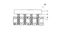
- the interposer 200 and the connection pads 41 of the semiconductor chip 11 are mounted via the solder 40 to form a semiconductor device 301 as shown in FIG.
- the connection pads 41 of the semiconductor chip 11 have corresponding conductive vias 9, and a part of the insulating resin layer 7 stacked on the conductive vias 9 is removed to form solder.
- a method similar to the method of forming the connection via 24 can be used.
- FIG. 26 is a schematic sectional view showing the structure of an interposer 201 according to the third embodiment of the present invention.
- the basic structure of the interposer 201 according to the third embodiment is the same as that of the interposer 200 according to the second embodiment.
- the base material 1 is used as a starting material for the process, and the insulating resin layer 7 is formed after the through electrode 3 is formed.
- this embodiment is an example in the case of forming the base material 30 with the insulating resin layer in which the insulating resin layer 7 is formed on the surface of the base material 1 as a starting material.
- the CTE of the insulating resin layer 7 is desirably in the range of 30 to 40.
- the interposer 201 in this embodiment is manufactured in the order of through-hole formation, embedded resin layer formation, connection hole formation, and through-electrode / wiring layer formation.
- the through hole 13 is formed as shown in FIG.
- an excimer laser, a UV-YAG laser, or a CO 2 laser can be selected for forming the through hole 13.
- the through-hole 13 is filled with the embedded resin layer 16 by, for example, screen printing.
- the CTE of the embedded resin layer 16 is desirably about 30 to 40, and it is more preferable that the difference from the insulating resin layer 7 is small.
- the central portion of the embedded resin layer 16 is irradiated with a laser to remove a portion of the embedded resin layer 16.
- the connection hole 17 optimal for electrode formation can be formed.
- the insulating resin layer 7 and the embedded resin layer 16 are roughened, and then the seed layer 14 is formed by electroless plating, as shown in FIG. 28 (f). Then, a pattern is formed by the resist 15.
- the base material 30 with an insulating resin layer is used as the base material 1, the base material 1 and the plating do not come into contact with each other no matter what pattern is formed. Can be increased.
- the through hole 3 is formed by filling the connection hole 17 and the opening of the resist 15 with a conductive material. Conductive vias 9 directly connected to the lands 6 on both end faces of the through electrode 3 are formed simultaneously.
- FIG. 28 (g) After removing the resist 15, the seed layer 14 is removed by etching, and the through electrode 3 and the wiring layer 8 are formed as shown in FIG. 28 (h).
- FIG. 28H which is a cross-sectional view, the through electrode 3 and the wiring layer 8 are shown apart from each other, but are electrically connected.
- FIG. 25 (k) is shown as a cross-sectional view in FIG.
- the interposer (glass interposer) 201 shown in FIG. 26 is manufactured.
- an interposer with high heat resistance and high reliability can be obtained.
- the starting material is the base material 30 with an insulating resin layer
- the through electrode 3 and the wiring layer 8 can be formed simultaneously, and the front and back of the interposer 201 can be formed without forming the conductive via 9.
- the wiring layer 8 can be connected, and the process can be shortened.
- a method suitable for the size of the wiring to be formed can be selected as appropriate.
- the build-up method is used to form the fine wiring layer 8, and the interposers 200 and 201 are manufactured using the conventional method of laminating a prepreg and a copper foil for the wiring layer 8 whose wiring size is not fine. It is also possible to do.
- the semiconductor chip 11 is mounted on the interposer 201 to form a semiconductor device 302 as shown in FIG.
- the base material 1 is used.
- the liquid of the dissolved insulating resin layer 7 is impregnated and dried to form an insulating resin layer (embedded resin layer 16 and insulating resin layer 7) on the surface of the base material 1 and the through hole 13. May be.
- only one wiring layer 8 is provided.
- the wiring layers 8 and the insulating resin layers 7 and connecting them with the conductive vias 9, FIG. 28 and FIG. It is also possible to manufacture an interposer in which a plurality of wiring layers 8 as shown in FIG.
- Example 2-1 of the present invention corresponds to the manufacturing method (FIG. 23) according to the second embodiment.
- Example 2-1 First, Sanei Chemical Co., Ltd. is applied to a glass substrate 1 (see FIG. 25A) in which a through hole 13 having an opening diameter of 70 ⁇ m is formed in a low expansion glass substrate (thickness 300 ⁇ m, CTE: 3.5). After inserting the hole filling resin (CTE40) made by screen printing, the embedded resin layer 16 was smoothed by buffing (see FIG. 25B). Next, by irradiating the formed embedded resin layer 16 with UV-YAG laser, a connection hole 17 having an opening diameter of 50 ⁇ m was formed. Thereafter, desmearing was performed to roughen the resin. Thereafter, the seed layer 14 was formed by electroless plating (see FIG. 25D).
- a dry film resist RY-3525 (thickness 25 ⁇ m) manufactured by Hitachi Chemical Co., Ltd. was laminated on both surfaces of the obtained glass substrate 1. Thereafter, an opening was formed by photolithography so that the opening diameter was smaller than the connection hole 17 and the bottom surface of the opening did not contact the glass. Then, the penetration electrode 3 which consists of the connection electrode 22 in the connection hole 17 and the land 6 on the upper and lower sides was formed by electrolytic copper plating (refer FIG.25 (f)). Next, after removing the resist 15 (see FIG. 25 (g)), GX-T31 (thickness 15 ⁇ m) manufactured by Ajinomoto Fine Techno Co., Ltd. was thermocompression bonded to the surface of the glass substrate 1 (see FIG. 25 (h)). Thereafter, a connection via 24 was formed immediately above the land 6 by a UV-YAG laser (see FIG. 25 (i)).
- the seed layer 14 was formed by electroless plating. After that, a resist pattern was formed by photolithography, and electrolytic plating, resist peeling, and flash etching processes were performed to obtain an interposer 200 using the glass substrate 1 having the through electrodes 3 (see FIG. 25 (j)). ).
- Example 2-2 of the present invention corresponds to the manufacturing method (FIG. 26) according to the third embodiment.
- Example 2-2 First, GX-T31 (thickness 15 ⁇ m) manufactured by Ajinomoto Fine Techno Co., Ltd. was thermocompression bonded to both surfaces of a low expansion glass substrate (thickness 300 ⁇ m, CTE: 3.5) (FIG. 28A). reference).
- the glass substrate 1 was irradiated with a UV-YAG laser, thereby forming a through hole 13 having an opening with a diameter of 70 ⁇ m (see FIG. 28B).
- a hole filling resin (CTE40) manufactured by Yamaei Chemical Co., Ltd. was inserted by screen printing, and the embedded resin layer 16 was smoothed by buffing (see FIG. 28C).
- a connection hole 17 having an opening diameter of 50 ⁇ m was formed.
- desmearing was performed to roughen the resin.
- the seed layer 14 was formed by electroless plating (see FIGS. 28D and 28E).
- a dry film resist RY-3525 (thickness 25 ⁇ m) manufactured by Hitachi Chemical Co., Ltd. was laminated on both surfaces of the obtained glass substrate 1. After that, an opening having an opening diameter smaller than the connection hole 17 is formed by photolithography, and then the through electrode 3 including the connection electrode 22 and the lands 6 above and below it is formed by electrolytic copper plating, and the wiring layer 8 is formed. (See FIGS. 28 (f) and 28 (g)). Next, resist stripping and flash etching steps were performed to obtain an interposer 201 using the glass substrate 1 having the through electrodes 3 (see FIG. 28H).
- the interposers 200 and 201, the semiconductor devices 301 and 302, and the manufacturing methods thereof according to the second and third embodiments can solve the problems of the present application and the problems described later. Can also be solved. The details of the problem will be described below.
- CMOS complementary metal-oxide-semiconductor
- CPU complementary metal-oxide-semiconductor
- the pitch of the connection terminals and the pitch of the connection portion on the printed wiring board side to be electrically connected to the semiconductor element differ from each other by several to several tens of times. Therefore, when the semiconductor element and the printed wiring board are to be electrically connected, an intermediary board (semiconductor element mounting board) for pitch conversion called an interposer is used.
- an intermediary board semiconductor element mounting board for pitch conversion called an interposer is used.
- a semiconductor element is mounted on one surface of an interposer and connected to a printed wiring board on the other surface or the periphery of the substrate.
- a substrate using an organic material has been used as an interposer for mounting a semiconductor element on a printed wiring board.
- electronic devices represented by recent smartphones, there is a three-dimensional or 2.5-dimensional mounting technology in which semiconductor elements are stacked vertically or different types of semiconductor elements are mounted side by side on the same substrate. It is becoming essential.
- the interposer is also required to create finer wiring.
- the conventional organic substrate has a problem that it is difficult to form a fine wiring with a scale because the moisture absorption of the resin and the expansion and contraction due to temperature are large.
- TSV Through-Silicon Via
- TGV Through-Glass Via
- the silicon interposer (Si-IP) is superior to the glass interposer (G-IP) in fine workability, and the wiring / TSV formation process has already been established.
- the peripheral portion of the wafer cannot be used, and since it cannot be produced in a large size at a time, there is a disadvantage that the cost is increased.
- G-IP is capable of batch processing with a large panel, and a roll-to-roll production method is also conceivable, which can greatly reduce costs.
- TSV digs holes by gas etching, which increases the processing time and includes a wafer thinning process. It is a factor.
- G-IP is superior in electrical characteristics because there is no fear of generation of parasitic elements even in a high-speed circuit because the substrate itself is an insulator unlike Si-IP.
- the process of forming the insulating film itself is not necessary, so that the insulation reliability is high and the tact time is short.
- an interposer can be made at a low cost.
- a process for forming fine wiring and TGV has not been established yet, and copper which is the mainstream of wiring materials can be used.
- Examples include poor glass adhesion.
- an inorganic adhesion layer is formed on the glass surface and a wiring layer and a through electrode are formed thereon in order to improve the adhesion of the wiring layer.
- the adhesion between the glass and the wiring layer at room temperature is ensured, but the difference in thermal expansion coefficient between the glass and the conductive layer is large, a thermal stress is generated in the temperature cycle, and the glass substrate and the conductive layer are separated. The electrical connection is damaged.
- many of these inorganic adhesion layers have conductivity, and when forming a wiring layer, it is necessary to etch the adhesion layer in addition to the etching of copper, resulting in an increase in cost.
- the conductive layer is formed in the through hole 13 of the base material 1.
- the conductive layer 5 in the connection hole 17 is filled with the embedded resin layer 16 having good adhesion with the substrate 5 and having an expansion coefficient larger than that of the base material 1 and smaller than that of the conductive layer 5, and opened in the center side of the embedded resin layer 16.
- the front and back wiring layers 8 are electrically connected through the formed conductive vias 9.
- the base material 1 made of glass or the like and the conductive layer 5 do not contact each other, and the thermal stress due to heating can be relaxed. Therefore, according to the interposers 200 and 201 according to one embodiment of the present invention, the conductive layer 5 is hardly peeled off, and an interposer with high electrical connection reliability can be provided. Further, according to one embodiment of the present invention, it is possible to provide a method for manufacturing the interposers 200 and 201, semiconductor devices 301 and 302 including the interposers 200 and 201, and a method for manufacturing the semiconductor devices 301 and 302.
- the interposer and the semiconductor device according to the present invention may be manufactured by combining the configurations described in the embodiments.
- the interposer and the semiconductor device according to the present invention may be manufactured by combining the first embodiment and the second embodiment.
- other embodiments of the invention will be apparent to those skilled in the art by reference to the description of the invention. Therefore, it is to be understood that the claims encompass these modifications and embodiments that fall within the scope and spirit of the present invention.
- the present invention relates to an interposer and a semiconductor device, and in particular, can be used for an interposer interposed between a package substrate and an IC chip and a semiconductor device including an interposer for connecting an IC chip.
Landscapes
- Production Of Multi-Layered Print Wiring Board (AREA)
- Physics & Mathematics (AREA)
- Geometry (AREA)
- Printing Elements For Providing Electric Connections Between Printed Circuits (AREA)
Abstract
熱膨張、熱収縮による導電層パターンの剥離を防止することで充分な信頼性を有することが可能な、インターポーザ、半導体装置、インターポーザの製造方法、半導体装置の製造方法を提供する。本発明に係るインターポーザ(100)は、貫通孔を持つ基材(1)と、基材(1)表面に形成され、且つ導通ビア(9)を有する絶縁性樹脂層(7)と、基材(1)上に絶縁性樹脂層(7)を介在して配置された配線層(8)と、貫通孔(13)の側面にのみ形成された無機密着層(4)と、無機密着層(4)で貫通孔内に形成される接続孔に充填されて基材(1)の両面側を導通可能な貫通電極(3)と、を備え、貫通電極(3)は、導通ビア(9)を介して配線層(8)と電気的に接続され、無機密着層(4)の熱膨張率は、基材(1)の熱膨張率よりも大きく、且つ貫通電極(3)の熱膨張率よりも小さい。
Description
本発明は、インターポーザ、半導体装置、インターポーザの製造方法、半導体装置の製造方法に関する。
インターポーザは、例えば、パッケージ基板とICチップとの間に配置されて使用される部品である。そして、パッケージ基板とICチップとの間にインターポーザを介在させる技術としては、例えば、特許文献1から特許文献4に記載されたものがある。
しかしながら、インターポーザ、特にガラスを基材とするガラスインターポーザを製造するにあたり、いくつかの克服すべき課題も多い。
その課題の一つに、基材であるガラスと、導電層パターン(例えば、貫通電極)に用いられる銅等との熱膨張率の差が大きく、また、弾性率も大きいことに対して、銅等とガラスとの密着強度が充分ではないため、実装時の高温プロセスや信頼性試験の温度サイクル等により、銅等からなる導電層パターンが、ガラス表面から剥離してしまうという現象が挙げられる。
本発明は、このような問題点を解決しようとするものであり、熱膨張、熱収縮による導電層パターンの剥離を防止することで充分な信頼性を有することが可能な、インターポーザ、半導体装置、インターポーザの製造方法、半導体装置の製造方法を提供することを目的とする。
その課題の一つに、基材であるガラスと、導電層パターン(例えば、貫通電極)に用いられる銅等との熱膨張率の差が大きく、また、弾性率も大きいことに対して、銅等とガラスとの密着強度が充分ではないため、実装時の高温プロセスや信頼性試験の温度サイクル等により、銅等からなる導電層パターンが、ガラス表面から剥離してしまうという現象が挙げられる。
本発明は、このような問題点を解決しようとするものであり、熱膨張、熱収縮による導電層パターンの剥離を防止することで充分な信頼性を有することが可能な、インターポーザ、半導体装置、インターポーザの製造方法、半導体装置の製造方法を提供することを目的とする。
本発明の一態様は、貫通孔を持つ基材と、
前記基材表面に1層以上形成され、且つ導通ビアを有する絶縁性樹脂層と、
前記基材上に前記絶縁性樹脂層を介在して配置された1層以上の配線層と、
前記貫通孔の側面にのみ形成された無機密着層と、
前記無機密着層で前記貫通孔内に形成される接続孔に充填されて前記基材の両面側を導通可能な貫通電極と、を備え、
前記貫通電極は、前記導通ビアを介して前記配線層と電気的に接続され、
前記無機密着層の熱膨張率は、前記基材の熱膨張率よりも大きく、且つ前記貫通電極の熱膨張率よりも小さいことを特徴とするインターポーザである。
前記基材表面に1層以上形成され、且つ導通ビアを有する絶縁性樹脂層と、
前記基材上に前記絶縁性樹脂層を介在して配置された1層以上の配線層と、
前記貫通孔の側面にのみ形成された無機密着層と、
前記無機密着層で前記貫通孔内に形成される接続孔に充填されて前記基材の両面側を導通可能な貫通電極と、を備え、
前記貫通電極は、前記導通ビアを介して前記配線層と電気的に接続され、
前記無機密着層の熱膨張率は、前記基材の熱膨張率よりも大きく、且つ前記貫通電極の熱膨張率よりも小さいことを特徴とするインターポーザである。
本発明の一態様であれば、熱膨張、熱収縮による導電層パターン(例えば、貫通電極)の剥離を防止することで充分な信頼性を有することが可能な、インターポーザを提供することが可能となる。また、本発明の一態様であれば、そのインターポーザの製造方法、そのインターポーザを備えた半導体装置及びその半導体装置の製造方法を提供することが可能となる。
以下、本発明の各実施形態について、図面を参照しつつ説明する。なお、以下の詳細な説明では、本発明の各実施形態の完全な理解を提供するように多くの特定の細部について記載される。しかしながら、かかる特定の細部がなくても1つ以上の実施形態が実施できることは明らかであろう。また、各図において、同様又は類似した機能を発揮する構成要素には同一の参照符号を付し、重複する説明は省略する。
(第1実施形態)
以下、本発明の第1実施形態について、図面を参照しつつ説明する。
(インターポーザ100の構成)
図1中に示すように、インターポーザ100は、基材1と、貫通電極3と、無機密着層4と、ランド6と、絶縁性樹脂層7と、配線層8と、導通ビア9を備えている。基材1の表面にも無機密着層4を備えていても良い。また、この無機密着層4の上に導電層5(導電層パターン)を備えていても良い。
基材1は、SiO2を主成分とする、ガラスからなる基板(ガラス基材)であり、貫通孔13を有している。
また、基材1の熱膨張率は、低膨張ガラスで3~4ppm/℃、ソーダガラスで8~9ppm/℃であり、製造方法や、Na等の金属成分の添加により、3~9ppm/℃の制御が可能である。なお、熱膨張率は、JIS:R3102やJIS:K7197に従い、TMA(熱機械分析)にて測定した。
また、基材1に貫通孔13を形成する方法としては、例えば、CO2レーザやUVレーザ、ピコ秒レーザやフェムト秒レーザ、エキシマレーザや放電加工、感光性ガラスやブラスト加工等を使用可能であり、基材1の厚さや貫通孔13の孔径で選択すれば良い。
貫通電極3は、導電性材料で形成されており、貫通孔13内に配置されている。
貫通電極3を形成する導電性材料としては、例えば、銅、銀、金、ニッケル、白金、パラジウム、ルテニウム、錫、錫銀、錫銀銅、錫銅、錫ビスマス、錫鉛のうちいずれかの単体金属、または、いずれかの単体金属の積層や化合物が使用可能であり、無機密着層4との密着性や、電気的に接続安定性の高い材料を選定すれば良い。
また、貫通電極3を形成する導電性材料としては、例えば、上述した材料のうち少なくとも一つの金属粉と樹脂材料との混合物である導電性ペーストも使用可能である。
また、貫通電極3を形成する方法としては、特に規定しないが、無電解めっき法や電解めっき法を用いることが可能である。
貫通電極3を形成する導電性材料としては、例えば、銅、銀、金、ニッケル、白金、パラジウム、ルテニウム、錫、錫銀、錫銀銅、錫銅、錫ビスマス、錫鉛のうちいずれかの単体金属、または、いずれかの単体金属の積層や化合物が使用可能であり、無機密着層4との密着性や、電気的に接続安定性の高い材料を選定すれば良い。
また、貫通電極3を形成する導電性材料としては、例えば、上述した材料のうち少なくとも一つの金属粉と樹脂材料との混合物である導電性ペーストも使用可能である。
また、貫通電極3を形成する方法としては、特に規定しないが、無電解めっき法や電解めっき法を用いることが可能である。
なお、めっき法で形成する貫通電極3の形態としては、コンフォーマルめっき形態やフィルドめっき形態がある。コンフォーマルめっき形態では、貫通孔13の中央にスルーホール状の孔が残っており、絶縁性樹脂や導電性ペーストをスクリーン印刷法で充填すれば良い。ここで、導電性ペーストで充填する場合は、コンフォーマルめっき皮膜とともにランド6とし、導通ビア9と導通を確保することが可能である。また、導電性ペーストの表面に無電解めっき層や電解めっき層を導電層5として形成し、さらに、コンフォーマルめっき皮膜との導通性を向上させてランド6とし、導通ビア9と導通を確保することも可能である。一方、絶縁性樹脂で充填する場合は、絶縁性樹脂の表面に無電解めっき層や電解めっき層を形成して、コンフォーマルめっき皮膜との導通性を確保してランド6とし、導通ビア9と導通を確保すれば良い。
また、貫通電極3を形成する方法としては、例えば、無機密着層4を形成した後に、導電性ペーストをスクリーン印刷法で充填して、貫通電極3とする方法を用いることも可能である。
なお、導電性材料として多く使用される銅の熱膨張率は、16ppm/℃程度である。
無機密着層4は、基材1の両面と貫通孔13内に形成されている。また、無機密着層4のうち、貫通孔13内に形成されている部分は、貫通電極3と貫通孔13の内壁面(内径面)との間に配置されている。
なお、導電性材料として多く使用される銅の熱膨張率は、16ppm/℃程度である。
無機密着層4は、基材1の両面と貫通孔13内に形成されている。また、無機密着層4のうち、貫通孔13内に形成されている部分は、貫通電極3と貫通孔13の内壁面(内径面)との間に配置されている。
また、無機密着層4の材料としては、例えば、基材1と導電性材料との密着性が高く、且つ熱膨張率が基材1より高い材料である、酸化錫、酸化インジウム、酸化亜鉛、ニッケル(熱膨張率:15ppm/℃)、ニッケルリン、クロム(熱膨張率:8ppm/℃)、酸化クロム、チッ化アルミ、酸化アルミ、タンタル(熱膨張率:6ppm/℃)、チタン(熱膨張率:9ppm/℃)、銅(熱膨張率:16ppm/℃)等の材料が使用可能である。これにより、基材1と、貫通電極3及び基材1の表面に形成されている導電層5との間の密着力を向上させることが可能となる。これに加え、無機密着層4が基材1に比べて熱膨張率が高いことで、貫通電極3及び導電層5と基材1の線膨張係数の差によって発生する、層間にかかる応力を低減することが可能となる。
また、無機密着層4の熱膨張率の上限は、導電性材料の熱膨張率の上限よりも低いことが望ましい。
また、無機密着層4の材料として、上述した密着力の高い材料を使用することにより、導電性材料と基材1の熱膨張率の差によって発生する、層間にかかる応力を低減して、導電性材料の剥離を回避することが可能となる。
また、無機密着層4は、上記の材料を、単体、または、ITO膜(熱膨張率:9ppm/℃)のように、二種類以上の複合材料を単層にて使用することが可能である。また、無機密着層4は、クロム/銅、チタン/銅のように、二種類以上の複合材料を2層以上の積層膜にて使用することが可能である。
また、無機密着層4の材料として、上述した密着力の高い材料を使用することにより、導電性材料と基材1の熱膨張率の差によって発生する、層間にかかる応力を低減して、導電性材料の剥離を回避することが可能となる。
また、無機密着層4は、上記の材料を、単体、または、ITO膜(熱膨張率:9ppm/℃)のように、二種類以上の複合材料を単層にて使用することが可能である。また、無機密着層4は、クロム/銅、チタン/銅のように、二種類以上の複合材料を2層以上の積層膜にて使用することが可能である。
また、無機密着層4の膜厚は特に規定しないが、0.1μm以上1μm以下の範囲内であれば、基材1との密着性と、熱膨張率の差を緩和する効果を得ることが可能である。
また、無機密着層4の形成方法は特に規定しないが、スパッタ成膜法、無電解めっき法等を用いることが可能である。
導電層5は、導電性材料で形成されており、無機密着層4を介して、基材1の両面に配置されていても良い。
導電層5を形成する導電性材料としては、例えば、銅、銀、金、ニッケル、白金、パラジウム、ルテニウム、錫、錫銀、錫銀銅、錫銅、錫ビスマス、錫鉛のうちいずれかの単体金属、または、いずれかの単体金属の積層や化合物が使用可能であり、無機密着層4との密着性や、電気的に接続安定性の高い材料を選定すれば良い。
また、無機密着層4の形成方法は特に規定しないが、スパッタ成膜法、無電解めっき法等を用いることが可能である。
導電層5は、導電性材料で形成されており、無機密着層4を介して、基材1の両面に配置されていても良い。
導電層5を形成する導電性材料としては、例えば、銅、銀、金、ニッケル、白金、パラジウム、ルテニウム、錫、錫銀、錫銀銅、錫銅、錫ビスマス、錫鉛のうちいずれかの単体金属、または、いずれかの単体金属の積層や化合物が使用可能であり、無機密着層4との密着性や、電気的に接続安定性の高い材料を選定すれば良い。
また、導電層5を形成する導電性材料としては、例えば、上述した材料のうち少なくとも一つの金属粉と樹脂材料との混合物である導電性ペーストも使用可能である。
また、導電層5を形成する方法としては、特に規定しないが、無電解めっき法や電解めっき法を用いることが可能である。
ランド6は、導電層5を挟んで貫通電極3の上下端に形成されていても良い。
ランド6の形状は、例えば、基材1の表面と同じ高さで形成する形状や、基材1の表面よりも数ミクロン高く形成する形状とすることが可能である。
また、ランド6を形成する方法としては、特に規定しないが、貫通孔13の内部を導電性材料や絶縁性樹脂で充填した後、導電層5や、貫通孔13内に充填した樹脂を基材1の表面まで研磨除去して貫通電極3の上下端を露出させてランド6とする工法や、貫通電極3の上下端に位置する導電層5をパターニングしてランド6とする工法を用いることが可能である。
また、ランド6を形成する方法としては、例えば、貫通孔13の両端をランド6の形状に削り、導電性材料を充填する工法を用いることが可能である。この場合、ランド6に接する部分以外の無機密着層4は、研磨、または、パターニングの際のエッチング処理により除去するものとする。
なお、貫通電極3をフィルドめっき形態で形成した場合、貫通電極3上にそのままスタック形成して、ランド6を形成することが可能である。
ランド6の外径は、貫通孔13の内径と同じとする。なお、ランド6の外径は、導通ビア9の形成の加工精度を加味して、貫通孔13の内径よりも大きしてもよい。この場合、加工精度の変動要因として、基材1の伸縮、ビア孔の加工方式の位置精度バラツキなどが挙げられ、ランド6の外径の上限として、貫通孔13の内径よりも20μmまで大きくすれば、ランド6より導通ビア9が脱落することなく、良好な導通性を得ることが可能となる。
なお、貫通電極3をフィルドめっき形態で形成した場合、貫通電極3上にそのままスタック形成して、ランド6を形成することが可能である。
ランド6の外径は、貫通孔13の内径と同じとする。なお、ランド6の外径は、導通ビア9の形成の加工精度を加味して、貫通孔13の内径よりも大きしてもよい。この場合、加工精度の変動要因として、基材1の伸縮、ビア孔の加工方式の位置精度バラツキなどが挙げられ、ランド6の外径の上限として、貫通孔13の内径よりも20μmまで大きくすれば、ランド6より導通ビア9が脱落することなく、良好な導通性を得ることが可能となる。
絶縁性樹脂層7は、1層以上積層され、もっとも基材1に近いものは、基材1あるいは、導電層5上に形成されている。
また、絶縁性樹脂層7は、必要な層数が積層されている。なお、絶縁性樹脂層7の層数は、例えば、製品の設計により設定すれば良い。
また、絶縁性樹脂層7の材料としては、エポキシ/フェノール系樹脂、ポリイミド樹脂、シクロオレフィン、PBO樹脂のうちいずれか一つの材料、または、少なくとも二つの材料を組み合わせた複合材料を用いることが可能である。
この場合、例えば、絶縁性樹脂層7の材料を、熱膨張率が30~100ppm/℃と導電性材料よりも高く、かつ弾性率が高い材料とすることにより、導電層5がある場合には、この導電層5を覆うことで導電層5と基材1との層間にかかる応力を減少させて、導電層5の剥離を抑制する効果を付与することが可能となる。
また、絶縁性樹脂層7の材料としては、例えば、ドライフィルムや液レジが使用可能であり、特に規定するものではない。
配線層8は、絶縁性樹脂層7上、あるいは隣接する絶縁性樹脂層同士に挟まれるように形成されている。
また、配線層8は、必要な層数が積層されている。なお、配線層8の層数は、例えば、製品の設計により設定すれば良い。
また、配線層8の形成方法は特に規定しないが、例えば、無電解めっき、または、スパッタ膜をシード層として、電解めっきにて厚付けし、セミアディティブ法やサブトラクティブ法によりパターン形成する方法を用いてもよい。
配線層8は、絶縁性樹脂層7上、あるいは隣接する絶縁性樹脂層同士に挟まれるように形成されている。
また、配線層8は、必要な層数が積層されている。なお、配線層8の層数は、例えば、製品の設計により設定すれば良い。
また、配線層8の形成方法は特に規定しないが、例えば、無電解めっき、または、スパッタ膜をシード層として、電解めっきにて厚付けし、セミアディティブ法やサブトラクティブ法によりパターン形成する方法を用いてもよい。
導通ビア9は、絶縁性樹脂層7に形成されており、導電層5と配線層8を、電気的に接続させている。
また、導通ビア9の基材1側の径(ボトムの径)は、貫通孔13及び貫通電極3の径よりも小さくする。これにより、スタックド構造で導通ビア9を積層することが可能になり、絶縁性樹脂層7上の配線層8とランド6を形成する上で、ランド6間に配置可能な配線本数を増やすことが可能になると共に、基材1に形成する貫通孔13の孔ピッチを狭く形成することが可能になる。
また、導通ビア9は、絶縁性樹脂層7に形成したビア孔内に、コンフォーマルめっき等、導電性材料を充填する加工を行って形成する。
また、導通ビア9の基材1側の径(ボトムの径)は、貫通孔13及び貫通電極3の径よりも小さくする。これにより、スタックド構造で導通ビア9を積層することが可能になり、絶縁性樹脂層7上の配線層8とランド6を形成する上で、ランド6間に配置可能な配線本数を増やすことが可能になると共に、基材1に形成する貫通孔13の孔ピッチを狭く形成することが可能になる。
また、導通ビア9は、絶縁性樹脂層7に形成したビア孔内に、コンフォーマルめっき等、導電性材料を充填する加工を行って形成する。
絶縁性樹脂層7にビア孔を形成する方法は、例えば、絶縁性樹脂層7の材料により選択すれば良く、絶縁性樹脂層7の材料が熱硬化性樹脂であれば、例えば、CO2レーザやUVレーザ等が用いた加工により形成可能であり、レーザ加工の後は、例えば、レーザ加工で発生したスミアを除去するためにデスミア処理を行えば良い。また、絶縁性樹脂層7の材料が感光性レジストの場合は、例えば、フォトリソ法にて形成すれば良い。
以上により、本実施形態のインターポーザ100は、多層構造の貫通電極付きインターポーザである。また、本実施形態のインターポーザ100であれば、基材1の両面に形成した配線層8の間で、高い導通信頼性を実現することが可能となる。
なお、図1中に示す絶縁性樹脂層7及び配線層8の必要層数や、導通パッド部の金属層の形状や高さは、一例であり、特に規定するものではない。
以上により、本実施形態のインターポーザ100は、多層構造の貫通電極付きインターポーザである。また、本実施形態のインターポーザ100であれば、基材1の両面に形成した配線層8の間で、高い導通信頼性を実現することが可能となる。
なお、図1中に示す絶縁性樹脂層7及び配線層8の必要層数や、導通パッド部の金属層の形状や高さは、一例であり、特に規定するものではない。
(半導体装置300の構成)
図2中に示すように、半導体装置300は、インターポーザ100と、半導体素子11を備えている。
インターポーザ100は、はんだボール18を用いて、図示しないプリント配線基板に搭載される。
半導体素子11は、はんだボール(図示せず)を用いて、インターポーザ100の片面(図2中では、上側の面)に搭載される。
なお、図2中に示す半導体素子11の形状や、半導体素子11とインターポーザ100との接続方式は、一例であり、特に規定するものではない。
以上により、本実施形態の半導体装置300であれば、接続対象である半導体素子11やインターポーザ100との間で導通パッドの材料を最適化することで、高い接続強度を得るとともに、実装時の熱変形の最適化により、高い接続信頼性を実現することが可能となる。
(第1実施例)
以下、本発明の第1実施例について、インターポーザ100の製造方法と、半導体装置300の製造方法を含めて説明する。
(実施例1-1)
以下、本発明の実施例1-1について、図1及び図2を参照しつつ、図3から図8を用いて説明する。
基材1として、厚さが0.3mm、大きさが200mm×200mm、熱膨張率が4ppm/℃の低膨張ガラスを用いた。
無機密着層4を、スパッタにて、0.1μm厚のCr膜(熱膨張率:8ppm/℃)と、0.2μm厚のCu膜とを積層して形成した。
また、電解銅めっき層2(熱膨張率:16ppm/℃)を、導電性材料を用いて形成した。また、貫通電極3を、フィルド銅めっき構成で形成した。
以下、本発明の第1実施例について、インターポーザ100の製造方法と、半導体装置300の製造方法を含めて説明する。
(実施例1-1)
以下、本発明の実施例1-1について、図1及び図2を参照しつつ、図3から図8を用いて説明する。
基材1として、厚さが0.3mm、大きさが200mm×200mm、熱膨張率が4ppm/℃の低膨張ガラスを用いた。
無機密着層4を、スパッタにて、0.1μm厚のCr膜(熱膨張率:8ppm/℃)と、0.2μm厚のCu膜とを積層して形成した。
また、電解銅めっき層2(熱膨張率:16ppm/℃)を、導電性材料を用いて形成した。また、貫通電極3を、フィルド銅めっき構成で形成した。
絶縁性樹脂層7の材料には、エポキシ系樹脂からなるABFを使用した。
配線層8の材料には、シード層に無電解銅めっきを使用し、電解銅めっきの厚さを8μmとし、配線層8のLS値を10μmとし、セミアディティブ法により形成した。
導通ビア9は、コンフォーマルめっきにて形成した。絶縁性樹脂層7への導通ビア9の形成には、UV-YAGレーザを使用した。
基材1への貫通孔13の形成には、ピコ秒レーザを使用した。貫通孔13と導通ビア9の内径は、50μmφとした。
配線層8の材料には、シード層に無電解銅めっきを使用し、電解銅めっきの厚さを8μmとし、配線層8のLS値を10μmとし、セミアディティブ法により形成した。
導通ビア9は、コンフォーマルめっきにて形成した。絶縁性樹脂層7への導通ビア9の形成には、UV-YAGレーザを使用した。
基材1への貫通孔13の形成には、ピコ秒レーザを使用した。貫通孔13と導通ビア9の内径は、50μmφとした。
実施例1-1に係るインターポーザ100の製造方法としては、貫通孔形成工程と、無機密着層形成工程と、導電層・貫通電極形成工程と、不要層除去工程と、絶縁性樹脂層形成工程と、ビア孔形成工程と、導通ビア・配線層形成工程を含む方法を用いた。
以下、これらの工程の詳細について説明する。
まず、貫通孔形成工程では、図3中に示すように、基材1に対し、ピコ秒レーザにて貫通孔13を形成した。
以下、これらの工程の詳細について説明する。
まず、貫通孔形成工程では、図3中に示すように、基材1に対し、ピコ秒レーザにて貫通孔13を形成した。
次の無機密着層形成工程では、図4中に示すように、基材1の両面に対し、スパッタCr膜とスパッタCu膜とを連続して成膜し、基材1の表面と貫通孔13内に、無機密着層4を形成した。
次の導電層・貫通電極形成工程では、図5中に示すように、基材1の両面に対し、無機密着層4の上に、導電性材料を用いて電解銅めっき層2を形成した。これに加え、貫通孔13内に銅めっきを充填したフィルドめっき構成により、貫通孔13内に貫通電極3を形成した。
次の不要層除去工程では、図6中に示すように、基材1の両面に形成した電解銅めっき層2を、ケミカルポリッシュで除去し、さらに、無機密着層4のCrスパッタ膜を硝酸セリウムアンモニウム水溶液にてエッチング除去して、基材1に貫通電極3を配置したコア基板10を形成した。
次の導電層・貫通電極形成工程では、図5中に示すように、基材1の両面に対し、無機密着層4の上に、導電性材料を用いて電解銅めっき層2を形成した。これに加え、貫通孔13内に銅めっきを充填したフィルドめっき構成により、貫通孔13内に貫通電極3を形成した。
次の不要層除去工程では、図6中に示すように、基材1の両面に形成した電解銅めっき層2を、ケミカルポリッシュで除去し、さらに、無機密着層4のCrスパッタ膜を硝酸セリウムアンモニウム水溶液にてエッチング除去して、基材1に貫通電極3を配置したコア基板10を形成した。
次の絶縁性樹脂層形成工程及びビア孔形成工程では、図7中に示すように、コア基板10の両面に絶縁性樹脂をラミネートして絶縁性樹脂層7を形成し、貫通電極3上の絶縁性樹脂層7にUV-YAGレーザにてビア孔24を形成した。ここで、ビア孔24の径は、貫通電極3の径よりも小径とした。また、UV-YAGレーザ加工にて生じたビア孔24内の塵を、アルカリ水溶液系の処理液でデスミアしてクリーニングした。
次の導通ビア・配線層形成工程では、絶縁性樹脂層7の上に、シード層として無電解銅めっきを形成した。さらに、シード層の上へ、図8中に示すように、ネガ形レジストにて配線層部と導通ビア部(共に図示せず)が開口したレジストパターンを形成し、セミアディティブ法により、導電性材料として電解銅めっきを8μm厚で形成した。その後、レジスト及び不要部分のシード層を除去して、配線層8と導通ビア9とを形成した。
次の導通ビア・配線層形成工程では、絶縁性樹脂層7の上に、シード層として無電解銅めっきを形成した。さらに、シード層の上へ、図8中に示すように、ネガ形レジストにて配線層部と導通ビア部(共に図示せず)が開口したレジストパターンを形成し、セミアディティブ法により、導電性材料として電解銅めっきを8μm厚で形成した。その後、レジスト及び不要部分のシード層を除去して、配線層8と導通ビア9とを形成した。
また、実施例1-1に係る半導体装置300の製造方法としては、上述したインターポーザ100の製造方法で製造されたインターポーザ100に、導通パッドを形成する導通パッド形成工程と、導通パッド上に半導体素子11を固定する半導体素子固定工程を含む方法を用いた。
まず、導通パッド形成工程では、図8中に示すように、基材1へ感光性のソルダーレジスト12を積層して露光及び現像を行い、Ni/Auめっきにて導通パッド部(図示せず)を形成した。
次の半導体素子固定工程では、はんだにより、導通パッド上に半導体素子11を固定した。
なお、実施例1-1では、片面の配線層8の層数を2層とし、表面の被覆層をソルダーレジスト12とし、導通パッド表面の表面処理をNi/Auとしたが、これらの構成は、特に限定するものではない。
まず、導通パッド形成工程では、図8中に示すように、基材1へ感光性のソルダーレジスト12を積層して露光及び現像を行い、Ni/Auめっきにて導通パッド部(図示せず)を形成した。
次の半導体素子固定工程では、はんだにより、導通パッド上に半導体素子11を固定した。
なお、実施例1-1では、片面の配線層8の層数を2層とし、表面の被覆層をソルダーレジスト12とし、導通パッド表面の表面処理をNi/Auとしたが、これらの構成は、特に限定するものではない。
(実施例1-2)
以下、本発明の実施例1-2について、図1から図8を参照しつつ、図9から図15を用いて説明する。
基材1として、厚さが0.3mm、大きさが200mm×200mm、熱膨張率が4ppm/℃の低膨張ガラスを用いた。
無機密着層4を、スパッタにて、0.1μm厚のCr膜(熱膨張率:8ppm/℃)と、0.2μm厚のCu膜とを積層して形成した。
また、電解銅めっき層2(熱膨張率:16ppm/℃)を、導電性材料を用いて形成した。また、貫通電極3を、コンフォーマル銅めっき構成で形成した。また、導電層5を、8μmの膜厚で形成した。
また、貫通電極3のスルーホールの内部には、銅粉と有機樹脂とを含む混合材料からなる導電性ペーストを充填した。
絶縁性樹脂層7の材料には、エポキシ系樹脂からなるABFを使用した。
配線層8の材料には、シード層に無電解銅めっきを使用し、電解銅めっきの厚さを8μmとし、配線層8のLS値を10μmとし、セミアディティブ法により形成した。
導通ビア9は、コンフォーマルめっきにて形成した。絶縁性樹脂層7への導通ビア9の形成には、UV-YAGレーザを使用した。
基材1への貫通孔13の形成には、ピコ秒レーザを使用した。貫通孔13と導通ビア9の内径は、50μmφとした。
導通パッド部は、Ni/Auめっきにて形成した。なお、本実施例では、インターポーザ100と半導体素子11とは、はんだによる接続を想定した。
配線層8の材料には、シード層に無電解銅めっきを使用し、電解銅めっきの厚さを8μmとし、配線層8のLS値を10μmとし、セミアディティブ法により形成した。
導通ビア9は、コンフォーマルめっきにて形成した。絶縁性樹脂層7への導通ビア9の形成には、UV-YAGレーザを使用した。
基材1への貫通孔13の形成には、ピコ秒レーザを使用した。貫通孔13と導通ビア9の内径は、50μmφとした。
導通パッド部は、Ni/Auめっきにて形成した。なお、本実施例では、インターポーザ100と半導体素子11とは、はんだによる接続を想定した。
実施例1-2に係るインターポーザ101の製造方法としては、貫通孔形成工程と、無機密着層形成工程と、導電層・貫通電極形成工程と、ランド形成工程と、絶縁性樹脂層形成工程と、ビア孔形成工程と、導通ビア・配線層形成工程を含む方法を用いた。
以下、これらの工程の詳細について説明する。
まず、貫通孔形成工程では、図9中に示すように、基材1に対し、ピコ秒レーザにて貫通孔13を形成した。
次の無機密着層形成工程では、図10中に示すように、基材1の両面に対し、スパッタCr膜とスパッタCu膜とを連続して成膜し、基材1の表面と貫通孔13内に、無機密着層4を形成した。
次の導電層・貫通電極形成工程では、図11中に示すように、基材1の両面に対し、無機密着層4の上に、導電性材料を用いて電解銅めっき層2を形成した。これに加え、貫通孔13内に銅めっきを充填したコンフォーマルめっき構成により、貫通孔13内に貫通電極3を形成した。また、貫通電極3のスルーホール内部は、導電性ペーストを真空印刷にて充填させた後に硬化させた。
次のランド形成工程では、図12中に示すように、基材1の両面に形成した電解銅めっき層2と、貫通電極3のうち、貫通孔13から突出した導電性ペーストを、ケミカルポリッシュにて基材1上の厚さが3μmになるまで研磨した。その後、スルーホール部の導電性ペーストの蓋として機能するめっきとして、基材1の表面に電解銅めっき層2を厚さ5μmで形成した。さらに、このランド形成工程では、図13中に示すように、貫通電極3の両端に、貫通電極3と同じ大きさのランド6を形成するために、感光性レジストでランド6を形成するためのレジストパターンを形成し、基材1の表面のランド6以外の部分の電解銅めっき層2と、無機密着層4のCrスパッタ膜とをウエットエッチングして除去し、基材1に貫通電極3を配置したコア基板10を形成した。
次の絶縁性樹脂層形成工程及びビア孔形成工程では、図14中に示すように、コア基板10の両面に絶縁性樹脂層7をラミネートして絶縁性樹脂層7を形成し、貫通電極3上の絶縁性樹脂層7にUV-YAGレーザにてビア孔24を形成した。ここで、ビア孔24の径は、貫通電極3の径よりも小径とした。また、UV-YAGレーザ加工にて生じたビア孔24内の塵を、アルカリ水溶液系の処理液でデスミアしてクリーニングした。
次の導通ビア・配線層形成工程では、絶縁性樹脂層7の上に、シード層として無電解銅めっきを形成した。さらに、シード層の上へ、図15中に示すように、ネガ形レジストにて配線層部と導通ビア部(共に図示せず)が開口したレジストパターンを形成し、セミアディティブ法により、導電性材料として電解銅めっきを8μm厚で形成した。その後、レジスト及び不要部分のシード層を除去して、配線層8と導通ビア9とを形成した。
次の導通ビア・配線層形成工程では、絶縁性樹脂層7の上に、シード層として無電解銅めっきを形成した。さらに、シード層の上へ、図15中に示すように、ネガ形レジストにて配線層部と導通ビア部(共に図示せず)が開口したレジストパターンを形成し、セミアディティブ法により、導電性材料として電解銅めっきを8μm厚で形成した。その後、レジスト及び不要部分のシード層を除去して、配線層8と導通ビア9とを形成した。
また、実施例1-2に係る半導体装置(図示せず)の製造方法としては、上述したインターポーザ101の製造方法で製造されたインターポーザ101に、導通パッドを形成する導通パッド形成工程と、導通パッド上に半導体素子11を固定する半導体素子固定工程を含む方法を用いた。
まず、導通パッド形成工程では、基材1へ感光性のソルダーレジスト12を積層して露光及び現像を行い、Ni/Auめっきにて導通パッド部(図示せず)を形成した。
次の半導体素子固定工程では、はんだにより、導通パッド上に半導体素子11を固定した。
なお、実施例1-2では、片面の配線層8の層数を2層とし、表面の被覆層をソルダーレジスト12とし、導通パッド表面の表面処理をNi/Auとしたが、これらの構成は、特に限定するものではない。
まず、導通パッド形成工程では、基材1へ感光性のソルダーレジスト12を積層して露光及び現像を行い、Ni/Auめっきにて導通パッド部(図示せず)を形成した。
次の半導体素子固定工程では、はんだにより、導通パッド上に半導体素子11を固定した。
なお、実施例1-2では、片面の配線層8の層数を2層とし、表面の被覆層をソルダーレジスト12とし、導通パッド表面の表面処理をNi/Auとしたが、これらの構成は、特に限定するものではない。
(実施例1-1及び1-2の評価)
実施例1-1の実施により、基材1と電解銅めっき層2の間に位置し、熱膨張率を有する無機密着層4を形成することで、基材1と貫通電極3の密着性が向上し、且つ熱膨張熱収縮の条件下での信頼性試験にて、貫通電極3の剥離を回避することが可能なインターポーザ100を得ることが可能であることを確認した。
また、実施例1-2の実施により、基材1と電解銅めっき層2の間に位置し、熱膨張率を有する無機密着層4を形成することで、基材1と貫通電極3の密着性が向上し、且つ熱膨張熱収縮の条件下での信頼性試験にて、貫通電極3の剥離を回避することが可能なインターポーザ101を得ることが可能であることを確認した。
実施例1-1の実施により、基材1と電解銅めっき層2の間に位置し、熱膨張率を有する無機密着層4を形成することで、基材1と貫通電極3の密着性が向上し、且つ熱膨張熱収縮の条件下での信頼性試験にて、貫通電極3の剥離を回避することが可能なインターポーザ100を得ることが可能であることを確認した。
また、実施例1-2の実施により、基材1と電解銅めっき層2の間に位置し、熱膨張率を有する無機密着層4を形成することで、基材1と貫通電極3の密着性が向上し、且つ熱膨張熱収縮の条件下での信頼性試験にて、貫通電極3の剥離を回避することが可能なインターポーザ101を得ることが可能であることを確認した。
(比較例1)
以下、本発明の比較例1について、図1から図15を参照しつつ、図16から図22を用いて説明する。
基材1として、厚さが0.3mm、大きさが200mm×200mm、熱膨張率が4ppm/℃の低膨張ガラスを用いた。
無機密着層4を、スパッタにて、0.2μm厚のCu膜で形成した。
また、電解銅めっき層2(熱膨張率:16ppm/℃)を、導電性材料を用いて形成した。また、貫通電極3を、コンフォーマル銅めっき構成で形成した。また、導電層5を、8μmの膜厚で形成した。
また、貫通電極3のスルーホールの内部には、銅粉と有機樹脂とを含む混合材料からなる導電性ペーストを充填した。
以下、本発明の比較例1について、図1から図15を参照しつつ、図16から図22を用いて説明する。
基材1として、厚さが0.3mm、大きさが200mm×200mm、熱膨張率が4ppm/℃の低膨張ガラスを用いた。
無機密着層4を、スパッタにて、0.2μm厚のCu膜で形成した。
また、電解銅めっき層2(熱膨張率:16ppm/℃)を、導電性材料を用いて形成した。また、貫通電極3を、コンフォーマル銅めっき構成で形成した。また、導電層5を、8μmの膜厚で形成した。
また、貫通電極3のスルーホールの内部には、銅粉と有機樹脂とを含む混合材料からなる導電性ペーストを充填した。
絶縁性樹脂層7の材料には、エポキシ系樹脂からなるABFを使用した。
配線層8の材料には、シード層に無電解銅めっきを使用し、電解銅めっきの厚さを8μmとし、配線層8のLS値を10μmとし、セミアディティブ法により形成した。
導通ビア9は、コンフォーマルめっきにて形成した。絶縁性樹脂層7への導通ビア9の形成には、UV-YAGレーザを使用した。
基材1への貫通孔13の形成には、ピコ秒レーザを使用した。貫通孔13と導通ビア9の内径は、50μmφとした。
比較例1に係るインターポーザ102を製造する方法では、まず、図16中に示すように、基材1に対し、ピコ秒レーザにて貫通孔13を形成した。
配線層8の材料には、シード層に無電解銅めっきを使用し、電解銅めっきの厚さを8μmとし、配線層8のLS値を10μmとし、セミアディティブ法により形成した。
導通ビア9は、コンフォーマルめっきにて形成した。絶縁性樹脂層7への導通ビア9の形成には、UV-YAGレーザを使用した。
基材1への貫通孔13の形成には、ピコ秒レーザを使用した。貫通孔13と導通ビア9の内径は、50μmφとした。
比較例1に係るインターポーザ102を製造する方法では、まず、図16中に示すように、基材1に対し、ピコ秒レーザにて貫通孔13を形成した。
次に、図17中に示すように、基材1の両面に対し、スパッタCu膜を成膜し、基材1の表面と貫通孔13内に、無機密着層4を形成した。
そして、図18中に示すように、無機密着層4の上に、導電性材料を用いて電解銅めっき層2を形成した。これに加え、貫通孔13内に銅めっきを充填したコンフォーマルめっき構成により、貫通孔13内に貫通電極3を形成した。また、貫通電極3のスルーホール内部は、導電性ペーストを真空印刷にて充填させた後に硬化させた。
次に、図19中に示すように、基材1の両面に形成した電解銅めっき層2と、貫通電極3のうち、貫通孔13から突出した導電性ペーストを、ケミカルポリッシュにて基材1上の厚さが3μmになるまで研磨した。その後、スルーホール部の導電性ペーストの蓋として機能するめっきとして、基材1の表面に電解銅めっき層2を厚さ5μmで形成した。
そして、図20中に示すように、貫通電極3と電気的に導通のとれた配線層8を形成するために、感光性レジストで配線層8を被覆したレジストパターンを形成し、基材1の表面の配線層8以外の電解銅めっき層2と、無機密着層4のCrスパッタ膜とをウエットエッチングして除去し、基材1に導電層5と貫通電極3とを配置したコア基板10を形成した。
さらに、図21中に示すように、コア基板10の両面に絶縁性樹脂層7をラミネートして絶縁性樹脂層7を形成し、貫通電極3上の絶縁性樹脂層7にUV-YAGレーザにてビア孔24を形成した。ここで、ビア孔24の径は、貫通電極3の径よりも小径とした。また、UV-YAGレーザ加工にて生じたビア孔24内の塵を、アルカリ水溶液系の処理液でデスミアしてクリーニングした。
さらに、図21中に示すように、コア基板10の両面に絶縁性樹脂層7をラミネートして絶縁性樹脂層7を形成し、貫通電極3上の絶縁性樹脂層7にUV-YAGレーザにてビア孔24を形成した。ここで、ビア孔24の径は、貫通電極3の径よりも小径とした。また、UV-YAGレーザ加工にて生じたビア孔24内の塵を、アルカリ水溶液系の処理液でデスミアしてクリーニングした。
そして、絶縁性樹脂層7の上に、シード層として無電解銅めっきを形成した。さらに、シード層の上へ、図22中に示すように、ネガ形レジストにて配線層部と導通ビア部(共に図示せず)が開口したレジストパターンを形成し、セミアディティブ法により、導電性材料として電解銅めっきを8μm厚で形成した。その後、レジスト及び不要部分のシード層を除去して、配線層8と導通ビア9とを形成した。
また、比較例1に係る半導体装置(図示せず)の製造方法としては、上述したインターポーザ102の製造方法で製造されたインターポーザ102に対し、基材1へ感光性のソルダーレジスト12を積層して露光及び現像を行い、Ni/Auめっきにて導通パッド部(図示せず)を形成した。
そして、はんだにより、導通パッド上に半導体素子11を固定した。
また、比較例1に係る半導体装置(図示せず)の製造方法としては、上述したインターポーザ102の製造方法で製造されたインターポーザ102に対し、基材1へ感光性のソルダーレジスト12を積層して露光及び現像を行い、Ni/Auめっきにて導通パッド部(図示せず)を形成した。
そして、はんだにより、導通パッド上に半導体素子11を固定した。
(比較例1の評価)
比較例1の実施により、基材1の両面の配線層8間で導通の取れた両面の配線層8を得ることは可能であったことを確認した。しかしながら、熱膨張熱収縮の条件下での信頼性試験にて、銅で形成された配線層8と基材1との熱膨張率の差により、貫通電極3と導電層5とが基材1から剥離する不具合を生じたことを確認した。
(実施例1-1、1-2と比較例1との対比)
以上説明したように、第1実施形態によれば、熱膨張や熱収縮による、基材1からの貫通電極3及び導電層5の剥離を防止することが可能であるとともに、充分な信頼性を有するインターポーザ100、101及び半導体装置300を提供することが可能であることを確認した。
比較例1の実施により、基材1の両面の配線層8間で導通の取れた両面の配線層8を得ることは可能であったことを確認した。しかしながら、熱膨張熱収縮の条件下での信頼性試験にて、銅で形成された配線層8と基材1との熱膨張率の差により、貫通電極3と導電層5とが基材1から剥離する不具合を生じたことを確認した。
(実施例1-1、1-2と比較例1との対比)
以上説明したように、第1実施形態によれば、熱膨張や熱収縮による、基材1からの貫通電極3及び導電層5の剥離を防止することが可能であるとともに、充分な信頼性を有するインターポーザ100、101及び半導体装置300を提供することが可能であることを確認した。
以上のように、第1実施形態に係るインターポーザ100、101及び半導体装置300並びにそれらの製造方法であれば、前述した本願の課題を解決することができる。ここで、本願の課題の詳細について、説明する。
従来、ファインピッチのICチップをドータボード等の外部基板と接続するために、パッケージ基板が用いられている。
パッケージ基板の材料としては、セラミックまたは樹脂が用いられている。
ここで、セラミックパッケージ基板は、焼成したメタライズを用いるため、抵抗値が高くなる。さらに、セラミックの誘電率は高く、高周波、高性能のICを搭載することが難しい。
一方、樹脂製パッケージ基板は、めっきによる銅配線を用いるため、配線抵抗を下げることが可能であり、樹脂の誘電率は低く、高周波、高性能のICを搭載することが相対的に容易である。
パッケージ基板の材料としては、セラミックまたは樹脂が用いられている。
ここで、セラミックパッケージ基板は、焼成したメタライズを用いるため、抵抗値が高くなる。さらに、セラミックの誘電率は高く、高周波、高性能のICを搭載することが難しい。
一方、樹脂製パッケージ基板は、めっきによる銅配線を用いるため、配線抵抗を下げることが可能であり、樹脂の誘電率は低く、高周波、高性能のICを搭載することが相対的に容易である。
ここで、パッケージ基板とICチップとの間にインターポーザを介在させる技術として、例えば、特許文献1~特許文献4の技術がある。
また、近年では、ハイエンド向けのインターポーザとして、基板の材質にシリコンやガラスを用いたインターポーザの研究が活発に行われるようになり、大きな注目が集まっている。
基材としてシリコンやガラスを用いたインターポーザでは、内部に貫通孔を形成し、その貫通孔を導電性材料で充填するTSV(Through-Silicon Via)や、TGV(Through-Glass Via)と呼ばれる技術が用いられることが大きな特徴である。この技術により形成された貫通電極は、表裏を最短距離で接続することで配線長が短縮され、信号伝送速度の高速化等、優れた電気特性が期待されている。
また、近年では、ハイエンド向けのインターポーザとして、基板の材質にシリコンやガラスを用いたインターポーザの研究が活発に行われるようになり、大きな注目が集まっている。
基材としてシリコンやガラスを用いたインターポーザでは、内部に貫通孔を形成し、その貫通孔を導電性材料で充填するTSV(Through-Silicon Via)や、TGV(Through-Glass Via)と呼ばれる技術が用いられることが大きな特徴である。この技術により形成された貫通電極は、表裏を最短距離で接続することで配線長が短縮され、信号伝送速度の高速化等、優れた電気特性が期待されている。
また、線膨張係数がICチップと同等、もしくは、ICチップに近い値となるため、加熱時の基板寸法変化が小さくなり、より高密度な実装・高密度配線を実現する可能性がある。さらに、貫通電極を採用することで、多ピン並列接続が可能となり、LSI自体を高速化させるが必要無く、優れた電気特性が得られるため、低消費電力化の実現が期待されている。
特に、近年では、ガラスを基板の材質として用いたガラスインターポーザに大きな注目が集まっている。また、ガラスインターポーザへの大きな関心の一つとして、低コスト化の実現が挙げられる。それは、シリコンインターポーザが、ウエハサイズでしか製造できないのに対し、ガラスインターポーザは、大型パネルでの大量処理が可能であると考えられており、これまでハイエンド向けのインターポーザで大きな課題とされていた、コストの問題を解決できる可能性があるためである。
特に、近年では、ガラスを基板の材質として用いたガラスインターポーザに大きな注目が集まっている。また、ガラスインターポーザへの大きな関心の一つとして、低コスト化の実現が挙げられる。それは、シリコンインターポーザが、ウエハサイズでしか製造できないのに対し、ガラスインターポーザは、大型パネルでの大量処理が可能であると考えられており、これまでハイエンド向けのインターポーザで大きな課題とされていた、コストの問題を解決できる可能性があるためである。
しかしながら、インターポーザ、特にガラスを基材とするガラスインターポーザを製造するにあたり、いくつかの克服すべき課題も多い。
その課題の一つに、基材であるガラスと、導電層パターンに用いられる銅等との熱膨張率の差が大きく、また、弾性率も大きいことに対して、銅等とガラスとの密着強度が充分ではないため、実装時の高温プロセスや信頼性試験の温度サイクル等により、銅等からなる導電層パターンが、ガラス表面から剥離してしまうという課題があった。
その課題の一つに、基材であるガラスと、導電層パターンに用いられる銅等との熱膨張率の差が大きく、また、弾性率も大きいことに対して、銅等とガラスとの密着強度が充分ではないため、実装時の高温プロセスや信頼性試験の温度サイクル等により、銅等からなる導電層パターンが、ガラス表面から剥離してしまうという課題があった。
このような課題を有する従来技術に係るインターポーザ、半導体装置及びそれらの製造方法に対し、本願発明の一態様に係るインターポーザ100、101であれば、熱膨張、熱収縮による導電層5の剥離を防止するができ、使用に際し充分な信頼性を有することが可能となる。また、本発明の一態様であれば、インターポーザ100、101の製造方法、インターポーザ100、101を備えた半導体装置及びその半導体装置の製造方法を提供することが可能となる。
(第2実施形態)
次に、本発明の第2実施形態について、図面を参照しつつ説明する。
以下の説明では、基材1にガラスを用いた場合を例にして説明をする。なお、本実施形態に係る基材1はガラス製に限定されず、例えば、シリコン製などであっても良い。
第2実施形態に係るインターポーザ200は、図23に示すように、貫通孔13を持つ基材1と、基材1の表面に形成された絶縁性樹脂層7と、基材1上に絶縁性樹脂層7を介在して配置された配線層8と、貫通孔13に形成された絶縁性樹脂からなる埋込樹脂層16と、埋込樹脂層16で貫通孔13内に形成される接続孔17に充填されて基材1の両面側を導通可能な貫通電極3と、貫通電極3の端面に形成されたランド6と直接接続する導通ビア9と、を備える。
ランド6の径は、貫通孔13の径より小さい径となっている。
埋込樹脂層16及び絶縁性樹脂層7の熱膨張率は、基材1の熱膨張率より大きく設定されている。
配線層8は、導通ビア9と不図示の導電性材料によって電気的に接続される。
配線層8と導通ビア9とを形成する導電性材料は、銅、銀、金、ニッケル、白金、パラジウム、ルテニウム、錫、錫銀、錫銀銅、錫銅、錫ビスマス、錫鉛の少なくとも1つからなる、またはこれらの化合物の少なくとも1つからなる、またはこれらの金属粉と樹脂材料との混合物の少なくとも1つから構成すればよい。貫通電極3についても同様である。
埋込樹脂層16及び絶縁性樹脂層7の熱膨張率は、基材1の熱膨張率より大きく設定されている。
配線層8は、導通ビア9と不図示の導電性材料によって電気的に接続される。
配線層8と導通ビア9とを形成する導電性材料は、銅、銀、金、ニッケル、白金、パラジウム、ルテニウム、錫、錫銀、錫銀銅、錫銅、錫ビスマス、錫鉛の少なくとも1つからなる、またはこれらの化合物の少なくとも1つからなる、またはこれらの金属粉と樹脂材料との混合物の少なくとも1つから構成すればよい。貫通電極3についても同様である。
絶縁性樹脂層7及び埋込樹脂層16は、エポキシ/フェノール、ポリイミド、シクロオレフィン、PBOのいずれか、もしくはこれらの複合材料からなり、線膨張係数(CTE)が30以上40以下の範囲内であるようにすればよい。
貫通孔13は、最大径が50μm以上100μm以下の範囲内であり、深さが50μm以上400μm以下の範囲内とすればよい。
接続孔17は、最大径が40μm以上80μm以下の範囲内、深さが50μm以上400μm以下の範囲内であるようにすれば良い。
ここで、絶縁性樹脂層7と配線層8とを交互に基材1上に積層して、配線層8から選ばれる各配線層8を、各配線層8に積層された絶縁層に形成された導通ビア9を介して、隣接する別の配線層8と電気的に接続するように配置しても良い。
以上のインターポーザ200に、後述する半導体チップ(半導体素子)11を固定(実装)することで半導体装置301となる。
貫通孔13は、最大径が50μm以上100μm以下の範囲内であり、深さが50μm以上400μm以下の範囲内とすればよい。
接続孔17は、最大径が40μm以上80μm以下の範囲内、深さが50μm以上400μm以下の範囲内であるようにすれば良い。
ここで、絶縁性樹脂層7と配線層8とを交互に基材1上に積層して、配線層8から選ばれる各配線層8を、各配線層8に積層された絶縁層に形成された導通ビア9を介して、隣接する別の配線層8と電気的に接続するように配置しても良い。
以上のインターポーザ200に、後述する半導体チップ(半導体素子)11を固定(実装)することで半導体装置301となる。
次に、図24及び図25を参照して、インターポーザ200の製造方法を説明する。
第2実施形態でのインターポーザ200の製造は、例えば図24に示すように、貫通孔形成、埋込樹脂層形成、接続孔形成、貫通電極形成、絶縁性樹脂層形成、導通ビア・配線層形成の順に行われる。
以下、各形成工程について説明する。
(貫通孔形成工程)
まず、図25(a)に示すような基材1に貫通孔13を形成する。
基材1の厚さは、例えば、50μm以上、500μm以下の範囲内である。貫通孔13の径は、例えば、50μm以上100μm以下の範囲内であり、貫通孔13の深さは、例えば、50μm以上400μm以下の範囲内である。貫通孔13の形成には、例えば、エキシマレーザ、UV-YAGレーザ、CO2レーザなどを使用する。
(埋込樹脂層形成工程)
次に、図25(b)に示すように、貫通孔13に絶縁性樹脂を充填して埋込樹脂層16を形成する。埋込樹脂の充填は、例えば、スクリーン印刷などで挿入する。
(接続孔形成工程)
次に、図25(c)に示すように、埋込樹脂層16の中心部にレーザを照射し、埋込樹脂層16の中央部を貫通する接続孔17を形成する。接続孔17を形成するためのレーザには、例えば、UV-YAGレーザ、CO2レーザなどを使用することができる。
これにより、図25(c)で示すような接続孔17を形成する。接続孔17の径は、例えば、最大径が40μm以上80μm以下の範囲内であり、接続孔17の深さは、例えば、50μm以上400μm以下の範囲内である。この場合は、接続孔17の深さは、基材1の厚みと同じである。接続孔17は、貫通孔13の側面に接触しないよう形成する。これにより。図25(c)に示すように、埋込樹脂層16に接続孔17が形成される。また、必要に応じてデスミアにより埋込樹脂層16の内壁と表面をエッチングし、電極層の密着性を高める。電極を形成する接続孔17を加工が容易な埋込樹脂内部に形成することで、電極形成に最適な孔形状を選択できる。
次に、図25(d)に示すように、埋込樹脂層16の表面を粗化した後、接続孔17表面及び基材1表面に対し無電解めっきによってシード層14を形成した後、基材1表面に形成したシード層14について、レジスト15によってパターン形成する。シード層14は、導電性材料からなる層との密着を良くする。このとき、図25(e)に示すように、レジスト15の開口部は基材1の表面が露出しないように、レジスト15をフォトリソグラフィによって形成する。
(貫通電極形成工程)
次に、図25(f)に示すように接続孔17内とレジスト15の開口部とに導電性材料を充填して貫通電極3を形成する。貫通電極3は、両端面に位置するランド6と、接続電極22とから構成される。
貫通電極3を形成する導電性材料は、銅、銀、金、ニッケル、白金、パラジウム、ルテニウム、錫、錫銀、錫銀銅、錫銅、錫ビスマス、錫鉛の少なくとも1つからなる、またはこれらの化合物の少なくとも1つからなる、またはこれらの金属粉と樹脂材料との混合物の少なくとも1つからなる。
次に、図25(g)に示すように、基材1表面のレジスト15を除去した後、エッチングによってシード層14を除去し、ランド6が基材1表面から突出した貫通電極3を形成する。貫通電極3を基材1と接触させずに形成することにより、加熱時の熱応力が埋込樹脂層16により緩和される。また、樹脂上に電極を形成するため、例えば、無電解めっきなど、ウェットプロセスで接続孔17内のシード層14を形成することができる。これにより接続孔17内にシード層14を均一に形成することができ、電極内のボイドを防ぐことができる。
(絶縁性樹脂層形成(積層)工程)
次に、図25(h)に示すように、図25(g)の基材1の2つの表面に絶縁性樹脂層7を形成する。これら絶縁性樹脂層7は、最も基材1に近いため、第1の絶縁性樹脂層7と呼ぶことにする。
絶縁性樹脂層7の形成は、例えば、基材1の表面に樹脂フィルムをラミネートで貼合することにより形成する。絶縁性樹脂層7を形成するための樹脂フィルムの一例として、味の素ファインテクノ製ABF-GX-T31が挙げられる。
絶縁性樹脂層7は、エポキシ/フェノール、ポリイミド、シクロオレフィン、PBOのいずれか、もしくはこれらの複合材料からなり、線膨張係数が30以上40以下の範囲内であることが好ましい。
次に、図25(h)に示すように、図25(g)の基材1の2つの表面に絶縁性樹脂層7を形成する。これら絶縁性樹脂層7は、最も基材1に近いため、第1の絶縁性樹脂層7と呼ぶことにする。
絶縁性樹脂層7の形成は、例えば、基材1の表面に樹脂フィルムをラミネートで貼合することにより形成する。絶縁性樹脂層7を形成するための樹脂フィルムの一例として、味の素ファインテクノ製ABF-GX-T31が挙げられる。
絶縁性樹脂層7は、エポキシ/フェノール、ポリイミド、シクロオレフィン、PBOのいずれか、もしくはこれらの複合材料からなり、線膨張係数が30以上40以下の範囲内であることが好ましい。
(導通ビア・配線層形成工程)
次に、図25(h)に示すように、ランド6直上の第1の絶縁性樹脂層7をレーザによって一部除去する。これにより、図25(i)で示すような接続ビア(ビア孔)24を形成する。
接続ビア24は、底面の径がランド6の径より小さく、かつ、底面の全体がランド6上に位置するように形成する。ここで、ランド6は、貫通孔13の径より小さい径を持つ。
次に、図25(j)に示すように、絶縁性樹脂層7を粗化した後、接続ビア24を導電性材料で充填して第1の導通ビア9を形成すると共に、導電性材料からなる配線層8を形成する。断面図である、図25(j)では、接続ビア24と配線層8とは離れて示されているが、電気的に接続されている。図25(j)の断面図として、図25(k)を示す。
配線層8及び導通ビア9の形成方法は、例えば、図25(e)と同様に、無電解めっきによってシード層14を形成した後、レジスト15よりパターンを形成し、電解めっきによってパターンを形成し、レジスト15の除去後、エッチングによってシード層14を除去する。
配線層8と導通ビア9とを形成する導電性材料は、銅、銀、金、ニッケル、白金、パラジウム、ルテニウム、錫、錫銀、錫銀銅、錫銅、錫ビスマス、錫鉛の少なくとも1つからなる、またはこれらの化合物の少なくとも1つからなる、またはこれらの金属粉と樹脂材料との混合物の少なくとも1つからなる。
配線層8と導通ビア9とを形成する導電性材料は、銅、銀、金、ニッケル、白金、パラジウム、ルテニウム、錫、錫銀、錫銀銅、錫銅、錫ビスマス、錫鉛の少なくとも1つからなる、またはこれらの化合物の少なくとも1つからなる、またはこれらの金属粉と樹脂材料との混合物の少なくとも1つからなる。
以上の工程で、図23のインターポーザ(ガラスインターポーザ)200が製造される。
導通ビア9とランド6は、直接に接続されている。インターポーザ200の表裏の配線層8は、導通ビア9と貫通電極3とによって電気的に接続されており、かつ、全ての導電部は基材1と接触していないため、熱処理時の熱応力が樹脂によって緩和される。この結果、導電部分の剥離のない、信頼性の高いインターポーザが得られる。
埋込樹脂層16及び絶縁性樹脂層7の熱膨張率は、基材1の熱膨張率より大きいことが好ましい。
導通ビア9とランド6は、直接に接続されている。インターポーザ200の表裏の配線層8は、導通ビア9と貫通電極3とによって電気的に接続されており、かつ、全ての導電部は基材1と接触していないため、熱処理時の熱応力が樹脂によって緩和される。この結果、導電部分の剥離のない、信頼性の高いインターポーザが得られる。
埋込樹脂層16及び絶縁性樹脂層7の熱膨張率は、基材1の熱膨張率より大きいことが好ましい。
ここで、絶縁性樹脂層7と配線層8とを複数層ずつ設け、絶縁性樹脂層7と配線層8とを交互に積層させても良い。基材1の表裏において、積層されている絶縁性樹脂層7と配線層8の数は違っても良い。この場合、配線層8から選ばれる各配線層8は、各配線層8に積層された絶縁層に形成された導通ビア9を介して、隣接する別の配線層8と電気的に接続されている。
そして、インターポーザ200と、半導体チップ11の接続パッド41とを、はんだ40を介して実装して図31に示すような半導体装置301とする。半導体チップ11の接続パッド41には、対応する導通ビア9があり、その導通ビア9に積層された絶縁性樹脂層7を一部除去し、はんだを形成する。接続ビア24を形成する方法と同様の方法を用いることができる。
そして、インターポーザ200と、半導体チップ11の接続パッド41とを、はんだ40を介して実装して図31に示すような半導体装置301とする。半導体チップ11の接続パッド41には、対応する導通ビア9があり、その導通ビア9に積層された絶縁性樹脂層7を一部除去し、はんだを形成する。接続ビア24を形成する方法と同様の方法を用いることができる。
(第3実施形態)
次に、本発明の第3実施形態について、図面を参照しつつ説明する。
以下の説明では、第2実施形態と同様に、基材1にガラスを用いた場合を例にして説明をする。なお、本実施形態に係る基材1はガラス製に限定されず、例えば、シリコン製などであっても良い。
図26は、本発明の第3実施形態に係るインターポーザ201の構造を示す概略断面図である。
第3実施形態に係るインターポーザ201の基本構造は、第2実施形態に係るインターポーザ200と同様である。
ここで、第2実施形態では、工程の出発材料に基材1を用いて、貫通電極3を形成した後に絶縁性樹脂層7を形成し、表裏の配線の接続は貫通電極3と導通ビア9を解した例を説明した。これに対し、本実施形態は、絶縁性樹脂層7を基材1表面に形成した絶縁性樹脂層つき基材30を出発材料として形成する場合の例である。ここで、絶縁性樹脂層7のCTEは、30以上40以下の範囲内であることが望ましい。
本実施形態でのインターポーザ201の製造は、例えば図27に示すように、貫通孔形成、埋込樹脂層形成、接続孔形成、貫通電極・配線層形成の順に行われる。
以下、各形成工程について説明する。
(貫通孔形成工程)
まず、図28(a)に示した絶縁性樹脂層つき基材30を出発材料とし、図28(b)に示したように貫通孔13を形成する。貫通孔13の形成には、例えば、エキシマレーザ、UV-YAGレーザ、CO2レーザなどが選択できる。
(埋込樹脂層形成工程)
次に、図28(c)に示すように、貫通孔13に埋込樹脂層16を、例えば、スクリーン印刷などで充填する。埋込樹脂層16のCTEは、30~40程度が望ましく、絶縁性樹脂層7と差が小さいとなお良い。
(接続孔形成工程)
次に、図28(d)に示すように、埋込樹脂層16の中心部にレーザを照射し、埋込樹脂層16の一部を除去する。第2実施形態と同様の理由により、電極形成に最適な接続孔17を形成できる。
(貫通電極・配線層形成工程)
次に、図28(e)に示すように、絶縁性樹脂層7、埋込樹脂層16を粗化した後、無電解めっきによってシード層14を形成し、図28(f)に示すように、レジスト15によってパターン形成する。本実施形態では、基材1として絶縁性樹脂層つき基材30を用いているため、どのようなパターンを形成しても基材1とめっきは接触することがなく、配線設計の自由度を高めることができる。
次に、図28(f)に示すように接続孔17内とレジスト15の開口部を導電性材料で充填して貫通電極3を形成する。貫通電極3の両端面のランド6と直接接続した導通ビア9が同時に形成される。
次に、図28(g)に示すように、レジスト15を除去した後、エッチングによってシード層14を除去し、図28(h)のように、貫通電極3、配線層8を形成する。断面図である、図28(h)では、貫通電極3と配線層8とは離れて示されているが、電気的に接続されている。図28(h)の断面図として、図25(k)を示す。
以上の工程によって、図26に示すインターポーザ(ガラスインターポーザ)201が製造される。
第2実施形態と同様の理由により、耐熱性が高く、信頼性の高いインターポーザが得られる。
また、本実施形態では出発材料を絶縁性樹脂層つき基材30にしているため、貫通電極3と配線層8とを同時に形成することができ、導通ビア9を形成することなくインターポーザ201の表裏の配線層8を接続することができ、工程を短縮することができる。
なお、上記の各実施形態で得られたインターポーザ200、201においては、形成する配線のサイズに適した工法を適宜選択することができる。例えば、微細な配線層8の形成にはビルドアップ工法を使用し、配線のサイズが微細でない配線層8には従来のプリプレグと銅箔を積層する工法を使用して、インターポーザ200、201を製造することも可能である。
そして、例えば、インターポーザ201に半導体チップ11を実装して、図32に示すような半導体装置302とする。
ここで、上記実施形態では、基材1に絶縁性樹脂層7を形成してから貫通孔13を空ける工程で説明したが、基材1に貫通孔13を開口した後に、基材1を、溶解した絶縁性樹脂層7の液に含浸させ、乾燥させることで、基材1表面及び貫通孔13に絶縁性樹脂の層(埋込樹脂層16及び絶縁性樹脂層7)を形成するようにしても良い。
また、上記実施形態では配線層8は1層だけであったが、配線層8と絶縁性樹脂層7を交互に積層し、導通ビア9にて接続していくことによって、図28、図29に示すような複数の配線層8を形成したインターポーザを製造することも可能である。
また、上記実施形態では配線層8は1層だけであったが、配線層8と絶縁性樹脂層7を交互に積層し、導通ビア9にて接続していくことによって、図28、図29に示すような複数の配線層8を形成したインターポーザを製造することも可能である。
(第2実施例)
以下、本発明の実施例2-1について、説明する。本実施例は、上記の第2実施形態に係る製造方法(図23)に対応する。
(実施例2-1)
まず、低膨張ガラス基材(厚さ300μm、CTE:3.5)に開口径70μmの貫通孔13が形成されているガラス基材1(図25(a)参照)に、山栄化学株式会社製の穴埋め樹脂(CTE40)をスクリーン印刷により挿入後、バフ研磨により埋込樹脂層16を平滑化した(図25(b)参照)。
次に、形成した埋込樹脂層16へUV-YAGレーザを照射することにより、開口部の直径が50μmの接続孔17を形成した。その後、デスミアを行い、樹脂粗化を行った。その後、無電解めっきによってシード層14を形成した(図25(d)参照)。
次に、得られたガラス基材1の両面に日立化成株式会社製ドライフィルムレジスト RY-3525(厚さ25μm)をラミネートした。その後、フォトリソグラフィによって、開口径が接続孔17より小さくかつ、開口底面がガラスに接しないような開口部を形成した。その後、電解銅めっきによって接続孔17内の接続電極22とその上下のランド6からなる貫通電極3を形成した(図25(f)参照)。
次に、レジスト15を除去した後(図25(g)参照)、味の素ファインテクノ株式会社製GX-T31(厚み15μm)をガラス基材1表面に熱圧着した(図25(h)参照)。その後、UV-YAGレーザによって、ランド6の直上に接続ビア24を形成した(図25(i)参照)。
次に、レジスト15を除去した後(図25(g)参照)、味の素ファインテクノ株式会社製GX-T31(厚み15μm)をガラス基材1表面に熱圧着した(図25(h)参照)。その後、UV-YAGレーザによって、ランド6の直上に接続ビア24を形成した(図25(i)参照)。
次に、デスミアによって絶縁性樹脂層7、埋込樹脂層16を粗化した後、無電解めっきによってシード層14を形成した。その後、フォトリソグラフィによってレジストによるパターンを形成し、電解めっき、レジスト剥離、フラッシュエッチングの工程を行い、貫通電極3を有したガラス基材1を用いたインターポーザ200を得た(図25(j)参照)。
続いて、本発明の実施例2-2について、説明する。本実施例は、上記の第3実施形態に係る製造方法(図26)に対応する。
(実施例2-2)
まず、低膨張ガラス基材(厚さ300μm、CTE:3.5)の両面に味の素ファインテクノ株式会社製GX-T31(厚み15μm)をガラス基材1表面に熱圧着した(図28(a)参照)。
(実施例2-2)
まず、低膨張ガラス基材(厚さ300μm、CTE:3.5)の両面に味の素ファインテクノ株式会社製GX-T31(厚み15μm)をガラス基材1表面に熱圧着した(図28(a)参照)。
次に、ガラス基材1へUV-YAGレーザを照射することにより、開口部の直径が70μmの貫通孔13を形成した(図28(b)参照)。その後、山栄化学株式会社製の穴埋め樹脂(CTE40)をスクリーン印刷により挿入後、バフ研磨により埋込樹脂層16を平滑化した(図28(c)参照)。
次に、形成した埋込樹脂層16へUV-YAGレーザを照射することにより、開口部の直径が50μmの接続孔17を形成した。その後、デスミアを行い、樹脂粗化を行った。その後、無電解めっきによってシード層14を形成した(図28(d)、図28(e)参照)。
次に、形成した埋込樹脂層16へUV-YAGレーザを照射することにより、開口部の直径が50μmの接続孔17を形成した。その後、デスミアを行い、樹脂粗化を行った。その後、無電解めっきによってシード層14を形成した(図28(d)、図28(e)参照)。
次に、得られたガラス基材1の両面に日立化成株式会社製ドライフィルムレジスト RY-3525(厚さ25μm)をラミネートした。その後、フォトリソグラフィによって、開口径が接続孔17より小さい開口部を形成した後、電解銅めっきによって接続電極22とその上下のランド6からなる貫通電極3を形成するとともに、配線層8を形成した(図28(f)、図28(g)参照)。
次に、レジスト剥離、フラッシュエッチングの工程を行い、貫通電極3を有したガラス基材1を用いたインターポーザ201を得た(図28(h)参照)。
次に、レジスト剥離、フラッシュエッチングの工程を行い、貫通電極3を有したガラス基材1を用いたインターポーザ201を得た(図28(h)参照)。
以上のように、第2及び第3の各実施形態に係るインターポーザ200、201、半導体装置301、302及びそれらの製造方法であれば、本願の課題を解決することができるとともに、後述する課題をも解決することができる。以下、その課題の詳細について、説明する。
ウエハプロセスで製造される各種のメモリー、CMOS、CPU等の半導体素子は、電気的接続用の端子を有する。その接続用端子のピッチと、半導体素子と電気的な接続がなされるべきプリント配線基板側の接続部のピッチとは、そのスケールが数倍から数十倍程度異なる。そのため、半導体素子とプリント配線基板を電気的に接続しようとする場合、インターポーザと称されるピッチ変換のための仲介用基板(半導体素子実装用基板)が使用される。一般に、インターポーザの一方の面に半導体素子が実装され、他方の面もしくは基板の周辺でプリント配線基板との接続が行われる。
半導体素子をプリント配線基板に実装するためのインターポーザは、従来、有機材料を用いた基板が使用されてきた。しかし、近年のスマートフォンに代表される急速な電子機器の発展により、半導体素子を縦に積層させたり、異なるタイプの半導体素子を同一基板上に並べて実装する、3次元又は2.5次元実装技術が不可欠となりつつある。前述の技術開発により、電子機器のさらなる高速化・大容量化・低消費電力化が実現可能と考えられている。一方で、半導体素子が高密度化するに従い、インターポーザにもより微細な配線を作りこむことが求められる。しかしながら、従来の有機基板では樹脂の吸湿や温度による伸縮が大きく、スケールを合わせた微細配線の形成が難しいという課題があった。
そこで、近年基板にシリコンやガラスを用いるインターポーザの開発に大きな注目が集まっている。これらの材料からなる基板は、吸湿や伸縮の影響を受けにくいため、微細配線の形成に有利となる。また内部に微細な貫通孔をあけ導電性材料を充填させる、TSV(Through-Silicon Via)やTGV(Through-Glass Via)と呼ばれる貫通電極が形成できる。この貫通電極は、基板の表裏面の配線を最短距離で接続し、信号伝送速度の高速化など優れた電気特性を実現させる。さらには内部に配線を形成する構造のため、デバイスの小型化や高密度化にも有効な実装方法であるといえる。また貫通電極の採用により、多ピン並列接続が可能となるため、LSI自体を高速化させる必要がなくなり、低消費電力化が実現できる。このような多数の利点が挙げられている。
両者を比較すると、シリコンインターポーザ(Si-IP)はガラスインターポーザ(G-IP)よりもさらに微細加工性に優れ、配線・TSV形成プロセスも既に確立されている。一方で、円形のシリコンウエハでしか扱えないためウエハ周辺部が使用できないことや、大型サイズで一括生産できないため、コストが高くなるという欠点を有する。G-IPは、大型パネルでの一括処理が可能であり、またロール・ツー・ロール方式での生産方法も考えられるため大幅なコストダウンが可能となる。さらに放電やレーザ加工などで貫通孔を形成させるTGVとは異なり、TSVはガスエッチングにより穴を掘っていくため、加工時間が長くなることや、ウエハ薄化工程を含むことなども、コスト高の要因となっている。
さらに電気特性の面では、G-IPは基板自体がSi-IPと違って絶縁体のため、高速回路においても寄生素子発生の懸念がなく、より電気特性に優れている。そもそも基板にガラスを用いると絶縁膜を形成させる工程自体が必要ないため、絶縁信頼が高く、タクトも短い。
さらに電気特性の面では、G-IPは基板自体がSi-IPと違って絶縁体のため、高速回路においても寄生素子発生の懸念がなく、より電気特性に優れている。そもそも基板にガラスを用いると絶縁膜を形成させる工程自体が必要ないため、絶縁信頼が高く、タクトも短い。
以上のように、ガラス基材を用いると低コストにインターポーザを作ることができるが、課題として、微細配線やTGVを形成させるプロセスが未だ確立されていないこと、また配線材料の主流である銅とガラスの密着性が悪いことなどが挙げられる。
一般的に、ガラス基材への配線層の形成においては、配線層の密着を向上させるために、ガラス表面に無機密着層を形成し、その上から配線層、貫通電極を形成している。これらの方法では室温でのガラスと配線層の密着性は確保されるが、ガラスと導電層の熱膨張率差が大きく、温度サイクルにおいて熱応力が発生し、ガラス基材と導電層が剥離し、電気接続が損なわれる。
また、これらの無機密着層は導電性を持つものが多く、配線層形成の際、銅のエッチング以外に密着層のエッチングを行う必要があり、コストが増加してしまうという課題もある。
一般的に、ガラス基材への配線層の形成においては、配線層の密着を向上させるために、ガラス表面に無機密着層を形成し、その上から配線層、貫通電極を形成している。これらの方法では室温でのガラスと配線層の密着性は確保されるが、ガラスと導電層の熱膨張率差が大きく、温度サイクルにおいて熱応力が発生し、ガラス基材と導電層が剥離し、電気接続が損なわれる。
また、これらの無機密着層は導電性を持つものが多く、配線層形成の際、銅のエッチング以外に密着層のエッチングを行う必要があり、コストが増加してしまうという課題もある。
このような課題を有する従来技術に係るインターポーザ、半導体装置及びそれらの製造方法に対し、本願発明の一態様に係るインターポーザ200、201であれば、基材1の貫通孔13内に対し、導電層5と密着性が良く、膨張率が基材1より大きく、導電層5よりも小さい埋込樹脂層16を充填し、埋込樹脂層16の中心側に開けた接続孔17内の導電層5と埋込樹脂層16の上下に形成された基材1に接触しない径のランド6によって構成された貫通電極3と、絶縁性樹脂層7上に形成した配線層8と絶縁性樹脂層7に形成した導通ビア9とを通して表裏の配線層8が電気的に接続される。これによれば、例えば、ガラスなどからなる基材1と、導電層5とが接触せず、加熱による熱応力を緩和することができる。
したがって、本発明の一態様に係るインターポーザ200、201によれば、導電層5が剥離し難くなり、電気接続信頼性の高いインターポーザを提供することができる。また、本発明の一態様であれば、インターポーザ200、201の製造方法、インターポーザ200、201を備えた半導体装置301、302及び半導体装置301、302の製造方法を提供することが可能となる。
したがって、本発明の一態様に係るインターポーザ200、201によれば、導電層5が剥離し難くなり、電気接続信頼性の高いインターポーザを提供することができる。また、本発明の一態様であれば、インターポーザ200、201の製造方法、インターポーザ200、201を備えた半導体装置301、302及び半導体装置301、302の製造方法を提供することが可能となる。
以上で、特定の実施形態を参照して本発明を説明したが、これら説明によって発明を限定することを意図するものではない。つまり、各実施形態に記載の構成を組み合わせて、本願発明に係るインターポーザや半導体装置を製造してもよい。例えば、第1実施形態と第2実施形態とを組み合わせて、本願発明に係るインターポーザや半導体装置を製造してもよい。
また、本発明の説明を参照することにより、当業者には、開示された実施形態とともに本発明の別の実施形態も明らかである。従って、特許請求の範囲は、本発明の範囲及び要旨に含まれるこれらの変形例または実施形態も網羅すると解すべきである。
また、本発明の説明を参照することにより、当業者には、開示された実施形態とともに本発明の別の実施形態も明らかである。従って、特許請求の範囲は、本発明の範囲及び要旨に含まれるこれらの変形例または実施形態も網羅すると解すべきである。
本発明は、インターポーザ及び半導体装置に係り、特に、パッケージ基板とICチップとの間に介在するインターポーザや、ICチップを接続するためのインターポーザを備える半導体装置に利用可能である。
1…基材
2…電解銅めっき層
3…貫通電極
4…無機密着層
5…導電層
6…ランド
7…絶縁性樹脂層
8…配線層
9…導通ビア
10…コア基板
11…半導体素子
12…ソルダーレジスト
13…貫通孔
14…シード層
15…レジスト
16…埋込樹脂層
17…接続孔
18…はんだボール
22…接続電極
24…接続ビア(ビア孔)
30…絶縁性樹脂層つき基材
40…はんだ
41…接続パッド
100…インターポーザ
101…インターポーザ
102…インターポーザ
200…インターポーザ
201…インターポーザ
300…半導体装置
301…半導体装置
302…半導体装置
2…電解銅めっき層
3…貫通電極
4…無機密着層
5…導電層
6…ランド
7…絶縁性樹脂層
8…配線層
9…導通ビア
10…コア基板
11…半導体素子
12…ソルダーレジスト
13…貫通孔
14…シード層
15…レジスト
16…埋込樹脂層
17…接続孔
18…はんだボール
22…接続電極
24…接続ビア(ビア孔)
30…絶縁性樹脂層つき基材
40…はんだ
41…接続パッド
100…インターポーザ
101…インターポーザ
102…インターポーザ
200…インターポーザ
201…インターポーザ
300…半導体装置
301…半導体装置
302…半導体装置
Claims (23)
- 貫通孔を持つ基材と、
前記基材表面に1層以上形成され、且つ導通ビアを有する絶縁性樹脂層と、
前記基材上に前記絶縁性樹脂層を介在して配置された1層以上の配線層と、
前記貫通孔の側面にのみ形成された無機密着層と、
前記無機密着層で前記貫通孔内に形成される接続孔に充填されて前記基材の両面側を導通可能な貫通電極と、を備え、
前記貫通電極は、前記導通ビアを介して前記配線層と電気的に接続され、
前記無機密着層の熱膨張率は、前記基材の熱膨張率よりも大きく、且つ前記貫通電極の熱膨張率よりも小さいことを特徴とするインターポーザ。 - 前記貫通電極と前記導通ビアとの間に形成された導電性のランドを、さらに備え、
前記貫通電極は、前記ランドを介して前記導通ビアと電気的に接続されていることを特徴とする請求項1に記載したインターポーザ。 - 前記ランドの径は、前記貫通孔の径と同じであることを特徴とする請求項2に記載したインターポーザ。
- 前記無機密着層は、酸化錫、酸化インジウム、酸化亜鉛、ニッケル、ニッケルリン、クロム、酸化クロム、チッ化アルミ、酸化アルミ、タンタル、チタン、銅のうち、単体の材料の単層の膜である、または2種類以上の材料を複合させた2層以上の積層の膜であることを特徴とする請求項1から請求項3のうちいずれか1項に記載したインターポーザ。
- 前記絶縁性樹脂層を形成する材料は、エポキシ/フェノール系樹脂、ポリイミド樹脂、シクロオレフィン、PBO樹脂のいずれか、またはこれらの複合材料であることを特徴とする請求項1から請求項4のうちいずれか1項に記載したインターポーザ。
- 貫通孔を持つ基材と、
前記基材表面に形成された1層以上の絶縁性樹脂層と、
前記基材上に前記絶縁性樹脂層を介在して配置された1層以上の配線層と、
前記貫通孔の側面に形成された絶縁性樹脂からなる埋込樹脂層と、
前記埋込樹脂層で前記貫通孔内に形成される接続孔に充填されて前記基材の両面側を導通可能な貫通電極と、
前記貫通電極の端面に形成されたランドと直接接続する導通ビアと、
を備え、
前記ランドの径は、前記貫通孔の径より小さい径で有り、
前記埋込樹脂層及び前記絶縁性樹脂層の熱膨張率は、前記基材の熱膨張率より大きく、
前記配線層は、前記導通ビアと電気的に接続されていることを特徴とするインターポーザ。 - 前記絶縁性樹脂層及び前記埋込樹脂層を形成する材料は、エポキシ/フェノール系樹脂、ポリイミド樹脂、シクロオレフィン、PBO樹脂のいずれか、またはこれらの複合材料であり、
前記絶縁性樹脂層及び前記埋込樹脂層の線膨張係数は、30以上40以下の範囲内であることを特徴とする請求項6に記載したインターポーザ。 - 前記配線層と前記導通ビアを形成する導電性材料は、銅、銀、金、ニッケル、白金、パラジウム、ルテニウム、錫、錫銀、錫銀銅、錫銅、錫ビスマス、錫鉛の少なくとも1つである、またはこれらの化合物の少なくとも1つである、またはこれらの金属粉と樹脂材料との混合物の少なくとも1つであることを特徴とする請求項1から請求項7のうちいずれか1項に記載したインターポーザ。
- 前記貫通孔は、最大径が50μm以上100μm以下の範囲内であり、深さが50μm以上400μm以下の範囲内であることを特徴とする請求項1から請求項8のうちいずれか1項に記載したインターポーザ。
- 前記接続孔は、最大径が40μm以上80μm以下の範囲内であり、深さが50μm以上400μm以下の範囲内であることを特徴とする請求項1から請求項9のうちいずれか1項に記載したインターポーザ。
- 前記絶縁性樹脂層と前記配線層とは、交互に積層され、
前記配線層から選ばれる各配線層は、前記各配線層に積層された絶縁層に形成された前記導通ビアを介して、隣接する別の配線層と電気的に接続されていることを特徴とする請求項1から請求項10のうちいずれか1項に記載したインターポーザ。 - 前記貫通電極を形成する導電性材料は、銅、銀、金、ニッケル、白金、パラジウム、ルテニウム、錫、錫銀、錫銀銅、錫銅、錫ビスマス、錫鉛の少なくとも1つである、またはこれらの化合物の少なくとも1つである、またはこれらの金属粉と樹脂材料との混合物の少なくとも1つであることを特徴とする請求項1から請求項11のうちいずれか1項に記載したインターポーザ。
- 前記導通ビアの前記基材側の径は、前記貫通孔の径よりも小さいこと特徴とする請求項1から請求項12のうちいずれか1項に記載したインターポーザ。
- 前記基材は、ガラス基材であることを特徴とする請求項1から請求項13のうちいずれか1項に記載したインターポーザ。
- 請求項1から請求項14のうちいずれか1項に記載したインターポーザと、前記インターポーザに積層して固定された半導体素子と、を備えることを特徴とする半導体装置。
- 基材に貫通孔を形成する貫通孔形成工程と、
前記基材の両表面と前記貫通孔の内径面とに、無機材料からなる無機密着層を形成する無機密着層形成工程と、
前記無機密着層の上に導電性材料からなる導電層を形成するとともに、前記貫通孔内に充填した導電性材料で貫通電極を形成する導電層及び貫通電極形成工程と、
前記貫通電極を残して、前記基材に積層した前記無機密着層及び前記導電層を除去する不要層除去工程と、
前記基材及び前記貫通電極上に絶縁性樹脂層を形成する絶縁性樹脂層工程と、
前記絶縁性樹脂層に前記貫通電極の一部が露出するようにビア孔を形成するビア孔形成工程と、
前記絶縁性樹脂層上に、導電性材料で配線層を形成するとともに、前記ビア孔を導電性材料で充填し、導通ビアを形成する配線層及び導通ビア形成工程と、を含むことを特徴とするインターポーザの製造方法。 - 基材に貫通孔を形成する貫通孔形成工程と、
前記基材の両表面と前記貫通孔の内径面とに、無機材料からなる無機密着層を形成する無機密着層形成工程と、
前記無機密着層の上に導電性材料からなる導電層を形成するとともに、前記貫通孔内に充填した前記導電性材料で貫通電極を形成し、さらに、前記貫通孔内に充填した導電性材料の皮膜の内側を導電性の樹脂材料にて充填する導電層及び貫通電極形成工程と、
前記基材の最表面まで前記導電層と前記無機密着層とを除去し、さらに、前記貫通電極の端面に前記導電性材料及び前記樹脂材料からなるランドを形成するランド形成工程と、
前記基材及び前記ランド上に絶縁性樹脂層を形成する絶縁性樹脂層工程と、
前記絶縁性樹脂層に前記ランドの一部が露出するようにビア孔を形成するビア孔形成工程と、
前記絶縁性樹脂層上及び前記ビア孔に、導電性材料で配線層を形成するとともに、前記ビア孔を導電性材料で充填し、導通ビアを形成する配線層及び導通ビア形成工程と、を含むことを特徴とするインターポーザの製造方法。 - 基材に貫通孔を形成する貫通孔形成工程と、
前記基材の両表面と前記貫通孔の内径面とに、無機材料からなる無機密着層を形成する無機密着層形成工程と、
前記無機密着層の上に導電性材料からなる導電層を形成するとともに、前記貫通孔内に充填した導電性材料で貫通電極を形成し、さらに、前記貫通孔内を樹脂材料にて充填する導電層及び貫通電極形成工程と、
前記貫通電極の端面に無電解めっきと電解銅めっきとを順に行って前記導電層を形成した後、前記導電層と前記無機密着層をパターニングして前記貫通電極にランドを形成するランド形成工程と、
前記基材及び前記ランド上に絶縁性樹脂層を形成する絶縁性樹脂層工程と、
前記絶縁性樹脂層に前記ランドの一部が露出するようにビア孔を形成するビア孔形成工程と、
前記絶縁性樹脂層上及び前記ビア孔に、導電性材料で配線層を形成するとともに、前記ビア孔を導電性材料で充填し、導通ビアを形成する配線層及び導通ビア形成工程と、を含むことを特徴とするインターポーザの製造方法。 - 貫通孔を持つ基材と、
前記基材表面に形成された1層以上の絶縁性樹脂層と、
前記基材上に前記絶縁性樹脂層を介在して配置された1層以上の配線層と、
前記貫通孔の側面に形成された絶縁性樹脂からなる埋込樹脂層と、
前記埋込樹脂層で前記貫通孔内に形成される接続孔に充填されて前記基材の両面側を導通可能な貫通電極と、
前記貫通電極の端面に形成されたランドと対向する位置の前記絶縁性樹脂層に形成されたビア孔と、
前記ビア孔に導電性材料が充填されて形成されて、前記ランドと直接接続する導通ビアと、を備えるインターポーザの製造方法であって、
前記基材に前記貫通孔を形成する貫通孔形成工程と、
前記貫通孔に絶縁性樹脂を充填し、前記埋込樹脂層を形成する埋込樹脂層形成工程と、
前記貫通孔を充填した前記埋込樹脂層に前記接続孔を形成する接続孔形成工程と、
前記接続孔に導電性材料を充填して前記貫通電極を形成する貫通電極形成工程と、
前記貫通電極の端面を覆うように、前記基材表面に前記絶縁性樹脂層を形成する絶縁性樹脂層形成工程と、
前記絶縁性樹脂層に前記貫通電極の一部が露出するように前記ビア孔を形成するビア孔形成工程と、
前記絶縁性樹脂層上に、前記配線層を形成するとともに、前記ビア孔を導電性材料で充填し、前記導通ビアを形成する配線層及び導通ビア形成工程と、を含むことを特徴とするインターポーザの製造方法。 - 貫通孔を持つ基材と、
前記基材表面に形成された1層以上の絶縁性樹脂層と、
前記基材上に前記絶縁性樹脂層を介在して配置された1層以上の配線層と、
前記貫通孔の側面に形成された前記絶縁性樹脂層と、
前記絶縁性樹脂層で前記貫通孔内に形成される接続孔に充填されて前記基材の両面側を導通可能な貫通電極と、
前記貫通電極の端面に形成されたランドと直接接続する導通ビアと、を備えるインターポーザの製造方法であって、
前記基材に前記貫通孔を形成する貫通孔形成工程と、
前記基材を溶解した絶縁性樹脂に含浸させ、乾燥させることで、前記基材表面と前記貫通孔内とに前記絶縁性樹脂層を形成する絶縁性樹脂層形成工程と、
前記貫通孔内の前記絶縁性樹脂層に前記接続孔を形成する接続孔形成工程と、
前記接続孔を導電性材料で充填して前記貫通電極を形成するとともに、前記基材の両表面に形成された前記絶縁性樹脂層の上に、導電性材料からなる前記配線層を形成する配線層及び貫通電極形成工程と、を含むことを特徴とするインターポーザの製造方法。 - 貫通孔を持つ基材と、
前記基材表面に形成された1層以上の絶縁性樹脂層と、
前記基材上に前記絶縁性樹脂層を介在して配置された1層以上の配線層と、
前記貫通孔の側面に形成された絶縁性樹脂からなる埋込樹脂層と、
前記埋込樹脂層で前記貫通孔内に形成される接続孔に充填されて前記基材の両面側を導通可能な貫通電極と、
を備えるインターポーザの製造方法であって、
前記基材の両表面に前記絶縁性樹脂層を形成する絶縁性樹脂層形成工程と、
前記基材に前記絶縁性樹脂層と共に貫通する前記貫通孔を形成する貫通孔形成工程と、
前記基材の前記貫通孔に絶縁性樹脂を充填する貫通孔充填工程と、
前記貫通孔に充填された絶縁性樹脂に前記接続孔を形成する接続孔形成工程と、
前記接続孔を導電性材料で充填して前記貫通電極を形成するとともに、前記基材に形成された前記絶縁性樹脂の部分に、導電性材料からなる前記配線層を形成する、配線層及び貫通電極形成工程と、を含むことを特徴とするインターポーザの製造方法。 - 前記基材は、ガラス基材であること特徴とする請求項16から請求項21のうちいずれか1項に記載したインターポーザの製造方法。
- 請求項16から請求項22のうちいずれか1項に記載したインターポーザの製造方法で製造されたインターポーザに導通パッドを形成する導通パッド形成工程と、
前記導通パッド上に半導体素子を固定する半導体素子固定工程と、を含むことを特徴とする半導体装置の製造方法。
Priority Applications (2)
| Application Number | Priority Date | Filing Date | Title |
|---|---|---|---|
| EP15772825.4A EP3128547B1 (en) | 2014-03-31 | 2015-03-31 | Interposer and semiconductor device |
| US15/278,900 US10056322B2 (en) | 2014-03-31 | 2016-09-28 | Interposers, semiconductor devices, method for manufacturing interposers, and method for manufacturing semiconductor devices |
Applications Claiming Priority (4)
| Application Number | Priority Date | Filing Date | Title |
|---|---|---|---|
| JP2014073445A JP2015198094A (ja) | 2014-03-31 | 2014-03-31 | インターポーザ、半導体装置、およびそれらの製造方法 |
| JP2014-073445 | 2014-03-31 | ||
| JP2014-073444 | 2014-03-31 | ||
| JP2014073444A JP2015198093A (ja) | 2014-03-31 | 2014-03-31 | インターポーザー、半導体装置、インターポーザーの製造方法、半導体装置の製造方法 |
Related Child Applications (1)
| Application Number | Title | Priority Date | Filing Date |
|---|---|---|---|
| US15/278,900 Continuation US10056322B2 (en) | 2014-03-31 | 2016-09-28 | Interposers, semiconductor devices, method for manufacturing interposers, and method for manufacturing semiconductor devices |
Publications (1)
| Publication Number | Publication Date |
|---|---|
| WO2015151512A1 true WO2015151512A1 (ja) | 2015-10-08 |
Family
ID=54239857
Family Applications (1)
| Application Number | Title | Priority Date | Filing Date |
|---|---|---|---|
| PCT/JP2015/001854 Ceased WO2015151512A1 (ja) | 2014-03-31 | 2015-03-31 | インターポーザ、半導体装置、インターポーザの製造方法、半導体装置の製造方法 |
Country Status (4)
| Country | Link |
|---|---|
| US (1) | US10056322B2 (ja) |
| EP (1) | EP3128547B1 (ja) |
| TW (1) | TWI670803B (ja) |
| WO (1) | WO2015151512A1 (ja) |
Cited By (5)
| Publication number | Priority date | Publication date | Assignee | Title |
|---|---|---|---|---|
| CN112687549A (zh) * | 2020-12-28 | 2021-04-20 | 广东佛智芯微电子技术研究有限公司 | 具有屏蔽功能的芯片封装结构及其封装方法 |
| CN113011264A (zh) * | 2021-02-22 | 2021-06-22 | 业泓科技(成都)有限公司 | 辨识传感结构、指纹识别组件及终端 |
| CN115279014A (zh) * | 2022-06-20 | 2022-11-01 | 常州安泰诺特种印制板有限公司 | 一种印制电路板结构及其制备方法 |
| TWI807259B (zh) * | 2016-08-04 | 2023-07-01 | 日商大日本印刷股份有限公司 | 貫通電極基板及安裝基板 |
| WO2025053164A1 (ja) * | 2023-09-05 | 2025-03-13 | 大日本印刷株式会社 | 貫通電極基板および実装基板 |
Families Citing this family (21)
| Publication number | Priority date | Publication date | Assignee | Title |
|---|---|---|---|---|
| CN117577592A (zh) * | 2016-03-25 | 2024-02-20 | 株式会社力森诺科 | 有机插入体及有机插入体的制造方法 |
| US10130302B2 (en) * | 2016-06-29 | 2018-11-20 | International Business Machines Corporation | Via and trench filling using injection molded soldering |
| US9974174B1 (en) * | 2016-10-26 | 2018-05-15 | Nxp Usa, Inc. | Package to board interconnect structure with built-in reference plane structure |
| TWI644408B (zh) * | 2016-12-05 | 2018-12-11 | 美商美光科技公司 | 中介層及半導體封裝體 |
| JP6810617B2 (ja) * | 2017-01-16 | 2021-01-06 | 富士通インターコネクトテクノロジーズ株式会社 | 回路基板、回路基板の製造方法及び電子装置 |
| EP3355666B1 (en) * | 2017-01-26 | 2023-07-26 | AT & S Austria Technologie & Systemtechnik Aktiengesellschaft | Semifinished product and method of manufacturing a component carrier |
| WO2018189965A1 (ja) * | 2017-04-13 | 2018-10-18 | 株式会社アルバック | 液晶表示装置、有機el表示装置、半導体素子、配線膜、配線基板、ターゲット |
| TWI705536B (zh) * | 2018-11-16 | 2020-09-21 | 欣興電子股份有限公司 | 載板結構及其製作方法 |
| US10903157B2 (en) * | 2019-03-08 | 2021-01-26 | Skc Co., Ltd. | Semiconductor device having a glass substrate core layer |
| EP3709779A1 (en) * | 2019-03-12 | 2020-09-16 | AT & S Austria Technologie & Systemtechnik Aktiengesellschaft | Component carrier and method of manufacturing the same |
| CN110190002B (zh) | 2019-07-04 | 2021-01-12 | 环维电子(上海)有限公司 | 一种半导体组件及其制造方法 |
| JP7608727B2 (ja) * | 2020-04-07 | 2025-01-07 | Toppanホールディングス株式会社 | 高周波フィルタ内蔵ガラスコア配線基板の製造方法 |
| US12457005B2 (en) * | 2020-12-18 | 2025-10-28 | Innolux Corporation | Manufacturing method of electronic device |
| US20230092242A1 (en) * | 2021-09-17 | 2023-03-23 | Intel Corporation | Dielectric layer separating a metal pad of a through glass via from a surface of the glass |
| TWI798958B (zh) | 2021-11-24 | 2023-04-11 | 創意電子股份有限公司 | Ic晶片測試用的無探針式測試裝置與ic晶片測試方法 |
| US20230197646A1 (en) * | 2021-12-21 | 2023-06-22 | Intel Corporation | Low loss microstrip and stripline routing with blind trench vias for high speed signaling on a glass core |
| TW202345663A (zh) * | 2021-12-28 | 2023-11-16 | 日商日本電產理德股份有限公司 | 多層基板以及夾具 |
| US20240162157A1 (en) * | 2022-11-16 | 2024-05-16 | Intel Corporation | Bumpless hybrid organic glass interposer |
| US20250046690A1 (en) * | 2023-08-04 | 2025-02-06 | Avago Technologies International Sales Pte. Limited | Hybrid substrates and manufacturing methods thereof |
| US12315788B1 (en) * | 2024-04-30 | 2025-05-27 | Dyi-chung Hu | Semiconductor substrate and manufacturing method thereof |
| CN120184130A (zh) * | 2025-02-08 | 2025-06-20 | 芯爱科技(南京)有限公司 | 封装基板及其制法 |
Citations (5)
| Publication number | Priority date | Publication date | Assignee | Title |
|---|---|---|---|---|
| JP2004111915A (ja) * | 2002-07-11 | 2004-04-08 | Dainippon Printing Co Ltd | 多層配線基板およびその製造方法 |
| JP2007059452A (ja) * | 2005-08-22 | 2007-03-08 | Shinko Electric Ind Co Ltd | インターポーザ及びその製造方法ならびに電子装置 |
| JP2012114400A (ja) * | 2010-11-05 | 2012-06-14 | Shinko Electric Ind Co Ltd | 配線基板の製造方法 |
| JP2013521663A (ja) * | 2010-03-03 | 2013-06-10 | ジョージア テック リサーチ コーポレイション | 無機インターポーザ上のパッケージ貫通ビア(tpv)構造およびその製造方法 |
| WO2013150940A1 (ja) * | 2012-04-05 | 2013-10-10 | 旭硝子株式会社 | 貫通電極付きガラス基板、および貫通電極付きガラス基板の製造方法 |
Family Cites Families (11)
| Publication number | Priority date | Publication date | Assignee | Title |
|---|---|---|---|---|
| JP3248516B2 (ja) | 1999-05-21 | 2002-01-21 | 日本電気株式会社 | Lsiパッケージの実装構造 |
| JP2001102479A (ja) | 1999-09-27 | 2001-04-13 | Toshiba Corp | 半導体集積回路装置およびその製造方法 |
| JP2002261204A (ja) | 2001-03-02 | 2002-09-13 | Hitachi Aic Inc | インターポーザ基板及びその電子部品実装体 |
| JP3994312B2 (ja) | 2001-06-15 | 2007-10-17 | 日立エーアイシー株式会社 | プリント配線板およびその製造方法およびインターポーザ基板 |
| US7091589B2 (en) * | 2002-12-11 | 2006-08-15 | Dai Nippon Printing Co., Ltd. | Multilayer wiring board and manufacture method thereof |
| JP4387269B2 (ja) * | 2004-08-23 | 2009-12-16 | 株式会社テクニスコ | ビアが形成されたガラス基板及びビアの形成方法 |
| JP4564342B2 (ja) * | 2004-11-24 | 2010-10-20 | 大日本印刷株式会社 | 多層配線基板およびその製造方法 |
| US20100326716A1 (en) * | 2009-06-26 | 2010-12-30 | Zhichao Zhang | Core via for chip package and interconnect |
| US20110204517A1 (en) * | 2010-02-23 | 2011-08-25 | Qualcomm Incorporated | Semiconductor Device with Vias Having More Than One Material |
| JP2012256675A (ja) * | 2011-06-08 | 2012-12-27 | Shinko Electric Ind Co Ltd | 配線基板、半導体装置及びその製造方法 |
| JP2014107304A (ja) * | 2012-11-22 | 2014-06-09 | Renesas Electronics Corp | 半導体装置およびその製造方法 |
-
2015
- 2015-03-31 TW TW104110381A patent/TWI670803B/zh active
- 2015-03-31 WO PCT/JP2015/001854 patent/WO2015151512A1/ja not_active Ceased
- 2015-03-31 EP EP15772825.4A patent/EP3128547B1/en active Active
-
2016
- 2016-09-28 US US15/278,900 patent/US10056322B2/en active Active
Patent Citations (5)
| Publication number | Priority date | Publication date | Assignee | Title |
|---|---|---|---|---|
| JP2004111915A (ja) * | 2002-07-11 | 2004-04-08 | Dainippon Printing Co Ltd | 多層配線基板およびその製造方法 |
| JP2007059452A (ja) * | 2005-08-22 | 2007-03-08 | Shinko Electric Ind Co Ltd | インターポーザ及びその製造方法ならびに電子装置 |
| JP2013521663A (ja) * | 2010-03-03 | 2013-06-10 | ジョージア テック リサーチ コーポレイション | 無機インターポーザ上のパッケージ貫通ビア(tpv)構造およびその製造方法 |
| JP2012114400A (ja) * | 2010-11-05 | 2012-06-14 | Shinko Electric Ind Co Ltd | 配線基板の製造方法 |
| WO2013150940A1 (ja) * | 2012-04-05 | 2013-10-10 | 旭硝子株式会社 | 貫通電極付きガラス基板、および貫通電極付きガラス基板の製造方法 |
Cited By (6)
| Publication number | Priority date | Publication date | Assignee | Title |
|---|---|---|---|---|
| TWI807259B (zh) * | 2016-08-04 | 2023-07-01 | 日商大日本印刷股份有限公司 | 貫通電極基板及安裝基板 |
| CN112687549A (zh) * | 2020-12-28 | 2021-04-20 | 广东佛智芯微电子技术研究有限公司 | 具有屏蔽功能的芯片封装结构及其封装方法 |
| CN113011264A (zh) * | 2021-02-22 | 2021-06-22 | 业泓科技(成都)有限公司 | 辨识传感结构、指纹识别组件及终端 |
| CN113011264B (zh) * | 2021-02-22 | 2024-02-02 | 业泓科技(成都)有限公司 | 辨识传感结构、指纹识别组件及终端 |
| CN115279014A (zh) * | 2022-06-20 | 2022-11-01 | 常州安泰诺特种印制板有限公司 | 一种印制电路板结构及其制备方法 |
| WO2025053164A1 (ja) * | 2023-09-05 | 2025-03-13 | 大日本印刷株式会社 | 貫通電極基板および実装基板 |
Also Published As
| Publication number | Publication date |
|---|---|
| EP3128547B1 (en) | 2019-07-17 |
| TW201601262A (zh) | 2016-01-01 |
| TWI670803B (zh) | 2019-09-01 |
| US20170018492A1 (en) | 2017-01-19 |
| EP3128547A4 (en) | 2018-06-20 |
| EP3128547A1 (en) | 2017-02-08 |
| US10056322B2 (en) | 2018-08-21 |
Similar Documents
| Publication | Publication Date | Title |
|---|---|---|
| TWI670803B (zh) | 中介層、半導體裝置、中介層的製造方法及半導體裝置的製造方法 | |
| JP6539992B2 (ja) | 配線回路基板、半導体装置、配線回路基板の製造方法、半導体装置の製造方法 | |
| JP6657609B2 (ja) | 配線回路基板、半導体装置、配線回路基板の製造方法および半導体装置の製造方法 | |
| US8324513B2 (en) | Wiring substrate and semiconductor apparatus including the wiring substrate | |
| CN103369816B (zh) | 电路板及其制造方法 | |
| JP6840935B2 (ja) | 配線回路基板の製造方法 | |
| US8945329B2 (en) | Printed wiring board and method for manufacturing printed wiring board | |
| WO2007126090A1 (ja) | 回路基板、電子デバイス装置及び回路基板の製造方法 | |
| CN103428993A (zh) | 布线板及其制造方法 | |
| WO2016114133A1 (ja) | インターポーザ、半導体装置、およびそれらの製造方法 | |
| JP2015198094A (ja) | インターポーザ、半導体装置、およびそれらの製造方法 | |
| JP2015207580A (ja) | 配線基板およびその製造方法 | |
| JP2015198093A (ja) | インターポーザー、半導体装置、インターポーザーの製造方法、半導体装置の製造方法 | |
| JP2013110329A (ja) | コンデンサモジュール内蔵配線基板 | |
| JP2017005081A (ja) | インターポーザ、半導体装置、およびそれらの製造方法 | |
| JP6378616B2 (ja) | 電子部品内蔵プリント配線板 | |
| JP2013219204A (ja) | 配線基板製造用コア基板、配線基板 | |
| JP6828733B2 (ja) | インターポーザー、半導体装置、インターポーザーの製造方法、半導体装置の製造方法 | |
| JP6354130B2 (ja) | 両面配線基板の製造方法、両面配線基板、半導体装置 | |
| KR100917028B1 (ko) | 아노다이징을 이용한 금속 기판 및 이의 제조방법 | |
| JP4668822B2 (ja) | 配線基板の製造方法 | |
| JP4705867B2 (ja) | 配線基板の製造方法 | |
| JP2016134392A (ja) | インターポーザ、半導体装置、およびそれらの製造方法 | |
| JP2008021944A (ja) | 多層配線基板及びその製造方法 |
Legal Events
| Date | Code | Title | Description |
|---|---|---|---|
| 121 | Ep: the epo has been informed by wipo that ep was designated in this application |
Ref document number: 15772825 Country of ref document: EP Kind code of ref document: A1 |
|
| NENP | Non-entry into the national phase |
Ref country code: DE |
|
| REEP | Request for entry into the european phase |
Ref document number: 2015772825 Country of ref document: EP |
|
| WWE | Wipo information: entry into national phase |
Ref document number: 2015772825 Country of ref document: EP |