WO2015159450A1 - 半導体素子、電気機器、双方向電界効果トランジスタおよび実装構造体 - Google Patents
半導体素子、電気機器、双方向電界効果トランジスタおよび実装構造体 Download PDFInfo
- Publication number
- WO2015159450A1 WO2015159450A1 PCT/JP2014/080436 JP2014080436W WO2015159450A1 WO 2015159450 A1 WO2015159450 A1 WO 2015159450A1 JP 2014080436 W JP2014080436 W JP 2014080436W WO 2015159450 A1 WO2015159450 A1 WO 2015159450A1
- Authority
- WO
- WIPO (PCT)
- Prior art keywords
- layer
- undoped
- gan layer
- type gan
- contact
- Prior art date
- Legal status (The legal status is an assumption and is not a legal conclusion. Google has not performed a legal analysis and makes no representation as to the accuracy of the status listed.)
- Ceased
Links
Images


















Classifications
-
- H—ELECTRICITY
- H10—SEMICONDUCTOR DEVICES; ELECTRIC SOLID-STATE DEVICES NOT OTHERWISE PROVIDED FOR
- H10D—INORGANIC ELECTRIC SEMICONDUCTOR DEVICES
- H10D62/00—Semiconductor bodies, or regions thereof, of devices having potential barriers
- H10D62/10—Shapes, relative sizes or dispositions of the regions of the semiconductor bodies; Shapes of the semiconductor bodies
- H10D62/102—Constructional design considerations for preventing surface leakage or controlling electric field concentration
- H10D62/103—Constructional design considerations for preventing surface leakage or controlling electric field concentration for increasing or controlling the breakdown voltage of reverse-biased devices
- H10D62/105—Constructional design considerations for preventing surface leakage or controlling electric field concentration for increasing or controlling the breakdown voltage of reverse-biased devices by having particular doping profiles, shapes or arrangements of PN junctions; by having supplementary regions, e.g. junction termination extension [JTE]
- H10D62/109—Reduced surface field [RESURF] PN junction structures
- H10D62/111—Multiple RESURF structures, e.g. double RESURF or 3D-RESURF structures
-
- H—ELECTRICITY
- H10—SEMICONDUCTOR DEVICES; ELECTRIC SOLID-STATE DEVICES NOT OTHERWISE PROVIDED FOR
- H10D—INORGANIC ELECTRIC SEMICONDUCTOR DEVICES
- H10D12/00—Bipolar devices controlled by the field effect, e.g. insulated-gate bipolar transistors [IGBT]
- H10D12/411—Insulated-gate bipolar transistors [IGBT]
-
- H—ELECTRICITY
- H10—SEMICONDUCTOR DEVICES; ELECTRIC SOLID-STATE DEVICES NOT OTHERWISE PROVIDED FOR
- H10D—INORGANIC ELECTRIC SEMICONDUCTOR DEVICES
- H10D30/00—Field-effect transistors [FET]
- H10D30/40—FETs having zero-dimensional [0D], one-dimensional [1D] or two-dimensional [2D] charge carrier gas channels
- H10D30/47—FETs having zero-dimensional [0D], one-dimensional [1D] or two-dimensional [2D] charge carrier gas channels having two-dimensional [2D] charge carrier gas channels, e.g. nanoribbon FETs or high electron mobility transistors [HEMT]
- H10D30/471—High electron mobility transistors [HEMT] or high hole mobility transistors [HHMT]
- H10D30/473—High electron mobility transistors [HEMT] or high hole mobility transistors [HHMT] having confinement of carriers by multiple heterojunctions, e.g. quantum well HEMT
- H10D30/4732—High electron mobility transistors [HEMT] or high hole mobility transistors [HHMT] having confinement of carriers by multiple heterojunctions, e.g. quantum well HEMT using Group III-V semiconductor material
-
- H—ELECTRICITY
- H10—SEMICONDUCTOR DEVICES; ELECTRIC SOLID-STATE DEVICES NOT OTHERWISE PROVIDED FOR
- H10D—INORGANIC ELECTRIC SEMICONDUCTOR DEVICES
- H10D30/00—Field-effect transistors [FET]
- H10D30/40—FETs having zero-dimensional [0D], one-dimensional [1D] or two-dimensional [2D] charge carrier gas channels
- H10D30/47—FETs having zero-dimensional [0D], one-dimensional [1D] or two-dimensional [2D] charge carrier gas channels having two-dimensional [2D] charge carrier gas channels, e.g. nanoribbon FETs or high electron mobility transistors [HEMT]
- H10D30/471—High electron mobility transistors [HEMT] or high hole mobility transistors [HHMT]
- H10D30/475—High electron mobility transistors [HEMT] or high hole mobility transistors [HHMT] having wider bandgap layer formed on top of lower bandgap active layer, e.g. undoped barrier HEMTs such as i-AlGaN/GaN HEMTs
-
- H—ELECTRICITY
- H10—SEMICONDUCTOR DEVICES; ELECTRIC SOLID-STATE DEVICES NOT OTHERWISE PROVIDED FOR
- H10D—INORGANIC ELECTRIC SEMICONDUCTOR DEVICES
- H10D62/00—Semiconductor bodies, or regions thereof, of devices having potential barriers
- H10D62/10—Shapes, relative sizes or dispositions of the regions of the semiconductor bodies; Shapes of the semiconductor bodies
- H10D62/102—Constructional design considerations for preventing surface leakage or controlling electric field concentration
- H10D62/103—Constructional design considerations for preventing surface leakage or controlling electric field concentration for increasing or controlling the breakdown voltage of reverse-biased devices
- H10D62/105—Constructional design considerations for preventing surface leakage or controlling electric field concentration for increasing or controlling the breakdown voltage of reverse-biased devices by having particular doping profiles, shapes or arrangements of PN junctions; by having supplementary regions, e.g. junction termination extension [JTE]
- H10D62/106—Constructional design considerations for preventing surface leakage or controlling electric field concentration for increasing or controlling the breakdown voltage of reverse-biased devices by having particular doping profiles, shapes or arrangements of PN junctions; by having supplementary regions, e.g. junction termination extension [JTE] having supplementary regions doped oppositely to or in rectifying contact with regions of the semiconductor bodies, e.g. guard rings with PN or Schottky junctions
-
- H—ELECTRICITY
- H10—SEMICONDUCTOR DEVICES; ELECTRIC SOLID-STATE DEVICES NOT OTHERWISE PROVIDED FOR
- H10D—INORGANIC ELECTRIC SEMICONDUCTOR DEVICES
- H10D62/00—Semiconductor bodies, or regions thereof, of devices having potential barriers
- H10D62/10—Shapes, relative sizes or dispositions of the regions of the semiconductor bodies; Shapes of the semiconductor bodies
- H10D62/102—Constructional design considerations for preventing surface leakage or controlling electric field concentration
- H10D62/103—Constructional design considerations for preventing surface leakage or controlling electric field concentration for increasing or controlling the breakdown voltage of reverse-biased devices
- H10D62/105—Constructional design considerations for preventing surface leakage or controlling electric field concentration for increasing or controlling the breakdown voltage of reverse-biased devices by having particular doping profiles, shapes or arrangements of PN junctions; by having supplementary regions, e.g. junction termination extension [JTE]
- H10D62/109—Reduced surface field [RESURF] PN junction structures
-
- H—ELECTRICITY
- H10—SEMICONDUCTOR DEVICES; ELECTRIC SOLID-STATE DEVICES NOT OTHERWISE PROVIDED FOR
- H10D—INORGANIC ELECTRIC SEMICONDUCTOR DEVICES
- H10D62/00—Semiconductor bodies, or regions thereof, of devices having potential barriers
- H10D62/80—Semiconductor bodies, or regions thereof, of devices having potential barriers characterised by the materials
- H10D62/82—Heterojunctions
- H10D62/824—Heterojunctions comprising only Group III-V materials heterojunctions, e.g. GaN/AlGaN heterojunctions
-
- H—ELECTRICITY
- H10—SEMICONDUCTOR DEVICES; ELECTRIC SOLID-STATE DEVICES NOT OTHERWISE PROVIDED FOR
- H10D—INORGANIC ELECTRIC SEMICONDUCTOR DEVICES
- H10D62/00—Semiconductor bodies, or regions thereof, of devices having potential barriers
- H10D62/80—Semiconductor bodies, or regions thereof, of devices having potential barriers characterised by the materials
- H10D62/85—Semiconductor bodies, or regions thereof, of devices having potential barriers characterised by the materials being Group III-V materials, e.g. GaAs
- H10D62/854—Semiconductor bodies, or regions thereof, of devices having potential barriers characterised by the materials being Group III-V materials, e.g. GaAs further characterised by the dopants
-
- H—ELECTRICITY
- H10—SEMICONDUCTOR DEVICES; ELECTRIC SOLID-STATE DEVICES NOT OTHERWISE PROVIDED FOR
- H10D—INORGANIC ELECTRIC SEMICONDUCTOR DEVICES
- H10D8/00—Diodes
-
- H—ELECTRICITY
- H10—SEMICONDUCTOR DEVICES; ELECTRIC SOLID-STATE DEVICES NOT OTHERWISE PROVIDED FOR
- H10D—INORGANIC ELECTRIC SEMICONDUCTOR DEVICES
- H10D8/00—Diodes
- H10D8/60—Schottky-barrier diodes
-
- H—ELECTRICITY
- H10—SEMICONDUCTOR DEVICES; ELECTRIC SOLID-STATE DEVICES NOT OTHERWISE PROVIDED FOR
- H10D—INORGANIC ELECTRIC SEMICONDUCTOR DEVICES
- H10D62/00—Semiconductor bodies, or regions thereof, of devices having potential barriers
- H10D62/10—Shapes, relative sizes or dispositions of the regions of the semiconductor bodies; Shapes of the semiconductor bodies
- H10D62/117—Shapes of semiconductor bodies
-
- H—ELECTRICITY
- H10—SEMICONDUCTOR DEVICES; ELECTRIC SOLID-STATE DEVICES NOT OTHERWISE PROVIDED FOR
- H10D—INORGANIC ELECTRIC SEMICONDUCTOR DEVICES
- H10D62/00—Semiconductor bodies, or regions thereof, of devices having potential barriers
- H10D62/10—Shapes, relative sizes or dispositions of the regions of the semiconductor bodies; Shapes of the semiconductor bodies
- H10D62/17—Semiconductor regions connected to electrodes not carrying current to be rectified, amplified or switched, e.g. channel regions
- H10D62/343—Gate regions of field-effect devices having PN junction gates
-
- H—ELECTRICITY
- H10—SEMICONDUCTOR DEVICES; ELECTRIC SOLID-STATE DEVICES NOT OTHERWISE PROVIDED FOR
- H10D—INORGANIC ELECTRIC SEMICONDUCTOR DEVICES
- H10D62/00—Semiconductor bodies, or regions thereof, of devices having potential barriers
- H10D62/80—Semiconductor bodies, or regions thereof, of devices having potential barriers characterised by the materials
- H10D62/85—Semiconductor bodies, or regions thereof, of devices having potential barriers characterised by the materials being Group III-V materials, e.g. GaAs
- H10D62/8503—Nitride Group III-V materials, e.g. AlN or GaN
-
- H—ELECTRICITY
- H10—SEMICONDUCTOR DEVICES; ELECTRIC SOLID-STATE DEVICES NOT OTHERWISE PROVIDED FOR
- H10D—INORGANIC ELECTRIC SEMICONDUCTOR DEVICES
- H10D64/00—Electrodes of devices having potential barriers
- H10D64/20—Electrodes characterised by their shapes, relative sizes or dispositions
- H10D64/23—Electrodes carrying the current to be rectified, amplified, oscillated or switched, e.g. sources, drains, anodes or cathodes
- H10D64/251—Source or drain electrodes for field-effect devices
- H10D64/257—Source or drain electrodes for field-effect devices for lateral devices wherein the source or drain electrodes are characterised by top-view geometrical layouts, e.g. interdigitated, semi-circular, annular or L-shaped electrodes
-
- H—ELECTRICITY
- H10—SEMICONDUCTOR DEVICES; ELECTRIC SOLID-STATE DEVICES NOT OTHERWISE PROVIDED FOR
- H10D—INORGANIC ELECTRIC SEMICONDUCTOR DEVICES
- H10D64/00—Electrodes of devices having potential barriers
- H10D64/20—Electrodes characterised by their shapes, relative sizes or dispositions
- H10D64/27—Electrodes not carrying the current to be rectified, amplified, oscillated or switched, e.g. gates
- H10D64/311—Gate electrodes for field-effect devices
- H10D64/411—Gate electrodes for field-effect devices for FETs
-
- H—ELECTRICITY
- H10—SEMICONDUCTOR DEVICES; ELECTRIC SOLID-STATE DEVICES NOT OTHERWISE PROVIDED FOR
- H10W—GENERIC PACKAGES, INTERCONNECTIONS, CONNECTORS OR OTHER CONSTRUCTIONAL DETAILS OF DEVICES COVERED BY CLASS H10
- H10W72/00—Interconnections or connectors in packages
- H10W72/071—Connecting or disconnecting
- H10W72/072—Connecting or disconnecting of bump connectors
-
- H—ELECTRICITY
- H10—SEMICONDUCTOR DEVICES; ELECTRIC SOLID-STATE DEVICES NOT OTHERWISE PROVIDED FOR
- H10W—GENERIC PACKAGES, INTERCONNECTIONS, CONNECTORS OR OTHER CONSTRUCTIONAL DETAILS OF DEVICES COVERED BY CLASS H10
- H10W72/00—Interconnections or connectors in packages
- H10W72/071—Connecting or disconnecting
- H10W72/075—Connecting or disconnecting of bond wires
Definitions
- the present invention relates to a semiconductor element, an electric device, a bidirectional field effect transistor, and a mounting structure, and more particularly, a semiconductor element using a gallium nitride (GaN) -based semiconductor, an electric device using the semiconductor element, and a bidirectional field effect transistor.
- the present invention also relates to an electric apparatus using the bidirectional field effect transistor and a mounting structure including the semiconductor element or the bidirectional field effect transistor.
- Si silicon
- GaN gallium nitride
- a field effect transistor (FET) type lateral type that is, an element having a configuration in which a traveling channel is formed in parallel with a substrate.
- FET field effect transistor
- an undoped GaN layer is several ⁇ m thick on a base substrate made of sapphire or SiC, and an AlGaN layer having an Al composition of about 25% is laminated on the AlGaN / GaN heterointerface.
- This element is usually called an HFET (hetero-junction FET).
- the phenomenon of current collapse is a phenomenon in which the drain current value after a high voltage is applied to the drain current value at a low drain voltage up to several volts decreases.
- a higher value means a phenomenon in which the drain current value at the time of ON decreases.
- Current collapse is not a phenomenon peculiar to GaN-based FETs, but it appears prominently when a high voltage can be applied between the source and drain by a GaN-based FET. This is a phenomenon that occurs.
- the cause of current collapse is explained as follows.
- a high voltage is applied between the gate and drain of an FET and between the cathode and anode of a diode, a high electric field region is generated directly under the gate or directly under the anode, but electrons move to or near the surface of the high electric field portion. Trapped.
- Sources of electrons include those that drift from the gate electrode to the semiconductor surface, and those that channel electrons move to the surface with a high electric field. Since it is negatively biased by the negative charge of the electrons, the electron concentration of the electron channel is reduced and the channel resistance is increased.
- the surface is subjected to passivation with a dielectric film, so that the electron movement is limited and current collapse is suppressed.
- current collapse cannot be sufficiently suppressed only by the dielectric film.
- FP field plate
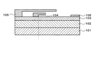
- FIG. 1A shows a conventional AlGaN / GaN HFET using field plate technology.
- a GaN layer 102 and an AlGaN layer 103 are sequentially stacked on a base substrate 101, and a gate electrode 104, a source electrode 105, and a drain electrode 106 are formed on the AlGaN layer 103.
- a gate electrode 104, a source electrode 105, and a drain electrode 106 are formed on the AlGaN layer 103.
- the upper part of the gate electrode 104 and the upper part of the source electrode 105 extend like a hat collar to the drain electrode 106 side to form a field plate.
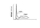
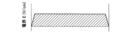
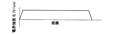
- FIG. 1B shows the electric field distribution with and without the field plate corresponding to FIG. 1A. Since the area of the electric field distribution is equal to the drain voltage, it is possible to improve the breakdown voltage and suppress the current collapse of the AlGaN / GaN HFET by dispersing the peak electric field.
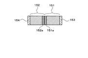
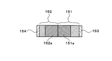
- FIG. 2A shows a conventional pn junction with a small reverse bias voltage applied.
- FIG. 3A shows a superjunction unit unit with a small reverse bias voltage applied.
- a p-type layer 151 and an n-type layer 152 are joined, a p-type layer 151 has a p-electrode 153, and an n-type layer 152 has an n-electrode 154.
- the junction surface of the pn junction is parallel to the p electrode 153 and the n electrode 154.
- a void layer 151a is formed in the vicinity of the bonding surface of the p-type layer 151, and the other part is a p-type neutral region.
- a void layer 152a is formed in the vicinity of the bonding surface of the n-type layer 152, and the other part is an n-type neutral region.
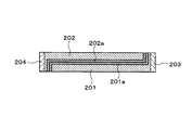
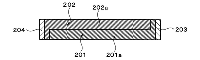
- the p-type layer 201 and the n-type layer 202 form a pn junction as in the conventional pn junction.
- the p-electrode 203 formed on the n-type layer 202 and the n-electrode 204 formed on the n-type layer 202 are formed orthogonal to the main joint surface of the p-type layer 201 and the n-type layer 202 spreading in a planar shape. .
- the joint surfaces are bent in directions opposite to each other with respect to the main joint surface.
- a void layer 201a is formed in the vicinity of the bonding surface of the p-type layer 201, and the other part is a p-type neutral region.
- a void layer 202a is formed in a portion in the vicinity of the bonding surface of the n-type layer 202, and the other portion is an n-type neutral region.
- FIG. 2B shows the electric field distribution of a conventional pn junction in a state where a small reverse bias voltage is applied between the p electrode 153 and the n electrode 154, corresponding to FIG. 2A.
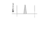
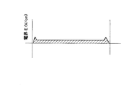
- FIG. 3B shows the electric field distribution of the super junction in a state where a small reverse bias voltage is applied between the p electrode 203 and the n electrode 204, corresponding to FIG. 3A.
- FIG. 4A shows a state where a large reverse bias voltage is applied in a conventional pn junction.
- FIG. 5A shows a state where a large reverse bias voltage is applied in the super junction.
- FIG. 4B shows the electric field distribution of the conventional pn junction in a state where a large reverse bias voltage is applied between the p electrode 153 and the n electrode 154, corresponding to FIG. 4A.
- FIG. 5B shows the electric field distribution of the super junction in a state where a large reverse bias voltage is applied between the p electrode 203 and the n electrode 204, corresponding to FIG. 5A.
- the spread of the depletion layers 151a, 152a, 201a, and 202a occurs from the pn junction surface as in the conventional pn junction and super junction.
- the electric field distribution due to fixed charges such as acceptor ions and donor ions in the depletion layers 151a and 152a is triangular as shown in FIGS. 2B and 4B, and a peak electric field distribution is generated.
- the super junction as shown in FIGS. 3B and 5B, even if the depletion layers 201a and 202a spread, the electric field (integrated value of charges) is constant in the direction connecting the p electrode 203 and the n electrode 204. It can be seen that the electric field concentration does not occur.
- the applied voltage is an integral value of the electric field (in FIG. 2B, FIG. 3B, FIG. 4B, and FIG. 5B, it corresponds to the area of the electric field)
- the withstand voltage of the conventional pn junction is limited by the maximum electric field strength generated on the joint surface.
- the superjunction can handle and withstand the applied voltage with a uniform electric field over the entire semiconductor.
- the superjunction is applied to the drift layer of Si-MOS power transistors and Si power diodes having vertical and horizontal structures.
- Patent Document 1 there is a principle of polarization junction as a method of generating positive charge and negative charge distribution similar to that of a super junction without depending on a pn junction (see, for example, Patent Document 1).
- Patent Document 2 a technique aiming at a high breakdown voltage using polarization has been proposed (see, for example, Patent Document 2).
- This semiconductor element includes an In z Ga 1-z N layer (0 ⁇ z ⁇ 1), an Al x Ga 1-x N layer (0 ⁇ x ⁇ 1), an In y Ga 1-y N layer (0 ⁇ y ⁇ 1) and a p-type In w Ga 1-w N layer (0 ⁇ w ⁇ 1) are sequentially stacked, and when not operating, an Al x Ga 1-x N layer and an In y Ga 1-y N layer Two-dimensional hole gas is formed in the In y Ga 1-y N layer in the vicinity of the hetero interface between the layers, and the In z Ga 1-z N layer, the Al x Ga 1-x N layer, A two-dimensional electron gas is formed in the In z Ga 1 -z N layer in the vicinity of the hetero interface between the two layers.
- the surface GaN layer is doped with Mg, the band near the surface is lifted by the negative fixed charge of the Mg acceptor, and a sufficient amount of 2 is added to the AlGaN / GaN heterointerface on the surface side. It is improved to generate a dimensional hole gas.
- the first transistor that substantially utilizes the polarization effect was announced (see Non-Patent Document 4).
- Patent Document 3 Since the semiconductor element using the polarization super-junction (PJ) proposed in Patent Document 3 and Non-Patent Document 3 uses the same principle as the Si super-junction method, the field plate conventionally proposed In principle, a super withstand voltage element can be obtained more easily than the method. However, according to a study conducted independently by the present inventors, it has become clear that the operation (dynamics, dynamic characteristics) is limited by the speed of hole movement.
- PJ polarization super-junction
- the surface p-type GaN layer in the semiconductor elements of Patent Document 3 and Non-Patent Document 3 is introduced in order to cancel out the surface level, and the total amount of acceptors has an appropriate value. If the total amount of acceptors is too large, in addition to the channel two-dimensional electron gas, a large amount of holes derived from the acceptors are generated, the charge balance with the channel electrons is lost, and the breakdown voltage is reduced. However, a p-side ohmic electrode (p-electrode) is formed on a part of the surface of the p-type GaN layer to extract or introduce holes as the device operates. Ohmic contact cannot be obtained.
- An object of the present invention is to provide a low-loss semiconductor element and a bidirectional field-effect transistor that can be overcome, have a high breakdown voltage, eliminate the occurrence of current collapse, and can operate at high speed.
- Another problem to be solved by the present invention is to provide a high-performance electric device using the semiconductor element or the bidirectional field effect transistor.
- Still another problem to be solved by the present invention is to provide a mounting structure including the semiconductor element or the bidirectional field effect transistor.
- the present invention provides: A polarization superjunction region and a p-electrode contact region provided separately from each other;
- the polarization superjunction region is A first undoped GaN layer;
- the thickness of the second undoped GaN layer is represented by u [nm]
- the thickness of the p-type GaN layer is represented by v [nm]
- the Mg concentration of the p-type GaN layer is represented by w [cm ⁇ 3 ].
- the p-electrode contact region is A p-type GaN contact layer doped with Mg at a higher concentration than the p-type GaN layer provided in contact with the p-type GaN layer only in the p-electrode contact region; A p-electrode in ohmic contact with the p-type GaN contact layer;
- a two-dimensional hole gas is formed in the second undoped GaN layer in the vicinity of the heterointerface between the undoped Al x Ga 1-x N layer and the second undoped GaN layer.
- the p-type GaN contact layer is not particularly limited as long as it is in contact with the p-type GaN layer.
- the p-type GaN contact layer may be formed in a mesa shape on the p-type GaN layer, or may be embedded in a p-type GaN layer or the like.
- a groove is provided at a depth reaching at least the undoped Al x Ga 1-x N layer in the undoped Al x Ga 1-x N layer, the second undoped GaN layer, and the p-type GaN layer.
- a p-type GaN contact layer is buried inside, and the p-type GaN contact layer and the two-dimensional hole gas are joined.
- a p-type GaN layer is grown sequentially.
- the first undoped GaN layer and the undoped Al x Ga 1-x N layer and / or the second undoped GaN layer and the undoped Al x Ga 1-x N layer are used as necessary.
- an undoped Al u Ga 1-u N layer (0 ⁇ u ⁇ 1, u> x), for example an AlN layer, is provided.
- Al u Ga 1-u N layer between the first undoped GaN layer and the undoped Al x Ga 1-x N layer, an undoped a first undoped GaN layer Al x Ga 1-x N
- This Al u Ga 1-u N layer or AlN layer may generally be sufficiently thin, for example, about 1 to 2 nm is sufficient.
- the semiconductor element can be used as various elements, but typically can be used as a field effect transistor (FET), a diode, or the like.
- FET field effect transistor
- the field effect transistor can be configured as follows, for example.
- the second undoped GaN layer and the p-type GaN layer on the undoped Al x Ga 1-x N layer are patterned into a mesa shape, and the p-type GaN contact layer is a mesa shape on the p-type GaN layer.
- a source electrode and a drain electrode are provided on the undoped Al x Ga 1-x N layer with the second undoped GaN layer and the p-type GaN layer interposed therebetween, and the source electrode, the second undoped GaN layer, and the p-type GaN are provided.
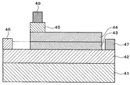
- a gate electrode is provided on the undoped Al x Ga 1-x N layer between the layers, and a p electrode is provided on the p-type GaN contact layer.
- the second undoped GaN layer and the p-type GaN layer on the undoped Al x Ga 1-x N layer are patterned into a mesa shape, and the p-type GaN contact layer is a mesa shape on the p-type GaN layer.
- a source electrode and a drain electrode are provided on the undoped Al x Ga 1-x N layer with the second undoped GaN layer and the p-type GaN layer interposed therebetween, and the source electrode, the second undoped GaN layer, and the p-type GaN are provided.
- a gate electrode also serving as a p-electrode extends on the p-type GaN contact layer from the end faces of the second undoped GaN layer and the p-type GaN layer on the undoped Al x Ga 1-x N layer between the layers Provided.
- the second undoped GaN layer and the p-type GaN layer on the undoped Al x Ga 1-x N layer are patterned into a mesa shape, and the p-type GaN contact layer is a mesa shape on the p-type GaN layer.
- a source electrode and a drain electrode are provided on the undoped Al x Ga 1-x N layer with the second undoped GaN layer and the p-type GaN layer interposed therebetween, and the source electrode, the second undoped GaN layer, and the p-type GaN are provided.
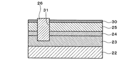
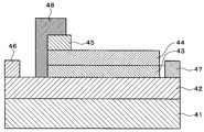
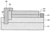
- Grooves are provided in the undoped Al x Ga 1-x N layer between the layers and connected to the end faces of the second undoped GaN layer and the p-type GaN layer, and a gate electrode that also serves as a p-electrode is provided inside the groove. And extends from the end faces of the second undoped GaN layer and the p-type GaN layer onto the p-type GaN contact layer.
- the second undoped GaN layer and the p-type GaN layer on the undoped Al x Ga 1-x N layer are patterned into a mesa type, and the p-type GaN contact layer is a mesa type on the p-type GaN layer.
- a source electrode and a drain electrode are provided on the undoped Al x Ga 1-x N layer with the second undoped GaN layer and the p-type GaN layer sandwiched therebetween, and p serving as a gate electrode on the p-type GaN contact layer An electrode is provided.
- a groove is provided in the undoped Al x Ga 1-x N layer, the second undoped GaN layer, and the p-type GaN layer at a depth reaching at least the undoped Al x Ga 1-x N layer.
- a p-type GaN contact layer is buried inside the p-type GaN contact layer and the two-dimensional hole gas is bonded to the p-type GaN contact layer, the second undoped GaN layer on the undoped Al x Ga 1-x N layer and p
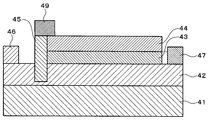
- the p-type GaN layer is patterned into a mesa shape, and a source electrode and a drain electrode are provided on the undoped Al x Ga 1-x N layer with the second undoped GaN layer and the p-type GaN layer sandwiched therebetween, and on the p-type GaN contact layer Is provided with a p-electrode also serving as a gate electrode.
- the diode can be configured as follows, for example.
- the second undoped GaN layer and the p-type GaN layer on the undoped Al x Ga 1-x N layer are patterned into a mesa shape, and the p-type GaN contact layer is a mesa shape on the p-type GaN layer.
- An anode electrode and a cathode electrode are provided across the second undoped GaN layer and the p-type GaN layer, and the anode electrode is embedded in at least a groove provided in the undoped Al x Ga 1-x N layer.
- the second undoped GaN layer and the p-type GaN layer on the undoped Al x Ga 1-x N layer are patterned into a mesa shape, and the p-type GaN contact layer is a mesa shape on the p-type GaN layer.
- An anode electrode and a cathode electrode are provided on the undoped Al x Ga 1-x N layer with the second undoped GaN layer and the p-type GaN layer interposed therebetween.
- the anode electrode, the second undoped GaN layer, and the p-type GaN Grooves are provided in the undoped Al x Ga 1-x N layer between the layers and connected to the end faces of the second undoped GaN layer and the p-type GaN layer, and a p-electrode is embedded in the groove, The end surfaces of the second undoped GaN layer and the p-type GaN layer extend on the p-type GaN contact layer and are electrically connected to the anode electrode.
- a groove is provided in the undoped Al x Ga 1-x N layer, the second undoped GaN layer, and the p-type GaN layer at a depth reaching at least the undoped Al x Ga 1-x N layer.
- the second undoped GaN layer on the undoped Al x Ga 1-x N layer and p The type GaN layer is patterned into a mesa shape, and an anode electrode and a cathode electrode are provided across the second undoped GaN layer and the p-type GaN layer, and reach at least the first undoped GaN layer connected to the p-type GaN contact layer.
- Another groove of depth is provided, the gate electrode is embedded inside this another groove, further extends on the p-type GaN contact layer, and the cathode electrode is AND Provided flops Al x Ga 1-x N layer.
- the polarization superjunction region is A first undoped GaN layer; An undoped or doped Al x Ga 1-x N layer (0 ⁇ x ⁇ 1) on the first undoped GaN layer; A second undoped GaN layer on the undoped or doped Al x Ga 1-x N layer; A p-type GaN layer doped with Mg on the second undoped GaN layer; The undoped or doped Al x Ga 1-x N layer comprises the first undoped GaN layer and the undoped or doped Al x Ga 1-x N layer on the first undoped GaN layer.
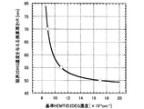
- a reference HEMT having a structure having an Al composition x and thickness such that the two-dimensional electron gas concentration of the reference HEMT is 0.89 ⁇ 10 13 cm ⁇ 2 or more and 1.70 ⁇ 10 13 cm ⁇ 2 or less;
- the thickness of the undoped GaN layer is represented by u [nm]
- the thickness of the p-type GaN layer is represented by v [nm]
- the Mg concentration of the p-type GaN layer is represented by w [cm ⁇ 3 ].
- the p-electrode contact region is A p-type GaN contact layer doped with Mg at a higher concentration than the p-type GaN layer provided in contact with the p-type GaN layer only in the p-electrode contact region; A p-electrode in ohmic contact with the p-type GaN contact layer; When not in operation, a two-dimensional hole is formed in the second undoped GaN layer in the vicinity of the heterointerface between the undoped or doped Al x Ga 1-x N layer and the second undoped GaN layer.
- a gas is formed and the first undoped GaN layer is two-dimensionally in a portion in the vicinity of the heterointerface between the first undoped GaN layer and the undoped or doped Al x Ga 1-x N layer.
- Patent Document 3 is valid as long as it is not contrary to the nature of the invention.
- this invention Having at least one semiconductor element;
- the semiconductor element is A polarization superjunction region and a p-electrode contact region provided separately from each other;
- the polarization superjunction region is A first undoped GaN layer;
- An undoped Al x Ga 1-x N layer (0.17 ⁇ x ⁇ 0.35) having a thickness of 25 nm to 47 nm on the first undoped GaN layer;
- the thickness of the second undoped GaN layer is represented by u [nm]
- the thickness of the p-type GaN layer is represented by v [nm]
- the Mg concentration of the p-type GaN layer is represented by w [cm ⁇ 3 ].
- the p-electrode contact region is A p-type GaN contact layer doped with Mg at a higher concentration than the p-type GaN layer provided in contact with the p-type GaN layer only in the p-electrode contact region; A p-electrode in ohmic contact with the p-type GaN contact layer;
- a two-dimensional hole gas is formed in the second undoped GaN layer in the vicinity of the heterointerface between the undoped Al x Ga 1-x N layer and the second undoped GaN layer.
- a semiconductor element in which a two-dimensional electron gas is formed in the first undoped GaN layer in the vicinity of the heterointerface between the first undoped GaN layer and the undoped Al x Ga 1-x N layer It is an
- this invention Having at least one semiconductor element;
- the semiconductor element is A polarization superjunction region and a p-electrode contact region provided separately from each other;
- the polarization superjunction region is A first undoped GaN layer;
- the undoped or doped Al x Ga 1-x N layer comprises the first undoped GaN layer and the undoped or doped Al x Ga 1-x N layer on the first undoped GaN layer.
- a reference HEMT having a structure having an Al composition x and thickness such that the two-dimensional electron gas concentration of the reference HEMT is 0.89 ⁇ 10 13 cm ⁇ 2 or more and 1.70 ⁇ 10 13 cm ⁇ 2 or less;
- the thickness of the undoped GaN layer is represented by u [nm]
- the thickness of the p-type GaN layer is represented by v [nm]
- the Mg concentration of the p-type GaN layer is represented by w [cm ⁇ 3 ].
- the p-electrode contact region is A p-type GaN contact layer doped with Mg at a higher concentration than the p-type GaN layer provided in contact with the p-type GaN layer only in the p-electrode contact region; A p-electrode in ohmic contact with the p-type GaN contact layer; When not in operation, a two-dimensional hole is formed in the second undoped GaN layer in the vicinity of the heterointerface between the undoped or doped Al x Ga 1-x N layer and the second undoped GaN layer.
- a gas is formed and the first undoped GaN layer is two-dimensionally in a portion in the vicinity of the heterointerface between the first undoped GaN layer and the undoped or doped Al x Ga 1-x N layer. It is an electrical device that is a semiconductor element in which an electron gas is formed.
- the electric equipment includes almost all of the equipment that uses electricity, regardless of the application, function, size, etc., but is, for example, an electronic equipment, a moving body, a power unit, a construction machine, a machine tool, or the like.
- Electronic devices include robots, computers, game devices, in-vehicle devices, home appliances (air conditioners, etc.), industrial products, mobile phones, mobile devices, IT devices (servers, etc.), power conditioners used in solar power generation systems, power transmission Such as a system.
- the moving body is a railway vehicle, an automobile (such as an electric vehicle), a two-wheeled vehicle, an aircraft, a rocket, or a spacecraft.
- the polarization superjunction region is A first undoped GaN layer; An undoped Al x Ga 1-x N layer (0.17 ⁇ x ⁇ 0.35) having a thickness of 25 nm to 47 nm on the first undoped GaN layer; A second undoped GaN layer on the undoped Al x Ga 1-x N layer; A p-type GaN layer doped with Mg on the second undoped GaN layer; The thickness of the second undoped GaN layer is represented by u [nm], the thickness of the p-type GaN layer is represented by v [nm], and the Mg concentration of the p-type GaN layer is represented by w [cm ⁇ 3 ].
- the second undoped GaN layer and the p-type GaN layer have a mesa shape
- a first source electrode and a second source electrode are provided on the undoped Al x Ga 1-x N layer across the second undoped GaN layer and the p-type GaN layer
- the p-electrode contact region is A first p-type GaN contact layer doped with Mg at a higher concentration than the p-type GaN layer provided in contact with the p-type GaN layer only in the p-electrode contact region;
- Two p-type GaN contact layers A first p electrode constituting a first gate electrode in ohmic contact with the first p-type GaN contact layer; A second p electrode constituting a second gate electrode in ohmic contact with the second p-type GaN contact layer;
- a two-dimensional hole gas is formed in the second undoped GaN layer in the vicinity of the heterointerface between the undoped Al x Ga 1-x N layer and the second undoped GaN layer.
- two-dimensional electron gas is formed in the first undoped GaN layer in the vicinity of the heterointerface between the first undoped GaN layer and the undoped Al x Ga 1-x N layer. It is a field effect transistor.
- the polarization superjunction region is A first undoped GaN layer; An undoped or doped Al x Ga 1-x N layer (0 ⁇ x ⁇ 1) on the first undoped GaN layer; A second undoped GaN layer on the undoped or doped Al x Ga 1-x N layer; A p-type GaN layer doped with Mg on the second undoped GaN layer; The undoped or doped Al x Ga 1-x N layer comprises the first undoped GaN layer and the undoped or doped Al x Ga 1-x N layer on the first undoped GaN layer.
- a reference HEMT having a structure having an Al composition x and thickness such that the two-dimensional electron gas concentration of the reference HEMT is 0.89 ⁇ 10 13 cm ⁇ 2 or more and 1.70 ⁇ 10 13 cm ⁇ 2 or less;
- the thickness of the undoped GaN layer is represented by u [nm]
- the thickness of the p-type GaN layer is represented by v [nm]
- the Mg concentration of the p-type GaN layer is represented by w [cm ⁇ 3 ].
- the second undoped GaN layer and the p-type GaN layer have a mesa shape, A first source electrode and a second source electrode are provided on the undoped or doped Al x Ga 1-x N layer across the second undoped GaN layer and the p-type GaN layer;
- the p-electrode contact region is A first p-type GaN contact layer doped with Mg at a higher concentration than the p-type GaN layer provided in contact with the p-type GaN layer only in the p-electrode contact region; A first layer doped with Mg at a higher concentration than the p-type GaN layer provided in contact with the p-type
- Two p-type GaN contact layers A first p electrode constituting a first gate electrode in ohmic contact with the first p-type GaN contact layer; A second p electrode constituting a second gate electrode in ohmic contact with the second p-type GaN contact layer;
- a two-dimensional hole is formed in the second undoped GaN layer in the vicinity of the heterointerface between the undoped or doped Al x Ga 1-x N layer and the second undoped GaN layer.
- a gas is formed and the first undoped GaN layer is two-dimensionally in a portion in the vicinity of the heterointerface between the first undoped GaN layer and the undoped or doped Al x Ga 1-x N layer.
- a bidirectional field effect transistor in which an electron gas is formed.
- this invention Has one or more bidirectional switches, At least one of the bidirectional switches is A polarization superjunction region and a p-electrode contact region provided separately from each other;
- the polarization superjunction region is A first undoped GaN layer;
- the thickness of the second undoped GaN layer is represented by u [nm]
- the thickness of the p-type GaN layer is represented by v [nm]
- the Mg concentration of the p-type GaN layer is represented by w [cm ⁇ 3 ].
- Two p-type GaN contact layers A first p electrode constituting a first gate electrode in ohmic contact with the first p-type GaN contact layer; A second p electrode constituting a second gate electrode in ohmic contact with the second p-type GaN contact layer;
- a two-dimensional hole gas is formed in the second undoped GaN layer in the vicinity of the heterointerface between the undoped Al x Ga 1-x N layer and the second undoped GaN layer.
- two-dimensional electron gas is formed in the first undoped GaN layer in the vicinity of the heterointerface between the first undoped GaN layer and the undoped Al x Ga 1-x N layer. It is an electric device which is a field effect transistor.
- this invention Has one or more bidirectional switches, At least one of the bidirectional switches is A polarization superjunction region and a p-electrode contact region provided separately from each other;
- the polarization superjunction region is A first undoped GaN layer;
- the undoped or doped Al x Ga 1-x N layer comprises the first undoped GaN layer and the undoped or doped Al x Ga 1-x N layer on the first undoped GaN layer.
- the second undoped GaN layer and the p-type GaN layer have a mesa shape, A first source electrode and a second source electrode are provided on the undoped or doped Al x Ga 1-x N layer across the second undoped GaN layer and the p-type GaN layer;
- the p-electrode contact region is A first p-type GaN contact layer doped with Mg at a higher concentration than the p-type GaN layer provided in contact with the p-type GaN layer only in the p-electrode contact region; A first layer doped with Mg at a higher concentration than the p-type GaN layer provided in contact with the p-type
- Two p-type GaN contact layers A first p electrode constituting a first gate electrode in ohmic contact with the first p-type GaN contact layer; A second p electrode constituting a second gate electrode in ohmic contact with the second p-type GaN contact layer;
- a two-dimensional hole is formed in the second undoped GaN layer in the vicinity of the heterointerface between the undoped or doped Al x Ga 1-x N layer and the second undoped GaN layer.
- a gas is formed and the first undoped GaN layer is two-dimensionally in a portion in the vicinity of the heterointerface between the first undoped GaN layer and the undoped or doped Al x Ga 1-x N layer.
- An electrical device that is a bidirectional field effect transistor in which an electron gas is formed.
- ⁇ Electric devices using the bidirectional field effect transistor include matrix converters and multi-level inverters in addition to those already mentioned.
- this invention A chip constituting a semiconductor element; A mounting substrate on which the chip is flip-chip mounted;
- the semiconductor element is A polarization superjunction region and a p-electrode contact region provided separately from each other;
- the polarization superjunction region is A first undoped GaN layer;
- An undoped Al x Ga 1-x N layer (0.17 ⁇ x ⁇ 0.35) having a thickness of 25 nm to 47 nm on the first undoped GaN layer;
- the thickness of the second undoped GaN layer is represented by u [nm]
- the thickness of the p-type GaN layer is represented by v [nm]
- the Mg concentration of the p-type GaN layer is represented by w [cm ⁇ 3 ].
- the p-electrode contact region is A p-type GaN contact layer doped with Mg at a higher concentration than the p-type GaN layer provided in contact with the p-type GaN layer only in the p-electrode contact region; A p-electrode in ohmic contact with the p-type GaN contact layer;
- a two-dimensional hole gas is formed in the second undoped GaN layer in the vicinity of the heterointerface between the undoped Al x Ga 1-x N layer and the second undoped GaN layer.
- a semiconductor element in which a two-dimensional electron gas is formed in the first undoped GaN layer in the vicinity of the heterointerface between the first undoped GaN layer and the undoped Al x Ga 1-x N layer Is
- this invention A chip constituting a semiconductor element; A mounting substrate on which the chip is flip-chip mounted;
- the semiconductor element is A polarization superjunction region and a p-electrode contact region provided separately from each other;
- the polarization superjunction region is A first undoped GaN layer;
- the undoped or doped Al x Ga 1-x N layer comprises the first undoped GaN layer and the undoped or doped Al x Ga 1-x N layer on the first undoped GaN layer.
- a reference HEMT having a structure having an Al composition x and thickness such that the two-dimensional electron gas concentration of the reference HEMT is 0.89 ⁇ 10 13 cm ⁇ 2 or more and 1.70 ⁇ 10 13 cm ⁇ 2 or less;
- the thickness of the undoped GaN layer is represented by u [nm]
- the thickness of the p-type GaN layer is represented by v [nm]
- the Mg concentration of the p-type GaN layer is represented by w [cm ⁇ 3 ].
- the p-electrode contact region is A p-type GaN contact layer doped with Mg at a higher concentration than the p-type GaN layer provided in contact with the p-type GaN layer only in the p-electrode contact region; A p-electrode in ohmic contact with the p-type GaN contact layer; When not in operation, a two-dimensional hole is formed in the second undoped GaN layer in the vicinity of the heterointerface between the undoped or doped Al x Ga 1-x N layer and the second undoped GaN layer.
- a gas is formed and the first undoped GaN layer is two-dimensionally in a portion in the vicinity of the heterointerface between the first undoped GaN layer and the undoped or doped Al x Ga 1-x N layer. It is a mounting structure which is a semiconductor element in which an electron gas is formed.
- this invention A chip constituting a semiconductor element; A mounting substrate on which the chip is flip-chip mounted;
- the semiconductor element is A polarization superjunction region and a p-electrode contact region provided separately from each other;
- the polarization superjunction region is A first undoped GaN layer;
- An undoped Al x Ga 1-x N layer (0.17 ⁇ x ⁇ 0.35) having a thickness of 25 nm to 47 nm on the first undoped GaN layer;
- the thickness of the second undoped GaN layer is represented by u [nm]
- the thickness of the p-type GaN layer is represented by v [nm]
- the Mg concentration of the p-type GaN layer is represented by w [cm ⁇ 3 ].
- the second undoped GaN layer and the p-type GaN layer have a mesa shape
- a first source electrode and a second source electrode are provided on the undoped Al x Ga 1-x N layer across the second undoped GaN layer and the p-type GaN layer
- the p-electrode contact region is A first p-type GaN contact layer doped with Mg at a higher concentration than the p-type GaN layer provided in contact with the p-type GaN layer only in the p-electrode contact region;
- Two p-type GaN contact layers A first p electrode constituting a first gate electrode in ohmic contact with the first p-type GaN contact layer; A second p electrode constituting a second gate electrode in ohmic contact with the second p-type GaN contact layer;
- a two-dimensional hole gas is formed in the second undoped GaN layer in the vicinity of the heterointerface between the undoped Al x Ga 1-x N layer and the second undoped GaN layer.
- two-dimensional electron gas is formed in the first undoped GaN layer in the vicinity of the heterointerface between the first undoped GaN layer and the undoped Al x Ga 1-x N layer. It is a mounting structure which is a field effect transistor.
- this invention A chip constituting a semiconductor element; A mounting substrate on which the chip is flip-chip mounted;
- the semiconductor element is A polarization superjunction region and a p-electrode contact region provided separately from each other;
- the polarization superjunction region is A first undoped GaN layer;
- the undoped or doped Al x Ga 1-x N layer comprises the first undoped GaN layer and the undoped or doped Al x Ga 1-x N layer on the first undoped GaN layer.
- a reference HEMT having a structure having an Al composition x and thickness such that the two-dimensional electron gas concentration of the reference HEMT is 0.89 ⁇ 10 13 cm ⁇ 2 or more and 1.70 ⁇ 10 13 cm ⁇ 2 or less;
- the thickness of the undoped GaN layer is represented by u [nm]
- the thickness of the p-type GaN layer is represented by v [nm]
- the Mg concentration of the p-type GaN layer is represented by w [cm ⁇ 3 ].
- the second undoped GaN layer and the p-type GaN layer have a mesa shape, A first source electrode and a second source electrode are provided on the undoped Al x Ga 1-x N layer across the second undoped GaN layer and the p-type GaN layer;
- the p-electrode contact region is A first p-type GaN contact layer doped with Mg at a higher concentration than the p-type GaN layer provided in contact with the p-type GaN layer only in the p-electrode contact region; A first layer doped with Mg at a higher concentration than the p-type GaN layer provided in contact with the p-type GaN layer
- the bidirectional field effect transistor, and the mounting structure In the invention of the electric device, the bidirectional field effect transistor, and the mounting structure, what has been described in relation to the invention of the two semiconductor elements is valid as long as it is not contrary to the nature thereof.
- the mounting substrate in the mounting structure a substrate having good thermal conductivity is used, and it is appropriately selected from conventionally known substrates.
- the two-dimensional generated in the second undoped GaN layer in the vicinity of the heterointerface between the undoped Al x Ga 1-x N layer and the second undoped GaN layer during non-operation can be 1 ⁇ 10 12 cm ⁇ 2 or more.
- the peak electric field generated in the local part of the conduction channel is fundamentally reduced, the generation of current collapse can be eliminated at the same time as the withstand voltage is increased, and the low-loss semiconductor element capable of high-speed operation and the bidirectional electric field An effect transistor can be easily realized.
- a high-performance electric device can be realized by using the semiconductor element or the bidirectional field effect transistor.
- a mounting structure in which a chip that constitutes a semiconductor element or a bidirectional field effect transistor is flip-chip mounted on a mounting substrate excellent heat dissipation is achieved even when the semiconductor element or the bidirectional field effect transistor is formed on an insulating substrate. Obtainable.
- FIG. 4A It is a basic diagram which shows the electric field distribution in the pn junction shown to FIG. 4A. It is sectional drawing which shows the super junction in the state where the big reverse bias voltage was applied. It is a basic diagram which shows the electric field distribution in the super junction shown to FIG. 5A.
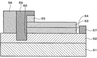
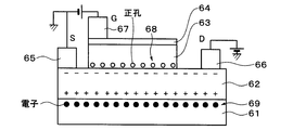
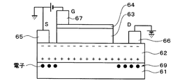
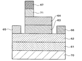
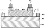
- 1 is a cross-sectional view showing a basic structure of a GaN-based semiconductor device according to a first embodiment of the present invention. It is a basic diagram which shows the energy band structure of the GaN-type semiconductor element by 1st Embodiment of this invention. It is a basic diagram for demonstrating operation
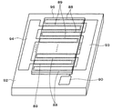
- FIG. 5 is a schematic diagram showing a relationship between a distance between electrodes measured using a TLM measurement sample manufactured using samples 1 to 4 and resistance.
- FIG. 14A It is a top view which shows the hall
- FIG. 6 is a cross-sectional view showing samples 8 to 12 produced in Experiment 4 conducted for consideration of the GaN-based semiconductor device according to the first embodiment of the present invention.
- FIG. 11 is a cross-sectional view showing a hole measurement sample manufactured using Samples 8 to 13. It is sectional drawing which shows the sample 20 used in Experiment 5 performed in order to consider the GaN-type semiconductor element by 1st Embodiment of this invention.
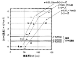
- FIG. 6 is a schematic diagram showing a relationship between a converted thickness tR of samples 8 to 23 and a measured 2DHG concentration. It is a basic diagram which expands and shows a part of FIG. P. 272 FIG.
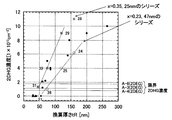
- FIG. 1 is a schematic diagram in which data of comparative samples A-3, A-4, and A-6 are written in FIG.
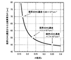
- FIG. 6 is a schematic diagram showing a relationship between a converted thickness tR of samples 24 to 31 and a measured 2DHG concentration. It is a basic diagram which expands and shows a part of FIG. It is a schematic diagram showing the relationship between the conversion thickness tR give undoped Al x Ga 1-x N Al composition x and limitations 2DHG concentration layer. It is sectional drawing for demonstrating the method for producing a polarization superjunction region and a p-electrode contact region in the GaN-based semiconductor device according to the first embodiment of the present invention.
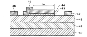
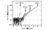
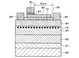
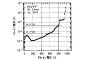
- FIG. 48 is a schematic diagram showing a measurement result of drain current-drain voltage characteristics of the GaN-based field effect transistor shown in FIG. 47. It is sectional drawing which shows the GaN-type field effect transistor on the sapphire substrate for demonstrating the mounting structure by 5th Embodiment of this invention.
- FIG. 48 is a schematic diagram showing a measurement result of drain current-drain voltage characteristics of the GaN-based field effect transistor shown in FIG. 47. It is sectional drawing which shows the GaN-type field effect transistor on the sapphire substrate for demonstrating the mounting structure by 5th Embodiment of this invention.
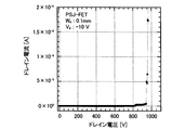
- FIG. 50 is a schematic diagram showing a measurement result of drain current-drain voltage characteristics of the GaN-based field effect transistor shown in FIG. 49.
- FIG. 50 is a schematic diagram showing a measurement result of drain current-drain voltage characteristics of the GaN-based field effect transistor shown in FIG. 49.
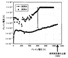
- It is a basic diagram which shows the measurement result of the drain current-drain voltage characteristic of the GaN-type field effect transistor on Si substrate for demonstrating the mounting structure by 5th Embodiment of this invention.
- the current collapse measurement result of the GaN-based field effect transistor on the sapphire substrate and the current collapse measurement result of the GaN-based HFET on the conventional sapphire substrate for explaining the mounting structure according to the fifth embodiment of the present invention are shown.
- FIG. 50 is a schematic diagram showing a measurement result of drain current-drain voltage characteristics of the GaN-based field effect transistor shown in FIG. 49.
- FIG. 50 is a schematic diagram showing a measurement result of drain current-drain voltage characteristics of the GaN-based field
- FIG. 1 A GaN-based semiconductor device according to the first embodiment will be described.
- This GaN-based semiconductor element is a polarization superjunction element.
- the basic structure of this GaN-based semiconductor element is shown in FIG.
- this GaN-based semiconductor element has a polarization superjunction region and a p-electrode contact region region provided separately from each other.
- a polarization superjunction region In the polarization superjunction region, an undoped GaN layer 11 and an undoped Al x Ga layer having a thickness of 25 nm to 47 nm on a base substrate (not shown) such as a C-plane sapphire substrate on which a GaN-based semiconductor grows in the C plane.
- a 1-x N layer 12 (0.17 ⁇ x ⁇ 0.35), an undoped GaN layer 13 and a p-type GaN layer 14 doped with Mg are sequentially stacked.
- a p-type GaN contact layer (hereinafter referred to as “p”) which is in contact with the p-type GaN layer 14 only in this p-electrode contact region and is doped with Mg at a higher concentration than the p-type GaN layer 14.
- p p-type GaN contact layer
- a p-electrode is electrically connected to the p-type GaN contact layer.
- FIG. 6 as an example, a case where a mesa-type p + -type GaN contact layer 15 is stacked on the p-type GaN layer 14 is shown.
- this GaN-based semiconductor element in a non-operating state, in a portion near the heterointerface between the undoped GaN layer 11 and the undoped Al x Ga 1-x N layer 12 near the base substrate due to piezoelectric polarization and spontaneous polarization.
- positive fixed charge in the undoped Al x Ga 1-x N layer 12 is induced, and the vicinity of the hetero interface between the undoped Al x Ga 1-x N layer 12 and the undoped GaN layer 13 of the base substrate opposite A negative fixed charge is induced in the undoped Al x Ga 1-x N layer 12 in this portion.
- FIG. 7 shows the energy band structure of this GaN-based semiconductor element.
- E v is the energy at the upper end of the valence band
- E c is the energy at the lower end of the conduction band
- E F is the Fermi level.
- the undoped GaN layer 13 alone compensates for the negative fixed charge due to polarization by the surface level.
- the 2DHG 16 is not formed in the undoped GaN layer 13 in the vicinity of the heterointerface between the Al x Ga 1-x N layer 12 and the undoped GaN layer 13. Therefore, by providing the p-type GaN layer 14 on the undoped GaN layer 13, and pull up the energy E v at the upper end of the valence band of the p-type GaN layer 14 to the Fermi level E F.
- the 2DHG 16 is formed in the undoped GaN layer 13 in the vicinity of the heterointerface between the undoped Al x Ga 1-x N layer 12 and the undoped GaN layer 13.
- 2DEG 17 is formed in the undoped GaN layer 11 in the vicinity of the heterointerface between the undoped GaN layer 11 and the undoped Al x Ga 1-x N layer 12.
- an anode electrode 18 is formed on one end face of the p-type GaN layer 14 so as to extend to the position of 2DHG 16, and one of the undoped Al x Ga 1-x N layer 12 is formed.
- the cathode electrode 19 is formed so as to extend to the position of 2DEG 17 on the end face.
- the anode electrode 18 is made of, for example, Ni
- the cathode electrode 19 is made of, for example, a Ti / Al / Au multilayer film.
- a reverse bias voltage is applied between the anode electrode 18 and the cathode electrode 19.
- FIG. 8B shows the electric field distribution along the undoped Al x Ga 1-x N layer 12 at this time. As shown in FIG.
- the concentrations of 2DHG16 and 2DEG17 are both reduced by an equal amount, and both ends of 2DHG16 and 2DEG17 are vacant. Even if the concentrations of 2DHG16 and 2DEG17 are changed by an equal amount, the amount of change in charge is substantially zero, so that the electric field distribution becomes a superjunction electric field distribution and no peak is generated in the electric field. Therefore, it is possible to improve the high pressure resistance and the low current collapse performance.
- the thickness of the undoped GaN layer 13 is u [nm]
- the thickness of the p-type GaN layer 14 is v [nm]
- the Mg concentration of the p-type GaN layer 14 is w [cm ⁇ ].
- tR u + v (1 + w ⁇ 10 ⁇ 18 )
- tR 0.864 / (x ⁇ 0.134) +46.0 [nm]
- 2DHG 16 having a concentration of 1 ⁇ 10 12 cm ⁇ 2 or more can be generated.
- a polarization superjunction region and a p-electrode contact region are provided separately from each other, a p + -type GaN contact layer 15 is provided in contact with the p-type GaN layer 14 only in the p-electrode contact region, and tR ⁇ 0.864 /
- the basis for setting (x ⁇ 0.134) +46.0 [nm] will be described below.
- Samples 1 to 4 were prepared in order to investigate the necessary conditions (acceptor concentration and thickness) of the p + -type GaN contact layer.
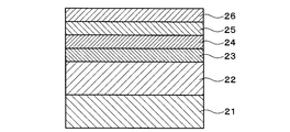
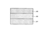
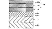
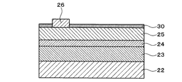
- Sample 1 was prepared as follows. As shown in FIG. 9, TMG (trimethylgallium) as a Ga source and TMA (trimethyl) as an Al source are formed on a (0001) plane, that is, a C-plane sapphire substrate 21 by a conventionally known MOCVD (metal organic chemical vapor deposition) method.
- MOCVD metal organic chemical vapor deposition
- the p + -type GaN contact layer 26 of Mg-doped was grown.
- Sample 2 was fabricated in the same manner as Sample 1, except that the p + -type GaN contact layer 26 had a thickness of 120 nm.
- a low-temperature growth (530 ° C.) GaN buffer layer (not shown) having a thickness of 30 nm is stacked on the C-plane sapphire substrate 21 by MOCVD,
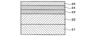
- Sample 4 was a standard sample and was prepared as follows. As shown in FIG. 11, a low-temperature growth (530 ° C.) GaN buffer layer (not shown) having a thickness of 30 nm is stacked on the C-plane sapphire substrate 21 by MOCVD, and then the growth temperature is increased to 1100 ° C. An 800-nm-thick undoped GaN layer 22 and a 600-nm-thick Mg-doped p-type GaN layer 25 having an Mg concentration of 5.0 ⁇ 10 19 cm ⁇ 3 were grown.
- a low-temperature growth (530 ° C.) GaN buffer layer (not shown) having a thickness of 30 nm is stacked on the C-plane sapphire substrate 21 by MOCVD, and then the growth temperature is increased to 1100 ° C.
- TLM Transmission Line Method
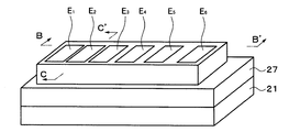
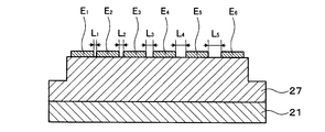
- FIGS. 12A to 12C the GaN-based semiconductor layer 27 on the C-plane sapphire substrate 21 is patterned into a predetermined shape by etching and standard lithography techniques, and then the patterned GaN-based semiconductor layer 27 is formed. Electrodes E 1 to E 6 were formed on the substrate.
- 12A is a perspective view
- FIG. 12B is a cross-sectional view taken along the line BB ′ of FIG. 12A
- FIG. 12C is a cross-sectional view taken along the line CC ′ of FIG. 12A.
- the GaN-based semiconductor layer 27 means all GaN-based semiconductor layers grown on the C-plane sapphire substrate 21.
- the etching depth of the GaN-based semiconductor layer 27 is 600 nm.
- the electrodes E 1 to E 6 are Ni / Au electrodes and have a size of 200 ⁇ m ⁇ 200 ⁇ m.
- the distance between electrodes is 7 ⁇ m for the distance L 1 between the electrodes E 1 and E 2 , 10 ⁇ m for the distance L 2 between the electrodes E 2 and E 3, and between the electrodes E 3 and E 4 .
- the distance L 3 is 15 ⁇ m
- the distance L 4 between the electrode E 4 and the electrode E 5 is 30 ⁇ m
- the distance L 5 between the electrode E 5 and the electrode E 6 is 50 ⁇ m.
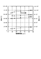
- FIG. 13 shows the measurement results of the electrical resistance with respect to the distance between the electrodes.
- the obtained slope of the straight line includes information on the resistance of the conductor layer, and the coordinate value of the intersection with the horizontal axis passing through the vertical axis includes information on contact resistance (contact resistance).
- contact resistance contact resistance
- the thickness of the p + -type GaN contact layer 26 needs to be 20 nm or more. I understood that.
- Experiment 2 Based on the results of Experiment 1, an additional Experiment 2 was performed.
- Sample 5 in which only the Mg concentration on the surface was increased was produced, and the contact resistance was measured.
- Table 2 From Table 2, according to Sample 5, it was found that increasing the concentration of the p + -type GaN contact layer 26 on the outermost surface is effective in reducing the contact resistance.
- Experiment 3 was performed to determine the necessary conditions for the polarization superjunction region.
- the hole concentration in the polarization superjunction region was measured by Hall measurement.
- the polarization superjunction element exhibits a maximum withstand voltage when the two-dimensional electron gas (2DEG) and the two-dimensional hole gas (2DHG) are generated in substantially equal amounts by the polarization effect.
- 2DEG two-dimensional electron gas
- 2DHG two-dimensional hole gas
- the excess holes derived from the Mg acceptor do not occur, the 2DEG concentration is equal to the 2DHG concentration, and no other holes exist. Therefore, such a p-type GaN layer 25 needs to be designed.
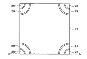
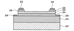
- a Ti / Al / Au electrode 28 is formed on the surface of the undoped Al x Ga 1-x N layer 23, and a Ni / Au electrode 29 is formed on the p + -type GaN contact layer 26 at the four corners inside the undoped Al x Ga 1-x N layer 23. Hole measurement for holes and hole measurement for two-dimensional electrons were made possible.
- portions other than the four corners were etched from the surface of the p + -type GaN contact layer 26 to a depth of 0 nm and 70 nm, respectively, and hole measurement was performed for holes and electrons.
- it is etched from the surface of the p + -type GaN contact layer 26 to a depth of 70 nm, in addition to the p + -type GaN contact layer 26 is also the upper part of the p-type GaN layer 25 thereunder corresponds to the removal .
- a sample having an etching amount of 0 nm is referred to as sample 6, and a sample having an etching amount of 70 nm is referred to as sample 7.
- Table 3 shows the sheet resistance value, sheet concentration, and mobility of holes (2DHG) and electrons (2DEG) of Samples 6 and 7 at room temperature.
- the hole concentration of Sample 6 with an etching amount of 0 nm was 1.12 ⁇ 10 13 cm ⁇ 2
- the electron concentration was 5.21 ⁇ 10 12 cm ⁇ 2 .
- the hole concentration slightly decreases when the p + -type GaN contact layer 26 is removed, and the p-type GaN layer 25 underneath is removed.
- the electron concentration showed a constant value of about 5.2 ⁇ 10 12 cm ⁇ 2 regardless of the etching amount.
- the hole concentration was 9.85 ⁇ 10 12 cm ⁇ 2 .
- concentration of the obtained hole is examined.
- the hole concentration is 3.0 ⁇ 10 11 cm ⁇ 2 when the room temperature activation rate of the Mg acceptor is 1.0%.
- the experimental value was 9.85 ⁇ 10 12 cm ⁇ 2 .
- the change in the two-dimensional electron concentration was hardly changed by the etching of the p + -type GaN contact layer 26 and the p-type GaN layer 25, and was about 5.3 ⁇ 10 12 cm ⁇ 2 .
- the 2DHG concentration at low temperature was 6.5 ⁇ 10 12 cm ⁇ 2 for Sample 6 with an etching amount of 0 nm, and 6.0 ⁇ 10 12 cm ⁇ 2 for Sample 7 with an etching amount of 70 nm.
- the 2DHG concentration deduced from room temperature measurement data was verified by 77K measurement.
- the hole mobility was improved by suppressing acoustic scattering, and 52 to 57 cm 2 / Vs was obtained.
- the intensity of the peak electric field depends on the quantitative balance between the 2DHG concentration and the 2DEG concentration.
- the polarization superjunction effect is effective, that is, it can be said that the polarization superjunction is a case where the 2DHG concentration is 1/10 to 1/5 of the 2DEG concentration. It is estimated that when it is less than 1/10, it is no longer different from normal HEMT.
- 1/5 of the 2DEG concentration is set as a criterion (effective limit value) of the 2DHG concentration.
- a normal AlGaN / GaN HEMT structure was prepared as a reference sample (reference sample), its 2DEG concentration was confirmed, and then the undoped GaN layer and p-type under the structural conditions of the AlGaN layer A polarization superjunction structure is produced by laminating GaN layers, and the 2DEG concentration in that case is confirmed and at the same time the 2DHG concentration is measured.
- a structure without the undoped GaN layer 24 and the p-type GaN layer 25, that is, a normal AlGaN / GaN HEMT structure was prepared for reference.
- 3 types of HEMT samples (samples A-1, A-2, A-3) were prepared and their 2DEG concentrations were measured. Table 5 shows the results.
- the 2DEG concentration slightly changed depending on the thickness of the underlying undoped GaN layer 22, but if the thickness of the undoped GaN layer 22 is 600 nm or more, the 2DEG concentration is constant at 1.1 ⁇ 10 13 cm ⁇ 2.
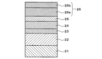
- a sample shown in FIG. 15 was prepared as a new sample. As shown in FIG. 15, this sample has the same structure as the sample 1, but the thickness of the p-type GaN layer 25 is 40 nm, and the Mg concentration of the p-type GaN layer 25 is 5 ⁇ 10 18 cm ⁇ 3 , 2 ⁇ 10 18 cm -3, 5 ⁇ 10 17 cm -3, 1 ⁇ 10 17 cm -3, changing the 0 cm -3, p + -type GaN contact layer 26, Mg concentration in the thickness 47nm is 5 ⁇ 10 19 Mg concentration lower p + -type GaN contact layer 26a and the thickness of 3nm of cm -3 were prepared 2 ⁇ 10 20 cm upper p + -type GaN contact layer 26b samples 8-12 of five configured in -3.
- a sample 13 was prepared by thinning the p-type GaN layer 25 of the sample 10 to a thickness of 20 nm by etching.
- Samples 8 to 13 were used to produce hole measurement samples as shown in FIG. 16, and hole measurement was performed by the same method as in Experiment 4.
- the results are shown in Table 6.
- the sheet electron density is approximately 5.0 ⁇ 10 12 cm ⁇ 2 to 5.3 ⁇ 10 12 cm ⁇ 2
- the standard HEMT structure samples A-1, A-2, A-3 It was reduced to about 1/2 of the above.
- the thickness of the undoped GaN layer 24 is 25 nm
- the thickness of the p-type GaN layer 25 is 20 nm
- the Mg concentrations are 2 ⁇ 10 18 cm ⁇ 3 , 5 ⁇ 10 17 cm ⁇ 3 and 0 cm ⁇ 3 , respectively.
- Three types of samples 14 to 16 were prepared. Table 7 shows the results of Hall measurement of these samples 14 to 16. From Table 7, Sample 15 and Sample 16 having a low Mg concentration had a very high resistance and it was difficult to measure the hole concentration. The electron concentration was slightly high (5.5 to 6.0) ⁇ 10 12 cm ⁇ 2 .
- the thickness of the undoped GaN layer 24 is 15 nm
- the thickness of the p-type GaN layer 25 is 15 nm
- the Mg concentrations are 2 ⁇ 10 18 cm ⁇ 3 , 5 ⁇ 10 17 cm ⁇ 3, and 0 cm ⁇ 3 , respectively.
- Three types of samples 17 to 19 were prepared. Table 8 shows the results of Hall measurement of Samples 17-19. From Table 8, Sample 18 and Sample 19 with a low Mg concentration were very high resistance and it was difficult to measure the hole concentration. The electron concentration was (5.9 to 6.8) ⁇ 10 12 cm ⁇ 2 .
- FIG. 17 shows the layer structure of the sample 20. Specifically, a GaN buffer layer (not shown) having a thickness of 30 nm is stacked on the C-plane sapphire substrate 21 by low-temperature growth (530 ° C.), and then the growth temperature is increased to 1100 ° C.
- the central portion of the p + -type GaN contact layer 26a and the p + -type GaN contact layer 26b of the sample 20 is completely etched, and the central portion of the p-type GaN layer 25 is further etched to a thickness of 10 nm.
- a sample 21 was produced.
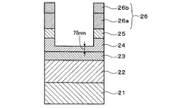
- the central portion of the p-type GaN layer 25, the p + -type GaN contact layer 26a and the p + -type GaN contact layer 26b of the sample 20 is completely etched, and the central portion of the undoped GaN layer 24 is further etched.
- the sample 22 was manufactured by setting the thickness to 75 nm. As shown in FIG.
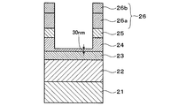
- the central portions of the p-type GaN layer 25, the p + -type GaN contact layer 26a and the p + -type GaN contact layer 26b of the sample 20 are completely etched, and the undoped GaN layer 24 is further etched to obtain a thickness.
- Sample 23 was produced by setting the thickness to 30 nm.
- Table 9 shows the results of Hall measurement using Samples 20-23. As shown in Table 9, the hole concentration of the sample 20 without etching was 9.01 ⁇ 10 12 cm ⁇ 2 , whereas the hole concentrations of the sample 21 and the sample 22 were 5.82 ⁇ 10 6 respectively. 12 cm ⁇ 2 and 5.1 ⁇ 10 12 cm ⁇ 2 . In Sample 23, the current did not flow with high resistance, and the presence of holes could not be confirmed.
- Table 10 summarizes the structures and 2DHG concentrations of Samples 7 to 23 described above.
- the sample numbers are listed in the first column, the thicknesses of the undoped GaN layer 24, the p-type GaN layer 25, and the Mg concentration of the p-type GaN layer 25 (1 ⁇ in the second to fourth columns). 10 18 cm -3 as a unit).
- the measured 2DHG concentration is shown in the sixth column.
- the fifth column is a value based on a new concept of “reduced thickness”, which is a new index introduced to organize experimental values.
- the converted thickness will be described.
- the converted thickness is expressed as tR.
- the converted thickness tR is an amount represented by the following formula.
- the thickness of the undoped GaN layer 24 is represented by u [nm]
- the thickness of the p-type GaN layer 25 is represented by v [nm]
- the Mg concentration is represented by w [cm ⁇ 3 ]
- the meaning of the term on the right side of this equation will be described.
- the p-type GaN layer 25 has a higher band than the undoped GaN layer 24 with respect to the Fermi level.
- the effect of the band at the surface side AlGaN / GaN heterojunction interface rising and generating 2DHG is greater in the p-type GaN layer 25 than in the undoped GaN layer 24. Therefore, the effect of the Mg dopant in the p-type GaN layer 25 will be considered.
- the activation rate of Mg dopant at room temperature is about 1%.
- deep levels and n-type impurities are present in the GaN layer from 10 16 cm ⁇ 3 to 10 17 cm ⁇ 3 , which hinders the role of Mg as an acceptor. Therefore, the Mg concentration on the order of 10 17 cm ⁇ 3 does not play a significant role as p-type.
- the Mg concentration is lower than 10 17 cm ⁇ 3 , it is closer to the undoped layer. Therefore, when evaluating the contribution of the p-type GaN layer 25 to the 2DHG concentration of this structure, it is necessary to incorporate the effect thereof, which can be given by setting 10 18 cm ⁇ 3 as a normalized value. From the above consideration, it is derived as a first order approximation. Accordingly, the 2DHG concentration is expected to have a linear relationship and a saturation curve thereafter with respect to the converted thickness tR represented by the equation (1).
- the fifth column of Table 10 shows the converted thickness tR calculated by Equation (1).
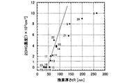
- FIG. 21 shows the converted thickness tR in the fifth column of Table 10 on the x-axis and the 2DHG concentration in the sixth column on the y-axis.
- FIG. 22 shows an enlarged view of a region where the converted thickness tR is 20 to 90 nm in FIG.
- the numerical values in FIGS. 21 and 22 indicate sample numbers.
- FIG. 21 it was found that the 2DHG concentration is roughly proportional to the converted thickness tR, and when the converted thickness tR increases, the 2DHG concentration tends to saturate around 1 ⁇ 10 13 cm ⁇ 2 . In the region where the 2DHG concentration is small (FIG.
- the measurement error of the Hall measurement becomes large and varies slightly, but it was confirmed that the 2DHG concentration is approximately proportional to the converted thickness tR.
- the converted thickness tR was 50 nm or less, the hole concentration could not be measured.
- the reason why the error of hole measurement becomes large is that the hole mobility is as small as ⁇ 1 / 100 of that of the electron, so that the measured Hall voltage is small, and the p-type GaN layer 25 This is because the contact resistance value of the ohmic electrode is inherently high (experimentally, 10 5 times the contact resistance value of the ohmic electrode to the n-type GaN layer).
- the 2DEG concentration was approximately 1.1 ⁇ 10 13 cm ⁇ 2 (see Table 5).
- the 2DEG concentration in the case of this polarization superjunction structure was approximately (5.1 to 6.8) ⁇ 10 12 cm ⁇ 2 throughout the samples 8 to 23.
- This undoped Al x Ga 1-x with a relatively thick undoped GaN layer 24 and p-type GaN layer 25 band lifting effect on the N layer 23, an undoped Al x Ga 1-x N layer 23 and the undoped GaN layer 22 This is because the 2DEG concentration of the lower AlGaN / GaN heterojunction formed by the above is reduced.
- the 2DEG concentration increases with a decrease as the converted thickness tR is smaller, that is, as the band lift is smaller. Nevertheless, interestingly, for the combined change of the upper undoped GaN layer 24 and the p-type GaN layer 25, the almost constant 2DEG concentration (5.1 to 6.8) ⁇ 10 12 cm ⁇ 2 is obtained. Pay attention to those who are.
- the 2DEG concentration in the case of this polarization superjunction structure is about 1 ⁇ 2 of the 2DEG concentration of the reference HEMT.
- the 2DEG concentration of the reference HEMT can define the lower limit (limit 2DHG concentration) of the effective 2DHG concentration of the polarization superjunction structure having the corresponding undoped Al x Ga 1-x N layer 23. . That is, the 2DEG concentration of this reference HEMT structure can be used as a reference.
- the effective 2DHG concentration needs to be about 1/10 to 1/5 or more of the 2DEG concentration.
- the above-described effective range of the converted thickness tR is obtained when the Al composition x of the undoped Al x Ga 1-x N layer 23 is 0.23 and the thickness is 47 nm. What happens when the Al composition and thickness are different from the above?
- Sample A-3 is a sample already described.
- Sample A-4 has an Al composition x of 0.17 and a thickness of 47 nm
- Sample A-5 has an Al composition x of 0.37 and a thickness of 47 nm
- Sample A-6 has an Al composition x of 0.1. 37 and the thickness is 25 nm.
- cracks were generated in the crystal, and the film was torn, making measurement impossible.
- FIG. 23 shows a known document (F. Calle et al. Journal of Materials Science: Materials in Electronics) showing the relationship between the Al composition x of the Al x Ga 1-x N layer and the sheet carrier concentration (2DEG concentration). 14 (2003) 271-277) p. 272 FIG.
- FIG. 1 shows data ( ⁇ , ⁇ , ⁇ ) of samples A-3, A-4, and A-6.
- the Al composition x of the Al x Ga 1-x N layer is changed from 0.16 to 0.36 and the thickness is changed from 17 nm to 42 nm.
- the 2DEG concentration increases in proportion to the Al composition, and with respect to the thickness, the strain increases as the thickness increases. However, the 2DEG concentration tends to increase, but does not increase significantly.
- the 2DEG concentrations of Samples A-3, A-4, and A-6 are relatively higher than the literature values.
- an undoped GaN layer 24 having a thickness of 80 nm and a p-type GaN layer having a thickness of 40 nm and an Mg concentration of 1 ⁇ 10 18 cm ⁇ 3.
- Mg concentration thickness at 44nm is 5 ⁇ 10 19 cm p + -type GaN layer 26a and the thickness of -3 is Mg concentration 3nm laminating p + -type GaN layer 26b of 2 ⁇ 10 20 cm -3
- sample 24 was produced.
- the sample 25 was fabricated by etching the p-type GaN layer 25 of the sample 24 to a thickness of 20 nm.
- the undoped GaN layer 24 was etched to a depth of 5 nm, and the sample 26 was manufactured with a thickness of 75 nm. Further, the p-type GaN layer 25 of the sample 24 was completely removed by etching, and then the undoped GaN layer 24 was etched to a depth of 30 nm to prepare a sample 27 with a thickness of 50 nm. Table 12 shows the results of Hall measurement of these samples 24-27. The hole concentration of sample 27 could not be measured.
- the 2DEG concentration increased as the thickness of the undoped GaN layer 24 decreased, and was (3.8 to 4.1) ⁇ 10 12 cm ⁇ 2 . This 2DEG concentration was 42% to 46% of the 2DEG concentration of sample A-4, 8.9 ⁇ 10 12 cm ⁇ 2 .
- an undoped GaN layer 24, a p-type GaN layer 25, a p + -type GaN layer 26a and a p + -type GaN layer 26b similar to those of the sample 24 are stacked to obtain a sample having a polarization superjunction structure. 28 was produced.
- a sample 29 in which the thickness of the p-type GaN layer 25 is 20 nm, a sample 30 in which the thickness of the undoped GaN layer 24 is 75 nm, and a sample 31 in which the thickness of the undoped GaN layer 24 is 46 nm are manufactured by etching. did. Table 13 shows the results of Hall measurement of these samples 28 to 31.
- FIG. 24 is an enlarged view of a portion where the converted thickness tR in FIG. 24 is 0 to 150 nm in order to estimate the limit converted thickness tR at which the device operates.
- the value of 1/10 of the 2DEG concentration of the reference samples A-3, A-4, and A-6, that is, the limit 2DHG concentration is indicated by a horizontal line. That is, the limit 2DHG concentration is 1.1 ⁇ 10 12 cm ⁇ 2 in sample A-3, 0.89 ⁇ 10 12 cm ⁇ 2 in sample A-4, and 1.7 ⁇ 10 12 cm ⁇ in sample A-6. 2 .
- This limit 2DHG concentration is the minimum 2DHG concentration necessary for the device to operate as a polarization superjunction device.
- the 2DHG concentration effective as a polarization superjunction element is important to balance with the 2DEG concentration, and the value is 1/5 to 1/10 of the concentration of coexisting 2DEG. However, 1/5 in the direction of higher density (stricter one) is adopted here.
- the converted thickness tR reaching the limit 2DHG concentration is 0.17 for the Al composition of the undoped Al x Ga 1-x N layer 23, 70 nm for the samples 24 to 27 having a thickness of 47 nm, and the Al composition is 0.1.
- Samples 8 to 23 having a thickness of 47 nm 55 nm was obtained, and in Samples 28 to 31 having an Al composition of 0.35 and thickness of 25 nm, 50 nm was obtained.
- the limit thickness was 55 nm from FIG.
- the thickness of the undoped Al x Ga 1-x N layer of the sample having an Al composition x of 0.35 is 25 nm. As shown in FIG. 23, in the region of this thickness (from 17 nm to 42 nm), the 2DEG concentration is 2DEG. The thickness dependence is about 30% at most. Especially in the range of the thickness of the experiment (25 nm to 47 nm), the limit thickness of the three sample groups can be understood as a difference in Al composition.
- FIG. 26 is a plot of the converted thickness tR against the limit 2DHG concentration against the Al composition x of the undoped Al x Ga 1-x N layer 23.
- the three data in FIG. 26 are the limit conversion thickness for each Al composition x.
- FIG. 26 shows a curve passing through these three points. This curve is given by the following formula (3) where the Al composition is x and the limit thickness is y [nm].
- y a / (x ⁇ b) + c (3)
- This formula (3) is an empirical formula adopted to give a limit thickness to a structure in which the Al composition x of the undoped Al x Ga 1-x N layer 23 is different.
- the converted thickness tR is expressed by the formula (3). It must be greater than the critical thickness shown. That is, in the range where the Al composition is 0.17 to 0.35 and the thickness is 25 nm to 47 nm, the applied equivalent thickness tR is tR ⁇ 0.864 / (x ⁇ 0.134) +46.0 [nm] (4) It is.
- a polarization superjunction region and a p-electrode contact region are structurally separated, and a p + -type GaN contact having an acceptor concentration (Mg concentration) higher than that of the p-type GaN layer 25 in the p-electrode contact region.
- Mg concentration acceptor concentration
- the polarization superjunction region and the p-electrode contact region may be formed using a method as shown in FIG. 27 or FIG. 28A and FIG. 28B. That is, as shown in FIG. 27, after growing to the p-type GaN layer 25, a growth mask 30 made of a dielectric film such as a SiO 2 film is formed thereon, and a part of this growth mask 30 is etched.
- An opening is formed by removing, and ap + -type GaN contact layer 26 is selectively grown on the p-type GaN layer 25 exposed in the opening.
- a growth mask 30 made of a dielectric film such as a SiO 2 film is formed thereon, and a part of the growth mask 30 is etched.
- An opening is formed by removal, and the groove 31 is formed by etching to an intermediate depth of the undoped Al x Ga 1-x N layer 23 using the growth mask 30.
- a p + -type GaN contact layer 26 is selectively grown and buried in the groove 31 using a growth mask 30.
- FIG. 29 shows a field effect transistor having a four-terminal structure.
- an undoped GaN layer 41, an undoped Al x Ga 1-x N layer 42 (0.17 ⁇ x ⁇ 0.35) having a thickness of 25 nm to 47 nm, an undoped GaN layer 43, and p-type GaN Layers 44 are sequentially stacked.
- the undoped GaN layer 43 and the p-type GaN layer 44 on the undoped Al x Ga 1-x N layer 42 are patterned in a mesa shape, and a p + -type GaN contact layer 45 is provided in a mesa shape on the p-type GaN layer 44. Yes.
- a source electrode 46 and a drain electrode 47 are provided on the undoped Al x Ga 1-x N layer 42 with the undoped GaN layer 43 and the p-type GaN layer 44 interposed therebetween.
- the source electrode 46 and the drain electrode 47 are made of, for example, a Ti / Al bilayer film and are in ohmic contact with the undoped Al x Ga 1 -x N layer 42.
- a gate electrode 48 is provided on the undoped Al x Ga 1-x N layer 42 between the source electrode 46 and the undoped GaN layer 43 and the p-type GaN layer 44, and a p - electrode is formed on the p + -type GaN contact layer 45. 49 is provided.
- the gate electrode 48 is made of, for example, a Ni / Au bilayer film, and is in Schottky contact with the undoped Al x Ga 1-x N layer 42.
- the p electrode 49 is formed of, for example, a Ni / Au bilayer film and is in ohmic contact with the p + -type GaN contact layer 45.
- This field effect transistor has a method of connecting the p electrode 49 and the source electrode 46 (this corresponds to a metal field plate (FP) source field plate) and a method of connecting the p electrode 49 and the gate electrode 48 ( If the p-electrode 49 is considered as a base electrode, this corresponds to a base field plate).
- FP metal field plate
- FIG. 30 shows a field effect transistor having a three-terminal structure.
- an undoped GaN layer 41, an undoped Al x Ga 1-x N layer 42, an undoped GaN layer 43, and a p-type GaN layer 44 are sequentially stacked.
- the undoped GaN layer 43 and the p-type GaN layer 44 on the undoped Al x Ga 1-x N layer 42 are patterned in a mesa shape, and a p + -type GaN contact layer 45 is provided in a mesa shape on the p-type GaN layer 44. Yes.
- a source electrode 46 and a drain electrode 47 are provided on the undoped Al x Ga 1-x N layer 42 with the undoped GaN layer 43 and the p-type GaN layer 44 interposed therebetween.
- the gate electrode 48 that also serves as the p-electrode 49 is formed on the undoped GaN layer 43 and the p-type. It is provided to extend over the p + -type GaN contact layer 45 from the end surface of the GaN layer 44.
- the gate electrode 48 is made of, for example, a Ni / Au bilayer film and is in ohmic contact with the p + -type GaN contact layer 45.
- This field effect transistor has a three-terminal structure in which the gate electrode 48 and the p electrode 49 are integrated, and is equivalent to the field effect transistor shown in FIG. 25 in which the gate electrode 48 and the p electrode 49 are integrated. .
- FIG. 31 shows a normally-off type three-terminal field effect transistor.
- an undoped GaN layer 41, an undoped Al x Ga 1-x N layer 42, an undoped GaN layer 43, and a p-type GaN layer 44 are sequentially stacked.
- the undoped GaN layer 43 and the p-type GaN layer 44 on the undoped Al x Ga 1-x N layer 42 are patterned in a mesa shape, and a p + -type GaN contact layer 45 is provided in a mesa shape on the p-type GaN layer 44. Yes.
- a source electrode 46 and a drain electrode 47 are provided on the undoped Al x Ga 1-x N layer 42 with the undoped GaN layer 43 and the p-type GaN layer 44 interposed therebetween.
- a groove is provided in the undoped Al x Ga 1-x N layer 42 between the source electrode 46 and the undoped GaN layer 43 and the p-type GaN layer 44 so as to continue to the end faces of the undoped GaN layer 43 and the p-type GaN layer 44.
- the gate electrode 48 that also serves as the p electrode 49 is embedded in the groove, and further extends on the p + -type GaN contact layer 45 from the end faces of the undoped GaN layer 43 and the p-type GaN layer 44.
- the threshold voltage of the field effect transistor is controlled by controlling the thickness of the undoped Al x Ga 1-x N layer 42 in the groove portion provided in the undoped Al x Ga 1-x N layer 42 or the etching residue when the groove is formed. Do by quantity.
- FIG. 32 shows a field effect transistor having a three-terminal structure.
- an undoped GaN layer 41, an undoped Al x Ga 1-x N layer 42, an undoped GaN layer 43, and a p-type GaN layer 44 are sequentially stacked.
- the undoped GaN layer 43 and the p-type GaN layer 44 on the undoped Al x Ga 1-x N layer 42 are patterned in a mesa shape, and a p + -type GaN contact layer 45 is provided in a mesa shape on the p-type GaN layer 44. Yes.
- a source electrode 46 and a drain electrode 47 are provided on the undoped Al x Ga 1-x N layer 42 with the undoped GaN layer 43 and the p-type GaN layer 44 interposed therebetween.
- a p-electrode 49 that also serves as the gate electrode 48 is provided on the p + -type GaN contact layer 45. The operation of this field effect transistor is the same as that of the field effect transistor shown in FIG. 31 except that the threshold voltage is deep (shifted to the negative side).
- FIG. 33 shows a normally-off type three-terminal field effect transistor.
- an undoped GaN layer 41, an undoped Al x Ga 1-x N layer 42, an undoped GaN layer 43, and a p-type GaN layer 44 are sequentially stacked.
- the undoped GaN layer 43 and the p-type GaN layer 44 on the undoped Al x Ga 1-x N layer 42 are patterned in a mesa shape.
- a groove is provided in the undoped Al x Ga 1-x N layer 42 so as to continue to the end faces of the undoped GaN layer 43 and the p-type GaN layer 44, and a p + -type GaN contact layer 45 is embedded in the groove, and this p The + -type GaN contact layer 45 and a two-dimensional hole gas (not shown) are joined.
- the p + -type GaN contact layer 45 can be grown by selective regrowth.
- a source electrode 46 and a drain electrode 47 are provided on the undoped Al x Ga 1-x N layer 42 with the undoped GaN layer 43 and the p-type GaN layer 44 interposed therebetween.
- a p-electrode 49 that also serves as the gate electrode 48 is provided on the p + -type GaN contact layer 45.
- the gate electrode 48 is a Schottky junction type, but in this field effect transistor, the gate electrode 48 is a p / n junction type.
- the gate electrode 48 of this field effect transistor is a p / n junction type, but the diffusion potential of the p / n junction is 3.4 V, which is +2 V higher than the diffusion potential of the Schottky junction ⁇ 1.4 V, The gate threshold voltage can be increased.
- an undoped Al x Ga 1-x N layer 42 of the lower portion of the p + -type GaN contact layer 45 is completely removed, even contacting the p + -type GaN contact layer 45 on the undoped GaN layer 41, improving the threshold voltage It is a good structure from the viewpoint.
- FIG. 34 shows a diode having a three-terminal structure.
- an undoped GaN layer 51 an undoped Al x Ga 1-x N layer 52, an undoped GaN layer 53, and a p-type GaN layer 54 are sequentially stacked.
- the undoped GaN layer 53 and the p-type GaN layer 54 on the undoped Al x Ga 1-x N layer 52 are patterned in a mesa shape, and a p + -type GaN contact layer 55 is provided in a mesa shape on the p-type GaN layer 54. Yes.
- An anode electrode 56 and a cathode electrode 57 are provided across the undoped GaN layer 53 and the p-type GaN layer 54.
- the anode electrode 56 is embedded in a groove 58 provided at a depth reaching the undoped GaN layer 51, and is a portion in the vicinity of the heterointerface between the undoped GaN layer 51 and the undoped Al x Ga 1-x N layer 52.
- the anode electrode 56 is formed of, for example, a Ni / Au bilayer film that is in Schottky contact with an n-type GaN-based semiconductor.
- the source electrode 57 is provided on the undoped Al x Ga 1-x N layer 52.
- a p-electrode 59 is provided on the p + -type GaN contact layer 55.
- the anode electrode 56 and the p electrode 59 are electrically connected to each other.
- This diode has a Schottky junction formed by etching the undoped Al x Ga 1-x N layer 52 below the gate electrode 48 of the field effect transistor shown in FIG. 25 and bringing it into contact with the undoped GaN layer 51. Equivalent to. If necessary, the anode electrode 56 and the p electrode 59 may be integrally formed.
- FIG. 35 shows a diode having a two-terminal structure.
- an undoped GaN layer 51 an undoped Al x Ga 1-x N layer 52, an undoped GaN layer 53, and a p-type GaN layer 54 are sequentially stacked.
- the undoped GaN layer 53 and the p-type GaN layer 54 on the undoped Al x Ga 1-x N layer 52 are patterned in a mesa shape.
- a groove is provided in the undoped Al x Ga 1-x N layer 52 so as to continue to the end faces of the undoped GaN layer 53 and the p-type GaN layer 54, and a p + -type GaN contact layer 55 is embedded in the groove, and this p The + -type GaN contact layer 55 and a two-dimensional hole gas (not shown) are joined.
- An anode electrode 56 and a cathode electrode 57 are provided across the undoped GaN layer 53 and the p-type GaN layer 54.
- Another groove 58 having a depth reaching the undoped GaN layer 51 is provided continuously to the p + -type GaN contact layer 55.
- the anode electrode 56 is embedded in the other groove 58 and further extends on the p + -type GaN contact layer 55.
- the anode electrode 56 is formed of, for example, a Ni / Au bilayer film.
- the source electrode 57 is provided on the undoped Al x Ga 1-x N layer 52.
- FIG. 36 shows a diode having a two-terminal structure.
- an undoped GaN layer 51 an undoped Al x Ga 1-x N layer 52, an undoped GaN layer 53, and a p-type GaN layer 54 are sequentially stacked.
- the undoped GaN layer 53 and the p-type GaN layer 54 on the undoped Al x Ga 1-x N layer 52 are patterned in a mesa shape, and a p + -type GaN contact layer 55 is provided in a mesa shape on the p-type GaN layer 54. Yes.
- a groove 60 is provided in the undoped Al x Ga 1-x N layer 52 between the anode electrode 56 and the undoped GaN layer 53 and the p-type GaN layer 54 so as to continue to the end surfaces of the undoped GaN layer 53 and the p-type GaN layer 54. It has been.
- a p-electrode 59 is embedded in the groove 60, and extends from the end faces of the undoped GaN layer 53 and the p-type GaN layer 54 onto the p + -type GaN contact layer 55, and is electrically connected to the anode electrode 56 together. Connected.
- This diode has a structure in which a source electrode 46 and a gate electrode 48 of a normally-off (enhancement mode) field effect transistor having a gate threshold voltage of 0 V or more shown in FIG. 32 are integrated.
- a positive voltage is applied to the anode electrode 56 with respect to the cathode electrode 57, the Schottky junction is turned on, and a forward current flows between the anode electrode 56 and the cathode electrode 57, which are ohmic electrodes.
- a negative voltage is applied to the anode electrode 56, the Schottky junction is turned off, and no current flows between the anode electrode 56 and the cathode electrode 57 that are adjacent to each other.
- an undoped GaN layer 61, an undoped Al x Ga 1-x N layer 62, an undoped GaN layer 63, and a p-type GaN layer 64 are sequentially stacked.
- the undoped GaN layer 63 and the p-type GaN layer 64 on the undoped Al x Ga 1-x N layer 62 are patterned in a mesa shape.
- a source electrode 65 and a drain electrode 66 are provided on the undoped Al x Ga 1-x N layer 62 with the undoped GaN layer 63 and the p-type GaN layer 64 interposed therebetween.
- FIG. 37 shows the state of electrons and holes when the transistor is on.
- Reference numeral 68 indicates 2DHG
- 69 indicates 2DEG.
- FIG. 38 shows the state of electrons and holes when the transistor is off. In FIG. 38, a negative voltage is applied to the gate electrode 67, holes (2DHG 68) are extracted through the gate electrode 67, and the electron channel (2DEG 69) immediately below the holes is depleted. In this manner, holes (2DHG68) are injected / extracted in the on / off operation of the transistor. If there is an obstacle to the movement of holes (2DHG68), the dynamic characteristics are affected.
- Factors affecting the movement of holes include hole mobility. As shown in Table 3, the hole mobility is about 15 to 30 [cm 2 / Vs] experimentally. This value is 1/500 to 1/1000 of the electron mobility, and it is considered that the hole movement speed dominates the speed of this transistor. Then, the switching speed is estimated to be 1/1000 or less of a normal HFET. Therefore, although it depends on the length of the polarization superjunction region, the cutoff frequency is estimated to be about several MHz to several tens of MHz. However, the switching frequency of Si-IGBT (Insulated Gate Bipolar Transistor) is at most several tens of kHz, and that of Si-power MOSFET is several MHz. This field effect transistor using a superjunction is applied to a high voltage power device, and the speed can be higher than that of Si-IGBT and Si-power MOSFET.
- Si-IGBT Insulated Gate Bipolar Transistor
- the transistor 2 since the high concentration p + -type GaN contact layer 71 is added to the outermost surface, the p + -type GaN contact layer 71 other than the contact region of the gate electrode 67 that also serves as the p electrode is removed by etching. .
- the etching amount is 60 nm.
- the contact resistance of the transistor 1 is 1.3 ⁇ 10 4 ⁇ cm 2, the contact resistance of the transistor 2 is 0.84Omucm 2.
- the measurement circuit is shown in FIG. As shown in FIG. 41, a DC voltage source, a load resistor, and a test transistor (transistor 1 or 2) were connected in series. The power supply voltage was set to 200V and the load resistance was set to 392 ⁇ . The transistor 1 or 2 was held for 10 seconds in a pinch-off state, and then a positive voltage pulse was applied to the gate electrode 67 to turn on the transistor 1 or 2. The pulse width of the positive voltage applied to the gate electrode 67 is 1 ⁇ s.
- the transistor 1 or 2 which is a PSJ-FET is indicated by a symbol. In this symbol, ⁇ indicates 2DHG.
- the drain voltage V d shows waveforms of the gate voltage V g , the drain voltage V d , and the drain current I d .
- a voltage is applied to the load resistance, so that the drain voltage V d decreases.
- the transistor 1 has a constant value with no further drop in V d .
- the V d value that reached a constant value was 69V. This indicates that the channel resistance of the element is very large, which is a so-called current collapse state. This phenomenon is called switching collapse, and this is a big problem even in a normal HFET.
- the cause of this is that the hole injection rate is low, the region of the p-type GaN layer 64 remains in a negative ionization state, channel constriction occurs due to the Coulomb effect, a small drain current I d and a large drain voltage V. The state d is generated. In the transistor 1 as well, current collapse is eliminated at DC (pulse width of several hundred ms or more).
- the transition from the on state to the off state results in a very high reverse bias state of 200 V between the gate electrode 67 and the drain electrode 66, so that the contact resistance of the gate electrode 67 that also serves as the p electrode to the p-type GaN layer 64 is reduced. It can be seen that even if it is high, holes are drawn out and a clean off state is achieved at a speed of 100 ns or less.
- the trade-off relationship between high breakdown voltage and high speed in the semiconductor element using the polarization superjunction proposed in Patent Document 3 and Non-Patent Document 3 is easily broken down.
- Second Embodiment> A GaN-based semiconductor device according to the second embodiment will be described.
- the critical conversion thickness is obtained with respect to the structure (composition / thickness) of the undoped Al x Ga 1-x N layer 23 (or the undoped Al x Ga 1-x N layer 12). .
- the structure of the Al x Ga 1-x N layer and the 2DEG concentration have a primary relationship as described in the above-mentioned reference, and the relationship between the converted thickness tR and the 2DEG concentration of the reference HEMT.
- the reference HEMT has a structure composed of an undoped GaN layer 11 and an undoped Al x Ga 1-x N layer 12 (0.17 ⁇ x ⁇ 0.35) having a thickness of 25 nm or more and 47 nm or less formed thereon.
- the HEMT has a structure having a 2DEG concentration of 0.89 ⁇ 10 13 cm ⁇ 2 or more and 1.70 ⁇ 10 13 cm ⁇ 2 or less.
- FIG. 44 shows the converted thickness tR that gives the limit 2DHG concentration of the corresponding polarization superjunction structure with respect to the 2DEG concentration of the reference HEMT.
- FIG. 44 shows a 1 / x curve corresponding to the measured value.
- the 2DEG concentration of the reference HEMT is expressed as n S in units of 10 12 cm ⁇ 2 , and the limit conversion thickness is expressed as y.
- y a / (n S ⁇ b) + c (5)
- the Al composition x of the undoped Al x Ga 1-x N layer 12 is 0.17 ⁇ x ⁇ 0.35 and the thickness is 25 nm or more and 47 nm or less, but depending on various conditions of crystal growth,
- An undoped Al x Ga 1-x N layer 23 (or an undoped Al x Ga 1-x N layer 12 of a reference HEMT having a 2DEG concentration of 0.89 ⁇ 10 13 cm ⁇ 2 or more and 1.7 ⁇ 10 13 cm ⁇ 2 or less. )
- Structure composition / thickness can vary.
- the above 2DEG concentration can also be obtained by an undoped Al x Ga 1-x N layer 23 having an Al composition x of 0.17 ⁇ x ⁇ 0.35 and an Al composition and thickness different from the thickness of 25 nm to 47 nm. This is evident as the 2DEG concentration difference between the above reference and the reference HEMT. Because, 2DEG is because caused by polarization, the undoped Al x Ga 1-x N layer 23 is introduced to produce the polarization, the undoped Al x Ga 1-x N layer 23 to obtain the polarization degree This is because the structure (composition / thickness) can change depending on various conditions such as the growth apparatus and temperature.
- the 2DEG concentration of the reference HEMT is 0.89 ⁇ 10 13 cm ⁇ 2 or more and 1.7 ⁇ 10 13 cm ⁇ 2 or less.
- the equivalent thickness tR applicable to the undoped Al x Ga 1-x N layer 23 (0 ⁇ x ⁇ 1) is tR ⁇ 24.2 / (n S ⁇ 7.83) +47.4 [nm] (6) It is.
- a donor (n-type impurity) is used instead of the undoped Al x Ga 1-x N layer 23.
- an n-type or p-type Al x Ga 1-x N layer doped with an acceptor (p-type impurity), for example, an n-type Al x Ga 1-x N layer doped with Si may be used.
- the Mg concentration w [cm ⁇ 3 ] of the GaN layer 14 and the Al composition and thickness of the undoped Al x Ga 1-x N layer 12 (or the doped Al x Ga 1-x N layer 12) are selected. By doing so, 2DHG 16 having a concentration of 1 ⁇ 10 12 cm ⁇ 2 or more can be generated.
- this GaN-based semiconductor element is the same as the GaN-based semiconductor element according to the first embodiment.
- GaN-based semiconductor element is basically the same as that in the first embodiment.
- FIG. 45 shows this GaN-based bidirectional field effect transistor.
- an undoped GaN layer 41, an undoped Al x Ga 1-x N layer 42, an undoped GaN layer 43, and a p-type GaN layer 44 are sequentially stacked.
- the undoped GaN layer 43 and the p-type GaN layer 44 on the undoped Al x Ga 1-x N layer 42 are patterned in a mesa shape.
- two p + -type GaN contact layers 45a and 45b are mesa-type and separated from each other.
- Two source electrodes 46 a and 46 b are provided on the undoped Al x Ga 1-x N layer 42 with the undoped GaN layer 43 and the p-type GaN layer 44 interposed therebetween.
- p + -type GaN contact layer 45a is p-electrode 49a used as a gate electrode is provided
- a p-electrode 49b which is used as a gate electrode on the p + -type GaN contact layer 45b is provided.
- the source electrodes 46a and 46b, the p + -type GaN contact layers 45a and 45b, and the p-electrodes 49a and 49b are formed symmetrically with respect to the undoped GaN layer 43 and the p-type GaN layer 44.
- This GaN-based bidirectional field effect transistor turns on / off the voltage in both forward and reverse directions with respect to the input AC voltage by the signal voltage (switch signal) applied to the p electrodes 49a and 49b used as the gate electrodes. Can do.
- the source electrode 46a or the source electrode 46b functions as a drain electrode depending on the polarity of the input AC voltage.
- This GaN-based bidirectional field effect transistor is suitable for use as a bidirectional switch of a matrix converter.
- FIG. FIG. 46 shows a power supply circuit of a three-phase AC induction motor M using a matrix converter C. As shown in FIG. 46, the matrix converter C intersects each intersection of the horizontal wirings W 1 , W 2 , W 3 and the vertical wirings W 4 , W 5 , W 6 at each intersection. Bidirectional switches S for connecting the horizontal wiring and the vertical wiring are provided in a matrix. The voltages of each phase of the three-phase AC power supply P are input to the wirings W 1 , W 2 , and W 3 through the input filter F. The wirings W 4 , W 5 , W 6 are connected to the three-phase AC induction motor M. As the bidirectional switch S, a GaN-based bidirectional field effect transistor shown in FIG. 45 is used.
- the bidirectional switch S of the matrix converter C is turned on / off at high speed to directly apply the voltage of each phase of the three-phase AC input to the wirings W 1 , W 2 , W 3. Then, a three-phase AC induction motor M is driven by cutting out into strips by pulse width modulation (PWM) and outputting an AC voltage of any voltage and frequency obtained thereby to the wirings W 4 , W 5 , W 6 .
- PWM pulse width modulation
- This GaN-based bidirectional field effect transistor is also suitable for use as a bidirectional switch of a multilevel inverter.
- Multi-level inverters are effective, for example, in improving the power conversion efficiency of power conversion systems (see, for example, Fuji Time Report, Vol. 83 No. 6 2010, pp. 362-365).
- the gate electrode is switched as compared with a GaN-based field effect transistor that is not configured bidirectionally, for example, the GaN-based field effect transistor shown in FIG.
- the rise time when a signal is input can be shortened, and high-speed operation can be achieved. Therefore, by using this GaN-based bidirectional field effect transistor for the bidirectional switch S of the matrix converter C shown in FIG. 46, the bidirectional switch S can be switched at a higher speed, and the matrix converter C can be operated at a higher speed. Can be achieved.
- a high performance matrix converter C can be realized, and by using this matrix converter C, a high performance AC power supply circuit can be realized.
- a high-performance multilevel inverter can be realized, and a highly efficient power conversion system can be realized by using this multilevel inverter.
- a GaN-based bidirectional field effect transistor according to a fourth embodiment will be described.
- This GaN-based bidirectional field effect transistor has the same configuration as that of the GaN-based bidirectional field effect transistor according to the third embodiment except that Expression (5) is satisfied. Similar to the GaN-based bidirectional field effect transistor according to the third embodiment, this GaN-based bidirectional field effect transistor is used as the bidirectional switch S of the matrix converter C shown in FIG. 46 or the bidirectional switch of the multilevel inverter. be able to.
- a mounting structure in which a chip constituting a GaN-based field effect transistor or a GaN-based bidirectional field effect transistor according to any of the first to fourth embodiments is flip-chip mounted on a mounting substrate Explain the body.
- FIG. 48 shows the dependence of the off breakdown voltage of the field effect transistor (PSJ-FET) manufactured on a sapphire substrate on the length of the polarization superjunction region (PSJ length (L psj )).
- This field effect transistor has substantially the same structure as the field effect transistor shown in FIG.
- a p + -type GaN contact layer 45 is provided in a mesa shape on the p-type GaN layer 44, but is not shown in FIG.
- the p electrode 49 also serving as a gate electrode extends from the end surfaces of the undoped GaN layer 43, the p-type GaN layer 44, and the p + -type GaN contact layer 45 onto the p + -type GaN contact layer 45.
- the PSJ length L psj is between the end surface on the drain electrode 47 side of the p electrode 49 that also serves as the gate electrode and the end surface on the drain electrode 47 side of the undoped GaN layer 43 and the p-type GaN layer 44.
- Reference numeral 40 denotes a sapphire substrate.
- L psj field effect transistors
- the off breakdown voltage is proportional to L psj , and the effect of super junction is realized. Since the breakdown voltage is proportional to L psj , if the breakdown voltage is to be doubled, L psj may be doubled.
- FIG. 49 shows this field effect transistor.
- This field effect transistor has substantially the same structure as the field effect transistor shown in FIG. As shown in FIG. 49, in this field effect transistor, an AlN layer 81 having a thickness of 100 nm, an AlGaN buffer layer 82 having a thickness of 1.5 ⁇ m, and an undoped GaN layer having a thickness of 2.5 ⁇ m on a Si substrate 80.
- an undoped Al 0.23 Ga 0.77 N layer 84 having a thickness of 40 nm, an undoped GaN layer 85 having a thickness of 30 nm, and a p-type GaN layer 86 having an acceptor concentration of 1 ⁇ 10 19 cm ⁇ 3 and a thickness of 20 nm are sequentially stacked.
- the undoped GaN layer 85 and the p-type GaN layer 86 on the undoped Al 0.23 Ga 0.77 N layer 84 are patterned into a mesa shape, and the acceptor concentration is 1 ⁇ 10 20 cm ⁇ 3 and the thickness is 5 nm on the p-type GaN layer 86.
- a p + -type GaN contact layer 87 is provided in a mesa shape.
- a source electrode 88 and a drain electrode 89 are provided on the undoped Al 0.23 Ga 0.77 N layer 84 with the undoped GaN layer 85 and the p-type GaN layer 86 interposed therebetween.
- the undoped GaN layer 85 extends so that both end surfaces thereof are in contact with the source electrode 88 and the drain electrode 89, respectively.
- a p-electrode 90 also serving as a gate electrode is provided on the p + -type GaN contact layer 87.
- 2DHG15 is formed in the undoped GaN layer 85 in the vicinity of the heterointerface between the undoped Al 0.23 Ga 0.77 N layer 84 and the undoped GaN layer 85, and the undoped GaN layer 83, the undoped Al 0.23 Ga 0.77 N layer 84, 2DEG 16 is formed in the undoped GaN layer 83 in the vicinity of the hetero interface between the two.
- FIG. 50 shows the measurement results of the drain current-drain voltage characteristics of this field effect transistor (PSJ-FET).
- the gate voltage V g -10V.
- the vertical axis in FIG. 50 is a logarithmic scale.
- the drain current increases from around 800V.
- FIG. 51 shows a linear scale on the vertical axis of FIG. From FIG. 51, it can be seen that the drain current increases rapidly from around 950V. That is, the off breakdown voltage of the field effect transistor (PSJ-FET) on the Si substrate 80 is about 950 V, which is smaller than the off breakdown voltage of the field effect transistor on the sapphire substrate 40 shown in FIG.
- the leakage current is the leakage current value of the sample A before the Si substrate is removed. It decreased to 1/4000.
- the drain current value of sample A 10 ⁇ A (1 ⁇ 10 ⁇ 5 A) was set as the compliance current value.
- breakdown voltage The voltage at which the field-effect transistor breaks down (breakdown voltage) is unknown because the maximum voltage that can be applied by the measuring instrument used at this time was 1100 V, but it did not break down. Thus, it was proved that the ultrahigh breakdown voltage performance inherent to GaN can be obtained by removing the Si substrate.
- the breakdown voltage can be increased by the field plate as compared with the case without the field plate. This is because the peak of the electric field can be divided by the field plate to reduce the maximum electric field. In addition, it is possible for the same reason to reduce current collapse by the field plate.
- GaN-based HFETs with a field plate on a sapphire substrate are known to have a very insufficient suppression of current collapse, and at present, the practical development of GaN-based HFETs on sapphire substrates is abandoned for high-current applications. Has been. In fact, as shown in FIG.
- a conventional GaN-based HFET on a sapphire substrate has a very large current collapse and is not practical. That is, current collapse occurs when the stress voltage is 50 V or higher.
- an undoped GaN layer and an Al x Ga 1-x N layer are sequentially stacked on a sapphire substrate, and a gate is formed on the Al x Ga 1-x N layer.
- An electrode G, a source electrode S, and a drain electrode D are formed.
- the field effect transistor (PSJ-FET) shown in FIG. 32 does not cause any current collapse even if it is formed on the sapphire substrate.
- FIG. 53 shows the result of current collapse measurement, where the horizontal axis is the stress voltage, the vertical axis is the ratio of the channel resistance (on-resistance) before and after the stress voltage application, that is, the channel resistance R On (application) before the stress voltage application.
- the stress voltage is the drain voltage when a large drain voltage is applied by negatively biasing the gate electrode to turn off the transistor. By applying a stress voltage, a large voltage (electric field) is applied between the gate and the drain.
- the method for measuring current collapse is as follows.
- a drain voltage (V d ) is applied from 0 to about 10 V in a state where an on voltage of +1 V is applied as a gate voltage (V g ) to the gate electrode, and a drain current (I d ) is measured.
- the above stress voltage is applied for about 1 second, and V d is set to 0V and V g is set to + 1V.
- V d is applied from 0 to 10 V, and I d is measured.
- the ratio of the reciprocal (channel resistance) of the gradient (conductance) of I d that is, R On (after application) / R On (before application) is obtained. That the thus determined R On (applied after) / R On (before application) was plotted against the stress voltage is 53.
- the field effect transistor (PSJ-FET) according to the present invention
- current collapse does not occur even if the lower side of the undoped GaN layer (more generally, the undoped InGaN layer) that is the channel layer is an insulating substrate. Even if a Si substrate is used as a base substrate for crystal growth as well as a sapphire substrate, by removing it, a current collapse-free high breakdown voltage device can be manufactured.
- Sapphire has a thermal conductivity of approximately 30 [W / mK].
- the thermal conductivity of polyimide or epoxy resin is 0.5 to 5 [W / mK].
- the problem of heat dissipation can be solved by improving and applying a known flip chip technology.
- the flip chip technology is included in the category of wiring technology and has been developed as a digital high density packaging technology. Normally, wiring between a (ceramic) substrate and a die (chip) in a package is performed by a wire bonding method, but in order to reduce the bonding area of the die, the substrate and the die pad are connected via solder ball bumps. Directly connect between the faces with face to face. Further, in a light emitting element such as a light emitting diode (LED) or a laser diode (LD), almost the entire surface of a chip is soldered on a submount substrate for the purpose of heat dissipation, which is also a category of flip chip. On the other hand, as far as the present inventor knows, flip-chip technology for GaN-based devices has hardly been reported for electronic devices (electron traveling devices).
- the gate electrode, the source electrode, and the drain electrode usually have an interdigital structure, but the submount substrate is directly connected to the ohmic electrode of the comb tooth, that is, the source electrode and the drain electrode, Heat contact is desirable.
- FIG. 54 An example is shown in FIG. That is, as shown in FIG. 54, for example, after forming a field effect transistor (PSJ-FET) (for example, the case of having the structure of the GaN-based field effect transistor shown in FIG.
- PSJ-FET field effect transistor
- the Si substrate is removed by a known method, and an insulating layer 91 is formed on the exposed surface.
- the insulating layer 91 can be formed by applying an organic material such as polyimide or an inorganic glass material such as SOG (spin on glass) by a spin coating method or the like.
- SOG spin on glass
- the source electrode 88 and the drain electrode 89 are formed in a metal pillar shape having a height of about several ⁇ m to 10 ⁇ m by plating.
- a metal layer 93, 94 patterned to approximately the same size as the source electrode 88 and the drain electrode 89 is formed on the submount substrate 92, and a solder layer 95 (or solder ball) is formed thereon. Then, the solder layer 95 of the submount substrate 92 is brought into contact with the source electrode 88 and the drain electrode 89 while being aligned.
- the submount substrate 92 for example, a Si substrate, a SiC substrate, a diamond substrate, a BeO substrate, a CuW substrate, a CuMo substrate, a Cu substrate, an AlN substrate, or the like can be used.
- the solder layer 95 is melted and the source electrode 88 and the drain electrode 89 and the metal layers 93 and 94 are welded.
- the source electrode 88 and the drain electrode 89 and the metal layers 93 and 94 are self-aligned with each other due to the surface tension of the molten solder, alignment accuracy is not required. It is possible with a commercially available die mounter device.
- the ohmic electrode width that is, the width of the source electrode 88 and the drain electrode 89, is such that it can be aligned with the pattern of the metal layers 93 and 94 on the submount substrate 92 by a normal die mounter. Although required, generally 20 ⁇ m or more is sufficient.
- FIG. 55 shows an example of the whole image of the chip 96 and the submount substrate 92 constituting the field effect transistor.
- the metal layers 93 and 94 on the submount substrate 92 are each formed in a comb-teeth shape, and these metal layers 93 and 94 are formed on the chip 96 as patterns separated from each other. Each is connected to an electrode 89.
- On the metal layers 93 and 94 on the outer side of the chip 96 wide lead electrode pads for wire bonding are formed. In this case, since it is not necessary to provide a lead electrode pad on the chip 96, the area of the wire bonding region can be saved, and the chip 96 can be reduced in size accordingly, and as a result, the manufacturing cost of the field effect transistor can be reduced. Can be reduced.
- FIG. 56 shows a photograph of an example of a conventional lateral power transistor chip that has been packaged by wire bonding.
- this chip since a wire bonding region is required separately from the intrinsic region (element region) in the chip, the area of the chip increases.
- a novel mounting structure is obtained by combining the GaN-based field effect transistor (PSJ-FET) according to the first to fourth embodiments and the flip chip technology.
- PSJ-FET GaN-based field effect transistor
- the following advantages can be obtained. That is, since the chip 96 constituting the GaN-based field effect transistor is flip-chip mounted on the submount substrate 92, the heat generated by the chip 96 during operation can be quickly released to the submount substrate 92. Heat can be efficiently radiated from the mount substrate 92 to the outside. For this reason, the temperature rise of the chip 96 can be suppressed.
- the limitation of the applied voltage of the GaN-based field effect transistor is eliminated, and an ultrahigh voltage GaN-based field effect transistor of 600 V or higher can be realized.
- any of a sapphire substrate, a Si substrate, and the like can be used as a base substrate used for crystal growth.
- a new value unprecedented can be produced in the GaN-based field effect transistor as the lateral high current element. This can never be realized with a GaN-based HFET using the conventional field plate technology.
- the undoped GaN layer 43 is made to extend until its end face comes into contact with the drain electrode 47, as shown by a one-dot chain line in FIGS. Also good.
- an improvement in surface stability of the undoped Al x Ga 1-x N layer 42 by the undoped GaN layer 43 functions as a surface protective film of the undoped Al x Ga 1-x N layer 42 (the cap layer)
- the characteristics of the GaN-based field effect transistor can be improved.
- the undoped GaN layer 43 may be extended until its end face comes into contact with the gate electrode 48, as indicated by a one-dot chain line in FIG. Further, in the GaN-based field effect transistor shown in FIG. 32, the undoped GaN layer 43 may be extended until the end face thereof is in contact with the source electrode 46, as indicated by a one-dot chain line in FIG. Further, in the GaN-based diode shown in FIGS. 34 to 36, the undoped GaN layer 53 may be extended until the end face thereof is in contact with the cathode electrode 57, as shown by a one-dot chain line in FIGS. .
- the undoped GaN layer 53 is improved surface stability of the undoped Al x Ga 1-x N layer 52 by functioning as a surface protective film of the undoped Al x Ga 1-x N layer 52 As a result, the characteristics of the GaN-based diode can be improved.
- the undoped GaN layer 53 may be extended until its end face comes into contact with the anode electrode 56, as indicated by a one-dot chain line in FIG. Also, in the GaN-based bidirectional field effect transistor shown in FIG.
- the undoped GaN layer 43 may be extended until the end face thereof is in contact with the source electrodes 46a and 46b, as shown by a one-dot chain line in FIG. .
- it is possible to undoped GaN layer 43 is improved surface stability of the undoped Al x Ga 1-x N layer 42 by functioning as a surface protective film of the undoped Al x Ga 1-x N layer 42
- the characteristics of the GaN-based bidirectional field effect transistor can be improved.
- undoped Al x Ga 1-x N The entire exposed surface of the layer 42 or the undoped Al x Ga 1-x N layer 52 may be covered with the undoped GaN layer 43 or the undoped GaN layer 53.
- the normally-on field effect transistor of the GaN-based semiconductor elements according to the first or second embodiment can be made normally-off by mounting a known cascode circuit with an inexpensive low-breakdown-voltage Si transistor. It is.
- FIG. 57A shows a cascode circuit using the normally-on type field effect transistor T 1 and the low breakdown voltage normally-off type SiMOS transistor T 2 .
- FIG. 57B shows a modified cascode circuit using the normally-on type field effect transistor T 1 and the low breakdown voltage normally-off type SiMOS transistor T 2 .
- FIG. 57C shows a modified cascode circuit using the normally-on type field effect transistor T 1 , the low breakdown voltage normally-off type SiMOS transistor T 2 , the Schottky diode D, and the resistor R.
- FIG. 57A shows a cascode circuit using the normally-on type field effect transistor T 1 and the low breakdown voltage normally-off type SiMOS transistor T 2 .
- FIG. 57B shows a modified cascode circuit using the normally-on
- the normally-on field effect transistor T 1 on the high breakdown voltage side has an ON gate voltage (V gs ) of 0 V.
- V gs ON gate voltage
- the normally-on field effect transistor T 1 It is effective to apply a positive gate voltage.
- it is effective to use a modified cascode circuit as shown in FIG. 57B, FIG. 57C or FIG. 57D.
- it is possible to use a cascode circuit or a modified cascode circuit as described above and arrange the gate driver in one package by a conventionally known technique.
Landscapes
- Junction Field-Effect Transistors (AREA)
- Chemical & Material Sciences (AREA)
- Engineering & Computer Science (AREA)
- Materials Engineering (AREA)
- Composite Materials (AREA)
Abstract
分極超接合を用いた半導体素子における高耐圧化と高速化との間のトレードオフ関係を容易に打ち破ることができ、高耐圧化と同時に、電流コラプスの発生をなくし、かつ高速動作が可能な低損失の半導体素子を提供する。 半導体素子は分極超接合領域とp電極コンタクト領域とを有する。分極超接合領域は、アンドープGaN層11、厚さ25nm以上47nm以下、0.17≦x≦0.35のアンドープAlx Ga1-x N層12、アンドープGaN層13およびp型GaN層14を有する。アンドープGaN層13の厚さu[nm]、p型GaN層14の厚さv[nm]、Mg濃度w[cm-3]に対し、換算厚さtRをtR=u+v(1+w×10-18 )と定義したとき、tR≧0.864/(x-0.134)+46.0[nm]が成立する。p電極コンタクト領域は、p型GaN層14と接触して設けられたp型GaNコンタクト層とこれにオーミック接触したp電極とを有する。
Description
この発明は、半導体素子、電気機器、双方向電界効果トランジスタおよび実装構造体に関し、特に、窒化ガリウム(GaN)系半導体を用いた半導体素子、この半導体素子を用いた電気機器、双方向電界効果トランジスタ、この双方向電界効果トランジスタを用いた電気機器およびこの半導体素子または双方向電界効果トランジスタを含む実装構造体に関する。
省エネ社会実現のために電気エネルギーの重要性が増しており、21世紀は益々電力に依存しようとしている。電気・電子機器のキーデバイスはトランジスタやダイオードなどの半導体素子である。従って、これらの半導体素子の省エネ性が非常に重要である。現在、電力変換素子はシリコン(Si)半導体素子が担っているが、そのSi半導体素子はほぼその物性限界まで性能向上が図られており、これ以上の省エネ化は難しい状況である。
そこで、Siに代えて、シリコンカーバイド(SiC)や窒化ガリウム(GaN)などのワイドギャップ半導体による電力変換素子の研究開発が精力的になされてきている。その中でも、GaNは電力効率性・耐電圧性においてSiCよりも格段に優れた物性値を持っているので、GaN系半導体素子の研究開発が盛んに行われている。
GaN系半導体素子は、電界効果トランジスタ(FET)型の横型、すなわち、基板に平行に走行チャネルが形成されている構成の素子が開発されている。例えば、サファイアやSiCなどからなるベース基板上にアンドープGaN層が厚さ数μm、その上にAl組成が約25%程度のAlGaN層が厚さ25~30nm程度積層され、AlGaN/GaNヘテロ界面に生ずる2次元電子ガス(2DEG)を利用する素子である。この素子は通常はHFET(hetero-junction FET) と呼ばれている。
さて、上記のAlGaN/GaN HFETは電流コラプスの抑制という技術課題を抱えている。電流コラプスという現象は、数Vまでの低ドレイン電圧におけるドレイン電流値に対して、高電圧が印加された後におけるドレイン電流値が減少する現象であり、この現象は実回路ではスイッチングの動作電圧が高くなるとオン時のドレイン電流値が減少する現象を意味する。電流コラプスはGaN系FETに特有の現象ではなく、GaN系FETによりソース・ドレイン間に高電圧を印加することができるようになったことにより顕著に現れるもので、本来は横型素子に一般的に発生する現象である。
電流コラプスの発生する原因は以下のように説明されている。FETではゲート-ドレイン間に、ダイオードではカソード-アノード間に高電圧を印加した場合、ゲート直下またはアノード直下に高電界領域が発生するが、その高電界部分の表面または表面近傍に電子が移動し、トラップされる。電子の源としては、ゲート電極から半導体表面をドリフトするもの、チャネル電子が高電界で表面に移動するものなどがある。その電子の負電荷によって負にバイアスされるため、電子チャネルの電子濃度が減少し、チャネル抵抗が上昇する。
ゲートリーク由来の電子については、表面に誘電体皮膜によるパッシベーションを施すことにより電子移動が制限され、電流コラプスが抑制される。しかし、誘電体皮膜のみでは電流コラプスを十分に抑制することができない。
そこで、電流コラプスはゲート近傍の高電界が原因であることに着目し、電界強度、特にピーク電界を抑制する技術が開発されている。これはフィールドプレート(Field Plate,FP)技術と呼ばれ、Si系やGaAs系のFETで既に実用化されている公知の技術である(例えば、非特許文献1参照。)。
図1Aは、フィールドプレート技術を用いた従来のAlGaN/GaN HFETを示す。図1Aに示すように、このAlGaN/GaN HFETにおいては、ベース基板101上にGaN層102およびAlGaN層103が順次積層され、AlGaN層103上にゲート電極104、ソース電極105およびドレイン電極106が形成されている。この場合、ゲート電極104の上部およびソース電極105の上部がドレイン電極106側に帽子の鍔のように延びており、フィールドプレートを形成している。これらのゲート電極104およびソース電極105に形成されたフィールドプレートにより、電磁気学の原理に基づいてチャネルの空乏層端のピーク電界強度を低くすることができる。図1Bに、フィールドプレートのある場合とない場合とでの電界分布を図1Aに対応して示す。電界分布の面積がドレイン電圧に等しいので、ピーク電界を分散させることにより、AlGaN/GaN HFETの耐圧の向上および電流コラプスの抑制を図ることができる。
しかしながら、上述のフィールドプレート技術では、電界をチャネル全域に亘って平準化することはできない。また、パワー素子としての実用的な半導体素子では600V以上の電圧が印加されるので、このフィールドプレート技術を適用しても根本的な解決に至っていない。
一方、電界分布を平準化し、ピーク電界を生じにくくして耐圧を向上させる公知技術の一つに超接合(Super Junction、スーパージャンクション)構造がある(例えば、非特許文献2参照。)。この超接合について説明する。
図2Aは、小さい逆バイアス電圧が印加された状態の従来のpn接合を示す。図3Aは、小さい逆バイアス電圧が印加された状態の超接合の単位ユニットを示す。
図2Aに示すように、従来のpn接合においては、p型層151とn型層152とが接合され、p型層151にp電極153が、n型層152にn電極154が形成されており、pn接合の接合面はp電極153およびn電極154に対して平行になっている。p型層151の接合面の近傍の部分には空欠層151aが形成され、その他の部分はp型中性領域である。n型層152の接合面の近傍の部分には空欠層152aが形成され、その他の部分はn型中性領域である。
これに対して、図3Aに示すように、超接合においては、p型層201とn型層202とによりpn接合が形成されるのは従来のpn接合と同様であるが、p型層201に形成されるp電極203およびn型層202に形成されるn電極204は、p型層201とn型層202との、平面状に広がった主たる接合面に対して直交して形成される。pn接合の両端部では、接合面は主たる接合面に対して互いに逆の方向に折れ曲がっている。p型層201の接合面の近傍の部分には空欠層201aが形成され、その他の部分はp型中性領域である。n型層202の接合面の近傍の部分には空欠層202aが形成され、その他の部分はn型中性領域である。
図2Bは、p電極153およびn電極154間に小さい逆バイアス電圧が印加された状態の従来のpn接合の電界分布を図2Aに対応して示したものである。また、図3Bは、p電極203およびn電極204間に小さい逆バイアス電圧が印加された状態の超接合の電界分布を図3Aに対応して示したものである。
図4Aは、従来のpn接合において大きな逆バイアス電圧が印加された状態を示す。図5Aは、超接合において大きな逆バイアス電圧が印加された状態を示す。
図4Bは、p電極153およびn電極154間に大きな逆バイアス電圧が印加された状態の従来のpn接合の電界分布を図4Aに対応して示したものである。また、図5Bは、p電極203およびn電極204間に大きな逆バイアス電圧が印加された状態の超接合の電界分布を図5Aに対応して示したものである。
空乏層151a、152a、201a、202aの広がりはpn接合面を起点に起こることは従来のpn接合および超接合とも同じである。従来のpn接合では、空乏層151a、152a内のアクセプタイオンやドナーイオンなどの固定電荷による電界分布は、図2Bおよび図4Bに示すように三角形状となり、ピーク状の電界分布が生じる。これに対して、超接合では、図3Bおよび図5Bに示すように、空乏層201a、202aが広がっても電界(電荷の積分値)はp電極203およびn電極204間を結ぶ方向に一定の値で分布し、電界の集中は起こらないことが分かる。
印加電圧は電界の積分値(図2B、図3B、図4B、図5Bでは電界の面積に当たる)であるから、従来のpn接合は、接合面に生じる最大電界強度で耐圧が制限される。一方、超接合は、印加電圧を半導体全体に亘って均一電界により受け持ち耐えることができる。超接合は縦型および横型構造を有するSi-MOSパワートランジスタおよびSiパワーダイオードのドリフト層に適用されている。
また、pn接合に依らないで超接合と同様な正電荷および負電荷の分布を生じさせる方法として分極接合という原理がある(例えば、特許文献1参照。)。また、分極を利用して高耐圧化を目指した技術も提案されている(例えば、特許文献2参照。)。
しかしながら、特許文献1、2に記載の分極接合では、2次元正孔濃度は高性能動作には不十分であることが分かってきた。その理由は、2次元正孔をヘテロ界面にもたらす原因となるヘテロ界面の負の分極電荷が表面欠陥や表面準位によって補償される結果、バンドが下方に押し下げられ、AlGaN/GaNヘテロ界面に存在すべき2次元正孔の濃度が減少してしまうからである。
そこで、特許文献1、2に記載された分極接合の問題を改善することができる半導体素子が提案された(特許文献3および非特許文献3参照。)。この半導体素子は、Inz Ga1-z N層(0≦z<1)、Alx Ga1-x N層(0<x<1)、Iny Ga1-y N層(0≦y<1)およびp型Inw Ga1-w N層(0≦w<1)が順次積層された構造を有し、非動作時に、Alx Ga1-x N層とIny Ga1-y N層との間のヘテロ界面の近傍の部分におけるIny Ga1-y N層に2次元正孔ガスが形成され、かつ、Inz Ga1-z N層とAlx Ga1-x N層との間のヘテロ界面の近傍の部分におけるInz Ga1-z N層に2次元電子ガスが形成される。この半導体素子は、より具体的には、例えば表面GaN層にMgをドープし、Mgアクセプタの負の固定電荷により表面近傍のバンドを持ち上げ、表面側のAlGaN/GaNヘテロ界面に十分な量の2次元正孔ガスを発生させるように改良したものである。そして、分極効果を実質的に利用した初めてのトランジスタが発表された(非特許文献4参照。)。
東芝レビューVol.59 No.7(2004)p.35
IEEE ELECTRON DEVICE LETTERS,VOL.29,NO.10,OCTOBER 2008,p.1087
Applied Physics Express vol.3, (2012) 121004
Proceedings of the 23 rd International Symposium on Power Semiconductor Devices & ICs May 23-26, 2011 San Diego. CA
特許文献3および非特許文献3で提案された分極超接合(Polarization Super Junction;PSJ)を利用した半導体素子は、Si超接合方式と同じ原理を用いているため、従来より提案されているフィールドプレート方式よりも原理的に超耐圧素子が容易に得られる。しかしながら、本発明者らが独自に行った検討によれば、その動作(ダイナミクス、動特性)は正孔の移動の速度によって制限されることが明らかになってきた。
すなわち、特許文献3および非特許文献3の半導体素子における表面p型GaN層は、表面準位と相殺するために導入するものであり、そのアクセプタ総量としては適量値がある。アクセプタ総量が余りに多いと、チャネルの2次元電子ガスのほかにアクセプタに由来する正孔が多量に生成し、チャネルの電子とのチャージバランスが崩れ、耐圧が低下する。しかしながら、p型GaN層の表面の一部には素子の動作に伴い正孔を引き抜き、あるいは導入するp側のオーミック電極(p電極)が形成されているが、表面正孔濃度が低いと良好なオーミック接触が得られない。p電極のオーミック接触抵抗が高いと素子のCR時定数が増大し、動特性が劣化するという現象が現れる。従って、p型GaN層の正孔濃度に関しては、高耐圧化と動特性との間にトレードオフの関係があることが分かった。従来より提案されている分極超接合素子は、超接合領域の最適化と、p電極のコンタクト部との最適化が共に満足するものとはなっていなかった。
そこで、この発明が解決しようとする課題は、特許文献3および非特許文献3で提案された、分極超接合を用いた半導体素子における高耐圧化と高速化との間のトレードオフ関係を容易に打ち破ることができ、高耐圧化と同時に、電流コラプスの発生をなくし、かつ高速動作が可能な低損失の半導体素子および双方向電界効果トランジスタを提供することである。
この発明が解決しようとする他の課題は、上記の半導体素子または双方向電界効果トランジスタを用いた高性能の電気機器を提供することである。
この発明が解決しようとするさらに他の課題は、上記の半導体素子または双方向電界効果トランジスタを含む実装構造体を提供することである。
上記課題を解決するために、この発明は、
互いに分離して設けられた分極超接合領域とp電極コンタクト領域とを有し、
前記分極超接合領域は、
第1のアンドープGaN層と、
前記第1のアンドープGaN層上の、厚さが25nm以上47nm以下のアンドープAlx Ga1-x N層(0.17≦x≦0.35)と、
前記アンドープAlx Ga1-x N層上の第2のアンドープGaN層と、
前記第2のアンドープGaN層上の、Mgがドープされたp型GaN層とを有し、
前記第2のアンドープGaN層の厚さをu[nm]、前記p型GaN層の厚さをv[nm]、前記p型GaN層のMg濃度をw[cm-3]で表し、換算厚さtRを
tR=u+v(1+w×10-18 )
と定義したとき、
tR≧0.864/(x-0.134)+46.0[nm]
が成立し、
前記p電極コンタクト領域は、
前記p電極コンタクト領域においてのみ前記p型GaN層と接触して設けられた、前記p型GaN層よりも高濃度にMgがドープされたp型GaNコンタクト層と、
前記p型GaNコンタクト層とオーミック接触したp電極とを有し、
非動作時において、前記アンドープAlx Ga1-x N層と前記第2のアンドープGaN層との間のヘテロ界面の近傍の部分における前記第2のアンドープGaN層に2次元正孔ガスが形成され、かつ、前記第1のアンドープGaN層と前記アンドープAlx Ga1-x N層との間のヘテロ界面の近傍の部分における前記第1のアンドープGaN層に2次元電子ガスが形成される半導体素子である。
互いに分離して設けられた分極超接合領域とp電極コンタクト領域とを有し、
前記分極超接合領域は、
第1のアンドープGaN層と、
前記第1のアンドープGaN層上の、厚さが25nm以上47nm以下のアンドープAlx Ga1-x N層(0.17≦x≦0.35)と、
前記アンドープAlx Ga1-x N層上の第2のアンドープGaN層と、
前記第2のアンドープGaN層上の、Mgがドープされたp型GaN層とを有し、
前記第2のアンドープGaN層の厚さをu[nm]、前記p型GaN層の厚さをv[nm]、前記p型GaN層のMg濃度をw[cm-3]で表し、換算厚さtRを
tR=u+v(1+w×10-18 )
と定義したとき、
tR≧0.864/(x-0.134)+46.0[nm]
が成立し、
前記p電極コンタクト領域は、
前記p電極コンタクト領域においてのみ前記p型GaN層と接触して設けられた、前記p型GaN層よりも高濃度にMgがドープされたp型GaNコンタクト層と、
前記p型GaNコンタクト層とオーミック接触したp電極とを有し、
非動作時において、前記アンドープAlx Ga1-x N層と前記第2のアンドープGaN層との間のヘテロ界面の近傍の部分における前記第2のアンドープGaN層に2次元正孔ガスが形成され、かつ、前記第1のアンドープGaN層と前記アンドープAlx Ga1-x N層との間のヘテロ界面の近傍の部分における前記第1のアンドープGaN層に2次元電子ガスが形成される半導体素子である。
p型GaNコンタクト層は、p型GaN層と接触していれば、その設け方は特に限定されない。例えば、p型GaNコンタクト層は、p型GaN層上にメサ型で形成されていてもよいし、p型GaN層などに埋め込まれていてもよい。後者に関しては、例えば、アンドープAlx Ga1-x N層、第2のアンドープGaN層およびp型GaN層に少なくともアンドープAlx Ga1-x N層に達する深さに溝が設けられ、この溝の内部にp型GaNコンタクト層が埋め込まれ、このp型GaNコンタクト層と2次元正孔ガスとが接合している。
この半導体素子においては、典型的には、GaN系半導体のC面成長が可能なベース基板上に、第1のアンドープGaN層、アンドープAlx Ga1-x N層、第2のアンドープGaN層およびp型GaN層が順次成長される。
この半導体素子においては、必要に応じて、第1のアンドープGaN層とアンドープAlx Ga1-x N層との間、および/または、第2のアンドープGaN層とアンドープAlx Ga1-x N層との間に、典型的にはアンドープのAlu Ga1-u N層(0<u<1、u>x)、例えばAlN層が設けられる。第2のアンドープGaN層とアンドープAlx Ga1-x N層との間にAlu Ga1-u N層を設けることで、第2のアンドープGaN層とアンドープAlx Ga1-x N層との間のヘテロ界面の近傍の部分における第2のアンドープGaN層に形成される2次元正孔ガスのアンドープAlx Ga1-x N層側への染み込みを少なくすることができ、正孔の移動度を格段に増加させることができる。また、第1のアンドープGaN層とアンドープAlx Ga1-x N層との間にAlu Ga1-u N層を設けることで、第1のアンドープGaN層とアンドープAlx Ga1-x N層との間のヘテロ界面の近傍の部分における第1のアンドープGaN層に形成される2次元電子ガスのアンドープAlx Ga1-x N層側への染み込みを少なくすることができ、電子の移動度を格段に増加させることができる。このAlu Ga1-u N層またはAlN層は一般的には十分に薄くてよく、例えば1~2nm程度で足りる。
この半導体素子は種々の素子として用いることができるが、典型的には、電界効果トランジスタ(FET)やダイオードなどとして用いることができる。
半導体素子が電界効果トランジスタである場合、電界効果トランジスタは例えば次のように構成することができる。第1の例では、アンドープAlx Ga1-x N層上の第2のアンドープGaN層およびp型GaN層はメサ型にパターニングされ、p型GaN層上にp型GaNコンタクト層がメサ型で設けられ、第2のアンドープGaN層およびp型GaN層を挟んでアンドープAlx Ga1-x N層上にソース電極およびドレイン電極が設けられ、ソース電極と第2のアンドープGaN層およびp型GaN層との間の部分のアンドープAlx Ga1-x N層上にゲート電極が設けられ、p型GaNコンタクト層上にp電極が設けられる。第2の例では、アンドープAlx Ga1-x N層上の第2のアンドープGaN層およびp型GaN層はメサ型にパターニングされ、p型GaN層上にp型GaNコンタクト層がメサ型で設けられ、第2のアンドープGaN層およびp型GaN層を挟んでアンドープAlx Ga1-x N層上にソース電極およびドレイン電極が設けられ、ソース電極と第2のアンドープGaN層およびp型GaN層との間の部分のアンドープAlx Ga1-x N層上にp電極を兼用するゲート電極が、第2のアンドープGaN層およびp型GaN層の端面からp型GaNコンタクト層上に延在して設けられる。第3の例では、アンドープAlx Ga1-x N層上の第2のアンドープGaN層およびp型GaN層はメサ型にパターニングされ、p型GaN層上にp型GaNコンタクト層がメサ型で設けられ、第2のアンドープGaN層およびp型GaN層を挟んでアンドープAlx Ga1-x N層上にソース電極およびドレイン電極が設けられ、ソース電極と第2のアンドープGaN層およびp型GaN層との間の部分のアンドープAlx Ga1-x N層に溝が第2のアンドープGaN層およびp型GaN層の端面に連なって設けられ、p電極を兼用するゲート電極が、溝の内部に埋め込まれ、さらに第2のアンドープGaN層およびp型GaN層の端面からp型GaNコンタクト層上に延在している。第4の例では、アンドープAlx Ga1-x N層上の第2のアンドープGaN層およびp型GaN層はメサ型にパターニングされ、p型GaN層上にp型GaNコンタクト層がメサ型で設けられ、第2のアンドープGaN層およびp型GaN層を挟んでアンドープAlx Ga1-x N層上にソース電極およびドレイン電極が設けられ、p型GaNコンタクト層上にゲート電極を兼用するp電極が設けられる。第5の例では、アンドープAlx Ga1-x N層、第2のアンドープGaN層およびp型GaN層に少なくともアンドープAlx Ga1-x N層に達する深さに溝が設けられ、この溝の内部にp型GaNコンタクト層が埋め込まれ、このp型GaNコンタクト層と2次元正孔ガスとが接合する場合において、アンドープAlx Ga1-x N層上の第2のアンドープGaN層およびp型GaN層はメサ型にパターニングされ、第2のアンドープGaN層およびp型GaN層を挟んでアンドープAlx Ga1-x N層上にソース電極およびドレイン電極が設けられ、p型GaNコンタクト層上にゲート電極を兼用するp電極が設けられる。
半導体素子がダイオードである場合、ダイオードは例えば次のように構成することができる。第1の例では、アンドープAlx Ga1-x N層上の第2のアンドープGaN層およびp型GaN層はメサ型にパターニングされ、p型GaN層上にp型GaNコンタクト層がメサ型で設けられ、第2のアンドープGaN層およびp型GaN層を挟んでアノード電極およびカソード電極が設けられ、アノード電極は少なくともアンドープAlx Ga1-x N層に設けられた溝に埋め込まれ、カソード電極はアンドープAlx Ga1-x N層上に設けられ、p型GaNコンタクト層上にp電極が設けられ、アノード電極とp電極とは互いに電気的に接続される。第2の例では、アンドープAlx Ga1-x N層上の第2のアンドープGaN層およびp型GaN層はメサ型にパターニングされ、p型GaN層上にp型GaNコンタクト層がメサ型で設けられ、第2のアンドープGaN層およびp型GaN層を挟んでアンドープAlx Ga1-x N層上にアノード電極およびカソード電極が設けられ、アノード電極と第2のアンドープGaN層およびp型GaN層との間の部分のアンドープAlx Ga1-x N層に溝が第2のアンドープGaN層およびp型GaN層の端面に連なって設けられ、この溝の内部にp電極が埋め込まれ、さらに第2のアンドープGaN層およびp型GaN層の端面からp型GaNコンタクト層上に延在し、アノード電極と電気的に接続されている。第3の例では、アンドープAlx Ga1-x N層、第2のアンドープGaN層およびp型GaN層に少なくともアンドープAlx Ga1-x N層に達する深さに溝が設けられ、この溝の内部にp型GaNコンタクト層が埋め込まれ、このp型GaNコンタクト層と2次元正孔ガスとが接合する場合において、アンドープAlx Ga1-x N層上の第2のアンドープGaN層およびp型GaN層はメサ型にパターニングされ、第2のアンドープGaN層およびp型GaN層を挟んでアノード電極およびカソード電極が設けられ、p型GaNコンタクト層に連なって少なくとも第1のアンドープGaN層に達する深さの別の溝が設けられ、ゲート電極は、この別の溝の内部に埋め込まれ、さらにp型GaNコンタクト層上に延在し、カソード電極はアンドープAlx Ga1-x N層上に設けられる。
また、この発明は、
互いに分離して設けられた分極超接合領域とp電極コンタクト領域とを有し、
前記分極超接合領域は、
第1のアンドープGaN層と、
前記第1のアンドープGaN層上のアンドープまたはドープされたAlx Ga1-x N層(0<x<1)と、
前記アンドープまたはドープされたAlx Ga1-x N層上の第2のアンドープGaN層と、
前記第2のアンドープGaN層上の、Mgがドープされたp型GaN層とを有し、
前記アンドープまたはドープされたAlx Ga1-x N層は、前記第1のアンドープGaN層と、前記第1のアンドープGaN層上の前記アンドープまたはドープされたAlx Ga1-x N層とからなる構造を有する基準HEMTの2次元電子ガス濃度が0.89×1013cm-2以上1.70×1013cm-2以下となるAl組成xおよび厚さを有し、かつ、前記第2のアンドープGaN層の厚さをu[nm]、前記p型GaN層の厚さをv[nm]、前記p型GaN層のMg濃度をw[cm-3]で表し、前記基準HEMTの2次元電子ガス濃度を1012cm-2を単位としてns で表し、換算厚さtRを
tR=u+v(1+w×10-18 )
と定義したとき、
tR≧24.2/(ns -7.83)+47.4[nm]
が成立し、
前記p電極コンタクト領域は、
前記p電極コンタクト領域においてのみ前記p型GaN層と接触して設けられた、前記p型GaN層よりも高濃度にMgがドープされたp型GaNコンタクト層と、
前記p型GaNコンタクト層とオーミック接触したp電極とを有し、
非動作時において、前記アンドープまたはドープされたAlx Ga1-x N層と前記第2のアンドープGaN層との間のヘテロ界面の近傍の部分における前記第2のアンドープGaN層に2次元正孔ガスが形成され、かつ、前記第1のアンドープGaN層と前記アンドープまたはドープされたAlx Ga1-x N層との間のヘテロ界面の近傍の部分における前記第1のアンドープGaN層に2次元電子ガスが形成される半導体素子である。
互いに分離して設けられた分極超接合領域とp電極コンタクト領域とを有し、
前記分極超接合領域は、
第1のアンドープGaN層と、
前記第1のアンドープGaN層上のアンドープまたはドープされたAlx Ga1-x N層(0<x<1)と、
前記アンドープまたはドープされたAlx Ga1-x N層上の第2のアンドープGaN層と、
前記第2のアンドープGaN層上の、Mgがドープされたp型GaN層とを有し、
前記アンドープまたはドープされたAlx Ga1-x N層は、前記第1のアンドープGaN層と、前記第1のアンドープGaN層上の前記アンドープまたはドープされたAlx Ga1-x N層とからなる構造を有する基準HEMTの2次元電子ガス濃度が0.89×1013cm-2以上1.70×1013cm-2以下となるAl組成xおよび厚さを有し、かつ、前記第2のアンドープGaN層の厚さをu[nm]、前記p型GaN層の厚さをv[nm]、前記p型GaN層のMg濃度をw[cm-3]で表し、前記基準HEMTの2次元電子ガス濃度を1012cm-2を単位としてns で表し、換算厚さtRを
tR=u+v(1+w×10-18 )
と定義したとき、
tR≧24.2/(ns -7.83)+47.4[nm]
が成立し、
前記p電極コンタクト領域は、
前記p電極コンタクト領域においてのみ前記p型GaN層と接触して設けられた、前記p型GaN層よりも高濃度にMgがドープされたp型GaNコンタクト層と、
前記p型GaNコンタクト層とオーミック接触したp電極とを有し、
非動作時において、前記アンドープまたはドープされたAlx Ga1-x N層と前記第2のアンドープGaN層との間のヘテロ界面の近傍の部分における前記第2のアンドープGaN層に2次元正孔ガスが形成され、かつ、前記第1のアンドープGaN層と前記アンドープまたはドープされたAlx Ga1-x N層との間のヘテロ界面の近傍の部分における前記第1のアンドープGaN層に2次元電子ガスが形成される半導体素子である。
この半導体素子の発明においては、その性質に反しない限り、上記の半導体素子の発明に関連して説明したことが成立する。
さらに、上記の二つの半導体素子の発明においては、その性質に反しない限り、特許文献3で説明したことが成立する。
また、この発明は、
少なくとも一つの半導体素子を有し、
前記半導体素子が、
互いに分離して設けられた分極超接合領域とp電極コンタクト領域とを有し、
前記分極超接合領域は、
第1のアンドープGaN層と、
前記第1のアンドープGaN層上の、厚さが25nm以上47nm以下のアンドープAlx Ga1-x N層(0.17≦x≦0.35)と、
前記アンドープAlx Ga1-x N層上の第2のアンドープGaN層と、
前記第2のアンドープGaN層上の、Mgがドープされたp型GaN層とを有し、
前記第2のアンドープGaN層の厚さをu[nm]、前記p型GaN層の厚さをv[nm]、前記p型GaN層のMg濃度をw[cm-3]で表し、換算厚さtRを
tR=u+v(1+w×10-18 )
と定義したとき、
tR≧0.864/(x-0.134)+46.0[nm]
が成立し、
前記p電極コンタクト領域は、
前記p電極コンタクト領域においてのみ前記p型GaN層と接触して設けられた、前記p型GaN層よりも高濃度にMgがドープされたp型GaNコンタクト層と、
前記p型GaNコンタクト層とオーミック接触したp電極とを有し、
非動作時において、前記アンドープAlx Ga1-x N層と前記第2のアンドープGaN層との間のヘテロ界面の近傍の部分における前記第2のアンドープGaN層に2次元正孔ガスが形成され、かつ、前記第1のアンドープGaN層と前記アンドープAlx Ga1-x N層との間のヘテロ界面の近傍の部分における前記第1のアンドープGaN層に2次元電子ガスが形成される半導体素子である電気機器である。
少なくとも一つの半導体素子を有し、
前記半導体素子が、
互いに分離して設けられた分極超接合領域とp電極コンタクト領域とを有し、
前記分極超接合領域は、
第1のアンドープGaN層と、
前記第1のアンドープGaN層上の、厚さが25nm以上47nm以下のアンドープAlx Ga1-x N層(0.17≦x≦0.35)と、
前記アンドープAlx Ga1-x N層上の第2のアンドープGaN層と、
前記第2のアンドープGaN層上の、Mgがドープされたp型GaN層とを有し、
前記第2のアンドープGaN層の厚さをu[nm]、前記p型GaN層の厚さをv[nm]、前記p型GaN層のMg濃度をw[cm-3]で表し、換算厚さtRを
tR=u+v(1+w×10-18 )
と定義したとき、
tR≧0.864/(x-0.134)+46.0[nm]
が成立し、
前記p電極コンタクト領域は、
前記p電極コンタクト領域においてのみ前記p型GaN層と接触して設けられた、前記p型GaN層よりも高濃度にMgがドープされたp型GaNコンタクト層と、
前記p型GaNコンタクト層とオーミック接触したp電極とを有し、
非動作時において、前記アンドープAlx Ga1-x N層と前記第2のアンドープGaN層との間のヘテロ界面の近傍の部分における前記第2のアンドープGaN層に2次元正孔ガスが形成され、かつ、前記第1のアンドープGaN層と前記アンドープAlx Ga1-x N層との間のヘテロ界面の近傍の部分における前記第1のアンドープGaN層に2次元電子ガスが形成される半導体素子である電気機器である。
また、この発明は、
少なくとも一つの半導体素子を有し、
前記半導体素子が、
互いに分離して設けられた分極超接合領域とp電極コンタクト領域とを有し、
前記分極超接合領域は、
第1のアンドープGaN層と、
前記第1のアンドープGaN層上のアンドープまたはドープされたAlx Ga1-x N層(0<x<1)と、
前記アンドープまたはドープされたAlx Ga1-x N層上の第2のアンドープGaN層と、
前記第2のアンドープGaN層上の、Mgがドープされたp型GaN層とを有し、
前記アンドープまたはドープされたAlx Ga1-x N層は、前記第1のアンドープGaN層と、前記第1のアンドープGaN層上の前記アンドープまたはドープされたAlx Ga1-x N層とからなる構造を有する基準HEMTの2次元電子ガス濃度が0.89×1013cm-2以上1.70×1013cm-2以下となるAl組成xおよび厚さを有し、かつ、前記第2のアンドープGaN層の厚さをu[nm]、前記p型GaN層の厚さをv[nm]、前記p型GaN層のMg濃度をw[cm-3]で表し、前記基準HEMTの2次元電子ガス濃度を1012cm-2を単位としてns で表し、換算厚さtRを
tR=u+v(1+w×10-18 )
と定義したとき、
tR≧24.2/(ns -7.83)+47.4[nm]
が成立し、
前記p電極コンタクト領域は、
前記p電極コンタクト領域においてのみ前記p型GaN層と接触して設けられた、前記p型GaN層よりも高濃度にMgがドープされたp型GaNコンタクト層と、
前記p型GaNコンタクト層とオーミック接触したp電極とを有し、
非動作時において、前記アンドープまたはドープされたAlx Ga1-x N層と前記第2のアンドープGaN層との間のヘテロ界面の近傍の部分における前記第2のアンドープGaN層に2次元正孔ガスが形成され、かつ、前記第1のアンドープGaN層と前記アンドープまたはドープされたAlx Ga1-x N層との間のヘテロ界面の近傍の部分における前記第1のアンドープGaN層に2次元電子ガスが形成される半導体素子である電気機器である。
少なくとも一つの半導体素子を有し、
前記半導体素子が、
互いに分離して設けられた分極超接合領域とp電極コンタクト領域とを有し、
前記分極超接合領域は、
第1のアンドープGaN層と、
前記第1のアンドープGaN層上のアンドープまたはドープされたAlx Ga1-x N層(0<x<1)と、
前記アンドープまたはドープされたAlx Ga1-x N層上の第2のアンドープGaN層と、
前記第2のアンドープGaN層上の、Mgがドープされたp型GaN層とを有し、
前記アンドープまたはドープされたAlx Ga1-x N層は、前記第1のアンドープGaN層と、前記第1のアンドープGaN層上の前記アンドープまたはドープされたAlx Ga1-x N層とからなる構造を有する基準HEMTの2次元電子ガス濃度が0.89×1013cm-2以上1.70×1013cm-2以下となるAl組成xおよび厚さを有し、かつ、前記第2のアンドープGaN層の厚さをu[nm]、前記p型GaN層の厚さをv[nm]、前記p型GaN層のMg濃度をw[cm-3]で表し、前記基準HEMTの2次元電子ガス濃度を1012cm-2を単位としてns で表し、換算厚さtRを
tR=u+v(1+w×10-18 )
と定義したとき、
tR≧24.2/(ns -7.83)+47.4[nm]
が成立し、
前記p電極コンタクト領域は、
前記p電極コンタクト領域においてのみ前記p型GaN層と接触して設けられた、前記p型GaN層よりも高濃度にMgがドープされたp型GaNコンタクト層と、
前記p型GaNコンタクト層とオーミック接触したp電極とを有し、
非動作時において、前記アンドープまたはドープされたAlx Ga1-x N層と前記第2のアンドープGaN層との間のヘテロ界面の近傍の部分における前記第2のアンドープGaN層に2次元正孔ガスが形成され、かつ、前記第1のアンドープGaN層と前記アンドープまたはドープされたAlx Ga1-x N層との間のヘテロ界面の近傍の部分における前記第1のアンドープGaN層に2次元電子ガスが形成される半導体素子である電気機器である。
ここで、電気機器は、およそ電気を用いるもの全てを含み、用途、機能、大きさなどを問わないが、例えば、電子機器、移動体、動力装置、建設機械、工作機械などである。電子機器は、ロボット、コンピュータ、ゲーム機器、車載機器、家庭電気製品(エアコンディショナーなど)、工業製品、携帯電話、モバイル機器、IT機器(サーバーなど)、太陽光発電システムで使用するパワーコンディショナー、送電システムなどである。移動体は、鉄道車両、自動車(電動車両など)、二輪車、航空機、ロケット、宇宙船などである。
また、この発明は、
互いに分離して設けられた分極超接合領域とp電極コンタクト領域とを有し、
前記分極超接合領域は、
第1のアンドープGaN層と、
前記第1のアンドープGaN層上の、厚さが25nm以上47nm以下のアンドープAlx Ga1-x N層(0.17≦x≦0.35)と、
前記アンドープAlx Ga1-x N層上の第2のアンドープGaN層と、
前記第2のアンドープGaN層上の、Mgがドープされたp型GaN層とを有し、
前記第2のアンドープGaN層の厚さをu[nm]、前記p型GaN層の厚さをv[nm]、前記p型GaN層のMg濃度をw[cm-3]で表し、換算厚さtRを
tR=u+v(1+w×10-18 )
と定義したとき、
tR≧0.864/(x-0.134)+46.0[nm]
が成立し、
前記第2のアンドープGaN層および前記p型GaN層はメサ型の形状を有し、
前記第2のアンドープGaN層および前記p型GaN層を挟んで前記アンドープAlx Ga1-x N層上に第1のソース電極および第2のソース電極が設けられており、
前記p電極コンタクト領域は、
前記p電極コンタクト領域においてのみ前記p型GaN層と接触して設けられた、前記p型GaN層よりも高濃度にMgがドープされた第1のp型GaNコンタクト層と、
前記p電極コンタクト領域においてのみ前記p型GaN層と接触し、かつ前記第1のp型GaNコンタクト層と分離して設けられた、前記p型GaN層よりも高濃度にMgがドープされた第2のp型GaNコンタクト層と、
前記第1のp型GaNコンタクト層とオーミック接触した、第1のゲート電極を構成する第1のp電極と、
前記第2のp型GaNコンタクト層とオーミック接触した、第2のゲート電極を構成する第2のp電極とを有し、
非動作時において、前記アンドープAlx Ga1-x N層と前記第2のアンドープGaN層との間のヘテロ界面の近傍の部分における前記第2のアンドープGaN層に2次元正孔ガスが形成され、かつ、前記第1のアンドープGaN層と前記アンドープAlx Ga1-x N層との間のヘテロ界面の近傍の部分における前記第1のアンドープGaN層に2次元電子ガスが形成される双方向電界効果トランジスタである。
互いに分離して設けられた分極超接合領域とp電極コンタクト領域とを有し、
前記分極超接合領域は、
第1のアンドープGaN層と、
前記第1のアンドープGaN層上の、厚さが25nm以上47nm以下のアンドープAlx Ga1-x N層(0.17≦x≦0.35)と、
前記アンドープAlx Ga1-x N層上の第2のアンドープGaN層と、
前記第2のアンドープGaN層上の、Mgがドープされたp型GaN層とを有し、
前記第2のアンドープGaN層の厚さをu[nm]、前記p型GaN層の厚さをv[nm]、前記p型GaN層のMg濃度をw[cm-3]で表し、換算厚さtRを
tR=u+v(1+w×10-18 )
と定義したとき、
tR≧0.864/(x-0.134)+46.0[nm]
が成立し、
前記第2のアンドープGaN層および前記p型GaN層はメサ型の形状を有し、
前記第2のアンドープGaN層および前記p型GaN層を挟んで前記アンドープAlx Ga1-x N層上に第1のソース電極および第2のソース電極が設けられており、
前記p電極コンタクト領域は、
前記p電極コンタクト領域においてのみ前記p型GaN層と接触して設けられた、前記p型GaN層よりも高濃度にMgがドープされた第1のp型GaNコンタクト層と、
前記p電極コンタクト領域においてのみ前記p型GaN層と接触し、かつ前記第1のp型GaNコンタクト層と分離して設けられた、前記p型GaN層よりも高濃度にMgがドープされた第2のp型GaNコンタクト層と、
前記第1のp型GaNコンタクト層とオーミック接触した、第1のゲート電極を構成する第1のp電極と、
前記第2のp型GaNコンタクト層とオーミック接触した、第2のゲート電極を構成する第2のp電極とを有し、
非動作時において、前記アンドープAlx Ga1-x N層と前記第2のアンドープGaN層との間のヘテロ界面の近傍の部分における前記第2のアンドープGaN層に2次元正孔ガスが形成され、かつ、前記第1のアンドープGaN層と前記アンドープAlx Ga1-x N層との間のヘテロ界面の近傍の部分における前記第1のアンドープGaN層に2次元電子ガスが形成される双方向電界効果トランジスタである。
また、この発明は、
互いに分離して設けられた分極超接合領域とp電極コンタクト領域とを有し、
前記分極超接合領域は、
第1のアンドープGaN層と、
前記第1のアンドープGaN層上のアンドープまたはドープされたAlx Ga1-x N層(0<x<1)と、
前記アンドープまたはドープされたAlx Ga1-x N層上の第2のアンドープGaN層と、
前記第2のアンドープGaN層上の、Mgがドープされたp型GaN層とを有し、
前記アンドープまたはドープされたAlx Ga1-x N層は、前記第1のアンドープGaN層と、前記第1のアンドープGaN層上の前記アンドープまたはドープされたAlx Ga1-x N層とからなる構造を有する基準HEMTの2次元電子ガス濃度が0.89×1013cm-2以上1.70×1013cm-2以下となるAl組成xおよび厚さを有し、かつ、前記第2のアンドープGaN層の厚さをu[nm]、前記p型GaN層の厚さをv[nm]、前記p型GaN層のMg濃度をw[cm-3]で表し、前記基準HEMTの2次元電子ガス濃度を1012cm-2を単位としてns で表し、換算厚さtRを
tR=u+v(1+w×10-18 )
と定義したとき、
tR≧24.2/(ns -7.83)+47.4[nm]
が成立し、
前記第2のアンドープGaN層および前記p型GaN層はメサ型の形状を有し、
前記第2のアンドープGaN層および前記p型GaN層を挟んで前記アンドープまたはドープされたAlx Ga1-x N層上に第1のソース電極および第2のソース電極が設けられており、
前記p電極コンタクト領域は、
前記p電極コンタクト領域においてのみ前記p型GaN層と接触して設けられた、前記p型GaN層よりも高濃度にMgがドープされた第1のp型GaNコンタクト層と、
前記p電極コンタクト領域においてのみ前記p型GaN層と接触し、かつ前記第1のp型GaNコンタクト層と分離して設けられた、前記p型GaN層よりも高濃度にMgがドープされた第2のp型GaNコンタクト層と、
前記第1のp型GaNコンタクト層とオーミック接触した、第1のゲート電極を構成する第1のp電極と、
前記第2のp型GaNコンタクト層とオーミック接触した、第2のゲート電極を構成する第2のp電極とを有し、
非動作時において、前記アンドープまたはドープされたAlx Ga1-x N層と前記第2のアンドープGaN層との間のヘテロ界面の近傍の部分における前記第2のアンドープGaN層に2次元正孔ガスが形成され、かつ、前記第1のアンドープGaN層と前記アンドープまたはドープされたAlx Ga1-x N層との間のヘテロ界面の近傍の部分における前記第1のアンドープGaN層に2次元電子ガスが形成される双方向電界効果トランジスタである。
互いに分離して設けられた分極超接合領域とp電極コンタクト領域とを有し、
前記分極超接合領域は、
第1のアンドープGaN層と、
前記第1のアンドープGaN層上のアンドープまたはドープされたAlx Ga1-x N層(0<x<1)と、
前記アンドープまたはドープされたAlx Ga1-x N層上の第2のアンドープGaN層と、
前記第2のアンドープGaN層上の、Mgがドープされたp型GaN層とを有し、
前記アンドープまたはドープされたAlx Ga1-x N層は、前記第1のアンドープGaN層と、前記第1のアンドープGaN層上の前記アンドープまたはドープされたAlx Ga1-x N層とからなる構造を有する基準HEMTの2次元電子ガス濃度が0.89×1013cm-2以上1.70×1013cm-2以下となるAl組成xおよび厚さを有し、かつ、前記第2のアンドープGaN層の厚さをu[nm]、前記p型GaN層の厚さをv[nm]、前記p型GaN層のMg濃度をw[cm-3]で表し、前記基準HEMTの2次元電子ガス濃度を1012cm-2を単位としてns で表し、換算厚さtRを
tR=u+v(1+w×10-18 )
と定義したとき、
tR≧24.2/(ns -7.83)+47.4[nm]
が成立し、
前記第2のアンドープGaN層および前記p型GaN層はメサ型の形状を有し、
前記第2のアンドープGaN層および前記p型GaN層を挟んで前記アンドープまたはドープされたAlx Ga1-x N層上に第1のソース電極および第2のソース電極が設けられており、
前記p電極コンタクト領域は、
前記p電極コンタクト領域においてのみ前記p型GaN層と接触して設けられた、前記p型GaN層よりも高濃度にMgがドープされた第1のp型GaNコンタクト層と、
前記p電極コンタクト領域においてのみ前記p型GaN層と接触し、かつ前記第1のp型GaNコンタクト層と分離して設けられた、前記p型GaN層よりも高濃度にMgがドープされた第2のp型GaNコンタクト層と、
前記第1のp型GaNコンタクト層とオーミック接触した、第1のゲート電極を構成する第1のp電極と、
前記第2のp型GaNコンタクト層とオーミック接触した、第2のゲート電極を構成する第2のp電極とを有し、
非動作時において、前記アンドープまたはドープされたAlx Ga1-x N層と前記第2のアンドープGaN層との間のヘテロ界面の近傍の部分における前記第2のアンドープGaN層に2次元正孔ガスが形成され、かつ、前記第1のアンドープGaN層と前記アンドープまたはドープされたAlx Ga1-x N層との間のヘテロ界面の近傍の部分における前記第1のアンドープGaN層に2次元電子ガスが形成される双方向電界効果トランジスタである。
また、この発明は、
一つまたは複数の双方向スイッチを有し、
少なくとも一つの前記双方向スイッチが、
互いに分離して設けられた分極超接合領域とp電極コンタクト領域とを有し、
前記分極超接合領域は、
第1のアンドープGaN層と、
前記第1のアンドープGaN層上の、厚さが25nm以上47nm以下のアンドープAlx Ga1-x N層(0.17≦x≦0.35)と、
前記アンドープAlx Ga1-x N層上の第2のアンドープGaN層と、
前記第2のアンドープGaN層上の、Mgがドープされたp型GaN層とを有し、
前記第2のアンドープGaN層の厚さをu[nm]、前記p型GaN層の厚さをv[nm]、前記p型GaN層のMg濃度をw[cm-3]で表し、換算厚さtRを
tR=u+v(1+w×10-18 )
と定義したとき、
tR≧0.864/(x-0.134)+46.0[nm]
が成立し、
前記第2のアンドープGaN層および前記p型GaN層はメサ型の形状を有し、
前記第2のアンドープGaN層および前記p型GaN層を挟んで前記アンドープAlx Ga1-x N層上に第1のソース電極および第2のソース電極が設けられており、
前記p電極コンタクト領域は、
前記p電極コンタクト領域においてのみ前記p型GaN層と接触して設けられた、前記p型GaN層よりも高濃度にMgがドープされた第1のp型GaNコンタクト層と、
前記p電極コンタクト領域においてのみ前記p型GaN層と接触し、かつ前記第1のp型GaNコンタクト層と分離して設けられた、前記p型GaN層よりも高濃度にMgがドープされた第2のp型GaNコンタクト層と、
前記第1のp型GaNコンタクト層とオーミック接触した、第1のゲート電極を構成する第1のp電極と、
前記第2のp型GaNコンタクト層とオーミック接触した、第2のゲート電極を構成する第2のp電極とを有し、
非動作時において、前記アンドープAlx Ga1-x N層と前記第2のアンドープGaN層との間のヘテロ界面の近傍の部分における前記第2のアンドープGaN層に2次元正孔ガスが形成され、かつ、前記第1のアンドープGaN層と前記アンドープAlx Ga1-x N層との間のヘテロ界面の近傍の部分における前記第1のアンドープGaN層に2次元電子ガスが形成される双方向電界効果トランジスタである電気機器である。
一つまたは複数の双方向スイッチを有し、
少なくとも一つの前記双方向スイッチが、
互いに分離して設けられた分極超接合領域とp電極コンタクト領域とを有し、
前記分極超接合領域は、
第1のアンドープGaN層と、
前記第1のアンドープGaN層上の、厚さが25nm以上47nm以下のアンドープAlx Ga1-x N層(0.17≦x≦0.35)と、
前記アンドープAlx Ga1-x N層上の第2のアンドープGaN層と、
前記第2のアンドープGaN層上の、Mgがドープされたp型GaN層とを有し、
前記第2のアンドープGaN層の厚さをu[nm]、前記p型GaN層の厚さをv[nm]、前記p型GaN層のMg濃度をw[cm-3]で表し、換算厚さtRを
tR=u+v(1+w×10-18 )
と定義したとき、
tR≧0.864/(x-0.134)+46.0[nm]
が成立し、
前記第2のアンドープGaN層および前記p型GaN層はメサ型の形状を有し、
前記第2のアンドープGaN層および前記p型GaN層を挟んで前記アンドープAlx Ga1-x N層上に第1のソース電極および第2のソース電極が設けられており、
前記p電極コンタクト領域は、
前記p電極コンタクト領域においてのみ前記p型GaN層と接触して設けられた、前記p型GaN層よりも高濃度にMgがドープされた第1のp型GaNコンタクト層と、
前記p電極コンタクト領域においてのみ前記p型GaN層と接触し、かつ前記第1のp型GaNコンタクト層と分離して設けられた、前記p型GaN層よりも高濃度にMgがドープされた第2のp型GaNコンタクト層と、
前記第1のp型GaNコンタクト層とオーミック接触した、第1のゲート電極を構成する第1のp電極と、
前記第2のp型GaNコンタクト層とオーミック接触した、第2のゲート電極を構成する第2のp電極とを有し、
非動作時において、前記アンドープAlx Ga1-x N層と前記第2のアンドープGaN層との間のヘテロ界面の近傍の部分における前記第2のアンドープGaN層に2次元正孔ガスが形成され、かつ、前記第1のアンドープGaN層と前記アンドープAlx Ga1-x N層との間のヘテロ界面の近傍の部分における前記第1のアンドープGaN層に2次元電子ガスが形成される双方向電界効果トランジスタである電気機器である。
また、この発明は、
一つまたは複数の双方向スイッチを有し、
少なくとも一つの前記双方向スイッチが、
互いに分離して設けられた分極超接合領域とp電極コンタクト領域とを有し、
前記分極超接合領域は、
第1のアンドープGaN層と、
前記第1のアンドープGaN層上のアンドープまたはドープされたAlx Ga1-x N層(0<x<1)と、
前記アンドープまたはドープされたAlx Ga1-x N層上の第2のアンドープGaN層と、
前記第2のアンドープGaN層上の、Mgがドープされたp型GaN層とを有し、
前記アンドープまたはドープされたAlx Ga1-x N層は、前記第1のアンドープGaN層と、前記第1のアンドープGaN層上の前記アンドープまたはドープされたAlx Ga1-x N層とからなる構造を有する基準HEMTの2次元電子ガス濃度が0.89×1013cm-2以上1.70×1013cm-2以下となるAl組成xおよび厚さを有し、かつ、前記第2のアンドープGaN層の厚さをu[nm]、前記p型GaN層の厚さをv[nm]、前記p型GaN層のMg濃度をw[cm-3]で表し、前記基準HEMTの2次元電子ガス濃度を1012cm-2を単位としてns で表し、換算厚さtRを
tR=u+v(1+w×10-18 )
と定義したとき、
tR≧24.2/(ns -7.83)+47.4[nm]
が成立し、
前記第2のアンドープGaN層および前記p型GaN層はメサ型の形状を有し、
前記第2のアンドープGaN層および前記p型GaN層を挟んで前記アンドープまたはドープされたAlx Ga1-x N層上に第1のソース電極および第2のソース電極が設けられており、
前記p電極コンタクト領域は、
前記p電極コンタクト領域においてのみ前記p型GaN層と接触して設けられた、前記p型GaN層よりも高濃度にMgがドープされた第1のp型GaNコンタクト層と、
前記p電極コンタクト領域においてのみ前記p型GaN層と接触し、かつ前記第1のp型GaNコンタクト層と分離して設けられた、前記p型GaN層よりも高濃度にMgがドープされた第2のp型GaNコンタクト層と、
前記第1のp型GaNコンタクト層とオーミック接触した、第1のゲート電極を構成する第1のp電極と、
前記第2のp型GaNコンタクト層とオーミック接触した、第2のゲート電極を構成する第2のp電極とを有し、
非動作時において、前記アンドープまたはドープされたAlx Ga1-x N層と前記第2のアンドープGaN層との間のヘテロ界面の近傍の部分における前記第2のアンドープGaN層に2次元正孔ガスが形成され、かつ、前記第1のアンドープGaN層と前記アンドープまたはドープされたAlx Ga1-x N層との間のヘテロ界面の近傍の部分における前記第1のアンドープGaN層に2次元電子ガスが形成される双方向電界効果トランジスタである電気機器である。
一つまたは複数の双方向スイッチを有し、
少なくとも一つの前記双方向スイッチが、
互いに分離して設けられた分極超接合領域とp電極コンタクト領域とを有し、
前記分極超接合領域は、
第1のアンドープGaN層と、
前記第1のアンドープGaN層上のアンドープまたはドープされたAlx Ga1-x N層(0<x<1)と、
前記アンドープまたはドープされたAlx Ga1-x N層上の第2のアンドープGaN層と、
前記第2のアンドープGaN層上の、Mgがドープされたp型GaN層とを有し、
前記アンドープまたはドープされたAlx Ga1-x N層は、前記第1のアンドープGaN層と、前記第1のアンドープGaN層上の前記アンドープまたはドープされたAlx Ga1-x N層とからなる構造を有する基準HEMTの2次元電子ガス濃度が0.89×1013cm-2以上1.70×1013cm-2以下となるAl組成xおよび厚さを有し、かつ、前記第2のアンドープGaN層の厚さをu[nm]、前記p型GaN層の厚さをv[nm]、前記p型GaN層のMg濃度をw[cm-3]で表し、前記基準HEMTの2次元電子ガス濃度を1012cm-2を単位としてns で表し、換算厚さtRを
tR=u+v(1+w×10-18 )
と定義したとき、
tR≧24.2/(ns -7.83)+47.4[nm]
が成立し、
前記第2のアンドープGaN層および前記p型GaN層はメサ型の形状を有し、
前記第2のアンドープGaN層および前記p型GaN層を挟んで前記アンドープまたはドープされたAlx Ga1-x N層上に第1のソース電極および第2のソース電極が設けられており、
前記p電極コンタクト領域は、
前記p電極コンタクト領域においてのみ前記p型GaN層と接触して設けられた、前記p型GaN層よりも高濃度にMgがドープされた第1のp型GaNコンタクト層と、
前記p電極コンタクト領域においてのみ前記p型GaN層と接触し、かつ前記第1のp型GaNコンタクト層と分離して設けられた、前記p型GaN層よりも高濃度にMgがドープされた第2のp型GaNコンタクト層と、
前記第1のp型GaNコンタクト層とオーミック接触した、第1のゲート電極を構成する第1のp電極と、
前記第2のp型GaNコンタクト層とオーミック接触した、第2のゲート電極を構成する第2のp電極とを有し、
非動作時において、前記アンドープまたはドープされたAlx Ga1-x N層と前記第2のアンドープGaN層との間のヘテロ界面の近傍の部分における前記第2のアンドープGaN層に2次元正孔ガスが形成され、かつ、前記第1のアンドープGaN層と前記アンドープまたはドープされたAlx Ga1-x N層との間のヘテロ界面の近傍の部分における前記第1のアンドープGaN層に2次元電子ガスが形成される双方向電界効果トランジスタである電気機器である。
この双方向電界効果トランジスタを用いた電気機器には、既に挙げたもののほか、マトリックスコンバータやマルチレベルインバータなども含まれる。
また、この発明は、
半導体素子を構成するチップと、
前記チップがフリップチップ実装された実装基板とを有し、
前記半導体素子が、
互いに分離して設けられた分極超接合領域とp電極コンタクト領域とを有し、
前記分極超接合領域は、
第1のアンドープGaN層と、
前記第1のアンドープGaN層上の、厚さが25nm以上47nm以下のアンドープAlx Ga1-x N層(0.17≦x≦0.35)と、
前記アンドープAlx Ga1-x N層上の第2のアンドープGaN層と、
前記第2のアンドープGaN層上の、Mgがドープされたp型GaN層とを有し、
前記第2のアンドープGaN層の厚さをu[nm]、前記p型GaN層の厚さをv[nm]、前記p型GaN層のMg濃度をw[cm-3]で表し、換算厚さtRを
tR=u+v(1+w×10-18 )
と定義したとき、
tR≧0.864/(x-0.134)+46.0[nm]
が成立し、
前記p電極コンタクト領域は、
前記p電極コンタクト領域においてのみ前記p型GaN層と接触して設けられた、前記p型GaN層よりも高濃度にMgがドープされたp型GaNコンタクト層と、
前記p型GaNコンタクト層とオーミック接触したp電極とを有し、
非動作時において、前記アンドープAlx Ga1-x N層と前記第2のアンドープGaN層との間のヘテロ界面の近傍の部分における前記第2のアンドープGaN層に2次元正孔ガスが形成され、かつ、前記第1のアンドープGaN層と前記アンドープAlx Ga1-x N層との間のヘテロ界面の近傍の部分における前記第1のアンドープGaN層に2次元電子ガスが形成される半導体素子である実装構造体である。
半導体素子を構成するチップと、
前記チップがフリップチップ実装された実装基板とを有し、
前記半導体素子が、
互いに分離して設けられた分極超接合領域とp電極コンタクト領域とを有し、
前記分極超接合領域は、
第1のアンドープGaN層と、
前記第1のアンドープGaN層上の、厚さが25nm以上47nm以下のアンドープAlx Ga1-x N層(0.17≦x≦0.35)と、
前記アンドープAlx Ga1-x N層上の第2のアンドープGaN層と、
前記第2のアンドープGaN層上の、Mgがドープされたp型GaN層とを有し、
前記第2のアンドープGaN層の厚さをu[nm]、前記p型GaN層の厚さをv[nm]、前記p型GaN層のMg濃度をw[cm-3]で表し、換算厚さtRを
tR=u+v(1+w×10-18 )
と定義したとき、
tR≧0.864/(x-0.134)+46.0[nm]
が成立し、
前記p電極コンタクト領域は、
前記p電極コンタクト領域においてのみ前記p型GaN層と接触して設けられた、前記p型GaN層よりも高濃度にMgがドープされたp型GaNコンタクト層と、
前記p型GaNコンタクト層とオーミック接触したp電極とを有し、
非動作時において、前記アンドープAlx Ga1-x N層と前記第2のアンドープGaN層との間のヘテロ界面の近傍の部分における前記第2のアンドープGaN層に2次元正孔ガスが形成され、かつ、前記第1のアンドープGaN層と前記アンドープAlx Ga1-x N層との間のヘテロ界面の近傍の部分における前記第1のアンドープGaN層に2次元電子ガスが形成される半導体素子である実装構造体である。
また、この発明は、
半導体素子を構成するチップと、
前記チップがフリップチップ実装された実装基板とを有し、
前記半導体素子が、
互いに分離して設けられた分極超接合領域とp電極コンタクト領域とを有し、
前記分極超接合領域は、
第1のアンドープGaN層と、
前記第1のアンドープGaN層上のアンドープまたはドープされたAlx Ga1-x N層(0<x<1)と、
前記アンドープまたはドープされたAlx Ga1-x N層上の第2のアンドープGaN層と、
前記第2のアンドープGaN層上の、Mgがドープされたp型GaN層とを有し、
前記アンドープまたはドープされたAlx Ga1-x N層は、前記第1のアンドープGaN層と、前記第1のアンドープGaN層上の前記アンドープまたはドープされたAlx Ga1-x N層とからなる構造を有する基準HEMTの2次元電子ガス濃度が0.89×1013cm-2以上1.70×1013cm-2以下となるAl組成xおよび厚さを有し、かつ、前記第2のアンドープGaN層の厚さをu[nm]、前記p型GaN層の厚さをv[nm]、前記p型GaN層のMg濃度をw[cm-3]で表し、前記基準HEMTの2次元電子ガス濃度を1012cm-2を単位としてns で表し、換算厚さtRを
tR=u+v(1+w×10-18 )
と定義したとき、
tR≧24.2/(ns -7.83)+47.4[nm]
が成立し、
前記p電極コンタクト領域は、
前記p電極コンタクト領域においてのみ前記p型GaN層と接触して設けられた、前記p型GaN層よりも高濃度にMgがドープされたp型GaNコンタクト層と、
前記p型GaNコンタクト層とオーミック接触したp電極とを有し、
非動作時において、前記アンドープまたはドープされたAlx Ga1-x N層と前記第2のアンドープGaN層との間のヘテロ界面の近傍の部分における前記第2のアンドープGaN層に2次元正孔ガスが形成され、かつ、前記第1のアンドープGaN層と前記アンドープまたはドープされたAlx Ga1-x N層との間のヘテロ界面の近傍の部分における前記第1のアンドープGaN層に2次元電子ガスが形成される半導体素子である実装構造体である。
半導体素子を構成するチップと、
前記チップがフリップチップ実装された実装基板とを有し、
前記半導体素子が、
互いに分離して設けられた分極超接合領域とp電極コンタクト領域とを有し、
前記分極超接合領域は、
第1のアンドープGaN層と、
前記第1のアンドープGaN層上のアンドープまたはドープされたAlx Ga1-x N層(0<x<1)と、
前記アンドープまたはドープされたAlx Ga1-x N層上の第2のアンドープGaN層と、
前記第2のアンドープGaN層上の、Mgがドープされたp型GaN層とを有し、
前記アンドープまたはドープされたAlx Ga1-x N層は、前記第1のアンドープGaN層と、前記第1のアンドープGaN層上の前記アンドープまたはドープされたAlx Ga1-x N層とからなる構造を有する基準HEMTの2次元電子ガス濃度が0.89×1013cm-2以上1.70×1013cm-2以下となるAl組成xおよび厚さを有し、かつ、前記第2のアンドープGaN層の厚さをu[nm]、前記p型GaN層の厚さをv[nm]、前記p型GaN層のMg濃度をw[cm-3]で表し、前記基準HEMTの2次元電子ガス濃度を1012cm-2を単位としてns で表し、換算厚さtRを
tR=u+v(1+w×10-18 )
と定義したとき、
tR≧24.2/(ns -7.83)+47.4[nm]
が成立し、
前記p電極コンタクト領域は、
前記p電極コンタクト領域においてのみ前記p型GaN層と接触して設けられた、前記p型GaN層よりも高濃度にMgがドープされたp型GaNコンタクト層と、
前記p型GaNコンタクト層とオーミック接触したp電極とを有し、
非動作時において、前記アンドープまたはドープされたAlx Ga1-x N層と前記第2のアンドープGaN層との間のヘテロ界面の近傍の部分における前記第2のアンドープGaN層に2次元正孔ガスが形成され、かつ、前記第1のアンドープGaN層と前記アンドープまたはドープされたAlx Ga1-x N層との間のヘテロ界面の近傍の部分における前記第1のアンドープGaN層に2次元電子ガスが形成される半導体素子である実装構造体である。
また、この発明は、
半導体素子を構成するチップと、
前記チップがフリップチップ実装された実装基板とを有し、
前記半導体素子が、
互いに分離して設けられた分極超接合領域とp電極コンタクト領域とを有し、
前記分極超接合領域は、
第1のアンドープGaN層と、
前記第1のアンドープGaN層上の、厚さが25nm以上47nm以下のアンドープAlx Ga1-x N層(0.17≦x≦0.35)と、
前記アンドープAlx Ga1-x N層上の第2のアンドープGaN層と、
前記第2のアンドープGaN層上の、Mgがドープされたp型GaN層とを有し、
前記第2のアンドープGaN層の厚さをu[nm]、前記p型GaN層の厚さをv[nm]、前記p型GaN層のMg濃度をw[cm-3]で表し、換算厚さtRを
tR=u+v(1+w×10-18 )
と定義したとき、
tR≧0.864/(x-0.134)+46.0[nm]
が成立し、
前記第2のアンドープGaN層および前記p型GaN層はメサ型の形状を有し、
前記第2のアンドープGaN層および前記p型GaN層を挟んで前記アンドープAlx Ga1-x N層上に第1のソース電極および第2のソース電極が設けられており、
前記p電極コンタクト領域は、
前記p電極コンタクト領域においてのみ前記p型GaN層と接触して設けられた、前記p型GaN層よりも高濃度にMgがドープされた第1のp型GaNコンタクト層と、
前記p電極コンタクト領域においてのみ前記p型GaN層と接触し、かつ前記第1のp型GaNコンタクト層と分離して設けられた、前記p型GaN層よりも高濃度にMgがドープされた第2のp型GaNコンタクト層と、
前記第1のp型GaNコンタクト層とオーミック接触した、第1のゲート電極を構成する第1のp電極と、
前記第2のp型GaNコンタクト層とオーミック接触した、第2のゲート電極を構成する第2のp電極とを有し、
非動作時において、前記アンドープAlx Ga1-x N層と前記第2のアンドープGaN層との間のヘテロ界面の近傍の部分における前記第2のアンドープGaN層に2次元正孔ガスが形成され、かつ、前記第1のアンドープGaN層と前記アンドープAlx Ga1-x N層との間のヘテロ界面の近傍の部分における前記第1のアンドープGaN層に2次元電子ガスが形成される双方向電界効果トランジスタである実装構造体である。
半導体素子を構成するチップと、
前記チップがフリップチップ実装された実装基板とを有し、
前記半導体素子が、
互いに分離して設けられた分極超接合領域とp電極コンタクト領域とを有し、
前記分極超接合領域は、
第1のアンドープGaN層と、
前記第1のアンドープGaN層上の、厚さが25nm以上47nm以下のアンドープAlx Ga1-x N層(0.17≦x≦0.35)と、
前記アンドープAlx Ga1-x N層上の第2のアンドープGaN層と、
前記第2のアンドープGaN層上の、Mgがドープされたp型GaN層とを有し、
前記第2のアンドープGaN層の厚さをu[nm]、前記p型GaN層の厚さをv[nm]、前記p型GaN層のMg濃度をw[cm-3]で表し、換算厚さtRを
tR=u+v(1+w×10-18 )
と定義したとき、
tR≧0.864/(x-0.134)+46.0[nm]
が成立し、
前記第2のアンドープGaN層および前記p型GaN層はメサ型の形状を有し、
前記第2のアンドープGaN層および前記p型GaN層を挟んで前記アンドープAlx Ga1-x N層上に第1のソース電極および第2のソース電極が設けられており、
前記p電極コンタクト領域は、
前記p電極コンタクト領域においてのみ前記p型GaN層と接触して設けられた、前記p型GaN層よりも高濃度にMgがドープされた第1のp型GaNコンタクト層と、
前記p電極コンタクト領域においてのみ前記p型GaN層と接触し、かつ前記第1のp型GaNコンタクト層と分離して設けられた、前記p型GaN層よりも高濃度にMgがドープされた第2のp型GaNコンタクト層と、
前記第1のp型GaNコンタクト層とオーミック接触した、第1のゲート電極を構成する第1のp電極と、
前記第2のp型GaNコンタクト層とオーミック接触した、第2のゲート電極を構成する第2のp電極とを有し、
非動作時において、前記アンドープAlx Ga1-x N層と前記第2のアンドープGaN層との間のヘテロ界面の近傍の部分における前記第2のアンドープGaN層に2次元正孔ガスが形成され、かつ、前記第1のアンドープGaN層と前記アンドープAlx Ga1-x N層との間のヘテロ界面の近傍の部分における前記第1のアンドープGaN層に2次元電子ガスが形成される双方向電界効果トランジスタである実装構造体である。
また、この発明は、
半導体素子を構成するチップと、
前記チップがフリップチップ実装された実装基板とを有し、
前記半導体素子が、
互いに分離して設けられた分極超接合領域とp電極コンタクト領域とを有し、
前記分極超接合領域は、
第1のアンドープGaN層と、
前記第1のアンドープGaN層上のアンドープまたはドープされたAlx Ga1-x N層(0<x<1)と、
前記アンドープまたはドープされたAlx Ga1-x N層上の第2のアンドープGaN層と、
前記第2のアンドープGaN層上の、Mgがドープされたp型GaN層とを有し、
前記アンドープまたはドープされたAlx Ga1-x N層は、前記第1のアンドープGaN層と、前記第1のアンドープGaN層上の前記アンドープまたはドープされたAlx Ga1-x N層とからなる構造を有する基準HEMTの2次元電子ガス濃度が0.89×1013cm-2以上1.70×1013cm-2以下となるAl組成xおよび厚さを有し、かつ、前記第2のアンドープGaN層の厚さをu[nm]、前記p型GaN層の厚さをv[nm]、前記p型GaN層のMg濃度をw[cm-3]で表し、前記基準HEMTの2次元電子ガス濃度を1012cm-2を単位としてns で表し、換算厚さtRを
tR=u+v(1+w×10-18 )
と定義したとき、
tR≧24.2/(ns -7.83)+47.4[nm]
が成立し、
前記第2のアンドープGaN層および前記p型GaN層はメサ型の形状を有し、
前記第2のアンドープGaN層および前記p型GaN層を挟んで前記アンドープAlx Ga1-x N層上に第1のソース電極および第2のソース電極が設けられており、
前記p電極コンタクト領域は、
前記p電極コンタクト領域においてのみ前記p型GaN層と接触して設けられた、前記p型GaN層よりも高濃度にMgがドープされた第1のp型GaNコンタクト層と、
前記p電極コンタクト領域においてのみ前記p型GaN層と接触し、かつ前記第1のp型GaNコンタクト層と分離して設けられた、前記p型GaN層よりも高濃度にMgがドープされた第2のp型GaNコンタクト層と、
前記第1のp型GaNコンタクト層とオーミック接触した、第1のゲート電極を構成する第1のp電極と、
前記第2のp型GaNコンタクト層とオーミック接触した、第2のゲート電極を構成する第2のp電極とを有し、
非動作時において、前記アンドープまたはドープされたAlx Ga1-x N層と前記第2のアンドープGaN層との間のヘテロ界面の近傍の部分における前記第2のアンドープGaN層に2次元正孔ガスが形成され、かつ、前記第1のアンドープGaN層と前記アンドープまたはドープされたAlx Ga1-x N層との間のヘテロ界面の近傍の部分における前記第1のアンドープGaN層に2次元電子ガスが形成される双方向電界効果トランジスタである実装構造体である。
半導体素子を構成するチップと、
前記チップがフリップチップ実装された実装基板とを有し、
前記半導体素子が、
互いに分離して設けられた分極超接合領域とp電極コンタクト領域とを有し、
前記分極超接合領域は、
第1のアンドープGaN層と、
前記第1のアンドープGaN層上のアンドープまたはドープされたAlx Ga1-x N層(0<x<1)と、
前記アンドープまたはドープされたAlx Ga1-x N層上の第2のアンドープGaN層と、
前記第2のアンドープGaN層上の、Mgがドープされたp型GaN層とを有し、
前記アンドープまたはドープされたAlx Ga1-x N層は、前記第1のアンドープGaN層と、前記第1のアンドープGaN層上の前記アンドープまたはドープされたAlx Ga1-x N層とからなる構造を有する基準HEMTの2次元電子ガス濃度が0.89×1013cm-2以上1.70×1013cm-2以下となるAl組成xおよび厚さを有し、かつ、前記第2のアンドープGaN層の厚さをu[nm]、前記p型GaN層の厚さをv[nm]、前記p型GaN層のMg濃度をw[cm-3]で表し、前記基準HEMTの2次元電子ガス濃度を1012cm-2を単位としてns で表し、換算厚さtRを
tR=u+v(1+w×10-18 )
と定義したとき、
tR≧24.2/(ns -7.83)+47.4[nm]
が成立し、
前記第2のアンドープGaN層および前記p型GaN層はメサ型の形状を有し、
前記第2のアンドープGaN層および前記p型GaN層を挟んで前記アンドープAlx Ga1-x N層上に第1のソース電極および第2のソース電極が設けられており、
前記p電極コンタクト領域は、
前記p電極コンタクト領域においてのみ前記p型GaN層と接触して設けられた、前記p型GaN層よりも高濃度にMgがドープされた第1のp型GaNコンタクト層と、
前記p電極コンタクト領域においてのみ前記p型GaN層と接触し、かつ前記第1のp型GaNコンタクト層と分離して設けられた、前記p型GaN層よりも高濃度にMgがドープされた第2のp型GaNコンタクト層と、
前記第1のp型GaNコンタクト層とオーミック接触した、第1のゲート電極を構成する第1のp電極と、
前記第2のp型GaNコンタクト層とオーミック接触した、第2のゲート電極を構成する第2のp電極とを有し、
非動作時において、前記アンドープまたはドープされたAlx Ga1-x N層と前記第2のアンドープGaN層との間のヘテロ界面の近傍の部分における前記第2のアンドープGaN層に2次元正孔ガスが形成され、かつ、前記第1のアンドープGaN層と前記アンドープまたはドープされたAlx Ga1-x N層との間のヘテロ界面の近傍の部分における前記第1のアンドープGaN層に2次元電子ガスが形成される双方向電界効果トランジスタである実装構造体である。
上記の電気機器、双方向電界効果トランジスタおよび実装構造体の発明においては、その性質に反しない限り、上記の二つの半導体素子の発明に関連して説明したことが成立する。実装構造体における実装基板としては、熱伝導が良好な基板が用いられ、従来公知の基板の中から適宜選ばれる。
この発明によれば、非動作時において、アンドープAlx Ga1-x N層と第2のアンドープGaN層との間のヘテロ界面の近傍の部分における第2のアンドープGaN層に生成される2次元正孔ガスの濃度を1×1012cm-2以上にすることができる。これによって、特許文献3および非特許文献3で提案された分極超接合を用いた半導体素子における高耐圧化と高速化との間のトレードオフ関係を容易に打ち破ることができる。これによって、伝導チャネルの局部に発生するピーク電界を根本的に緩和し、高耐圧化と同時に、電流コラプスの発生をなくすことができ、かつ高速動作が可能な低損失の半導体素子および双方向電界効果トランジスタを容易に実現することができる。そして、この半導体素子または双方向電界効果トランジスタを用いて高性能の電気機器を実現することができる。また、実装基板に半導体素子または双方向電界効果トランジスタを構成するチップをフリップチップ実装した実装構造体により、半導体素子または双方向電界効果トランジスタを絶縁基板上に形成した場合においても優れた放熱性を得ることができる。
以下、発明を実施するための形態(以下、実施の形態と言う。)について説明する。
〈1.第1の実施の形態〉
第1の実施の形態によるGaN系半導体素子について説明する。このGaN系半導体素子は分極超接合素子である。このGaN系半導体素子の基本構造を図6に示す。
〈1.第1の実施の形態〉
第1の実施の形態によるGaN系半導体素子について説明する。このGaN系半導体素子は分極超接合素子である。このGaN系半導体素子の基本構造を図6に示す。
図6に示すように、このGaN系半導体素子は、互いに分離して設けられた分極超接合領域とp電極コンタクト領域領域とを有する。分極超接合領域においては、GaN系半導体がC面成長する、例えばC面サファイア基板などのベース基板(図示せず)上に、アンドープGaN層11、厚さが25nm以上47nm以下のアンドープAlx Ga1-x N層12(0.17≦x≦0.35)、アンドープGaN層13およびMgがドープされたp型GaN層14が順次積層されている。p電極コンタクト領域においてはさらに、このp電極コンタクト領域においてのみp型GaN層14と接触してこのp型GaN層14よりもMgが高濃度にドープされたp型GaNコンタクト層(以下、「p+ 型GaNコンタクト層」と言う。)が設けられている。このp型GaNコンタクト層にp電極が電気的に接続される。図6においては、一例として、p型GaN層14上にメサ型のp+ 型GaNコンタクト層15が積層されている場合が示されている。
このGaN系半導体素子においては、非動作時において、ピエゾ分極および自発分極により、ベース基板寄りのアンドープGaN層11とアンドープAlx Ga1-x N層12との間のヘテロ界面の近傍の部分におけるアンドープAlx Ga1-x N層12に正の固定電荷が誘起され、また、ベース基板と反対側のアンドープAlx Ga1-x N層12とアンドープGaN層13との間のヘテロ界面の近傍の部分におけるアンドープAlx Ga1-x N層12に負の固定電荷が誘起されている。このため、このGaN系半導体素子においては、非動作時に、アンドープAlx Ga1-x N層12とアンドープGaN層13との間のヘテロ界面の近傍の部分におけるアンドープGaN層13に2次元正孔ガス(2DHG)16が形成され、かつ、アンドープGaN層11とアンドープAlx Ga1-x N層12との間のヘテロ界面の近傍の部分におけるアンドープGaN層11に2次元電子ガス(2DEG)17が形成されている。
図7はこのGaN系半導体素子のエネルギーバンド構造を示す。図7において、Ev は価電子帯の上端のエネルギー、Ec は伝導帯の下端のエネルギー、EF はフェルミ準位を示す。アンドープAlx Ga1-x N層12の厚さおよびAl組成xのうちの少なくとも一方を従来のHFETより大きく設定することにより、分極により発生する、アンドープAlx Ga1-x N層12とアンドープGaN層13との間のヘテロ界面およびアンドープGaN層11とアンドープAlx Ga1-x N層12との間のヘテロ界面の電位差を大きくし、それによってアンドープAlx Ga1-x N層12の価電子帯の上端のエネルギーEv をフェルミ準位EF まで引き上げる。この場合、アンドープAlx Ga1-x N層12上にアンドープGaN層13しか設けないと、このアンドープGaN層13のみでは、表面準位により分極による負の固定電荷が補償されてしまうため、アンドープAlx Ga1-x N層12とアンドープGaN層13との間のヘテロ界面の近傍の部分におけるアンドープGaN層13に2DHG16が形成されない。そこで、アンドープGaN層13上にp型GaN層14を設けることにより、p型GaN層14の価電子帯の上端のエネルギーEv をフェルミ準位EF まで引き上げている。これによって、アンドープAlx Ga1-x N層12とアンドープGaN層13との間のヘテロ界面の近傍の部分におけるアンドープGaN層13に2DHG16が形成される。また、アンドープGaN層11とアンドープAlx Ga1-x N層12との間のヘテロ界面の近傍の部分におけるアンドープGaN層11に2DEG17が形成される。
今仮に、例えば、図8Aに示すように、p型GaN層14の一端面に2DHG16の位置まで延在するようにアノード電極18を形成するとともに、アンドープAlx Ga1-x N層12の一端面に2DEG17の位置まで延在するようにカソード電極19を形成した場合を考える。アノード電極18は例えばNiからなり、カソード電極19は例えばTi/Al/Au多層膜からなる。これらのアノード電極18およびカソード電極19間に逆バイアス電圧を印加する。図8Bに、このときのアンドープAlx Ga1-x N層12に沿った電界分布を示す。図8Bに示すように、逆バイアス電圧の印加により、2DHG16および2DEG17の濃度がともに等量減少し、2DHG16および2DEG17の両端部が空欠化する。2DHG16および2DEG17の濃度が等量変化しても実質的に電荷の変化量は0となるから、電界分布は超接合の電界分布となり、電界にピークが発生しない。従って、高耐圧性および低電流コラプス性能の向上を図ることができる。
次に、2DHG16および2DEG17が同時に存在するこのGaN系半導体素子における構造パラメータについて説明する。
すなわち、このGaN系半導体素子においては、アンドープGaN層13の厚さをu[nm]、p型GaN層14の厚さをv[nm]、p型GaN層14のMg濃度をw[cm-3]で表し、換算厚さtRを
tR=u+v(1+w×10-18 )
と定義したとき、厚さが25nm以上47nm以下のアンドープAlx Ga1-x N層12(0.17≦x≦0.35)に対し、
tR≧0.864/(x-0.134)+46.0[nm]
が成立するとき、1×1012cm-2以上の濃度の2DHG16を生成することができる。
tR=u+v(1+w×10-18 )
と定義したとき、厚さが25nm以上47nm以下のアンドープAlx Ga1-x N層12(0.17≦x≦0.35)に対し、
tR≧0.864/(x-0.134)+46.0[nm]
が成立するとき、1×1012cm-2以上の濃度の2DHG16を生成することができる。
分極超接合領域とp電極コンタクト領域とを互いに分離して設け、p電極コンタクト領域においてのみp型GaN層14に接してp+ 型GaNコンタクト層15を設けること、および、tR≧0.864/(x-0.134)+46.0[nm]と設定する根拠について以下に説明する。
p+ 型GaNコンタクト層の必要条件(アクセプタ濃度および厚さ)を調べるために試料1~4を作製した。
[実験1]
試料1は次のようにして作製した。図9に示すように、(0001)面、すなわちC面サファイア基板21上に、従来公知のMOCVD(有機金属気相成長)法により、Ga原料としてTMG(トリメチルガリウム)、Al原料としてTMA(トリメチルアルミニウム)、窒素原料としてNH3 (アンモニア)、キャリアガスとしてN2 ガスおよびH2 ガスを用いて、低温成長(530℃)GaNバッファ層(図示せず)を厚さ30nm積層した後、成長温度を1100℃に上昇させ、厚さ800nmのアンドープGaN層22、厚さ47nmでx=0.23のアンドープAlx Ga1-x N層23、厚さ25nmのアンドープGaN層24、Mg濃度が1.5×1019cm-3で厚さ40nmのMgドープのp型GaN層25およびMg濃度が5.0×1019cm-3で厚さ50nmのMgドープのp+ 型GaNコンタクト層26を成長させた。
試料1は次のようにして作製した。図9に示すように、(0001)面、すなわちC面サファイア基板21上に、従来公知のMOCVD(有機金属気相成長)法により、Ga原料としてTMG(トリメチルガリウム)、Al原料としてTMA(トリメチルアルミニウム)、窒素原料としてNH3 (アンモニア)、キャリアガスとしてN2 ガスおよびH2 ガスを用いて、低温成長(530℃)GaNバッファ層(図示せず)を厚さ30nm積層した後、成長温度を1100℃に上昇させ、厚さ800nmのアンドープGaN層22、厚さ47nmでx=0.23のアンドープAlx Ga1-x N層23、厚さ25nmのアンドープGaN層24、Mg濃度が1.5×1019cm-3で厚さ40nmのMgドープのp型GaN層25およびMg濃度が5.0×1019cm-3で厚さ50nmのMgドープのp+ 型GaNコンタクト層26を成長させた。
試料2は、p+ 型GaNコンタクト層26の厚さが120nmであることを除いて、試料1と同様にして作製した。
試料3は試料1、2に対する比較試料であり、次のようにして作製した。図10に示すように、C面サファイア基板21上に、MOCVD法により、低温成長(530℃)GaNバッファ層(図示せず)を厚さ30nm積層した後、成長温度を1100℃に上昇させ、厚さ800nmのアンドープGaN層22、厚さ47nmでx=0.23のアンドープAlx Ga1-x N層23、厚さ25nmのアンドープGaN層24およびMg濃度が5.0×1019cm-3で厚さ20nmのMgドープのp型GaN層25を成長させた。
試料4は標準試料であり、次のようにして作製した。図11に示すように、C面サファイア基板21上に、MOCVD法により、低温成長(530℃)GaNバッファ層(図示せず)を厚さ30nm積層した後、成長温度を1100℃に上昇させ、厚さ800nmのアンドープGaN層22、Mg濃度が5.0×1019cm-3で厚さ600nmのMgドープのp型GaN層25を成長させた。
これらの試料1~4を用いて、TLM(Transmission Line Method)測定試料を作製した。TLMとは、接触抵抗と導体層の抵抗とを分離・抽出する標準的な方法である。図12A~図12Cに示すように、C面サファイア基板21上のGaN系半導体層27を、エッチングおよび標準的なリソグラフィ技術により、所定の形状にパターニングした後、パターニングされたGaN系半導体層27上に電極E1 ~E6 を形成した。ここで、図12Aは斜視図、図12Bは図12AのB-B’線に沿っての断面図、図12Cは図12AのC-C’線に沿っての断面図である。GaN系半導体層27は、C面サファイア基板21上に成長された全てのGaN系半導体層を意味する。GaN系半導体層27のエッチング深さは600nmである。電極E1 ~E6 はNi/Au電極であり、大きさは200μm×200μmである。電極間距離は、電極E1 と電極E2 との間の距離L1 は7μm、電極E2 と電極E3 との間の距離L2 は10μm、電極E3 と電極E4 との間の距離L3 は15μm、電極E4 と電極E5 との間の距離L4 は30μm、電極E5 と電極E6 との間の距離L5 は50μmである。
図13に電極間距離に対する電気抵抗の測定結果を示す。図13において、得られた直線の傾きが導体層の抵抗の情報を含み、縦軸を貫き横軸との交点の座標値がコンタクト抵抗(接触抵抗)に関する情報を含んでいる。図13から分かるように、試料1、試料2および試料4は、抵抗は小さくなっている。しかしながら、最上層のp層であるp型GaN層25の厚さが20nmと非常に薄い試料3では、抵抗値は試料1に対して3桁大きかった。
本データから、コンタクト抵抗およびシート抵抗を標準的な方法にて抽出した。その結果を表1にまとめて示す。
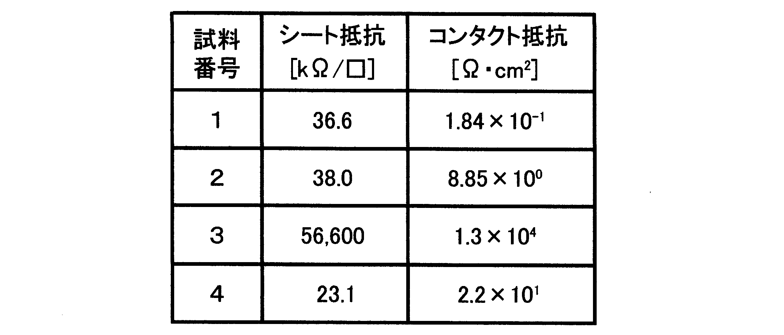
表1から分かるように、試料3はコンタクト抵抗が非常に大きい。これは、同じ表面濃度でも最上層のp型GaN層の厚さとして20nmでは不足しており、また50nmであれば十分であることを示している。これは、低いコンタクト抵抗を得るためには、最上層のp型GaN層の厚さがある程度必要であることを示している。一方、p+ 型GaNコンタクト層26の厚さが120nmの試料2では、却ってコンタクト抵抗値が大きくなった。試料4では、構造が異なるもののp型GaN層25の厚さが600nmとなってもコンタクト抵抗は低下していなかった。これは、単層のp型GaN層25であり、試料1、2の構造と異なっているためであると考えられる。
以上の結果より、p+ 型GaNコンタクト層26のMg濃度、すなわちアクセプタ濃度が5.0×1019cm-3程度のときは、p+ 型GaNコンタクト層26の厚さとして20nm以上必要であることが分かった。
[実験2]
実験1の結果を踏まえて、追加の実験2を行った。実験2では、表面のMg濃度のみを増加させた試料5を作製し、コンタクト抵抗を測定した。具体的には、試料5の構造としては、実験1においてコンタクト抵抗が最も小さかった試料1の構造において、厚さ50nmのp+ 型GaNコンタクト層26を上下2層に分け、上層/下層=3nm(2×1020cm-3)/47nm(5×1019cm-3)としたものである。その結果を表2に示す。

表2より、試料5によれば、最表面のp+ 型GaNコンタクト層26をさらに高濃度にすることがコンタクト抵抗の低減に有効であることが分かった。
実験1の結果を踏まえて、追加の実験2を行った。実験2では、表面のMg濃度のみを増加させた試料5を作製し、コンタクト抵抗を測定した。具体的には、試料5の構造としては、実験1においてコンタクト抵抗が最も小さかった試料1の構造において、厚さ50nmのp+ 型GaNコンタクト層26を上下2層に分け、上層/下層=3nm(2×1020cm-3)/47nm(5×1019cm-3)としたものである。その結果を表2に示す。
[実験3]
分極超接合領域の必要条件を求めるために実験3を行った。実験3では、ホール(Hall)測定により分極超接合領域の正孔濃度の測定を行った。
分極超接合領域の必要条件を求めるために実験3を行った。実験3では、ホール(Hall)測定により分極超接合領域の正孔濃度の測定を行った。
分極超接合素子は2次元電子ガス(2DEG)と2次元正孔ガス(2DHG)とが分極効果によりほぼ等量生じているときに最大の耐圧を示す。現実には、上部のGaN層がアンドープ層のみである場合、表面準位やアンドープ層がn型化すること等によってバンドエネルギーが影響を受け、2DHGは殆ど生じない。しかし、Mgアクセプタの添加により、表面準位を補償し、かつ表面近傍のバンドを持ち上げることによって2DHGがAlGaN/GaNの上部ヘテロ界面に生じるようになる。
理想的には、Mgアクセプタ由来の過剰な正孔は生じずに、2DEG濃度と2DHG濃度とは等しく、かつそれ以外の正孔は存在しない方がよい。従って、そのようなp型GaN層25の設計が必要となる。
実験1、2の、特に試料1、2はMgの添加総量が多く、Mgアクセプタ由来の正孔が過剰に存在している。そこで、図9に示す試料1を用いて、図14Aおよび図14B(図14Bは図14AのA-A’線に沿っての断面図)に示すホール素子を作製し、p型GaN層25の厚さと正孔濃度および移動度との関係を調べた。
図14Aおよび図14Bに示すように、図9に示す試料1のアンドープGaN層24、p型GaN層25およびp+ 型GaNコンタクト層26の四隅をエッチングにより円形にパターニングした後、四隅に露出したアンドープAlx Ga1-x N層23の表面にTi/Al/Au電極28を形成し、その内側の四隅のp+ 型GaNコンタクト層26上にNi/Au電極29を形成し、2次元正孔に対するホール測定と2次元電子に対するホール測定とを可能とした。
次に、四隅以外の部分をp+ 型GaNコンタクト層26の表面からそれぞれ0nm、70nmの深さまでエッチングし、正孔および電子に対してホール測定を行った。ここで、p+ 型GaNコンタクト層26の表面から70nmの深さまでエッチングした場合は、p+ 型GaNコンタクト層26に加えてその下のp型GaN層25の上層部も除去したことに対応する。エッチング量が0nmの試料を試料6、エッチング量が70nmの試料を試料7とする。
表3に試料6、7の室温における正孔(2DHG)および電子(2DEG)のシート抵抗値、シート濃度および移動度を示す。
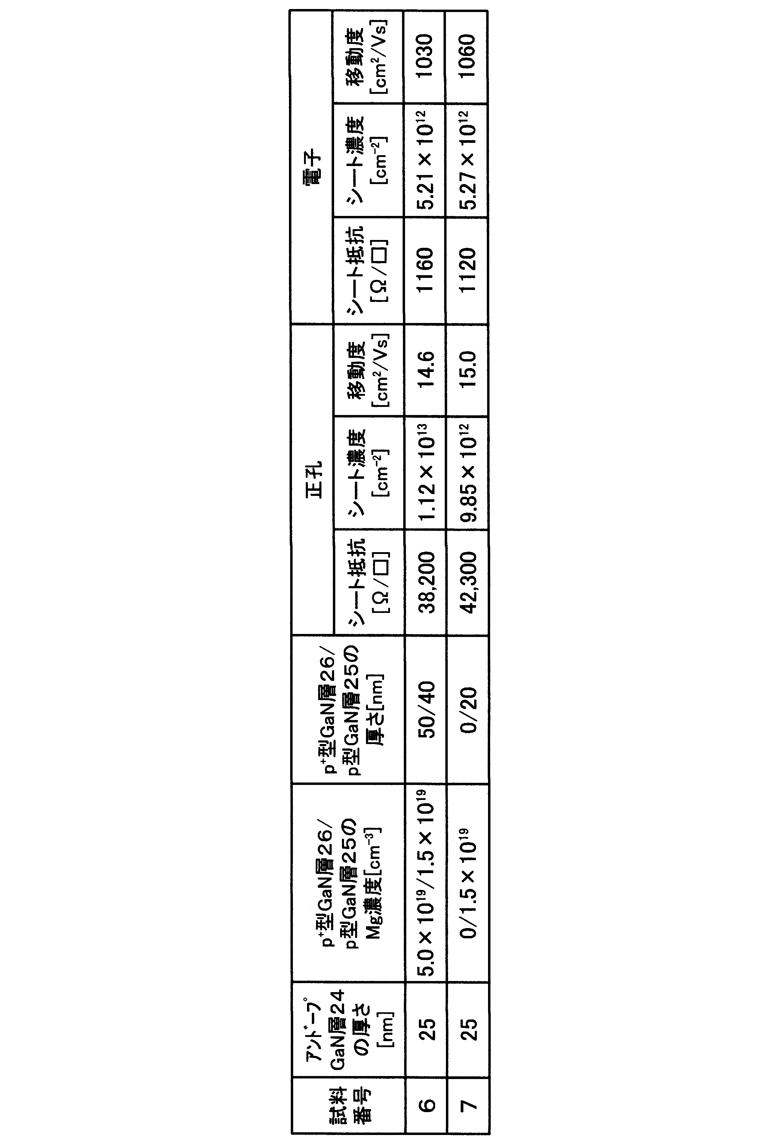
表3から分かるように、エッチング量が0nmの試料6の正孔濃度は1.12×1013cm-2であるのに対して、電子濃度は5.21×1012cm-2であった。エッチングを行い、p+ 型GaNコンタクト層26の厚さを小さくしてゆくと、正孔濃度はp+ 型GaNコンタクト層26を除去したときに若干減少し、その下のp型GaN層25を20nm除去したところ正孔濃度は減少しなかった。電子濃度の方は、エッチング量にかかわりなく約5.2×1012cm-2と一定値を示した。エッチング量が70nmの試料7において、正孔濃度は9.85×1012cm-2であった。
ここで、得られた正孔のシート濃度について検討を行う。
エッチング量が0nmの試料6について、p+ 型GaNコンタクト層26およびp型GaN層25の全体の合計のMgドープ量は、[Mg]=5.0×1019cm-3×50×10-7cm+1.5×1019cm-3×40×10-7cm=2.5×1014cm-2+6×1013cm-2=3.1×1014cm-2である。Mgアクセプタの室温の活性化率を1.0%とすると、3.1×1014×1.0×10-2=3.1×1012cm-2の正孔濃度となる。一方、実験値は表3に示すように1.12×1013cm-2であった。従って、正孔濃度は実験値の方が非常に大きく、この差{(11.2-3.1)×1012cm-2}=8.1×1012cm-2は分極によって生じた正孔である。
エッチング量が0nmの試料6について、p+ 型GaNコンタクト層26およびp型GaN層25の全体の合計のMgドープ量は、[Mg]=5.0×1019cm-3×50×10-7cm+1.5×1019cm-3×40×10-7cm=2.5×1014cm-2+6×1013cm-2=3.1×1014cm-2である。Mgアクセプタの室温の活性化率を1.0%とすると、3.1×1014×1.0×10-2=3.1×1012cm-2の正孔濃度となる。一方、実験値は表3に示すように1.12×1013cm-2であった。従って、正孔濃度は実験値の方が非常に大きく、この差{(11.2-3.1)×1012cm-2}=8.1×1012cm-2は分極によって生じた正孔である。
次に、エッチング量が70nmの試料7については、全体のMg量は、[Mg]=1.5×1019cm-3×20×10-7cm=3.0×1013cm-2であり、これによる正孔濃度は、Mgアクセプタの室温の活性化率を1.0%とすると、3.0×1011cm-2である。しかし、実験値は9.85×1012cm-2であった。実験値との差は(9.85-0.30)×1012=9.55×1012cm-2である。この結果より、この試料7の正孔は(9.55/9.85)×100=97.0%がMg由来でないもの、即ち分極によって生じたものであることが分かる。
一方、2次元電子濃度の変化は、p+ 型GaNコンタクト層26およびp型GaN層25のエッチングによっては殆ど変化せず、5.3×1012cm-2程度であった。
次に、正孔が分極によって発生した2次元正孔ガス(2DHG)であることを実証するため、低温でのホール測定を行った。Mgアクセプタの準位は価電子帯から160meV程度と深いので、200K以下の温度では正孔はMgアクセプタに落ち込み自由正孔は存在しなくなる。一方、分極由来の2DHGは低温にてもトラップされる準位がなくヘテロ界面に存在し続ける。従って、低温での正孔濃度は分極によって生成した2DHGのみによるものを示している。液体窒素温度(77K)での測定結果を表4に示す。

低温において、正孔濃度は、Mg由来の分だけ減少したと考える。低温における2DHG濃度はエッチング量が0nmの試料6で6.5×1012cm-2、エッチング量が70nmの試料7では6.0×1012cm-2であった。室温測定データから推測した2DHG濃度が、77K測定により実証された。正孔の移動度は、音響散乱の抑制により向上し、52~57cm2 /Vsが得られた。
[実験4]
次に、Mg量の絞り込み、言い換えると分極超接合素子として必要最小限のMg量の検討を行った。すなわち、Mg量はもっと減らすべきであると考えられるが、どこまで減らすことができるかについて検討を行った。そのために実験4を行った。
次に、Mg量の絞り込み、言い換えると分極超接合素子として必要最小限のMg量の検討を行った。すなわち、Mg量はもっと減らすべきであると考えられるが、どこまで減らすことができるかについて検討を行った。そのために実験4を行った。
以上の実験1~3では、正孔がどの程度のMgドープ量から消失するのかがまだ見えていなかった。そこで、実験4により、p型GaN層の限界実験を行った。限界実験とは、2DHG濃度が測定にかからなくなり、実質的に分極超接合素子としての効能がなくなる状態を検討・探索するものである。
分極超接合素子として有効であるのは、2DHGと2DEGとがアンドープAlx Ga1-x N層23を挟んで共存し、逆バイアス条件で両者が同時に空乏化することである。しかしながら、これは2DHG濃度と2DEG濃度とが等しいことを要求するものではない。2DHG濃度と2DEG濃度とがアンバランスであると、それに伴い分極超接合効果が減少し、例えば、その極限として、2DHG濃度が全く0cm-2の場合、通常のAlGaN/GaN HEMT構造と同一となり、その状態ではよく知られているように、逆バイアス時にアノード端にピーク電界が発生する。結局、2DHG濃度と2DEG濃度との量的バランスによってピーク電界の強度が依存することになる。実質的に、分極超接合効果が有効であるのは、すなわち、分極超接合であると言えるのは、2DHG濃度が2DEG濃度の1/10~1/5の場合であろう。1/10より小さいともはや、通常のHEMTと差異はなくなると推定される。ここでは、2DEG濃度の1/5を2DHG濃度のクライテリア(有効限界値)とおく。
そこで、実験的には、まず、通常のAlGaN/GaN HEMT構造を参照試料(レファレンス試料)として作製し、その2DEG濃度を確認し、次に、そのAlGaN層の構造条件においてアンドープGaN層およびp型GaN層を積層して分極超接合構造を作製し、その場合の2DEG濃度を確認すると同時に2DHG濃度を測定する。
具体的には、参照試料として、アンドープGaN層24およびp型GaN層25のない構造、すなわち、通常のAlGaN/GaN HEMT構造を基準用として作製した。サファイア基板上に、厚さ47nmでx=0.23のアンドープAlx Ga1-x N層23/アンドープGaN層22のHEMT構造で、アンドープGaN層22の厚さをそれぞれ、500nm、600nm、800nmと変化させた3種のHEMT試料(試料A-1、A-2、A-3)を作製し、それらの2DEG濃度を測定した。表5にその結果を示す。
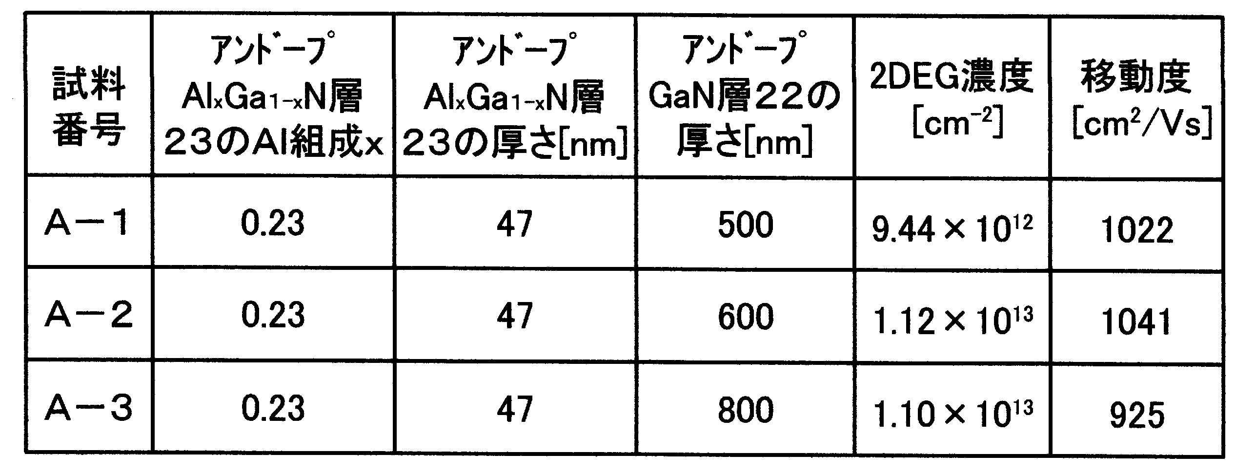
表5より、2DEG濃度は下地のアンドープGaN層22の厚さによって多少変化したが、アンドープGaN層22の厚さが600nm以上あれば、2DEG濃度は1.1×1013cm-2で一定となることが分かった。
さて、新たな試料として、図15に示す試料を作製した。図15に示すように、この試料は試料1と同様な構造を有するが、p型GaN層25の厚さは40nmとし、このp型GaN層25のMg濃度を5×1018cm-3、2×1018cm-3、5×1017cm-3、1×1017cm-3、0cm-3と変え、p+ 型GaNコンタクト層26を、厚さ47nmでMg濃度が5×1019cm-3の下部p+ 型GaNコンタクト層26aおよび厚さ3nmでMg濃度が2×1020cm-3の上部p+ 型GaNコンタクト層26bで構成した5種の試料8~12を作製した。また、試料10のp型GaN層25をエッチングにより、厚さ20nmまで薄化した試料13を作製した。試料8~13を用いて図16に示すようにホール測定試料を作製し、実験4と同じ方法により、ホール測定を行った。その結果を表6に示す。
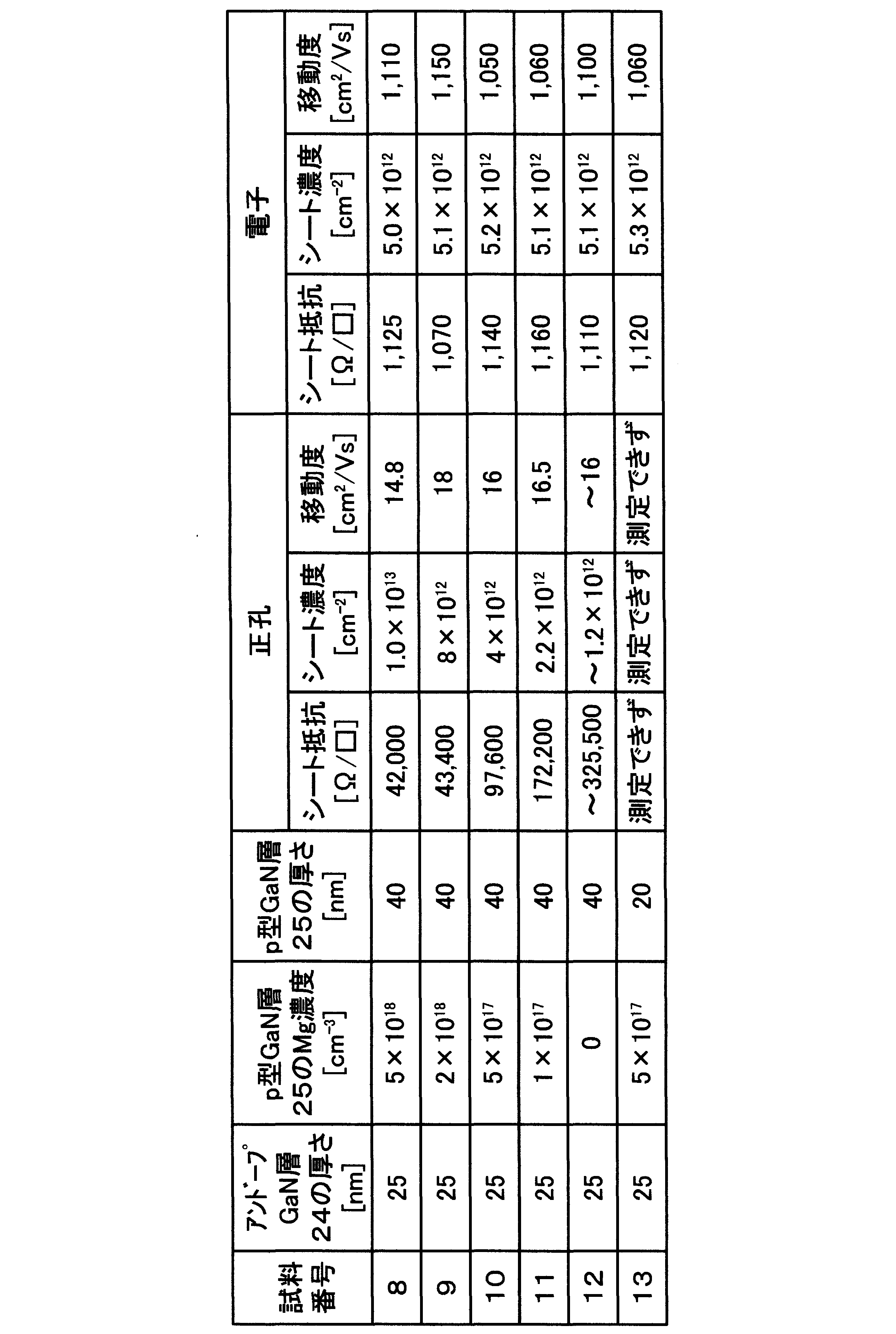
表6に示すように、シート電子濃度は概略5.0×1012cm-2~5.3×1012cm-2となり、標準HEMT構造(試料A-1、A-2、A-3)の約1/2に低下していた。アンドープGaN層24、p型GaN層25等が積層されることによって、バンドが上昇し、正孔が発生するとともに電子濃度が低下したものである。
次に、アンドープGaN層24の厚さを25nm、p型GaN層25の厚さを20nmとし、Mg濃度をそれぞれ、2×1018cm-3、5×1017cm-3および0cm-3とした3種の試料14~16を作製した。これらの試料14~16のホール測定の結果を表7に示す。
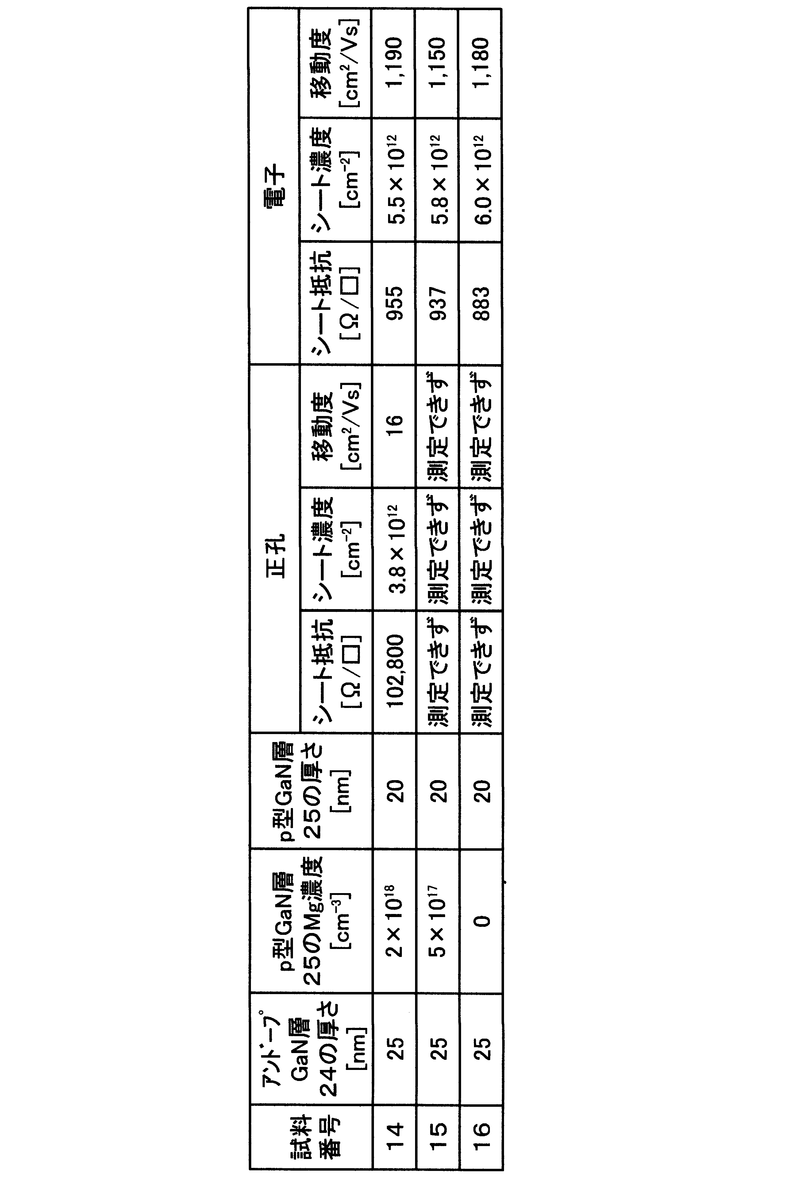
表7より、Mg濃度の少ない試料15および試料16では、非常に高抵抗で正孔濃度の測定は困難であった。電子濃度は(5.5~6.0)×1012cm-2とやや高かった。
次に、アンドープGaN層24の厚さを15nm、p型GaN層25の厚さを15nmとし、Mg濃度をそれぞれ、2×1018cm-3、5×1017cm-3および0cm-3とした3種の試料17~19を作製した。これらの試料17~19のホール測定の結果を表8に示す。

表8より、Mg濃度の少ない試料18および試料19では、非常に高抵抗で正孔濃度の測定は困難であった。電子濃度は(5.9~6.8)×1012cm-2であった。
[実験5]
次に、アンドープGaN層24の厚さが2DHG濃度に与える影響を確認するために、追加の実験5を行った。具体的には、アンドープGaN層24の厚さの下限を検討するために、アンドープGaN層24の厚さを80nmと厚くした試料20を作製した。図17に試料20の層の構造を示す。具体的には、C面サファイア基板21上に低温成長(530℃)でGaNバッファ層(図示せず)を厚さ30nm積層した後、成長温度を1100℃に上昇させ、厚さ800nmのアンドープGaN層22、厚さ47nmでx=0.23のアンドープAlx Ga1-x N層23、厚さ80nmのアンドープGaN層24、Mg濃度が5.0×1018cm-3で厚さ20nmのMgドープのp型GaN層25、Mg濃度が7.0×1019cm-3で厚さが37nmのp+ 型GaNコンタクト層26aおよびMg濃度が2.0×1020cm-3で厚さが3nmのMgドープp+ 型GaNコンタクト層26bを成長させることにより、試料20を作製した。図18に示すように、試料20のp+ 型GaNコンタクト層26aおよびp+ 型GaNコンタクト層26bの中央部を完全にエッチングし、さらにp型GaN層25の中央部をエッチングして厚さ10nmとすることにより試料21を作製した。図19に示すように、試料20のp型GaN層25、p+ 型GaNコンタクト層26aおよびp+ 型GaNコンタクト層26bの中央部を完全にエッチングし、さらにアンドープGaN層24の中央部をエッチングして厚さ75nmとすることにより試料22を作製した。図20に示すように、試料20のp型GaN層25、p+ 型GaNコンタクト層26aおよびp+ 型GaNコンタクト層26bの中央部を完全にエッチングし、さらにアンドープGaN層24をエッチングして厚さ30nmとすることにより試料23を作製した。
次に、アンドープGaN層24の厚さが2DHG濃度に与える影響を確認するために、追加の実験5を行った。具体的には、アンドープGaN層24の厚さの下限を検討するために、アンドープGaN層24の厚さを80nmと厚くした試料20を作製した。図17に試料20の層の構造を示す。具体的には、C面サファイア基板21上に低温成長(530℃)でGaNバッファ層(図示せず)を厚さ30nm積層した後、成長温度を1100℃に上昇させ、厚さ800nmのアンドープGaN層22、厚さ47nmでx=0.23のアンドープAlx Ga1-x N層23、厚さ80nmのアンドープGaN層24、Mg濃度が5.0×1018cm-3で厚さ20nmのMgドープのp型GaN層25、Mg濃度が7.0×1019cm-3で厚さが37nmのp+ 型GaNコンタクト層26aおよびMg濃度が2.0×1020cm-3で厚さが3nmのMgドープp+ 型GaNコンタクト層26bを成長させることにより、試料20を作製した。図18に示すように、試料20のp+ 型GaNコンタクト層26aおよびp+ 型GaNコンタクト層26bの中央部を完全にエッチングし、さらにp型GaN層25の中央部をエッチングして厚さ10nmとすることにより試料21を作製した。図19に示すように、試料20のp型GaN層25、p+ 型GaNコンタクト層26aおよびp+ 型GaNコンタクト層26bの中央部を完全にエッチングし、さらにアンドープGaN層24の中央部をエッチングして厚さ75nmとすることにより試料22を作製した。図20に示すように、試料20のp型GaN層25、p+ 型GaNコンタクト層26aおよびp+ 型GaNコンタクト層26bの中央部を完全にエッチングし、さらにアンドープGaN層24をエッチングして厚さ30nmとすることにより試料23を作製した。
試料20~23を用いてホール測定を行った結果を表9に示す。
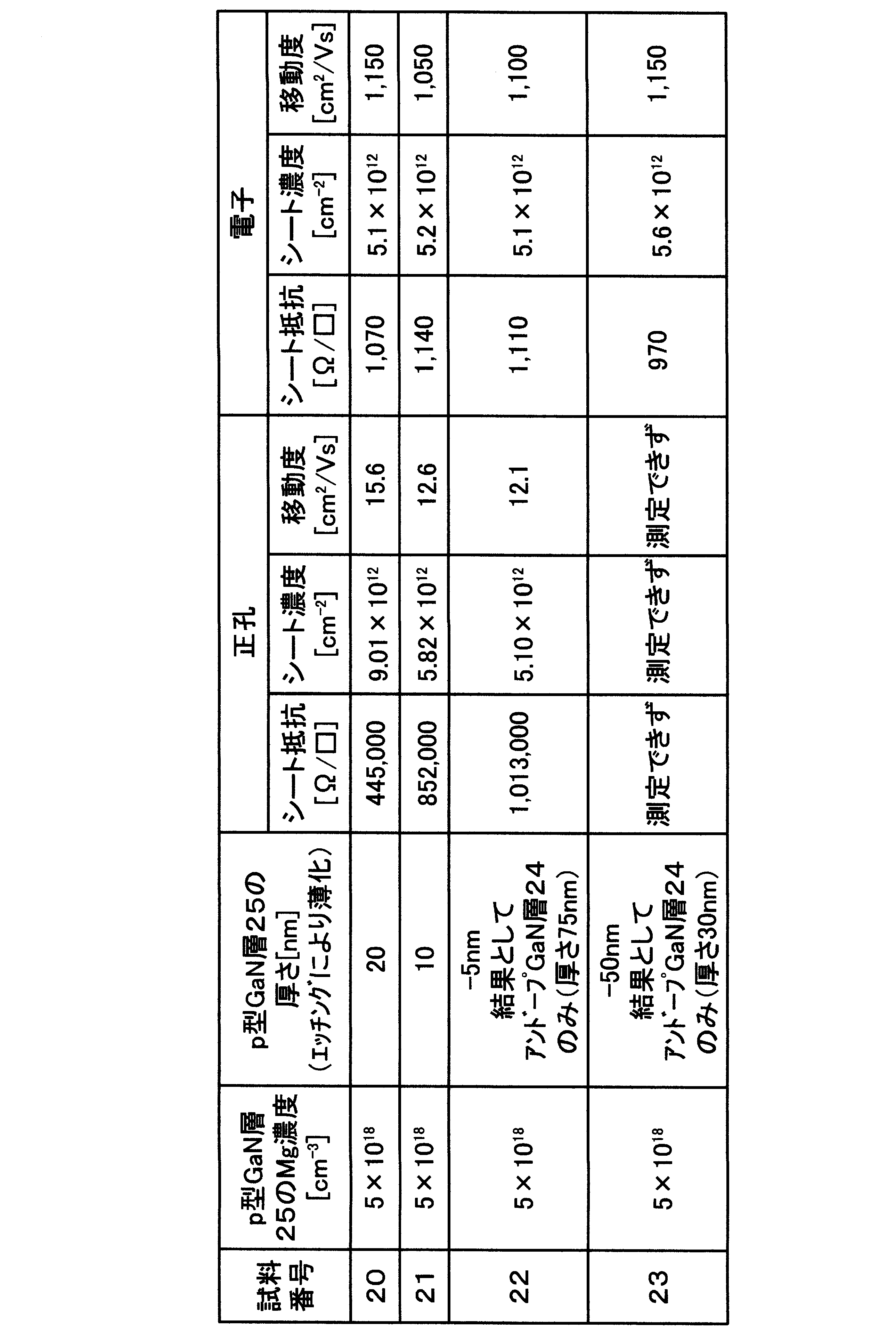
表9に示すように、エッチングなしの試料20の正孔濃度は9.01×1012cm-2であったのに対して、試料21および試料22の正孔濃度はそれぞれ5.82×1012cm-2および5.1×1012cm-2であった。試料23では、高抵抗で電流が流れず正孔の存在を確認できなかった。
以上の試料7~23の構造や2DHG濃度などを表10にまとめて示す。表10では、第1列目に試料番号を、第2~第4列目に、アンドープGaN層24の厚さ、p型GaN層25の厚さおよびp型GaN層25のMg濃度(1×1018cm-3を単位とする)を示した。また、第6列目に、測定された2DHG濃度を示した。第5列目は、実験値を整理するために導入した新しい指標である「換算厚さ(Reduced thickness)」という新しい概念に基づく値である。
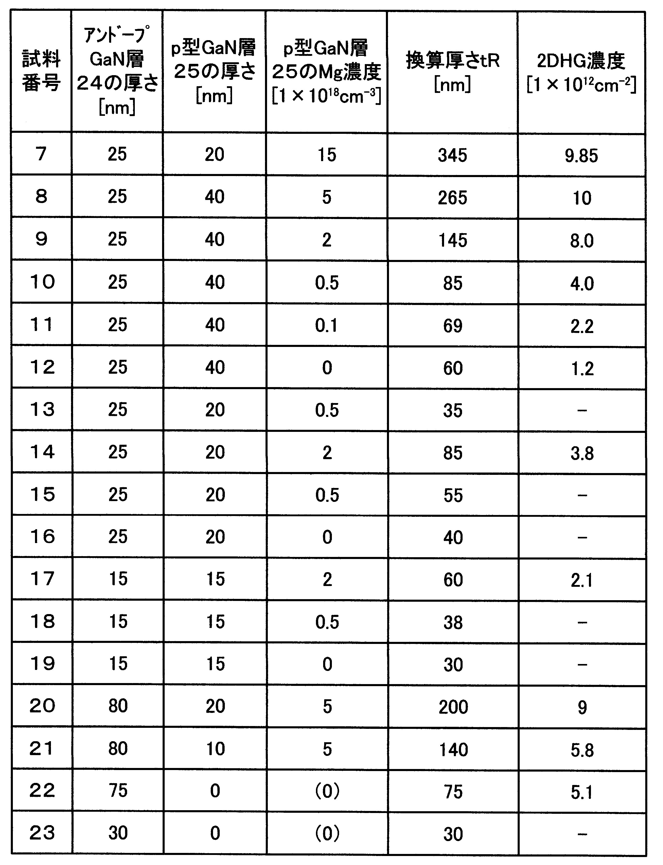
換算厚さについて説明する。換算厚さをtRと表す。換算厚さtRは次の式で表される量である。アンドープGaN層24の厚さをu[nm]で表し、p型GaN層25の厚さをv[nm]、Mg濃度をw[cm-3]で表したとき、換算厚さtRは、
tR=u+v(1+w×10-18 ) (1)
と定義される。この式の右辺の項の意味を説明する。p型GaN層25はフェルミ準位を基準にして、アンドープGaN層24よりもバンドが持ち上がっている。すなわち、表面側AlGaN/GaNヘテロ接合界面のバンドが持ち上がり2DHGを生成する効果は、p型GaN層25の方がアンドープGaN層24よりも大きい。そこで、p型GaN層25中のMgドーパントの効果を考察する。通常Mgドーパントの室温での活性化率は1%程度である。また、GaN層中には深い準位やn型不純物が1016cm-3から1017cm-3存在し、Mgのアクセプタとしての役割を妨げる。従って、1017cm-3台のMg濃度はp型としての役割はそれほど大きくない。従って、Mg濃度が1017cm-3よりも低い場合はむしろアンドープ層に近い。従って、p型GaN層25が本構造の2DHG濃度に与える寄与度を評価する場合、それの効果を取り入れる必要があり、それは1018cm-3を規格化の値とすることにより与えられることが上記の考察から、第1次近似として導き出される。従って、2DHG濃度は、式(1)で表される換算厚さtRに対して、1次の関係およびその後の飽和曲線になることが期待される。表10の第5列目は、式(1)で計算される換算厚さtRを示したものである。
tR=u+v(1+w×10-18 ) (1)
と定義される。この式の右辺の項の意味を説明する。p型GaN層25はフェルミ準位を基準にして、アンドープGaN層24よりもバンドが持ち上がっている。すなわち、表面側AlGaN/GaNヘテロ接合界面のバンドが持ち上がり2DHGを生成する効果は、p型GaN層25の方がアンドープGaN層24よりも大きい。そこで、p型GaN層25中のMgドーパントの効果を考察する。通常Mgドーパントの室温での活性化率は1%程度である。また、GaN層中には深い準位やn型不純物が1016cm-3から1017cm-3存在し、Mgのアクセプタとしての役割を妨げる。従って、1017cm-3台のMg濃度はp型としての役割はそれほど大きくない。従って、Mg濃度が1017cm-3よりも低い場合はむしろアンドープ層に近い。従って、p型GaN層25が本構造の2DHG濃度に与える寄与度を評価する場合、それの効果を取り入れる必要があり、それは1018cm-3を規格化の値とすることにより与えられることが上記の考察から、第1次近似として導き出される。従って、2DHG濃度は、式(1)で表される換算厚さtRに対して、1次の関係およびその後の飽和曲線になることが期待される。表10の第5列目は、式(1)で計算される換算厚さtRを示したものである。
次に、表10の第5列目の換算厚さtRをx軸に、第6列目の2DHG濃度をy軸に図示したものを図21に示す。また、図21のうち換算厚さtRが20~90nmの領域の拡大図を図22に示す。図21および図22中の数値は試料番号を示す。図21において、2DHG濃度は、換算厚さtRに対して概略比例し、換算厚さtRが大きくなると、2DHG濃度が1×1013cm-2付近で飽和する傾向にあることが分かった。2DHG濃度の小さい領域(図22)では、ホール測定の測定誤差が大きくなるので若干ばらついているが、2DHG濃度は、換算厚さtRに対して概略比例関係にあることが確認できた。換算厚さtRが50nm以下では正孔濃度は測定できなかった。ホール測定の誤差が大きくなる理由は、正孔の移動度が電子のそれの~1/100と非常に小さいので、測定されるホール(Hall)電圧が小さいこと、および、p型GaN層25へのオーミック電極のコンタクト抵抗値が本来的に高い(実験的には、n型GaN層へのオーミック電極のコンタクト抵抗値の105 倍)こと等による。
さて、通常HEMT構造の比較試料A-3では、2DEG濃度は概ね1.1×1013cm-2であった(表5参照。)。また、本分極超接合構造にした場合の2DEG濃度は、試料8から試料23までを通じて、概ね、(5.1~6.8)×1012cm-2であった。これは、アンドープAlx Ga1-x N層23の上の比較的厚いアンドープGaN層24およびp型GaN層25によるバンド持ち上がり効果により、アンドープAlx Ga1-x N層23とアンドープGaN層22とにより形成される下側のAlGaN/GaNヘテロ接合の2DEG濃度を減少させるからである。また、換算厚さtRが小さいほど、すなわち、バンドの持ち上がりが少ないほど2DEG濃度は小幅ながら増加していることも理解できることである。そうではあるが、興味深いことに、上部のアンドープGaN層24およびp型GaN層25の組合せ変化に対して、ほぼ一定の2DEG濃度(5.1~6.8)×1012cm-2になっていることの方に注目する。
すなわち、本分極超接合構造にした場合の2DEG濃度は、基準HEMTの2DEG濃度の約1/2となっている。このことは、基準HEMTの2DEG濃度が、対応するアンドープAlx Ga1-x N層23を持つ分極超接合構造の有効な2DHG濃度の下限(限界2DHG濃度)を規定することができることを意味する。すなわち、この基準HEMT構造の2DEG濃度を基準に用いることができる。
さて、分極超接合効果が顕著に得られるためには、有効2DHG濃度は2DEG濃度に対して1/10~1/5程度以上必要であることを既に説明したが、ここでは、1/5以上を条件とする。基準HEMTの2DEG濃度(1.1×1013cm-2)を基準にとると、分極超接合の有効下限2DHG濃度は、2DEG濃度の1/10=1.1×1012cm-2である。それを、図22の横線で示した。さて、図22を参照すると、2DHG濃度が1.1×1012cm-2に対する換算厚さの値はtR=55nmである。即ち、アンドープGaN層24の厚さをu[nm]、p型GaN層25の厚さをv[nm]、そのMg濃度をw[cm-3]とすると、分極超接合として有効な構造は式(1)のtRにおいて、
tR≧55[nm] (2)
である。
tR≧55[nm] (2)
である。
以上の換算厚さtRの有効範囲は、アンドープAlx Ga1-x N層23のAl組成xが0.23および厚さが47nmのときに得られたものである。それでは、それと異なるAl組成および厚さのときにはどうなるであろうか。
まず、基準となる2DEG濃度を得るために、アンドープAlx Ga1-x N層23のAl組成xおよび厚さを変化させた基準HEMTを作製した。表11にそれを示す。
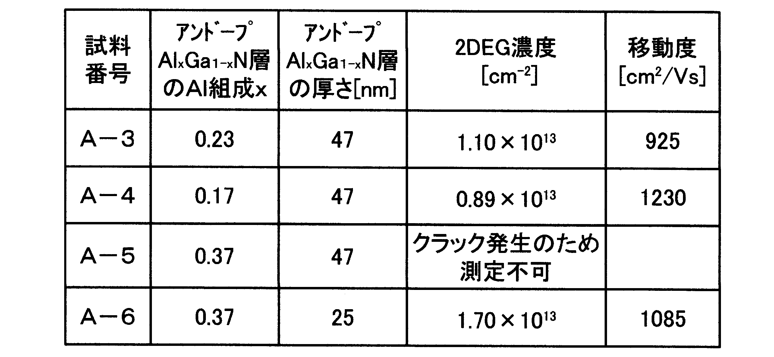
試料A-3は既出の試料である。試料A-4は、Al組成xが0.17で厚さが47nm、試料A-5は、Al組成xが0.37で厚さは47nm、試料A-6は、Al組成xが0.37で厚さが25nmである。実は、試料A-5は、結晶にクラックが発生し、膜が断裂していて測定が不可能であった。もともと、試料A-5は、アンドープAlx Ga1-x N層23の厚さが理論的な臨界膜厚を大きく超えているが、厚さを47nmに固定しようと敢えて作製したものである。従って、代替として、試料A-6は、アンドープAlx Ga1-x N層23の厚さを25nmと小さくした。2DEG濃度は、それぞれ、試料A-4では0.89×1013cm-2、試料A-6では1.7×1013cm-2であった。図23は、Alx Ga1-x N層のAl組成xとシートキャリア濃度(2DEG濃度)との関係を掲載している公知の文献(F.Calle et al. Journal of Materials Science:Materials in Electronics 14(2003)271-277)のp.272のFig.1を示すが、これに試料A-3、A-4、A-6のデータ(△、○、☆)を示す。この参考文献では、Alx Ga1-x N層のAl組成xを0.16から0.36まで、厚さを17nmから42nmまで変化させている。2DEG濃度はAl組成に対して比例的に増加し、厚さに対しては、厚さを増加すれば歪も増加するので増加傾向にあるが、顕著には増加していないことが見られる。試料A-3、A-4、A-6の2DEG濃度は文献値よりも相対的に大きくなっている。これは、本試料A-3、A-4、A-6の結晶品質が高く、格子緩和の程度が文献の試料より少なく、ヘテロ接合の格子歪が大きくて、分極効果が大きく出ているためであると考えられる。
次に、試料A-4のアンドープAlx Ga1-x N層23上に、厚さ80nmのアンドープGaN層24、厚さが40nmでMg濃度が1×1018cm-3のp型GaN層25、厚さが44nmでMg濃度が5×1019cm-3のp+ 型GaN層26aおよび厚さが3nmでMg濃度が2×1020cm-3のp+ 型GaN層26bを積層して試料24を作製した。この試料24のp型GaN層25をエッチングにより厚さ20nmにして試料25を作製した。この試料24のp型GaN層25をエッチングにより完全に除去した後、アンドープGaN層24を深さ5nmまでエッチングし、厚さを75nmにして試料26を作製した。また、この試料24のp型GaN層25をエッチングにより完全に除去した後、アンドープGaN層24を深さ30nmまでエッチングし、厚さを50nmとして試料27を作製した。これらの試料24~27のホール測定の結果を表12に示す。

試料27の正孔濃度は測定できなかった。2DEG濃度はアンドープGaN層24の厚さが小さくなるにつれて増加し、(3.8~4.1)×1012cm-2であった。この2DEG濃度は、試料A-4の2DEG濃度、8.9×1012cm-2の42%から46%であった。
次に、試料A-6の上に、試料24と同様なアンドープGaN層24、p型GaN層25、p+ 型GaN層26aおよびp+ 型GaN層26bを積層して分極超接合構造の試料28を作製した。同様に、エッチングにより、p型GaN層25の厚さを20nmとした試料29、アンドープGaN層24の厚さを75nmとした試料30、アンドープGaN層24の厚さを46nmとした試料31を作製した。これらの試料28~31のホール測定の結果を表13に示す。

これらの試料28~31はアンドープAlx Ga1-x N層23のAl組成xが0.35と高いので、すべての試料において2DHG濃度が測定できた。また、2DEG濃度は、(7.4~8.2)×1012cm-2であった。この2DEG濃度は基準HEMT構造の試料A-6の2DEG濃度(1.7×1013cm-2)の44%~48%であった。
次に、試料24~31に対して換算厚さtRを計算した。その結果を表14に示す。
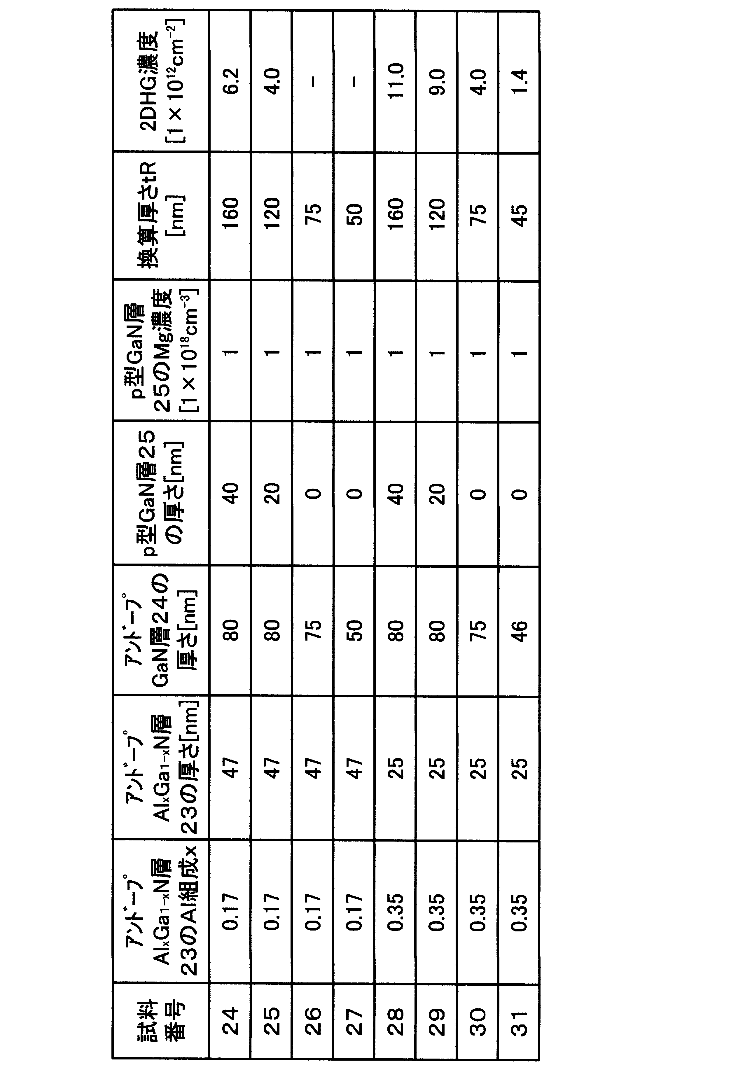
図24に、換算厚さtRを横軸に、縦軸に2DHG濃度をグラフとして図示した。図24内の数値は試料番号である。図24には、試料8~23のデータも併せて示した。ただし、それらの試料番号の表示は省略した。図24において、換算厚さtRと2DHG濃度との関係は、2DHG濃度が1×1013cm-2より少ない場合は概略直線関係となっていることが判明した。素子が動作する限界の換算厚さtRを推定するために、図24の換算厚さtRが0~150nmの部分を拡大して図25に示す。図25に、基準試料である試料A-3、A-4、A-6の2DEG濃度の1/10の値、すなわち、限界2DHG濃度を横線で示した。すなわち、限界2DHG濃度は、試料A-3では1.1×1012cm-2、試料A-4では0.89×1012cm-2、試料A-6では1.7×1012cm-2である。この限界2DHG濃度は,素子が分極超接合素子として動作するに必要な最低限の2DHG濃度である。それは、前に説明した通り、分極超接合素子として有効な2DHG濃度は2DEG濃度とのバランスが重要であり、その値は共存する2DEGの濃度の1/5から1/10であることを述べたが、ここで濃度の高い方向の(厳しい方の)1/5を採用している。
図25において、限界2DHG濃度に達する換算厚さtRは、アンドープAlx Ga1-x N層23のAl組成が0.17、厚さが47nmの試料24~27では70nm、Al組成が0.23、厚さが47nmの試料8~23では55nm、Al組成が0.35、厚さが25nmの試料28~31では50nmとなった。アンドープAlx Ga1-x N層23のAl組成xが0.23の素子のデータについては、図22より、限界厚さは55nmであった。Al組成xが0.35の試料のアンドープAlx Ga1-x N層の厚さは25nmであるが、図23に見られるように、この厚さの領域(17nmから42nm)では2DEG濃度の厚さ依存性は高々30%程度で、特に本件の実験の厚さ(25nm~47nm)の範囲では、上記3つの試料グループの限界厚さは、Al組成の違いとして理解することができる。
さて、アンドープAlx Ga1-x N層23のAl組成xに対して、限界2DHG濃度に対する換算厚さtRをプロットしたものが図26である。図26の3つのデータは各々のAl組成xに対する限界換算厚さである。図26に、これらの3点を通る曲線を示した。この曲線は、Al組成をx、限界厚さをy[nm]としたとき、下記の式(3)で与えられるものである。
y=a/(x-b)+c (3)
ただし、a=0.864
b=0.134
c=46.0
この式(3)は、アンドープAlx Ga1-x N層23のAl組成xが異なる構造に対して限界厚さを与えるために採用した経験式である。
y=a/(x-b)+c (3)
ただし、a=0.864
b=0.134
c=46.0
この式(3)は、アンドープAlx Ga1-x N層23のAl組成xが異なる構造に対して限界厚さを与えるために採用した経験式である。
分極超接合構造のアンドープAlx Ga1-x N層23のAl組成xが0.17から0.35で、厚さが概ね25nmから47nmにある場合、換算厚さtRが式(3)で示す限界厚さよりも大きいことが必要である。すなわち、Al組成が0.17から0.35、厚さが25nmから47nmの範囲において、適用換算厚さtRは、
tR≧0.864/(x-0.134)+46.0[nm] (4)
である。
tR≧0.864/(x-0.134)+46.0[nm] (4)
である。
高性能の分極超接合素子を実現させるための設計においては、以上のような低いまたはゼロ(0)のMg量の分極超接合領域においてもp電極の低接触抵抗を実現させることが必要であり、それには、分極超接合領域とp電極コンタクト領域とを構造的に分離し、p電極コンタクト領域に、p型GaN層25よりも高濃度のアクセプタ濃度(Mg濃度)を有するp+ 型GaNコンタクト層を設け、このp+ 型GaNコンタクト層にp電極をコンタクトさせる。
図14Aおよび図14Bや図16に示すホール測定試料においては、最上層のp+ 型GaNコンタクト層26の中央部をエッチングすることによって、分極超接合領域とp電極コンタクト領域とを作製しているが、例えば、図27または図28Aおよび図28Bに示すような方法を用いて分極超接合領域とp電極コンタクト領域とを作製してもよい。すなわち、図27に示すように、p型GaN層25まで成長させた後、その上にSiO2 膜などの誘電体膜からなる成長マスク30を形成し、この成長マスク30の一部をエッチングにより除去して開口を形成し、この開口に露出したp型GaN層25上にp+ 型GaNコンタクト層26を選択成長させる。あるいは、図28Aに示すように、p型GaN層25まで成長させた後、その上にSiO2 膜などの誘電体膜からなる成長マスク30を形成し、この成長マスク30の一部をエッチングにより除去して開口を形成し、この成長マスク30を用いてアンドープAlx Ga1-x N層23の途中の深さまでエッチングして溝31を形成する。そして、図28Bに示すように、成長マスク30を用いてこの溝31の内部にp+ 型GaNコンタクト層26を選択成長させて埋め込む。
次に、この半導体素子を電界効果トランジスタおよびダイオードに適用した具体的な構造例について説明する。
[第1の構造例]
図29は4端子構造の電界効果トランジスタを示す。図29に示すように、アンドープGaN層41、厚さが25nm以上47nm以下のアンドープAlx Ga1-x N層42(0.17≦x≦0.35)、アンドープGaN層43およびp型GaN層44が順次積層されている。アンドープAlx Ga1-x N層42上のアンドープGaN層43およびp型GaN層44はメサ型にパターニングされ、p型GaN層44上にp+ 型GaNコンタクト層45がメサ型で設けられている。アンドープGaN層43およびp型GaN層44を挟んでアンドープAlx Ga1-x N層42上にソース電極46およびドレイン電極47が設けられている。ソース電極46およびドレイン電極47は、例えばTi/Al二層膜により構成され、アンドープAlx Ga1-x N層42に対してオーミック接触している。ソース電極46とアンドープGaN層43およびp型GaN層44との間の部分のアンドープAlx Ga1-x N層42上にゲート電極48が設けられ、p+ 型GaNコンタクト層45上にp電極49が設けられている。ゲート電極48は、例えばNi/Au二層膜により構成され、アンドープAlx Ga1-x N層42に対してショットキー接触している。p電極49は、例えばNi/Au二層膜により構成され、p+ 型GaNコンタクト層45に対してオーミック接触している。この電界効果トランジスタは、p電極49とソース電極46とを接続する方式(これは金属フィールドプレート(FP)方式のソースフィールドプレートに相当する)およびp電極49とゲート電極48とを接続する方式(p電極49をベース電極と考えるとこれはベースフィールドプレートに相当する)の両方式に対応できる構造である。なお、図29においては、ソース電極46とゲート電極48との間、ゲート電極48とアンドープGaN層43との間およびアンドープGaN層43とドレイン電極47との間の部分のアンドープAlx Ga1-x N層42が露出しているが、必要に応じてアンドープAlx Ga1-x N層42の表面をアンドープGaN層で覆うことにより露出しないようにすることができる。
図29は4端子構造の電界効果トランジスタを示す。図29に示すように、アンドープGaN層41、厚さが25nm以上47nm以下のアンドープAlx Ga1-x N層42(0.17≦x≦0.35)、アンドープGaN層43およびp型GaN層44が順次積層されている。アンドープAlx Ga1-x N層42上のアンドープGaN層43およびp型GaN層44はメサ型にパターニングされ、p型GaN層44上にp+ 型GaNコンタクト層45がメサ型で設けられている。アンドープGaN層43およびp型GaN層44を挟んでアンドープAlx Ga1-x N層42上にソース電極46およびドレイン電極47が設けられている。ソース電極46およびドレイン電極47は、例えばTi/Al二層膜により構成され、アンドープAlx Ga1-x N層42に対してオーミック接触している。ソース電極46とアンドープGaN層43およびp型GaN層44との間の部分のアンドープAlx Ga1-x N層42上にゲート電極48が設けられ、p+ 型GaNコンタクト層45上にp電極49が設けられている。ゲート電極48は、例えばNi/Au二層膜により構成され、アンドープAlx Ga1-x N層42に対してショットキー接触している。p電極49は、例えばNi/Au二層膜により構成され、p+ 型GaNコンタクト層45に対してオーミック接触している。この電界効果トランジスタは、p電極49とソース電極46とを接続する方式(これは金属フィールドプレート(FP)方式のソースフィールドプレートに相当する)およびp電極49とゲート電極48とを接続する方式(p電極49をベース電極と考えるとこれはベースフィールドプレートに相当する)の両方式に対応できる構造である。なお、図29においては、ソース電極46とゲート電極48との間、ゲート電極48とアンドープGaN層43との間およびアンドープGaN層43とドレイン電極47との間の部分のアンドープAlx Ga1-x N層42が露出しているが、必要に応じてアンドープAlx Ga1-x N層42の表面をアンドープGaN層で覆うことにより露出しないようにすることができる。
[第2の構造例]
図30は3端子構造の電界効果トランジスタを示す。図30に示すように、アンドープGaN層41、アンドープAlx Ga1-x N層42、アンドープGaN層43およびp型GaN層44が順次積層されている。アンドープAlx Ga1-x N層42上のアンドープGaN層43およびp型GaN層44はメサ型にパターニングされ、p型GaN層44上にp+ 型GaNコンタクト層45がメサ型で設けられている。アンドープGaN層43およびp型GaN層44を挟んでアンドープAlx Ga1-x N層42上にソース電極46およびドレイン電極47が設けられている。ソース電極46とアンドープGaN層43およびp型GaN層44との間の部分のアンドープAlx Ga1-x N層42上にp電極49を兼用するゲート電極48が、アンドープGaN層43およびp型GaN層44の端面からp+ 型GaNコンタクト層45上に延在して設けられている。ゲート電極48は、例えばNi/Au二層膜からなり、p+ 型GaNコンタクト層45に対してオーミック接触している。この電界効果トランジスタは、ゲート電極48とp電極49とを一体化した3端子構造を有し、図25に示す電界効果トランジスタにおいてゲート電極48とp電極49とを一体化したものと等価である。
図30は3端子構造の電界効果トランジスタを示す。図30に示すように、アンドープGaN層41、アンドープAlx Ga1-x N層42、アンドープGaN層43およびp型GaN層44が順次積層されている。アンドープAlx Ga1-x N層42上のアンドープGaN層43およびp型GaN層44はメサ型にパターニングされ、p型GaN層44上にp+ 型GaNコンタクト層45がメサ型で設けられている。アンドープGaN層43およびp型GaN層44を挟んでアンドープAlx Ga1-x N層42上にソース電極46およびドレイン電極47が設けられている。ソース電極46とアンドープGaN層43およびp型GaN層44との間の部分のアンドープAlx Ga1-x N層42上にp電極49を兼用するゲート電極48が、アンドープGaN層43およびp型GaN層44の端面からp+ 型GaNコンタクト層45上に延在して設けられている。ゲート電極48は、例えばNi/Au二層膜からなり、p+ 型GaNコンタクト層45に対してオーミック接触している。この電界効果トランジスタは、ゲート電極48とp電極49とを一体化した3端子構造を有し、図25に示す電界効果トランジスタにおいてゲート電極48とp電極49とを一体化したものと等価である。
[第3の構造例]
図31はノーマリーオフ型の3端子構造の電界効果トランジスタを示す。図31に示すように、アンドープGaN層41、アンドープAlx Ga1-x N層42、アンドープGaN層43およびp型GaN層44が順次積層されている。アンドープAlx Ga1-x N層42上のアンドープGaN層43およびp型GaN層44はメサ型にパターニングされ、p型GaN層44上にp+ 型GaNコンタクト層45がメサ型で設けられている。アンドープGaN層43およびp型GaN層44を挟んでアンドープAlx Ga1-x N層42上にソース電極46およびドレイン電極47が設けられている。ソース電極46とアンドープGaN層43およびp型GaN層44との間の部分のアンドープAlx Ga1-x N層42に溝がアンドープGaN層43およびp型GaN層44の端面に連なって設けられ、p電極49を兼用するゲート電極48が、この溝の内部に埋め込まれ、さらにアンドープGaN層43およびp型GaN層44の端面からp+ 型GaNコンタクト層45上に延在している。この電界効果トランジスタの閾値電圧の制御は、アンドープAlx Ga1-x N層42に設けられた溝の部分のアンドープAlx Ga1-x N層42の厚さ、あるいは溝形成時のエッチング残し量によって行う。
図31はノーマリーオフ型の3端子構造の電界効果トランジスタを示す。図31に示すように、アンドープGaN層41、アンドープAlx Ga1-x N層42、アンドープGaN層43およびp型GaN層44が順次積層されている。アンドープAlx Ga1-x N層42上のアンドープGaN層43およびp型GaN層44はメサ型にパターニングされ、p型GaN層44上にp+ 型GaNコンタクト層45がメサ型で設けられている。アンドープGaN層43およびp型GaN層44を挟んでアンドープAlx Ga1-x N層42上にソース電極46およびドレイン電極47が設けられている。ソース電極46とアンドープGaN層43およびp型GaN層44との間の部分のアンドープAlx Ga1-x N層42に溝がアンドープGaN層43およびp型GaN層44の端面に連なって設けられ、p電極49を兼用するゲート電極48が、この溝の内部に埋め込まれ、さらにアンドープGaN層43およびp型GaN層44の端面からp+ 型GaNコンタクト層45上に延在している。この電界効果トランジスタの閾値電圧の制御は、アンドープAlx Ga1-x N層42に設けられた溝の部分のアンドープAlx Ga1-x N層42の厚さ、あるいは溝形成時のエッチング残し量によって行う。
[第4の構造例]
図32は3端子構造の電界効果トランジスタを示す。図32に示すように、アンドープGaN層41、アンドープAlx Ga1-x N層42、アンドープGaN層43およびp型GaN層44が順次積層されている。アンドープAlx Ga1-x N層42上のアンドープGaN層43およびp型GaN層44はメサ型にパターニングされ、p型GaN層44上にp+ 型GaNコンタクト層45がメサ型で設けられている。アンドープGaN層43およびp型GaN層44を挟んでアンドープAlx Ga1-x N層42上にソース電極46およびドレイン電極47が設けられている。p+ 型GaNコンタクト層45上にゲート電極48を兼用するp電極49が設けられている。この電界効果トランジスタの動作は、閾値電圧が深く(負側にシフト)なるほかは図31に示す電界効果トランジスタと同様である。
図32は3端子構造の電界効果トランジスタを示す。図32に示すように、アンドープGaN層41、アンドープAlx Ga1-x N層42、アンドープGaN層43およびp型GaN層44が順次積層されている。アンドープAlx Ga1-x N層42上のアンドープGaN層43およびp型GaN層44はメサ型にパターニングされ、p型GaN層44上にp+ 型GaNコンタクト層45がメサ型で設けられている。アンドープGaN層43およびp型GaN層44を挟んでアンドープAlx Ga1-x N層42上にソース電極46およびドレイン電極47が設けられている。p+ 型GaNコンタクト層45上にゲート電極48を兼用するp電極49が設けられている。この電界効果トランジスタの動作は、閾値電圧が深く(負側にシフト)なるほかは図31に示す電界効果トランジスタと同様である。
[第5の構造例]
図33はノーマリーオフ型の3端子構造の電界効果トランジスタを示す。図33に示すように、アンドープGaN層41、アンドープAlx Ga1-x N層42、アンドープGaN層43およびp型GaN層44が順次積層されている。アンドープAlx Ga1-x N層42上のアンドープGaN層43およびp型GaN層44はメサ型にパターニングされている。アンドープAlx Ga1-x N層42に、アンドープGaN層43およびp型GaN層44の端面に連なって溝が設けられ、この溝の内部にp+ 型GaNコンタクト層45が埋め込まれ、このp+ 型GaNコンタクト層45と2次元正孔ガス(図示せず)とが接合している。p+ 型GaNコンタクト層45は選択再成長により成長させることができる。アンドープGaN層43およびp型GaN層44を挟んでアンドープAlx Ga1-x N層42上にソース電極46およびドレイン電極47が設けられている。p+ 型GaNコンタクト層45上にゲート電極48を兼用するp電極49が設けられている。図31に示す電界効果トランジスタにおいては、ゲート電極48はショットキー接合型であるが、この電界効果トランジスタにおいては、ゲート電極48はp/n接合型である。このようにこの電界効果トランジスタのゲート電極48はp/n接合型であるが、p/n接合の拡散電位が3.4Vであり、ショットキー接合の拡散電位~1.4Vよりも+2V高く、ゲート閾値電圧を大きく取ることができる。p+ 型GaNコンタクト層45の下方の部分のアンドープAlx Ga1-x N層42を完全に除去し、アンドープGaN層41にp+ 型GaNコンタクト層45を接触させることも、閾値電圧の向上の観点から良い構造である。
図33はノーマリーオフ型の3端子構造の電界効果トランジスタを示す。図33に示すように、アンドープGaN層41、アンドープAlx Ga1-x N層42、アンドープGaN層43およびp型GaN層44が順次積層されている。アンドープAlx Ga1-x N層42上のアンドープGaN層43およびp型GaN層44はメサ型にパターニングされている。アンドープAlx Ga1-x N層42に、アンドープGaN層43およびp型GaN層44の端面に連なって溝が設けられ、この溝の内部にp+ 型GaNコンタクト層45が埋め込まれ、このp+ 型GaNコンタクト層45と2次元正孔ガス(図示せず)とが接合している。p+ 型GaNコンタクト層45は選択再成長により成長させることができる。アンドープGaN層43およびp型GaN層44を挟んでアンドープAlx Ga1-x N層42上にソース電極46およびドレイン電極47が設けられている。p+ 型GaNコンタクト層45上にゲート電極48を兼用するp電極49が設けられている。図31に示す電界効果トランジスタにおいては、ゲート電極48はショットキー接合型であるが、この電界効果トランジスタにおいては、ゲート電極48はp/n接合型である。このようにこの電界効果トランジスタのゲート電極48はp/n接合型であるが、p/n接合の拡散電位が3.4Vであり、ショットキー接合の拡散電位~1.4Vよりも+2V高く、ゲート閾値電圧を大きく取ることができる。p+ 型GaNコンタクト層45の下方の部分のアンドープAlx Ga1-x N層42を完全に除去し、アンドープGaN層41にp+ 型GaNコンタクト層45を接触させることも、閾値電圧の向上の観点から良い構造である。
[第6の構造例]
図34は3端子構造のダイオードを示す。図34に示すように、アンドープGaN層51、アンドープAlx Ga1-x N層52、アンドープGaN層53およびp型GaN層54が順次積層されている。アンドープAlx Ga1-x N層52上のアンドープGaN層53およびp型GaN層54はメサ型にパターニングされ、p型GaN層54上にp+ 型GaNコンタクト層55がメサ型で設けられている。アンドープGaN層53およびp型GaN層54を挟んでアノード電極56およびカソード電極57が設けられている。アノード電極56は、アンドープGaN層51に達する深さに設けられた溝58の内部に埋め込まれ、アンドープGaN層51とアンドープAlx Ga1-x N層52との間のヘテロ界面の近傍の部分におけるアンドープGaN層51に形成された2DEG(図示せず)と直接接触している。アノード電極56は、例えば、n型GaN系半導体に対しショットキー接触するNi/Au二層膜等で形成される。ソース電極57はアンドープAlx Ga1-x N層52上に設けられている。p+ 型GaNコンタクト層55上にp電極59が設けられている。アノード電極56とp電極59とは互いに電気的に接続されている。このダイオードは、図25に示す電界効果トランジスタのゲート電極48をその下のアンドープAlx Ga1-x N層52をエッチングしてアンドープGaN層51に接触させることによりショットキー接合を形成したものに相当する。必要に応じて、アノード電極56とp電極59とを一体に形成してもよい。
図34は3端子構造のダイオードを示す。図34に示すように、アンドープGaN層51、アンドープAlx Ga1-x N層52、アンドープGaN層53およびp型GaN層54が順次積層されている。アンドープAlx Ga1-x N層52上のアンドープGaN層53およびp型GaN層54はメサ型にパターニングされ、p型GaN層54上にp+ 型GaNコンタクト層55がメサ型で設けられている。アンドープGaN層53およびp型GaN層54を挟んでアノード電極56およびカソード電極57が設けられている。アノード電極56は、アンドープGaN層51に達する深さに設けられた溝58の内部に埋め込まれ、アンドープGaN層51とアンドープAlx Ga1-x N層52との間のヘテロ界面の近傍の部分におけるアンドープGaN層51に形成された2DEG(図示せず)と直接接触している。アノード電極56は、例えば、n型GaN系半導体に対しショットキー接触するNi/Au二層膜等で形成される。ソース電極57はアンドープAlx Ga1-x N層52上に設けられている。p+ 型GaNコンタクト層55上にp電極59が設けられている。アノード電極56とp電極59とは互いに電気的に接続されている。このダイオードは、図25に示す電界効果トランジスタのゲート電極48をその下のアンドープAlx Ga1-x N層52をエッチングしてアンドープGaN層51に接触させることによりショットキー接合を形成したものに相当する。必要に応じて、アノード電極56とp電極59とを一体に形成してもよい。
[第7の構造例]
図35は2端子構造のダイオードを示す。図35に示すように、アンドープGaN層51、アンドープAlx Ga1-x N層52、アンドープGaN層53およびp型GaN層54が順次積層されている。アンドープAlx Ga1-x N層52上のアンドープGaN層53およびp型GaN層54はメサ型にパターニングされている。アンドープAlx Ga1-x N層52に、アンドープGaN層53およびp型GaN層54の端面に連なって溝が設けられ、この溝の内部にp+ 型GaNコンタクト層55が埋め込まれ、このp+ 型GaNコンタクト層55と2次元正孔ガス(図示せず)とが接合している。アンドープGaN層53およびp型GaN層54を挟んでアノード電極56およびカソード電極57が設けられている。p+ 型GaNコンタクト層55に連なってアンドープGaN層51に達する深さの別の溝58が設けられている。アノード電極56は、この別の溝58の内部に埋め込まれ、さらにp+ 型GaNコンタクト層55上に延在している。アノード電極56は例えばNi/Au二層膜により形成される。ソース電極57はアンドープAlx Ga1-x N層52上に設けられている。
図35は2端子構造のダイオードを示す。図35に示すように、アンドープGaN層51、アンドープAlx Ga1-x N層52、アンドープGaN層53およびp型GaN層54が順次積層されている。アンドープAlx Ga1-x N層52上のアンドープGaN層53およびp型GaN層54はメサ型にパターニングされている。アンドープAlx Ga1-x N層52に、アンドープGaN層53およびp型GaN層54の端面に連なって溝が設けられ、この溝の内部にp+ 型GaNコンタクト層55が埋め込まれ、このp+ 型GaNコンタクト層55と2次元正孔ガス(図示せず)とが接合している。アンドープGaN層53およびp型GaN層54を挟んでアノード電極56およびカソード電極57が設けられている。p+ 型GaNコンタクト層55に連なってアンドープGaN層51に達する深さの別の溝58が設けられている。アノード電極56は、この別の溝58の内部に埋め込まれ、さらにp+ 型GaNコンタクト層55上に延在している。アノード電極56は例えばNi/Au二層膜により形成される。ソース電極57はアンドープAlx Ga1-x N層52上に設けられている。
[第8の構造例]
図36は2端子構造のダイオードを示す。図36に示すように、アンドープGaN層51、アンドープAlx Ga1-x N層52、アンドープGaN層53およびp型GaN層54が順次積層されている。アンドープAlx Ga1-x N層52上のアンドープGaN層53およびp型GaN層54はメサ型にパターニングされ、p型GaN層54上にp+ 型GaNコンタクト層55がメサ型で設けられている。アノード電極56とアンドープGaN層53およびp型GaN層54との間の部分のアンドープAlx Ga1-x N層52に溝60がアンドープGaN層53およびp型GaN層54の端面に連なって設けられている。この溝60の内部にp電極59が埋め込まれ、さらにアンドープGaN層53およびp型GaN層54の端面からp+ 型GaNコンタクト層55上に延在し、アノード電極56と一体になって互いに電気的に接続されている。このダイオードは、図32に示す、ゲート閾値電圧が0V以上のノーマリーオフ型(エンハンスメントモード)電界効果トランジスタのソース電極46とゲート電極48とを一体化させた構造を有する。カソード電極57に対してアノード電極56に正の電圧を印加するとショットキー接合がオンとなり、オーミック電極であるアノード電極56とカソード電極57との間に順電流が流れる。アノード電極56に負電圧を印加するとショットキー接合がオフとなり、隣に接しているアノード電極56とカソード電極57との間に電流は流れない。
図36は2端子構造のダイオードを示す。図36に示すように、アンドープGaN層51、アンドープAlx Ga1-x N層52、アンドープGaN層53およびp型GaN層54が順次積層されている。アンドープAlx Ga1-x N層52上のアンドープGaN層53およびp型GaN層54はメサ型にパターニングされ、p型GaN層54上にp+ 型GaNコンタクト層55がメサ型で設けられている。アノード電極56とアンドープGaN層53およびp型GaN層54との間の部分のアンドープAlx Ga1-x N層52に溝60がアンドープGaN層53およびp型GaN層54の端面に連なって設けられている。この溝60の内部にp電極59が埋め込まれ、さらにアンドープGaN層53およびp型GaN層54の端面からp+ 型GaNコンタクト層55上に延在し、アノード電極56と一体になって互いに電気的に接続されている。このダイオードは、図32に示す、ゲート閾値電圧が0V以上のノーマリーオフ型(エンハンスメントモード)電界効果トランジスタのソース電極46とゲート電極48とを一体化させた構造を有する。カソード電極57に対してアノード電極56に正の電圧を印加するとショットキー接合がオンとなり、オーミック電極であるアノード電極56とカソード電極57との間に順電流が流れる。アノード電極56に負電圧を印加するとショットキー接合がオフとなり、隣に接しているアノード電極56とカソード電極57との間に電流は流れない。
次に、図37に示すような分極超接合構造を適用した電界効果トランジスタを作製し、動作実験を行った結果について説明する。この動作実験により、p電極のコンタクト抵抗がトランジスタのスイッチング特性に与える影響を評価することができる。
図37に示すように、この電界効果トランジスタにおいては、アンドープGaN層61、アンドープAlx Ga1-x N層62、アンドープGaN層63およびp型GaN層64が順次積層されている。アンドープAlx Ga1-x N層62上のアンドープGaN層63およびp型GaN層64はメサ型にパターニングされている。アンドープGaN層63およびp型GaN層64を挟んでアンドープAlx Ga1-x N層62上にソース電極65およびドレイン電極66が設けられている。p型GaN層64上には、p電極を兼用するゲート電極67が設けられている。図37には、トランジスタがオンの状態の電子および正孔の状態を示す。符号68は2DHG、69は2DEGを示す。図38に、トランジスタがオフの状態の電子および正孔の状態を示す。図38では、ゲート電極67に負電圧が印加され、ゲート電極67を通じて正孔(2DHG68)が引き抜かれ、その直下の電子チャネル(2DEG69)が空乏化されている。このように、トランジスタのオン・オフ動作において、正孔(2DHG68)の注入/引抜きが行われる。もし、正孔(2DHG68)の移動に障害があれば、動特性に影響を及ぼす。
正孔(2DHG68)の移動に影響を及ぼす要因としては、正孔の移動度がある。正孔の移動度は表3に示したように実験的には15~30[cm2 /Vs]程度である。この値は電子の移動度の1/500~1/1000であり、正孔の移動速度が本トランジスタの速度を支配すると考えられる。とすると、スイッチング速度は通常のHFETの1/1000以下と推定される。従って、分極超接合領域の長さにも依るが、遮断周波数は数MHz~数10MHz程度と推定される。しかし、Si-IGBT(Insulated Gate Bipolar Transistor)のスイッチング周波数は高々数10kHzであり、また、Si-パワーMOSFETのそれは数MHzである。超接合を用いたこの電界効果トランジスタは高耐圧パワー素子への適用であり、速度はSi-IGBTおよびSi-パワーMOSFET以上の速度が可能となる。
ところで、上記速度を達成するためには、p電極のコンタクト抵抗が上記の正孔の移動速度に影響しないように小さくなければならない。そこで、p電極のコンタクト抵抗の影響を調べるために、コンタクト抵抗が互いに大きく異なる二つのトランジスタ1、2を作製し、動特性を調べた。トランジスタ1は図39に示すような3端子構造である。図39に示すように、トランジスタ1の層構造は、アンドープAlx Ga1-x N層62は厚さ47nmでx=0.23、アンドープGaN層63の厚さは25nm、p型GaN層64はMg濃度が1.5×1019cm-3で厚さ40nmである。トランジスタ2は図40に示すような3端子構造である。図40に示すように、トランジスタ2の層構造は、アンドープAlx Ga1-x N層62は厚さ47nmでx=0.23、アンドープGaN層63の厚さは25nm、p型GaN層64はMg濃度が1.5×1019cm-3で厚さ20nmであり、p型GaN層64上に、Mg濃度が1.5×1019cm-3で厚さ20nmのp型GaN層およびMg濃度が5×1019cm-3で厚さ40nmのp+ 型GaNコンタクト層71が順次積層され、メサ型に形成されている。ただし、図40においては、p型GaN層64上のp型GaN層はp+ 型GaNコンタクト層71に含ませて図示している。トランジスタ2については、高濃度のp+ 型GaNコンタクト層71が最表面に付加されているので、p電極を兼用するゲート電極67のコンタクト領域以外のp+ 型GaNコンタクト層71はエッチングで除去した。エッチング量は60nmである。トランジスタ1のコンタクト抵抗は1.3×10⁴ Ωcm2 、トランジスタ2のコンタクト抵抗は0.84Ωcm2 である。
測定回路を図41に示す。図41に示すように、直流電圧源、負荷抵抗および試験用のトランジスタ(トランジスタ1または2)を直列に接続した。電源電圧を200Vに、負荷抵抗を392Ωに設定した。トランジスタ1または2をピンチオフ状態で10秒間保持し、次にゲート電極67に正電圧パルスを印加し、トランジスタ1または2をオンした。ゲート電極67に印加する正電圧のパルス幅は1μsである。なお、図41においては、PSJ-FETであるトランジスタ1または2を記号で示した。この記号において、○は2DHGを示す。
図42および図43に、ゲート電圧Vg 、ドレイン電圧Vd 、ドレイン電流Id の波形を示す。オフ状態からオン状態への遷移時には、負荷抵抗に電圧がかかるのでドレイン電圧Vd が低下してゆく。まず、トランジスタ1については、ドレイン電圧Vd の急速な降下の後、それ以上Vd の低下がなく一定値となった。一定に達したVd 値は69Vであった。これは素子のチャネル抵抗が非常に大きいことを示しており、いわゆる電流コラプス状態となっている。なお、この現象をスイッチングコラプスと言い、通常のHFETでもこれが大きな問題となっている。これの原因は、正孔の注入速度が小さく、p型GaN層64の領域が負イオン化状態のままであり、クーロン的影響によりチャネル狭窄が生じており、小さなドレイン電流Id と大きなドレイン電圧Vd の状態を生じている。なお、このトランジスタ1でもDC(パルス幅数100ms以上)では電流コラプスは解消されている。一方、オン状態からオフ状態への遷移は、ゲート電極67-ドレイン電極66間は200Vの極めて高い逆バイアス状態となるので、p電極を兼用するゲート電極67のp型GaN層64に対するコンタクト抵抗が高くても正孔は引抜かれ、100ns以下の速さで綺麗なオフ状態となっていることが分かる。
次に、トランジスタ2の動特性を見てみる。図43に示すように、ドレイン電圧Vd は200ns以下でほぼ下がり切っている。これは分極超接合領域が、200ns程度で正孔が注入され、中性化されていることを示している。
以上により、p電極のコンタクト抵抗が小さいことが非常に重要であることが分かる。
この第1の実施の形態によれば、特許文献3および非特許文献3で提案された、分極超接合を用いた半導体素子における高耐圧化と高速化との間のトレードオフ関係を容易に打ち破ることができ、高耐圧化と同時に、スイッチング時の電流コラプスの発生をなくし、かつ高速動作が可能な低損失のGaN系半導体素子を実現することができる。
〈2.第2の実施の形態〉
第2の実施の形態によるGaN系半導体素子について説明する。
第2の実施の形態によるGaN系半導体素子について説明する。
第1の実施の形態においては、限界換算厚さをアンドープAlx Ga1-x N層23(あるいはアンドープAlx Ga1-x N層12)の構造(組成・厚さ)に対して求めた。ところで、Alx Ga1-x N層のAl組成や厚さを出来上がりの素子で簡便に計測することは容易ではない。ところが、電子濃度の測定は容易であり、従って素子の2DEG濃度と換算厚さtRとの関係を検討することの効用は大きい。そこでそれを検討する。前述してきたように、Alx Ga1-x N層の構造と2DEG濃度とは、上記の参考文献にもある通り、一次の関係にあり、換算厚さtRを基準HEMTの2DEG濃度との関係においても求めることができる。基準HEMTは、アンドープGaN層11と、その上に形成された厚さが25nm以上47nm以下のアンドープAlx Ga1-x N層12(0.17≦x≦0.35)とからなる構造を有する構造を有するHEMTであり、0.89×1013cm-2以上1.70×1013cm-2以下の2DEG濃度を有する。この基準HEMTの2DEG濃度に対して、対応する分極超接合構造の限界2DHG濃度を与える換算厚さtRを図示すると図44に示すようになる。図44に、測定値に一致した1/x曲線を示した。基準HEMTの2DEG濃度を1012cm-2を単位としてnS と表し、限界換算厚さをyと表す。このとき、
y=a/(nS -b)+c (5)
において、実験値に一致する曲線のa、b、cは、a=24.22(丸めて24.2)、b=7.83、c=47.36(丸めて47.4)であった。
y=a/(nS -b)+c (5)
において、実験値に一致する曲線のa、b、cは、a=24.22(丸めて24.2)、b=7.83、c=47.36(丸めて47.4)であった。
上記の検討においては、アンドープAlx Ga1-x N層12のAl組成xは0.17≦x≦0.35、厚さは25nm以上47nm以下としているが、結晶成長の様々な条件によって、0.89×1013cm-2以上1.7×1013cm-2以下の2DEG濃度を有する基準HEMTのアンドープAlx Ga1-x N層23(あるいはアンドープAlx Ga1-x N層12)の構造(組成・厚さ)は変化し得る。そして、0.17≦x≦0.35のAl組成xおよび25nm以上47nm以下の厚さと異なるAl組成および厚さを有するアンドープAlx Ga1-x N層23によっても上記の2DEG濃度が得られることは、上記の参考文献と基準HEMTとの2DEG濃度の違いのように明らかである。なぜなら、2DEGは分極によって生じるからであり、アンドープAlx Ga1-x N層23はその分極を生じさせるために導入され、その分極度を得るためのアンドープAlx Ga1-x N層23の構造(組成・厚さ)は成長装置や温度などの様々な条件によって変化し得るからである。もっとも、そうは言っても、上記の0.17≦x≦0.35のAl組成および25nm以上47nm以下の厚さの範囲を大きく逸脱するものではない。従って、Alx Ga1-x N層の上記のAl組成および厚さに代えて、基準HEMTの2DEG濃度が0.89×1013cm-2以上1.7×1013cm-2以下となるアンドープAlx Ga1-x N層23(0<x<1)に対して適用できる換算厚さtRは
tR≧24.2/(nS -7.83)+47.4[nm] (6)
である。ただし、基準HEMTの2DEG濃度が0.89×1013cm-2以上1.70×1013cm-2以下である限り、アンドープAlx Ga1-x N層23の代わりにドナー(n型不純物)またはアクセプタ(p型不純物)がドープされたn型またはp型のAlx Ga1-x N層、例えばSiがドープされたn型Alx Ga1-x N層を用いてもよい。
tR≧24.2/(nS -7.83)+47.4[nm] (6)
である。ただし、基準HEMTの2DEG濃度が0.89×1013cm-2以上1.70×1013cm-2以下である限り、アンドープAlx Ga1-x N層23の代わりにドナー(n型不純物)またはアクセプタ(p型不純物)がドープされたn型またはp型のAlx Ga1-x N層、例えばSiがドープされたn型Alx Ga1-x N層を用いてもよい。
そこで、このGaN系半導体素子においては、換算厚さtRが式(6)を満たすようにアンドープGaN層13の厚さu[nm]、p型GaN層14の厚さv[nm]、p型GaN層14のMg濃度w[cm-3]ならびにアンドープAlx Ga1-x N層12(あるいはドープされたAlx Ga1-x N層12)のAl組成および厚さが選ばれる。こうすることで、1×1012cm-2以上の濃度の2DHG16を生成することができる。
このGaN系半導体素子の上記以外のことは、第1の実施の形態によるGaN系半導体素子と同様である。
このGaN系半導体素子の具体的な構造例も、基本的には第1の実施の形態と同様である。
この第2の実施の形態によれば、第1の実施の形態と同様な利点を得ることができる。
〈3.第3の実施の形態〉
第3の実施の形態によるGaN系双方向電界効果トランジスタ(分極超接合双方向電界効果トランジスタ)について説明する。
第3の実施の形態によるGaN系双方向電界効果トランジスタ(分極超接合双方向電界効果トランジスタ)について説明する。
図45はこのGaN系双方向電界効果トランジスタを示す。図45に示すように、アンドープGaN層41、アンドープAlx Ga1-x N層42、アンドープGaN層43およびp型GaN層44が順次積層されている。アンドープAlx Ga1-x N層42上のアンドープGaN層43およびp型GaN層44はメサ型にパターニングされている。p型GaN層44上に二つのp+ 型GaNコンタクト層45a、45bがメサ型で、かつ互いに分離して設けられている。アンドープGaN層43およびp型GaN層44を挟んでアンドープAlx Ga1-x N層42上に二つのソース電極46a、46bが互いに分離して設けられている。p+ 型GaNコンタクト層45a上にゲート電極として用いられるp電極49aが設けられ、p+ 型GaNコンタクト層45b上にゲート電極として用いられるp電極49bが設けられている。ソース電極46a、46b、p+ 型GaNコンタクト層45a、45bおよびp電極49a、49bは、アンドープGaN層43およびp型GaN層44に関して左右対称に形成されている。
このGaN系双方向電界効果トランジスタは、ゲート電極として用いられるp電極49a、49bに印加される信号電圧(スイッチ信号)により、入力される交流電圧に対し、順逆両方向の電圧をオン/オフすることができる。この場合、入力される交流電圧の極性に応じて、ソース電極46aまたはソース電極46bがドレイン電極として働く。
このGaN系双方向電界効果トランジスタは、マトリックスコンバータの双方向スイッチとして用いて好適なものである。一例を図46に示す。図46はマトリックスコンバータCを用いた三相交流誘導電動機Mの電源回路を示す。図46に示すように、マトリックスコンバータCは、横方向の配線W1 、W2 、W3 と縦方向の配線W4 、W5 、W6 との各交差部に、各交差部で交差する横方向の配線と縦方向の配線とを接続する双方向スイッチSがマトリックス状に設けられている。配線W1 、W2 、W3 には、三相交流電源Pの各相の電圧が入力フィルタFを介して入力される。配線W4 、W5 、W6 は三相交流誘導電動機Mに接続されている。双方向スイッチSとしては、図45に示すGaN系双方向電界効果トランジスタが用いられる。
図46に示す電源回路においては、マトリックスコンバータCの双方向スイッチSを高速でオン/オフすることにより、配線W1 、W2 、W3 に入力される三相交流の各相の電圧を直接、パルス幅変調(PWM)により短冊状に切り出し、それによって得られる任意の電圧および周波数の交流電圧を配線W4 、W5 、W6 に出力し、三相交流誘導電動機Mを駆動する。
このGaN系双方向電界効果トランジスタは、マルチレベルインバータの双方向スイッチとして用いても好適なものである。マルチレベルインバータは、例えば、電力変換システムの電力変換効率の向上に有効である(例えば、富士時報 Vol.83 No.6 2010,pp.362-365 参照。)。
この第3の実施の形態によるGaN系双方向電界効果トランジスタによれば、双方向に構成されていないGaN系電界効果トランジスタ、例えば図32に示すGaN系電界効果トランジスタに比べて、ゲート電極にスイッチ信号が入力された時の立ち上がり時間を短縮することができ、高速動作化を図ることができる。このため、このGaN系双方向電界効果トランジスタを図46に示すマトリックスコンバータCの双方向スイッチSに用いることにより、双方向スイッチSをより高速でスイッチングすることができ、マトリックスコンバータCの高速動作化を図ることができる。これによって、高性能のマトリックスコンバータCを実現することができ、このマトリックスコンバータCを用いることにより高性能の交流電源回路を実現することができる。同様に、高性能のマルチレベルインバータを実現することができ、このマルチレベルインバータを用いることにより高効率の電力変換システムを実現することができる。
〈4.第4の実施の形態〉
第4の実施の形態によるGaN系双方向電界効果トランジスタについて説明する。
このGaN系双方向電界効果トランジスタは、式(5)が成立することを除いて、第3の実施の形態によるGaN系双方向電界効果トランジスタと同様な構成を有する。第3の実施の形態によるGaN系双方向電界効果トランジスタと同様に、このGaN系双方向電界効果トランジスタは、図46に示すマトリックスコンバータCの双方向スイッチSあるいはマルチレベルインバータの双方向スイッチとして用いることができる。
第4の実施の形態によるGaN系双方向電界効果トランジスタについて説明する。
このGaN系双方向電界効果トランジスタは、式(5)が成立することを除いて、第3の実施の形態によるGaN系双方向電界効果トランジスタと同様な構成を有する。第3の実施の形態によるGaN系双方向電界効果トランジスタと同様に、このGaN系双方向電界効果トランジスタは、図46に示すマトリックスコンバータCの双方向スイッチSあるいはマルチレベルインバータの双方向スイッチとして用いることができる。
この第4の実施の形態によれば、第3の実施の形態と同様な利点を得ることができる。
〈5.第5の実施の形態〉
第5の実施の形態においては、第1~第4の実施の形態のいずれかによるGaN系電界効果トランジスタまたはGaN系双方向電界効果トランジスタを構成するチップを実装基板上にフリップチップ実装した実装構造体について説明する。
第5の実施の形態においては、第1~第4の実施の形態のいずれかによるGaN系電界効果トランジスタまたはGaN系双方向電界効果トランジスタを構成するチップを実装基板上にフリップチップ実装した実装構造体について説明する。
まず、この実装構造体の意義およびその説明を分かりやすくするために、本発明者が行った考察について説明する。
この発明による電界効果トランジスタにおいては、分極接合の利点と超接合の利点とを兼ね備えた分極超接合と呼ばれるものの原理を用いているので、走行チャネル全域に亘って低い均一電界を実現することができる。一例として、サファイア基板上に作製した図47に示す電界効果トランジスタ(PSJ-FET)のオフ耐圧の、分極超接合領域の長さ(PSJ長(Lpsj ))に対する依存性を図48に示す。この電界効果トランジスタは、図32に示す電界効果トランジスタとほぼ同様な構造を有する。p型GaN層44上にp+ 型GaNコンタクト層45がメサ型で設けられているが、図47においては図示されていない。また、ゲート電極を兼用するp電極49は、アンドープGaN層43、p型GaN層44およびp+ 型GaNコンタクト層45の端面からp+ 型GaNコンタクト層45上に延在して設けられている。図47に示すように、PSJ長Lpsj は、ゲート電極を兼用するp電極49のドレイン電極47側の端面とアンドープGaN層43およびp型GaN層44のドレイン電極47側の端面との間の距離である。符号40はサファイア基板を示す。Lpsj を10μm、20μm、30μm、40μmと変化させた四種類の電界効果トランジスタを作製した。図48から分かるように、オフ耐圧は、Lpsj =10μmの場合には1800Vが得られ、Lpsj =40μmの場合には6000Vも得られた。オフ耐圧はLpsj に比例しており、超接合の効果が実現している。耐圧がLpsj に比例しているから、もし耐圧を2倍にしたければ、Lpsj を2倍にすればよい。
以上はサファイア基板40上に作製した電界効果トランジスタに関する結果であるが、下地の基板をSi基板にすると、こうはならない。すなわち、図47に示す構造を有する電界効果トランジスタをSi基板上に作製した場合について考察する。図49にこの電界効果トランジスタを示す。この電界効果トランジスタは図32に示す電界効果トランジスタとほぼ同様な構造を有する。図49に示すように、この電界効果トランジスタにおいては、Si基板80上に厚さが100nmのAlN層81、厚さが1.5μmのAlGaNバッファ層82、厚さが2.5μmのアンドープGaN層83、厚さが40nmのアンドープAl0.23Ga0.77N層84、厚さが30nmのアンドープGaN層85およびアクセプタ濃度が1×1019cm-3で厚さが20nmのp型GaN層86が順次積層されている。アンドープAl0.23Ga0.77N層84上のアンドープGaN層85およびp型GaN層86はメサ型にパターニングされ、p型GaN層86上にアクセプタ濃度が1×1020cm-3で厚さが5nmのp+ 型GaNコンタクト層87がメサ型で設けられている。アンドープGaN層85およびp型GaN層86を挟んでアンドープAl0.23Ga0.77N層84上にソース電極88およびドレイン電極89が設けられている。アンドープGaN層85はその両端面がそれぞれソース電極88およびドレイン電極89と接触するように延在している。p+ 型GaNコンタクト層87上にゲート電極を兼用するp電極90が設けられている。アンドープAl0.23Ga0.77N層84とアンドープGaN層85との間のヘテロ界面の近傍の部分におけるアンドープGaN層85に2DHG15が形成され、かつ、アンドープGaN層83とアンドープAl0.23Ga0.77N層84との間のヘテロ界面の近傍の部分におけるアンドープGaN層83に2DEG16が形成されている。この場合、ゲート幅Wg =0.1mm、Lpsj =18μmである。
図50は、この電界効果トランジスタ(PSJ-FET)のドレイン電流-ドレイン電圧特性の測定結果を示す。ただし、ゲート電圧Vg =-10Vである。図50の縦軸は対数目盛である。図50に示すように、この電界効果トランジスタは、ドレイン電圧が800V近辺からドレイン電流が増加している。図50の縦軸をリニア目盛としたものを図51に示す。図51より、ドレイン電圧が950V付近からドレイン電流が急激に増加していることが分かる。すなわち、Si基板80上の電界効果トランジスタ(PSJ-FET)のオフ耐圧は約950Vで、図47に示すサファイア基板40上の電界効果トランジスタのオフ耐圧に比べて小さい。これは、Si基板80上の電界効果トランジスタでは、動作時に、電子がソース電極88から下地のSi基板80に抜けてからドレイン電極89に達するリーク電流パス、あるいは、電子がソース電極88からSi基板80とAlN層81との界面を経由してドレイン電極89に達するリーク電流パスが存在することによることが判明している。Si基板80の耐圧は0.3MV/cmとGaNの耐圧より一桁小さいことが原因である。
Si基板上の電界効果トランジスタのリーク電流の低減を図るためには、Si基板を除去してそこに絶縁性物質をコーティングして絶縁基板上の素子とすればよい。図52は、Si基板を除去する前の電界効果トランジスタ(試料A)およびSi基板を除去してそこに例としてエポキシ樹脂をコーティングして絶縁基板上の素子とした後の電界効果トランジスタ(試料B)のドレイン電流-ドレイン電圧特性の測定結果を示す。ただし、試料A、Bとも、Wg =1mm、Lpsj =25μmである。図52から分かるように、Si基板を除去してそこにエポキシ樹脂をコーティングして絶縁基板上の素子とした試料Bでは、リーク電流は、Si基板を除去する前の試料Aのリーク電流値の4000分の1に減少した。ただし、試料Aのドレイン電流値=10μA(1×10⁻⁵A)をコンプライアンス電流値とした。電界効果トランジスタが破壊に至る電圧(破壊電圧)については、このときに使用した測定器で印加することができる最大電圧が1100Vであったことにより破壊に至らなかったため不明であるが、以上のことから、Si基板を除去することでGaN本来の超高耐圧性能が得られることが証明された。
ところで、従来のフィールドプレート(FP)技術とサファイア基板との組み合わせによって、電界効果トランジスタの高耐圧化と電流コラプス制御とが可能であるか、考察してみる。まず、フィールドプレートによって、フィールドプレートなしの場合よりも耐圧を高めることはできる。その理由は、フィールドプレートによって電界のピークを分割し最高電界を小さくすることができるためである。また、フィールドプレートにより電流コラプスも緩和することが同じ理由で可能である。しかしながら、サファイア基板上のフィールドプレート付きGaN系HFETは電流コラプスの抑制が非常に不十分であることが知られ、現在では、サファイア基板上へのGaN系HFETの実用化開発は高電流応用では断念されている。実際、図53に示すように、従来のサファイア基板上のGaN系HFETは電流コラプスが非常に大きく、実用的ではない。すなわち、ストレス電圧が50V以上で電流コラプスが生じている。ただし、GaN系HFETは、図53中の挿入図に示すように、サファイア基板上にアンドープGaN層およびAlx Ga1-x N層が順次積層され、Alx Ga1-x N層上にゲート電極G、ソース電極Sおよびドレイン電極Dが形成されたものである。これに対して、図52に示すように、例えば図32に示す電界効果トランジスタ(PSJ-FET)ではサファイア基板上に形成されたものであっても全く電流コラプスが生じない。すなわち、PSJ-FETでは、ストレス電圧が350Vでも電流コラプスが生じていない。ここで、図53は電流コラプスを測定した結果であり、横軸はストレス電圧、縦軸はストレス電圧印加前後のチャネル抵抗(オン抵抗)の比、すなわちストレス電圧印加前のチャネル抵抗ROn(印加前)に対するストレス電圧印加後のチャネル抵抗ROn(印加後)の比ROn(印加後)/ROn(印加前)である。ここで、ストレス電圧とは、ゲート電極を負にバイアスしてトランジスタをオフ状態にし、大きなドレイン電圧を印加するときのそのドレイン電圧のことである。ストレス電圧の印加により、ゲート・ドレイン間に大きな電圧(電界)が印加される。電流コラプスの測定方法は次の通りである。ゲート電極にゲート電圧(Vg )として+1Vのオン電圧を印加した状態で、ドレイン電圧(Vd )を0から10V程度まで印加し、ドレイン電流(Id )を測定する。次に、上記のストレス電圧を1秒間程度印加し、Vd を0V、Vg を+1Vにセットする。次に、Vd を0から10Vまで印加し、Id を測定する。Id の勾配(コンダクタンス)の逆数(チャネル抵抗)の比、すなわちROn(印加後)/ROn(印加前)を求める。こうして求めたROn(印加後)/ROn(印加前)をストレス電圧に対してプロットしたものが図53である。
図53が示す意味を改めて説明すると、従来のGaN系HFETはチャネル層であるアンドープGaN層の下側(表面電極と反対側)はサファイア基板であり絶縁的であるため電流コラプスが生じてしまい、実用性がないということである。一方、伝導性のSi基板上にGaN系HFETを形成した後、Si基板を除去して高耐圧化を図ろうとすると電流コラプスが生じる。従って、現在では、電流コラプスの抑制の観点から除去することのできないSi基板の耐圧によって、GaN系HFETの実用的な耐圧が数100Vに制限されてしまっている。これに対して、この発明による電界効果トランジスタ(PSJ-FET)では、チャネル層であるアンドープGaN層(より一般的にはアンドープInGaN層)の下側が絶縁基板であっても電流コラプスが生じないので、サファイア基板は勿論、Si基板を結晶成長のベース基板に用いても、それを除去することによって、電流コラプスフリーの高耐圧素子を製造することができる。
さて、高耐圧化のために、チャネル層であるアンドープGaN層の下部を絶縁基板とした場合の課題は、放熱性である。サファイアは熱伝導率が概ね30[W/mK]である。Si基板を結晶成長のベース基板とした場合、それを除去し、絶縁基板で支持する構造をとるとき、その熱伝導性が問題となる。実際、ポリイミドやエポキシ樹脂の熱伝導率は0.5から5[W/mK]である。このようにサファイアもポリイミドやエポキシ樹脂も熱伝導性が悪いため、このままでは素子の温度上昇が生じてしまうため、実用化することができない。
放熱の問題は、公知の技術であるフリップチップ技術を改良適用することによって解決することができる。フリップチップ技術は、配線技術のカテゴリーに含まれ、ディジタル系高密度実装技術として発展している。通常、パッケージ内の(セラミック)基板とダイ(チップ)との間の配線はワイヤボンディング法によって行われているが、ダイのボンディング領域の縮小化のため、ハンダボールバンプを介して基板とダイパッドとの間をフェース・ツー・フェース(face to face) で直接結合させる。また、発光ダイオード(LED)やレーザーダイオード(LD)などの発光素子では、放熱の目的のため、サブマウント基板上にチップのほぼ全面をハンダ接合させるが、これもフリップチップの範疇である。一方、GaN系素子に対するフリップチップ技術は、本発明者の知る限り、電子素子(電子走行素子)に対しては殆ど報告がない。
さて、フリップチップ技術においては、チップの放熱を目的とした場合、チップの発熱部に近接した領域でサブマウント基板と接合する必要がある。横型高電流電界効果トランジスタでは通常、ゲート電極、ソース電極およびドレイン電極とも櫛型構造(interdigital structure) をとるが、その櫛の歯のオーミック電極、すなわちソース電極およびドレイン電極にサブマウント基板を直接、熱接触させることが望ましい。図54にその例を示す。すなわち、図54に示すように、例えばSi基板上に電界効果トランジスタ(PSJ-FET)(一例として、図48に示すGaN系電界効果トランジスタの構造を有する場合を示す。)を形成した後、まず公知の方法でSi基板を除去し、露出した面に絶縁層91を形成する。絶縁層91は、例えば、ポリイミドなどの有機系材料やSOG(スピンオングラス)などの無機硝子系材料であればスピンコート法などで塗布することにより形成することができる。サファイア基板上に形成した電界効果トランジスタ(PSJ-FET)であれば、サファイア基板を厚さ100μm程度まで薄化処理することが望ましい。ソース電極88およびドレイン電極89は、メッキ法により数μmから10μm程度の高さの金属ピラー状に形成されている。一方、サブマウント基板92上にソース電極88およびドレイン電極89と概略同じサイズにパターニングされた金属層93、94を形成し、かつその上にハンダ層95(またはハンダボール)を形成したものを用意し、このサブマウント基板92のハンダ層95をソース電極88およびドレイン電極89に位置合わせした状態で接触させる。サブマウント基板92としては、例えば、Si基板、SiC基板、ダイヤモンド基板、BeO基板、CuW基板、CuMo基板、Cu基板、AlN基板などを用いることができる。次に、この状態で加熱することによりハンダ層95を溶融させてソース電極88およびドレイン電極89と金属層93、94とを溶着させる。この溶着のとき、溶融したハンダの表面張力によりソース電極88およびドレイン電極89と金属層93、94とが互いに自己整合するので、合わせ精度を要しない。市販のダイマウンター装置で可能である。なお、オーミック電極幅、すなわちソース電極88およびドレイン電極89の幅は、サブマウント基板92上の金属層93、94のパターンに対して通常のダイマウンターで位置合わせすることが可能な程度の幅を必要とするが、一般的には20μm以上あれば十分である。この実装構造体においては、動作時に電界効果トランジスタから発生する熱は、ソース電極88およびドレイン電極89と金属層93、94とを経由してサブマウント基板92に迅速に伝わり、最終的にサブマウント基板92から外部に放熱が行われる。なお、ソース電極88およびドレイン電極89のうちの一方だけ(例えば、ドレイン電極89だけ)を金属層93または金属層94を介してサブマウント基板92に接続するようにしてもよく、この場合も同様に最終的にサブマウント基板92から放熱を有効に行うことができる。
図55に電界効果トランジスタを構成するチップ96とサブマウント基板92との全体像の一例を示す。サブマウント基板92上の金属層93、94はそれぞれ櫛の歯状に形成されており、これらの金属層93、94が、チップ96上に互いに分離したパターンとして形成されているソース電極88およびドレイン電極89とそれぞれ接続されている。チップ96の外側の部分の金属層93、94には、ワイヤボンディング用の幅広の引出し電極パッド部が形成されている。この場合、チップ96に引出し電極パッドを設ける必要がないので、ワイヤーボンディング領域の面積を節約することができ、その分だけチップ96を小型化することが可能であり、ひいては電界効果トランジスタの製造コストの低減を図ることができる。参考のために、ワイヤボンディング法によりパッケージングを行った従来の横型パワートランジスタのチップの一例の写真を図56に示す。このチップでは、チップにおいて真性領域(素子領域)とは別にワイヤボンディング領域が必要であるため、チップの面積が増大する。
以上のように、この第5の実施の形態によれば、第1~第4の実施の形態によるGaN系電界効果トランジスタ(PSJ-FET)とフリップチップ技術との組み合わせによって新規な実装構造体を実現することができる。この実装構造体によれば、次のような利点を得ることができる。すなわち、サブマウント基板92上にGaN系電界効果トランジスタを構成するチップ96をフリップチップ実装しているため、動作時にチップ96で発熱する熱をサブマウント基板92に迅速に逃がすことができ、このサブマウント基板92から外部に効率的に放熱を行うことができる。このため、チップ96の温度上昇を抑えることができる。また、GaN系電界効果トランジスタ(PSJ-FET)の印加電圧の制限がなくなり、600V以上の超高耐圧GaN系電界効果トランジスタを実現することができる。また、結晶成長に用いるベース基板として、サファイア基板やSi基板などのいずれも用いることができる。また、素子側の引出しパッド電極領域を設ける必要がなくなり、チップサイズを真性領域のサイズに減少させることができる。このように、この第5の実施の形態によれば、横型高電流素子としてのGaN系電界効果トランジスタにこれまでにない新しい価値を生じさせることができる。これは、従来のフィールドプレート技術を用いたGaN系HFETでは決して実現することができないものである。
以上、この発明の実施の形態および実施例について具体的に説明したが、この発明は、上述の実施の形態および実施例に限定されるものではなく、この発明の技術的思想に基づく各種の変形が可能である。
例えば、上述の実施の形態および実施例において挙げた数値、構造、形状、材料などはあくまでも例に過ぎず、必要に応じてこれらと異なる数値、構造、形状、材料などを用いてもよい。
例えば、図29~図33に示すGaN系電界効果トランジスタにおいて、図29~図33中一点鎖線で示すように、アンドープGaN層43をその端面がドレイン電極47と接触するまで延在させるようにしてもよい。こうすることで、アンドープGaN層43がアンドープAlx Ga1-x N層42の表面保護膜(キャップ層)として機能することによりアンドープAlx Ga1-x N層42の表面安定性の向上を図ることができ、ひいてはGaN系電界効果トランジスタの特性の向上を図ることができる。図29に示すGaN系電界効果トランジスタにおいてはさらに、図29中一点鎖線で示すように、アンドープGaN層43をその端面がゲート電極48と接触するまで延在させるようにしてもよい。また、図32に示すGaN系電界効果トランジスタにおいてはさらに、図32中一点鎖線で示すように、アンドープGaN層43をその端面がソース電極46と接触するまで延在させるようにしてもよい。また、図34~図36に示すGaN系ダイオードにおいて、図34~図36中一点鎖線で示すように、アンドープGaN層53をその端面がカソード電極57と接触するまで延在させるようにしてもよい。こうすることで、アンドープGaN層53がアンドープAlx Ga1-x N層52の表面保護膜として機能することによりアンドープAlx Ga1-x N層52の表面安定性の向上を図ることができ、ひいてはGaN系ダイオードの特性の向上を図ることができる。図30に示すGaN系ダイオードにおいてはさらに、図34中一点鎖線で示すように、アンドープGaN層53をその端面がアノード電極56と接触するまで延在させるようにしてもよい。また、図44に示すGaN系双方向電界効果トランジスタにおいて、図44中一点鎖線で示すように、アンドープGaN層43をその端面がソース電極46a、46bと接触するまで延在させるようにしてもよい。こうすることで、アンドープGaN層43がアンドープAlx Ga1-x N層42の表面保護膜として機能することによりアンドープAlx Ga1-x N層42の表面安定性の向上を図ることができ、ひいてはGaN系双方向電界効果トランジスタの特性の向上を図ることができる。必要に応じて、図29~図33に示すGaN系電界効果トランジスタ、図34~図36に示すGaN系ダイオードおよび図44に示すGaN系双方向電界効果トランジスタにおいて、アンドープAlx Ga1-x N層42あるいはアンドープAlx Ga1-x N層52の露出した表面の全体がアンドープGaN層43あるいはアンドープGaN層53で覆われるようにしてもよい。
また、第1または第2の実施の形態によるGaN系半導体素子のうちのノーマリーオン型の電界効果トランジスタは、安価な低耐圧Siトランジスタとの公知のカスコード回路実装によりノーマリーオフ型化が可能である。図57Aはこのノーマリーオン型電界効果トランジスタT1 と低耐圧ノーマリーオフ型SiMOSトランジスタT2 とを用いたカスコード回路を示す。図57Bはこのノーマリーオン型電界効果トランジスタT1 と低耐圧ノーマリーオフ型SiMOSトランジスタT2 とを用いた変形カスコード回路を示す。図57Cはこのノーマリーオン型電界効果トランジスタT1 と低耐圧ノーマリーオフ型SiMOSトランジスタT2 とショットキーダイオードDと抵抗Rとを用いた変形カスコード回路を示す。図57Dはこのノーマリーオン型電界効果トランジスタT1 と低耐圧ノーマリーオフ型SiMOSトランジスタT3 とキャパシタCと抵抗Rとを用いた変形カスコード回路を示す。図57Aに示すカスコード回路においては、高耐圧側のノーマリーオン型電界効果トランジスタT1 のオン時のゲート電圧(Vgs)は0Vになるが、このノーマリーオン型電界効果トランジスタT1 においては、正のゲート電圧を印加することが有効である。そのために、図57B、図57Cまたは図57Dに示すような変形カスコード回路を用いることが有効である。また、このようにカスコード回路あるいは変形カスコード回路を用いるとともにゲートドライバーを一つのパッケージ内に配置することも、従来公知の技術により可能である。
11 アンドープGaN層
12 アンドープAlx Ga1-x N層
13 アンドープGaN層
14 p型GaN層
15 2次元正孔ガス
16 2次元電子ガス
17 アノード電極
18 カソード電極
21 C面サファイア基板
22 アンドープGaN層
23 アンドープAlx Ga1-x N層
24 アンドープGaN層
25 p型GaN層
26 p+ 型GaNコンタクト層
96 チップ
12 アンドープAlx Ga1-x N層
13 アンドープGaN層
14 p型GaN層
15 2次元正孔ガス
16 2次元電子ガス
17 アノード電極
18 カソード電極
21 C面サファイア基板
22 アンドープGaN層
23 アンドープAlx Ga1-x N層
24 アンドープGaN層
25 p型GaN層
26 p+ 型GaNコンタクト層
96 チップ
Claims (14)
- 互いに分離して設けられた分極超接合領域とp電極コンタクト領域とを有し、
前記分極超接合領域は、
第1のアンドープGaN層と、
前記第1のアンドープGaN層上の、厚さが25nm以上47nm以下のアンドープAlx Ga1-x N層(0.17≦x≦0.35)と、
前記アンドープAlx Ga1-x N層上の第2のアンドープGaN層と、
前記第2のアンドープGaN層上の、Mgがドープされたp型GaN層とを有し、
前記第2のアンドープGaN層の厚さをu[nm]、前記p型GaN層の厚さをv[nm]、前記p型GaN層のMg濃度をw[cm-3]で表し、換算厚さtRを
tR=u+v(1+w×10-18 )
と定義したとき、
tR≧0.864/(x-0.134)+46.0[nm]
が成立し、
前記p電極コンタクト領域は、
前記p電極コンタクト領域においてのみ前記p型GaN層と接触して設けられた、前記p型GaN層よりも高濃度にMgがドープされたp型GaNコンタクト層と、
前記p型GaNコンタクト層とオーミック接触したp電極とを有し、
非動作時において、前記アンドープAlx Ga1-x N層と前記第2のアンドープGaN層との間のヘテロ界面の近傍の部分における前記第2のアンドープGaN層に2次元正孔ガスが形成され、かつ、前記第1のアンドープGaN層と前記アンドープAlx Ga1-x N層との間のヘテロ界面の近傍の部分における前記第1のアンドープGaN層に2次元電子ガスが形成される半導体素子。 - 前記p型GaNコンタクト層が前記p型GaN層上にメサ型で設けられている請求項1記載の半導体素子。
- 前記半導体素子は電界効果トランジスタであり、前記アンドープAlx Ga1-x N層上の前記第2のアンドープGaN層および前記p型GaN層はメサ型にパターニングされ、前記p型GaN層上に前記p型GaNコンタクト層がメサ型で設けられ、前記第2のアンドープGaN層および前記p型GaN層を挟んで前記アンドープAlx Ga1-x N層上にソース電極およびドレイン電極が設けられ、前記p型GaNコンタクト層上にゲート電極を兼用する前記p電極が設けられている請求項2記載の半導体素子。
- 少なくとも一つの半導体素子を有し、
前記半導体素子が、
互いに分離して設けられた分極超接合領域とp電極コンタクト領域とを有し、
前記分極超接合領域は、
第1のアンドープGaN層と、
前記第1のアンドープGaN層上の、厚さが25nm以上47nm以下のアンドープAlx Ga1-x N層(0.17≦x≦0.35)と、
前記アンドープAlx Ga1-x N層上の第2のアンドープGaN層と、
前記第2のアンドープGaN層上の、Mgがドープされたp型GaN層とを有し、
前記第2のアンドープGaN層の厚さをu[nm]、前記p型GaN層の厚さをv[nm]、前記p型GaN層のMg濃度をw[cm-3]で表し、換算厚さtRを
tR=u+v(1+w×10-18 )
と定義したとき、
tR≧0.864/(x-0.134)+46.0[nm]
が成立し、
前記p電極コンタクト領域は、
前記p電極コンタクト領域においてのみ前記p型GaN層と接触して設けられた、前記p型GaN層よりも高濃度にMgがドープされたp型GaNコンタクト層と、
前記p型GaNコンタクト層とオーミック接触したp電極とを有し、
非動作時において、前記アンドープAlx Ga1-x N層と前記第2のアンドープGaN層との間のヘテロ界面の近傍の部分における前記第2のアンドープGaN層に2次元正孔ガスが形成され、かつ、前記第1のアンドープGaN層と前記アンドープAlx Ga1-x N層との間のヘテロ界面の近傍の部分における前記第1のアンドープGaN層に2次元電子ガスが形成される半導体素子である電気機器。 - 互いに分離して設けられた分極超接合領域とp電極コンタクト領域とを有し、
前記分極超接合領域は、
第1のアンドープGaN層と、
前記第1のアンドープGaN層上の、厚さが25nm以上47nm以下のアンドープAlx Ga1-x N層(0.17≦x≦0.35)と、
前記アンドープAlx Ga1-x N層上の第2のアンドープGaN層と、
前記第2のアンドープGaN層上の、Mgがドープされたp型GaN層とを有し、
前記第2のアンドープGaN層の厚さをu[nm]、前記p型GaN層の厚さをv[nm]、前記p型GaN層のMg濃度をw[cm-3]で表し、換算厚さtRを
tR=u+v(1+w×10-18 )
と定義したとき、
tR≧0.864/(x-0.134)+46.0[nm]
が成立し、
前記第2のアンドープGaN層および前記p型GaN層はメサ型の形状を有し、
前記第2のアンドープGaN層および前記p型GaN層を挟んで前記アンドープAlx Ga1-x N層上に第1のソース電極および第2のソース電極が設けられており、
前記p電極コンタクト領域は、
前記p電極コンタクト領域においてのみ前記p型GaN層と接触して設けられた、前記p型GaN層よりも高濃度にMgがドープされた第1のp型GaNコンタクト層と、
前記p電極コンタクト領域においてのみ前記p型GaN層と接触し、かつ前記第1のp型GaNコンタクト層と分離して設けられた、前記p型GaN層よりも高濃度にMgがドープされた第2のp型GaNコンタクト層と、
前記第1のp型GaNコンタクト層とオーミック接触した、第1のゲート電極を構成する第1のp電極と、
前記第2のp型GaNコンタクト層とオーミック接触した、第2のゲート電極を構成する第2のp電極とを有し、
非動作時において、前記アンドープAlx Ga1-x N層と前記第2のアンドープGaN層との間のヘテロ界面の近傍の部分における前記第2のアンドープGaN層に2次元正孔ガスが形成され、かつ、前記第1のアンドープGaN層と前記アンドープAlx Ga1-x N層との間のヘテロ界面の近傍の部分における前記第1のアンドープGaN層に2次元電子ガスが形成される双方向電界効果トランジスタ。 - 一つまたは複数の双方向スイッチを有し、
少なくとも一つの前記双方向スイッチが、
互いに分離して設けられた分極超接合領域とp電極コンタクト領域とを有し、
前記分極超接合領域は、
第1のアンドープGaN層と、
前記第1のアンドープGaN層上の、厚さが25nm以上47nm以下のアンドープAlx Ga1-x N層(0.17≦x≦0.35)と、
前記アンドープAlx Ga1-x N層上の第2のアンドープGaN層と、
前記第2のアンドープGaN層上の、Mgがドープされたp型GaN層とを有し、
前記第2のアンドープGaN層の厚さをu[nm]、前記p型GaN層の厚さをv[nm]、前記p型GaN層のMg濃度をw[cm-3]で表し、換算厚さtRを
tR=u+v(1+w×10-18 )
と定義したとき、
tR≧0.864/(x-0.134)+46.0[nm]
が成立し、
前記第2のアンドープGaN層および前記p型GaN層はメサ型の形状を有し、
前記第2のアンドープGaN層および前記p型GaN層を挟んで前記アンドープAlx Ga1-x N層上に第1のソース電極および第2のソース電極が設けられており、
前記p電極コンタクト領域は、
前記p電極コンタクト領域においてのみ前記p型GaN層と接触して設けられた、前記p型GaN層よりも高濃度にMgがドープされた第1のp型GaNコンタクト層と、
前記p電極コンタクト領域においてのみ前記p型GaN層と接触し、かつ前記第1のp型GaNコンタクト層と分離して設けられた、前記p型GaN層よりも高濃度にMgがドープされた第2のp型GaNコンタクト層と、
前記第1のp型GaNコンタクト層とオーミック接触した、第1のゲート電極を構成する第1のp電極と、
前記第2のp型GaNコンタクト層とオーミック接触した、第2のゲート電極を構成する第2のp電極とを有し、
非動作時において、前記アンドープAlx Ga1-x N層と前記第2のアンドープGaN層との間のヘテロ界面の近傍の部分における前記第2のアンドープGaN層に2次元正孔ガスが形成され、かつ、前記第1のアンドープGaN層と前記アンドープAlx Ga1-x N層との間のヘテロ界面の近傍の部分における前記第1のアンドープGaN層に2次元電子ガスが形成される双方向電界効果トランジスタである電気機器。 - 半導体素子を構成するチップと、
前記チップがフリップチップ実装された実装基板とを有し、
前記半導体素子が、
互いに分離して設けられた分極超接合領域とp電極コンタクト領域とを有し、
前記分極超接合領域は、
第1のアンドープGaN層と、
前記第1のアンドープGaN層上の、厚さが25nm以上47nm以下のアンドープAlx Ga1-x N層(0.17≦x≦0.35)と、
前記アンドープAlx Ga1-x N層上の第2のアンドープGaN層と、
前記第2のアンドープGaN層上の、Mgがドープされたp型GaN層とを有し、
前記第2のアンドープGaN層の厚さをu[nm]、前記p型GaN層の厚さをv[nm]、前記p型GaN層のMg濃度をw[cm-3]で表し、換算厚さtRを
tR=u+v(1+w×10-18 )
と定義したとき、
tR≧0.864/(x-0.134)+46.0[nm]
が成立し、
前記p電極コンタクト領域は、
前記p電極コンタクト領域においてのみ前記p型GaN層と接触して設けられた、前記p型GaN層よりも高濃度にMgがドープされたp型GaNコンタクト層と、
前記p型GaNコンタクト層とオーミック接触したp電極とを有し、
非動作時において、前記アンドープAlx Ga1-x N層と前記第2のアンドープGaN層との間のヘテロ界面の近傍の部分における前記第2のアンドープGaN層に2次元正孔ガスが形成され、かつ、前記第1のアンドープGaN層と前記アンドープAlx Ga1-x N層との間のヘテロ界面の近傍の部分における前記第1のアンドープGaN層に2次元電子ガスが形成される半導体素子である実装構造体。 - 半導体素子を構成するチップと、
前記チップがフリップチップ実装された実装基板とを有し、
前記半導体素子が、
互いに分離して設けられた分極超接合領域とp電極コンタクト領域とを有し、
前記分極超接合領域は、
第1のアンドープGaN層と、
前記第1のアンドープGaN層上の、厚さが25nm以上47nm以下のアンドープAlx Ga1-x N層(0.17≦x≦0.35)と、
前記アンドープAlx Ga1-x N層上の第2のアンドープGaN層と、
前記第2のアンドープGaN層上の、Mgがドープされたp型GaN層とを有し、
前記第2のアンドープGaN層の厚さをu[nm]、前記p型GaN層の厚さをv[nm]、前記p型GaN層のMg濃度をw[cm-3]で表し、換算厚さtRを
tR=u+v(1+w×10-18 )
と定義したとき、
tR≧0.864/(x-0.134)+46.0[nm]
が成立し、
前記第2のアンドープGaN層および前記p型GaN層はメサ型の形状を有し、
前記第2のアンドープGaN層および前記p型GaN層を挟んで前記アンドープAlx Ga1-x N層上に第1のソース電極および第2のソース電極が設けられており、
前記p電極コンタクト領域は、
前記p電極コンタクト領域においてのみ前記p型GaN層と接触して設けられた、前記p型GaN層よりも高濃度にMgがドープされた第1のp型GaNコンタクト層と、
前記p電極コンタクト領域においてのみ前記p型GaN層と接触し、かつ前記第1のp型GaNコンタクト層と分離して設けられた、前記p型GaN層よりも高濃度にMgがドープされた第2のp型GaNコンタクト層と、
前記第1のp型GaNコンタクト層とオーミック接触した、第1のゲート電極を構成する第1のp電極と、
前記第2のp型GaNコンタクト層とオーミック接触した、第2のゲート電極を構成する第2のp電極とを有し、
非動作時において、前記アンドープAlx Ga1-x N層と前記第2のアンドープGaN層との間のヘテロ界面の近傍の部分における前記第2のアンドープGaN層に2次元正孔ガスが形成され、かつ、前記第1のアンドープGaN層と前記アンドープAlx Ga1-x N層との間のヘテロ界面の近傍の部分における前記第1のアンドープGaN層に2次元電子ガスが形成される双方向電界効果トランジスタである実装構造体。 - 互いに分離して設けられた分極超接合領域とp電極コンタクト領域とを有し、
前記分極超接合領域は、
第1のアンドープGaN層と、
前記第1のアンドープGaN層上のアンドープまたはドープされたAlx Ga1-x N層(0<x<1)と、
前記アンドープまたはドープされたAlx Ga1-x N層上の第2のアンドープGaN層と、
前記第2のアンドープGaN層上の、Mgがドープされたp型GaN層とを有し、
前記アンドープまたはドープされたAlx Ga1-x N層は、前記第1のアンドープGaN層と、前記第1のアンドープGaN層上の前記アンドープまたはドープされたAlx Ga1-x N層とからなる構造を有する基準HEMTの2次元電子ガス濃度が0.89×1013cm-2以上1.70×1013cm-2以下となるAl組成xおよび厚さを有し、かつ、前記第2のアンドープGaN層の厚さをu[nm]、前記p型GaN層の厚さをv[nm]、前記p型GaN層のMg濃度をw[cm-3]で表し、前記基準HEMTの2次元電子ガス濃度を1012cm-2を単位としてns で表し、換算厚さtRを
tR=u+v(1+w×10-18 )
と定義したとき、
tR≧24.2/(ns -7.83)+47.4[nm]
が成立し、
前記p電極コンタクト領域は、
前記p電極コンタクト領域においてのみ前記p型GaN層と接触して設けられた、前記p型GaN層よりも高濃度にMgがドープされたp型GaNコンタクト層と、
前記p型GaNコンタクト層とオーミック接触したp電極とを有し、
非動作時において、前記アンドープまたはドープされたAlx Ga1-x N層と前記第2のアンドープGaN層との間のヘテロ界面の近傍の部分における前記第2のアンドープGaN層に2次元正孔ガスが形成され、かつ、前記第1のアンドープGaN層と前記アンドープまたはドープされたAlx Ga1-x N層との間のヘテロ界面の近傍の部分における前記第1のアンドープGaN層に2次元電子ガスが形成される半導体素子。 - 少なくとも一つの半導体素子を有し、
前記半導体素子が、
互いに分離して設けられた分極超接合領域とp電極コンタクト領域とを有し、
前記分極超接合領域は、
第1のアンドープGaN層と、
前記第1のアンドープGaN層上のアンドープまたはドープされたAlx Ga1-x N層(0<x<1)と、
前記アンドープまたはドープされたAlx Ga1-x N層上の第2のアンドープGaN層と、
前記第2のアンドープGaN層上の、Mgがドープされたp型GaN層とを有し、
前記アンドープまたはドープされたAlx Ga1-x N層は、前記第1のアンドープGaN層と、前記第1のアンドープGaN層上の前記アンドープまたはドープされたAlx Ga1-x N層とからなる構造を有する基準HEMTの2次元電子ガス濃度が0.89×1013cm-2以上1.70×1013cm-2以下となるAl組成xおよび厚さを有し、かつ、前記第2のアンドープGaN層の厚さをu[nm]、前記p型GaN層の厚さをv[nm]、前記p型GaN層のMg濃度をw[cm-3]で表し、前記基準HEMTの2次元電子ガス濃度を1012cm-2を単位としてns で表し、換算厚さtRを
tR=u+v(1+w×10-18 )
と定義したとき、
tR≧24.2/(ns -7.83)+47.4[nm]
が成立し、
前記p電極コンタクト領域は、
前記p電極コンタクト領域においてのみ前記p型GaN層と接触して設けられた、前記p型GaN層よりも高濃度にMgがドープされたp型GaNコンタクト層と、
前記p型GaNコンタクト層とオーミック接触したp電極とを有し、
非動作時において、前記アンドープまたはドープされたAlx Ga1-x N層と前記第2のアンドープGaN層との間のヘテロ界面の近傍の部分における前記第2のアンドープGaN層に2次元正孔ガスが形成され、かつ、前記第1のアンドープGaN層と前記アンドープまたはドープされたAlx Ga1-x N層との間のヘテロ界面の近傍の部分における前記第1のアンドープGaN層に2次元電子ガスが形成される半導体素子である電気機器。 - 互いに分離して設けられた分極超接合領域とp電極コンタクト領域とを有し、
前記分極超接合領域は、
第1のアンドープGaN層と、
前記第1のアンドープGaN層上のアンドープまたはドープされたAlx Ga1-x N層(0<x<1)と、
前記アンドープまたはドープされたAlx Ga1-x N層上の第2のアンドープGaN層と、
前記第2のアンドープGaN層上の、Mgがドープされたp型GaN層とを有し、
前記アンドープまたはドープされたAlx Ga1-x N層は、前記第1のアンドープGaN層と、前記第1のアンドープGaN層上の前記アンドープまたはドープされたAlx Ga1-x N層とからなる構造を有する基準HEMTの2次元電子ガス濃度が0.89×1013cm-2以上1.70×1013cm-2以下となるAl組成xおよび厚さを有し、かつ、前記第2のアンドープGaN層の厚さをu[nm]、前記p型GaN層の厚さをv[nm]、前記p型GaN層のMg濃度をw[cm-3]で表し、前記基準HEMTの2次元電子ガス濃度を1012cm-2を単位としてns で表し、換算厚さtRを
tR=u+v(1+w×10-18 )
と定義したとき、
tR≧24.2/(ns -7.83)+47.4[nm]
が成立し、
前記第2のアンドープGaN層および前記p型GaN層はメサ型の形状を有し、
前記第2のアンドープGaN層および前記p型GaN層を挟んで前記アンドープまたはドープされたAlx Ga1-x N層上に第1のソース電極および第2のソース電極が設けられており、
前記p電極コンタクト領域は、
前記p電極コンタクト領域においてのみ前記p型GaN層と接触して設けられた、前記p型GaN層よりも高濃度にMgがドープされた第1のp型GaNコンタクト層と、
前記p電極コンタクト領域においてのみ前記p型GaN層と接触し、かつ前記第1のp型GaNコンタクト層と分離して設けられた、前記p型GaN層よりも高濃度にMgがドープされた第2のp型GaNコンタクト層と、
前記第1のp型GaNコンタクト層とオーミック接触した、第1のゲート電極を構成する第1のp電極と、
前記第2のp型GaNコンタクト層とオーミック接触した、第2のゲート電極を構成する第2のp電極とを有し、
非動作時において、前記アンドープまたはドープされたAlx Ga1-x N層と前記第2のアンドープGaN層との間のヘテロ界面の近傍の部分における前記第2のアンドープGaN層に2次元正孔ガスが形成され、かつ、前記第1のアンドープGaN層と前記アンドープまたはドープされたAlx Ga1-x N層との間のヘテロ界面の近傍の部分における前記第1のアンドープGaN層に2次元電子ガスが形成される双方向電界効果トランジスタ。 - 一つまたは複数の双方向スイッチを有し、
少なくとも一つの前記双方向スイッチが、
互いに分離して設けられた分極超接合領域とp電極コンタクト領域とを有し、
前記分極超接合領域は、
第1のアンドープGaN層と、
前記第1のアンドープGaN層上のアンドープまたはドープされたAlx Ga1-x N層(0<x<1)と、
前記アンドープまたはドープされたAlx Ga1-x N層上の第2のアンドープGaN層と、
前記第2のアンドープGaN層上の、Mgがドープされたp型GaN層とを有し、
前記アンドープまたはドープされたAlx Ga1-x N層は、前記第1のアンドープGaN層と、前記第1のアンドープGaN層上の前記アンドープまたはドープされたAlx Ga1-x N層とからなる構造を有する基準HEMTの2次元電子ガス濃度が0.89×1013cm-2以上1.70×1013cm-2以下となるAl組成xおよび厚さを有し、かつ、前記第2のアンドープGaN層の厚さをu[nm]、前記p型GaN層の厚さをv[nm]、前記p型GaN層のMg濃度をw[cm-3]で表し、前記基準HEMTの2次元電子ガス濃度を1012cm-2を単位としてns で表し、換算厚さtRを
tR=u+v(1+w×10-18 )
と定義したとき、
tR≧24.2/(ns -7.83)+47.4[nm]
が成立し、
前記第2のアンドープGaN層および前記p型GaN層はメサ型の形状を有し、
前記第2のアンドープGaN層および前記p型GaN層を挟んで前記アンドープまたはドープされたAlx Ga1-x N層上に第1のソース電極および第2のソース電極が設けられており、
前記p電極コンタクト領域は、
前記p電極コンタクト領域においてのみ前記p型GaN層と接触して設けられた、前記p型GaN層よりも高濃度にMgがドープされた第1のp型GaNコンタクト層と、
前記p電極コンタクト領域においてのみ前記p型GaN層と接触し、かつ前記第1のp型GaNコンタクト層と分離して設けられた、前記p型GaN層よりも高濃度にMgがドープされた第2のp型GaNコンタクト層と、
前記第1のp型GaNコンタクト層とオーミック接触した、第1のゲート電極を構成する第1のp電極と、
前記第2のp型GaNコンタクト層とオーミック接触した、第2のゲート電極を構成する第2のp電極とを有し、
非動作時において、前記アンドープまたはドープされたAlx Ga1-x N層と前記第2のアンドープGaN層との間のヘテロ界面の近傍の部分における前記第2のアンドープGaN層に2次元正孔ガスが形成され、かつ、前記第1のアンドープGaN層と前記アンドープまたはドープされたAlx Ga1-x N層との間のヘテロ界面の近傍の部分における前記第1のアンドープGaN層に2次元電子ガスが形成される双方向電界効果トランジスタである電気機器。 - 半導体素子を構成するチップと、
前記チップがフリップチップ実装された実装基板とを有し、
前記半導体素子が、
互いに分離して設けられた分極超接合領域とp電極コンタクト領域とを有し、
前記分極超接合領域は、
第1のアンドープGaN層と、
前記第1のアンドープGaN層上のアンドープまたはドープされたAlx Ga1-x N層(0<x<1)と、
前記アンドープまたはドープされたAlx Ga1-x N層上の第2のアンドープGaN層と、
前記第2のアンドープGaN層上の、Mgがドープされたp型GaN層とを有し、
前記アンドープまたはドープされたAlx Ga1-x N層は、前記第1のアンドープGaN層と、前記第1のアンドープGaN層上の前記アンドープまたはドープされたAlx Ga1-x N層とからなる構造を有する基準HEMTの2次元電子ガス濃度が0.89×1013cm-2以上1.70×1013cm-2以下となるAl組成xおよび厚さを有し、かつ、前記第2のアンドープGaN層の厚さをu[nm]、前記p型GaN層の厚さをv[nm]、前記p型GaN層のMg濃度をw[cm-3]で表し、前記基準HEMTの2次元電子ガス濃度を1012cm-2を単位としてns で表し、換算厚さtRを
tR=u+v(1+w×10-18 )
と定義したとき、
tR≧24.2/(ns -7.83)+47.4[nm]
が成立し、
前記p電極コンタクト領域は、
前記p電極コンタクト領域においてのみ前記p型GaN層と接触して設けられた、前記p型GaN層よりも高濃度にMgがドープされたp型GaNコンタクト層と、
前記p型GaNコンタクト層とオーミック接触したp電極とを有し、
非動作時において、前記アンドープまたはドープされたAlx Ga1-x N層と前記第2のアンドープGaN層との間のヘテロ界面の近傍の部分における前記第2のアンドープGaN層に2次元正孔ガスが形成され、かつ、前記第1のアンドープGaN層と前記アンドープまたはドープされたAlx Ga1-x N層との間のヘテロ界面の近傍の部分における前記第1のアンドープGaN層に2次元電子ガスが形成される半導体素子である実装構造体。 - 半導体素子を構成するチップと、
前記チップがフリップチップ実装された実装基板とを有し、
前記半導体素子が、
互いに分離して設けられた分極超接合領域とp電極コンタクト領域とを有し、
前記分極超接合領域は、
第1のアンドープGaN層と、
前記第1のアンドープGaN層上のアンドープまたはドープされたAlx Ga1-x N層(0<x<1)と、
前記アンドープまたはドープされたAlx Ga1-x N層上の第2のアンドープGaN層と、
前記第2のアンドープGaN層上の、Mgがドープされたp型GaN層とを有し、
前記アンドープまたはドープされたAlx Ga1-x N層は、前記第1のアンドープGaN層と、前記第1のアンドープGaN層上の前記アンドープまたはドープされたAlx Ga1-x N層とからなる構造を有する基準HEMTの2次元電子ガス濃度が0.89×1013cm-2以上1.70×1013cm-2以下となるAl組成xおよび厚さを有し、かつ、前記第2のアンドープGaN層の厚さをu[nm]、前記p型GaN層の厚さをv[nm]、前記p型GaN層のMg濃度をw[cm-3]で表し、前記基準HEMTの2次元電子ガス濃度を1012cm-2を単位としてns で表し、換算厚さtRを
tR=u+v(1+w×10-18 )
と定義したとき、
tR≧24.2/(ns -7.83)+47.4[nm]
が成立し、
前記第2のアンドープGaN層および前記p型GaN層はメサ型の形状を有し、
前記第2のアンドープGaN層および前記p型GaN層を挟んで前記アンドープまたはドープされたAlx Ga1-x N層上に第1のソース電極および第2のソース電極が設けられており、
前記p電極コンタクト領域は、
前記p電極コンタクト領域においてのみ前記p型GaN層と接触して設けられた、前記p型GaN層よりも高濃度にMgがドープされた第1のp型GaNコンタクト層と、
前記p電極コンタクト領域においてのみ前記p型GaN層と接触し、かつ前記第1のp型GaNコンタクト層と分離して設けられた、前記p型GaN層よりも高濃度にMgがドープされた第2のp型GaNコンタクト層と、
前記第1のp型GaNコンタクト層とオーミック接触した、第1のゲート電極を構成する第1のp電極と、
前記第2のp型GaNコンタクト層とオーミック接触した、第2のゲート電極を構成する第2のp電極とを有し、
非動作時において、前記アンドープまたはドープされたAlx Ga1-x N層と前記第2のアンドープGaN層との間のヘテロ界面の近傍の部分における前記第2のアンドープGaN層に2次元正孔ガスが形成され、かつ、前記第1のアンドープGaN層と前記アンドープまたはドープされたAlx Ga1-x N層との間のヘテロ界面の近傍の部分における前記第1のアンドープGaN層に2次元電子ガスが形成される双方向電界効果トランジスタである実装構造体。
Priority Applications (2)
| Application Number | Priority Date | Filing Date | Title |
|---|---|---|---|
| US14/890,659 US9991335B2 (en) | 2014-04-18 | 2014-11-18 | Semiconductor device having a polarization super junction field effect transistor, electric equipment, bidirectional field effect transistor, and mounted structure body having the same |
| EP14889300.1A EP2988324A4 (en) | 2014-04-18 | 2014-11-18 | Semiconductor element, electric apparatus, bidirectional field effect transistor, and mounting structural body |
Applications Claiming Priority (2)
| Application Number | Priority Date | Filing Date | Title |
|---|---|---|---|
| JP2014-085984 | 2014-04-18 | ||
| JP2014085984A JP5669119B1 (ja) | 2014-04-18 | 2014-04-18 | 半導体素子、電気機器、双方向電界効果トランジスタおよび実装構造体 |
Publications (1)
| Publication Number | Publication Date |
|---|---|
| WO2015159450A1 true WO2015159450A1 (ja) | 2015-10-22 |
Family
ID=52569548
Family Applications (1)
| Application Number | Title | Priority Date | Filing Date |
|---|---|---|---|
| PCT/JP2014/080436 Ceased WO2015159450A1 (ja) | 2014-04-18 | 2014-11-18 | 半導体素子、電気機器、双方向電界効果トランジスタおよび実装構造体 |
Country Status (5)
| Country | Link |
|---|---|
| US (1) | US9991335B2 (ja) |
| EP (1) | EP2988324A4 (ja) |
| JP (1) | JP5669119B1 (ja) |
| TW (1) | TWI636567B (ja) |
| WO (1) | WO2015159450A1 (ja) |
Cited By (2)
| Publication number | Priority date | Publication date | Assignee | Title |
|---|---|---|---|---|
| WO2018092751A1 (ja) * | 2016-11-15 | 2018-05-24 | 株式会社桑田 | 蓄電モジュールおよび蓄電モジュール急速充電システム |
| CN113972270A (zh) * | 2021-09-10 | 2022-01-25 | 华为技术有限公司 | 场效应管、其制备方法及电子电路 |
Families Citing this family (40)
| Publication number | Priority date | Publication date | Assignee | Title |
|---|---|---|---|---|
| CN103109369B (zh) * | 2010-06-24 | 2016-04-06 | 富士通株式会社 | 半导体装置 |
| JP5828435B1 (ja) * | 2015-02-03 | 2015-12-09 | 株式会社パウデック | 半導体素子、電気機器、双方向電界効果トランジスタおよび実装構造体 |
| JP6614116B2 (ja) * | 2016-05-24 | 2019-12-04 | 株式会社デンソー | 半導体装置 |
| WO2017203849A1 (ja) * | 2016-05-24 | 2017-11-30 | 株式会社デンソー | 半導体装置 |
| EP3297161B1 (en) | 2016-09-15 | 2019-08-21 | Visic Technologies Ltd. | Power device for high voltage and high current switching |
| WO2018096535A1 (en) * | 2016-11-24 | 2018-05-31 | Visic Technologies Ltd. | Power device for high voltage and high current switching |
| FR3059467B1 (fr) * | 2016-11-29 | 2019-05-17 | Commissariat A L'energie Atomique Et Aux Energies Alternatives | Transistor a heterojonction a structure verticale |
| JP6769400B2 (ja) * | 2017-06-26 | 2020-10-14 | 株式会社デンソー | 半導体装置 |
| JP6831312B2 (ja) * | 2017-09-20 | 2021-02-17 | トヨタ自動車株式会社 | ダイオード |
| US10644142B2 (en) * | 2017-12-22 | 2020-05-05 | Nxp Usa, Inc. | Semiconductor devices with doped regions functioning as enhanced resistivity regions or diffusion barriers, and methods of fabrication therefor |
| JP7045035B2 (ja) * | 2017-12-27 | 2022-03-31 | 株式会社デンソー | 半導体装置 |
| US10672877B2 (en) * | 2018-02-06 | 2020-06-02 | Integrated Device Technology, Inc. | Method of boosting RON*COFF performance |
| TWI748233B (zh) * | 2018-08-29 | 2021-12-01 | 美商高效電源轉換公司 | 具有降低導通電阻之橫向功率元件 |
| US12126274B2 (en) | 2018-11-08 | 2024-10-22 | Panasonic Intellectual Property Management Co., Ltd. | Bidirectional switch, electrical device, and multi-level inverter |
| JP7513601B2 (ja) * | 2019-05-10 | 2024-07-09 | ローム株式会社 | 窒化物半導体装置およびその製造方法 |
| JP6708866B1 (ja) * | 2019-05-31 | 2020-06-10 | 新電元工業株式会社 | 分極超接合GaN系電界効果トランジスタおよび電気機器 |
| FR3100927B1 (fr) * | 2019-09-12 | 2022-09-09 | Commissariat Energie Atomique | Dispositif electronique de puissance a super-jonction |
| JP6679036B1 (ja) * | 2019-11-29 | 2020-04-15 | 株式会社パウデック | ダイオード、ダイオードの製造方法および電気機器 |
| JP7371484B2 (ja) * | 2019-12-18 | 2023-10-31 | Tdk株式会社 | ショットキーバリアダイオード |
| JP7374486B2 (ja) * | 2020-05-27 | 2023-11-07 | 株式会社パウデック | 半導体回路 |
| CN116325158A (zh) | 2020-08-05 | 2023-06-23 | 创世舫科技有限公司 | 包含耗尽层的iii族氮化物器件 |
| JP7570900B2 (ja) * | 2020-11-26 | 2024-10-22 | ローム株式会社 | 窒化物半導体装置 |
| US11961837B2 (en) * | 2021-01-08 | 2024-04-16 | The Board Of Trustees Of The Leland Stanford Junior University | Semiconductor apparatuses and methods involving diamond and GaN-based FET structures |
| JP2022119335A (ja) * | 2021-02-04 | 2022-08-17 | 豊田合成株式会社 | 半導体素子および装置 |
| JP6941903B1 (ja) * | 2021-02-15 | 2021-09-29 | 株式会社パウデック | ノーマリーオフ型分極超接合GaN系電界効果トランジスタおよび電気機器 |
| CN115398647A (zh) | 2021-03-11 | 2022-11-25 | 株式会社Powdec | 常关型极化超结GaN系场效应晶体管和电气设备 |
| JP6941904B1 (ja) * | 2021-03-11 | 2021-09-29 | 株式会社パウデック | ノーマリーオフ型分極超接合GaN系電界効果トランジスタおよび電気機器 |
| JP7061779B1 (ja) | 2021-09-03 | 2022-05-02 | 株式会社パウデック | ノーマリーオフ型分極超接合GaN系電界効果トランジスタおよび電気機器 |
| KR20240004525A (ko) * | 2021-05-04 | 2024-01-11 | 엔페이즈 에너지, 인코포레이티드 | 스위칭 모드 중성점 형성 장치 적용에서의 질화갈륨 양방향 고 전자 이동도 트랜지스터 |
| CN113394283B (zh) * | 2021-06-25 | 2023-04-14 | 电子科技大学 | 具有复合层结构的高压hemt器件 |
| JP6990948B1 (ja) * | 2021-06-29 | 2022-01-12 | 株式会社パウデック | ダイオード、受電装置および電力伝送システム |
| CN113594243A (zh) * | 2021-07-21 | 2021-11-02 | 电子科技大学 | 一种渐变极化掺杂的增强型GaN纵向场效应晶体管 |
| US12439656B2 (en) | 2021-12-10 | 2025-10-07 | Denso Corporation | Semiconductor device and manufacturing method of the same |
| US11888027B2 (en) | 2021-12-22 | 2024-01-30 | Texas Instruments Incorporated | Monolithic integration of high and low-side GaN FETs with screening back gating effect |
| CN114447103B (zh) * | 2022-01-26 | 2023-04-25 | 电子科技大学 | 一种具有逆向导通能力的GaN RC-HEMT |
| CN119032426B (zh) * | 2023-01-17 | 2025-11-11 | 华为数字能源技术有限公司 | 具有中空腔的半导体器件 |
| CN116313795A (zh) * | 2023-02-06 | 2023-06-23 | 中国电子科技集团公司第十三研究所 | 一种GaN基场效应管外延方法 |
| WO2024211059A1 (en) * | 2023-04-07 | 2024-10-10 | Georgia Tech Research Corporation | Disappearing polarization hetero-superjunction acoustic switch (diphas) |
| CN117393599B (zh) * | 2023-10-30 | 2025-07-11 | 湖北九峰山实验室 | 一种极化超结氧化镓器件结构及其制作方法 |
| CN118380477B (zh) * | 2024-04-22 | 2025-09-23 | 华南师范大学 | 一种极化结和双阳极结构的肖特基二极管及制备方法和应用 |
Citations (3)
| Publication number | Priority date | Publication date | Assignee | Title |
|---|---|---|---|---|
| JP2011109761A (ja) * | 2009-11-16 | 2011-06-02 | Panasonic Corp | 電力変換モジュール及びそれを用いた電力変換装置あるいはモータ駆動装置あるいは空気調和機 |
| WO2011162243A1 (ja) * | 2010-06-24 | 2011-12-29 | ザ ユニバーシティ オブ シェフィールド | 半導体素子 |
| JP2013239735A (ja) * | 2013-07-29 | 2013-11-28 | Panasonic Corp | 電界効果トランジスタ |
Family Cites Families (9)
| Publication number | Priority date | Publication date | Assignee | Title |
|---|---|---|---|---|
| KR100190008B1 (ko) * | 1995-12-30 | 1999-06-01 | 윤종용 | 반도체 장치의 정전하 보호 장치 |
| US7091524B2 (en) * | 2003-03-25 | 2006-08-15 | Matsushita Electric Industrial Co., Ltd. | Semiconductor device and method for fabricating the same |
| JP5344445B2 (ja) | 2005-11-11 | 2013-11-20 | 独立行政法人産業技術総合研究所 | 半導体素子 |
| JP2007142198A (ja) * | 2005-11-18 | 2007-06-07 | Rohm Co Ltd | 半導体レーザ及び半導体レーザ製造方法 |
| JP4712683B2 (ja) * | 2006-12-21 | 2011-06-29 | パナソニック株式会社 | トランジスタおよびその製造方法 |
| JP2009117485A (ja) | 2007-11-02 | 2009-05-28 | Panasonic Corp | 窒化物半導体装置 |
| JP2009200395A (ja) * | 2008-02-25 | 2009-09-03 | Sanken Electric Co Ltd | Hfetおよびその製造方法 |
| JP2011166067A (ja) * | 2010-02-15 | 2011-08-25 | Panasonic Corp | 窒化物半導体装置 |
| JP2011233751A (ja) * | 2010-04-28 | 2011-11-17 | Panasonic Corp | 窒化物半導体トランジスタ |
-
2014
- 2014-04-18 JP JP2014085984A patent/JP5669119B1/ja active Active
- 2014-11-18 US US14/890,659 patent/US9991335B2/en active Active
- 2014-11-18 EP EP14889300.1A patent/EP2988324A4/en not_active Withdrawn
- 2014-11-18 WO PCT/JP2014/080436 patent/WO2015159450A1/ja not_active Ceased
- 2014-12-16 TW TW103143764A patent/TWI636567B/zh active
Patent Citations (3)
| Publication number | Priority date | Publication date | Assignee | Title |
|---|---|---|---|---|
| JP2011109761A (ja) * | 2009-11-16 | 2011-06-02 | Panasonic Corp | 電力変換モジュール及びそれを用いた電力変換装置あるいはモータ駆動装置あるいは空気調和機 |
| WO2011162243A1 (ja) * | 2010-06-24 | 2011-12-29 | ザ ユニバーシティ オブ シェフィールド | 半導体素子 |
| JP2013239735A (ja) * | 2013-07-29 | 2013-11-28 | Panasonic Corp | 電界効果トランジスタ |
Non-Patent Citations (1)
| Title |
|---|
| See also references of EP2988324A4 * |
Cited By (2)
| Publication number | Priority date | Publication date | Assignee | Title |
|---|---|---|---|---|
| WO2018092751A1 (ja) * | 2016-11-15 | 2018-05-24 | 株式会社桑田 | 蓄電モジュールおよび蓄電モジュール急速充電システム |
| CN113972270A (zh) * | 2021-09-10 | 2022-01-25 | 华为技术有限公司 | 场效应管、其制备方法及电子电路 |
Also Published As
| Publication number | Publication date |
|---|---|
| TW201541634A (zh) | 2015-11-01 |
| JP2015207610A (ja) | 2015-11-19 |
| EP2988324A4 (en) | 2017-06-14 |
| JP5669119B1 (ja) | 2015-02-12 |
| US9991335B2 (en) | 2018-06-05 |
| US20160093691A1 (en) | 2016-03-31 |
| TWI636567B (zh) | 2018-09-21 |
| EP2988324A1 (en) | 2016-02-24 |
Similar Documents
| Publication | Publication Date | Title |
|---|---|---|
| JP5669119B1 (ja) | 半導体素子、電気機器、双方向電界効果トランジスタおよび実装構造体 | |
| JP5828435B1 (ja) | 半導体素子、電気機器、双方向電界効果トランジスタおよび実装構造体 | |
| CN103890923B (zh) | 半导体器件 | |
| CN102947921B (zh) | 半导体器件 | |
| JP4645313B2 (ja) | 半導体装置 | |
| US11056584B2 (en) | Semiconductor device | |
| CN109155255B (zh) | 半导体装置 | |
| US9748242B2 (en) | Semiconductor device | |
| CN105448901A (zh) | 电子部件 | |
| JP2013062298A (ja) | 窒化物半導体装置 | |
| JPWO2014041731A1 (ja) | 半導体装置 | |
| JP2013042120A (ja) | 集積されたダイオードを有するsoi基板を備える複合半導体装置 | |
| JP2013069785A (ja) | 窒化物半導体装置 | |
| CN111312815B (zh) | GaN基功率晶体管结构及其制备方法 | |
| JP5721782B2 (ja) | 半導体装置 | |
| CN110383435A (zh) | 半导体装置 | |
| JP7176475B2 (ja) | 半導体装置 | |
| US20230352573A1 (en) | Semiconductor element and device | |
| Otsuka et al. | GaN power electron devices | |
| US20240413235A1 (en) | Nitride semiconductor module | |
| JP2024143377A (ja) | 窒化物半導体装置、および半導体モジュール | |
| JP2022049609A (ja) | 半導体装置 | |
| WO2017203849A1 (ja) | 半導体装置 |
Legal Events
| Date | Code | Title | Description |
|---|---|---|---|
| WWE | Wipo information: entry into national phase |
Ref document number: 14890659 Country of ref document: US |
|
| WWE | Wipo information: entry into national phase |
Ref document number: 2014889300 Country of ref document: EP |
|
| 121 | Ep: the epo has been informed by wipo that ep was designated in this application |
Ref document number: 14889300 Country of ref document: EP Kind code of ref document: A1 |
|
| NENP | Non-entry into the national phase |
Ref country code: DE |