WO2015163331A1 - 被膜付きガラス基板および被膜付きガラス基板の製造方法 - Google Patents
被膜付きガラス基板および被膜付きガラス基板の製造方法 Download PDFInfo
- Publication number
- WO2015163331A1 WO2015163331A1 PCT/JP2015/062145 JP2015062145W WO2015163331A1 WO 2015163331 A1 WO2015163331 A1 WO 2015163331A1 JP 2015062145 W JP2015062145 W JP 2015062145W WO 2015163331 A1 WO2015163331 A1 WO 2015163331A1
- Authority
- WO
- WIPO (PCT)
- Prior art keywords
- glass substrate
- tio
- refractive index
- film
- layer
- Prior art date
- Legal status (The legal status is an assumption and is not a legal conclusion. Google has not performed a legal analysis and makes no representation as to the accuracy of the status listed.)
- Ceased
Links
Images


Classifications
-
- C—CHEMISTRY; METALLURGY
- C23—COATING METALLIC MATERIAL; COATING MATERIAL WITH METALLIC MATERIAL; CHEMICAL SURFACE TREATMENT; DIFFUSION TREATMENT OF METALLIC MATERIAL; COATING BY VACUUM EVAPORATION, BY SPUTTERING, BY ION IMPLANTATION OR BY CHEMICAL VAPOUR DEPOSITION, IN GENERAL; INHIBITING CORROSION OF METALLIC MATERIAL OR INCRUSTATION IN GENERAL
- C23C—COATING METALLIC MATERIAL; COATING MATERIAL WITH METALLIC MATERIAL; SURFACE TREATMENT OF METALLIC MATERIAL BY DIFFUSION INTO THE SURFACE, BY CHEMICAL CONVERSION OR SUBSTITUTION; COATING BY VACUUM EVAPORATION, BY SPUTTERING, BY ION IMPLANTATION OR BY CHEMICAL VAPOUR DEPOSITION, IN GENERAL
- C23C16/00—Chemical coating by decomposition of gaseous compounds, without leaving reaction products of surface material in the coating, i.e. chemical vapour deposition [CVD] processes
- C23C16/22—Chemical coating by decomposition of gaseous compounds, without leaving reaction products of surface material in the coating, i.e. chemical vapour deposition [CVD] processes characterised by the deposition of inorganic material, other than metallic material
- C23C16/30—Deposition of compounds, mixtures or solid solutions, e.g. borides, carbides, nitrides
- C23C16/40—Oxides
- C23C16/405—Oxides of refractory metals or yttrium
-
- C—CHEMISTRY; METALLURGY
- C03—GLASS; MINERAL OR SLAG WOOL
- C03C—CHEMICAL COMPOSITION OF GLASSES, GLAZES OR VITREOUS ENAMELS; SURFACE TREATMENT OF GLASS; SURFACE TREATMENT OF FIBRES OR FILAMENTS MADE FROM GLASS, MINERALS OR SLAGS; JOINING GLASS TO GLASS OR OTHER MATERIALS
- C03C17/00—Surface treatment of glass, not in the form of fibres or filaments, by coating
- C03C17/22—Surface treatment of glass, not in the form of fibres or filaments, by coating with other inorganic material
- C03C17/23—Oxides
- C03C17/245—Oxides by deposition from the vapour phase
- C03C17/2456—Coating containing TiO2
-
- B—PERFORMING OPERATIONS; TRANSPORTING
- B32—LAYERED PRODUCTS
- B32B—LAYERED PRODUCTS, i.e. PRODUCTS BUILT-UP OF STRATA OF FLAT OR NON-FLAT, e.g. CELLULAR OR HONEYCOMB, FORM
- B32B17/00—Layered products essentially comprising sheet glass, or glass, slag, or like fibres
- B32B17/06—Layered products essentially comprising sheet glass, or glass, slag, or like fibres comprising glass as the main or only constituent of a layer, next to another layer of a specific material
-
- B—PERFORMING OPERATIONS; TRANSPORTING
- B32—LAYERED PRODUCTS
- B32B—LAYERED PRODUCTS, i.e. PRODUCTS BUILT-UP OF STRATA OF FLAT OR NON-FLAT, e.g. CELLULAR OR HONEYCOMB, FORM
- B32B9/00—Layered products comprising a layer of a particular substance not covered by groups B32B11/00 - B32B29/00
-
- B—PERFORMING OPERATIONS; TRANSPORTING
- B32—LAYERED PRODUCTS
- B32B—LAYERED PRODUCTS, i.e. PRODUCTS BUILT-UP OF STRATA OF FLAT OR NON-FLAT, e.g. CELLULAR OR HONEYCOMB, FORM
- B32B9/00—Layered products comprising a layer of a particular substance not covered by groups B32B11/00 - B32B29/00
- B32B9/04—Layered products comprising a layer of a particular substance not covered by groups B32B11/00 - B32B29/00 comprising such particular substance as the main or only constituent of a layer, which is next to another layer of the same or of a different material
-
- C—CHEMISTRY; METALLURGY
- C03—GLASS; MINERAL OR SLAG WOOL
- C03C—CHEMICAL COMPOSITION OF GLASSES, GLAZES OR VITREOUS ENAMELS; SURFACE TREATMENT OF GLASS; SURFACE TREATMENT OF FIBRES OR FILAMENTS MADE FROM GLASS, MINERALS OR SLAGS; JOINING GLASS TO GLASS OR OTHER MATERIALS
- C03C17/00—Surface treatment of glass, not in the form of fibres or filaments, by coating
- C03C17/001—General methods for coating; Devices therefor
-
- C—CHEMISTRY; METALLURGY
- C03—GLASS; MINERAL OR SLAG WOOL
- C03C—CHEMICAL COMPOSITION OF GLASSES, GLAZES OR VITREOUS ENAMELS; SURFACE TREATMENT OF GLASS; SURFACE TREATMENT OF FIBRES OR FILAMENTS MADE FROM GLASS, MINERALS OR SLAGS; JOINING GLASS TO GLASS OR OTHER MATERIALS
- C03C17/00—Surface treatment of glass, not in the form of fibres or filaments, by coating
- C03C17/22—Surface treatment of glass, not in the form of fibres or filaments, by coating with other inorganic material
- C03C17/23—Oxides
- C03C17/245—Oxides by deposition from the vapour phase
-
- C—CHEMISTRY; METALLURGY
- C03—GLASS; MINERAL OR SLAG WOOL
- C03C—CHEMICAL COMPOSITION OF GLASSES, GLAZES OR VITREOUS ENAMELS; SURFACE TREATMENT OF GLASS; SURFACE TREATMENT OF FIBRES OR FILAMENTS MADE FROM GLASS, MINERALS OR SLAGS; JOINING GLASS TO GLASS OR OTHER MATERIALS
- C03C17/00—Surface treatment of glass, not in the form of fibres or filaments, by coating
- C03C17/34—Surface treatment of glass, not in the form of fibres or filaments, by coating with at least two coatings having different compositions
-
- C—CHEMISTRY; METALLURGY
- C23—COATING METALLIC MATERIAL; COATING MATERIAL WITH METALLIC MATERIAL; CHEMICAL SURFACE TREATMENT; DIFFUSION TREATMENT OF METALLIC MATERIAL; COATING BY VACUUM EVAPORATION, BY SPUTTERING, BY ION IMPLANTATION OR BY CHEMICAL VAPOUR DEPOSITION, IN GENERAL; INHIBITING CORROSION OF METALLIC MATERIAL OR INCRUSTATION IN GENERAL
- C23C—COATING METALLIC MATERIAL; COATING MATERIAL WITH METALLIC MATERIAL; SURFACE TREATMENT OF METALLIC MATERIAL BY DIFFUSION INTO THE SURFACE, BY CHEMICAL CONVERSION OR SUBSTITUTION; COATING BY VACUUM EVAPORATION, BY SPUTTERING, BY ION IMPLANTATION OR BY CHEMICAL VAPOUR DEPOSITION, IN GENERAL
- C23C16/00—Chemical coating by decomposition of gaseous compounds, without leaving reaction products of surface material in the coating, i.e. chemical vapour deposition [CVD] processes
- C23C16/22—Chemical coating by decomposition of gaseous compounds, without leaving reaction products of surface material in the coating, i.e. chemical vapour deposition [CVD] processes characterised by the deposition of inorganic material, other than metallic material
- C23C16/30—Deposition of compounds, mixtures or solid solutions, e.g. borides, carbides, nitrides
- C23C16/40—Oxides
-
- C—CHEMISTRY; METALLURGY
- C23—COATING METALLIC MATERIAL; COATING MATERIAL WITH METALLIC MATERIAL; CHEMICAL SURFACE TREATMENT; DIFFUSION TREATMENT OF METALLIC MATERIAL; COATING BY VACUUM EVAPORATION, BY SPUTTERING, BY ION IMPLANTATION OR BY CHEMICAL VAPOUR DEPOSITION, IN GENERAL; INHIBITING CORROSION OF METALLIC MATERIAL OR INCRUSTATION IN GENERAL
- C23C—COATING METALLIC MATERIAL; COATING MATERIAL WITH METALLIC MATERIAL; SURFACE TREATMENT OF METALLIC MATERIAL BY DIFFUSION INTO THE SURFACE, BY CHEMICAL CONVERSION OR SUBSTITUTION; COATING BY VACUUM EVAPORATION, BY SPUTTERING, BY ION IMPLANTATION OR BY CHEMICAL VAPOUR DEPOSITION, IN GENERAL
- C23C16/00—Chemical coating by decomposition of gaseous compounds, without leaving reaction products of surface material in the coating, i.e. chemical vapour deposition [CVD] processes
- C23C16/44—Chemical coating by decomposition of gaseous compounds, without leaving reaction products of surface material in the coating, i.e. chemical vapour deposition [CVD] processes characterised by the method of coating
- C23C16/50—Chemical coating by decomposition of gaseous compounds, without leaving reaction products of surface material in the coating, i.e. chemical vapour deposition [CVD] processes characterised by the method of coating using electric discharges
-
- C—CHEMISTRY; METALLURGY
- C23—COATING METALLIC MATERIAL; COATING MATERIAL WITH METALLIC MATERIAL; CHEMICAL SURFACE TREATMENT; DIFFUSION TREATMENT OF METALLIC MATERIAL; COATING BY VACUUM EVAPORATION, BY SPUTTERING, BY ION IMPLANTATION OR BY CHEMICAL VAPOUR DEPOSITION, IN GENERAL; INHIBITING CORROSION OF METALLIC MATERIAL OR INCRUSTATION IN GENERAL
- C23C—COATING METALLIC MATERIAL; COATING MATERIAL WITH METALLIC MATERIAL; SURFACE TREATMENT OF METALLIC MATERIAL BY DIFFUSION INTO THE SURFACE, BY CHEMICAL CONVERSION OR SUBSTITUTION; COATING BY VACUUM EVAPORATION, BY SPUTTERING, BY ION IMPLANTATION OR BY CHEMICAL VAPOUR DEPOSITION, IN GENERAL
- C23C16/00—Chemical coating by decomposition of gaseous compounds, without leaving reaction products of surface material in the coating, i.e. chemical vapour deposition [CVD] processes
- C23C16/56—After-treatment
-
- C—CHEMISTRY; METALLURGY
- C03—GLASS; MINERAL OR SLAG WOOL
- C03C—CHEMICAL COMPOSITION OF GLASSES, GLAZES OR VITREOUS ENAMELS; SURFACE TREATMENT OF GLASS; SURFACE TREATMENT OF FIBRES OR FILAMENTS MADE FROM GLASS, MINERALS OR SLAGS; JOINING GLASS TO GLASS OR OTHER MATERIALS
- C03C2217/00—Coatings on glass
- C03C2217/20—Materials for coating a single layer on glass
- C03C2217/21—Oxides
- C03C2217/212—TiO2
-
- C—CHEMISTRY; METALLURGY
- C03—GLASS; MINERAL OR SLAG WOOL
- C03C—CHEMICAL COMPOSITION OF GLASSES, GLAZES OR VITREOUS ENAMELS; SURFACE TREATMENT OF GLASS; SURFACE TREATMENT OF FIBRES OR FILAMENTS MADE FROM GLASS, MINERALS OR SLAGS; JOINING GLASS TO GLASS OR OTHER MATERIALS
- C03C2217/00—Coatings on glass
- C03C2217/70—Properties of coatings
- C03C2217/73—Anti-reflective coatings with specific characteristics
-
- C—CHEMISTRY; METALLURGY
- C03—GLASS; MINERAL OR SLAG WOOL
- C03C—CHEMICAL COMPOSITION OF GLASSES, GLAZES OR VITREOUS ENAMELS; SURFACE TREATMENT OF GLASS; SURFACE TREATMENT OF FIBRES OR FILAMENTS MADE FROM GLASS, MINERALS OR SLAGS; JOINING GLASS TO GLASS OR OTHER MATERIALS
- C03C2218/00—Methods for coating glass
- C03C2218/10—Deposition methods
- C03C2218/15—Deposition methods from the vapour phase
- C03C2218/152—Deposition methods from the vapour phase by cvd
- C03C2218/153—Deposition methods from the vapour phase by cvd by plasma-enhanced cvd
-
- G—PHYSICS
- G02—OPTICS
- G02B—OPTICAL ELEMENTS, SYSTEMS OR APPARATUS
- G02B1/00—Optical elements characterised by the material of which they are made; Optical coatings for optical elements
- G02B1/10—Optical coatings produced by application to, or surface treatment of, optical elements
- G02B1/11—Anti-reflection coatings
Definitions
- the present invention relates to a glass substrate with a film in which a film containing a high refractive index titania layer is formed on a glass substrate and a method for producing the glass substrate with a film.
- a function such as blocking or transmitting light of a specific wavelength by alternately laminating a high refractive index layer made of a high refractive index material and a low refractive index layer made of a low refractive index material on a glass substrate. It is known to have a glass substrate with an optical multilayer film. Such a glass substrate with an optical multilayer film is designed in various fields and used in a wide range of fields.
- a laminated film using a titanium oxide layer as a high refractive index layer and a silicon oxide layer as a low refractive index layer is used as an antireflection film with high visible light transmittance, low reflectance, and high film resistivity.
- Such an optical multilayer film is usually formed by a sputtering method, but the titanium oxide layer formed by the sputtering method generates cracks due to a heat treatment when bending or strengthening the glass substrate. It was a problem in terms.
- Patent Document 1 in order to obtain a substrate with an antireflection film that does not generate cracks even when subjected to heat treatment, a high refractive index layer, a single layer film (a) of a titanium oxynitride layer, a titanium oxide layer And a laminated film (b) including a zirconium oxide layer or a laminated film (c) including a titanium oxynitride layer and a zirconium oxide layer have been proposed.
- Patent Document 2 in a glass plate with an antireflection film having an antireflection film on the glass plate, the main components of the material constituting the high refractive index layer in the antireflection film are Co, Al, Si, There has been proposed a metal oxide containing at least one selected from the group consisting of Zn, Zr and V.
- Patent Document 1 is problematic in that the number of layers to be stacked is increased and the manufacturing cost is increased.
- the refractive index and the wavelength dispersion are compared with the case of using a titanium oxide layer. There was a point that was not sufficient in terms of performance.
- the present invention has been made in order to solve the above-mentioned problems, and has a coating film having a high refractive index titania layer having excellent heat resistance and suppressing desired generation of cracks due to heat treatment and having desired optical characteristics. It aims at providing the method of manufacturing a glass substrate and such a glass substrate with a film.
- the present invention provides a coated glass substrate having the following configurations [1] to [5] and a method for producing a coated glass substrate of [6] to [11].
- the TiO 2 containing layer is film, a coated glass substrate with a coating comprising at least one layer.
- a coated glass substrate with a glass substrate and a coating said coating, TiO 2 content of 90 wt% or more, and the TiO 2 containing layer having a refractive index of 2.20 or more at a wavelength of 632 nm, at least A glass substrate with a film, comprising one layer, wherein the TiO 2 -containing layer is heat-treated at 600 ° C. or more and 650 ° C. or less, and has a haze value of 0.5% or less.
- a method for producing a coated glass substrate comprising a step of forming a TiO 2 -containing layer under conditions of 55 kW / m or more and a film formation rate of 15 to 200 nm ⁇ m / min.
- a coated glass substrate having a high-refractive index titania layer having excellent heat resistance in which generation of cracks and the like due to heat treatment is suppressed and having desired optical characteristics, and such a coated glass substrate are provided.
- a method of manufacturing can be provided.
- low-temperature plasma CVD method refers to a chemical vapor deposition (CVD) method in which a target substance is deposited on a substrate using a chemical reaction of a source gas. This is a method that uses plasma generated from the above. Further, the low temperature in the low temperature plasma CVD method means a temperature range of 20 to 150 ° C., for example, in which the substrate is not actively heated by a mechanism such as a heater. Embodiments of the present invention will be described below. In addition, this invention is limited to the following description and is not interpreted.
- the first aspect of the coated glass substrate of the present invention is a glass substrate and a TiO 2 -containing layer having a refractive index of 2.20 or more at a wavelength of 632 nm formed on the glass substrate by a low temperature plasma CVD method (however, The content ratio of TiO 2 with respect to the total mass of the layer is 90% by mass or more.).
- the refractive index in this specification refers to a refractive index at a wavelength of 632 nm unless otherwise specified.
- a second aspect of the coated glass substrate of the present invention is a coated glass substrate having a glass substrate and a coating, wherein the coating has a TiO 2 content of 90% by mass or more and a refractive index of 2.20 or more.
- TiO 2 containing layer comprises at least one layer, wherein the TiO 2 -containing layer is heat-treated at 600 ° C. or higher 650 ° C. or less, a haze value is equal to or less than 0.5%.
- the TiO 2 -containing layer can be formed by, for example, a low temperature plasma CVD method.
- a third aspect of the coated glass substrate of the present invention is a coated glass substrate having a glass substrate and a coating, wherein the coating has a TiO 2 content of 90% by mass or more and a refractive index of 2.20 or more.
- of TiO 2 containing layer comprises at least one layer, wherein the TiO 2 -containing layer is heat treated below 700 ° C. exceed 650 ° C., wherein the haze value is 1% or less.
- the TiO 2 -containing layer can be formed by, for example, a low temperature plasma CVD method.
- the TiO 2 containing layer is a TiO 2 containing layer having a refractive index which is formed is 2.20 or more high refractive index by a low-temperature plasma CVD method, TiO excellent in heat resistance suppressed occurrence of cracks due to heat treatment 2 containing layers.
- a coated glass substrate 10 ⁇ / b > A according to an embodiment of the present invention includes a glass substrate 11 and a TiO 2 -containing layer 12 formed on one main surface 11 a of the glass substrate 11.
- the glass substrate 11 is preferably one that can perform a desired function when combined with the TiO 2 -containing layer 12 to form a coated glass substrate 10A.
- the material of the glass substrate is not particularly limited, and examples thereof include ordinary soda lime glass, borosilicate glass, non-alkali glass, and quartz glass.
- the size of the glass substrate 11 is appropriately adjusted according to the application. Similarly, the thickness of the glass substrate 11 is appropriately selected according to the application.
- the thickness of the glass substrate 11 is usually 1 to 10 mm, and more preferably 3 to 5 mm.
- the TiO 2 -containing layer 12 is formed by a low temperature plasma CVD method, and its refractive index is 2.20 or higher and a high refractive index.
- the refractive index of the TiO 2 -containing layer 12 is preferably 2.20 or more, and more preferably 2.40 or more.
- the upper limit of the refractive index of the TiO 2 -containing layer 12 is not particularly limited, but is preferably about 2.50. In order to form the TiO 2 -containing layer 12 by the low temperature plasma CVD method, for example, a method described later may be used.
- a layer formed by a low-temperature CVD process has different characteristics from a layer having a high purity of a main constituent material such as a sputtered film due to the influence of impurities derived from an organometallic raw material.
- the reason why the TiO 2 -containing layer 12 has excellent heat resistance is considered to be due to the influence of impurities remaining in the TiO 2 -containing layer.
- the TiO 2 -containing layer 12 may contain other components other than TiO 2, but the content of the other components in the TiO 2 -containing layer 12 is 10% by mass or less with respect to the total mass of the TiO 2 -containing layer 12. is there. That is, the content of TiO 2 in the TiO 2 -containing layer 12 is 90 mass% or more with respect to the total weight of the TiO 2 -containing layer 12.
- the content of TiO 2 is preferably 90% by mass or more, and more preferably 95% by mass or more.
- the upper limit of the TiO 2 content in the TiO 2 containing layer 12 is preferably about 99% by mass from the viewpoint of heat resistance.
- the other components in the TiO 2 -containing layer 12 are components derived from raw material components used in, for example, a low temperature plasma CVD method.
- the thickness of the TiO 2 -containing layer 12 is preferably 10 to 1000 nm, more preferably 10 to 400 nm, and particularly preferably 10 to 200 nm. If the thickness of the TiO 2 layer 12 is as described above, a coated glass substrate having functionality such as heat ray reflection can be obtained.
- the film in the glass substrate with a film of the embodiment of the present invention may consist of only one layer of TiO 2 -containing layer like the glass substrate with coating 10A shown in FIG. 1, and the layer other than the TiO 2 -containing layer and the layer. Or a laminated film.
- the layers other than the TiO 2 -containing layer may be one type or two or more types.
- each of the various types of layers including the TiO 2 -containing layer may be laminated one by one. May be laminated in a predetermined order.
- the type of layers other than the TiO 2 -containing layer used for the laminated film, the total number of layers in the laminated film including the TiO 2 -containing layer, and the order of lamination are not particularly limited.
- the film including the TiO 2 -containing layer is not only on one main surface of the glass substrate, but also on the other main surface on the opposite side as necessary. May also be provided. In that case, the coatings on both sides of the glass substrate may have the same configuration or different configurations.
- the film is a laminated film
- the TiO 2 -containing layer and a layer made of a material having a refractive index different from that of the TiO 2 -containing layer are included.
- a configuration in which at least one layer is alternately laminated is exemplified.
- the film having the above structure is a laminated film in which a high refractive index layer made of a high refractive index material and a low refractive index layer made of a low refractive index material are alternately laminated, and the refractive index, the number of laminated layers, and the layer thickness.
- optical multilayer film having the optical function examples include a visible light antireflection film, an infrared reflection film, and an ultraviolet reflection film.
- a high refractive index layer for example, a layer having a refractive index of 2.2 or more
- a low refractive index layer for example, a layer having a refractive index of about 1.3 to 1.6
- Laminated layer structure high refractive index layer (for example, a layer having a refractive index of 2.2 or more), medium refractive index layer (for example, a layer having a refractive index of about 1.6 to 2.0), and low refractive index layer (For example, a layer structure having a refractive index of about 1.3 to 1.6) is often used.
- the TiO 2 -containing layer is usually a high refractive index layer. Used as.
- the TiO 2 -containing layer in the case of laminating the high refractive index layer having a refractive index higher than the refractive index of the TiO 2 containing layer, the TiO 2 -containing layer is used as a low refractive index layer In some cases.
- FIG. 2 is a sectional view schematically showing an example in which the coating of the glass substrate with a coating according to the embodiment of the present invention is an optical multilayer film in which high refractive index layers and low refractive index layers are alternately laminated.
- the glass substrate 10B with a film according to the embodiment of the present invention includes a glass substrate 11 and a first high plate formed on the one main surface 11a of the glass substrate 11 in that order from the glass substrate side. It has a refractive index layer 121, a first low refractive index layer 131, a second high refractive index layer 122, and a second low refractive index layer 132.
- the glass substrate 11 in the coated glass substrate 10B is the same glass substrate as the glass substrate 11 in the coated glass substrate 10A shown in FIG.
- at least one high refractive index layer is a low-temperature plasma.
- the TiO 2 -containing layer having such characteristics is also referred to as “TiO 2 -containing layer A”.
- the first high refractive index layer 121 and the second high refractive index layer 122 are high refractive index layers having a refractive index higher than that of the TiO 2 -containing layer (for example, 2.6 or more).
- at least one low refractive index layer is a TiO 2 containing layer having a refractive index of about 2.2 to 2.5 formed by a low temperature plasma CVD method.
- the refractive index of the first high refractive index layer 121 is n 1
- the refractive index of the first low refractive index layer 131 is n 2
- the refractive index of the second high refractive index layer 122 is n. 3
- the refractive index n 1 is greater than the refractive index n 2
- the refractive index n 3 is from the refractive index n 2 and the refractive index n 4 Is also big.
- the high refractive index is used as a layer corresponding to the refractive index values of the refractive index layers 121 and 122 and the low refractive index layers 131 and 132.
- the refractive index of the low refractive index layer is 1.6 or less
- the TiO 2 -containing layer A is used as a high refractive index layer.
- the refractive index of the high refractive index layer is 2.6 or more.
- the TiO 2 -containing layer A is used as a low refractive index layer.
- a preferable configuration is a configuration in which the first high refractive index layer 121 and / or the second high refractive index layer 122 is a TiO 2 -containing layer A, and the first high refractive index layer 121 and the second high refractive index are used.
- a configuration in which both of the layers 122 are TiO 2 -containing layers A is more preferable.
- the other one is, for example, Ta 2 O 5 (2. 22), a layer of a high refractive index material made of a compound such as Nb 2 O 5 (2.3), ZrO 2 (1.99).
- the number in parentheses after the compound indicates the refractive index when the compound is a pure substance. The same applies hereinafter.
- a layer consisting of a high refractive index material as with the TiO 2 containing layer A, within the range that can retain the refractive index at a high level, may comprise other components.
- the low refractive index material constituting the first low refractive index layer 131 and the second low refractive index layer 132 is selected so that the above refractive index relationship is established. Specifically, a material having a refractive index of 1.60 or less is preferable. That is, the low refractive index layer combined with the TiO 2 containing layer A is preferably a layer having a refractive index of 1.60 or less.
- examples of the low refractive index material include SiO 2 (1.46), SiO x N y (1.46 or more and less than 1.60), MgF 2 (1.38), and the like.
- SiO 2 is preferable in terms of reproducibility in film formability, stability, economy, and the like.
- the layers made of these low refractive index materials may also contain other components as long as the refractive index can be kept at a low level, as with the TiO 2 -containing layer A.
- the low refractive index materials constituting the first low refractive index layer 131 and the second low refractive index layer 132 may be the same or different.
- the coated glass substrate 10B shown in FIG. 2 has the first high refractive index layer 121 and the second high refractive index layer 122 as the TiO 2 containing layer A, and the first low refractive index layer 131 and the second low refractive index layer 131 and the second high refractive index layer 122.
- the content ratio of SiO 2 with respect to the total mass of the layer is preferably 90% by mass or more, and more preferably 95% by mass or more.
- the film thicknesses of the first high refractive index layer 121, the first low refractive index layer 131, the second high refractive index layer 122, and the second low refractive index layer 132 are 10 for the TiO 2 -containing layer A. It is preferably ⁇ 1000 nm, more preferably 10 to 400 nm, and particularly preferably 10 to 200 nm.
- the thickness of the other layers is not particularly limited, but is preferably 10 to 400 nm, and more preferably 10 to 200 nm.
- the film thickness of each layer is designed to a predetermined value by a known method from the function required for the coating and the refractive index of the material constituting each layer.
- the layer other than the TiO 2 containing layer A may be a layer formed by a low temperature plasma CVD method, or may be a layer formed by any other method. Good.
- the layers other than the TiO 2 -containing layer A are preferably formed by low-temperature CVD, more preferably by low-temperature plasma CVD. A film is formed.
- the layer formed by low-temperature CVD is considered to be excellent in heat resistance due to the influence of impurities derived from the organometallic raw material as in the case of the TiO 2 -containing layer A.
- the coating of the glass substrate with coating 10B is composed of only the TiO 2 -containing layer A formed by the low temperature plasma CVD method and the layer formed by the low temperature CVD or the low temperature plasma CVD method, The whole has high heat resistance, and the occurrence of cracks and the like due to heat treatment such as bending and strengthening is suppressed.
- the coated glass substrate according to the embodiment of the present invention has been described by taking the coated glass substrates 10A and 10B shown in FIGS. 1 and 2 as examples.
- the coated glass substrate of the present invention is limited to these. It is not a thing.
- the coating is composed of a low refractive index layer and a high refractive index in order from the glass substrate side.
- the layers may be alternately stacked.
- the total number of layers constituting the film is not limited.
- the total number of layers constituting the coating is preferably 1-20, and more preferably 1-5. Further, the total number of layers constituting the film may be an odd number or an even number. That is, when the film is a film in which the low refractive index layer and the high refractive index layer are alternately laminated as described above, the number of laminated low refractive index layers and high refractive index layers may not necessarily be the same.
- the number of layers constituting the coating is appropriately selected while adjusting the refractive index and film thickness of the material constituting each layer, depending on the function required for the coating.
- the coated glass substrate of the embodiment of the present invention is a coated glass substrate obtained by performing a heat treatment such as bending or strengthening after forming a film including the TiO 2 -containing layer, and the heat treatment is performed.
- the haze value is preferably 1% or less, and more preferably 0.5% or less.
- the heat treatment temperature depends on the type and thickness of the glass used, but is usually 600 to 700 ° C.
- the glass substrate with a film is formed of at least the TiO 2 -containing layer, usually after the film including the TiO 2 -containing layer is formed, or the laminated glass including the TiO 2 -containing layer.
- the glass substrate with a film is formed at least after forming the TiO 2 -containing layer, usually after forming a film containing the TiO 2 -containing layer, or by forming a laminated film including the TiO 2 -containing layer. After that, it is a glass substrate with a film obtained by heat treatment at over 650 ° C. and 700 ° C. or less, and the haze value of the glass substrate with a film is preferably 1% or less.
- the coated glass substrate of the embodiment of the present invention can be produced, for example, by the following method for producing a coated glass substrate of the embodiment of the present invention.
- the production method of the present invention is a production method of a glass substrate with a film having a film containing at least one TiO 2 -containing layer, and has the following step (A), and optionally has the following step (B). May be.
- the manufacturing method of the present invention is preferably applied when a linear plasma source is used as the plasma source.
- the unit [kW / m] of plasma power density (plasma power) indicates the amount of power [kW] applied per 1 m of plasma source.
- the unit of the film formation rate [nm ⁇ m / min] is 1 m / min for the glass substrate in the direction perpendicular to the longitudinal direction of the plasma source so as to pass through the plasma reaction field generated from the linear plasma source. It shows the film thickness [nm] of the TiO 2 -containing layer obtained when it is transported by.
- a coated glass substrate having a TiO 2 -containing layer having a high refractive index and excellent heat resistance can be produced with high production efficiency.
- the content ratio of TiO 2 in the TiO 2 -containing layer obtained by the method of the present invention is preferably 90% by mass or more with respect to the total mass of the layer. Further, TiO 2 content in the TiO 2 -containing layer is preferably 99 mass% or less from the viewpoint of the heat resistance.
- the refractive index of the TiO 2 -containing layer obtained by the method of the present invention is preferably 2.20 or more, and more preferably 2.40 or more.
- the conditions correspond to the plasma power density and the film formation rate of the linear plasma source in the manufacturing method of the present invention.
- a coated glass substrate having a TiO 2 -containing layer having a high refractive index and excellent heat resistance can be produced.
- the introduction of the glass substrate is not limited to the conveyance, and for example, the glass substrate may be introduced in a state of being stationary immediately below the plasma source.
- Step (A) is a step of forming a TiO 2 -containing layer on a glass substrate by a low temperature plasma CVD method under a predetermined condition using a predetermined film forming raw material.
- the glass substrate used in the step (A) is the same as the glass substrate in the coated glass substrate of the embodiment of the present invention.
- the configuration of the coated glass substrate to which the method of the present invention is applied can be the same as the configuration of the coated glass substrate of the embodiment of the present invention.
- the TiO 2 -containing layer according to the method of the present invention may be directly formed on the main surface of the glass substrate, or may be formed on a layer other than the TiO 2 -containing layer formed on the main surface of the glass substrate. Good.
- the film-forming raw material used in the step (A) is a film-forming raw material containing at least one selected from the group consisting of alkoxide-based titanium materials, amide-based titanium materials, and halide-based titanium materials. These may be used alone or in combination of two or more. Furthermore, other components contained in a film forming raw material that is usually used for forming a TiO 2 layer by a CVD method may be optionally contained.
- alkoxide titanium material examples include titanium tetraisopropoxide and titanium tetraethoxide.
- examples of the amide-based titanium material include tetrakisdimethylamide titanium.
- examples of the halide titanium material include titanium tetrachloride. Halide-based titanium materials have high reactivity and a high film formation rate, but there is a concern that by-product hydrochloric acid or the like may corrode the apparatus. Materials are preferably used. More preferably, titanium tetraisopropoxide is used.
- the step (A) will be specifically described by taking the coated glass substrate 10A shown in FIG. 1 as an example.
- the step (A) can be performed using a normal plasma CVD (PECVD) apparatus including a plasma source that can achieve a plasma power density of 55 kW / m or more.
- PECVD plasma CVD
- step (A) first, a plasma source and a glass substrate 11 are introduced into a film forming chamber.
- the inside of the film forming chamber may be a normal pressure environment or a reduced pressure environment.
- oxygen gas, argon gas, or the like as plasma gas is supplied into the film formation chamber.
- a predetermined plasma power density is generated by applying power to the plasma source from a power source such as an AC power source, a DC power source, or an RF power source, and the supplied plasma gas is turned into a plasma gas.
- the film forming chamber is supplied with a source gas that is a raw material for forming the TiO 2 -containing layer 12.
- the source gas supplied into the film forming chamber is exposed to the plasma gas and reacts to deposit a TiO 2 -containing component on one main surface 11 a of the glass substrate 11, thereby forming a TiO 2 -containing layer 12.
- the supply rate (flow rate) of the plasma gas into the film formation chamber is preferably 1000 to 5000 sccm / m, and more preferably 2000 to 3500 sccm / m.
- the feed rate of the source gas into the film formation chamber is preferably 100 to 1000 sccm / m, and more preferably 200 to 500 sccm / m.
- the unit [sccm / m] of the plasma gas supply rate indicates the gas supply amount [sccm] supplied per 1 m of the plasma source.
- the plasma power density is 55 kW / m or more.
- the plasma power density is more preferably 65 kW / m or more, and particularly preferably 75 kW / m or more.
- the upper limit of the plasma power density is preferably approximately 90 kW / m from the viewpoint of resistance to the film forming chamber, the plasma source, and the like.
- the deposition rate of the TiO 2 -containing layer 12 is 15 to 200 nm ⁇ m / min.
- the deposition rate of the TiO 2 -containing layer is more preferably 40 to 200 nm ⁇ m / min, and particularly preferably 80 to 200 nm ⁇ m / min.
- the deposition rate of the TiO 2 -containing layer is more preferably 15 to 160 nm ⁇ m / min, and particularly preferably 15 to 80 nm ⁇ m / min.
- the deposition time for forming the TiO 2 containing layer 12 depends on the thickness required for the TiO 2 -containing layer 12.
- the plasma source used in the step (A) is not particularly limited as long as it is a linear plasma source that can achieve a plasma power density of 55 kW / m or more.
- An example of such a plasma source is a plasma source whose schematic diagram is shown in FIG.
- the length of the plasma source can be arbitrarily determined according to the application while considering productivity.
- the length of the plasma source is preferably 0.5 m or more, and more preferably 1 m or more.
- the upper limit is about 4 m.
- the plasma source 100 shown in FIG. 3 includes an electrode group 110 in which four of a first electrode 110A, a second electrode 110B, a third electrode 110C, and a fourth electrode 110D are arranged in this order.
- the group 110 is connected to an AC power source 130.
- the AC power supply 130 has a first polarity wiring 140 and a second polarity wiring 142 opposite to the first polarity, and the first polarity wiring 140 is a first electrode. 110A and the second electrode 110B are connected. In addition, the second polarity wiring 142 is connected to the third electrode 110C and the fourth electrode 110D.
- the frequency of the AC power supply 130 is, for example, in the range of 5 kHz to 500 kHz.
- plasma can be formed along the arrangement direction of the electrodes 110A to 110D, for example, over a dimension of 0.5 m or more.
- a film is formed on the surface of the object 190 using the first plasma source 100 as shown in FIG. 3, for example, the TiO 2 containing layer 12 is formed on the main surface 11a of the glass substrate 11 in FIG.
- an AC voltage is applied from the AC power supply 130 to the electrodes 110A to 110D via the wirings 140 and 142. Further, a plasma gas is supplied in the vicinity of the electrode group 110.
- the polarities of the electrodes 110A to 110D change periodically, and a plasma gas is generated immediately below the electrode group 110 by the discharge between the electrodes 110A to 110D.
- a source gas for film formation is supplied to the first space 150A to the third space 150C.
- “(nth) space” means a portion formed between adjacent electrodes in a passage for allowing the source gas to flow toward the reaction region.
- the supplied source gas is activated by the plasma gas generated in the vicinity of the electrodes 110A to 110D. Therefore, a chemical reaction occurs in the source gas in the vicinity of the object to be processed 190, whereby a film can be formed on the surface of the object to be processed 190.
- the plasma source 100 has a single AC power supply 130, but the power source in the plasma source 100 is not limited to this.
- the plasma source 100 may include a DC power source as a power source, or may include a plurality of AC power sources.
- two AC power supplies 130-1 and 130-2 are provided, and the first AC power supply 130-1 is connected to the first electrode 110A and the third electrode 110C.
- the second AC power supply 130-2 may be connected to the second electrode 110B and the fourth electrode 110D.
- the voltages applied to the first electrode 110A and the second electrode 110B have the same phase, and are applied to the third electrode 110C and the fourth electrode 110D. Are arranged so that the applied voltages have the same phase.
- the plasma source 100 is used, the reactivity of the source gas supplied to the first spaces 150A to 150C is increased, and the film formation rate can be significantly increased.
- the characteristic effects of the plasma source have been described above by taking the plasma source 100 having the configuration shown in FIG. 3 as an example.
- the configuration of the plasma source used in the present invention is not limited to the configuration shown in FIG.
- the polarity of the electrode is not limited as long as the plasma power density can achieve 55 kW / m or more. That is, in the series of electrodes constituting the electrode group, not only when “at least one adjacent electrode set has the same phase for one period T”, but “at least one adjacent for one period T”. It is also possible that the electrode set to be in reverse phase. However, it is clear that a high-density plasma with a plasma power density of 55 kW / m or more can be achieved more easily when “at least one adjacent electrode set is in phase during one period T”.
- the configuration of the plasma source is not particularly limited as long as the plasma power density can achieve 55 kW / m or more.
- the number of electrodes constituting the electrode group may be any number as long as it is two or more.
- the number of electrodes is two, four, six, eight, ten, or the like. May be.
- the number of electrodes is preferably 2 to 4, and more preferably 4.
- the arrangement direction of the electrodes 110A to 110D constituting the electrode group 110 is parallel (horizontal) to the surface of the object 190, but the electrode arrangement direction is particularly limited. I can't.
- the first to third spaces 150A to 150C which are source gas supply paths, extend in a direction perpendicular to the arrangement direction of the electrodes 110A to 110D constituting the electrode group 110. ing.
- the extending direction of the spaces 150A to 150C is not limited to this.
- the extending direction of the space for the source gas supply path may be inclined at an angle other than a right angle with respect to the arrangement direction of the electrodes.
- a coated glass substrate 10A in which the TiO 2 -containing layer 12 is formed on the glass substrate 11 is obtained.
- the coating is a multilayer film and other layers are formed by the CVD method, the TiO 2 -containing layer is formed except that the source gases are sequentially selected so that the desired film configuration is obtained in order from the glass substrate side. Can be done as well.
- the step (B) is a step the step of heat treating the glass substrate with the TiO 2 -containing layer obtained in (A).
- the step (B) can be performed mainly by heat treatment for the purpose of bending or strengthening.
- the temperature of the heat treatment is preferably 600 ° C. to 700 ° C.
- the heat treatment conditions, specifically, the heat treatment temperature and time are appropriately selected depending on the type and thickness of the glass substrate and the purpose of the heat treatment. If the glass substrate is not subjected to processing such as bending or strengthening, the glass substrate with the TiO 2 containing layer is placed in a heating furnace different from the heating furnace for processing such as bending or strengthening. Then, the glass substrate with the TiO 2 -containing layer may be heat treated.
- a TiO 2 -containing layer (hereinafter, the TiO 2 -containing layer is referred to as a TiO 2 thin film in each example) was formed on the substrate by the following method to prepare Sample 1.
- Sample 1 was heat-treated to produce Samples 1-1 to 1-3, and their characteristics were evaluated.
- a PECVD apparatus low temperature plasma CVD apparatus
- a plasma source and a glass substrate are introduced into the film formation chamber and evacuated to 4.0 ⁇ 10 ⁇ 4 Pa or less. After that, a plasma gas and a source gas are introduced into the film formation chamber under the following conditions, and an AC power source is supplied.
- a TiO 2 thin film was formed by a low temperature plasma CVD method (PECVD method) by applying electric power according to.
- PECVD method low temperature plasma CVD method
- the plasma gas was oxygen gas (flow rate: 2000 sccm / m), and the plasma power density (applied power) was 80 kW / m. Note that titanium tetraisopropoxide (TTIP) was used as the source gas, and the flow rate of the source gas was 200 sccm / m.
- TTIP titanium tetraisopropoxide
- As the plasma source the same plasma source as shown in FIG. 3 was used.
- a soda-lime glass substrate having a thickness of 2 mm was used as the glass substrate. During film formation, the glass substrate is not heated. A TiO 2 thin film having a thickness of about 100 nm was formed on the glass substrate. The deposition rate calculated from the deposition time and the thickness of the TiO 2 thin film was 15.9 nm ⁇ m / min. The TiO 2 content in the TiO 2 thin film was 99% by mass.
- sample 1 The obtained coated glass substrate 1 (hereinafter referred to as “sample 1”) was heat-treated to obtain the following samples 1-1, 1-2 and 1-3.
- Example 1-1 Sample 1-1 was obtained by carrying Sample 1 to a small belt transfer furnace (DZ20-4-T4.4MN: manufactured by Dencor Corporation) held at 650 ° C. in the atmosphere at a transfer speed of 70 m / min. .
- Example 1-2 Sample 1-2 was obtained in the same manner as in Example 1-1 except that the holding temperature was 675 ° C.
- Example 1-3 Sample 1-3 was obtained in the same manner as in Example 1-1 except that the holding temperature was 700 ° C.
- haze is one of the indicators of the transparency of the sample, and is used when expressing the turbidity (cloudiness) of the sample.
- turbidity cloudiness
- the heat resistance of the sample can be evaluated by measuring the haze value.
- the haze value was measured with a haze meter (Haze Meter HZ-2: manufactured by Suga Test Instruments Co., Ltd.).
- Example 1 the manufacturing method, raw material gas type, plasma power density, raw material flow rate, oxygen gas flow rate, film formation rate, and film formation rate, and before and after the heat treatment are prepared. Are shown together (hereinafter the same in Examples 1 to 7 and Examples 11 to 13). The haze values of each sample are shown in Table 4.
- Example 2 A coated glass substrate 2 (hereinafter referred to as “sample 2”) was prepared in the same manner as in Example 1 except that the flow rate of titanium tetraisopropoxide as a raw material gas was 250 sccm / m. Similarly to the case of Sample 1, Sample 2 was heat-treated to produce Samples 2-1, 2-2, and 2-3. Using these samples, the same measurement and evaluation as in Example 1 were performed. In Sample 2, the deposition rate calculated from the deposition time and the thickness of the TiO 2 thin film was 45.7 nm ⁇ m / min. The TiO 2 content in the TiO 2 thin film was 98% by mass. Table 1 shows the manufacturing conditions, film thickness (layer thickness), and refractive index when producing Sample 2, and Table 4 shows the haze value of each sample.
- Example 3 Example 3-1, Example 3-2, Example 3-3: Examples
- TiCl 4 titanium tetrachloride
- the source gas flow rate was 450 sccm / m
- the oxygen gas flow rate was 3000 sccm / m.
- a glass substrate 3 (hereinafter referred to as “sample 3”) was produced.
- Sample 3 was heat-treated to produce Samples 3-1, 3-2, and 3-3. Evaluation similar to Example 1 was performed using these samples.
- the deposition rate calculated from the deposition time and the thickness of the TiO 2 thin film was 146.0 nm ⁇ m / min.
- the TiO 2 content in the TiO 2 thin film was 99% by mass.
- Table 1 shows the manufacturing conditions, film thickness, and refractive index when producing Sample 3, and Table 4 shows the haze value of each sample.
- Example 4 Example 4-1, Example 4-2, Example 4-3: Example
- the plasma source was a plasma source having the configuration shown in FIG. 3, and TMDSO (1 , 1,3,3-tetramethoxydisiloxane) (flow rate: 150 sccm / m), oxygen gas (flow rate: 3500 sccm / m) as the plasma gas, and plasma power density of 80 kW / m, SiO 2 thin film (Thickness 35 nm) was formed.
- TMDSO 1,3,3-tetramethoxydisiloxane
- a film having an antireflection function by further forming one layer of TiO 2 thin film (thickness 110 nm) thereon and one layer of SiO 2 thin film (thickness 80 nm) thereon by the same method as above.
- the attached glass substrate 4 (hereinafter referred to as “sample 4”) was produced. Similarly to the case of Sample 1, Sample 4 was heat-treated to produce Samples 4-1, 4-2, and 4-3. Evaluation similar to Example 1 was performed using these samples. In Sample 4, the film formation rates calculated from the film formation time and the thickness of the TiO 2 thin film and the SiO 2 thin film were 15.9 nm ⁇ m / min and 149.6 nm ⁇ m / min, respectively.
- the TiO 2 content in the TiO 2 thin film was 99% by mass.
- the SiO 2 content in the SiO 2 thin film was 99% by mass.
- Table 1 shows the film thickness and refractive index of the production conditions for producing Sample 4, and Table 4 shows the haze value of each sample.
- Example 5 Example 5-1, Example 5-2, Example 5-3: Examples
- antireflection function was performed in the same manner as in Example 4 except that titanium tetrachloride (TiCl 4 ) was used as the source gas, the source gas flow rate was 450 sccm / m, and the oxygen gas flow rate was 3000 sccm / m.
- a coated glass substrate 5 having the following (hereinafter referred to as “sample 5”) was prepared.
- the deposition rate calculated from the deposition time and the thickness of the TiO 2 thin film was 146.0 nm ⁇ m / min.
- the TiO 2 content in the TiO 2 thin film was 99% by mass.
- Sample 5 was heat-treated to produce Samples 5-1, 5-2, and 5-3. Evaluation similar to Example 1 was performed using these samples. Table 1 shows the manufacturing condition film thickness and refractive index when producing Sample 5, and Table 4 shows the haze value of each sample.
- Example 6 Example 6-1, Example 6-2, Example 6-3: Comparative Example
- a TiO 2 thin film was formed on a glass substrate to produce a coated glass substrate 6 (hereinafter referred to as “sample 6”).
- Sample 6 was heat-treated to produce Samples 6-1, 6-2, and 6-3.
- the characteristics were evaluated in the same manner as in Example 1.
- a plasma source having two electrodes was used as the plasma source, and the plasma power density was 40 kW / m.
- Other conditions are the same as in Example 1.
- the deposition rate calculated from the deposition time and the thickness of the TiO 2 thin film was 10.5 nm ⁇ m / min.
- the TiO 2 content in the TiO 2 thin film was 98% by mass.
- the manufacturing condition film thickness and refractive index when producing Sample 6 are shown in Table 2 in the same format as Table 1, and the haze value of each sample is shown in Table 4.
- Example 7 Example 7-1, Example 7-2, Example 7-3: Comparative Example
- Example 7 a TiO 2 thin film was formed on a glass substrate to produce a coated glass substrate 7 (hereinafter referred to as “sample 7”).
- Sample 7 was heat-treated to produce Samples 7-1, 7-2, and 7-3.
- the characteristics were evaluated in the same manner as in Example 1.
- a plasma source having two electrodes was used as the plasma source, and the plasma power density was 40 kW / m.
- the deposition rate calculated from the deposition time and the thickness of the TiO 2 thin film was 38.9 nm ⁇ m / min.
- the TiO 2 content in the TiO 2 thin film was 98% by mass.
- Table 2 shows the manufacturing condition film thickness and refractive index when producing Sample 7, and Table 4 shows the haze value of each sample.
- Example 8 Example 8-1, Example 8-2, Example 8-3: Comparative Example
- a TiO 2 thin film was formed on a glass substrate by the following method to produce a coated glass substrate 8 (hereinafter referred to as “sample 8”). Similarly to the case of Sample 1, Sample 8 was heat-treated to produce Samples 8-1, 8-2, and 8-3. Evaluation was performed in the same manner as in Example 1 using these samples. [Deposition of TiO 2 thin film] A sputtering apparatus was used for forming the TiO 2 thin film.
- a TiO 2 thin film is formed by introducing a sputtering cathode and a glass substrate with Ti as a target in a vacuum chamber, exhausting to 4.0 ⁇ 10 ⁇ 4 Pa or less, introducing a plasma gas, and performing plasma discharge by an AC power source. Formed.
- the plasma gas was a mixed gas of oxygen gas (300 sccm / m) and argon gas (600 sccm / m), and the plasma power density was 30 kW / m.
- a soda-lime glass substrate having a thickness of 2 mm was used as the glass substrate. The substrate is not heated during film formation.
- a TiO 2 thin film having a thickness of about 100 nm was formed on the glass substrate.
- the deposition rate calculated from the deposition time and the thickness of the TiO 2 thin film was 4.9 nm ⁇ m / min.
- Table 3 shows the production conditions for producing Sample 8 (sputtering target, plasma power density, argon gas flow rate, oxygen gas flow rate, film formation rate, film thickness, and refractive index (the same applies to Examples 9 and 10 below).
- Table 4 shows the haze values of the respective samples.
- Example 9 Example 9-1, Example 9-2, Example 9-3: Comparative Example
- a glass substrate was prepared in the same manner as in Example 8 except that the sputtering target was TiOx (1 ⁇ x ⁇ 2) and the plasma gas was a mixed gas of oxygen gas (30 sccm ⁇ m) and argon gas (360 sccm / m) in Example 8.
- a TiO 2 thin film was formed thereon to produce a coated glass substrate 9 (hereinafter referred to as “sample 9”).
- Sample 9 was heat-treated to produce Samples 9-1, 9-2, and 9-3. Using these samples, the characteristics were evaluated in the same manner as in Example 1.
- Table 3 shows the manufacturing conditions, film thickness, and refractive index when producing Sample 9, and Table 4 shows the haze value of each sample.
- Example 10 Example 10-1, Example 10-2, Example 10-3: Comparative Example
- a TiO 2 thin film and a SiO 2 thin film are formed in the order of TiO 2 thin film / SiO 2 thin film / TiO 2 thin film / SiO 2 thin film by the following method. 10 (hereinafter referred to as “sample 10”).
- Sample 10 was heat-treated to produce Samples 10-1, 10-2, and 10-3.
- Table 3 shows the manufacturing conditions for producing the sample 10, the film thickness and the refractive index of each layer, and Table 4 shows the haze value of each sample.
- a sputtering cathode using Si as a target was used, and after evacuating the inside of the vacuum chamber to 4.0 ⁇ 10 ⁇ 4 Pa or less, a plasma gas was introduced and plasma discharge was performed by an AC power source to form a SiO 2 thin film.
- the plasma gas was a mixed gas of oxygen gas (300 sccm / m) and argon gas (600 sccm / m), and the plasma power density was 30 kW / m.
- Example 11 Example 11-1, Example 11-2, Example 11-3: Example
- a coated glass substrate 11 (hereinafter referred to as sample 11) is produced in the same manner as in Example 1 except that the plasma power density is 75 kW / m.
- sample 11 is heat-treated to produce samples 11-1, 11-2, and 11-3.
- the characteristics are evaluated in the same manner as in Example 1.
- the film forming speed is 18.2 nm ⁇ m / min.
- TiO 2 content in the TiO 2 thin film a 98 mass%.
- Table 2 shows the manufacturing conditions, film thickness, and refractive index when producing Sample 11, and Table 4 shows the haze value of each sample.
- Example 12 A coated glass substrate 12 (hereinafter referred to as sample 12) is produced in the same manner as in Example 1 except that the plasma power density is 65 kW / m. Similarly to the case of sample 1, sample 12 is heat-treated to produce samples 12-1, 12-2, and 12-3. Using these samples, the characteristics are evaluated in the same manner as in Example 1. In the sample 12, the deposition rate is 19.0 nm ⁇ m / min. Further, TiO 2 content in the TiO 2 thin film, a 98 mass%. Table 2 shows the manufacturing conditions, film thickness, and refractive index when producing Sample 12, and Table 4 shows the haze value of each sample.
- Example 13 Example 13-1, Example 13-2, Example 13-3: Examples
- a coated glass substrate 13 (hereinafter referred to as sample 13) is produced in the same manner as in Example 1 except that the plasma power density is 55 kW / m.
- sample 12 is heat-treated to produce samples 13-1, 13-2, and 13-3.
- the characteristics are evaluated in the same manner as in Example 1.
- the film forming speed is 22.5 nm ⁇ m / min.
- TiO 2 content in the TiO 2 thin film a 98 mass%.
- Table 2 shows the manufacturing conditions, film thickness, and refractive index when producing Sample 13, and Table 4 shows the haze value of each sample.
- the left column below the column of sample number 10 indicates the manufacturing conditions, film thickness, and refractive index for manufacturing sample 10 for the SiO 2 thin film, and the right column for the TiO 2 thin film. Show.
- Examples 1 to 5 are examples of the present invention, and since the haze value after heat treatment is small, it can be seen that the heat resistance is excellent.
- Examples 6 and 7 are comparative examples in which a TiO 2 film was formed by a low temperature plasma CVD method, but a film having a low plasma power density and a high refractive index could not be obtained.
- Examples 8 to 10 are comparative examples in which a TiO 2 film was formed by a sputtering method. Cracks and the like were generated in the film by heat treatment, and the haze value was increased.
- a comparison between Example 1 and Examples 11 to 13 and Example 6 shows that a TiO 2 film having a high refractive index can be obtained when the plasma power density is 55 kW / m or more in the low temperature plasma CVD method.
- a coated glass substrate having a high-refractive index titania layer having excellent heat resistance in which generation of cracks and the like due to heat treatment is suppressed and having desired optical characteristics, and such a coated glass substrate are provided.
- a method of manufacturing can be provided.
- the present invention is useful as a glass substrate with a coating on which an optical multilayer film such as a visible light antireflection film, an infrared reflection film, and an ultraviolet reflection film is formed.
- 10A, 10B ... a coated glass substrate, 11 ... glass substrate, 12 ... TiO 2 containing layer, 121 ... first high refractive index layer, 122 ... second high refractive index layer, 131 ... first low refractive index layer 132, second low refractive index layer, 100, plasma source, 110, electrode group, 110A, first electrode, 110B, second electrode, 110C, third electrode, 110D, fourth electrode, 130 DESCRIPTION OF SYMBOLS ... AC power supply, 140 ... 1st polarity wiring, 142 ... 2nd polarity wiring, 150 (150A-150C) ... space, 190 ... To-be-processed object.
Landscapes
- Chemical & Material Sciences (AREA)
- Engineering & Computer Science (AREA)
- Organic Chemistry (AREA)
- Chemical Kinetics & Catalysis (AREA)
- General Chemical & Material Sciences (AREA)
- Materials Engineering (AREA)
- Mechanical Engineering (AREA)
- Metallurgy (AREA)
- Life Sciences & Earth Sciences (AREA)
- Geochemistry & Mineralogy (AREA)
- Inorganic Chemistry (AREA)
- Physics & Mathematics (AREA)
- Plasma & Fusion (AREA)
- Ceramic Engineering (AREA)
- Chemical Vapour Deposition (AREA)
- Surface Treatment Of Glass (AREA)
- Surface Treatment Of Optical Elements (AREA)
- Laminated Bodies (AREA)
Abstract
熱処理によるクラック等の発生が抑制された耐熱性に優れる高屈折率チタニア層を有する被膜付きガラス基板、およびこのような被膜付きガラス基板を製造する方法を提供する。 ガラス基板と、前記ガラス基板上に低温プラズマCVD法により成膜された波長632nmにおける屈折率が2.20以上のTiO2層の少なくとも1層を含む被膜を有する被膜付きガラス基板および、ガラス基板上に、アルコキシド系チタン材料、アミド系チタン材料およびハライド系チタン材料から選ばれる少なくとも1種を含む成膜原料を用いて、低温プラズマCVD法により、プラズマ電力密度が55kW/m以上、成膜速度が15~200nm・m/分の条件で、TiO2層を成膜する工程を具備する、被膜付きガラス基板の製造方法。
Description
本発明は、ガラス基板上に高屈折率チタニア層を含む被膜が成膜された被膜付きガラス基板および被膜付きガラス基板の製造方法に関する。
従来から、高屈折率材料からなる高屈折率層と、低屈折率材料からなる低屈折率層とをガラス基体上に交互に積層して、特定波長の光を遮断または透過させる等の機能を有する光学多層膜付きガラス基体とすることが知られている。このような光学多層膜付きガラス基体は、各種用途に応じて膜設計が行われ、幅広い分野で用いられている。
例えば、高屈折率層として酸化チタン層、低屈折率層として酸化ケイ素層を用いた積層膜は、可視光透過率が高く、反射率が低く、膜抵抗率が高い反射防止膜として利用されている。このような光学多層膜の成膜は、通常、スパッタリング法により行われるが、スパッタリング法で形成される酸化チタン層は、ガラス基板の曲げ加工や強化加工をする際の熱処理によって、クラックを発生する点で問題であった。
そこで、例えば、特許文献1には、熱処理を受けてもクラックが発生しない反射防止膜付き基体を得るために、高屈折率層を、酸窒化チタン層の単層膜(a)、酸化チタン層と酸化ジルコニウム層とを含む積層膜(b)、または酸窒化チタン層と酸化ジルコニウム層とを含む積層膜(c)とする提案がなされている。
また、例えば、特許文献2においては、ガラス板上に反射防止膜を有する反射防止膜付きガラス板において、反射防止膜における高屈折率層を構成する材料の主成分を、Co、Al、Si、Zn、ZrおよびVからなる群から選ばれる少なくとも1つを含む金属酸化物とする提案がなされている。
しかしながら、特許文献1の方法では、積層する層数が増えて製造コストがかさむ点で問題であり、特許文献2の方法においては、酸化チタン層を用いた場合に比べて、屈折率、波長分散等、性能の点で十分でない点があった。
本発明は、上記課題を解決するためになされたものであって、熱処理によるクラック等の発生が抑制された耐熱性に優れ、かつ所望の光学的特性を有する高屈折率チタニア層を有する被膜付きガラス基板、およびこのような被膜付きガラス基板を製造する方法を提供することを目的とする。
本発明は、以下の[1]~[5]の構成を有する被膜付きガラス基板、および[6]~[11]の被膜付きガラス基板を製造する方法を提供する。
[1]ガラス基板と被膜を有する被膜付きガラス基板であって、前記被膜は、TiO2含有率が90質量%以上、かつ波長632nmにおける屈折率が2.20以上の、低温プラズマCVD法により成膜されたTiO2含有層を、少なくとも1層含む被膜を有する被膜付きガラス基板。
[2]ガラス基板と被膜を有する被膜付きガラス基板であって、前記被膜は、TiO2含有率が90質量%以上、かつ波長632nmにおける屈折率が2.20以上のTiO2含有層を、少なくとも1層含み、前記TiO2含有層は、600℃以上650℃以下で熱処理されており、ヘイズ値が0.5%以下であることを特徴とする被膜付きガラス基板。
[3]ガラス基板と被膜を有する被膜付きガラス基板であって、前記被膜は、TiO2含有率が90質量%以上、かつ波長632nmにおける屈折率が2.20以上のTiO2含有層を、少なくとも1層含み、前記TiO2含有層は、650℃を超え700℃以下で熱処理されており、ヘイズ値が1%以下であることを特徴とする被膜付きガラス基板。
[4]前記TiO2含有層の厚みが、10~1000nmである[1]~[3]のいずれかに記載の被膜付きガラス基板。
[5]前記被膜は、波長632nmにおける屈折率が1.60以下の層と前記TiO2含有層が少なくとも1層ずつ交互に積層されてなる[1]~[4]のいずれかに記載の被膜付きガラス基板。
[6]ガラス基板上に、アルコキシド系チタン材料、アミド系チタン材料およびハライド系チタン材料からなる群から選ばれる少なくとも1種を含む成膜原料を用いて、低温プラズマCVD法により、プラズマ電力密度が55kW/m以上、成膜速度が15~200nm・m/分の条件で、TiO2含有層を成膜する工程を具備する、被膜付きガラス基板の製造方法。
[7]前記TiO2含有層は、波長632nmにおける屈折率が2.20以上である[6]に記載の被膜付きガラス基板の製造方法。
[8]さらに、前記TiO2含有層を成膜する工程の後、前記TiO2含有層付きのガラス基板を熱処理する工程を有する[6]または[7]に記載の被膜付きガラス基板の製造方法。
[9]前記熱処理が、600℃~700℃の温度で行われる[8]に記載の製造方法。
[10]前記成膜原料が、アルコキシド系チタン材料およびアミド系チタン材料からなる群から選ばれる少なくとも1種を含む[6]~[9]のいずれかに記載の被膜付きガラス基板の製造方法。
[11]前記成膜原料が、チタンテトライソプロポキシドを含む[10]に記載の被膜付きガラス基板の製造方法。
本発明によれば、熱処理によるクラック等の発生が抑制された耐熱性に優れ、かつ所望の光学的特性を有する高屈折率チタニア層を有する被膜付きガラス基板、およびこのような被膜付きガラス基板を製造する方法が提供できる。
本明細書における「低温プラズマCVD法」とは、原料ガスの化学反応を利用して目的物質を基板に成膜するCVD(化学気相成膜)法において、上記原料ガスの化学反応をプラズマ源から発生するプラズマを利用して行う方法をいう。また、低温プラズマCVD法における低温とは、基板に対してヒーター等の機構による積極的な加熱を実施しない、例えば20~150℃の温度範囲をいう。
以下、本発明の実施形態を説明する。なお、本発明は、下記説明に限定して解釈されるものではない。
[被膜付きガラス基板]
本発明の被膜付きガラス基板の第一の態様は、ガラス基板と、前記ガラス基板上に低温プラズマCVD法により成膜された、波長632nmにおける屈折率が2.20以上のTiO2含有層(ただし、層の全質量に対するTiO2の含有割合は90質量%以上である。)の少なくとも1層を含む被膜を有する。以下、本明細書において屈折率は、特に断りのない限り波長632nmにおける屈折率をいう。
本発明の被膜付きガラス基板の第二の態様は、ガラス基板と被膜を有する被膜付きガラス基板であって、前記被膜は、TiO2含有率が90質量%以上、かつ屈折率が2.20以上のTiO2含有層を、少なくとも1層含み、前記TiO2含有層は、600℃以上650℃以下で熱処理されており、ヘイズ値が0.5%以下であることを特徴とする。
上記TiO2含有層は、例えば低温プラズマCVD法により成膜できる。
本発明の被膜付きガラス基板の第三の態様は、ガラス基板と被膜を有する被膜付きガラス基板であって、前記被膜は、TiO2含有率が90質量%以上、かつ屈折率が2.20以上のTiO2含有層を、少なくとも1層含み、前記TiO2含有層は、650℃を超え700℃以下で熱処理されており、ヘイズ値が1%以下であることを特徴とする。
上記TiO2含有層は、例えば低温プラズマCVD法により成膜できる。
上記TiO2含有層は、低温プラズマCVD法により成膜された屈折率が2.20以上の高屈折率のTiO2含有層であり、熱処理によるクラック等の発生が抑制された耐熱性に優れるTiO2含有層である。
以下、図面を参照しながら本発明の被膜付きガラス基板について説明する。
図1に、本発明の実施形態の被膜付きガラス基板の一例を概略的に示す断面図を示す。
図1に示すように、本発明の実施形態による被膜付きガラス基板10Aは、ガラス基板11と、該ガラス基板11の一方の主面11a上に形成されたTiO2含有層12とを有する。
図1に、本発明の実施形態の被膜付きガラス基板の一例を概略的に示す断面図を示す。
図1に示すように、本発明の実施形態による被膜付きガラス基板10Aは、ガラス基板11と、該ガラス基板11の一方の主面11a上に形成されたTiO2含有層12とを有する。
ガラス基板11としては、TiO2含有層12と合わせて、被膜付きガラス基板10Aとした際に、所望の機能を果たせるものがよい。ガラス基板の材質としては、特に限定されず、通常のソーダライムガラス、ホウケイ酸ガラス、無アルカリガラス、石英ガラス等が挙げられる。
ガラス基板11の大きさは、用途に応じて適宜調整される。ガラス基板11の厚みも同様に用途に応じて適宜選択される。ガラス基板11の厚みは、通常、1~10mmであり、3~5mmがより好ましい。
TiO2含有層12は、低温プラズマCVD法により成膜され、その屈折率は、2.20以上と高屈折率である。TiO2含有層12の屈折率は、2.20以上が好ましく、2.40以上がより好ましい。TiO2含有層12の屈折率の上限は、特に限定されないが、2.50程度が好ましい。TiO2含有層12を低温プラズマCVD法により成膜するには、例えば、後述する方法を用いればよい。
なお、一般に、低温CVDプロセスにより成膜された層は、有機金属原料由来の不純物の影響により、スパッタ膜等の主構成材料の純度が高い層と特性が異なることが知られている。TiO2含有層12が優れた耐熱性を有するのは、TiO2含有層中に残存する不純物の影響によると考えられる。
TiO2含有層12は、TiO2以外のその他成分を含有してもよいが、その他成分のTiO2含有層12における含有量は、TiO2含有層12の全質量に対して10質量%以下である。すなわち、TiO2含有層12におけるTiO2の含有率は、TiO2含有層12の全質量に対して90質量%以上である。TiO2の含有率は、90質量%以上が好ましく、95質量%以上がより好ましい。TiO2含有層12におけるTiO2含有率の上限は、上記耐熱性の観点から99質量%程度が好ましい。
TiO2含有層12におけるその他成分とは、例えば、低温プラズマCVD法において用いられる原料成分に由来する成分である。
TiO2含有層12の厚みは、10~1000nmが好ましく、10~400nmがより好ましく、10~200nmが特に好ましい。TiO2層12の厚みが上記であれば、熱線反射などの機能性を備えた被膜付きガラス基板が得られる。
図1に断面図が示されるような、ガラス基板11と、該ガラス基板11の一方の主面11a上に形成されたTiO2含有層12の1層を有する被膜付きガラス基板10Aは、例えば、熱線反射ガラス、カラーガラス等として使用される。
本発明の実施形態の被膜付きガラス基板における被膜は、図1に示す被膜付きガラス基板10AのようにTiO2含有層の1層のみからなってもよく、TiO2含有層と該層以外の層との積層膜であってもよい。被膜が積層膜である場合において、TiO2含有層以外の層は、1種または2種以上であってよい。被膜が、TiO2含有層と該層以外の層との積層膜である場合、TiO2含有層を含む各種類の層がそれぞれ1層ずつ積層されていてもよく、各種類の層のそれぞれ複数が所定の順に積層されていてもよい。積層膜に用いるTiO2含有層以外の層の種類や、TiO2含有層を含む積層膜の層の総数および積層順は、特に制限されない。
また、本発明の実施形態の被膜付きガラス基板において、TiO2含有層を含む被膜は、ガラス基板の一方の主面上だけでなく、必要に応じて、その反対側の他方の主面上にも配設されてよい。その場合、ガラス基板の両側の被膜は、同じ構成であっても異なる構成であってもよい。
本発明の実施形態の被膜付きガラス基板において、被膜が積層膜である場合の好ましい構成としては、例えば、上記TiO2含有層と、屈折率が該TiO2含有層と異なる材料からなる層とが少なくとも1層ずつ交互に積層されてなる構成が挙げられる。
上記構成の被膜は、高屈折率材料からなる高屈折率層と、低屈折率材料からなる低屈折率層とが交互に積層された積層膜であり、屈折率、積層数、層の厚さを適宜設計することで、上に説明した特定の波長領域の光を選択的に反射させるようにする、または反射させないようにする等の光学的機能を持たせることが可能である。
上記光学的機能を有するいわゆる光学多層膜としては、具体的には、可視光反射防止膜、赤外線反射膜、紫外線反射膜等が挙げられる。かかる光学多層膜においては、例えば、高屈折率層(例えば、屈折率が2.2以上の層)と低屈折率層(例えば、屈折率が1.3~1.6程度の層)とを積層した層構成や、高屈折率層(例えば、屈折率が2.2以上の層)と中屈折率層(例えば、屈折率が1.6~2.0程度の層)と低屈折率層(例えば、屈折率が1.3~1.6程度の層)とを積層した層構成が採用されることが多いが、かかる光学多層膜において、TiO2含有層は、通常、高屈折率層として使用される。なお、例えば、TiO2含有層と、当該TiO2含有層の屈折率よりも高い屈折率を有する高屈折率層を積層する場合においては、TiO2含有層は、低屈折率層として使用される場合もある。
図2に、本発明の実施形態の被膜付きガラス基板の被膜が、高屈折率層と低屈折率層とを交互に積層した光学多層膜である場合の一例を概略的に示す断面図を示す。
図2に示すように、本発明の実施形態による被膜付きガラス基板10Bは、ガラス基板11と、該ガラス基板11の一方の主面11a上にガラス基板側からその順に形成された第1の高屈折率層121と、第1の低屈折率層131と、第2の高屈折率層122と、第2の低屈折率層132とを有する。
図2に示すように、本発明の実施形態による被膜付きガラス基板10Bは、ガラス基板11と、該ガラス基板11の一方の主面11a上にガラス基板側からその順に形成された第1の高屈折率層121と、第1の低屈折率層131と、第2の高屈折率層122と、第2の低屈折率層132とを有する。
被膜付きガラス基板10Bにおけるガラス基板11は、図1に示す被膜付きガラス基板10Aにおけるガラス基板11と同様のガラス基板である。第1の高屈折率層121、第1の低屈折率層131、第2の高屈折率層122および第2の低屈折率層132のうち、少なくとも1層の高屈折率層は、低温プラズマCVD法により成膜された屈折率が2.20以上のTiO2含有層(ただし、当該層の全質量に対するTiO2の含有割合は90質量%以上である。以下同様。)である。以下、該特性を有するTiO2含有層を「TiO2含有層A」ともいう。
なお、第1の高屈折率層121、および第2の高屈折率層122が、TiO2含有層の屈折率よりも高い屈折率を有する高屈折率層である場合(たとえば、2.6以上の高屈折率層の場合)には、少なくとも1層の低屈折率層は、低温プラズマCVD法により成膜された屈折率が2.2~2.5程度のTiO2含有層である。
なお、第1の高屈折率層121、および第2の高屈折率層122が、TiO2含有層の屈折率よりも高い屈折率を有する高屈折率層である場合(たとえば、2.6以上の高屈折率層の場合)には、少なくとも1層の低屈折率層は、低温プラズマCVD法により成膜された屈折率が2.2~2.5程度のTiO2含有層である。
被膜付きガラス基板10Bにおいて、第1の高屈折率層121の屈折率をn1、第1の低屈折率層131の屈折率をn2、第2の高屈折率層122の屈折率をn3、第2の低屈折率層132の屈折率をn4とした場合、屈折率n1は、屈折率n2よりも大きく、屈折率n3は、屈折率n2および屈折率n4よりも大きい。
第1の高屈折率層121、第1の低屈折率層131、第2の高屈折率層122、および第2の低屈折率層132において屈折率の関係が上記であれば、その高屈折率層121、122、および低屈折率層131、132の屈折率の値に応じて該当する層としてTiO2含有層Aが使用される。例えば、低屈折率層の屈折率が1.6以下であれば、TiO2含有層Aは、高屈折率層として使用され、また、例えば、高屈折率層の屈折率が2.6以上であれば、TiO2含有層Aは、低屈折率層として使用される。
好ましい構成は、第1の高屈折率層121および/または第2の高屈折率層122をTiO2含有層Aとする構成であり、第1の高屈折率層121および第2の高屈折率層122の両方をTiO2含有層Aとする構成がより好ましい。
好ましい構成は、第1の高屈折率層121および/または第2の高屈折率層122をTiO2含有層Aとする構成であり、第1の高屈折率層121および第2の高屈折率層122の両方をTiO2含有層Aとする構成がより好ましい。
ここで、例えば、第1の高屈折率層121および第2の高屈折率層122の一方のみをTiO2含有層Aで構成した場合、他の一方は、例えば、Ta2O5(2.22)、Nb2O5(2.3)、ZrO2(1.99)などの化合物からなる高屈折率材料の層で構成できる。なお、化合物の後の括弧内の数字は、その化合物が純物質の場合の屈折率を示す。以下同様である。これらの高屈折率材料からなる層については、上記TiO2含有層Aと同様、屈折率を高いレベルに保持できる範囲で、他の成分を含んでもよい。
第1の低屈折率層131および第2の低屈折率層132を構成する低屈折率材料としては、上記屈折率の関係が成り立つように選択される。具体的には、屈折率が1.60以下の材料が好ましい。すなわち、TiO2含有層Aと組み合わせる低屈折率層としては、その屈折率が1.60以下である層が好ましい。
低屈折率材料として、より具体的には、SiO2(1.46)、SiOxNy(1.46以上1.60未満)、MgF2(1.38)などが挙げられる。これらのうちでも、本発明においては、SiO2が成膜性における再現性、安定性、経済性などの点で好ましい。これらの低屈折率材料からなる層についても、上記TiO2含有層Aと同様、屈折率を低いレベルに保持できる範囲で、他の成分を含んでもよい。また、第1の低屈折率層131および第2の低屈折率層132を構成する低屈折率材料は、同じであっても、異なってもよい。
図2に示す被膜付きガラス基板10Bの被膜は、第1の高屈折率層121および第2の高屈折率層122をTiO2含有層Aとし、第1の低屈折率層131および第2の低屈折率層132をSiO2含有層Bとする構成を示した例である。SiO2含有層Bにおける、層の全質量に対するSiO2の含有割合は、90質量%以上であることが好ましく、95質量%以上がより好ましい。
第1の高屈折率層121、第1の低屈折率層131、第2の高屈折率層122、および第2の低屈折率層132の膜厚は、TiO2含有層Aについては、10~1000nmが好ましく、10~400nmがより好ましく、10~200nmが特に好ましい。それ以外の層の膜厚は、特に制限されないが、好ましくは、10~400nmであり、より好ましくは10~200nmである。なお、各層の膜厚は、被膜に求められる機能と各層を構成する材料の屈折率から公知の方法により所定の値に設計される。
被膜付きガラス基板10Bの被膜において、TiO2含有層A以外の層については、低温プラズマCVD法により成膜された層であってもよく、それ以外の方法で成膜された層であってもよい。
ただし、例えば、後工程においてガラス基板の曲げ加工や強化加工を行う場合の熱処理に対する耐熱性を考慮すると、TiO2含有層A以外の層は、好ましくは低温CVD、より好ましくは低温プラズマCVD法により成膜される。低温CVDにより成膜された層は、TiO2含有層Aの場合と同様に有機金属原料由来の不純物の影響により、耐熱性に優れると考えられる。このように、被膜付きガラス基板10Bの被膜を、低温プラズマCVD法により成膜されるTiO2含有層Aと、低温CVD、または低温プラズマCVD法により成膜される層のみで構成すれば、被膜全体が高い耐熱性を有し、曲げ加工や強化加工等の熱処理によるクラック等の発生が抑制される。
以上、図1、図2に示す被膜付きガラス基板10A、10Bを例にして本発明の実施の形態の被膜付きガラス基板を説明したが、本発明の被膜付きガラス基板は、これらに限定されるものではない。例えば、被膜付きガラス基板の被膜10Bのように、低屈折率層と高屈折率層が交互に積層された被膜付きガラス基板において、被膜は、ガラス基板側から順に低屈折率層と高屈折率層が交互に積層されていてもよい。
被膜は、少なくともTiO2含有層Aを1層有する限り、被膜を構成する層の総数は、限定されない。被膜を構成する層の総数は、1~20が好ましく、1~5がより好ましい。また、被膜を構成する層の総数は、奇数であっても偶数であってもよい。すなわち、被膜が上記のとおり低屈折率層と高屈折率層とが交互に積層された膜の場合、低屈折率層と高屈折率層の積層数は、必ずしも同じでなくてもよい。被膜を構成する層の数は、被膜に求められる機能により、各層を構成する材料の屈折率と膜厚を調整しながら適宜選択される。
本発明の実施形態の被膜付きガラス基板は、上記TiO2含有層を含む被膜を成膜した後に、曲げ加工や強化加工等の熱処理を実行して得られた被膜付きガラス基板、および熱処理を実行せずに得られた被膜付きガラス基板のいずれにおいても、ヘイズ値は、1%以下が好ましく、0.5%以下がより好ましい。上記熱処理温度は、用いるガラスの種類や厚みによるが、通常、600~700℃である。
具体的には、被膜付きガラス基板は、少なくとも上記TiO2含有層を成膜した後に、通常は、上記TiO2含有層を含む被膜を成膜した後に、または上記TiO2含有層を含む積層の被膜を成膜した後に、600℃以上650℃以下で熱処理されて得られる被膜付きガラス基板であって、該被膜付きガラス基板のヘイズ値が0.5%以下であるのが好ましい。
また、被膜付きガラス基板は、少なくとも上記TiO2含有層を成膜した後に、通常は上記TiO2含有層を含む被膜を成膜した後に、または上記TiO2含有層を含む積層の被膜を成膜した後に、650℃を超え700℃以下で熱処理されて得られる被膜付きガラス基板であって、該被膜付きガラス基板のヘイズ値が1%以下であるのが好ましい。
本発明の実施形態の被膜付きガラス基板は、例えば、以下の本発明の実施形態の被膜付きガラス基板の製造方法により製造できる。
[被膜付きガラス基板の製造方法]
本発明の製造方法は、少なくとも1層のTiO2含有層を含む被膜を有する被膜付きガラス基板の製造方法であって、下記(A)工程を有し、さらに任意に下記(B)工程を有してもよい。
(A)工程:ガラス基板上に、アルコキシド系チタン材料、アミド系チタン材料およびハライド系チタン材料からなる群から選ばれる少なくとも1種を含む成膜原料を用いて、低温プラズマCVD法により、プラズマ電力密度が55kW/m以上、成膜速度が15~200nm・m/分の条件で、TiO2含有層を成膜する工程。
(B)工程:前記(A)工程の後、前記TiO2含有層付きのガラス基板を熱処理する工程。
本発明の製造方法は、少なくとも1層のTiO2含有層を含む被膜を有する被膜付きガラス基板の製造方法であって、下記(A)工程を有し、さらに任意に下記(B)工程を有してもよい。
(A)工程:ガラス基板上に、アルコキシド系チタン材料、アミド系チタン材料およびハライド系チタン材料からなる群から選ばれる少なくとも1種を含む成膜原料を用いて、低温プラズマCVD法により、プラズマ電力密度が55kW/m以上、成膜速度が15~200nm・m/分の条件で、TiO2含有層を成膜する工程。
(B)工程:前記(A)工程の後、前記TiO2含有層付きのガラス基板を熱処理する工程。
本発明の製造方法は、プラズマ源として線形のプラズマ源を用いた場合に好ましく適用される。プラズマ電力密度(プラズマパワー)の単位[kW/m]は、プラズマ源1m当りに印加される電力量[kW]を示す。また、成膜速度の単位[nm・m/分]は、線形のプラズマ源から生成されるプラズマ反応場を通過するように、プラズマ源の長手方向に対し直交する方向にガラス基板を1m/分で搬送した際に得られるTiO2含有層の膜厚[nm]を示す。
本発明の方法によれば、屈折率が高く耐熱性に優れるTiO2含有層を有する被膜付きガラス基板を生産効率よく製造することができる。本発明の方法で得られる、TiO2含有層におけるTiO2の含有割合は、層の全質量に対して90質量%以上であることが好ましい。また、TiO2含有層におけるTiO2含有率は、上記耐熱性の観点から99質量%以下が好ましい。本発明の方法で得られる、TiO2含有層の屈折率は、2.20以上が好ましく、2.40以上がより好ましい。
なお、プラズマ源として線形のプラズマ源以外を用いても、例えば方形のプラズマ源を用いた場合にも、条件を本発明の製造方法における線形のプラズマ源のプラズマ電力密度および成膜速度に相当する条件に適宜設定することによって、屈折率が高く耐熱性に優れるTiO2含有層を有する被膜付きガラス基板を製造することができる。その場合、ガラス基板の導入は、搬送に限らず、例えばプラズマ源直下に静止した状態で導入してもよい。
以下、本発明の製造方法の各工程を説明する。
(A)工程
(A)工程は、ガラス基板上にTiO2含有層を、所定の成膜原料を用いた所定の条件の低温プラズマCVD法により成膜する工程である。
(A)工程において用いるガラス基板は、上記本発明の実施形態の被膜付きガラス基板におけるガラス基板と同様である。本発明の方法が適用される被膜付きガラス基板の被膜の構成は、上記本発明の実施形態の被膜付きガラス基板における構成と同様にできる。
(A)工程
(A)工程は、ガラス基板上にTiO2含有層を、所定の成膜原料を用いた所定の条件の低温プラズマCVD法により成膜する工程である。
(A)工程において用いるガラス基板は、上記本発明の実施形態の被膜付きガラス基板におけるガラス基板と同様である。本発明の方法が適用される被膜付きガラス基板の被膜の構成は、上記本発明の実施形態の被膜付きガラス基板における構成と同様にできる。
本発明の方法によるTiO2含有層は、ガラス基板の主面上に直接成膜されてもよく、ガラス基板の主面上に形成されたTiO2含有層以外の層上に成膜されてもよい。
(A)工程において用いる成膜原料は、アルコキシド系チタン材料、アミド系チタン材料およびハライド系チタン材料からなる群から選ばれる少なくとも1種を含む成膜原料である。これらは1種を単独で用いてもよく、2種以上を併用してもよい。さらに、通常、CVD法によりTiO2層を成膜するのに用いられる成膜原料が含有する他の成分を任意に含有してもよい。
上記アルコキシド系チタン材料としては、具体的には、チタンテトライソプロポキシド、チタンテトラエトキシド等が挙げられる。アミド系チタン材料としては、テトラキスジメチルアミドチタン等が挙げられる。ハライド系チタン材料としては、四塩化チタン等が挙げられる。ハライド系チタン材料は、反応性が高く、高い成膜速度が得られる反面、副生する塩酸等が装置を腐食する懸念があることから、本発明の方法においてはアルコキシド系チタン材料、アミド系チタン材料が好ましく用いられる。より好ましくは、チタンテトライソプロポキシドが用いられる。
以下、図1に示される被膜付きガラス基板10Aを例にして、具体的に(A)工程を説明する。(A)工程は、プラズマ電力密度が55kW/m以上を達成できるプラズマ源を含む、通常のプラズマCVD(PECVD)装置を用いて実行できる。
(A)工程においては、まず成膜チャンバ内にプラズマ源とガラス基板11を導入する。成膜チャンバ内は、常圧環境であっても、減圧環境であってもよい。次いで、成膜チャンバ内に、プラズマ用ガスとしての、酸素ガス、アルゴンガス等を供給する。ここで、プラズマ源に、AC電源、DC電源、RF電源等の電源による電力印加を行うことで所定のプラズマ電力密度を生起させ、供給されたプラズマ用ガスをプラズマガス化する。成膜チャンバにはプラズマ用ガスの供給と同時に、TiO2含有層12の成膜原料となる原料ガスを供給する。成膜チャンバ内に供給された原料ガスは、プラズマガスに晒され反応してガラス基板11の一方の主面11a上にTiO2含有成分を析出させ、TiO2含有層12を形成する。
ここで、成膜チャンバ内へのプラズマ用ガスの供給速度(流速)は、1000~5000sccm/mが好ましく、2000~3500sccm/mがより好ましい。成膜チャンバ内への原料ガスの供給速度は、100~1000sccm/mが好ましく、200~500sccm/mがより好ましい。なお、プラズマ用ガスの供給速度の単位[sccm/m]は、プラズマ源1m当りに供給するガスの供給量[sccm]を示す。
(A)工程におけるプラズマ源の条件として、プラズマ電力密度は、55kW/m以上である。プラズマ電力密度は、65kW/m以上がより好ましく、75kW/m以上が特に好ましい。プラズマ電力密度を55kW/m以上とすることで、屈折率が高く、かつ、耐熱性に優れるTiO2含有層が、生産性に問題のない成膜速度において成膜できる。
屈折率をより高める点、成膜速度を高める点から、プラズマ電力密度は、高い方が好ましい。ただし、成膜チャンバ、プラズマ源等の耐性の点からプラズマ電力密度の上限は、概ね90kW/mが好ましい。
(A)工程において、TiO2含有層12の成膜速度は、15~200nm・m/分である。成膜速度が上記範囲にあれば、生産効率も十分であり、機能性を発現するのに十分な屈折率を有したTiO2含有層が得られる。特に、生産性の観点からは、TiO2含有層の成膜速度は、40~200nm・m/分がより好ましく、80~200nm・m/分が特に好ましい。一方で、特に高屈折率膜を得るという観点からは、TiO2含有層の成膜速度は、15~160nm・m/分がより好ましく、15~80nm・m/分が特に好ましい。このとき、TiO2含有層に求められる生産性、屈折率に応じて、好適なTiO2含有層の成膜速度を選択することで、本発明の優位性がより顕著となる。なお、TiO2含有層12を成膜するための成膜時間は、TiO2含有層12に求められる膜厚による。
以下、上記(A)工程に用いる、プラズマCVD装置用のプラズマ源について説明する。(A)工程に用いる、プラズマ源としては、プラズマ電力密度が55kW/m以上を達成できる線形のプラズマ源であれば、特に制限されない。このようなプラズマ源として、例えば、図3に構成の概略図が示されるプラズマ源が挙げられる。
プラズマ源の長さは、生産性を考慮しつつ、用途に応じて任意に決めることができる。プラズマ源の長さは、例えば、0.5m以上が好ましく、1m以上がより好ましい。上限としては4m程度が挙げられる。
図3に示すプラズマ源100は、第1の電極110A、第2の電極110B、第3の電極110C、および第4の電極110Dの4つが、この順に配列された電極群110を有し、電極群110は、交流電源130に接続されている。
交流電源130は、第1の極性用の配線140と、第1の極性とは反対の第2の極性用の配線142とを有し、第1の極性用の配線140は、第1の電極110Aおよび第2の電極110Bに接続される。また、第2の極性用の配線142は、第3の電極110Cおよび第4の電極110Dに接続される。
なお、交流電源130の周波数は、例えば、5kHz~500kHzの範囲である。
なお、交流電源130の周波数は、例えば、5kHz~500kHzの範囲である。
プラズマ源100では、電極110A~110Dの配列方向に沿って、例えば、0.5m以上の寸法にわたって、プラズマを形成することができる。
次に、プラズマ源100の動作について説明する。
図3に示すような第1のプラズマ源100を使用して、被処理体190の表面に膜を成膜する、例えば、図1におけるガラス基板11の主面11a上にTiO2含有層12を成膜する際には、まず、交流電源130から、配線140および142を介して、各電極110A~110Dに交流電圧が印加される。また、電極群110の近傍に、プラズマ用ガスが供給される。
図3に示すような第1のプラズマ源100を使用して、被処理体190の表面に膜を成膜する、例えば、図1におけるガラス基板11の主面11a上にTiO2含有層12を成膜する際には、まず、交流電源130から、配線140および142を介して、各電極110A~110Dに交流電圧が印加される。また、電極群110の近傍に、プラズマ用ガスが供給される。
これにより、各電極110A~110Dにおける極性が周期的に変化し、各電極110A~110D間の放電により、電極群110の直下にプラズマガスが発生する。
次に、第1の空間150A~第3の空間150Cに、成膜用の原料ガスが供給される。なお、図3の説明において、「(第nの)空間」とは、原料ガスを反応領域に向かって流通させるための通路のうち、隣接する電極同士の間に形成された部分を意味する。
供給された原料ガスは、各電極110A~110Dの近傍に発生したプラズマガスによって活性化される。そのため、被処理体190の近傍で原料ガスに化学反応が生じ、これにより被処理体190の表面に、膜を形成することができる。
なお、図3の例では、プラズマ源100は、単一の交流電源130を有するものを示したが、プラズマ源100における電源は、これに限られるものではない。プラズマ源100は、電源として直流電源を備えてもよく、複数の交流電源を備えてもよい。例えば、図3の構成の場合の変形例として、2つの交流電源130-1、130-2を設け、第1の交流電源130-1は、第1の電極110Aと第3の電極110Cに接続され、第2の交流電源130-2は、第2の電極110Bと第4の電極110Dに接続されてもよい。この場合、2つの交流電源130-1、130-2は、第1の電極110Aと第2の電極110Bに印加される電圧が同位相となり、第3の電極110Cと第4の電極110Dに印加される電圧が同位相となるように配置される。
プラズマ源100を使用した場合、第1の空間150A~150Cに供給される原料ガスの反応性が高まり、膜の成膜速度を有意に高めることが可能となる。
プラズマ源100を使用した場合、第1の空間150A~150Cに供給される原料ガスの反応性が高まり、膜の成膜速度を有意に高めることが可能となる。
以上、図3に示した構成を有するプラズマ源100を例に挙げ、該プラズマ源の特徴的効果について説明した。しかしながら、本発明に用いるプラズマ源の構成は、図3に示した構成に限られるものではない。
本発明において、プラズマ電力密度が55kW/m以上を達成できるプラズマ源であれば、電極の極性は制限されない。すなわち、電極群を構成する一連の電極において、「1周期Tの間、少なくとも一つの隣接する電極組が同位相となっている」場合に限らず、「1周期Tの間、少なくとも一つの隣接する電極組が逆位相となっている」場合でも良い。但し、「1周期Tの間、少なくとも一つの隣接する電極組が同位相になっている」場合に、プラズマ電力密度が55kW/m以上の高密度プラズマがより容易に達成できることは明らかである。
同様に、プラズマ電力密度が55kW/m以上を達成できるプラズマ源であれば、プラズマ源の構成は、特に限られない。例えば、電極群を構成する電極の数は、2つ以上であればいかなる数であってもよく、電極の数は、例えば、2つ、4つ、6つ、8つ、または10等であってもよい。ただし、印加電力に対するプラズマ源の耐性および装置サイズの観点から、電極の数は、2~4であることが好ましく、4がより好ましい。
また、図3の例では、電極群110を構成する各電極110A~110Dの配列方向は、被処理体190の表面と平行(水平方向)になっているが、電極の配列方向は、特に限られない。さらに、図3の例では、原料ガスの供給路である第1~第3の空間150A~150Cは、電極群110を構成する各電極110A~110Dの配列方向に対して垂直な方向に延伸している。しかしながら、空間150A~150Cの延伸方向は、これに限られるものではない。例えば、原料ガスの供給路用の空間の延伸方向は、電極の配列方向に対して、直角以外の角度で傾斜していてもよい。
このようにして、例えば、ガラス基板11上にTiO2含有層12が成膜された被膜付きガラス基板10Aが得られる。被膜が多層膜であり、その他の層をCVD法により形成する場合には、ガラス基板側から順に所望の膜構成となるように原料ガスを順次選択する以外は、上記TiO2含有層の成膜と同様に行うことができる。
(B)工程
上記(A)で得られたTiO2含有層付きのガラス基板を熱処理する工程である。(B)工程は、主として、曲げ加工や強化加工等を目的とする熱処理で行なうことができる。熱処理の温度は、600℃~700℃が好ましい。熱処理の条件、具体的には、熱処理温度や時間は、ガラス基板の種類や厚さ、熱処理の目的により適宜選択される。なお、ガラス基板に曲げ加工や強化加工等の加工を施さない場合には、TiO2含有層付きのガラス基板を曲げ加工や強化加工等の加工用の加熱炉とは別の熱処理用加熱炉にてTiO2含有層付きのガラス基板を熱処理すればよい。
上記(A)で得られたTiO2含有層付きのガラス基板を熱処理する工程である。(B)工程は、主として、曲げ加工や強化加工等を目的とする熱処理で行なうことができる。熱処理の温度は、600℃~700℃が好ましい。熱処理の条件、具体的には、熱処理温度や時間は、ガラス基板の種類や厚さ、熱処理の目的により適宜選択される。なお、ガラス基板に曲げ加工や強化加工等の加工を施さない場合には、TiO2含有層付きのガラス基板を曲げ加工や強化加工等の加工用の加熱炉とは別の熱処理用加熱炉にてTiO2含有層付きのガラス基板を熱処理すればよい。
以下に、本発明を実施例によって具体的に説明するが、本発明は、これらの実施例によって限定されるものではない。
(例1、例1-1、例1-2、例1-3:実施例)
以下の方法で、基板上にTiO2含有層(以下、各例においてTiO2含有層をTiO2薄膜と称する。)を成膜してサンプル1を作製した。また、サンプル1を熱処理してサンプル1-1~1-3を作製し、その特性を評価した。
[TiO2薄膜の成膜]
TiO2薄膜の成膜には、PECVD装置(低温プラズマCVD装置)を使用した。
成膜チャンバ内にプラズマ源とガラス基板を導入し、4.0×10⁻⁴Pa以下に排気した後に、以下の条件で、プラズマ用ガスと原料ガスを成膜チャンバ内に導入し、AC電源による電力印加を行うことで、低温プラズマCVD法(PECVD法)により、TiO2薄膜を形成した。
以下の方法で、基板上にTiO2含有層(以下、各例においてTiO2含有層をTiO2薄膜と称する。)を成膜してサンプル1を作製した。また、サンプル1を熱処理してサンプル1-1~1-3を作製し、その特性を評価した。
[TiO2薄膜の成膜]
TiO2薄膜の成膜には、PECVD装置(低温プラズマCVD装置)を使用した。
成膜チャンバ内にプラズマ源とガラス基板を導入し、4.0×10⁻⁴Pa以下に排気した後に、以下の条件で、プラズマ用ガスと原料ガスを成膜チャンバ内に導入し、AC電源による電力印加を行うことで、低温プラズマCVD法(PECVD法)により、TiO2薄膜を形成した。
プラズマ用ガスは、酸素ガス(流速:2000sccm/m)とし、プラズマ電力密度(印加電力)は、80kW/mとした。なお、原料ガスには、チタンテトライソプロポキシド(TTIP)を使用し、原料ガスの流速は、200sccm/mとした。プラズマ源には図3に構成を示したのと同様のプラズマ源を使用した。
ガラス基板には、厚さ2mmのソーダライムガラス基板を使用した。成膜時に、ガラス基板は加熱していない。ガラス基板上には、厚さ約100nmのTiO2薄膜が形成された。成膜時間とTiO2薄膜の厚さから算出した成膜速度は、15.9nm・m/分であった。TiO2薄膜におけるTiO2含有率は、99質量%であった。
[熱処理]
得られた被膜付きガラス基板1(以下、「サンプル1」という)を熱処理して、下記のサンプル1-1、1-2および1-3を得た。
得られた被膜付きガラス基板1(以下、「サンプル1」という)を熱処理して、下記のサンプル1-1、1-2および1-3を得た。
(例1-1)
大気中、650℃に保持した小型ベルト搬送炉(DZ20-4-T4.4MN:デンコー社製)に搬送速度70m/分でサンプル1を搬送することで加熱処理し、サンプル1-1を得た。
(例1-2)
保持温度を675℃とした以外は例1-1と同様にしてサンプル1-2を得た。
(例1-3)
保持温度を700℃とした以外は例1-1と同様にしてサンプル1-3を得た。
大気中、650℃に保持した小型ベルト搬送炉(DZ20-4-T4.4MN:デンコー社製)に搬送速度70m/分でサンプル1を搬送することで加熱処理し、サンプル1-1を得た。
(例1-2)
保持温度を675℃とした以外は例1-1と同様にしてサンプル1-2を得た。
(例1-3)
保持温度を700℃とした以外は例1-1と同様にしてサンプル1-3を得た。
[測定、評価]
<屈折率>
サンプル1およびサンプル1-1についてTiO2薄膜の屈折率をエリプソメーター(M-2000DI:ジェー・エー・ウーラム社製)により測定した。
測定の結果、屈折率は、632nmの波長で、サンプル1は2.40であり、サンプル1-1は2.43であった。サンプル1-2、1-3の屈折率は、サンプル1-1と同程度と考えられる。サンプル1の屈折率を熱処理前屈折率として、またサンプル1-1の屈折率を熱処理後屈折率として、表1に記載した。
<屈折率>
サンプル1およびサンプル1-1についてTiO2薄膜の屈折率をエリプソメーター(M-2000DI:ジェー・エー・ウーラム社製)により測定した。
測定の結果、屈折率は、632nmの波長で、サンプル1は2.40であり、サンプル1-1は2.43であった。サンプル1-2、1-3の屈折率は、サンプル1-1と同程度と考えられる。サンプル1の屈折率を熱処理前屈折率として、またサンプル1-1の屈折率を熱処理後屈折率として、表1に記載した。
<ヘイズ値>
サンプル1、1-1、1-2、1-3のヘイズ値を比較することにより、これらの膜の耐熱性を評価した。ここで、「ヘイズ」は、サンプルの透明性の指標の一つであり、サンプルの濁度(曇度)を表す際に使用される。熱処理により、TiO2薄膜にクラック等の欠陥が生じると、サンプルの濁度が低下し、これによりヘイズ値が増加する。したがって、ヘイズ値の測定により、サンプルの耐熱性を評価することができる。ヘイズ値は、ヘイズメータ(Haze Meter HZ-2:スガ試験機社製)により測定した。
サンプル1、1-1、1-2、1-3のヘイズ値を比較することにより、これらの膜の耐熱性を評価した。ここで、「ヘイズ」は、サンプルの透明性の指標の一つであり、サンプルの濁度(曇度)を表す際に使用される。熱処理により、TiO2薄膜にクラック等の欠陥が生じると、サンプルの濁度が低下し、これによりヘイズ値が増加する。したがって、ヘイズ値の測定により、サンプルの耐熱性を評価することができる。ヘイズ値は、ヘイズメータ(Haze Meter HZ-2:スガ試験機社製)により測定した。
測定の結果、650℃で熱処理したサンプル1-1のヘイズ値は、0.10であり、675℃で熱処理したサンプル1-2のヘイズ値は、0.15であった。また、700℃で熱処理したサンプル1-3のヘイズ値は、0.23であり、熱処理後のサンプルの濁度はいずれも、極めて低かった。また、目視観察において、いずれのTiO2薄膜にも、クラック等の異常は、特に認められなかった。この結果から、サンプル1は、650℃、675℃および700℃での熱処理によって、クラック等の欠陥がほとんど生じず、極めて良好な耐熱性が得られることが確認された。
以下の表1の「例1」の成膜条件の欄には、サンプル1を作製する際の製法、原料ガス種、プラズマ電力密度、原料流速、酸素ガス流速、および成膜速度、ならびに熱処理前後の屈折率(以下、例1~7、例11~13においても同様)をまとめて示した。またそれぞれのサンプルのヘイズ値は、表4にまとめて示した。
(例2、例2-1、例2-2、例2-3:実施例)
例1において、原料ガスとしてのチタンテトライソプロポキシドの流速を250sccm/mとした以外は、例1と同様にして、被膜付きガラス基板2(以下、「サンプル2」という)を作製した。またサンプル1の場合と同様に、サンプル2を熱処理してサンプル2-1、2-2、2-3を作製した。これらのサンプルを用いて、例1と同様の測定、評価を行った。
なお、サンプル2において、成膜時間とTiO2薄膜の厚さから算出した成膜速度は、45.7nm・m/分であった。TiO2薄膜におけるTiO2含有率は、98質量%であった。サンプル2を作製する際の製造条件、膜厚(層の厚み)および屈折率を表1に、またそれぞれのサンプルのヘイズ値を表4に示す。
(例3、例3-1、例3-2、例3-3:実施例)
例1において、原料ガスとして四塩化チタン(TiCl4)を使用し、原料ガスの流速を450sccm/mとし、酸素ガスの流速を3000sccm/mとした以外は、例1と同様にして、被膜付きガラス基板3(以下、「サンプル3」という)を作製した。またサンプル1の場合と同様に、サンプル3を熱処理してサンプル3-1、3-2、3-3を作製した。これらのサンプルを用いて、例1と同様の評価を行った。
なお、サンプル3において、成膜時間とTiO2薄膜の厚さから算出した成膜速度は、146.0nm・m/分であった。TiO2薄膜におけるTiO2含有率は、99質量%であった。サンプル3を作製する際の製造条件、膜厚および屈折率を表1に、またそれぞれのサンプルのヘイズ値を表4に示す。
(例4、例4-1、例4-2、例4-3:実施例)
例1と同様にしてガラス基板上に、TiO2薄膜(厚さ10nm)を成膜し、さらにその上に、プラズマ源が図3に構成を示したプラズマ源であり、原料ガスとしてTMDSO(1,1,3,3-テトラメトキシジシロキサン)(流速:150sccm/m)を用い、プラズマ用ガスとして、酸素ガス(流速:3500sccm/m)を用い、プラズマ電力密度を80kW/mとしてSiO2薄膜(厚さ35nm)を成膜した。
例1と同様にしてガラス基板上に、TiO2薄膜(厚さ10nm)を成膜し、さらにその上に、プラズマ源が図3に構成を示したプラズマ源であり、原料ガスとしてTMDSO(1,1,3,3-テトラメトキシジシロキサン)(流速:150sccm/m)を用い、プラズマ用ガスとして、酸素ガス(流速:3500sccm/m)を用い、プラズマ電力密度を80kW/mとしてSiO2薄膜(厚さ35nm)を成膜した。
さらに、それぞれ同上の方法により、その上にTiO2薄膜の1層(厚さ110nm)、更にその上にSiO2薄膜の1層(厚さ80nm)をさらに成膜して反射防止機能を有する被膜付きガラス基板4(以下、「サンプル4」という)を作製した。またサンプル1の場合と同様に、サンプル4を熱処理してサンプル4-1、4-2、4-3を作製した。これらのサンプルを用いて、例1と同様の評価を行った。
なお、サンプル4において、成膜時間とTiO2薄膜、SiO2薄膜の厚さから算出した成膜速度は、それぞれ15.9nm・m/分および149.6nm・m/分であった。TiO2薄膜におけるTiO2含有率は、99質量%であった。SiO2薄膜におけるSiO2含有率は、99質量%であった。サンプル4を作製する際の製造条件膜厚および屈折率を表1に、またそれぞれのサンプルのヘイズ値を表4に示す。
なお、サンプル4において、成膜時間とTiO2薄膜、SiO2薄膜の厚さから算出した成膜速度は、それぞれ15.9nm・m/分および149.6nm・m/分であった。TiO2薄膜におけるTiO2含有率は、99質量%であった。SiO2薄膜におけるSiO2含有率は、99質量%であった。サンプル4を作製する際の製造条件膜厚および屈折率を表1に、またそれぞれのサンプルのヘイズ値を表4に示す。
(例5、例5-1、例5-2、例5-3:実施例)
例4において、原料ガスとして四塩化チタン(TiCl4)を使用し、原料ガスの流速を450sccm/mとし、酸素ガスの流速を3000sccm/mとした以外は、例4と同様にして反射防止機能を有する被膜付きガラス基板5(以下、「サンプル5」という)を作製した。
なお、サンプル5において、成膜時間とTiO2薄膜の厚さから算出した成膜速度は、146.0nm・m/分であった。TiO2薄膜におけるTiO2含有率は、99質量%であった。またサンプル1の場合と同様に、サンプル5を熱処理してサンプル5-1、5-2、5-3を作製した。これらのサンプルを用いて、例1と同様の評価を行った。サンプル5を作製する際の製造条件膜厚および屈折率を表1に、またそれぞれのサンプルのヘイズ値を表4に示す。
(例6、例6-1、例6-2、例6-3:比較例)
例1と同様の方法で、ガラス基板上にTiO2薄膜を成膜して、被膜付きガラス基板6(以下、「サンプル6」という)を作製した。またサンプル1の場合と同様に、サンプル6を熱処理してサンプル6-1、6-2、6-3を作製した。これらのサンプルを用いて、その特性を例1と同様に評価した。ただし、この例6では、プラズマ源として電極が2本のプラズマ源を用い、プラズマ電力密度は、40kW/mとした。その他の条件は、例1と同様である。このとき、成膜時間とTiO2薄膜の厚さから算出した成膜速度は、10.5nm・m/分であった。TiO2薄膜におけるTiO2含有率は、98質量%であった。サンプル6を作製する際の製造条件膜厚および屈折率を、表1と同様の形式で表2に、またそれぞれのサンプルのヘイズ値を表4に示す。
例1と同様の方法で、ガラス基板上にTiO2薄膜を成膜して、被膜付きガラス基板6(以下、「サンプル6」という)を作製した。またサンプル1の場合と同様に、サンプル6を熱処理してサンプル6-1、6-2、6-3を作製した。これらのサンプルを用いて、その特性を例1と同様に評価した。ただし、この例6では、プラズマ源として電極が2本のプラズマ源を用い、プラズマ電力密度は、40kW/mとした。その他の条件は、例1と同様である。このとき、成膜時間とTiO2薄膜の厚さから算出した成膜速度は、10.5nm・m/分であった。TiO2薄膜におけるTiO2含有率は、98質量%であった。サンプル6を作製する際の製造条件膜厚および屈折率を、表1と同様の形式で表2に、またそれぞれのサンプルのヘイズ値を表4に示す。
(例7、例7-1、例7-2、例7-3:比較例)
例2と同様の方法で、ガラス基板上にTiO2薄膜を成膜して、被膜付きガラス基板7(以下、「サンプル7」という)を作製した。またサンプル1の場合と同様に、サンプル7を熱処理してサンプル7-1、7-2、7-3を作製した。これらのサンプルを用いて、その特性を例1と同様に評価した。ただし、この例7では、プラズマ源として電極が2本のプラズマ源を用い、プラズマ電力密度は、40kW/mとした。その他の条件は、例2と同様である。このとき、成膜時間とTiO2薄膜の厚さから算出した成膜速度は、38.9nm・m/分であった。TiO2薄膜におけるTiO2含有率は、98質量%であった。サンプル7を作製する際の製造条件膜厚および屈折率を表2に、またそれぞれのサンプルのヘイズ値を表4に示す。
例2と同様の方法で、ガラス基板上にTiO2薄膜を成膜して、被膜付きガラス基板7(以下、「サンプル7」という)を作製した。またサンプル1の場合と同様に、サンプル7を熱処理してサンプル7-1、7-2、7-3を作製した。これらのサンプルを用いて、その特性を例1と同様に評価した。ただし、この例7では、プラズマ源として電極が2本のプラズマ源を用い、プラズマ電力密度は、40kW/mとした。その他の条件は、例2と同様である。このとき、成膜時間とTiO2薄膜の厚さから算出した成膜速度は、38.9nm・m/分であった。TiO2薄膜におけるTiO2含有率は、98質量%であった。サンプル7を作製する際の製造条件膜厚および屈折率を表2に、またそれぞれのサンプルのヘイズ値を表4に示す。
(例8、例8-1、例8-2、例8-3:比較例)
以下の方法で、ガラス基板上にTiO2薄膜を成膜して被膜付きガラス基板8(以下、「サンプル8」という)を作製した。またサンプル1の場合と同様に、サンプル8を熱処理してサンプル8-1、8-2、8-3を作製した。これらのサンプルを用いて、例1と同様に評価した。
[TiO2薄膜の成膜]
TiO2薄膜の成膜には、スパッタリング装置を使用した。真空槽内にTiをターゲットとしたスパッタカソードとガラス基板を導入し、4.0×10⁻⁴Pa以下に排気した後に、プラズマガスを導入し、AC電源によるプラズマ放電を行うことでTiO2薄膜を形成した。プラズマガスは、酸素ガス(300sccm/m)とアルゴンガス(600sccm/m)の混合ガスとし、プラズマ電力密度は、30kW/mとした。
ガラス基板には、厚さ2mmのソーダライムガラス基板を使用した。成膜時に、基板は加熱していない。ガラス基板上には厚さ約100nmのTiO2薄膜が形成された。成膜時間とTiO2薄膜の厚さから算出した成膜速度は、4.9nm・m/分であった。
サンプル8を作製する際の製造条件(スパッタリングターゲット、プラズマ電力密度、アルゴンガス流速、酸素ガス流速、および成膜速度、ならびに膜厚および屈折率(以下、例9、10においても同様)を表3に、またそれぞれのサンプルのヘイズ値を表4に示す。
サンプル8を作製する際の製造条件(スパッタリングターゲット、プラズマ電力密度、アルゴンガス流速、酸素ガス流速、および成膜速度、ならびに膜厚および屈折率(以下、例9、10においても同様)を表3に、またそれぞれのサンプルのヘイズ値を表4に示す。
(例9、例9-1、例9-2、例9-3:比較例)
例8においてスパッタリングターゲットをTiOx(1<x<2)とし、プラズマガスを酸素ガス(30sccm・m)とアルゴンガス(360sccm/m)の混合ガスとした以外は、例8と同様にしてガラス基板上にTiO2薄膜を成膜して被膜付きガラス基板9(以下、「サンプル9」という)を作製した。またサンプル1の場合と同様に、サンプル9を熱処理してサンプル9-1、9-2、9-3を作製した。これらのサンプルを用いて、例1と同様にその特性を評価した。サンプル9を作製する際の製造条件、膜厚および屈折率を表3に、またそれぞれのサンプルのヘイズ値を表4に示す。
例8においてスパッタリングターゲットをTiOx(1<x<2)とし、プラズマガスを酸素ガス(30sccm・m)とアルゴンガス(360sccm/m)の混合ガスとした以外は、例8と同様にしてガラス基板上にTiO2薄膜を成膜して被膜付きガラス基板9(以下、「サンプル9」という)を作製した。またサンプル1の場合と同様に、サンプル9を熱処理してサンプル9-1、9-2、9-3を作製した。これらのサンプルを用いて、例1と同様にその特性を評価した。サンプル9を作製する際の製造条件、膜厚および屈折率を表3に、またそれぞれのサンプルのヘイズ値を表4に示す。
(例10、例10-1、例10-2、例10-3:比較例)
以下の方法で、ガラス基板上にスパッタリング装置を用いて、TiO2薄膜とSiO2薄膜とを、TiO2薄膜/SiO2薄膜/TiO2薄膜/SiO2薄膜の順に成膜して被膜付きガラス基板10(以下、「サンプル10」という)を作製した。またサンプル1の場合と同様に、サンプル10を熱処理してサンプル10-1、10-2、10-3を作製した。これらのサンプルを用いて、例1と同様にその特性を評価した。サンプル10を作製する際の製造条件、各層の膜厚および屈折率を表3に、またそれぞれのサンプルのヘイズ値を表4に示す。
以下の方法で、ガラス基板上にスパッタリング装置を用いて、TiO2薄膜とSiO2薄膜とを、TiO2薄膜/SiO2薄膜/TiO2薄膜/SiO2薄膜の順に成膜して被膜付きガラス基板10(以下、「サンプル10」という)を作製した。またサンプル1の場合と同様に、サンプル10を熱処理してサンプル10-1、10-2、10-3を作製した。これらのサンプルを用いて、例1と同様にその特性を評価した。サンプル10を作製する際の製造条件、各層の膜厚および屈折率を表3に、またそれぞれのサンプルのヘイズ値を表4に示す。
[TiO2薄膜の成膜]
TiOx(1<x<2)をターゲットとしたスパッタカソードを用い、真空槽内を4.0×10⁻⁴Pa以下に排気した後に、プラズマガスを導入し、AC電源によるプラズマ放電を行うことでTiO2薄膜を形成した。プラズマガスは、酸素ガス(30sccm/m)とアルゴンガス(360sccm/m)の混合ガスとし、プラズマ電力密度は、30kW/mとした。
TiOx(1<x<2)をターゲットとしたスパッタカソードを用い、真空槽内を4.0×10⁻⁴Pa以下に排気した後に、プラズマガスを導入し、AC電源によるプラズマ放電を行うことでTiO2薄膜を形成した。プラズマガスは、酸素ガス(30sccm/m)とアルゴンガス(360sccm/m)の混合ガスとし、プラズマ電力密度は、30kW/mとした。
[SiO2薄膜の成膜]
Siをターゲットとしたスパッタカソードを用い、真空槽内を4.0×10⁻⁴Pa以下に排気した後に、プラズマガスを導入し、AC電源によるプラズマ放電を行うことでSiO2薄膜を形成した。プラズマガスは、酸素ガス(300sccm/m)とアルゴンガス(600sccm/m)の混合ガスとし、プラズマ電力密度は、30kW/mとした。
Siをターゲットとしたスパッタカソードを用い、真空槽内を4.0×10⁻⁴Pa以下に排気した後に、プラズマガスを導入し、AC電源によるプラズマ放電を行うことでSiO2薄膜を形成した。プラズマガスは、酸素ガス(300sccm/m)とアルゴンガス(600sccm/m)の混合ガスとし、プラズマ電力密度は、30kW/mとした。
(例11、例11-1、例11-2、例11-3:実施例)
プラズマ電力密度を75kW/mとする以外は、例1と同様にして、被膜付きガラス基板11(以下、サンプル11という)を作製する。またサンプル1の場合と同様に、サンプル11を熱処理してサンプル11-1、11-2、11-3を作製する。これらのサンプルを用いて、例1と同様にその特性を評価する。サンプル11において成膜速度は、18.2nm・m/分となる。また、TiO2薄膜におけるTiO2含有率は、98質量%となる。サンプル11を作製する際の製造条件、膜厚および屈折率を表2に、またそれぞれのサンプルのヘイズ値を表4に示す。
プラズマ電力密度を75kW/mとする以外は、例1と同様にして、被膜付きガラス基板11(以下、サンプル11という)を作製する。またサンプル1の場合と同様に、サンプル11を熱処理してサンプル11-1、11-2、11-3を作製する。これらのサンプルを用いて、例1と同様にその特性を評価する。サンプル11において成膜速度は、18.2nm・m/分となる。また、TiO2薄膜におけるTiO2含有率は、98質量%となる。サンプル11を作製する際の製造条件、膜厚および屈折率を表2に、またそれぞれのサンプルのヘイズ値を表4に示す。
(例12、例12-1、例12-2、例12-3:実施例)
プラズマ電力密度を65kW/mとする以外は、例1と同様にして、被膜付きガラス基板12(以下、サンプル12という)を作製する。またサンプル1の場合と同様に、サンプル12を熱処理してサンプル12-1、12-2、12-3を作製する。これらのサンプルを用いて、例1と同様にその特性を評価する。サンプル12において成膜速度は、19.0nm・m/分となる。また、TiO2薄膜におけるTiO2含有率は、98質量%となる。サンプル12を作製する際の製造条件、膜厚および屈折率を表2に、またそれぞれのサンプルのヘイズ値を表4に示す。
プラズマ電力密度を65kW/mとする以外は、例1と同様にして、被膜付きガラス基板12(以下、サンプル12という)を作製する。またサンプル1の場合と同様に、サンプル12を熱処理してサンプル12-1、12-2、12-3を作製する。これらのサンプルを用いて、例1と同様にその特性を評価する。サンプル12において成膜速度は、19.0nm・m/分となる。また、TiO2薄膜におけるTiO2含有率は、98質量%となる。サンプル12を作製する際の製造条件、膜厚および屈折率を表2に、またそれぞれのサンプルのヘイズ値を表4に示す。
(例13、例13-1、例13-2、例13-3:実施例)
プラズマ電力密度を55kW/mとする以外は、例1と同様にして、被膜付きガラス基板13(以下、サンプル13という)を作製する。またサンプル1の場合と同様に、サンプル12を熱処理してサンプル13-1、13-2、13-3を作製する。これらのサンプルを用いて、例1と同様にその特性を評価する。サンプル13において成膜速度は、22.5nm・m/分となる。また、TiO2薄膜におけるTiO2含有率は、98質量%となる。サンプル13を作製する際の製造条件、膜厚および屈折率を表2に、またそれぞれのサンプルのヘイズ値を表4に示す。
プラズマ電力密度を55kW/mとする以外は、例1と同様にして、被膜付きガラス基板13(以下、サンプル13という)を作製する。またサンプル1の場合と同様に、サンプル12を熱処理してサンプル13-1、13-2、13-3を作製する。これらのサンプルを用いて、例1と同様にその特性を評価する。サンプル13において成膜速度は、22.5nm・m/分となる。また、TiO2薄膜におけるTiO2含有率は、98質量%となる。サンプル13を作製する際の製造条件、膜厚および屈折率を表2に、またそれぞれのサンプルのヘイズ値を表4に示す。

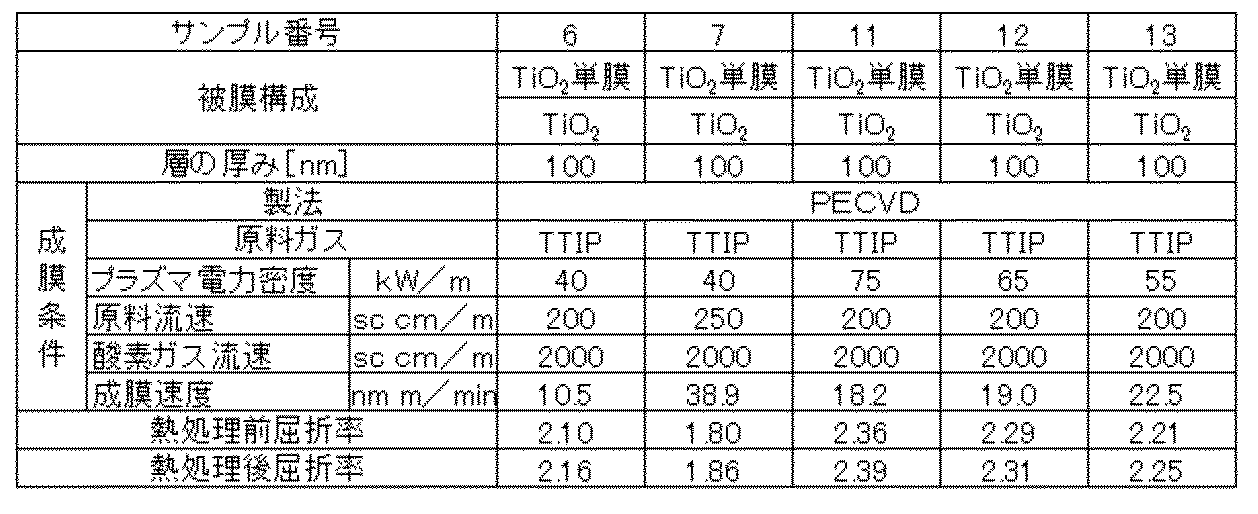
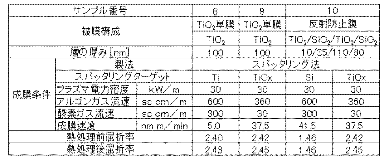

例1~5は本発明の実施例であり、熱処理後のヘイズ値が小さいことから、耐熱性が優れていることがわかる。
例6、7は低温プラズマCVD法によってTiO2膜を成膜したが、プラズマ電力密度が小さく、屈折率の高い膜が得られなかった比較例である。
例8~10はスパッタリング法によってTiO2膜を形成した比較例であり、熱処理によって被膜にクラック等が生じ、ヘイズ値が大きくなった。
例1、例11~13と例6を比較すると低温プラズマCVD法においてプラズマ電力密度が55kW/m以上のときに、屈折率が高いTiO2膜が得られることがわかる。
例6、7は低温プラズマCVD法によってTiO2膜を成膜したが、プラズマ電力密度が小さく、屈折率の高い膜が得られなかった比較例である。
例8~10はスパッタリング法によってTiO2膜を形成した比較例であり、熱処理によって被膜にクラック等が生じ、ヘイズ値が大きくなった。
例1、例11~13と例6を比較すると低温プラズマCVD法においてプラズマ電力密度が55kW/m以上のときに、屈折率が高いTiO2膜が得られることがわかる。
本発明によれば、熱処理によるクラック等の発生が抑制された耐熱性に優れ、かつ所望の光学的特性を有する高屈折率チタニア層を有する被膜付きガラス基板、およびこのような被膜付きガラス基板を製造する方法が提供できる。本発明は、可視光反射防止膜、赤外線反射膜、紫外線反射膜等の光学多層膜が形成される被膜付きガラス基板として有用である。
なお、2014年4月24日に出願された日本特許出願2014-090368号の明細書、特許請求の範囲、図面および要約書の全内容をここに引用し、本発明の開示として取り入れるものである。
なお、2014年4月24日に出願された日本特許出願2014-090368号の明細書、特許請求の範囲、図面および要約書の全内容をここに引用し、本発明の開示として取り入れるものである。
10A、10B…被膜付きガラス基板、11…ガラス基板、12…TiO2含有層、121…第1の高屈折率層、122…第2の高屈折率層、131…第1の低屈折率層、132…第2の低屈折率層、100…プラズマ源、110…電極群、110A…第1の電極、110B…第2の電極、110C…第3の電極、110D…第4の電極、130…交流電源、140…第1の極性用の配線、142…第2の極性用の配線、150(150A~150C)…空間、190…被処理体。
Claims (11)
- ガラス基板と被膜を有する被膜付きガラス基板であって、前記被膜は、TiO2含有率が90質量%以上、かつ波長632nmにおける屈折率が2.20以上の、低温プラズマCVD法により成膜されたTiO2含有層を、少なくとも1層含む被膜付きガラス基板。
- ガラス基板と被膜を有する被膜付きガラス基板であって、
前記被膜は、TiO2含有率が90質量%以上、かつ波長632nmにおける屈折率が2.20以上のTiO2含有層を、少なくとも1層含み、
前記TiO2含有層は、600℃以上650℃以下で熱処理されており、ヘイズ値が0.5%以下であることを特徴とする被膜付きガラス基板。 - ガラス基板と被膜を有する被膜付きガラス基板であって、
前記被膜は、TiO2含有率が90質量%以上、かつ波長632nmにおける屈折率が2.20以上のTiO2含有層を、少なくとも1層含み、
前記TiO2含有層は、650℃を超え700℃以下で熱処理されており、ヘイズ値が1%以下であることを特徴とする被膜付きガラス基板。 - 前記TiO2含有層の厚みが、10~1000nmである請求項1~3のいずれか1項に記載の被膜付きガラス基板。
- 前記被膜は、波長632nmにおける屈折率が、1.60以下の層と前記TiO2含有層が少なくとも1層ずつ交互に積層されてなる請求項1~4のいずれか1項に記載の被膜付きガラス基板。
- ガラス基板上に、アルコキシド系チタン材料、アミド系チタン材料およびハライド系チタン材料からなる群から選ばれる少なくとも1種を含む成膜原料を用いて、低温プラズマCVD法により、プラズマ電力密度が55kW/m以上、成膜速度が15~200nm・m/分の条件で、TiO2含有層を成膜する工程を具備する、
被膜付きガラス基板の製造方法。 - 前記TiO2含有層は、波長632nmにおける屈折率が2.20以上である請求項6記載の被膜付きガラス基板の製造方法。
- さらに、前記TiO2含有層を成膜する工程の後、前記TiO2含有層付きのガラス基板を熱処理する工程を有する請求項6または7に記載の被膜付きガラス基板の製造方法。
- 前記熱処理が、600℃~700℃の温度で行われる請求項8に記載の被膜付きガラス基板の製造方法。
- 前記成膜原料が、アルコキシド系チタン材料およびアミド系チタン材料からなる群から選ばれる少なくとも1種を含む請求項6~9のいずれか1項に記載の被膜付きガラス基板の製造方法。
- 前記成膜原料が、チタンテトライソプロポキシドを含む請求項10に記載の被膜付きガラス基板の製造方法。
Priority Applications (4)
| Application Number | Priority Date | Filing Date | Title |
|---|---|---|---|
| EP15783380.7A EP3135645B1 (en) | 2014-04-24 | 2015-04-21 | Coating film-equipped glass substrate, and method for producing coating film-equipped glass substrate |
| ES15783380T ES2821481T3 (es) | 2014-04-24 | 2015-04-21 | Sustrato de vidrio equipado con película de revestimiento y método para producir el sustrato de vidrio equipado con película de recubrimiento |
| PL15783380T PL3135645T3 (pl) | 2014-04-24 | 2015-04-21 | Podłoże szklane wyposażone w film powlekający i sposób wytwarzania podłoża szklanego wyposażonego w film powlekający |
| US15/298,646 US9988303B2 (en) | 2014-04-24 | 2016-10-20 | Coating film-equipped glass substrate, and method for producing coating film-equipped glass substrate |
Applications Claiming Priority (2)
| Application Number | Priority Date | Filing Date | Title |
|---|---|---|---|
| JP2014-090368 | 2014-04-24 | ||
| JP2014090368A JP2017105643A (ja) | 2014-04-24 | 2014-04-24 | 被膜付きガラス基板および被膜付きガラス基板の製造方法 |
Related Child Applications (1)
| Application Number | Title | Priority Date | Filing Date |
|---|---|---|---|
| US15/298,646 Continuation US9988303B2 (en) | 2014-04-24 | 2016-10-20 | Coating film-equipped glass substrate, and method for producing coating film-equipped glass substrate |
Publications (1)
| Publication Number | Publication Date |
|---|---|
| WO2015163331A1 true WO2015163331A1 (ja) | 2015-10-29 |
Family
ID=54332495
Family Applications (1)
| Application Number | Title | Priority Date | Filing Date |
|---|---|---|---|
| PCT/JP2015/062145 Ceased WO2015163331A1 (ja) | 2014-04-24 | 2015-04-21 | 被膜付きガラス基板および被膜付きガラス基板の製造方法 |
Country Status (6)
| Country | Link |
|---|---|
| US (1) | US9988303B2 (ja) |
| EP (1) | EP3135645B1 (ja) |
| JP (1) | JP2017105643A (ja) |
| ES (1) | ES2821481T3 (ja) |
| PL (1) | PL3135645T3 (ja) |
| WO (1) | WO2015163331A1 (ja) |
Cited By (1)
| Publication number | Priority date | Publication date | Assignee | Title |
|---|---|---|---|---|
| EP3385236A4 (en) * | 2015-12-03 | 2019-08-21 | AGC Inc. | GLASS PLATE WITH ANTIREFLEX FILM |
Families Citing this family (4)
| Publication number | Priority date | Publication date | Assignee | Title |
|---|---|---|---|---|
| US10862014B2 (en) * | 2015-11-12 | 2020-12-08 | Advanced Semiconductor Engineering, Inc. | Optical device package and method of manufacturing the same |
| CN108706889A (zh) * | 2018-05-08 | 2018-10-26 | 北京汉能光伏投资有限公司 | 一种镀膜板及其制备方法和一种太阳能组件 |
| JP2021003876A (ja) * | 2019-06-27 | 2021-01-14 | 凸版印刷株式会社 | 化粧シート |
| US20230054056A1 (en) * | 2019-12-19 | 2023-02-23 | Agc Glass Europe | Silicon oxide coated polymer films and low pressure pecvd methods for producing the same |
Citations (4)
| Publication number | Priority date | Publication date | Assignee | Title |
|---|---|---|---|---|
| JPH11181573A (ja) * | 1997-04-16 | 1999-07-06 | Sekisui Chem Co Ltd | 放電プラズマを利用した薄膜形成方法 |
| JP2003096569A (ja) * | 2001-09-25 | 2003-04-03 | Konica Corp | 薄膜形成方法、基材、及び薄膜形成装置 |
| JP2005107044A (ja) * | 2003-09-29 | 2005-04-21 | Konica Minolta Holdings Inc | ディスプレイ用フレネルレンズ |
| JP2008037667A (ja) * | 2006-08-02 | 2008-02-21 | Asahi Glass Co Ltd | 窓用合わせガラス |
Family Cites Families (6)
| Publication number | Priority date | Publication date | Assignee | Title |
|---|---|---|---|---|
| DE4114108C1 (ja) * | 1991-04-30 | 1991-12-19 | Schott Glaswerke, 6500 Mainz, De | |
| US6903512B2 (en) * | 2001-08-07 | 2005-06-07 | Konica Corporation | Half mirror film producing method and optical element comprising a half mirror film |
| US20070253051A1 (en) * | 2003-09-29 | 2007-11-01 | Kunihiko Ishihara | Optical Device |
| EP1845392A4 (en) | 2005-01-31 | 2009-06-03 | Asahi Glass Co Ltd | SUBSTRATE WITH ANTI-REFLECTION COATING |
| US20080102259A1 (en) * | 2006-10-26 | 2008-05-01 | Nikolov Anguel N | Oxide materials, articles, systems, and methods |
| JP2008201633A (ja) | 2007-02-21 | 2008-09-04 | Asahi Glass Co Ltd | 反射防止膜付きガラス板および窓用合わせガラス |
-
2014
- 2014-04-24 JP JP2014090368A patent/JP2017105643A/ja active Pending
-
2015
- 2015-04-21 PL PL15783380T patent/PL3135645T3/pl unknown
- 2015-04-21 ES ES15783380T patent/ES2821481T3/es active Active
- 2015-04-21 EP EP15783380.7A patent/EP3135645B1/en active Active
- 2015-04-21 WO PCT/JP2015/062145 patent/WO2015163331A1/ja not_active Ceased
-
2016
- 2016-10-20 US US15/298,646 patent/US9988303B2/en active Active
Patent Citations (4)
| Publication number | Priority date | Publication date | Assignee | Title |
|---|---|---|---|---|
| JPH11181573A (ja) * | 1997-04-16 | 1999-07-06 | Sekisui Chem Co Ltd | 放電プラズマを利用した薄膜形成方法 |
| JP2003096569A (ja) * | 2001-09-25 | 2003-04-03 | Konica Corp | 薄膜形成方法、基材、及び薄膜形成装置 |
| JP2005107044A (ja) * | 2003-09-29 | 2005-04-21 | Konica Minolta Holdings Inc | ディスプレイ用フレネルレンズ |
| JP2008037667A (ja) * | 2006-08-02 | 2008-02-21 | Asahi Glass Co Ltd | 窓用合わせガラス |
Non-Patent Citations (1)
| Title |
|---|
| See also references of EP3135645A4 * |
Cited By (2)
| Publication number | Priority date | Publication date | Assignee | Title |
|---|---|---|---|---|
| EP3385236A4 (en) * | 2015-12-03 | 2019-08-21 | AGC Inc. | GLASS PLATE WITH ANTIREFLEX FILM |
| US10654746B2 (en) | 2015-12-03 | 2020-05-19 | AGC Inc. | Glass plate with antireflection film |
Also Published As
| Publication number | Publication date |
|---|---|
| US9988303B2 (en) | 2018-06-05 |
| EP3135645A1 (en) | 2017-03-01 |
| EP3135645A4 (en) | 2018-01-10 |
| ES2821481T3 (es) | 2021-04-26 |
| EP3135645B1 (en) | 2020-08-05 |
| JP2017105643A (ja) | 2017-06-15 |
| PL3135645T3 (pl) | 2020-12-14 |
| US20170036948A1 (en) | 2017-02-09 |
Similar Documents
| Publication | Publication Date | Title |
|---|---|---|
| JP6814853B2 (ja) | 光学フィルタおよびその形成方法 | |
| CN102985589B (zh) | 用于制造在触摸面板中使用的透明主体的方法与系统 | |
| KR102051328B1 (ko) | 가스 배리어성 필름 | |
| JP4269261B2 (ja) | 透明ガスバリアフィルムの製造方法 | |
| WO2015163331A1 (ja) | 被膜付きガラス基板および被膜付きガラス基板の製造方法 | |
| US20110194181A1 (en) | Film forming method for antireflection film, antireflection film, and film forming device | |
| CN105874544B (zh) | 透明导电膜及其制造方法 | |
| WO2004038061A1 (ja) | 多層膜付き基板とその製造方法 | |
| TW202009529A (zh) | 紅外帶通濾波器 | |
| CN111025434A (zh) | 防反射玻璃 | |
| TW201531582A (zh) | 層合薄膜及撓曲性電子裝置 | |
| JP2006068992A (ja) | ガスバリア性フィルム | |
| JP2013541490A (ja) | ガラスを被覆する方法 | |
| JP4837271B2 (ja) | 反射防止膜の形成方法 | |
| CN119414500A (zh) | 多功能膜及其制备方法、应用以及透光面板 | |
| JP5123785B2 (ja) | 反射防止膜の成膜方法及び反射防止膜 | |
| JP4899863B2 (ja) | 薄膜形成装置及び薄膜形成方法 | |
| KR101334725B1 (ko) | 터치 스크린 패널용 투명 도전성 필름 및 그 제조방법 | |
| TWI399456B (zh) | 導電膜製作設備及用於在其中處理基板之方法 | |
| JP2004042412A (ja) | 透明ガスバリア性薄膜被覆フィルム | |
| JP2022036766A (ja) | Ndフィルタ及びndフィルタの製造方法 | |
| JP2004223769A (ja) | 透明積層フィルム、反射防止フィルム及びそれを用いた偏光板、液晶表示装置 | |
| JP7162867B2 (ja) | Ndフィルタ及びその製造方法 | |
| JP7307420B1 (ja) | 反射防止膜 | |
| WO2013176132A1 (ja) | ガラス基板を製造する方法およびガラス基板 |
Legal Events
| Date | Code | Title | Description |
|---|---|---|---|
| 121 | Ep: the epo has been informed by wipo that ep was designated in this application |
Ref document number: 15783380 Country of ref document: EP Kind code of ref document: A1 |
|
| NENP | Non-entry into the national phase |
Ref country code: DE |
|
| REEP | Request for entry into the european phase |
Ref document number: 2015783380 Country of ref document: EP |
|
| WWE | Wipo information: entry into national phase |
Ref document number: 2015783380 Country of ref document: EP |
|
| NENP | Non-entry into the national phase |
Ref country code: JP |