WO2015165094A1 - 一种接收机 - Google Patents
一种接收机 Download PDFInfo
- Publication number
- WO2015165094A1 WO2015165094A1 PCT/CN2014/076643 CN2014076643W WO2015165094A1 WO 2015165094 A1 WO2015165094 A1 WO 2015165094A1 CN 2014076643 W CN2014076643 W CN 2014076643W WO 2015165094 A1 WO2015165094 A1 WO 2015165094A1
- Authority
- WO
- WIPO (PCT)
- Prior art keywords
- signal
- polarization
- output terminal
- polarization direction
- combined
- Prior art date
- Legal status (The legal status is an assumption and is not a legal conclusion. Google has not performed a legal analysis and makes no representation as to the accuracy of the status listed.)
- Ceased
Links
Classifications
-
- H—ELECTRICITY
- H04—ELECTRIC COMMUNICATION TECHNIQUE
- H04B—TRANSMISSION
- H04B10/00—Transmission systems employing electromagnetic waves other than radio-waves, e.g. infrared, visible or ultraviolet light, or employing corpuscular radiation, e.g. quantum communication
- H04B10/60—Receivers
- H04B10/61—Coherent receivers
- H04B10/616—Details of the electronic signal processing in coherent optical receivers
- H04B10/6162—Compensation of polarization related effects, e.g., PMD, PDL
-
- H—ELECTRICITY
- H04—ELECTRIC COMMUNICATION TECHNIQUE
- H04B—TRANSMISSION
- H04B10/00—Transmission systems employing electromagnetic waves other than radio-waves, e.g. infrared, visible or ultraviolet light, or employing corpuscular radiation, e.g. quantum communication
- H04B10/60—Receivers
- H04B10/66—Non-coherent receivers, e.g. using direct detection
- H04B10/69—Electrical arrangements in the receiver
- H04B10/697—Arrangements for reducing noise and distortion
-
- H—ELECTRICITY
- H04—ELECTRIC COMMUNICATION TECHNIQUE
- H04B—TRANSMISSION
- H04B10/00—Transmission systems employing electromagnetic waves other than radio-waves, e.g. infrared, visible or ultraviolet light, or employing corpuscular radiation, e.g. quantum communication
-
- H—ELECTRICITY
- H04—ELECTRIC COMMUNICATION TECHNIQUE
- H04B—TRANSMISSION
- H04B10/00—Transmission systems employing electromagnetic waves other than radio-waves, e.g. infrared, visible or ultraviolet light, or employing corpuscular radiation, e.g. quantum communication
- H04B10/07—Arrangements for monitoring or testing transmission systems; Arrangements for fault measurement of transmission systems
- H04B10/075—Arrangements for monitoring or testing transmission systems; Arrangements for fault measurement of transmission systems using an in-service signal
- H04B10/079—Arrangements for monitoring or testing transmission systems; Arrangements for fault measurement of transmission systems using an in-service signal using measurements of the data signal
- H04B10/0795—Performance monitoring; Measurement of transmission parameters
- H04B10/07951—Monitoring or measuring chromatic dispersion or PMD
-
- H—ELECTRICITY
- H04—ELECTRIC COMMUNICATION TECHNIQUE
- H04B—TRANSMISSION
- H04B10/00—Transmission systems employing electromagnetic waves other than radio-waves, e.g. infrared, visible or ultraviolet light, or employing corpuscular radiation, e.g. quantum communication
- H04B10/60—Receivers
- H04B10/61—Coherent receivers
- H04B10/614—Coherent receivers comprising one or more polarization beam splitters, e.g. polarization multiplexed [PolMux] X-PSK coherent receivers, polarization diversity heterodyne coherent receivers
-
- H—ELECTRICITY
- H04—ELECTRIC COMMUNICATION TECHNIQUE
- H04B—TRANSMISSION
- H04B10/00—Transmission systems employing electromagnetic waves other than radio-waves, e.g. infrared, visible or ultraviolet light, or employing corpuscular radiation, e.g. quantum communication
- H04B10/60—Receivers
- H04B10/61—Coherent receivers
- H04B10/615—Arrangements affecting the optical part of the receiver
- H04B10/6151—Arrangements affecting the optical part of the receiver comprising a polarization controller at the receiver's input stage
Definitions
- the present invention relates to the field of communications, and in particular, to a receiver.
- BACKGROUND [02] With the continuous development of network applications, people's requirements for communication capacity are increasing, and the transmission rate of optical communication networks is exponentially increasing. Whether it is a low-cost direct-detection optical communication system or a relatively high-cost coherent detection communication system based on a coherent receiver, a lower cost is required to achieve a larger capacity transmission.
- Direct detection of optical signals in optical communication systems has beat frequency interference between different frequency components of the signal itself, that is, Signal-to-Signal Beat Interference (SSBI), thereby reducing the direct detection of optical communication systems. Transmission performance.
- SSBI Signal-to-Signal Beat Interference
- the receiver sends the received optical signal to the DSP processing unit.
- the DSP processing unit calculates the size of the SSBI in the optical signal by a certain algorithm, and subtracts the SSBI from the optical signal according to the calculation result, thereby obtaining an optical signal for eliminating the SSBI.
- a receiver which can realize reception of a dual-polarized signal and can eliminate SSBI in a dual-polarized signal.
- a receiver comprising:
- a signal acquisition unit configured to receive a dual-polarization signal and a local oscillator, and perform polarization splitting processing on the dual-polarization signal and the local oscillator, respectively, to obtain signals of the dual-polarized signals in the X and Y polarization directions, And a signal of the local oscillator in the X and Y polarization directions, respectively;
- a signal diversity unit coupled to the signal acquisition unit, for coupling the signal of the dual polarization signal in the X polarization direction and the signal of the local oscillator in the X polarization direction to obtain different phase shifting a coupling signal in the X polarization direction; also used for the signal and local oscillator in the Y polarization direction of the dual polarization signal in Y The signal in the polarization direction is coupled to obtain a coupled signal in the Y polarization direction with different phase shifts;
- a signal combining unit coupled to the signal diversity unit, for combining a coupled signal in the X polarization direction and a coupled signal in the Y polarization direction as a group to obtain a combined signal, Converting the combined signal into an electrical signal;
- a digital signal acquiring unit connected to the signal combining unit, for receiving an electrical signal output by the signal combining unit, generating a digital signal of the electrical signal of the dual polarized signal in the X polarization direction according to the received electrical signal, and dual polarization A digital signal whose signal is an electrical signal in the Y polarization direction.
- the signal acquiring unit includes:
- the first polarization beam splitter PBS receives the dual polarization signal, the first output end of the first PBS outputs the signal of the dual polarization signal in the X polarization direction, and the second output end of the first PBS Outputting a signal of the dual polarized signal in the Y polarization direction;
- the second PBS receives the local oscillator, the first output end of the second PBS outputs a signal of the local oscillator in the X polarization direction, and the second output end of the second PBS outputs the local oscillator in the Y polarization Signal in the direction.
- the signal diversity unit includes:
- the first polarization-maintaining coupler PMOC the first input terminal is connected to the first output end of the first PBS, the signal of the dual polarization signal is received in the X polarization direction, and the second input terminal is connected to the second PBS
- the first output end receives the signal of the local oscillator in the X polarization direction, and the first output end is connected to the input end of the second PMOC, to the second
- the PMOC outputs a first signal, the first signal is, and the second output is connected to the first attenuation - J
- Input end of the device outputting a second signal to the first attenuator, the second signal is;
- a first output end of the PMOC outputs a first coupled signal, the first coupled signal is 2 2 , a second
- the output terminal outputs a second coupled signal, the second coupled signal is 2 2 ; the output of the first attenuator
- the terminal outputs a third coupled signal, and the third coupled signal is 2 2 ;
- the third PMOC the first input end is connected to the second output end of the first PBS, the signal of the dual polarization signal is received in the Y polarization direction, and the second input end is connected to the second output end of the second PBS Receiving a signal of the local oscillator in the Y polarization direction, the first output end is connected to the input end of the second attenuator, and the third output is output to the second attenuator
- the third signal is ⁇ " ⁇ the second output is connected to the input end of the fourth PMOC,
- the fourth PMOC outputs a fourth signal, and the fourth signal is ; the output of the second attenuator is lost
- a fourth coupled signal wherein the fourth coupled signal is 2 " 2 , the first output end of the fourth PMOC outputs a fifth coupled signal, the fifth coupled signal is ⁇ + " 7 ⁇ , and the second output is outputted sixth.
- a coupled signal, the sixth coupled signal is 2 Jy 2 ⁇ ; [18] ⁇ is a signal of a double-polarized signal in the x- polarization direction, and £ is a signal of a dual-polarized signal in a Y-polarized direction, and the local oscillator is in an X-polarized The signal in the direction, the signal of the local oscillator in the direction of ⁇ polarization.
- the signal combining unit includes:
- the first polarization combiner PBC the first input end is connected to the first output end of the second PMOC, receives the first coupling signal, the second input end is connected to the output end of the second attenuator, and receives the fourth coupled signal, The output end is connected to the input end of the first photodetector PD, and outputs a first combined signal to the first PD, where the first combined signal is added by the first coupled signal and the fourth coupled signal;
- the second PBC the first input is connected to the second output of the second PMOC, receives the second coupled signal, the second input is connected to the first output of the fourth PMOC, receives the fifth coupled signal, and the output is connected
- the input end of the second PD outputs a second combined signal to the second PD, where the second combined signal is added to the second coupled signal and the fifth coupled signal;
- the third PBC the first input is connected to the output of the first attenuator, the third coupled signal is received, the second input is connected to the second output of the fourth PMOC, the sixth coupled signal is received, and the output is connected.
- the input end of the third PD outputs a third combined signal to the third PD, where the third combined signal is added by the third coupled signal and the sixth coupled signal;
- the output end outputs an electrical signal of the first combined signal
- the output end outputs an electrical signal of the second combined signal
- the third PD the output end outputs an electrical signal of the third combined signal.
- the digital signal acquiring unit includes:
- a first converter configured to convert the received electrical signals of the combined signals into digital signals of the combined signals, respectively;
- the first processor is connected to the output end of the first converter, and the digital signal for outputting the first combined signal of the first converter to the electrical signal of the third combined signal is sequentially Subtracting, a digital signal of an electrical signal of the dual polarization signal in the X polarization direction and a digital signal of the electrical signal of the dual polarization signal in the Y polarization direction are obtained.
- the signal combining unit is further configured to:
- the digital signal acquisition unit includes:
- a second converter for converting the electrical signal of the dual polarized signal in the X polarization direction and the electrical signal of the dual polarization signal in the Y polarization direction into a digital signal, respectively.
- the signal merging unit further includes:
- the first subtractor the positive input terminal is connected to the output end of the first PD, the electrical signal of the first combined signal is input, the negative input terminal is connected to the output end of the second PD, and the electrical signal of the second combined signal is input, and the output end is Outputting an electrical signal of the dual polarized signal in the Y polarization direction;
- the second subtractor the positive input is connected to the output of the second PD, the electrical signal of the second combined signal is input, the negative input is connected to the output of the third PD, and the electrical signal of the third combined signal is input, the output is An electrical signal of the dual polarized signal in the X polarization direction is output.
- the signal diversity unit includes:
- a first optical hybrid a first input connected to the first output of the first PBS, receiving a signal of the dual polarized signal in the X polarization direction, and a second input connected to the first of the second PBS
- the output end receives the signal of the local oscillator in the X polarization direction, the first output end is connected to the input end of the fifth PMOC, and the fifth PMOC is outputted to the first jE —
- a fifth signal wherein the fifth signal is an input end of the second output three attenuator, and a sixth signal is output to the third attenuator, wherein the sixth signal is , the third output is connected to the third
- the input end of C outputs a seventh signal to the sixth PMOC, and the seventh signal is
- the fourth output is connected to the input end of the fourth attenuator, and the fourth output is output to the fourth attenuator ⁇ 3 ⁇ 4
- the eighth signal is The first output of the fifth PMOC outputs the seventh coupling letter
- the seventh coupled signal is 2 2
- the second output end outputs an eighth coupled signal
- the coupled signal is 2 2 ; the output of the third attenuator outputs a ninth coupled signal, the ninth coupling
- the signal is 2 2 ; the first output of the sixth PMOC outputs a tenth coupled signal, the tenth coupling
- the second output terminal outputs an eleventh coupled signal, wherein the eleventh coupled signal is 2; the output end of the fourth attenuator outputs a twelfth coupled signal, the twelfth coupled signal 2 ;
- a second optical hybrid a first input end connected to the second output end of the first PBS, receiving a signal of the dual polarized signal in the Y polarization direction, and a second input end connected to the second PBS second
- the output end receives the signal of the local oscillator in the Y polarization direction
- the input end of the first five attenuator outputs a ninth signal to the fifth attenuator
- the ninth signal is ⁇ "
- the second output is connected to the input end of the seventh PMOC, and outputs a tenth signal to the seventh PMOC.
- the tenth signal is that the third output is connected to the input end of the sixth attenuator, and the eleventh output is output to the sixth attenuator.
- Signal, the eleventh signal is
- the fourth output is connected to the input end of the eighth PMOC, and is output to the eighth PMOC.
- the output of the fifth attenuator outputs a tenth combined signal
- the thirteenth coupled signal is The first output end of the seventh PMOC outputs a fourteenth coupling signal, the fourteenth coupling signal is ⁇ + ⁇ " 7 " ⁇ , and the second output terminal outputs a fifteenth coupling signal, the fifteenth coupling signal Outputting a sixteenth coupling signal for the output of the second Jy 2 sixth attenuator, the sixteenth coupling signal being the first output of the eighth PMOC of the Esy +1 i jELOy output a coupling signal, the seventeenth coupling signal is " ⁇ El0y , the second output terminal outputs an eighteenth coupling signal, and the eighteenth coupling signal is ⁇ 2jEl0y ;
- the signal combining unit includes:
- the fourth PBC the first input is connected to the first output of the fifth PMOC, receives the seventh coupled signal, the second input is connected to the output of the fifth attenuator, receives the thirteenth coupled signal, and the output is connected An input end of the fourth PD outputs a fourth combined signal to the fourth PD, where the fourth combined signal is added to the seventh coupled signal and the thirteenth coupled signal;
- the fifth PBC the first input terminal is connected to the second output end of the fifth PMOC, and receives the eighth coupling signal
- the second input terminal is connected to the first output end of the seventh PMOC, and receives the fourteenth coupled signal, and the output end Connecting the input end of the fifth PD, and outputting a fifth combined signal to the fifth PD, where the fifth combined signal is added to the eighth coupled signal and the fourteenth coupled signal;
- the sixth PBC the first input terminal is connected to the output end of the third attenuator, receives the ninth coupling signal, the second input terminal is connected to the second output end of the seventh PMOC, receives the fifteenth coupling signal, and the output terminal is connected An input end of the sixth PD, outputting a sixth combined signal to the sixth PD, where the sixth combined signal is added to the ninth coupled signal and the fifteenth coupled signal;
- the seventh PBC the first input is connected to the first output of the sixth PMOC, receives the tenth coupled signal, the second input is connected to the output of the fourth attenuator, receives the sixteenth coupled signal, and the output is connected And inputting, to the seventh PD, a seventh combined signal, where the seventh combined signal is added by the tenth coupled signal and the sixteenth coupled signal;
- the eighth PBC the first input is connected to the second output of the sixth PMOC, and receives the eleventh coupled signal
- the second input is connected to the first output of the eighth PMOC, and receives the seventeenth coupled signal
- the output is connected to the input end of the eighth PD, and outputs an eighth combined signal to the eighth PD, where the eighth combined signal is added by the eleventh coupled signal and the seventeenth coupled signal;
- the ninth PBC the first input is connected to the output of the fourth attenuator, the twelfth coupled signal is received, the second input is connected to the second output of the eighth PMOC, and the eighteenth coupled signal is received, the output end Connecting the ninth PD Inputting, outputting a ninth combined signal to the ninth PD, wherein the ninth combined signal is added to the twelfth coupled signal and the eighteenth coupled signal;
- the fifth PD the output end outputs an electrical signal of the fifth combined signal
- the sixth PD the output end outputs an electrical signal of the sixth combined signal
- the seventh PD the output end outputs an electrical signal of the seventh combined signal
- the eighth PD the output end outputs an electrical signal of the eighth combined signal
- the ninth PD the output terminal outputs an electrical signal of the ninth combined signal.
- the digital signal acquiring unit includes:
- a third converter configured to separately convert the received electrical signals of the combined signals into digital signals
- a second processor wherein the second processor is connected to an output end of the second converter, and is configured to convert the digital signal of the electrical signal of the fourth combined signal output by the second converter and the electrical signal of the fifth combined signal
- the digital signal is subtracted to obtain a digital signal of the orthogonal component electrical signal of the dual polarization signal in the Y polarization direction; the digital signal of the electrical signal of the fifth combined signal output by the second converter and the electrical signal of the sixth combined signal
- the digital signal is subtracted to obtain a digital signal of the orthogonal component electrical signal of the dual polarization signal in the X polarization direction; the digital signal of the electrical signal of the seventh combined signal output by the second converter and the electrical signal of the eighth combined signal
- the digital signal is subtracted to obtain a digital signal of the in-phase component electrical signal of the dual-polarized signal in the Y-polarized direction; the digital signal of the electrical signal of the eighth combined signal outputted by the second converter and the digital signal of the electrical signal of the ninth combined signal Subtracting, a
- the signal combining unit is further configured to:
- the digital signal acquisition unit includes:
- a fourth converter an electrical signal for in-phase component of the dual-polarized signal in the Y-polarization direction, an electrical signal of the in-phase component of the dual-polarized signal in the X-polarization direction, and a quadrature component of the dual-polarized signal in the Y-polarization direction
- the electrical signals of the orthogonal components of the X and polarization signals in the X polarization direction are respectively converted into digital signals.
- the signal merging unit further includes:
- the third subtractor the positive input terminal is connected to the output end of the fourth PD, the electrical signal of the fourth combined signal is input, the negative input terminal is connected to the output end of the fifth PD, and the electrical signal of the fifth combined signal is input, and the output end is Outputting an electrical signal of a quadrature polarized signal orthogonal component in the Y polarization direction;
- the fourth subtractor the positive input terminal is connected to the output end of the fifth PD, the electrical signal of the fifth combined signal is input, the negative input terminal is connected to the output end of the sixth PD, and the electrical signal of the sixth combined signal is input, and the output is output. Outputting an electrical signal of a quadrature polarization component orthogonally in the X polarization direction;
- the fifth subtractor the positive input terminal is connected to the output end of the seventh PD, the electrical signal of the seventh combined signal is input, the negative input terminal is connected to the output end of the eighth PD, and the electrical signal of the eighth combined signal is input, and the output end is Outputting an electrical signal of the in-phase component of the dual polarization signal in the Y polarization direction;
- the sixth subtractor the positive input terminal is connected to the output end of the eighth PD, the electrical signal of the eighth combined signal is input, the negative input terminal is connected to the output end of the ninth PD, and the electrical signal of the ninth combined signal is input, and the output end is An electrical signal of the same phase component of the dual polarization signal in the X polarization direction is output.
- the method further includes:
- a third processor a digital signal for receiving an electrical signal of the dual polarization signal in the X polarization direction and a digital signal of the electrical signal of the dual polarization signal in the Y polarization direction, and powering the X polarization direction by the following matrix
- the digital signal of the signal and the digital signal of the electrical signal in the Y polarization direction are processed to obtain a demodulation result of the dual polarization signal:
- a receiver comprising:
- a signal acquisition unit configured to receive a dual polarization signal, and perform polarization splitting processing on the dual polarization signal to obtain signals of the dual polarization signals in X and Y polarization directions, respectively;
- a signal conversion unit coupled to the signal acquisition unit, for respectively separating the dual polarization signals in X and The signals in the Y polarization direction are respectively converted into electrical signals;
- a digital signal conversion unit coupled to the signal conversion unit, for converting an electrical signal output by the signal conversion unit into a digital signal
- the data of every 3 frames in the dual-polarized signal is one unit, and the structure of the three-frame data includes: and “ ⁇ , ⁇ ⁇ and ⁇ , ⁇ and ⁇ ⁇ ⁇ are double-polarized signals in the ⁇ polarization direction
- the signal on the signal is the signal of the double-polarized signal in the ⁇ polarization direction.
- the signal acquiring unit includes:
- the input end of the third polarization beam splitter PBS receives the dual polarization signal, the first output end of the third PBS outputs the signal of the dual polarization signal in the X polarization direction, and the second of the third PBS The output outputs a signal of the dual polarization signal in the ⁇ polarization direction.
- the signal conversion unit includes:
- the tenth photodetector PD the input end is connected to the first output end of the third PBS, receives the signal of the dual polarized signal in the X polarization direction, and the output end outputs the signal of the double polarized signal in the X polarization direction.
- the eleventh PD the input end is connected to the second output end of the third PBS, receives the signal of the double polarized signal in the Y polarization direction, and the output end outputs the electric signal of the signal of the double polarized signal in the Y polarization direction.
- the digital signal conversion unit includes:
- a tenth analog-to-digital converter ADC wherein the input end is connected to the output end of the tenth PD, and converts the electrical signal of the signal of the dual-polarized signal in the X-polarization direction into a digital signal;
- the eleventh ADC the input end is connected to the output end of the eleventh PD, and converts the electrical signal of the signal of the dual polarized signal in the Y polarization direction into a digital signal.
- a signal acquiring unit is configured to receive a dual-polarized signal and a local oscillator, and perform polarization splitting processing on the dual-polarized signal and the local oscillator, respectively, to obtain the dual-polarized signal respectively.
- a signal diversity unit coupled to the signal acquisition unit for using the dual polarization signal in the X polarization direction
- the signal and the local oscillator are coupled in the X polarization direction to obtain a coupled signal in the X polarization direction with different phase shifts; and the signal and the local oscillator in the Y polarization direction of the dual polarized signal are also in Y
- the signals in the polarization direction are coupled to obtain a coupling signal in the Y polarization direction with different phase shifts;
- a signal combining unit is connected to the signal diversity unit for coupling a coupling signal in the X polarization direction with Y polarization
- the coupled signals in the direction are combined as a group to obtain a combined signal, and the combined signal is converted into an electrical signal.
- the digital signal acquiring unit is connected to the signal combining unit 130 for receiving the combined signal of the signal combining unit.
- the electrical signal generates a digital signal of the electrical signal of the dual polarized signal in the X polarization direction and a digital signal of the electrical signal of the dual polarized signal in the Y polarization direction according to the received electrical signal.
- FIG. 1 is a schematic structural diagram of an implementation of a receiver according to an embodiment of the present invention.
- FIG. 2 is a schematic structural diagram of a second implementation of a receiver according to an embodiment of the present invention.
- FIG. 2A is a schematic structural diagram of a third implementation of a receiver according to an embodiment of the present invention.
- FIG. 3 is a schematic diagram of a fourth implementation structure of a receiver according to an embodiment of the present invention.
- FIG. 4 is a schematic diagram of a fifth implementation structure of a receiver according to an embodiment of the present invention.
- 4A is a schematic structural diagram of an implementation of an optical hybrid according to an embodiment of the present invention.
- FIG. 4B is a schematic diagram of a sixth implementation structure of a receiver according to an embodiment of the present invention.
- FIG. 5 is a schematic structural diagram of a seventh implementation of a receiver according to an embodiment of the present invention.
- FIG. 6 is a schematic diagram of an eighth implementation structure of a receiver according to an embodiment of the present invention. detailed description
- FIG. 1 is a schematic structural diagram of a receiver according to an embodiment of the present invention.
- the receiver 100 includes:
- the signal acquisition unit 110 is configured to receive the dual polarization signal and the local oscillator, and perform polarization splitting processing on the dual polarization signal and the local oscillator, respectively, to obtain signals of the dual polarization signals in the X and Y polarization directions, respectively. And the signals of the local oscillator in the X and Y polarization directions, respectively;
- the signal diversity unit 120 is connected to the signal acquisition unit 110 for coupling the signal of the dual polarization signal in the X polarization direction and the signal of the local oscillator in the X polarization direction to obtain different shifts.
- a coupling signal in the X polarization direction of the phase is also used for coupling the signal of the dual polarization signal in the Y polarization direction and the signal of the local oscillator in the Y polarization direction to obtain a Y polarization direction with different phase shifts Collaborative unit number;
- the signal combining unit 130 is connected to the signal diversity unit 120 for combining a coupled signal in the X polarization direction and a coupled signal in the Y polarization direction as a group to obtain a combined signal. Converting the combined signal into an electrical signal;
- the digital signal acquiring unit 140 is connected to the signal combining unit 130 for receiving an electrical signal of the combined signal output by the signal combining unit 130, and generating an electrical signal of the dual polarized signal in the X polarization direction according to the received electrical signal.
- the digital signal and the digital signal of the electrical signal of the dual polarized signal in the Y polarization direction are connected to the signal combining unit 130 for receiving an electrical signal of the combined signal output by the signal combining unit 130, and generating an electrical signal of the dual polarized signal in the X polarization direction according to the received electrical signal.
- the digital signal and the digital signal of the electrical signal of the dual polarized signal in the Y polarization direction are connected to the signal combining unit 130 for receiving an electrical signal of the combined signal output by the signal combining unit 130, and generating an electrical signal of the dual polarized signal in the X polarization direction according to the received electrical signal.
- the signal acquiring unit is configured to receive the dual-polarized signal and the local oscillator, and perform polarization splitting processing on the dual-polarized signal and the local oscillator, respectively, to obtain the dual-polarized signal in the X and Y polarization, respectively.
- a signal in the direction and a signal of the local oscillator in the X and Y polarization directions, respectively; a signal diversity unit coupled to the signal acquisition unit for the signal and the local oscillator in the X polarization direction of the dual polarization signal
- the signal in the X polarization direction is coupled to obtain a coupled signal in the X polarization direction with different phase shifts; and is also used for the signal of the dual polarized signal in the Y polarization direction and the signal of the local oscillator in the Y polarization direction.
- a signal combining unit coupled to the signal diversity unit for coupling a coupled signal in the X polarization direction with a Y polarization direction
- the coupled signals are combined as a group to obtain a combined signal, and the combined signal is converted into an electrical signal; the digital signal acquiring unit, and
- the signal combining unit is connected, and is configured to receive an electrical signal of the combined signal output by the signal combining unit, generate a digital signal of the electrical signal of the dual polarized signal in the X polarization direction according to the received electrical signal, and generate an electrical signal of the dual polarized signal in the Y polarization direction.
- the reception of the dual-polarized signal is realized, and the processing of the dual-polarized signal and the local oscillator by the signal acquisition unit, the signal diversity unit and the signal combining unit eliminates the SSBI in the dual-polarized signal; moreover, the receiver is implemented by hardware, the device The cost is not high, and the processing speed is fast, which can meet the real-time application.
- a signal acquisition unit is formed by a first polarization splitter (PBS) and a second PBS 212.
- the first polarization-maintaining coupler (PMOC) 221-the fourth PMOC 224, the first attenuator 231, and the second attenuator 232 constitute a signal diversity unit, and the first partial bias a PBC (Polarization Beam Combiner) 241 to a third PBC 243, a first photodetector (PD), a third PD 253, a first subtractor 261, and a second subtractor 262 constitute a signal combining unit.
- a first analog-to-digital converter (ADC) and a second ADC 272 constitute a digital signal acquisition unit;
- the input end of the first PBS 211 receives the dual polarization signal, and performs polarization splitting processing on the dual polarization signal.
- the first output end of the first PBS 211 is connected to the first input end of the first PMOC221, and the dual polarization signal is outputted to the first PMOC 221.
- a signal in the X polarization direction a second output end of the first PBS 211 is connected to the first input end of the third PMOC 223, and a signal of the dual polarization signal in the Y polarization direction is output to the third PMOC 223;
- the input end of the second PBS 212 receives the local oscillator, and performs polarization splitting processing on the local oscillator.
- the first output end of the second PBS 212 is connected to the second input end of the first PMOC221, and the local oscillator is output to the first PMOC221 in the X polarization direction.
- the signal on the second PBS 212 is connected to the second input end of the third PMOC 223, and outputs the signal of the local oscillator in the Y polarization direction to the third PMOC 223;
- the first PMOC 221 is configured to couple the signal of the input dual-polarized signal in the X-polarization direction and the signal of the local oscillator in the X-polarization direction, and the first output end of the first PMOC 221 is connected to the second PMOC 222.
- the first terminal outputs a first signal to the second PMOC 222, and the first signal is 2 ; the second output end of the first PMOC 221 is connected to the input end of the first attenuator 231, and outputs a second signal to the first attenuator 231.
- the second signal is ⁇ /2 V2 ; ⁇ ⁇ is the signal of the double-polarized signal in the X-polarization direction, and E LOx is the signal of the local oscillator in the X-polarization direction;
- the second PMOC 222 is configured to perform a coupling process on the input first signal, the first output end of the second PMOC 222 is connected to the first input end of the first PBC 241, and the first PBC 241 is outputting the first coupled signal, the first The coupled signal ⁇ is _/ + ⁇ , and the second output is connected to the first input of the second PBC 242, to the second
- the PBC 242 outputs a second coupled signal, the second coupled signal is _ + _/ ⁇ ⁇ ⁇ ; the first attenuator
- the output end of the first attenuator 231 is connected to the first input end of the third PBC 243, and the third coupled signal is output to the third PBC 243, where the third coupled signal is
- the third PMOC 223 is used to input the signal of the dual polarized signal in the Y polarization direction and the local oscillator in the Y bias The signal in the direction of the vibration is coupled.
- the first output of the third PMOC 223 is connected to the input of the second attenuator 232, and the third signal is output to the second attenuator 232.
- the third signal is ⁇ , and the third PMOC223
- the second output is connected to the input end of the fourth PMOC 224, and outputs a fourth signal to the fourth PMOC 224, where the fourth signal is a signal of the dual polarized signal in the ⁇ polarization direction,
- E LOx is the signal of the local oscillator in the Y polarization direction
- the second attenuator 232 is configured to perform power attenuation processing on the input third signal, the output end of the second attenuator 232 is connected to the second input end of the first PBC 241, and the fourth coupled signal is output to the first PBC 241.
- the fourth coupled signal ⁇ is a fourth PMOC 224 for coupling the fourth signal
- the first output of the fourth PMOC 224 is connected to the second input of the second PBC 242, and the fifth coupled signal is output to the second PBC 242.
- the fifth coupled signal is + _/ ⁇ , and the second output of the fourth PMOC 224 is connected to the third.
- the second input end of the PBC 243 outputs a sixth coupling signal to the third PBC 243, where the sixth coupling signal is ⁇
- the first PBC 241 is configured to perform polarization combining processing on the first coupled signal and the fourth coupled signal, the output end of the first PBC 241 is connected to the input end of the first PD 251, and the first combined signal is output to the first PD 251, The first combined signal is added by the first coupled signal and the fourth coupled signal, specifically, the first combined signal;
- the second PBC 242 is configured to perform polarization combining processing on the second coupled signal and the fifth coupled signal, the output end of the second PBC 242 is connected to the input end of the second PD 252, and the second combined signal is output to the second PD 252.
- the second combined signal is added by the second coupled signal and the fifth coupled signal, specifically, the second combined signal
- the third PBC 243 is configured to perform polarization combining processing on the third coupled signal and the sixth coupled signal, the output end of the third PBC 243 is connected to the input end of the third PD 253, and the third combined signal is output to the third PD 253.
- the third combined signal is a third coupled signal and a sixth coupled signal added, specifically, a third combined signal
- the first PD 251 is configured to convert the first combined signal into an electrical signal, and the output end is connected to the positive input end of the first subtractor 261, and output the electrical signal of the first combined signal to the first subtractor 261;
- First combined signal electrical signal Re indicates that the real part is taken;
- the second PD 252 is configured to convert the second combined signal into an electrical signal, and the output ends are respectively connected to the negative input terminal of the first subtractor 261 and the positive input terminal of the second subtractor 262, to the first subtractor 261 and The second subtractor 262 outputs an electrical signal of the second combined signal; specifically, the electrical signal of the second combined signal
- the third PD 253 is for converting the third combined signal into an electrical signal, the output terminal is connected to the negative input terminal of the second subtractor 262, and the second subtractor 262 is outputting the electrical signal of the third combined signal. Specifically, the electric quantity ⁇ ⁇ E Sx + jE LOx ⁇ 2 + ⁇ jE Sy -E LOy ⁇ 2 of the third combined signal;
- the first subtractor 261 is configured to subtract the electrical signals of the first combined signal and the second combined signal to obtain an electrical signal of the dual polarized signal in the Y polarization direction, and the output end is connected to the input end of the first ADC 271,
- the second subtractor 262 is configured to subtract the electrical signals of the second combined signal and the third combined signal to obtain an electrical signal of the dual polarized signal in the X polarization direction, and the output end is connected to the input end of the second ADC 272.
- the second ADC 272 outputs an electrical signal of the dual polarized signal in the X polarization direction; specifically, the electrical signal of the dual polarized signal in the X polarization direction / L - L - 4
- the first ADC 271 is configured to convert an electrical signal of the dual polarization signal in the Y polarization direction into a digital signal, and obtain a digital signal of the electrical signal of the dual polarization signal in the Y polarization direction;
- the second ADC 272 is for converting the electrical signal of the dual polarization signal in the X polarization direction into a digital signal to obtain a digital signal of the electrical signal of the dual polarization signal in the X polarization direction.
- the second PD 252 needs to output the electrical signals of the second combined signal to the first A subtractor 261 and a second subtractor 262, in practical applications, the second PD 252 outputs electrical signals to the second combined signal of the first subtractor 261 and the second subtractor 262 due to the power loss of the device itself for the electrical signal.
- the power is often smaller than the electrical signal of the first combined signal outputted by the first PD 251 to the first subtractor 261 and the electrical signal of the third combined signal of the third PD 253 outputted to the second subtractor 262, but actually inputting the two inputs of the subtractor
- the electrical signals of the terminals generally require the same power.
- a power equalization unit can be provided between the output of the second PD 252 and the inputs of the first subtractor 261 and the second subtractor 262 in practical applications, as shown in FIG. 2A.
- the power balancing unit can be implemented by a power amplifier or the like.
- FIG. 3 is a schematic diagram of another implementation structure of a receiver according to an embodiment of the present invention.
- the signal combining unit does not The first subtractor 261 and the second subtractor 262 are included, and the digital signal acquisition unit includes a first converter composed of a third ADC 273 to a fifth ADC 275 and a first processor 281;
- the first converter is configured to respectively convert the received electrical signals of the combined signals into digital signals; specifically, the input end of the third ADC 273 is connected to the output end of the first PD 251, and receives the electrical signal of the first combined signal, The electrical signal of the first combined signal is converted into a digital signal and output to the first processor 281 through the output terminal; the input end of the fourth ADC 274 is connected to the output end of the second PD 252, and the electrical signal of the second combined signal is received, and the second combined signal is received.
- the electrical signal is converted into a digital signal and outputted to the first processor 281 through the output terminal; the input end of the fifth ADC 275 is connected to the output end of the third PD 253, the electrical signal of the third combined signal is received, and the electrical signal of the third combined signal is converted.
- the digital signal is output to the first processor 281 through the output end;
- the first processor 281 is configured to sequentially subtract the digital signals of the first combined signal to the electrical signals of the third combined signal, to obtain a digital signal and a dual polarized signal of the electrical signal of the dual polarized signal in the X polarization direction. A digital signal of an electrical signal in the Y polarization direction.
- the first processor 281 can be implemented by a DSP.
- the receiver structure shown in FIG. 3 is reduced by two subtractors with respect to the receiver structure shown in FIG. 2, thereby reducing the implementation difficulty of the receiver, and implementing the phase of the digital signal by the first processor 281. Reduced processing, simple implementation, and extremely low algorithm complexity.
- it may further include:
- the third processor is coupled to the digital signal acquisition unit, configured to receive the digital signal of the electrical signal of the dual polarization signal outputted by the digital signal acquisition unit in the X polarization direction, and the polarization of the dual polarization signal in the Y polarization
- the digital signal in the direction of the electrical signal is processed by the following matrix to process the digital signal of the electrical signal in the X polarization direction and the digital signal of the electrical signal in the Y polarization direction to obtain a demodulation result of the dual polarization signal: cos (a) - Sin ia
- the receiver of the embodiment of the present invention can implement demodulation of the dual-polarized signal by the processing of the third processor, that is, the dual-polarized signal can achieve polarization demodulation of the signal by entering the PBS at any angle of the polarization state.
- the analysis of the implementation principle is as follows:
- the system transmission matrix H of the receiver of the embodiment of the present invention can be equivalent to a product of a constant and a unit matrix.
- the digital signal of the electrical signal obtained by the digital signal acquisition unit in the receiver in the X polarization direction and the digital signal of the electrical signal obtained by the digital signal acquisition unit in the receiver in the Y polarization direction
- the digital signal of the double-polarized signal received by the receiver in the X-polarization direction is the digital number of the electrical signal in the Y-polarized direction of the dual-polarized signal received by the receiver.
- FIG. 4 is a schematic diagram of another implementation structure of a receiver according to an embodiment of the present invention.
- the implementation structure of the signal acquisition unit is the same as that of FIG. 2 and FIG. 3, and details are not described herein.
- the first optical hybrid 421, the second optical hybrid 422, the fifth PMOC 431 to the eighth PMOC 434, and the third attenuator 441 to the sixth attenuator 444 are configured, and the signal combining unit is composed of the fourth PBC 451 to the ninth PBC 456 and the fourth PD 461 ⁇ ninth PD 466, third subtractor 471 ⁇ sixth subtractor 474, the digital signal acquisition unit is composed of a sixth ADC 481 ninth ADC 484;
- the signal combining unit is further configured to: subtract the electrical signal of the fourth combined signal from the electrical signal of the fifth combined signal to obtain an electrical signal of the orthogonal component of the dual polarized signal in the Y polarization direction; Subtracting the electrical signal of the fifth combined signal and the electrical signal of the sixth combined signal to obtain an electrical signal of a quadrature polarized signal orthogonal component in the X polarization direction; and combining the electrical signal of the seventh combined signal with the eighth combined signal The electrical signal is subtracted to obtain an electrical signal of the in-phase component of the dual-polarized signal in the Y-polarization direction; the electrical signal of the eighth combined signal is subtracted from the electrical signal of the ninth combined signal to obtain an in-phase component of the dual-polarized signal in the X-polarized direction. Electrical signal
- the digital signal acquisition unit includes:
- a fourth converter an electrical signal for in-phase component of the dual-polarized signal in the Y-polarized direction, an electrical signal of the in-phase component of the dual-polarized signal in the X-polarized direction, and a double-polarized signal orthogonal in the Y-polarized direction
- the electrical signals of the components and the electrical signals of the orthogonal components of the dual-polarized signals in the X-polarization direction are respectively converted into digital signals.
- the fourth converter is constituted by the sixth ADC 481 to the ninth ADC 484.
- the specific structure of the receiver includes:
- the first input end of the first optical hybrid 421 receives the signal of the dual polarization signal in the X polarization direction and the signal of the local oscillator in the X polarization direction, and performs coupled phase shift processing on the received signal, the first light
- the first output of the mixer 421 is connected to the input of the fifth PMOC 431, and the fifth signal is output to the fifth PMOC 431 - jE —
- the second output terminal is connected to the input end of the third attenuator 441, and outputs a sixth signal to the third attenuator 441.
- the third output terminal is connected to the input end of the sixth PMOC432, and is sixth.
- the PMOC 432 outputs a seventh signal - + _; ⁇ ⁇ , and the fourth output is connected to the output of the fourth attenuator 442
- the eighth ⁇ E is output to the fourth attenuator 442 [139]
- the second optical hybrid 422 receives the signal of the dual polarized signal in the Y polarization direction and the signal of the local oscillator in the Y polarization direction, and performs coupled phase shift processing on the received signal, and the second optical hybrid 422
- the first output terminal is connected to the input end of the fifth attenuator 443, the ninth signal ⁇ _73 ⁇ 4 ⁇ + ⁇ is outputted to the fifth attenuator 443, the second output terminal is connected to the input end of the seventh PMOC433, and the tenth signal is output to the seventh PMOC433.
- the third output is connected to the input end of the sixth attenuator 444, and is input to the sixth attenuator 444.
- the eleventh signal - ⁇ _73 ⁇ 4 ⁇ , the fourth output is connected to the input end of the eighth PMOC 434, and the twelfth signal is output to the eighth PMOC 434 - ⁇ E LOy ;
- the fifth PMOC 431 is configured to perform a coupling process on the fifth signal, the first output is connected to the first input end of the fourth PBC 451, and the seventh coupled signal is output to the fourth PBC 451, where the seventh coupled signal is ⁇ + ⁇ , the second output is connected to the first input end of the fifth PBC 452, and outputs an eighth coupled signal to the fifth PBC 452, the eighth coupled signal is + jE LOx ;
- the third attenuator 441 is configured to perform power attenuation processing on the sixth signal, the output end of the third attenuator 441 is connected to the first input end of the sixth PBC 453, and the ninth coupled signal is output to the sixth PBC 453.
- the sixth PMOC 432 is configured to perform a coupling process on the seventh signal, the first output terminal is coupled to the first input end of the seventh PBC 454, and the seventh PBC 454 is coupled to the tenth coupled signal, the tenth coupled signal.
- the second output is connected to the first input end of the eighth PBC 455, and the eleventh coupled signal is output to the eighth PBC 455, the eleventh coupled signal is -j - ⁇ E LOx
- the fourth attenuator 442 is configured to perform power attenuation processing on the eighth signal, the output end of the fourth attenuator 442 is connected to the first input end of the ninth PBC 456, and the twelfth coupled signal is output to the ninth PBC 456.
- the twelfth affinity signal is -
- the fifth attenuator 443 is configured to perform power attenuation processing on the ninth signal, and the output end of the fifth attenuator 443 Connecting to the second input end of the fourth PBC 451, outputting a thirteenth coupling signal to the fourth PBC 451, wherein the thirteenth affinity signal 4 is ⁇
- the seventh PMOC 433 is configured to perform a coupling process on the tenth signal, the first output terminal is connected to the second input end of the fifth PBC452, and the fourteenth coupled signal is output to the fifth PBC452, wherein the fourteenth coupled signal 4 is 3 ⁇ 4 + jE LOy, a second output terminal connected to a second input terminal of the sixth PBC453 fifteenth affinity PBC453 sixth signal output to the signal fifteenth affinity is ⁇ 5
- the sixth attenuator 444 is configured to perform power attenuation processing on the eleventh signal, and the output of the sixth attenuator 444 is connected to the seventh PBC 454, and the sixteenth coupled signal is output to the seventh PBC 454.
- Affinity signal 16 is
- the eighth PMOC 434 is configured to perform a coupling process on the twelfth signal, the first output is connected to the second input end of the eighth PBC 455, and the seventeenth coupled signal is output to the eighth PBC 455, the seventeenth coupled signal 17 Connecting the second input of the ninth PBC 456 to the second output, and outputting the first to the ninth PBC 456
- An eighteen coupled signal, the eighteenth coupled signal ⁇ is -
- the fourth PBC 451 is configured to perform polarization combining processing on the seventh coupled signal and the thirteenth coupled signal, the output end is connected to the input end of the fourth PD 461, and the fourth combined signal is output to the fourth PD 461, the fourth merged The signal is added to the seventh coupled signal and the thirteenth coupled signal, specifically, the fourth combined signal
- the fifth PBC 452 is configured to perform polarization combining processing on the eighth coupling signal and the fourteenth coupling signal, the output end is connected to the input end of the fifth PD 462, and the fifth combined signal is output to the fifth PD 462, the fifth combining The signal is added to the eighth coupled signal and the fourteenth coupled signal; specifically, the fifth combined signal
- the sixth PBC 453 is configured to perform polarization combining processing on the ninth coupled signal and the fifteenth coupled signal, and outputs The terminal is connected to the input end of the sixth PD 463, and outputs a sixth combined signal to the sixth PD 463, where the sixth combined signal is added to the ninth coupled signal and the fifteenth coupled signal; specifically, the sixth merge signal
- the seventh PBC 454 is configured to perform polarization combining processing on the tenth coupled signal and the sixteenth coupled signal, the output end is connected to the input end of the seventh PD 464, and the seventh combined signal is output to the seventh PD 464, the seventh combined The signal is added to the tenth coupled signal and the sixteenth coupled signal; specifically, the seventh combined signal
- the eighth PBC 455 is configured to perform polarization combining processing on the eleventh coupled signal and the seventeenth coupled signal, the output end is connected to the input end of the eighth PD465, and the eighth combined signal is output to the eighth PD465, the eighth Combining the combined signal and the seventeenth coupled signal; specifically, the eighth combined signal
- the ninth PBC 456 is configured to perform polarization combining processing on the twelfth coupled signal and the eighteenth coupled signal, the output end is connected to the input end of the ninth PD 466, and the ninth PD 466 is outputting the ninth combined signal, the ninth The combined signal is added to the twelfth coupled signal and the eighteenth coupled signal; specifically, the ninth combined signal
- the fourth PD 461 is configured to convert the fourth combined signal into an electrical signal, and the output end is connected to the positive input end of the third subtractor 471, and outputs the electrical signal of the fourth combined signal; specifically, the electrical signal of the fourth combined signal
- the fifth PD 462 is configured to convert the fifth combined signal into an electrical signal, and the output ends are respectively connected to the positive input terminal of the fourth subtractor 472 and the negative input terminal of the third subtractor 471, and output the electrical signal of the fifth combined signal.
- the sixth PD 463 is configured to convert the sixth combined signal into an electrical signal, and the output is connected to the fourth subtractor 472. a negative input terminal, outputting an electrical signal of the sixth combined signal; specifically, an electrical signal of the sixth combined signal
- the seventh PD 464 is configured to convert the seventh combined signal into an electrical signal, and the output end is connected to the positive input end of the fifth subtractor 473, and outputs the electrical signal of the seventh combined signal; specifically, the electrical signal of the seventh combined signal
- the eighth PD 465 is configured to convert the eighth combined signal into an electrical signal, and the output ends are respectively connected to the negative input terminal of the fifth subtractor 473 and the positive input terminal of the sixth subtractor 474, and output the electrical signal of the eighth combined signal. Specifically, the electrical signal of the eighth combined signal
- the ninth PD 466 is configured to convert the ninth combined signal into an electrical signal, and the output end is connected to the negative input end of the sixth subtractor 474, and outputs the electrical signal of the ninth combined signal; specifically, the electrical signal of the ninth combined signal
- the third subtractor 471 is configured to subtract the electrical signals of the fourth combined signal and the fifth combined signal to obtain an electrical signal of the orthogonal component of the dual polarized signal in the Y polarization direction, and the dual polarized signal is output through the output end.
- the electrical signal of the orthogonal component in the Y polarization direction is output to the ADC 481; specifically, the electrical signal of the orthogonal component of the dual polarization signal in the Y polarization direction ⁇ 7
- the fourth subtractor 472 is configured to subtract the electrical signals of the fifth combined signal and the sixth combined signal to obtain an electrical signal of the orthogonal component of the dual polarized signal in the X polarization direction, and the dual polarized signal is output through the output end.
- An electrical signal of a quadrature component in the X polarization direction is output to the seventh ADC 482; specifically, the dual polarization signal is orthogonal in the X polarization direction
- the fifth subtractor 473 is configured to subtract the electrical signals of the seventh combined signal and the eighth combined signal to obtain an electrical signal of the in-phase component of the dual-polarized signal in the Y-polarized direction, and the dual-polarized signal is in the Y through the output end.
- the electrical signal of the in-phase component in the polarization direction is output to the eighth ADC 483; specifically, the dual-polarized signal is in phase in the Y polarization direction
- the sixth subtractor 474 is configured to subtract the electrical signals of the eighth combined signal and the ninth combined signal to obtain an electrical signal of the in-phase component of the dual-polarized signal in the X-polarization direction, and the dual-polarized signal is outputted through the output end.
- Polarization direction The upper in-phase component of the ADC 484; specifically, the electrical signal of the in-phase component of the dual-polarized signal in the X-polarization direction .
- the sixth ADC 481 is configured to convert an electrical signal of the orthogonal component of the dual polarization signal in the Y polarization direction into a digital signal;
- the seventh ADC 482 is configured to convert an electrical signal of the orthogonal component of the dual polarization signal in the X polarization direction into a digital signal;
- the eighth ADC 483 is configured to convert an electrical signal of the in-phase component of the dual polarization signal in the Y polarization direction into a digital signal;
- the ninth ADC 484 is for converting an electrical signal of the in-phase component of the dual polarization signal in the X polarization direction into a digital signal.
- both the first optical hybrid and the second optical hybrid can be implemented by the following structure:
- the first input end of the optical hybrid is connected to the first input end of the ninth PMOC4211 and the tenth PMOC4212, respectively, and the second input end of the optical hybrid is respectively connected to the second input end of the ninth PMOC4211 and the phase shifter 4221.
- the input end of the phase shifter 4221 is connected to the second input end of the tenth PMOC4212;
- the first output end of the ninth PMOC4211 is connected to the first output end of the optical hybrid, and the second output end of the ninth PMOC4211 is connected to the optical hybrid
- the second output end of the tenth PMOC4212 is connected to the third output end of the optical hybrid, and the second output end of the tenth PMOC4213 is connected to the fourth output end of the optical hybrid.
- a power equalization unit may be disposed between the output end of the fifth PD 462 and the input ends of the third subtractor 471 and the fourth subtractor 472 to increase the output of the fifth PD 462 to
- the power of the electrical signal of the fifth combined signal at the input of the third subtractor 471 and the fourth subtractor 472; the output of the eighth PD 465 and the input of the fifth subtractor 473 and the sixth subtractor 474 may also be set.
- the power equalization unit increases the power of the electrical signal of the eighth combined signal outputted by the eighth PD 465 to the input of the fifth subtractor 473 and the sixth subtractor 474.
- the power equalization unit can be implemented by a power amplifier or the like.
- the signal combining unit may not include a subtractor, and the digital signal acquiring unit is composed of 6 ADCs and a second processor, as shown in FIG. 4B, wherein
- a third converter comprising six ADCs for converting the received electrical signals of the combined signals into digital signals of the combined signals
- a second processor is connected to the output end of the second converter, and the digital signal of the electrical signal of the fourth combined signal outputted by the second converter and the electrical signal of the fifth combined signal
- Digital signal subtraction a digital signal that orthogonally divides the electrical signal into the dual polarization signal in the Y polarization direction; subtracts the digital signal of the electrical signal of the fifth combined signal output by the second converter from the digital signal of the electrical signal of the sixth combined signal, Obtaining a digital signal of the orthogonal component electrical signal of the dual polarization signal in the X polarization direction; subtracting the digital signal of the electrical signal of the seventh combined signal output by the second converter and the digital signal of the electrical signal of the eighth combined signal to obtain a digital signal of an in-phase component electrical signal of a dual-polarized signal in a Y-polarized direction; a digital signal of an electrical signal of an eighth combined signal output by the second converter is subtracted from a digital signal of an electrical signal of a ninth combined signal to obtain a dual polarization
- FIG. 5 is another schematic structural diagram of a switch according to an embodiment of the present invention.
- the switch 500 includes:
- a signal acquisition unit 510 configured to receive a dual polarization signal, and perform polarization splitting processing on the dual polarization signal to obtain signals of the dual polarization signals in X and Y polarization directions, respectively;
- a signal conversion unit 520 coupled to the signal acquisition unit 510, for converting signals of the dual polarization signals in the X and Y polarization directions into electrical signals, respectively;
- a digital signal conversion unit 530 coupled to the signal conversion unit 520, for converting the electrical signals output by the signal conversion unit 520 into digital signals, respectively;
- the data of every 3 frames in the dual-polarized signal is one unit, and the structure of the three-frame data comprises: E Sx and ⁇ , ⁇ and -, - ⁇ and - ⁇ are dual-polarized signals in the X-polarization direction.
- the signal, £ is the signal of the double-polarized signal in the ⁇ polarization direction, that is, the transmission in the first frame and the ⁇ , after the transmission and the reverse in the second frame, after the reverse transmission in the third frame And after the reverse.
- the signal acquisition unit may include:
- the input end of the third PBS 611 receives the dual polarization signal, the first output end of the third PBS 611 outputs a signal of the dual polarization signal in the X polarization direction, and the second output end of the third PBS 611 outputs the double signal A signal of a polarized signal in the direction of ⁇ polarization.
- the signal conversion unit may include:
- the tenth PD621 the input end is connected to the first output end of the third PBS 611, receives the signal of the dual polarization signal in the X polarization direction, and the output end outputs the electrical signal of the signal of the dual polarization signal in the X polarization direction; [187]
- the eleventh PD 622 the input end is connected to the second output end of the third PBS 611, receives the signal of the dual polarization signal in the Y polarization direction, and the output end outputs the electrical signal of the signal of the double polarization signal in the Y polarization direction.
- the digital signal conversion unit 530 can include:
- the tenth ADC631 the input end is connected to the output end of the tenth PD621, and converts the electrical signal of the signal of the dual polarization signal in the X polarization direction into a digital signal;
- the eleventh ADC 632 the input end is connected to the output end of the first PD 622, and converts the electrical signal of the signal of the dual polarized signal in the Y polarization direction into a digital signal.
- the double-polarized signal received by the receiver has a specific structure, SSBI in the dual-polarized signal can be eliminated while receiving the reception of the double-polarized signal.
- the techniques in the embodiments of the present invention can be implemented by means of software plus a necessary general hardware platform.
- the technical solution in the embodiments of the present invention may be embodied in the form of a software product in essence or in the form of a software product, and the computer software product may be stored in a storage medium such as a ROM/RAM. , a diskette, an optical disk, etc., comprising instructions for causing a computer device (which may be a personal computer, server, or network device, etc.) to perform the methods described in various embodiments of the present invention or in certain portions of the embodiments.
- a computer device which may be a personal computer, server, or network device, etc.
Landscapes
- Physics & Mathematics (AREA)
- Electromagnetism (AREA)
- Engineering & Computer Science (AREA)
- Computer Networks & Wireless Communication (AREA)
- Signal Processing (AREA)
- Optical Communication System (AREA)
Abstract
一种接收机,包括:信号获取单元,信号分集单元,与所述信号获取单元连接,信号合并单元,与所述信号分集单元连接,数字信号获取单元,与所述信号合并单元连接。该接收机能够实现双偏振信号的接收,且能够消除双偏振信号中的SSBI。
Description
一种接收机
技术领域
[01] 本发明涉及通信领域, 尤其涉及一种接收机。 背景技术 [02] 随着网络应用的不断发展, 人们对通信容量的要求不断增加, 光通信网络的 传输速率成倍增长。 不论是低成本的直接检测光通信系统还是基于相干接收机的 相对高成本的相干检测通信系统, 都要求更低的成本实现更大容量的传输。
[03] 在现有的直接检测光通信系统中更多的强调系统的成本低廉,用尽量少的成 本代价实现尽可能高的传输容量。 直接检测光通信系统中的光信号存在信号自身 不同频率成分间的拍频干扰,也即信号间的拍频干扰(SSBI, Signal-to-Signal Beat Interference), 从而降低了直接检测光通信系统的传输性能。
[04] 为了消除 SSBI以实现更高的传输容量, 在通过数字信号处理(DSP, Digital Signal Processing)技术实现的直接检测光通信系统中, 接收机将接收到的光信号 送入 DSP处理单元, DSP处理单元通过一定的算法计算出光信号中 SSBI的大小, 根据计算结果从光信号中减去 SSBI, 从而得到消除 SSBI的光信号。
[05] 但是, 上述通过 DSP技术接收光信号并消除 SSBI的方法, 并不是针对双偏 振系统的, 无法实现双偏振信号的接收以及双偏振信号中 SSBI的消除。 发明内容
[06] 本发明实施例中提供了一种接收机, 能够实现双偏振信号的接收, 且能够消 除双偏振信号中的 SSBI。
[07] 第一方面, 提供一种接收机, 包括:
[08] 信号获取单元, 用于接收双偏振信号和本振, 分别对所述双偏振信号和本振进 行偏振分束处理, 得到所述双偏振信号分别在 X和 Y偏振方向上的信号、 以及本振 分别在 X和 Y偏振方向上的信号;
[09] 信号分集单元, 与所述信号获取单元连接, 用于对所述双偏振信号在 X偏振方 向上的信号和本振在 X偏振方向上的信号进行耦合处理, 得到具有不同移相的 X偏 振方向上的耦合信号; 还用于对所述双偏振信号在 Y偏振方向上的信号和本振在 Y
偏振方向上的信号进行耦合处理, 得到具有不同移相的 Y偏振方向上的耦合信号;
[10] 信号合并单元, 与所述信号分集单元连接, 用于将一个在 X偏振方向上的耦合 信号与一个在 Y偏振方向上的耦合信号作为一组进行信号合并, 得到合并信号, 将 所述合并信号转换成电信号;
[11] 数字信号获取单元, 与所述信号合并单元连接, 用于接收信号合并单元输出的 电信号, 根据接收到的电信号生成双偏振信号在 X偏振方向上电信号的数字信号以 及双偏振信号在 Y偏振方向上电信号的数字信号。
[12] 结合第一方面, 在第一方面第一种可能的实现方式中, 所述信号获取单元包括:
[13] 第一偏振分束器 PBS, 输入端接收双偏振信号, 所述第一 PBS的第一输出端输 出双偏振信号在 X偏振方向上的信号, 所述第一 PBS的第二输出端输出双偏振信号 在 Y偏振方向上的信号;
[14] 第二 PBS, 输入端接收本振, 所述第二 PBS的第一输出端输出本振在 X偏振方 向上的信号, 所述第二 PBS的第二输出端输出本振在 Y偏振方向上的信号。
[15] 结合第一方面第一种可能的实现方式, 在第一方面第二种可能的实现方式中, 所述信号分集单元包括:
[16] 第一保偏光耦合器 PMOC, 第一输入端连接所述第一 PBS的第一输出端, 接收 双偏振信号在 X偏振方向上的信号, 第二输入端连接所述第二 PBS的第一输出端, 接收本振在 X偏振方向上的信号, 第一输出端连接第二 PMOC 的输入端, 向第二
PMOC输出第一信号,所述第一信号为 ,第二输出端连接第一衰减 — J
器的输入端, 向第一衰减器输出第二信号, 所述第二信号为 ; 第二
jE Η Εγ。γ
PMOC 的第一输出端输出第一耦合信号, 所述第一耦合信号为 2 2 , 第二
E H jE了。 γ
输出端输出第二耦合信号,所述第二耦合信号为 2 2 ; 第一衰减器的输出
Ε H 。γ
端输出第三耦合信号, 所述第三耦合信号为 2 2 ;
[17] 第三 PMOC, 第一输入端连接所述第一 PBS的第二输出端, 接收双偏振信号在 Y偏振方向上的信号, 第二输入端连接所述第二 PBS的第二输出端, 接收本振在 Y 偏振方向上的信号,第一输出端连接第二衰减器的输入端, 向第二衰减器输出第三信
1 jE H ~ ~—E
号, 所述第三信号为^" ^ 第二输出端连接第四 PMOC的输入端, 向第
四 PMOC输出第四信号,所述第四信号为
 ; 第二衰减器的输出端输
-jESv +-EL
出第四耦合信号, 所述第四耦合信号为 2 " 2 第四 PMOC的第一输出端输 出第五耦合信号, 所述第五耦合信号为 ^+ "7^ , 第二输出端输出第六耦合信 号, 所述第六耦合信号为 2 Jy 2 ^ ; [18] ^ 为双偏振信号在 x偏振方向上的信号, £ 为双偏振信号在 Y偏振方向上的 信号, 为本振在 X偏振方向上的信号, 为本振在 Υ偏振方向上的信号。
[19] 结合第一方面第二种可能的实现方式, 在第一方面第三种可能的实现方式中, 所述信号合并单元包括:
[20] 第一偏振合束器 PBC, 第一输入端连接第二 PMOC的第一输出端, 接收第一耦 合信号, 第二输入端连接第二衰减器的输出端, 接收第四耦合信号, 输出端连接第一 光电探测器 PD的输入端, 向第一 PD输出第一合并信号, 所述第一合并信号为所述 第一耦合信号和第四耦合信号相加;
[21] 第二 PBC, 第一输入端连接第二 PMOC的第二输出端, 接收第二耦合信号, 第 二输入端连接第四 PMOC 的第一输出端, 接收第五耦合信号, 输出端连接第二 PD 的输入端, 向第二 PD输出第二合并信号, 所述第二合并信号为所述第二耦合信号和 第五耦合信号相加;
[22] 第三 PBC, 第一输入端连接第一衰减器的输出端, 接收第三耦合信号, 第二输 入端连接第四 PMOC的第二输出端, 接收第六耦合信号, 输出端连接第三 PD的输 入端, 向第三 PD输出第三合并信号, 所述第三合并信号为第三耦合信号和第六耦合 信号相加;
[23] 所述第一 PD, 输出端输出第一合并信号的电信号;
[24] 所述第二 PD, 输出端输出第二合并信号的电信号;
[25] 所述第三 PD, 输出端输出第三合并信号的电信号。
[26] 结合第一方面第三种可能的实现方式, 在第一方面第四种可能的实现方式中, 所述数字信号获取单元包括:
[27] 第一转换器, 用于将接收到的合并信号的电信号分别转换成合并信号的数字信 号;
[28] 第一处理器, 所述第一处理器连接第一转换器的输出端, 用于将第一转换器输 出的第一合并信号至第三合并信号的电信号的数字信号依次两两相减,得到双偏振信 号在 X偏振方向上电信号的数字信号和双偏振信号在 Y偏振方向上电信号的数字信 号。
[29] 结合第一方面第三种可能的实现方式, 在第一方面第五种可能的实现方式中, 所述信号合并单元还用于:
[30] 将第一合并信号的电信号与第二合并信号的电信号相减, 得到双偏振信号在 Y 偏振方向上的电信号; 将第二合并信号的电信号与第三合并信号的电信号相减,得到 双偏振信号在 X偏振方向上的电信号;
[31] 所述数字信号获取单元包括:
[32] 第二转换器, 用于将所述双偏振信号在 X偏振方向上的电信号和双偏振信号在 Y偏振方向上的电信号分别转换成数字信号。
[33] 结合第一方面第五种可能的实现方式, 在第一方面第六种可能的实现方式中, 所述信号合并单元还具体包括:
[34] 第一减法器, 正输入端连接第一 PD 的输出端, 输入第一合并信号的电信号, 负输入端连接第二 PD的输出端, 输入第二合并信号的电信号, 输出端输出双偏振信 号在 Y偏振方向上的电信号;
[35] 第二减法器, 正输入端连接第二 PD 的输出端, 输入第二合并信号的电信号, 负输入端连接第三 PD的输出端, 输入第三合并信号的电信号, 输出端输出双偏振信 号在 X偏振方向上的电信号。
[36] 结合第一方面第一种可能的实现方式, 在第一方面第七种可能的实现方式中, 所述信号分集单元包括:
[37] 第一光混合器, 第一输入端连接所述第一 PBS的第一输出端, 接收双偏振信号 在 X偏振方向上的信号, 第二输入端连接所述第二 PBS的第一输出端, 接收本振在 X偏振方向上的信号, 第一输出端连接第五 PMOC的输入端, 向第五 PMOC输出第 — jE —
五信号, 所述第五信号为 , 第二输 三衰减器的输入端, 向第三衰减器输出第六信号, 所述第六信号为
 , 第三输出端连接第
C 的输入端, 向第六 PMOC 输出第七信号, 所述第七信号为
 , 第四输出端连接第四衰减器的输入端, 向第四衰减器输出第八
丄¾
E
信号,所述第八信号为
 ; 第五 PMOC的第一输出端输出第七耦合信
+
丄¾
号, 所述第七耦合信号为 2 2 , 第二输出端输出第八耦合信号, 所述第八
E H jE了。 γ
耦合信号为 2 2 ; 第三衰减器的输出端输出第九耦合信号,所述第九耦合
Ε H 。γ
信号为 2 2 ; 第六 PMOC的第一输出端输出第十耦合信号, 所述第十耦合
E H jE γ。γ
2 2 , 第二输出端输出第十一耦合信号, 所述第十一耦合信号为 2 ; 第四衰减器的输出端输出第十二耦合信号, 所述第十二耦合信号
 2 ;
[38] 第二光混合器, 第一输入端连接所述第一 PBS的第二输出端, 接收双偏振信号 在 Y偏振方向上的信号, 第二输入端连接所述第二 PBS的第二输出端, 接收本振在 Y偏振方向上的信号, 第一 五衰减器的输入端, 向第五衰减器输出第九 信号, 所述第九信号为^"
 第二输出端连接第七 PMOC的输入端, 向 第七 PMOC输出第十信号,所述第十信号为 ,第三输出端连接第六 衰减器的输入端, 向第六衰减器输出第十一信号, 所述第十一信号为
, 第四输出端连接第八 PMOC的输入端, 向第八 PMOC输出第
—: IHi
十二信号, 所述第十二信号为 ^ Sy ^ ; 第五衰减器的输出端输出第十 合信号, 所述第十三耦合信号为
 第七 PMOC的第一输出端输出第十 四耦合信号, 所述第十四耦合信号为^^ +^"7 "^, 第二输出端输出第十五耦合信 号, 所述第十五耦合信号为 2 Jy 2 第六衰减器的输出端输出第十六耦合信 号, 所述第十六耦合信号为 Esy +1ijELOy 第八 PMOC的第一输出端输出第十七
耦合信号, 所述第十七耦合信号为 "^^ ^El0y , 第二输出端输出第十八耦合信号, 所述第十八耦合信号为 ~ 2 jEl0y;
[39] ^ 为双偏振信号在 x偏振方向上的信号, £ 为双偏振信号在 Y偏振方向上的 信号, J ^ 为本振在 X偏振方向上的信号, 为本振在 Y偏振方向上的信号。 [40] 结合第一方面第七种可能的实现方式, 在第一方面第八种可能的实现方式中, 所述信号合并单元包括:
[41] 第四 PBC, 第一输入端连接第五 PMOC的第一输出端, 接收第七耦合信号, 第 二输入端连接第五衰减器的输出端, 接收第十三耦合信号, 输出端连接第四 PD的输 入端, 向第四 PD输出第四合并信号, 所述第四合并信号为所述第七耦合信号和第十 三耦合信号相加;
[42] 第五 PBC, 第一输入端连接第五 PMOC的第二输出端, 接收第八耦合信号, 第 二输入端连接第七 PMOC的第一输出端, 接收第十四耦合信号, 输出端连接第五 PD 的输入端, 向第五 PD输出第五合并信号, 所述第五合并信号为所述第八耦合信号和 第十四耦合信号相加;
[43] 第六 PBC, 第一输入端连接第三衰减器的输出端, 接收第九耦合信号, 第二输 入端连接第七 PMOC的第二输出端, 接收第十五耦合信号, 输出端连接第六 PD的 输入端, 向第六 PD输出第六合并信号, 所述第六合并信号为所述第九耦合信号和第 十五耦合信号相加;
[44] 第七 PBC, 第一输入端连接第六 PMOC的第一输出端, 接收第十耦合信号, 第 二输入端连接第四衰减器的输出端, 接收第十六耦合信号, 输出端连接第七 PD的输 入端, 向第七 PD输出第七合并信号, 所述第七合并信号为所述第十耦合信号和第十 六耦合信号相加;
[45] 第八 PBC, 第一输入端连接第六 PMOC的第二输出端, 接收第十一耦合信号, 第二输入端连接第八 PMOC的第一输出端, 接收第十七耦合信号, 输出端连接第八 PD的输入端, 向第八 PD输出第八合并信号, 所述第八合并信号为所述第十一耦合 信号和第十七耦合信号相加;
[46] 第九 PBC, 第一输入端连接第四衰减器的输出端, 接收第十二耦合信号, 第二 输入端连接第八 PMOC 的第二输出端, 接收第十八耦合信号, 输出端连接第九 PD
的输入端, 向第九 PD输出第九合并信号, 所述第九合并信号为所述第十二耦合信号 和第十八耦合信号相加;
[47] 第四 PD, 输出端输出第四合并信号的电信号;
[48] 第五 PD, 输出端输出第五合并信号的电信号;
[49] 第六 PD, 输出端输出第六合并信号的电信号;
[50] 第七 PD, 输出端输出第七合并信号的电信号;
[51] 第八 PD, 输出端输出第八合并信号的电信号;
[52] 第九 PD, 输出端输出第九合并信号的电信号。
[53] 结合第一方面第八种可能的实现方式, 在第一方面第九种可能的实现方式中, 数字信号获取单元包括:
[54] 第三转换器, 用于将接收到的合并信号的电信号分别转换成数字信号;
[55] 第二处理器, 所述第二处理器连接第二转换器的输出端, 用于将第二转换器输 出的第四合并信号的电信号的数字信号与第五合并信号的电信号的数字信号相减,得 到双偏振信号在 Y偏振方向上正交分量电信号的数字信号; 将第二转换器输出的第 五合并信号的电信号的数字信号与第六合并信号的电信号的数字信号相减,得到双偏 振信号在 X偏振方向上正交分量电信号的数字信号; 将第二转换器输出的第七合并 信号的电信号的数字信号与第八合并信号的电信号的数字信号相减,得到双偏振信号 在 Y偏振方向上同相分量电信号的数字信号; 将第二转换器输出的第八合并信号的 电信号的数字信号与第九合并信号的电信号的数字信号相减, 得到双偏振信号在 X 偏振方向上同相分量电信号的数字信号。
[56] 结合第一方面第八种可能的实现方式, 在第一方面第十种可能的实现方式中, 所述信号合并单元还用于:
[57] 将第四合并信号的电信号与第五合并信号的电信号相减, 得到双偏振信号在 Y 偏振方向上正交分量的电信号;将第五合并信号的电信号与第六合并信号的电信号相 减, 得到双偏振信号在 X偏振方向上正交分量的电信号;
[58] 将第七合并信号的电信号与第八合并信号的电信号相减, 得到双偏振信号在 Y 偏振方向上同相分量的电信号;将第八合并信号的电信号与第九合并信号的电信号相 减, 得到双偏振信号在 X偏振方向上同相分量的电信号;
[59] 所述数字信号获取单元包括:
[60] 第四转换器, 用于将双偏振信号在 Y偏振方向上同相分量的电信号、 双偏振信 号在 X偏振方向上同相分量的电信号、 双偏振信号在 Y偏振方向上正交分量的电信
号和双偏振信号在 X偏振方向上正交分量的电信号分别转换成数字信号。
[61] 结合第一方面第十种可能的实现方式,在第一方面第十一种可能的实现方式中, 所述信号合并单元还具体包括:
[62] 第三减法器, 正输入端连接第四 PD 的输出端, 输入第四合并信号的电信号, 负输入端连接第五 PD的输出端, 输入第五合并信号的电信号, 输出端输出双偏振信 号在 Y偏振方向上正交分量的电信号;
[63] 第四减法器, 正输入端连接第五 PD 的输出端, 输入第五合并信号的电信号, 负输入端连接第六 PD的输出端, 输入第六合并信号的电信号, 输出端输出双偏振信 号在 X偏振方向上正交分量的电信号;
[64] 第五减法器, 正输入端连接第七 PD 的输出端, 输入第七合并信号的电信号, 负输入端连接第八 PD的输出端, 输入第八合并信号的电信号, 输出端输出双偏振信 号在 Y偏振方向上同相分量的电信号;
[65] 第六减法器, 正输入端连接第八 PD 的输出端, 输入第八合并信号的电信号, 负输入端连接第九 PD的输出端, 输入第九合并信号的电信号, 输出端输出双偏振信 号在 X偏振方向上同相分量的电信号。
[66] 结合第一方面, 和 /或第一方面第一种可能的实现方式, 和 /或第一方面第二种可 能的实现方式, 和 /或第一方面第三种可能的实现方式, 和 /或第一方面第四种可能的 实现方式, 和 /或第一方面第五种可能的实现方式, 在第一方面第十二种可能的实现 方式中, 还包括:
[67] 第三处理器, 用于接收双偏振信号在 X偏振方向上电信号的数字信号以及双偏 振信号在 Y偏振方向上电信号的数字信号, 通过以下矩阵对所述 X偏振方向上电信 号的数字信号以及 Y偏振方向上电信号的数字信号进行处理, 得到双偏振信号的解 调结果:

[68] 其中, a为信号偏振坐标与 PBS坐标存在的角度差。
[69]
[70] 第二方面, 提供一种接收机, 包括:
[71] 信号获取单元, 用于接收双偏振信号, 对所述双偏振信号进行偏振分束处理, 得到所述双偏振信号分别在 X和 Y偏振方向上的信号;
[72] 信号转换单元, 与所述信号获取单元连接, 用于将所述双偏振信号分别在 X和
Y偏振方向上的信号分别转换为电信号;
[73] 数字信号转换单元, 与所述信号转换单元连接, 用于将所述信号转换单元输出 的电信号分别转换成数字信号;
[74] 其中,所述双偏振信号中每 3帧数据为一个单元, 3帧数据的结构依次包括: 禾口 "^、 ^ ^禾口 、 ^禾口 ^ ^为双偏振信号在 χ偏振方向上的信号, 为双 偏振信号在 Υ偏振方向上的信号。
[75] 结合第二方面, 在第二方面第一种可能的实现方式中, 所述信号获取单元包括:
[76] 所述第三偏振分束器 PBS的输入端接收双偏振信号,所述第三 PBS的第一输出 端输出双偏振信号在 X偏振方向上的信号, 所述第三 PBS的第二输出端输出双偏振 信号在 Υ偏振方向上的信号。
[77] 结合第二方面第一种可能的实现方式, 在第二方面第二种可能的实现方式中, 所述信号转换单元包括:
[78] 第十光电探测器 PD, 输入端与第三 PBS 的第一输出端连接, 接收双偏振信号 在 X偏振方向上的信号, 输出端输出双偏振信号在 X偏振方向上的信号的电信号;
[79] 第十一 PD, 输入端与第三 PBS的第二输出端连接, 接收双偏振信号在 Y偏振 方向上的信号, 输出端输出双偏振信号在 Y偏振方向上的信号的电信号。
[80] 结合第二方面第二种可能的实现方式, 在第二方面第三种可能的实现方式中, 所述数字信号转换单元包括:
[81] 第十模数转换器 ADC, 输入端与第十 PD的输出端连接, 将双偏振信号在 X偏 振方向上的信号的电信号转换成数字信号;
[82] 第十一 ADC, 输入端与第十一 PD的输出端连接, 将双偏振信号在 Y偏振方向 上的信号的电信号转换成数字信号。
[83] 应用本发明实施例提供的技术方案, 信号获取单元, 用于接收双偏振信号和 本振, 分别对所述双偏振信号和本振进行偏振分束处理,得到所述双偏振信号分别在 X和 Y偏振方向上的信号、 以及本振分别在 X和 Y偏振方向上的信号; 信号分集单 元, 与所述信号获取单元连接, 用于对所述双偏振信号在 X偏振方向上的信号和本 振在 X偏振方向上的信号进行耦合处理, 得到具有不同移相的 X偏振方向上的耦合 信号; 还用于对所述双偏振信号在 Y偏振方向上的信号和本振在 Y偏振方向上的信 号进行耦合处理, 得到具有不同移相的 Y偏振方向上的耦合信号; 信号合并单元, 与所述信号分集单元连接, 用于将一个在 X偏振方向上的耦合信号与一个在 Y偏振
方向上的耦合信号作为一组进行信号合并,得到合并信号,将所述合并信号转换成电 信号; 数字信号获取单元, 与所述信号合并单元 130连接, 用于接收信号合并单元输 出合并信号的电信号, 根据接收到的电信号生成双偏振信号在 X偏振方向上电信号 的数字信号以及双偏振信号在 Y偏振方向上电信号的数字信号。 从而实现了双偏振 信号的接收, 且通过信号获取单元、信号分集单元和信号合并单元对双偏振信号和本 振的处理, 消除了双偏振信号中的 SSBI。 附图说明
[84] 为了更清楚地说明本发明实施例或现有技术中的技术方案,下面将对实施例 中所需要使用的附图作简单地介绍, 显而易见地, 下面描述中的附图仅仅是本发 明的一些实施例,对于本领域普通技术人员来讲,在不付出创造性劳动的前提下, 还可以根据这些附图获得其它的附图。
[85] 图 1为本发明实施例接收机的一种实现结构示意图;
[86] 图 2为本发明实施例接收机的第二种实现结构示意图;
[87] 图 2A为本发明实施例接收机第三种实现结构示意图;
[88] 图 3为本发明实施例接收机的第四种实现结构示意图;
[89] 图 4为本发明实施例接收机的第五种实现结构示意图;
[90] 图 4A为本发明实施例光混合器一种实现结构示意图;
[91] 图 4B为本发明实施例接收机的第六种实现结构示意图;
[92] 图 5为本发明实施例接收机的第七种实现结构示意图;
[93] 图 6为本发明实施例接收机的第八种实现结构示意图。 具体实施方式
[94] 下面将结合本发明实施例中的附图, 对本发明实施例中的技术方案进行清 楚、 完整的描述, 显然, 所描述的实施例仅仅是本发明一部分实施例, 而不是全 部的实施例。 基于本发明中的实施例, 本领域普通技术人员在没有作出创造性劳 动前提下所获得的所有其它实施例, 都属于本发明保护的范围。
[95] 参见图 1, 为本发明实施例接收机的结构示意图, 该接收机 100包括:
[96] 信号获取单元 110, 用于接收双偏振信号和本振, 分别对所述双偏振信号和 本振进行偏振分束处理, 得到所述双偏振信号分别在 X和 Y偏振方向上的信号、 以及本振分别在 X和 Y偏振方向上的信号;
[97] 信号分集单元 120, 与所述信号获取单元 110连接, 用于对所述双偏振信号 在 X偏振方向上的信号和本振在 X偏振方向上的信号进行耦合处理, 得到具有不同 移相的 X偏振方向上的耦合信号; 还用于对所述双偏振信号在 Y偏振方向上的信号 和本振在 Y偏振方向上的信号进行耦合处理, 得到具有不同移相的 Y偏振方向上的 牵禺合目号;
[98] 信号合并单元 130, 与所述信号分集单元 120连接, 用于将一个在 X偏振方 向上的耦合信号与一个在 Y偏振方向上的耦合信号作为一组进行信号合并,得到 合并信号, 将所述合并信号转换成电信号;
[99] 数字信号获取单元 140,与所述信号合并单元 130连接,用于接收信号合并单元 130输出的合并信号的电信号,根据接收到的电信号生成双偏振信号在 X偏振方向上 电信号的数字信号以及双偏振信号在 Y偏振方向上电信号的数字信号。
[100]本实施例中, 信号获取单元, 用于接收双偏振信号和本振, 分别对所述双偏振 信号和本振进行偏振分束处理, 得到所述双偏振信号分别在 X和 Y偏振方向上的信 号、 以及本振分别在 X和 Y偏振方向上的信号; 信号分集单元, 与所述信号获取单 元连接, 用于对所述双偏振信号在 X偏振方向上的信号和本振在 X偏振方向上的信 号进行耦合处理, 得到具有不同移相的 X偏振方向上的耦合信号; 还用于对所述双 偏振信号在 Y偏振方向上的信号和本振在 Y偏振方向上的信号进行耦合处理, 得到 具有不同移相的 Y偏振方向上的耦合信号; 信号合并单元, 与所述信号分集单元连 接, 用于将一个在 X偏振方向上的耦合信号与一个在 Y偏振方向上的耦合信号作为 一组进行信号合并, 得到合并信号, 将所述合并信号转换成电信号; 数字信号获取单 元, 与所述信号合并单元连接, 用于接收信号合并单元输出合并信号的电信号, 根据 接收到的电信号生成双偏振信号在 X偏振方向上电信号的数字信号以及双偏振信号 在 Y偏振方向上电信号的数字信号。 从而实现了双偏振信号的接收, 且通过信号获 取单元、信号分集单元和信号合并单元对双偏振信号和本振的处理, 消除了双偏振信 号中的 SSBI; 而且, 接收机通过硬件实现, 器件成本不高, 且处理速度快, 能够 满足实时应用。
[101]参见图 2, 为本发明实施例接收机的一种实现结构示意图, 该接收机 200中, 由 第一偏振分束器(PBS, Polarization Beam Splitter) 211和第二 PBS212构成信号获取 单元, 由第一保偏光耦合器 (PMOC, Polarization Maintaining Optical Coupler) 221- 第四 PMOC224、 第一衰减器 231以及第二衰减器 232构成信号分集单元, 由第一偏
振合束器 (PBC, Polarization Beam Combiner) 241〜第三 PBC243、 第一光电探测器 (PD, Photoelectric Detector) 251〜第三 PD253、 第一减法器 261和第二减法器 262 构成信号合并单元, 第一模数转换器 (ADC, Analog-to-Digital Converter) 271和第 二 ADC272构成数字信号获取单元; 其中,
[102]第一 PBS211的输入端接收双偏振信号,对双偏振信号进行偏振分束处理,第一 PBS211 的第一输出端连接第一 PMOC221 的第一输入端, 向第一 PMOC221输出双 偏振信号在 X偏振方向上的信号, 第一 PBS211的第二输出端连接第三 PMOC223的 第一输入端, 向第三 PMOC223输出双偏振信号在 Y偏振方向上的信号;
[103]第二 PBS212的输入端接收本振, 对本振进行偏振分束处理, 第二 PBS212的第 一输出端连接第一 PMOC221的第二输入端, 向第一 PMOC221输出本振在 X偏振方 向上的信号, 第二 PBS212的第二输出端连接第三 PMOC223的第二输入端, 向第三 PMOC223输出本振在 Y偏振方向上的信号;
[104]第一 PMOC221用于对输入的双偏振信号在 X偏振方向上的信号和本振在 X偏 振方向上的信号进行耦合处理, 第一 PMOC221的第一输出端连接第二 PMOC222的
— jE —
输入端, 向第二 PMOC222输出第一信号, 所述第一信号为 2 ; 第一 PMOC221的第二输出端连接第一衰减器 231的输入端, 向第一衰减器 231输出第二 信号,所述第二信号为^ /2 V2 ; ^ ^为双偏振信号在 X偏振方向上的信号, ELOx为本振在 X偏振方向上的信号;
[105]第二 PMOC222用于对输入的第一信号进行耦合处理,第二 PMOC222的第一输 出端连接第一 PBC241的第一输入端, 向第一 PBC241输出第一耦合信号, 所述第一 耦合信号^为 _/ + σχ, 第二输出端连接第二 PBC242 的第一输入端, 向第二
PBC242 输出第二耦合信号, 所述第二耦合信号 为 _ + _/^σχ ; 第一衰减器
231 用于对输入的第二信号进行功率衰减处理, 第一衰减器 231 的输出端连接第三 PBC243的第一输入端, 向第三 PBC243输出第三耦合信号, 所述第三耦合信号 为

[106]第三 PMOC223用于对输入的双偏振信号在 Y偏振方向上的信号和本振在 Y偏
振方向上的信号进行耦合处理,第三 PMOC223的第一输出端连接第二衰减器 232的 输入端, 向第二衰减器 232输出第三信号, 所述第三信号为 ^ ^ , 第三 PMOC223的第二输出端连接第四 PMOC224的输入端, 向第四 PMOC224输出第四 信号, 所述第四信号为 为双偏振信号在 γ偏振方向上的信号,

ELOx为本振在 Y偏振方向上的信号;
[107]第二衰减器 232用于对输入的第三信号进行功率衰减处理, 第二衰减器 232的 输出端连接第一 PBC241的第二输入端, 向第一 PBC241输出第四耦合信号, 所述第 四耦合信号^为 第四 PMOC224用于对第四信号进行耦合处理, 第

四 PMOC224的第一输出端连接第二 PBC242的第二输入端, 向第二 PBC242输出第 五耦合信号, 所述第五耦合信号 为 + _/^ , 第四 PMOC224 的第二输出端 连接第三 PBC243的第二输入端, 向第三 PBC243输出第六耦合信号, 所述第六耦合 信号 为^
[108]第一 PBC241 用于对第一耦合信号和第四耦合信号进行偏振合束处理, 第一 PBC241 的输出端连接第一 PD251 的输入端, 向第一 PD251输出第一合并信号, 所 述第一合并信号为所述第一耦合信号和第四耦合信号相加, 具体的, 第一合并信号;


[109]第二 PBC242 用于对第二耦合信号和第五耦合信号进行偏振合束处理, 第二 PBC242的输出端连接第二 PD252的输入端, 向第二 PD252输出第二合并信号, 所 述第二合并信号为所述第二耦合信号和第五耦合信号相加, 具体的, 第二合并信号

[110]第三 PBC243 用于对第三耦合信号和第六耦合信号进行偏振合束处理, 第三 PBC243的输出端连接第三 PD253的输入端, 向第三 PD253输出第三合并信号, 所 述第三合并信号为第三耦合信号和第六耦合信号相加, 具体的, 第三合并信号

[111]第一 PD251用于将第一合并信号转换成电信号, 输出端与第一减法器 261的正 输入端连接, 向第一减法器 261输出第一合并信号的电信号; 具体的, 第一合并信号 的电信号

 Re表示取实部;
[112]第二 PD252用于将第二合并信号转换成电信号, 输出端分别与第一减法器 261 的负输入端和第二减法器 262的正输入端连接, 向第一减法器 261和第二减法器 262 输出第二合并信号的 电信号; 具体的, 第二合并信号 的 电信号
/, + 2 Re{jESxE -


[113]第三 PD253用于将第三合并信号转换成电信号, 输出端与第二减法器 262的负 输入端连接, 向第二减法器 262输出第三合并信号的电信号。 具体的, 第三合并信号 的 电 号 κ \ESx + jELOx\2 +\jESy -ELOy\2 ;

[114]第一减法器 261用于将第一合并信号和第二合并信号的电信号相减, 得到双偏 振信号在 Y偏振方向上的电信号,输出端连接第一 ADC271的输入端,向第一 ADC271 输出所述双偏振信号在 Y偏振方向上的电信号; 具体的, 双偏振信号在 Y偏振方向 上的电信号 = J! - /2 = -4 Im {ESyE*Wy}; Im表示取虚部;
[115]第二减法器 262用于将第二合并信号和第三合并信号的电信号相减, 得到双偏 振信号在 X偏振方向上的电信号,输出端连接第二 ADC272的输入端,向第二 ADC272 输出所述双偏振信号在 X偏振方向上的电信号; 具体的, 双偏振信号在 X偏振方向 上的电信号/ L - L —4

[116]第一 ADC271用于将双偏振信号在 Y偏振方向上的电信号转换成数字信号, 得 到双偏振信号在 Y偏振方向上电信号的数字信号;
[117]第二 ADC272用于将双偏振信号在 X偏振方向上的电信号转换成数字信号, 得 到双偏振信号在 X偏振方向上电信号的数字信号。
[118]在图 2所示的接收机中, 第二 PD252需要分别输出第二合并信号的电信号至第
一减法器 261和第二减法器 262, 由于器件本身对于电信号的功率损耗, 在实际应用 中, 第二 PD252输出至第一减法器 261和第二减法器 262的第二合并信号的电信号 其功率往往小于第一 PD251输出至第一减法器 261 的第一合并信号的电信号以及第 三 PD253输出至第二减法器 262的第三合并信号的电信号, 而实际上输入减法器两 输入端的电信号一般需要功率相同, 为此, 在实际应用中可以在第二 PD252 的输出 端与第一减法器 261和第二减法器 262的输入端之间设置功率均衡单元, 参见图 2A 所示, 以便增加第二 PD252输出的第二合并信号的电信号的功率, 使得第一减法器 261和第二减法器 262两个输入端接收到的是功率相同的信号。 具体的, 所述功率均 衡单元可以通过功率放大器等实现。
[119]参见图 3,为本发明实施例接收机的另一种实现结构示意图,相对于图 2所示的 接收机结构, 图 3所示的接收机 300的结构中, 信号合并单元中不包括第一减法器 261和第二减法器 262,且数字信号获取单元包括第三 ADC273〜第五 ADC275构成的 第一转换器以及第一处理器 281 ;
[120]本实施例中对各个 PBS、 PMOC、 衰减器、 PBC以及 PD的连接关系以及功能 不再赘述, 可参考图 2 中的相关说明, 以下仅对数字信号获取单元包括的第三 ADC273〜第五 ADC275以及第一处理器 281进行说明, 其中,
[121]第一转换器用于将接收到的合并信号的电信号分别转换成数字信号; 具体的, 第三 ADC273的输入端连接第一 PD251的输出端, 接收第一合并信号的电信号, 将 第一合并信号的电信号转换成数字信号通过输出端输出至第一处理器 281 ; 第四 ADC274的输入端连接第二 PD252的输出端, 接收第二合并信号的电信号, 将第二 合并信号的电信号转换成数字信号通过输出端输出至第一处理器 281 ; 第五 ADC275 的输入端连接第三 PD253 的输出端, 接收第三合并信号的电信号, 将第三合并信号 的电信号转换成数字信号通过输出端输出至第一处理器 281 ;
[122]第一处理器 281用于将第一合并信号至第三合并信号的电信号的数字信号依次 两两相减, 得到双偏振信号在 X偏振方向上电信号的数字信号和双偏振信号在 Y偏 振方向上电信号的数字信号。
[123]其中, 所述第一处理器 281可以通过 DSP实现。
[124]图 3所示的接收机结构相对于图 2所示的接收机结构, 减少了 2个减法器, 从 而降低了接收机的实现难度, 且通过第一处理器 281实现数字信号的相减处理, 实现 简单, 算法复杂度极低。
[125]对于图 2和图 3所示的接收机结构, 其还可以进一步包括:
[126]第三处理器, 所述第三处理器与数字信号获取单元连接, 用于接收数字信号获 取单元输出的双偏振信号在 X偏振方向上电信号的数字信号以及双偏振信号在 Y偏 振方向上电信号的数字信号, 通过以下矩阵对所述 X偏振方向上电信号的数字信号 以及 Y偏振方向上电信号的数字信号进行处理, 得到双偏振信号的解调结果: cos (a) - sin i a
sm ( cos α
[127]其中, a为信号偏振坐标与 PBS坐标存在的角度差。
[128]通过第三处理器的处理, 本发明实施例接收机可以实现双偏振信号的解调, 即 双偏振信号以任意角度的合偏振态进入 PBS都要能实现信号的偏振解调。 现对实现 原理分析如下:
[129]假定信号不存在偏振混叠, 则本发明实施例接收机的系统传输矩阵 H可以等效 成一个常数和一个单位阵的乘积

[130]然后,考虑主要由信号偏振坐标与 PBS的坐标存在的角度差 a引起的偏振混 则接收机的系统琼 表达式为:

[131]其中, 。„,为接收机中数字信号获取单元得到的双偏振信号在 X偏振方向上 电信号的数字信号, 为接收机中数字信号获取单元得到的双偏振信号在 Y偏振 方向上电信号的数字信号, 为接收机接收到的双偏振信号在 X偏振方向上电 号的数字信号, 为接收机接收到的双偏振信号在 Y偏振方向上电信号的数字 号。
[132]因此, 解偏振的琼斯矩阵为 ^

[133]参见图 4, 为本发明实施例接收机另一种实现结构示意图, 在该接收机 400中, 信号获取单元的实现结构与图 2和图 3相同, 这里不赘述; 信号分集单元由第一光混 合器 421、 第二光混合器 422、 第五 PMOC431〜第八 PMOC434、 第三衰减器 441〜第 六衰减器 444构成, 信号合并单元由第四 PBC451〜第九 PBC456、 第四 PD461〜第九 PD466、 第三减法器 471〜第六减法器 474构成, 数字信号获取单元由第六 ADC481 第九 ADC484构成;
[134]此时, 所述信号合并单元还用于: 将第四合并信号的电信号与第五合并信号的 电信号相减, 得到双偏振信号在 Y偏振方向上正交分量的电信号; 将第五合并信号 的电信号与第六合并信号的电信号相减, 得到双偏振信号在 X偏振方向上正交分量 的电信号; 将第七合并信号的电信号与第八合并信号的电信号相减,得到双偏振信号 在 Y偏振方向上同相分量的电信号; 将第八合并信号的电信号与第九合并信号的电 信号相减, 得到双偏振信号在 X偏振方向上同相分量的电信号;
[135]所述数字信号获取单元包括:
[136]第四转换器, 用于将双偏振信号在 Y偏振方向上同相分量的电信号、 双偏振信 号在 X偏振方向上同相分量的电信号、 双偏振信号在在 Y偏振方向上正交分量的电 信号和双偏振信号在 X偏振方向上正交分量的电信号分别转换成数字信号。 所述第 四转换器通过第六 ADC481〜第九 ADC484构成。
[137]参见图 4, 接收机的具体结构包括:
[138]第一光混合器 421的第一输入端接收双偏振信号在 X偏振方向上的信号和本振 在 X偏振方向上的信号, 对接收到的信号进行耦合移相处理, 第一光混合器 421 的 第一输出端连接第五 PMOC431 的输入端, 向第五 PMOC431 输出第五信号 — jE —
, 第二输出端连接第三衰减器 441的输入端, 向第三衰减器 441输 出第六信号 , 第三输出端连接第六 PMOC432 的输入端, 向第六
PMOC432输出第七信号 - + _; σχ, 第四输出端连接第四衰减器 442的输
V2 V2
1
入端, 向第四衰减器 442输出第八ϊ E
[139]第二光混合器 422, 接收双偏振信号在 Y偏振方向上的信号和本振在 Y偏振方 向上的信号,对接收到的信号进行耦合移相处理,第二光混合器 422的第一输出端连 接第五衰减器 443的输入端, 向第五衰减器 443输出第九信号 ^_7¾^ +^ , 第 二输出端连接第七 PMOC433 的输入端, 向第七 PMOC433 输出第十信号
, 第三输出端连接第六衰减器 444的输入端, 向第六衰减器 444输

1 ^ 1
出第十一信号 - ^_7¾^, 第四输出端连接第八 PMOC434的输入端, 向第 八 PMOC434输出第十二信号 —^ELOy;
[140]第五 PMOC431 用于对第五信号进行耦合处理, 第一输出端连接第四 PBC451 的第一输入端, 向第四 PBC451 输出第七耦合信号, 所述第七耦合信号 为 β^ + ^Ε^ , 第二输出端连接第五 PBC452的第一输入端, 向第五 PBC452输出 第八耦合信号, 所述第八耦合信号 为 + jELOx;
[141]第三衰减器 441用于对第六信号进行功率衰减处理, 第三衰减器 441的输出端 连接第六 PBC453的第一输入端, 向第六 PBC453输出第九耦合信号, 所述第九耦合

[142]第六 PMOC432 用于对第七信号进行耦合处理, 第一输出端连接第七 PBC454 的第一输入端, 向第七 PBC454 输出第十耦合信号, 所述第十耦合信号 。为
-^ + ^jE^ , 第二输出端连接第八 PBC455的第一输入端, 向第八 PBC455输出 第十一耦合信号, 所述第十一耦合信号 ^„为- j -^ELOx
[143]第四衰减器 442用于对第八信号进行功率衰减处理, 第四衰减器 442的输出端 连接第九 PBC456的第一输入端, 向第九 PBC456输出第十二耦合信号, 所述第十二 親合信号 为 -
[144]第五衰减器 443用于对第九信号进行功率衰减处理, 第五衰减器 443的输出端
连接第四 PBC451的第二输入端, 向第四 PBC451输出第十三耦合信号, 所述第十三 親合信号 4为^
[145]第七 PMOC433 用于对第十信号进行耦合处理, 第一输出端连接第五 PBC452 的第二输入端, 向第五 PBC452 输出第十四耦合信号, 所述第十四耦合信号 4为 ¾ + jELOy, 第二输出端连接第六 PBC453的第二输入端, 向第六 PBC453输出第 十五親合信号, 所述第十五親合信号 5为^
[146]第六衰减器 444用于对第十一信号进行功率衰减处理, 第六衰减器 444的输出 端连接第七 PBC454的 , 向第七 PBC454输出第十六耦合信号, 所述第十 六親合信号 16为

[147]第八 PMOC434用于对第十二信号进行耦合处理,第一输出端连接第八 PBC455 的第二输入端, 向第八 PBC455 输出第十七耦合信号, 所述第十七耦合信号 17为 第二输出端连接第九 PBC456的第二输入端, 向第九 PBC456输出第
 十八耦合信号, 所述第十八耦合信号 ^为 - -
[148]第四 PBC451 用于对第七耦合信号和第十三耦合信号进行偏振合束处理, 输出 端连接第四 PD461的输入端, 向第四 PD461输出第四合并信号, 所述第四合并信号 为所述第七耦合信号和第十三耦合信号相加, 具体的, 第四合并信号

[149]第五 PBC452用于对第八耦合信号和第十四耦合信号进行偏振合束处理, 输出 端连接第五 PD462的输入端, 向第五 PD462输出第五合并信号, 所述第五合并信号 为所述第八耦合信号和第十四耦合信号相加; 具体的, 第五合并信号

[150]第六 PBC453用于对第九耦合信号和第十五耦合信号进行偏振合束处理, 输出
端连接第六 PD463的输入端, 向第六 PD463输出第六合并信号, 所述第六合并信号 为所述第九耦合信号和第十五耦合信号相加; 具体的, 第六合并信号


[151]第七 PBC454用于对第十耦合信号和第十六耦合信号进行偏振合束处理, 输出 端连接第七 PD464的输入端, 向第七 PD464输出第七合并信号, 所述第七合并信号 为所述第十耦合信号和第十六耦合信号相加; 具体的, 第七合并信号


[152]第八 PBC455用于对第十一耦合信号和第十七耦合信号进行偏振合束处理, 输 出端连接第八 PD465的输入端, 向第八 PD465输出第八合并信号, 所述第八合并信 一耦合信号和第十七耦合信号相加; 具体的, 第八合并信号


[153]第九 PBC456用于对第十二耦合信号和第十八耦合信号进行偏振合束处理, 输 出端连接第九 PD466的输入端, 向第九 PD466输出第九合并信号, 所述第九合并信 号为所述第十二耦合信号和第十八耦合信号相加; 具体的, 第九合并信号


[154]第四 PD461用于将第四合并信号转换成电信号, 输出端连接第三减法器 471的 正输入端, 输出第四合并信号的电信号; 具体的, 第四合并信号的电信号

[155]第五 PD462用于将第五合并信号转换成电信号,输出端分别连接第四减法器 472 的正输入端和第三减法器 471的负输入端, 输出第五合并信号的电信号; 具体的, 第 五 合 并 信 号 的 电 信 号
 'Sy-
[156]第六 PD463用于将第六合并信号转换成电信号, 输出端连接第四减法器 472的
负输入端, 输出第六合并信号的电信号; 具体的, 第六合并信号的电信号


[157]第七 PD464用于将第七合并信号转换成电信号, 输出端连接第五减法器 473的 正输入端, 输出第七合并信号的电信号; 具体的, 第七合并信号的电信号


[159]第八 PD465用于将第八合并信号转换成电信号,输出端分别连接第五减法器 473 的负输入端和第六减法器 474的正输入端, 输出第八合并信号的电信号; 具体的, 第 八合并信号的电信号
[160]

 '艮 Hoy
[161]第九 PD466用于将第九合并信号转换成电信号, 输出端连接第六减法器 474的 负输入端, 输出第九合并信号的电信号; 具体的, 第九合并信号的电信号


[163]第三减法器 471用于将第四合并信号和第五合并信号的电信号相减, 得到双偏 振信号在 Y偏振方向上正交分量的电信号, 通过输出端将双偏振信号在 Y偏振方向 上正交分量的电信号输出至 ADC481 ;具体的,双偏振信号在 Y偏振方向上正交 分量的电信号 ί7

[164]第四减法器 472用于将第五合并信号和第六合并信号的电信号相减, 得到双偏 振信号在 X偏振方向上正交分量的电信号, 通过输出端将双偏振信号在 X偏振方向 上正交分量的电信号输出至第七 ADC482;具体的,双偏振信号在 X偏振方向上正交
= - ESxEL*Ox
分量的电信号
[165]第五减法器 473用于将第七合并信号和第八合并信号的电信号相减, 得到双偏 振信号在 Y偏振方向上同相分量的电信号, 通过输出端将双偏振信号在 Y偏振方向 上同相分量的电信号输出至第八 ADC483 ;具体的,双偏振信号在 Y偏振方向上同相
I L - L 4 Re I ^ Sy LOy
分量的电信号
[166]第六减法器 474用于将第八合并信号和第九合并信号的电信号相减, 得到双偏 振信号在 X偏振方向上同相分量的电信号, 通过输出端将双偏振信号在 X偏振方向
上同相分量的 ADC484;具体的,双偏振信号在 X偏振方向上同相 分量的电信号
 .
[167]第六 ADC481用于将双偏振信号在 Y偏振方向上正交分量的电信号转换成数字 信号;
[168]第七 ADC482用于将双偏振信号在 X偏振方向上正交分量的电信号转换成数字 信号;
[169]第八 ADC483用于将双偏振信号在 Y偏振方向上同相分量的电信号转换成数字 信号;
[170]第九 ADC484用于将双偏振信号在 X偏振方向上同相分量的电信号转换成数字 信号。
[171]其中, 参见图 4A, 第一光混合器和第二光混合器均可以通过以下结构实现:
[172]光混合器的第一输入端分别连接第九 PMOC4211和第十 PMOC4212的第一输入 端, 光混合器的第二输入端分别连接第九 PMOC4211的第二输入端和移相器 4221的 输入端, 移相器 4221的输出端连接第十 PMOC4212的第二输入端; 第九 PMOC4211 的第一输出端连接光混合器的第一输出端, 第九 PMOC4211 的第二输出端连接光混 合器的第二输出端, 第十 PMOC4212的第一输出端连接光混合器的第三输出端, 第 十 PMOC4213的第二输出端连接光混合器的第四输出端。
[173]其中, 与图 2所示的接收机类似的, 基于使得第三减法器 471〜第六减法器 474 中每个减法器的两个输入端所接收到的信号功率相同的目的, 在实际应用中, 图 4 所示的接收机结构中, 第五 PD462的输出端与第三减法器 471和第四减法器 472的 输入端之间可以设置功率均衡单元, 以便增加第五 PD462输出至第三减法器 471和 第四减法器 472的输入端的第五合并信号的电信号的功率; 第八 PD465的输出端与 第五减法器 473和第六减法器 474的输入端之间也可以设置功率均衡单元,以便增加 第八 PD465输出至第五减法器 473和第六减法器 474的输入端的第八合并信号的电 信号的功率。 所述功率均衡单元可以通过功率放大器等实现。
[174]其中, 图 4所示接收机结构中, 信号合并单元也可以不包括减法器, 且数字信 号获取单元由 6个 ADC和第二处理器构成, 参见图 4B所示, 其中,
[175]由 6个 ADC构成的第三转换器,用于将接收到的合并信号的电信号分别转换成 合并信号的数字信号; 以及
[176]第二处理器, 所述第二处理器连接第二转换器的输出端, 用于将第二转换器输 出的第四合并信号的电信号的数字信号与第五合并信号的电信号的数字信号相减,得
到双偏振信号在 Y偏振方向上正交分量电信号的数字信号; 将第二转换器输出的第 五合并信号的电信号的数字信号与第六合并信号的电信号的数字信号相减,得到双偏 振信号在 X偏振方向上正交分量电信号的数字信号; 将第二转换器输出的第七合并 信号的电信号的数字信号与第八合并信号的电信号的数字信号相减,得到双偏振信号 在 Y偏振方向上同相分量电信号的数字信号; 将第二转换器输出的第八合并信号的 电信号的数字信号与第九合并信号的电信号的数字信号相减, 得到双偏振信号在 X 偏振方向上同相分量电信号的数字信号。
[177]其中 ADC的具体功能以及接收机的实现原理可以根据图 3所示交换机实施例进 行合理变形得到, 这里不赘述。
[178]参见图 5, 为本发明实施例交换机的另一种结构示意图, 该交换机 500包括:
[179]信号获取单元 510,用于接收双偏振信号,对所述双偏振信号进行偏振分束处理, 得到所述双偏振信号分别在 X和 Y偏振方向上的信号;
[180]信号转换单元 520,与所述信号获取单元 510连接,用于将所述双偏振信号分别 在 X和 Y偏振方向上的信号分别转换为电信号;
[181]数字信号转换单元 530,与所述信号转换单元 520连接,用于将所述信号转换单 元 520输出的电信号分别转换成数字信号;
[182]其中,所述双偏振信号中每 3帧数据为一个单元, 3帧数据的结构依次包括: ESx 和 ^、 χ和- 、 - χ和- χ为双偏振信号在 X偏振方向上的信号, £ 为双 偏振信号在 Υ偏振方向上的信号, 也即在第一帧中发送 和 ^^, 在第二帧中发送 和反向后的 , 在第三帧中发送反向后的 和反向后的 。
[183]参见图 6所示, 所述信号获取单元可以包括:
[184]所述第三 PBS611的输入端接收双偏振信号,所述第三 PBS611的第一输出端输 出双偏振信号在 X偏振方向上的信号,所述第三 PBS611的第二输出端输出双偏振信 号在 Υ偏振方向上的信号。
[185]所述信号转换单元可以包括:
[186]第十 PD621 , 输入端与第三 PBS611 的第一输出端连接, 接收双偏振信号在 X 偏振方向上的信号, 输出端输出双偏振信号在 X偏振方向上的信号的电信号;
[187]第十一 PD622,输入端与第三 PBS611的第二输出端连接,接收双偏振信号在 Y 偏振方向上的信号, 输出端输出双偏振信号在 Y偏振方向上的信号的电信号。
[188]数字信号转换单元 530可以包括:
[189]第十 ADC631 , 输入端与第十 PD621的输出端连接, 将双偏振信号在 X偏振方 向上的信号的电信号转换成数字信号;
[190]第十一 ADC632, 输入端与第 ^一 PD622的输出端连接, 将双偏振信号在 Y偏 振方向上的信号的电信号转换成数字信号。
[191]本实施例中, 由于接收机接收到的双偏振信号具有特定结构, 因此, 在实现了 双偏振信号的接收的同时, 也能够消除双偏振信号中的 SSBI。
[192]本领域的技术人员可以清楚地了解到本发明实施例中的技术可借助软件加 必需的通用硬件平台的方式来实现。 基于这样的理解, 本发明实施例中的技术方 案本质上或者说对现有技术做出贡献的部分可以以软件产品的形式体现出来, 该 计算机软件产品可以存储在存储介质中, 如 ROM/RAM、 磁碟、 光盘等, 包括若 干指令用以使得一台计算机设备(可以是个人计算机, 服务器, 或者网络设备等) 执行本发明各个实施例或者实施例的某些部分所述的方法。
[193]本说明书中的各个实施例均采用递进的方式描述,各个实施例之间相同相似 的部分互相参见即可, 每个实施例重点说明的都是与其它实施例的不同之处。 尤 其, 对于系统实施例而言, 由于其基本相似于方法实施例, 所以描述的比较简单, 相关之处参见方法实施例的部分说明即可。
[194]以上所述的本发明实施方式, 并不构成对本发明保护范围的限定。任何在本 发明的精神和原则之内所作的修改、 等同替换和改进等, 均应包含在本发明的保 护范围之内。
Claims
1、 一种接收机, 其特征在于, 包括:
信号获取单元, 用于接收双偏振信号和本振, 分别对所述双偏振信号和本振 进行偏振分束处理, 得到所述双偏振信号分别在 X和 Y偏振方向上的信号、 以 及本振分别在 X和 Y偏振方向上的信号;
信号分集单元, 与所述信号获取单元连接, 用于对所述双偏振信号在 X偏 振方向上的信号和本振在 X偏振方向上的信号进行耦合处理, 得到具有不同移 相的 X偏振方向上的耦合信号; 还用于对所述双偏振信号在 Y偏振方向上的信 号和本振在 Y偏振方向上的信号进行耦合处理, 得到具有不同移相的 Y偏振方 向上的耦合信号;
信号合并单元, 与所述信号分集单元连接, 用于将一个在 X偏振方向上的 耦合信号与一个在 Y偏振方向上的耦合信号作为一组进行信号合并, 得到合并 信号, 将所述合并信号转换成电信号;
数字信号获取单元, 与所述信号合并单元连接, 用于接收信号合并单元输出 的电信号, 根据接收到的电信号生成双偏振信号在 X偏振方向上电信号的数字 信号以及双偏振信号在 Y偏振方向上电信号的数字信号。
2、 根据权利要求 1所述的接收机, 其特征在于, 所述信号获取单元包括: 第一偏振分束器 PBS, 输入端接收双偏振信号, 所述第一 PBS的第一输出 端输出双偏振信号在 X偏振方向上的信号, 所述第一 PBS的第二输出端输出双 偏振信号在 Y偏振方向上的信号;
第二 PBS, 输入端接收本振, 所述第二 PBS的第一输出端输出本振在 X偏 振方向上的信号,所述第二 PBS的第二输出端输出本振在 Y偏振方向上的信号。
3、 根据权利要求 2所述的接收机, 其特征在于, 所述信号分集单元包括: 第一保偏光耦合器 PMOC, 第一输入端连接所述第一 PBS的第一输出端, 接收双偏振信号在 X偏振方向上的信号, 第二输入端连接所述第二 PBS的第一 输出端, 接收本振在 X偏振方向上的信号, 第一输出端连接第二 PMOC的输入 端, 向第二 PMOC输出第一信号, 所述第一信号为 _^& + ^σι, 第二输
V2 V2
出端连接第一衰减器的输入端, 向第一衰减器输出第二信号, 所述第二信号为
 ;第二 PMOC的第一输出端输出第一耦合信号,所述第一耦合
信号为 ^/ + σχ, 第二输出端输出第二耦合信号, 所述第二耦合信号为
; 第一衰减器的输出端输出第三耦合信号, 所述第三耦合信号为

第三 PMOC, 第一输入端连接所述第一 PBS的第二输出端, 接收双偏振信 号在 Y偏振方向上的信号, 第二输入端连接所述第二 PBS的第二输出端, 接收 本振在 Y偏振方向上的信号, 第一输出端连接第二衰减器的输入端, 向第二衰 减器输出第三信号, 所述第三信号为 ^ Sy ϊ LOy , 第二输出端连接第四
PMOC 的输入端, 向第四 PMOC 输出第四信号, 所述第四信号为 -LE -L^; 第二衰减器的输出端输出第四耦合信号, 所述第四耦合信号 为^ + ^LOy; 第四 PMOC的第一输出端输出第五耦合信号, 所述第五耦合 信号为 + _/ , 第二输出端输出第六耦合信号, 所述第六耦合信号为

ESx为双偏振信号在 X偏振方向上的信号, ESv为双偏振信号在 Y偏振方向 上的信号, 为本振在 X偏振方向上的信号, LOy为本振在 Y偏振方向上的 信号。
4、 根据权利要求 3所述的接收机, 其特征在于, 所述信号合并单元包括: 第一偏振合束器 PBC, 第一输入端连接第二 PMOC的第一输出端, 接收第 一耦合信号, 第二输入端连接第二衰减器的输出端, 接收第四耦合信号, 输出端 连接第一光电探测器 PD的输入端, 向第一 PD输出第一合并信号, 所述第一合 并信号为所述第一耦合信号和第四耦合信号相加;
第二 PBC, 第一输入端连接第二 PMOC的第二输出端, 接收第二耦合信号, 第二输入端连接第四 PMOC的第一输出端, 接收第五耦合信号, 输出端连接第 二 PD的输入端, 向第二 PD输出第二合并信号, 所述第二合并信号为所述第二 耦合信号和第五耦合信号相加;
第三 PBC, 第一输入端连接第一衰减器的输出端, 接收第三耦合信号, 第二 输入端连接第四 PM0C的第二输出端, 接收第六耦合信号, 输出端连接第三 PD 的输入端, 向第三 PD输出第三合并信号, 所述第三合并信号为第三耦合信号和 第六耦合信号相加;
所述第一 PD, 输出端输出第一合并信号的电信号;
所述第二 PD, 输出端输出第二合并信号的电信号;
所述第三 PD, 输出端输出第三合并信号的电信号。
5、 根据权利要求 4所述的接收机, 其特征在于, 所述数字信号获取单元包 括:
第一转换器,用于将接收到的合并信号的电信号分别转换成合并信号的数字 信号;
第一处理器, 所述第一处理器连接第一转换器的输出端, 用于将第一转换器 输出的第一合并信号至第三合并信号的电信号的数字信号依次两两相减,得到双 偏振信号在 X偏振方向上电信号的数字信号和双偏振信号在 Y偏振方向上电信 号的数字信号。
6、 根据权利要求 4所述的接收机, 其特征在于, 所述信号合并单元还用于: 将第一合并信号的电信号与第二合并信号的电信号相减,得到双偏振信号在
Y偏振方向上的电信号; 将第二合并信号的电信号与第三合并信号的电信号相 减, 得到双偏振信号在 X偏振方向上的电信号;
所述数字信号获取单元包括:
第二转换器, 用于将所述双偏振信号在 X偏振方向上的电信号和双偏振信 号在 Y偏振方向上的电信号分别转换成数字信号。
7、 根据权利要求 6所述的接收机, 其特征在于, 所述信号合并单元还具体 包括:
第一减法器,正输入端连接第一 PD的输出端,输入第一合并信号的电信号, 负输入端连接第二 PD的输出端, 输入第二合并信号的电信号, 输出端输出双偏 振信号在 Y偏振方向上的电信号;
第二减法器,正输入端连接第二 PD的输出端,输入第二合并信号的电信号, 负输入端连接第三 PD的输出端, 输入第三合并信号的电信号, 输出端输出双偏 振信号在 X偏振方向上的电信号。
8、 根据权利要求 2所述的接收机, 其特征在于, 所述信号分集单元包括: 第一光混合器, 第一输入端连接所述第一 PBS 的第一输出端, 接收双偏振
信号在 X偏振方向上的信号, 第二输入端连接所述第二 PBS的第一输出端, 接 收本振在 X偏振方向上的信号, 第一输出端连接第五 PMOC的输入端, 向第五
— jE —
PMOC输出第五信号, 所述第五信号为 , 第二输出端连接第三 衰减器的输入端, 向第三衰减器输出第六信号, 所述第六信号为
 , 第三输出端连接第六 PMOC的输入端, 向第六 PMOC输出 第七信号, 所述第七信号为 - + ^f¾, 第四输出端连接第四衰减器的
V2 V2 输入端, 向第四衰减器输出第八信号, 所述第八信号为 ^&- σχ; 第五
V2 V2
PMOC的第一输出端输出第七耦合信号, 所述第七耦合信号为 _^&+ f¾, 第二输出端输出第八耦合信号, 所述第八耦合信号为 第三衰减 器的输出端输出第九耦合信号,所述第九耦合信号为 + _/ σχ;第六 PMOC 的第一输出端输出第十耦合信号, 所述第十耦合信号为 - &+ _^ x, 第二 输出端输出第十一耦合信号, 所述第十一耦合信号为 第四衰 减器的输出端输出第十二耦合信号, 所述第十二耦合信号为 ~^ELOx; 第二光混合器, 第一输入端连接所述第一 PBS 的第二输出端, 接收双偏振 信号在 Y偏振方向上的信号, 第二输入端连接所述第二 PBS的第二输出端, 接 收本振在 Y偏振方向上的信号, 第一输出端连接第五衰减器的输入端, 向第五 衰减器输出第九信号, 所述第九信号为 _/¾^+^ Qy, 第二输出端连接第七
PMOC 的输入端, 向第七 PMOC 输出第十信号, 所述第十信号为
, 第三输出端连接第六衰减器的输入端, 向第六衰减器输出第
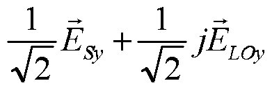 十一信号, 所述第十一信号为 -^ ^+^^ Qy, 第四输出端连接第八 PMOC 的输入端,向第八 PMOC输出第十二信号,所述第十二信号为 ―^^ LOy;
第五衰减器的输出端输出第十三耦合信号, 所述第十三耦合信号为 第七 PMOC的第一输出端输出第十四耦合信号, 所述第十四耦
 合信号为 + _ , 第二输出端输出第十五耦合信号, 所述第十五耦合信 号为 j sy -, 第六衰减器的输出端输出第十六耦合信号, 所述第十六耦
 合信号为 - ^^ + ^«^ 第八 PMOC的第一输出端输出第十七耦合信号, 所 述第十七耦合信号为 Sy 2 LOy , 第二输出端输出第十八耦合信号, 所述第 十八耦合信号为 ;
ESx为双偏振信号在 X偏振方向上的信号, ESy为双偏振信号在 Y偏振方向 上的信号, 为本振在 X偏振方向上的信号, LOy为本振在 Y偏振方向上的 信号。
9、 根据权利要求 8所述的接收机, 其特征在于, 所述信号合并单元包括: 第四 PBC, 第一输入端连接第五 PMOC的第一输出端, 接收第七耦合信号, 第二输入端连接第五衰减器的输出端, 接收第十三耦合信号, 输出端连接第四 PD的输入端, 向第四 PD输出第四合并信号, 所述第四合并信号为所述第七耦 合信号和第十三耦合信号相加;
第五 PBC, 第一输入端连接第五 PMOC的第二输出端, 接收第八耦合信号, 第二输入端连接第七 PMOC的第一输出端, 接收第十四耦合信号, 输出端连接 第五 PD的输入端, 向第五 PD输出第五合并信号, 所述第五合并信号为所述第 八耦合信号和第十四耦合信号相加;
第六 PBC, 第一输入端连接第三衰减器的输出端, 接收第九耦合信号, 第二 输入端连接第七 PMOC的第二输出端, 接收第十五耦合信号, 输出端连接第六 PD的输入端, 向第六 PD输出第六合并信号, 所述第六合并信号为所述第九耦 合信号和第十五耦合信号相加;
第七 PBC, 第一输入端连接第六 PMOC的第一输出端, 接收第十耦合信号, 第二输入端连接第四衰减器的输出端, 接收第十六耦合信号, 输出端连接第七 PD的输入端, 向第七 PD输出第七合并信号, 所述第七合并信号为所述第十耦
合信号和第十六耦合信号相加;
第八 PBC, 第一输入端连接第六 PMOC的第二输出端, 接收第十一耦合信 号, 第二输入端连接第八 PMOC的第一输出端, 接收第十七耦合信号, 输出端 连接第八 PD的输入端, 向第八 PD输出第八合并信号, 所述第八合并信号为所 述第十一耦合信号和第十七耦合信号相加;
第九 PBC, 第一输入端连接第四衰减器的输出端, 接收第十二耦合信号, 第 二输入端连接第八 PMOC的第二输出端, 接收第十八耦合信号, 输出端连接第 九 PD的输入端, 向第九 PD输出第九合并信号, 所述第九合并信号为所述第十 二耦合信号和第十八耦合信号相加;
第四 PD, 输出端输出第四合并信号的电信号;
第五 PD, 输出端输出第五合并信号的电信号;
第六 PD, 输出端输出第六合并信号的电信号;
第七 PD, 输出端输出第七合并信号的电信号;
第八 PD, 输出端输出第八合并信号的电信号;
第九 PD, 输出端输出第九合并信号的电信号。
10、 根据权利要求 9所述的接收机, 其特征在于, 数字信号获取单元包括: 第三转换器, 用于将接收到的合并信号的电信号分别转换成数字信号; 第二处理器, 所述第二处理器连接第二转换器的输出端, 用于将第二转换器 输出的第四合并信号的电信号的数字信号与第五合并信号的电信号的数字信号 相减, 得到双偏振信号在 Y偏振方向上正交分量电信号的数字信号; 将第二转 换器输出的第五合并信号的电信号的数字信号与第六合并信号的电信号的数字 信号相减, 得到双偏振信号在 X偏振方向上正交分量电信号的数字信号; 将第 二转换器输出的第七合并信号的电信号的数字信号与第八合并信号的电信号的 数字信号相减, 得到双偏振信号在 Y偏振方向上同相分量电信号的数字信号; 将第二转换器输出的第八合并信号的电信号的数字信号与第九合并信号的电信 号的数字信号相减, 得到双偏振信号在 X偏振方向上同相分量电信号的数字信 号。
11、根据权利要求 9所述的接收机,其特征在于,所述信号合并单元还用于: 将第四合并信号的电信号与第五合并信号的电信号相减,得到双偏振信号在 Y偏振方向上正交分量的电信号;将第五合并信号的电信号与第六合并信号的电 信号相减, 得到双偏振信号在 X偏振方向上正交分量的电信号;
将第七合并信号的电信号与第八合并信号的电信号相减,得到双偏振信号在
Y偏振方向上同相分量的电信号;将第八合并信号的电信号与第九合并信号的电 信号相减, 得到双偏振信号在 X偏振方向上同相分量的电信号;
所述数字信号获取单元包括:
第四转换器, 用于将双偏振信号在 Υ偏振方向上同相分量的电信号、 双偏 振信号在 X偏振方向上同相分量的电信号、 双偏振信号在 Υ偏振方向上正交分 量的电信号和双偏振信号在 X偏振方向上正交分量的电信号分别转换成数字信 号。
12、 根据权利要求 11所述的接收机, 其特征在于, 所述信号合并单元还具 体包括:
第三减法器,正输入端连接第四 PD的输出端,输入第四合并信号的电信号, 负输入端连接第五 PD的输出端, 输入第五合并信号的电信号, 输出端输出双偏 振信号在 Υ偏振方向上正交分量的电信号;
第四减法器,正输入端连接第五 PD的输出端,输入第五合并信号的电信号, 负输入端连接第六 PD的输出端, 输入第六合并信号的电信号, 输出端输出双偏 振信号在 X偏振方向上正交分量的电信号;
第五减法器,正输入端连接第七 PD的输出端,输入第七合并信号的电信号, 负输入端连接第八 PD的输出端, 输入第八合并信号的电信号, 输出端输出双偏 振信号在 Υ偏振方向上同相分量的电信号;
第六减法器,正输入端连接第八 PD的输出端,输入第八合并信号的电信号, 负输入端连接第九 PD的输出端, 输入第九合并信号的电信号, 输出端输出双偏 振信号在 X偏振方向上同相分量的电信号。
13、 根据权利要求 1至 7任一项所述的接收机, 其特征在于, 还包括: 第三处理器, 用于接收双偏振信号在 X偏振方向上电信号的数字信号以及 双偏振信号在 Υ偏振方向上电信号的数字信号, 通过以下矩阵对所述 X偏振方 向上电信号的数字信号以及 Υ偏振方向上电信号的数字信号进行处理, 得到双 偏振信号的解调结果:

其中, a为信号偏振坐标与 PBS坐标存在的角度差。
14、 一种接收机, 其特征在于, 包括:
信号获取单元,用于接收双偏振信号,对所述双偏振信号进行偏振分束处理, 得到所述双偏振信号分别在 X和 Y偏振方向上的信号;
信号转换单元, 与所述信号获取单元连接, 用于将所述双偏振信号分别在 X 和 Y偏振方向上的信号分别转换为电信号;
数字信号转换单元, 与所述信号转换单元连接, 用于将所述信号转换单元输 出的电信号分别转换成数字信号;
其中,所述双偏振信号中每 3帧数据为一个单元, 3帧数据的结构依次包括: &和 、 和- ^^、 - 和- χ为双偏振信号在 X偏振方向上的信号,
ESy为双偏振信号在 Y偏振方向上的信号。
15、 根据权利要求 14所述的接收机, 其特征在于, 所述信号获取单元包括: 所述第三偏振分束器 PBS的输入端接收双偏振信号, 所述第三 PBS的第一 输出端输出双偏振信号在 X偏振方向上的信号, 所述第三 PBS的第二输出端输 出双偏振信号在 Y偏振方向上的信号。
16、 根据权利要求 15所述的接收机, 其特征在于, 所述信号转换单元包括: 第十光电探测器 PD, 输入端与第三 PBS的第一输出端连接, 接收双偏振信 号在 X偏振方向上的信号, 输出端输出双偏振信号在 X偏振方向上的信号的电 信号;
第十一 PD, 输入端与第三 PBS的第二输出端连接, 接收双偏振信号在 Y偏 振方向上的信号, 输出端输出双偏振信号在 Y偏振方向上的信号的电信号。
17、 根据权利要求 16所述的接收机, 其特征在于, 所述数字信号转换单元 包括:
第十模数转换器 ADC,输入端与第十 PD的输出端连接,将双偏振信号在 X 偏振方向上的信号的电信号转换成数字信号;
第十一 ADC, 输入端与第十一 PD的输出端连接, 将双偏振信号在 Y偏振 方向上的信号的电信号转换成数字信号。
Priority Applications (4)
| Application Number | Priority Date | Filing Date | Title |
|---|---|---|---|
| CN201480070137.2A CN105850051B (zh) | 2014-04-30 | 2014-04-30 | 一种接收机 |
| EP14890562.3A EP3131216B1 (en) | 2014-04-30 | 2014-04-30 | Receiver |
| PCT/CN2014/076643 WO2015165094A1 (zh) | 2014-04-30 | 2014-04-30 | 一种接收机 |
| US15/338,150 US9960856B2 (en) | 2014-04-30 | 2016-10-28 | System and method for optical receiver |
Applications Claiming Priority (1)
| Application Number | Priority Date | Filing Date | Title |
|---|---|---|---|
| PCT/CN2014/076643 WO2015165094A1 (zh) | 2014-04-30 | 2014-04-30 | 一种接收机 |
Related Child Applications (1)
| Application Number | Title | Priority Date | Filing Date |
|---|---|---|---|
| US15/338,150 Continuation US9960856B2 (en) | 2014-04-30 | 2016-10-28 | System and method for optical receiver |
Publications (1)
| Publication Number | Publication Date |
|---|---|
| WO2015165094A1 true WO2015165094A1 (zh) | 2015-11-05 |
Family
ID=54358047
Family Applications (1)
| Application Number | Title | Priority Date | Filing Date |
|---|---|---|---|
| PCT/CN2014/076643 Ceased WO2015165094A1 (zh) | 2014-04-30 | 2014-04-30 | 一种接收机 |
Country Status (4)
| Country | Link |
|---|---|
| US (1) | US9960856B2 (zh) |
| EP (1) | EP3131216B1 (zh) |
| CN (1) | CN105850051B (zh) |
| WO (1) | WO2015165094A1 (zh) |
Families Citing this family (2)
| Publication number | Priority date | Publication date | Assignee | Title |
|---|---|---|---|---|
| WO2015143664A1 (zh) * | 2014-03-27 | 2015-10-01 | 华为技术有限公司 | 监测光性能参数的装置、方法和光传输系统 |
| CN110995349B (zh) * | 2019-11-22 | 2021-01-15 | 中山大学 | 一种基于ddmzm的无ssbi的直接检测方法 |
Citations (4)
| Publication number | Priority date | Publication date | Assignee | Title |
|---|---|---|---|---|
| US20060098986A1 (en) * | 2004-11-10 | 2006-05-11 | Jung Eui S | Optical receiver for reducing optical beat interference and optical network including the optical receiver |
| CN101686096A (zh) * | 2008-09-27 | 2010-03-31 | 华为技术有限公司 | 一种多载波相干接收电处理的方法、装置和系统 |
| CN103257402A (zh) * | 2013-04-23 | 2013-08-21 | 青岛海信宽带多媒体技术有限公司 | 光混合器以及应用光混合器进行信号解调的方法 |
| CN103414680A (zh) * | 2013-08-27 | 2013-11-27 | 北京邮电大学 | 能够消除信号间拍频干扰的平衡光电探测方法和系统 |
Family Cites Families (5)
| Publication number | Priority date | Publication date | Assignee | Title |
|---|---|---|---|---|
| US20100021163A1 (en) * | 2008-07-24 | 2010-01-28 | The University Of Melbourne | Method and system for polarization supported optical transmission |
| US8295713B2 (en) * | 2009-03-10 | 2012-10-23 | Tyco Electronics Subsea Communications Llc | Dual stage carrier phase estimation in a coherent optical signal receiver |
| US9048956B2 (en) * | 2010-11-18 | 2015-06-02 | Nec Corporation | Coherent optical receiver device and coherent optical receiving method |
| US8725006B2 (en) | 2011-02-25 | 2014-05-13 | Nec Laboratories America, Inc. | Digital signal-to-signal beat noise reduction for filter-less coherent receiving system |
| US8584156B2 (en) | 2012-03-29 | 2013-11-12 | Sony Corporation | Method and apparatus for manipulating content channels |
-
2014
- 2014-04-30 CN CN201480070137.2A patent/CN105850051B/zh active Active
- 2014-04-30 EP EP14890562.3A patent/EP3131216B1/en not_active Not-in-force
- 2014-04-30 WO PCT/CN2014/076643 patent/WO2015165094A1/zh not_active Ceased
-
2016
- 2016-10-28 US US15/338,150 patent/US9960856B2/en not_active Expired - Fee Related
Patent Citations (4)
| Publication number | Priority date | Publication date | Assignee | Title |
|---|---|---|---|---|
| US20060098986A1 (en) * | 2004-11-10 | 2006-05-11 | Jung Eui S | Optical receiver for reducing optical beat interference and optical network including the optical receiver |
| CN101686096A (zh) * | 2008-09-27 | 2010-03-31 | 华为技术有限公司 | 一种多载波相干接收电处理的方法、装置和系统 |
| CN103257402A (zh) * | 2013-04-23 | 2013-08-21 | 青岛海信宽带多媒体技术有限公司 | 光混合器以及应用光混合器进行信号解调的方法 |
| CN103414680A (zh) * | 2013-08-27 | 2013-11-27 | 北京邮电大学 | 能够消除信号间拍频干扰的平衡光电探测方法和系统 |
Non-Patent Citations (1)
| Title |
|---|
| See also references of EP3131216A4 * |
Also Published As
| Publication number | Publication date |
|---|---|
| CN105850051B (zh) | 2018-12-07 |
| EP3131216A1 (en) | 2017-02-15 |
| US9960856B2 (en) | 2018-05-01 |
| EP3131216B1 (en) | 2018-10-24 |
| CN105850051A (zh) | 2016-08-10 |
| US20170048002A1 (en) | 2017-02-16 |
| EP3131216A4 (en) | 2017-08-09 |
Similar Documents
| Publication | Publication Date | Title |
|---|---|---|
| US10841014B2 (en) | Optical receiver and coherent optical reception method | |
| JP5527441B2 (ja) | コヒーレント光受信器、コヒーレント光受信方法、コヒーレント光受信器におけるチャネル間スキュー検出装置および検出方法 | |
| CN103475793B (zh) | 使用附加终端进行呼叫 | |
| CN113132020B (zh) | 相干光接收装置和采用相干光接收装置的光系统 | |
| JP2012070051A (ja) | コヒーレント光受信器およびその制御方法 | |
| CN108768540B (zh) | 光信号接收装置、方法及具有该装置的相干光传输系统 | |
| WO2014146236A1 (zh) | 相干光通信的装置和方法 | |
| US8849130B2 (en) | Coherent optical receivers for colorless reception | |
| CN112291018B (zh) | 一种相干接收机的光电接收装置、接收方法及相干接收机 | |
| WO2012103832A2 (zh) | 信号处理方法、光接收机以及光网络系统 | |
| WO2020211390A1 (zh) | 一种相干光学接收装置及光信号解调装置 | |
| CN102546026B (zh) | 一种相干光接收机输出信号的偏斜检测方法和系统 | |
| CN104125654A (zh) | 一种wifi网络的数据传输方法、装置及终端设备 | |
| WO2012117951A1 (ja) | 光受信器および光受信方法 | |
| CN105850051B (zh) | 一种接收机 | |
| CN104145432A (zh) | 接收器、传输系统、用于接收偏振复用光学信号的方法,以及存储接收器控制程序的非瞬态计算机可读介质 | |
| CN103051375A (zh) | 无线激光通信外差检测系统及其检测方法 | |
| WO2012106882A1 (zh) | 去延时方法、装置和光通信系统接收器 | |
| CN111698027A (zh) | 一种相干检测方法及相干接收机 | |
| US10254556B2 (en) | Polarization rotator-combiner for optical communications | |
| CN107925483B (zh) | 光信号处理方法及相干接收机 | |
| JP2021061508A (ja) | 光受信装置 | |
| CN115102627A (zh) | 基于差分调制的光纤传输接收端和光纤通信系统 | |
| Kim et al. | VCSEL-based coherent detection of 10-Gbit/s QPSK signals using digital phase noise cancellation for future optical access systems | |
| CN222868928U (zh) | 一种无光滤波器的扩展带宽外差相干接收机构 |
Legal Events
| Date | Code | Title | Description |
|---|---|---|---|
| 121 | Ep: the epo has been informed by wipo that ep was designated in this application |
Ref document number: 14890562 Country of ref document: EP Kind code of ref document: A1 |
|
| NENP | Non-entry into the national phase |
Ref country code: DE |
|
| REEP | Request for entry into the european phase |
Ref document number: 2014890562 Country of ref document: EP |
|
| WWE | Wipo information: entry into national phase |
Ref document number: 2014890562 Country of ref document: EP |