WO2015173850A1 - ワイヤレス電力伝送装置 - Google Patents
ワイヤレス電力伝送装置 Download PDFInfo
- Publication number
- WO2015173850A1 WO2015173850A1 PCT/JP2014/004827 JP2014004827W WO2015173850A1 WO 2015173850 A1 WO2015173850 A1 WO 2015173850A1 JP 2014004827 W JP2014004827 W JP 2014004827W WO 2015173850 A1 WO2015173850 A1 WO 2015173850A1
- Authority
- WO
- WIPO (PCT)
- Prior art keywords
- coil
- secondary coil
- phase
- primary coil
- resonance
- Prior art date
- Legal status (The legal status is an assumption and is not a legal conclusion. Google has not performed a legal analysis and makes no representation as to the accuracy of the status listed.)
- Ceased
Links
Images


Classifications
-
- H—ELECTRICITY
- H02—GENERATION; CONVERSION OR DISTRIBUTION OF ELECTRIC POWER
- H02J—ELECTRIC POWER NETWORKS; CIRCUIT ARRANGEMENTS OR SYSTEMS FOR SUPPLYING OR DISTRIBUTING ELECTRIC POWER; SYSTEMS FOR STORING ELECTRIC ENERGY
- H02J50/00—Circuit arrangements or systems for wireless supply or distribution of electric power
- H02J50/10—Circuit arrangements or systems for wireless supply or distribution of electric power using inductive coupling
- H02J50/12—Circuit arrangements or systems for wireless supply or distribution of electric power using inductive coupling of the resonant type
-
- G—PHYSICS
- G01—MEASURING; TESTING
- G01R—MEASURING ELECTRIC VARIABLES; MEASURING MAGNETIC VARIABLES
- G01R25/00—Arrangements for measuring phase angle between a voltage and a current or between voltages or currents
- G01R25/005—Circuits for comparing several input signals and for indicating the result of this comparison, e.g. equal, different, greater, smaller, or for passing one of the input signals as output signal
-
- H—ELECTRICITY
- H02—GENERATION; CONVERSION OR DISTRIBUTION OF ELECTRIC POWER
- H02J—ELECTRIC POWER NETWORKS; CIRCUIT ARRANGEMENTS OR SYSTEMS FOR SUPPLYING OR DISTRIBUTING ELECTRIC POWER; SYSTEMS FOR STORING ELECTRIC ENERGY
- H02J50/00—Circuit arrangements or systems for wireless supply or distribution of electric power
- H02J50/80—Circuit arrangements or systems for wireless supply or distribution of electric power involving the exchange of data, concerning supply or distribution of electric power, between transmitting devices and receiving devices
Definitions
- the present invention relates to a wireless power transmission device, and in particular, a primary coil connected to a high-frequency power source and a secondary coil connected to a load are arranged with a coupling coefficient k spaced apart from the primary coil to the secondary coil.
- the present invention relates to a wireless power transmission device in which power is supplied by contact.
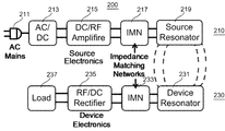
- FIG. 24 is a block diagram showing a configuration of a conventional magnetic field resonance type wireless power transmission device, and FIG. 25 shows an equivalent circuit diagram thereof.
- the wireless power transmission apparatus 200 includes a primary side circuit (Source Electronics) 210 and a secondary side circuit (Device Electronics) 230.
- the primary side circuit 210 converts an alternating current supplied from an alternating current (AC) power source (AC mains) 211 into a direct current, and converts the direct current (DC) into a predetermined high frequency (RF).
- a high frequency driving circuit 215 that amplifies and outputs, a primary side resonator (Source ⁇ ⁇ ⁇ Resonator) 219 to which this high frequency is supplied as driving power, and an impedance matching circuit (Impedance) that performs impedance matching between the primary side resonator 219 Matching Networks) 217.
- the secondary side circuit 230 converts an RF / DC rectifier circuit (RF / DC) that converts a secondary side resonator (Device Resonator) 231, an impedance matching circuit (IMN) 233, and a high frequency (RF) into direct current, rectifies and outputs the direct current.
- Rectifier 235 and a load 237 to which rectified DC power is supplied.
- the primary side resonator 219 includes a primary coil and a primary resonance capacitor
- the secondary side resonator 230 includes a secondary coil and a secondary resonance capacitor.
- the resonance frequencies of the primary resonator 219 and the secondary resonator 231 are matched, and both resonators are made to resonate with each other. It is said that efficient power transmission is realized.
- the respective resonators 219 and 231 are controlled by matching impedance conditions using impedance matching circuits (IMN) 217 and 233, respectively.
- INN impedance matching circuits
- Vg, Rg, Cs, Ls, and Rs of the primary side circuit 210 are respectively a high frequency driving voltage, an equivalent resistance of the high frequency driving circuit, a capacitance of the resonant capacitor, a self inductance of the primary coil, and a primary coil.
- RL, Cd, Ld, and Rd of the secondary side circuit indicate the equivalent resistance of the load, the capacitance of the resonant capacitor, the self-inductance of the secondary coil, and the equivalent resistance of the secondary coil, respectively.
- M represents the mutual inductance between the primary coil and the secondary coil.
- it is essential to include a primary-side resonator 219 shown in FIG. 24, which is the greatest feature of the magnetic field resonance method.
- the primary resonant capacitor Cs is an essential component.
- the coupling coefficient k of the leakage flux transformer composed of the primary coil and the secondary coil changes, and the load also changes at the same time.
- wireless power transmission has many magnetic parameters that change when focusing on the electronic circuits that make up the wireless power transmission. Therefore, it can be said that it is very difficult to simultaneously achieve high efficiency, stability, reliability, and the like.
- ZVS Zero Voltage Switching
- the primary side resonance frequency is constant regardless of the distance between the coils, but the secondary side resonance frequency is between the coils. And the resonance frequency also changes when the coupling coefficient changes.
- the inductance of the secondary coil and L 2 a resonant capacitor and Cp, if the coupling coefficient is k,
- the resonance frequencies of the primary side and the secondary side match only when the distance between the coils is a predetermined distance, and the resonance frequencies do not match at other distances between the coils. Become.
- the phase relationship between the primary coil and the secondary coil must be within a specific range, and only under very limited conditions.
- the ZVS operation is not performed. Therefore, in the conventional wireless power transmission, in order to constantly ensure the ZVS operation, measures are taken such as changing the drive frequency according to a certain program while observing the state of the load.
- An object of the present invention is to solve some of the above-described various problems associated with the conventional magnetic field resonance method.
- An object of the present invention is to provide a wireless power transmission device that can maintain and realize efficient power transmission.
- a simple circuit reduces both copper loss and switching loss, and the wireless power transmission device is highly robust and highly efficient. The purpose is to provide.
- the primary coil connected to the high-frequency power source and the secondary coil connected to the load are arranged separated by a coupling coefficient k, and the primary coil is not contacted with the secondary coil.
- the wireless power transmission device for supplying power at a resonance current phase detecting means for detecting a phase information of a resonance current flowing in the resonance capacitor by configuring a resonance circuit by coupling a resonance capacitor to the secondary coil, And phase information transmission means for transmitting the phase information without phase delay, and based on the phase information, the current phase of the drive current flowing through the primary coil is slightly delayed from the voltage phase of the drive voltage applied to the primary coil.
- the primary coil connected to the high-frequency power source and the secondary coil connected to the load are arranged separated by a coupling coefficient k, and the primary coil is not contacted with the secondary coil.
- the wireless power transmission device for supplying power at a resonance current phase detection means for detecting a phase information of a resonance current flowing in the secondary coil by configuring a resonance circuit by coupling a resonance capacitor to the secondary coil, and detection Phase information transmission means for transmitting the phase information without phase delay, and based on the phase information
- the current phase of the drive current flowing through the primary coil is slightly smaller than the voltage phase of the drive voltage applied to the primary coil
- the primary coil connected to the high-frequency power source and the secondary coil connected to the load are arranged separated by a coupling coefficient k, and the primary coil is not contacted with the secondary coil.
- the wireless power transmission apparatus for supplying power at a resonance current phase detection means for detecting a phase information of a resonance current flowing in the resonance circuit from the primary coil by configuring a resonance circuit by coupling a resonance capacitor to the secondary coil
- phase information transmission means for transmitting the detected phase information without phase delay, and based on the phase information
- the current phase of the drive current flowing through the primary coil is the voltage phase of the drive voltage applied to the primary coil
- the primary coil connected to the high-frequency power source and the secondary coil connected to the load are arranged separated by a coupling coefficient k, and the primary coil is not contacted with the secondary coil.
- a resonance capacitor is coupled to the secondary coil to form a resonance circuit, and a waveform of the resonance current that flows through the resonance capacitor, A resonance current for detecting phase information of the resonance current based on a waveform obtained by superimposing and combining one of the waveforms of the resonance current flowing through the primary coil and a waveform obtained by inverting and integrating any of the waveforms.
- a phase detection unit ; a phase information transmission unit configured to transmit the detected phase information without phase delay; and a current phase of a drive current flowing through the primary coil based on the phase information.
- a drive circuit for driving the primary coil by setting a drive frequency so as to be slightly delayed from a voltage phase of a drive voltage applied to the coil, and a leakage inductance of the secondary coil, a capacitance of the resonant capacitor, and the second
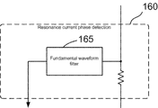
- a filter that removes distortion contained in the waveform of the resonance current and extracts only the fundamental wave is provided.
- the drive circuit includes a switching unit that drives the primary coil, and the switching unit varies an ON-OFF duty ratio, Based on the phase information, the switching means is turned on, and the power is controlled by turning off the switching means after a certain time.
- the resonance current phase detection means detects the phase information from a current flowing through a small-capacitance capacitor connected in parallel to the resonance capacitor. Yes.
- a primary coil connected to a high-frequency power source, a secondary coil connected to a load, a proximity of the secondary coil, or including the secondary coil as an autotransformer,
- a third coil wound in a step-down relationship with respect to the voltage induced in the secondary coil, the primary coil and the secondary coil are spaced apart by a coupling coefficient k, and the primary coil is separated from the primary coil.
- a resonance capacitor is coupled to the secondary coil to form a resonance circuit, and the resonance current flowing through the resonance capacitor
- Resonance current phase detection means for detecting phase information, phase information transmission means for transmitting the detected phase information without phase delay, and a drive current flowing in the primary coil based on the phase information
- a drive circuit for driving the primary coil by setting a drive frequency so that a current phase is slightly delayed from a voltage phase of a drive voltage applied to the primary coil, and a leakage inductance of the secondary coil and the resonant capacitor
- a primary coil connected to a high frequency power supply, a secondary coil connected to a load, and the secondary coil are close to each other, or the secondary coil is an autotransformer, and the secondary coil
- a third coil wound in a step-down relationship with respect to the voltage induced in the secondary coil is included in the autotransformer, and the primary coil and the secondary coil are separated by a coupling coefficient k.
- a resonance capacitor is coupled to the secondary coil to form a resonance circuit, and a resonance current that flows through the secondary coil
- Resonant current phase detection means for detecting phase information of the current
- phase information transmission means for transmitting the detected phase information without phase delay
- drive that flows to the primary coil based on the phase information
- a primary coil connected to a high frequency power supply, a secondary coil connected to a load, and the secondary coil are close to each other, or the secondary coil is an autotransformer, and the secondary coil
- a third coil wound in a step-down relationship with respect to the voltage induced in the secondary coil is included in the autotransformer, and the primary coil and the secondary coil are separated by a coupling coefficient k.
- a resonance capacitor is coupled to the secondary coil to form a resonance circuit, and the resonance current flowing through the resonance circuit
- Resonance current phase detection means for detecting phase information from the primary coil, phase information transmission means for transmitting the detected phase information without phase delay, and based on the phase information
- the primary A drive circuit for driving the primary coil by setting a drive frequency so that a current phase of a drive current flowing through the coil is slightly delayed from a voltage phase of a drive voltage applied to the primary coil,
- a primary coil connected to a high-frequency power source, a secondary coil connected to a load, and the secondary coil are close to each other, or the secondary coil is an autotransformer,
- a third coil wound in a step-down relationship with respect to the voltage induced in the secondary coil is included in the autotransformer, and the primary coil and the secondary coil are separated by a coupling coefficient k.
- a resonance capacitor is coupled to the secondary coil to form a resonance circuit, and the resonance current flowing through the resonance capacitor A waveform, a waveform of a resonance current flowing through the secondary coil, or a waveform of a resonance current flowing through the primary coil, and a waveform obtained by inverting and integrating any of the waveforms
- a resonance current phase detection means for detecting phase information of the resonance current based on a waveform obtained by tatami synthesis
- a phase information transmission means for transmitting the detected phase information without phase delay
- a drive circuit for driving the primary coil by setting a drive frequency so that a current phase of a drive current flowing through the primary coil is slightly delayed from a voltage phase of a drive voltage applied to the primary coil, and
- the Q value determined by the leakage inductance of the secondary coil, the resonant capacitor, and the equivalent load resistance on the secondary coil side is set to a value
- a filter that removes distortion contained in the waveform of the resonance current and extracts only the fundamental wave is provided.
- the drive circuit includes a switching unit that drives the primary coil, and the switching unit varies an ON-OFF duty ratio, Based on the phase information, the switching means is turned on, and the power is controlled by turning off the switching means after a certain time.
- the resonance current phase detection means detects the phase information from a current flowing through a small-capacitance capacitor connected in parallel to the resonance capacitor. Yes.
- the resonance circuit is provided by connecting the resonance capacitor only to the secondary coil without providing the resonance circuit in the primary coil, the resonance current does not flow through the primary coil, so that heat generation in the primary coil is suppressed.
- the frequency having the best power factor seen from the primary coil side can be automatically selected as the drive frequency, so that the robustness is greatly improved.
- a half-bridge circuit configuration can be adopted as the drive circuit, and the device can be realized with a simpler circuit configuration than a conventional wireless power transmission device.
- the block diagram which shows the structure of the principal part of the wireless power transmission apparatus which concerns on this invention.
- the circuit diagram which shows an example of the switching means used for this invention.
- the figure which shows the structure of the detection part containing the resonance current phase detection means of this invention.
- the figure showing the other example of the resonance current phase detection means of this invention.
- the figure showing the further another example of the resonance current phase detection means of this invention.
- the figure explaining that phase information goes wrong by the distortion contained in a resonance current phase waveform.
- the conceptual diagram which shows removing a harmonic distortion from a resonance current phase waveform.
- the conceptual diagram which shows the change of the various waveforms when a phase delay arises in resonance current phase information.
- FIG. 6 is still another specific circuit diagram when performing phase correction.
- FIG. 1 is a block diagram showing a configuration of a main part of one embodiment of a wireless power transmission apparatus 100 according to the present invention.
- the primary side includes a driving circuit 120 connected to a primary coil 110 via a capacitor Cc.
- the driving circuit 120 includes a driving means 122 and a switching means 124. It is configured.
- the switching means 124 is configured as a bridge circuit including transistor elements Q1 to Q4.
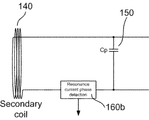
- the secondary side includes a secondary coil 140 that is spaced apart from the primary coil 110 by a coupling coefficient k, and a resonance capacitor (Cp) 150 that is coupled to the secondary coil 140 to form a resonance circuit.
- Resonance current phase detection means 160 for detecting phase information of the resonance current flowing through the resonance capacitor (Cp) 150.
- the present invention includes phase information transmission means 170 that transmits phase information detected by the resonance current phase detection means 160 to the drive circuit 120 without phase delay, and the drive circuit 120 determines a drive frequency based on this phase information.
- the phase information transmission unit 170 includes a phase information transmitter 172 and a phase information receiver 174.
- the secondary side is connected to a load (not shown).
- the resonance circuit is only a resonance circuit configured by coupling the resonance capacitor (Cp) 150 to the secondary coil 140, and no positive series resonance capacitor is provided in the primary coil 110.
- the capacitor Cc shown in FIG. 1 is provided only for the purpose of blocking direct current, and is not provided as a resonant capacitor. More specifically, when the capacitance of this capacitor is set to be small in consideration of cost and the like, it may be slightly involved in the resonance on the primary side, but this is not an essential resonance. Further, the capacitor Cc can be omitted if the drive timing of the switching means 124 can be precisely controlled and the balance of the currents flowing through the transistor elements Q1 to Q4 can be maintained.
- the phase information of the resonance current flowing in the resonance circuit composed of the secondary coil 140 and the resonance capacitor (Cp) 150 connected in parallel or in series is detected by the resonance current phase detection means 160, and the phase is detected.
- Information is sent from the phase information transmitting means 172 on the secondary side to the phase information receiving means 174 on the primary side, and the driving timing of the driving means 122 is determined based on the phase information.
- the resonance circuit since the resonance circuit is not provided on the primary side, the number of turns of the primary coil 110 is different from that of the conventional magnetic field resonance method that requires the primary side resonance circuit.
- the phase information transmission unit 170 transmits the phase information detected by the resonance current phase detection unit 160 "without phase delay", but any detection unit or transmission unit necessarily has a phase delay. Therefore, here, “without phase delay” means to make the phase delay as small as possible, and it is sufficient that the primary side driving means and the secondary side can share the absolute time for the purpose.
- the driving unit 122 Based on the phase information transmitted from the phase information transmitting unit 170, the driving unit 122 is configured so that the current phase of the driving current flowing through the primary coil 110 is slightly delayed from the voltage phase of the driving voltage applied to the primary coil 110.
- the drive frequency is determined and the switching means 124 is driven.
- the switching means 124 is composed of switching elements (Q1 to Q4) such as 2 or 4 transistors, and drives the primary coil 110 via a DC blocking capacitor Cc.
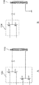
- FIG. 2 is a circuit diagram showing an example of the switching means 124, in which A indicates a full bridge circuit and B indicates a half bridge circuit.
- the switching means 124 may be a full bridge circuit or a half bridge circuit.
- the phase relationship between the driving voltage applied to the primary coil 110 and the driving current flowing through the primary coil 110 as viewed from the switching means 124 side greatly varies depending on the driving frequency. It was difficult to keep hard and prevent hard switching. Therefore, a full bridge circuit has been favorably used because abnormal voltages are unlikely to occur even when hard switching occurs.
- a half-bridge circuit which is said to be difficult due to hard switching, can be employed with peace of mind. This is because in the present invention, ZVS can be maintained under various conditions. Details will be described later.
- the full bridge circuit has only the advantage that the utilization efficiency of the power supply is high, and is not an essential condition in the present invention. Therefore, a case where a full bridge circuit is used as the switching means 124 will be described below.
- FIG. 3 is a diagram showing a configuration of a detection unit including the resonance current phase detection means 160 of the present invention.
- a resonant capacitor (Cp) 150 and a small-capacitance capacitor (Cps) 155 are connected to the secondary coil 140 in parallel.
- the resonance current detection means 160 may detect the phase information of the current flowing directly through the resonance capacitor (Cp) 150 as shown in FIG. 1, or may be a small size connected in parallel as shown in FIG. It may be one (160a) that detects phase information of the current flowing through the capacitor (Cps) 155.
- the resonance current detection means 160 must be composed of a large capacity component. If the current flowing in (Cps) is detected, it can be constituted by a small capacity component.
- the phase information of the resonance current detected by the resonance current phase detection unit 160 is transmitted to the drive circuit 120 on the primary side by the resonance current phase transmission unit 170.
- the resonance current phase transmission means 170 are conceivable, but optical coupling using an LED and a phototransistor may be used, and the magnetic circuit is modulated and transmitted by a signal obtained by digitizing phase information.
- a wireless means using an electromagnetic wave of a high frequency carrier may be used.
- a phototransistor is used as the light receiving portion, the delay due to the accumulated charge is large, and means for saturating the phototransistor is not preferable.
- the phototransistor preferably has a non-saturated operation, and more preferably has a constant voltage operation for suppressing the mirror effect. It is more preferable to use a Pin photodiode or to use it with a reverse bias to achieve high-speed operation.
- the resonance current phase detection means 160 may be one (160b) that detects a current flowing through the secondary coil 140 as shown in FIG. In this case, however, the detected phase information is combined with the phase component of the current flowing through the load. Since the phase component of the current flowing through the load is delayed by 90 ° from the resonance current phase, these vectors are combined to cause a slight phase delay in the phase information.
- the primary coil 110 is driven based on this phase information, the ZVS operation is lost and hard switching is likely to occur.
- hard switching occurs, high-frequency parasitic vibrations occur in the elements (Q1 to Q4) of the switching means 124.
- EMI Electro-Magnetic Interference
- noise power / noise electric field strength (radiation) Will increase. Therefore, countermeasures are required, which will be described later.
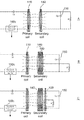
- the resonance current phase detection means 160 may be one (160c) that detects the current flowing through the primary coil 110 as shown in FIG.
- A is a type in which power is extracted from the secondary coil 140 to the load R
- B is a type in which the secondary coil includes a third coil 190 as an autotransformer, and power is extracted from the third coil 190 to the load R.
- Each of the types is shown in which power is extracted from a third coil 190 provided as an independent coil close to the next coil 140 to a load R.
- the details of the types B and C in which the third coil 190 is provided on the secondary side will be described later. In these cases, since hard switching occurs in many cases, it is necessary to separately correct the phase, which will be described later.
- the detected resonance current is distorted as a cause of delay of the resonance current phase information.
- Such distortion causes the resonance current phase information to be distorted, the drive timing of the primary coil 110 becomes inaccurate, and the peak of the resonance frequency cannot be detected correctly.
- FIG. 6 is an example of a case where the resonant current includes a third-order high frequency, and is an explanatory diagram for explaining that the phase information is distorted due to this distortion.
- the phase information it is possible to improve the accuracy of the phase information by taking out only the basic component by using an appropriate filter means and using it as the resonance current phase information.
- FIG. 7 is a conceptual diagram showing that the resonance current phase detection means 160 is provided with a filter (Fundamental wave filter) 165 for extracting only the fundamental wave to remove harmonic distortion from the resonance current phase waveform.
- a filter Frundamental wave filter
- Wireless power transmission is very different from power feeding by a general leakage transformer.
- the coupling coefficient (k) between the primary coil and the secondary coil is substantially constant in all driving conditions, whereas the coupling coefficient (k) varies greatly in wireless power transmission.
- the Q value of the secondary side resonance circuit does not need to be so high.
- the coupling coefficient (k) changes in the case of wireless power transmission, a high Q value is required when the coupling coefficient (k) is small.
- the phase delay (or time delay) in the means for transmitting the resonance current phase information must be minimized.
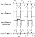
- FIG. 8 is a conceptual diagram showing changes in various waveforms when a phase delay occurs in the resonance current phase information.
- a is the waveform of the resonance current of the resonance circuit
- b is the waveform of the phase information detected by the resonance current phase detection means 160
- c is the waveform of the phase information output from the phase information reception means 174
- d is flowing through the primary coil 11. It is a current waveform of current.
- the waveform c output from the phase information receiving unit 174 is delayed from the waveform b and almost becomes the driving waveform of the switching unit 124 as it is.
- FIG. 9 is a diagram showing a waveform of a current flowing through the switching means 124 when the ZVS operation is performed when the phase delay of the resonance current phase information is small.
- the waveform of the phase information receiving unit 174 has no delay or is extremely small (c)
- the timing of the current flowing through the primary coil 110 is slightly earlier than the switching timing of the switching unit 124 (d )
- the current waveforms (e, f) of the switching elements Q1, Q2 of the switching means 124 are ZVS operations.
- the center tap voltage of the switching means 124 is a clean square wave (g).
- FIG. 10 is a diagram showing a waveform of a current flowing through the switching means 124 when the ZVS operation is not performed when the phase delay of the resonance current phase information is large.
- the timing of the current flowing through the primary coil 110 is delayed (d), so that the current waveforms (e, f) of the switching elements Q1, Q2 do not perform the ZVS operation, and the switching means 124
- a characteristic pulse waveform due to rebound occurs in the center tap voltage of (g).
- the switching elements Q1 and Q2 and the driving means 122 may be destroyed, or EMI may be generated.
- the phase delay in the phase information transmission means 170 must be minimized. If phase delay is unavoidable, the following phase correction means is used.
- FIG. 11 is a diagram illustrating an example of a circuit for correcting the phase of the resonance current phase information.
- An adder circuit 166 that superimposes and synthesizes the output from the circuit 164 is provided.
- the inverted and integrated waveform is 90 degrees ahead of the original resonant current waveform.
- the phase of the resonance current is advanced by detecting the phase information of the resonance current based on the waveform obtained by superimposing the waveform of the original resonance current and the waveform obtained by inverting and integrating the waveform at an appropriate ratio. Corrected resonance current phase information can be obtained. Then, this is sent to the phase information receiving means 174 via the phase information transmitting means 170.
- the inverting integration circuit 164 can be configured using an operational amplifier (op-amp), or can be configured to integrate using a capacitor (C) and a resistor (R) after being inverted using a transformer. .
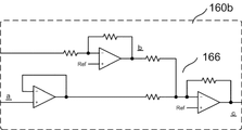
- FIG. 13 is a diagram showing a specific circuit diagram of the resonance current phase detection means 160a when performing phase correction.
- the resonance current waveform information a is inverted and integrated by the inverting integration circuit 164 via the buffer amplifier, and is synthesized by the synthesis circuit 166, whereby the phase advances and a corrected waveform c is obtained (see FIG. 12A).
- FIG. 14 is a diagram showing another specific circuit diagram of the resonance current phase detection means 160b. Focusing on the fact that the voltage across the resonance capacitor Cp150 is an integral waveform with respect to the resonance current waveform, this can be divided appropriately.
- the phase correction is performed by reversing the pressure.
- the resonance current waveform information a is combined with the inverted resonance capacitor voltage by the combining circuit 166, so that the phase advances and a corrected waveform c is obtained (see FIG. 12B).
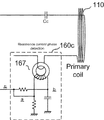
- FIG. 15 is a diagram showing still another specific circuit diagram of the resonance current phase detection means 160c.
- the phase correction is performed by synthesizing the resonance current waveform detected from the primary coil 110 via the current transformer 167 and its inverted integral waveform.
- the resonance current phase waveform detected on the primary side is a
- the inversion-integrated resonance current phase waveform is b
- a corrected waveform c is obtained.
- a differential waveform instead of integration without inversion, and this is included in the meaning of inversion integration as an appropriate design matter in the present invention.
- the harmonic waveform is emphasized and superimposed on the differential waveform, which is not preferable as compared with the case where the integrated waveform is used.
- the phase correction means may further appropriately combine each of the resonance current phase waveforms a of 160a, 160b, and 160c and its inverted integrated waveform b, or replace the circuits of the current detection means 160a and 160b. Also good.
- the phase correction means in the present invention only needs to obtain a correction waveform having a phase advance based on the waveform including the resonance current phase information. If sharing of absolute time can be obtained by some means, it is also possible to obtain corrected phase waveform by obtaining corrected phase information from the difference from the absolute time. That is, it goes without saying that digital processing can be performed based on these findings.
- the coupling coefficient (k) changes. Therefore, when the coupling coefficient (k) is low, a particularly large Q value is required for the resonance circuit.
- the primary coil satisfies the condition that the current phase of the drive current flowing through the primary coil is slightly delayed from the voltage phase of the drive voltage applied to the primary coil. Is difficult to drive.
- the drive frequency is fixed (so-called a fixed frequency method or a separate excitation method).
- the resonance current flowing in the resonance capacitor of the secondary side resonance circuit, the resonance current flowing in the secondary coil Alternatively, it is essential to control the drive circuit based on the phase information of the resonance current reflected in the primary coil. As a result, the drive frequency must be variable.
- Patent Document 1 discloses that the driving frequency is changed according to the resistance component of the load in the wireless power transmission of the magnetic field resonance method.
- the driving means is driven by obtaining the optimum driving frequency by pre-programmed prediction information or calculation and saturable inductor by detecting the load resistance.
- the power factor seen from the switching means of the drive circuit for driving the primary coil since the power factor seen from the switching means of the drive circuit for driving the primary coil only approaches 1, and the power factor seen from the primary coil does not approach 1, the heat generation of the switching means is suppressed.
- the power factor seen from the side of the primary coil is very bad, causing the primary coil to generate heat.
- the setting of the Q value of the resonance circuit on the secondary coil side is set higher than usual.
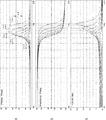
- FIG. 16 is a diagram for explaining the relationship between the current phase of the resonant capacitor coupled to the secondary coil and the current phase of the primary coil.
- the Q value required when the coupling coefficient (k) is changed is obtained by simulation. It is a thing.
- a is the current phase of the primary coil, the vertical axis is the phase angle, and the horizontal axis is the drive frequency.
- b is the current phase of the secondary resonance capacitor, the vertical axis is the phase angle, and the horizontal axis is the drive frequency.
- c is the transmission ratio, the vertical axis is the transmission ratio, and the horizontal axis is the drive frequency. If the transmission ratio is multiplied by the ratio between the number of turns of the primary coil and the number of turns of the secondary coil, the transmission ratio is approximately the boost ratio.
- the coupling coefficient (k) When the coupling coefficient (k) is 0.5, the condition that the phase of the current flowing in the primary coil is slightly delayed from the phase of the drive voltage of the drive circuit that drives the primary coil by setting the Q value to 8 or more. You can see that it meets.
- the frequency at which the transmission ratio is highest is 85 kHz.
- the delay angle ⁇ of the current flowing through the primary coil is 25 deg. Or less, and cos ⁇ , that is, the power factor is 0.9 or more, so 85 kHz can be said to be the optimum driving frequency.
- the phase of the resonant current flowing through the secondary side resonant capacitor is 0 deg. That is, if this resonance current phase information is transmitted to the drive circuit through the phase information transmission means without phase delay and the drive circuit is driven, the switching means can be automatically driven at the optimum drive frequency. Further, since this switching condition is also a ZVS operation, a stable ZVS operation is possible even if the switching means is a half-bridge configuration.
- the drive circuit is driven at the drive frequency determined based on the phase information of the resonance current, and the ZVS operation is automatically performed.
- the ZVS operation is not performed, and phase correction is necessary.
- the Q value of the resonance circuit is determined as follows by the leakage inductance (L) of the secondary coil, the capacitance (C) of the resonance capacitor, and the equivalent load resistance (R) on the secondary coil side.
- both the series connection and the parallel connection can be used for the connection between the secondary coil and the resonant capacitor.
- an example of the parallel connection will be described.
- a resonance circuit in which a resonance capacitor is provided in parallel with a secondary coil which is one of the present invention, is a series of resonant resonances when viewed from the drive side and a parallel resonance when viewed from the load side. That's why. This is called Serial Parallel-Loaded Resonance and various other names. In this case, parallel resonance is applied to the calculation formula of Q.
- the capacitance C of the resonance capacitor is made larger than the equivalent load resistance R, and the leakage inductance L of the secondary coil is made smaller.
- the definition of the leakage inductance L sc in the present invention is determined by the following equation.
- L 2 is the secondary coil inductance or the inductance of the independent third coil.
- Le is defined as a leakage inductance, which is not uniform.
- the resonance circuit configured on the secondary side by coupling the secondary coil and the resonance capacitor is either one in which the resonance capacitor is connected in parallel or in series to the secondary coil. Is included.
- the structure which takes out the electric power connected to a load from a 3rd coil is mentioned later.
- FIG. 17 is a diagram in which the minimum necessary Q value necessary for obtaining the power factor as seen from the primary coil is obtained by simulation.
- the horizontal axis is the drive frequency.
- a indicates the current phase of the primary coil with respect to the switching voltage of the primary coil
- b indicates the resonance current phase of the secondary side resonance capacitor
- c indicates the transmission ratio (transmission coefficient).
- the value of k 2 ⁇ Q gradually approaches 2 and does not exceed 2 as k decreases. This is because, in the wireless power transmission, when the distance between the primary coil and the secondary coil is large and the coupling coefficient k is sufficiently small, the secondary side resonance circuit for obtaining the power factor of 1 when viewed from the primary coil is used.
- Q value is
- the current phase curve of the primary coil must always cross the horizontal axis of 0 deg.
- the phase must cross so that it is positive, that is, capacitive to negative, that is, inductive.
- FIG. 20 is a diagram illustrating an example of power control according to the present invention.
- a is the phase information of the resonance current
- b is the current waveform of the primary coil
- c and d are the gate control voltages when the switching means (Q2, Q1) are FETs, IGBTs or the like.
- the power control in the present invention is performed by turning on the switching means of the drive circuit for driving the primary coil and turning it off after a certain time based on the phase information of the resonance current.
- hard switching is generally a concern.
- the current phase of the primary coil is already behind the switching phase (see b). Since the phase is further delayed than the ON phase (see c and d), hard switching does not occur. At that time, since it is generally performed that a slight dead time (Dead time) is required so that (Q2, Q1) are not simultaneously turned ON, this is omitted in this description.
- FIG. 21 is a diagram illustrating another example of power control according to the present invention.
- the duty control side is only one of the switching means or one of the pair that is simultaneously turned on, and the other or the other pair is controlled by an inversion signal. At that time, a slight dead time is required on the side controlled by the inverted signal (see d).
- Such a control method is called non-uniform half-bridge or non-uniform full-bridge control. In this control method, even-order harmonic voltages are likely to be generated in the secondary coil.
- the Q value is set very high, there is no problem because the voltage of the secondary coil is almost close to a sine wave.
- FIG. 22 is a diagram for explaining the relationship with the current phase of the primary coil when the power control of the present invention is performed.
- the drive frequency when the control is performed is also increased.
- the ON phase of the drive voltage is further delayed than the phase of the phase information of the resonance current.
- the power factor is lowered, but at the same time, the transmission ratio is lowered, so that the controllable power range becomes very wide.
- a resonance circuit is configured by coupling a resonance capacitor to a secondary coil.
- the secondary side resonance circuit as in the present invention is used. Is not required. Therefore, in order to apply the present invention while adopting compatibility with the Qi standard, a third coil is provided in parallel with the secondary coil as shown in FIG. 5C, and electric power connected to the load is taken out from the third coil. The case will be described.
- FIG. 23 is a diagram showing an example of a circuit that can improve efficiency while maintaining compatibility with the Qi standard.
- the third coil 190 may be provided as an independent coil close to the secondary coil 140 as shown in FIG. 5C. However, as shown in FIG. 23 and FIG. A coil may be included, and the third coil 190 may be wound by being wound so as to step down the voltage induced in the secondary coil 140.
- Resonant capacitor (Cp) 150 is coupled to secondary coil 140, and is turned off by switch 181 in the case of the Qi compatible standard, and turned on to improve efficiency, and Cp operates as resonant capacitor 150.
- the switch 183 on the secondary coil 140 side is turned off and the switch 185 is turned on.
- a load (not shown) is connected between the switch 183 and the switch 185 between the secondary side GND.
- the resonance current waveform detected by the resonance current phase detection means 160c provided on the primary side and its inverted integral waveform are combined to produce a phase. Correction may be performed and the driving circuit of the high frequency power source may be driven based on the resonance current phase information.
- the switches 181, 183, and 185 use FETs or transistors via diodes. However, any element can be used as long as it is an element capable of switching operation.
- the load resistance connected to the third coil is Since impedance conversion is performed in inverse proportion to the square of the step-down ratio and a virtually high value equivalent load resistance is connected to the secondary coil, the Q value of the resonance circuit can be set high according to this ratio.
- the resonance current is inversely proportional to the number of turns, the copper loss due to the resonance current is reduced in proportion to the square of the current, so that heat generation can be reduced and efficiency is improved.
Landscapes
- Engineering & Computer Science (AREA)
- Computer Networks & Wireless Communication (AREA)
- Power Engineering (AREA)
- Physics & Mathematics (AREA)
- General Physics & Mathematics (AREA)
- Inverter Devices (AREA)
- Transmitters (AREA)
Abstract
Description
ワイヤレス電力伝送装置200は、一次側回路(Source Electronics)210と二次側回路(Device Electronics)230とから構成されている。
一次側共振器219は一次コイルと一次共振コンデンサとで構成され、二次側共振器230は二次コイルと二次共振コンデンサとで構成される。
また、磁界共振方式では、インピーダンス整合回路(IMN)217及び233を用いてそれぞれインピーダンス条件を整合させることによりそれぞれの共振器219及び231を制御するとされている。
ここで、磁界共振方式においては、図24に示す一次側共振器219を備えることが必須であり、これが磁界共振方式の最大の特徴となっている。このため、図25に示すように、一次共振コンデンサCsが必須の構成要素となる。
そこで、従来のワイヤレス電力伝送では、いずれかのパラメータを犠牲にすることにより電力制御を実現している。また、ワイヤレス電力伝送において伝送される電力の大きさに関しては、現在、実用的な値が得られているが、駆動する一次コイルでの発熱が大きいことが問題となっている。この発熱はほとんどが銅損によるものであり、この銅損の克服が課題となっている。

このため、従来の磁界共振方式では、コイル間の距離が予め定められた距離の場合にだけ一次側と二次側との共振周波数が一致し、それ以外のコイル間距離では共振周波数が不一致になる。
そこで従来のワイヤレス電力伝送では、恒常的にZVS動作を確保するために、負荷の状態を見ながら一定のプログラムに従って駆動周波数を可変するなどの対処を行っている。
特に、コイル間距離が変化したり、一次コイルと二次コイルの中心軸がずれるなどの条件変化においても、一次コイルの駆動手段側と一次コイルの双方から見た力率を同時に良好な関係に維持し、効率的な電力伝送を実現できるワイヤレス電力伝送装置を提供することを目的とする。
また、効率的な電力伝送を行うのに最適な駆動周波数を自動的に得ることにより、簡易な回路で銅損とスイッチング損失を共に減らしてロバスト性が高く高効率な駆動を行うワイヤレス電力伝送装置を提供することを目的とする。
本発明の第6の形態では、第1乃至第5のいずれかの形態において、前記駆動回路は前記一次コイルを駆動するスイッチング手段を含み、前記スイッチング手段はON-OFFのデューティ比を可変し、前記位相情報に基づいて前記スイッチング手段をONにし、一定の時間後にスイッチング手段をOFFにすることにより電力制御を行うようにしている。
本発明の第7の形態では、第1または第4の形態において、前記共振電流位相検出手段は、前記共振コンデンサに並列接続された小容量コンデンサに流れる電流から前記位相情報を検出するようにしている。
本発明の第13の形態では、第8乃至第12のいずれかの形態において、前記駆動回路は前記一次コイルを駆動するスイッチング手段を含み、前記スイッチング手段はON-OFFのデューティ比を可変し、前記位相情報に基づいて前記スイッチング手段をONにし、一定の時間後にスイッチング手段をOFFにすることにより電力制御を行うようにしている。
本発明の第14の形態では、第8または第11の形態において、前記共振電流位相検出手段は、前記共振コンデンサに並列接続された小容量コンデンサに流れる電流から前記位相情報を検出するようにしている。
また、一次コイルの共振周波数に縛られないため、一次コイルの側から見た力率の最も良い周波数を駆動周波数として自動的に選択できるので、ロバスト性が大きく向上する。
さらに、本発明では常にZVS動作が維持されるため、駆動回路としてハーフブリッジの回路構成が採用でき、従来のワイヤレス電力伝送装置に比較して簡易な回路構成で装置を実現することができる。
図1は、本発明に係るワイヤレス電力伝送装置100の一実施例の要部の構成を示すブロック図である。
一次側は、一次コイル(Primary coil)110とコンデンサCcを介して接続された駆動回路120から構成されており、駆動回路120は駆動手段(Driving means)122とスイッチング手段(Switching means)124とから構成されている。なおスイッチング手段124はトランジスタ素子Q1~Q4で構成されるブリッジ回路として構成されている。
なお、二次側は図示しない負荷に接続される。
図1に示されるコンデンサCcは単に直流を遮断する目的で設けられているものであり、共振コンデンサとして設けられているものではない。
より詳細には、コストなどへの配慮からこのコンデンサの容量を小さめに設定した場合、一次側の共振に若干関与する場合もあるが、それは本質的な共振といえるものではない。
また、スイッチング手段124の駆動タイミングを精密に制御でき、各トランジスタ素子Q1~Q4に流れる電流のバランスを保つことが出来るのであればコンデンサCcを省略することも出来る。
なお、位相情報伝達手段170は共振電流位相検出手段160によって検出された位相情報を「位相遅延なく」伝達するものであるが、あらゆる検出手段や伝達手段には必然的に位相遅延が存在するものであるから、ここで「位相遅延なく」とは、位相遅延を可能な限り小さくするという意味であり、目的として一次側駆動手段と二次側とが絶対時間を共有できればよい。
駆動手段122は、位相情報伝達手段170から伝達された位相情報に基いて、一次コイル110に流れる駆動電流の電流位相が一次コイル110に印加される駆動電圧の電圧位相よりわずかに遅延するように駆動周波数を定め、スイッチング手段124を駆動する。その詳細な動作については後述する。
スイッチング手段124は2又は4個のトランジスタなどのスイッチング素子(Q1~Q4)で構成され、直流遮断コンデンサCcを介して一次コイル110を駆動する。
従来のワイヤレス電力伝送においては、スイッチング手段124側からみた一次コイル110に印加される駆動電圧と一次コイル110に流れる駆動電流の位相関係は駆動周波数によって大きく変化するため、種々の条件の下でZVSを保ち、ハードスイッチングを防ぐことが困難であった。そこで、ハードスイッチングが起こっても異常電圧が発生しにくいという理由でフルブリッジ回路が好んで採用されていた。
二次コイル140には共振コンデンサ(Cp)150と小容量のコンデンサ(Cps)155とが並列接続されている。
共振電流検出手段160は、図1に示すように直接に共振コンデンサ(Cp)150に流れる電流の位相情報を検出するものであっても良いし、図3に示すように並列に接続された小容量コンデンサ(Cps)155に流れる電流の位相情報を検出するもの(160a)であっても良い。なぜならば、共振コンデンサ(Cp)150にかかる電圧も、これと並列に接続された小容量コンデンサ(Cps)155にかかる電圧も同一であるから、それぞれのコンデンサに流れる電流の位相情報も同じであるからである。多くの場合、共振コンデンサ(Cp)150に流れる電流は非常に大きいので、この電流を直接検出しようとすると共振電流検出手段160は大容量の部品で構成しなくてはならなくなるが、小容量コンデンサ(Cps)に流れる電流を検出するのであれば、小容量の部品で構成することができる。
共振電流位相伝達手段170の構成は種々のものが考えられるが、LEDとフォトトランジスタを用いた光的な結合であっても良く、位相情報をデジタル化した信号で磁気回路を変調して伝達するようにしても良いし、高周波キャリアの電磁波を使用した無線的手段でも良い。ただし、受光部としてフォトトランジスタを用いた場合は蓄積電荷による遅延が大きく、フォトトランジスタを飽和させて用いる手段は好ましくない。したがって、フォトトランスジスタは非飽和動作が好ましく、さらにミラー効果を抑制するための定電圧的動作がさらに好ましい。またPinフォトダイオードを用いたり、さらにそれを逆バイアスで使用したりして高速動作を図るなどがより好ましい。
ハードスイッチングを生じると、スイッチング手段124の素子(Q1~Q4)に高周波の寄生振動が発生したりするが、この場合EMI(Electro-Magnetic Interference:電磁妨害)、特に雑音電力/雑音電界強度(輻射)が多くなる。従って対策が必要となるが、これについては後述する。
また、共振電流位相情報の遅延の原因として検出された共振電流に歪みが生じている場合がある。このような歪みは共振電流位相情報を狂わせ、一次コイル110の駆動タイミングが不正確となり、共振周波数のピークを正しく検出出来ない結果となる。
ワイヤレス電力伝送は、一般のリーケージトランスによる給電とは大きく異なる。リーケージトランスによる給電の場合、一次コイルと二次コイルとの間の結合係数(k)はあらゆる駆動条件においてほぼ一定であるのに対し、ワイヤレス電力伝送においては結合係数(k)が大きく変化する。従来のリーケージトランスによる給電においては、二次側共振回路のQ値はそれほど高くする必要はない。
一方、ワイヤレス電力伝送の場合は結合係数(k)が変化するので、結合係数(k)が小さい場合には高いQ値が必要になる。
aは共振回路の共振電流の波形、bは共振電流位相検出手段160によって検出された位相情報の波形、cは位相情報受信手段174から出力される位相情報の波形、dは一次コイル11を流れる電流の電流波形である。位相情報受信手段174から出力される波形cは、波形bより遅延しており、ほとんどそのままスイッチング手段124の駆動波形となる。
位相情報受信手段174の波形に遅延がない場合、または極めて小さい場合(c)には、スイッチング手段124のスイッチングタイミングと比較して、一次コイル110に流れる電流のタイミングが少しだけ早くなるので(d)、スイッチング手段124のスイッチング素子Q1,Q2の電流波形(e,f)はZVS動作となる。この場合、スイッチング手段124のセンタータップ電圧はきれいな方形波となる(g)。
スイッチング手段124のスイッチングタイミングと比較して、一次コイル110に流れる電流のタイミングが遅くなるので(d)、スイッチング素子Q1,Q2の電流波形(e,f)はZVS動作とならず、スイッチング手段124のセンタータップ電圧にはリバウンドによる特有のパルス波形が生じる(g)。このリバウンド波形が生じるとスイッチング素子Q1,Q2や駆動手段122を破壊したり、またEMIの発生の原因になったりもする。
以上のことから、本発明においては位相情報伝達手段170における位相遅延は極力小さくしなければならない。位相遅延が避けられない場合は、次のような位相補正手段を用いる。
共振電流位相検出手段160内に共振電流波形検出回路162と検出された共振電流の波形を反転して積分または積分して反転する反転積分回路164と共振電流波形検出回路162からの出力と反転積分回路164からの出力を重畳合成する加算回路166とを設ける。反転し積分した波形は元の共振電流の波形よりも位相が90度進む。これによって、元の共振電流の波形と、これを反転し積分した波形とを適宜の割合で重畳合成して得た波形をもとに共振電流の位相情報を検出することで位相が進む方向に補正された共振電流位相情報を得ることができる。そして、これを位相情報伝達手段170を介して位相情報受信手段174に送る。
aは元の共振電流波形情報であり、bはこれを反転積分したものである。cはaとbとを重畳合成した合成波形である。これにより位相が進む方向に補正された位相情報dは元の共振電流波形情報aを遅延なく伝達する波形となっている。
なお反転積分回路164は演算増幅器(オペアンプ)を用いて構成することも出来、トランスを用いて反転したあとにコンデンサ(C)と抵抗(R)とを用いて積分するように構成することも出来る。
共振電流波形情報aはバッファアンプを介して反転積分回路164により反転積分され、合成回路166によって合成されることにより位相が進み、補正が行われた波形cが得られる(図12A参照)。
図14は共振電流位相検出手段160bの他の具体的な回路図を示す図で、共振コンデンサCp150の両端電圧が共振電流波形に対して積分波形となっていることに着目し、これを適宜分圧して反転して位相補正を行うようにしたものである。
共振電流波形情報aは反転した共振コンデンサ電圧と合成回路166によって合成されることにより位相が進み、補正が行われた波形cが得られる(図12B参照)。
なお、反転せずに積分ではなく微分波形を使うことも出来、これは本発明における適宜な設計事項として反転積分の意味に含まれる。しかし、微分波形には多くの場合、高調波成分が強調されて重畳されるので積分波形を使用した場合に比べて好ましいとは言えない。また位相の補正手段はさらに、160a、160b、160cのそれぞれの共振電流位相波形aとその反転積分波形bを適宜別個に組み合わせてもよいし、電流検出手段160a、160bのそれぞれの回路を入れ替えてもよい。
上記では共振電流波形情報や共振電流位相情報をアナログ的に扱う場合を説明したが、本発明における位相の伝達手段とは一次側駆動手段と二次側とが絶対時間を共有することが目的であって、本発明における位相補正手段とは、共振電流位相情報を含む波形をもとに結果として位相が進んだ補正波形が得られればよいわけである。
また、何らかの手段で絶対時間の共有が得られれば、その絶対時間との差から補正された位相情報を得て補正された位相波形を得ることもできる。即ち、これらの知見を基礎にしてデジタル的に処理することが可能であることは言うまでもない。
前述のように、ワイヤレス電力伝送の場合には、結合係数(k)が変化するので、結合係数(k)が低い場合には共振回路に特に大きなQ値が必要になる。Q値が低い場合、使用される条件が大きく変化した場合、一次コイルに流れる駆動電流の電流位相が一次コイルに印加される駆動電圧の電圧位相よりわずかに遅延するような条件を満たして一次コイルを駆動することが困難となる。
aは一次コイルの電流位相で、縦軸は位相角、横軸は駆動周波数である。bは二次側共振コンデンサの電流位相で縦軸は位相角、横軸は駆動周波数である。cは伝達比であり、縦軸は伝達比、横軸は駆動周波数である。伝達比はこれに一次コイルの巻数と二次コイルの巻数との比を掛ければ概ね昇圧比となる。
共振回路のQ値は二次コイルの漏れインダクタンス(L)、共振コンデンサのキャパシタンス(C)、及び二次コイル側の等価負荷抵抗(R)によって次のように定まる。

なお、本発明における漏れインダクタンスLscの定義は以下の式で確定する。
漏れインダクタンスに関しては各国の工業会、または学会により、
なお本発明において二次コイルと共振コンデンサとを結合して二次側に構成される共振回路は、二次コイルに対して共振コンデンサが並列、又は直列に接続されて構成されるもののいずれかを含むものである。なお、第三のコイルから負荷に接続する電力を取り出す構成については後述する。
図17は一次コイルから見て力率を得るために必要な最小限必要なQ値をシミュレーションによって求めた図である。横軸は駆動周波数である。縦軸に、aは一次コイルのスイッチング電圧に対する一次コイルの電流位相、bは二次側の共振コンデンサの共振電流位相、cは伝達比(伝達係数)をそれぞれ示している。
図18から明らかなように、k2・Qの値はkが小さくなると次第に2に漸近し、2を超えることはない。これは、ワイヤレス電力伝送において、一次コイルと二次コイルとの距離が離れ、結合係数kが十分に小さい場合には、一次コイルから見て力率1を得るための二次側の共振回路のQ値は、
ここで、二次側の共振回路に流れる共振電流の位相情報を一次コイルから検出する動作を考えた場合、一次コイルの電流位相曲線は必ず0deg.の横軸を横切らなければならず、その場合に、駆動周波数が増加するとともに位相はプラス、即ち容量性からマイナス、即ち誘導性になるように横切らなければならない。
図19において、a,b,cはそれぞれ図17に対応している。図19において結合係数k=0.7の場合、一次コイルの電流位相曲線はaに示すように、駆動周波数が増加するとともにプラス、即ち容量性からマイナス、即ち誘導性になるように0deg.の横軸を横切っている。
この場合、位相の遅延角は0deg.~-30deg.の範囲であれば力率は十分に良く、効率は非常に良好であると言える。なお、共振コンデンサに流れる共振電流からの位相情報を用いる場合には、この位相情報に位相遅延または時間遅延がなければ、この位相情報に従って一次側のスイッチング手段を駆動すれば結合係数の小さい場合にも高いQ値の状態で自動的にZVSの動作点において動作する。
一般に電力制御はスイッチング手段のデューティ比を50%より小さくなるよう可変して行なわれる。
図20は本発明による電力制御の一例を説明する図である。aは共振電流の位相情報、bは一次コイルの電流波形、c,dはスイッチング手段(Q2,Q1)をFETやIGBTなどにした場合のゲート制御電圧を示している。
このような制御方法は不均等ハーフブリッジまたは不均等フルブリッジ制御と言われている。この制御方法では二次コイルに偶数次の高調波電圧が発生し易いが、本発明ではQ値を非常に高く設定するので、二次コイルの電圧はほぼ正弦波に近くなるため問題はない。
本発明の制御方法では制御した場合の駆動周波数も上がり、図22からも明らかなように周波数が上がると共振電流の位相情報の位相よりも駆動電圧のON位相の方がさらに遅れることが分かる。また力率は低下するが、同時に伝達比も低くなるので制御可能な電力の範囲は非常に広くなる。
またさらに、共振電流は巻数に反比例するので、共振電流による銅損が電流の自乗に比例して少なくなって発熱を減らすことができ、効率が向上する。
110 一次コイル
120 駆動回路
122 ドライビング手段
124 スイッチング手段
140 二次コイル
150 共振コンデンサ
155 小容量コンデンサ
160 共振電流位相検出手段
165 フィルタ
170 位相情報伝達手段
190 第三のコイル
Claims (14)
- 高周波電源に接続された一次コイルと、負荷に接続された二次コイルとを結合係数kで離隔して配置し、前記一次コイルから前記二次コイルに非接触で電力を供給するワイヤレス電力伝送装置において、
前記二次コイルに共振コンデンサを結合して共振回路を構成し、前記共振コンデンサに流れる共振電流の位相情報を検出する共振電流位相検出手段と、
検出された前記位相情報を位相遅延なく伝達する位相情報伝達手段と、
前記位相情報に基いて、前記一次コイルに流れる駆動電流の電流位相が前記一次コイルに印加される駆動電圧の電圧位相よりわずかに遅延するように駆動周波数を定めて前記一次コイルを駆動する駆動回路とを設け、
前記二次コイルの漏れインダクタンスと前記共振コンデンサのキャパシタンスと前記二次コイル側の等価負荷抵抗とで決定されるQ値を、Q=2/k2で定まる値以上の値に設定することを特徴とするワイヤレス電力伝送装置。 - 高周波電源に接続された一次コイルと、負荷に接続された二次コイルとを結合係数kで離隔して配置し、前記一次コイルから前記二次コイルに非接触で電力を供給するワイヤレス電力伝送装置において、
前記二次コイルに共振コンデンサを結合して共振回路を構成し、前記二次コイルに流れる共振電流の位相情報を検出する共振電流位相検出手段と、
検出された前記位相情報を位相遅延なく伝達する位相情報伝達手段と、
前記位相情報に基いて、前記一次コイルに流れる駆動電流の電流位相が前記一次コイルに印加される駆動電圧の電圧位相よりわずかに遅延するように駆動周波数を定めて前記一次コイルを駆動する駆動回路とを設け、
前記二次コイルの漏れインダクタンスと前記共振コンデンサのキャパシタンスと前記二次コイル側の等価負荷抵抗とで決定されるQ値を、Q=2/k2で定まる値以上の値に設定することを特徴とするワイヤレス電力伝送装置。 - 高周波電源に接続された一次コイルと、負荷に接続された二次コイルとを結合係数kで離隔して配置し、前記一次コイルから前記二次コイルに非接触で電力を供給するワイヤレス電力伝送装置において、
前記二次コイルに共振コンデンサを結合して共振回路を構成し、前記共振回路に流れる共振電流の位相情報を前記一次コイルから検出する共振電流位相検出手段と、
検出された前記位相情報を位相遅延なく伝達する位相情報伝達手段と、
前記位相情報に基いて、前記一次コイルに流れる駆動電流の電流位相が前記一次コイルに印加される駆動電圧の電圧位相よりわずかに遅延するように駆動周波数を定めて前記一次コイルを駆動する駆動回路とを設け、
前記二次コイルの漏れインダクタンスと前記共振コンデンサのキャパシタンスと前記二次コイル側の等価負荷抵抗とで決定されるQ値を、Q=2/k2で定まる値以上の値に設定することを特徴とするワイヤレス電力伝送装置。 - 高周波電源に接続された一次コイルと、負荷に接続された二次コイルとを結合係数kで離隔して配置し、前記一次コイルから前記二次コイルに非接触で電力を供給するワイヤレス電力伝送装置において、
前記二次コイルに共振コンデンサを結合して共振回路を構成し、前記共振コンデンサに流れる共振電流の波形、前記二次コイルに流れる共振電流の波形、または前記一次コイルに流れる共振電流の波形のいずれかの波形と、前記いずれかの波形を反転し積分した波形とを重畳合成して得た波形をもとに共振電流の位相情報を検出する共振電流位相検出手段と、
検出された前記位相情報を位相遅延なく伝達する位相情報伝達手段と、
前記位相情報に基いて、前記一次コイルに流れる駆動電流の電流位相が前記一次コイルに印加される駆動電圧の電圧位相よりわずかに遅延するように駆動周波数を定めて前記一次コイルを駆動する駆動回路とを設け、
前記二次コイルの漏れインダクタンスと前記共振コンデンサのキャパシタンスと前記二次コイル側の等価負荷抵抗とで決定されるQ値を、Q=2/k2で定まる値以上の値に設定することを特徴とするワイヤレス電力伝送装置。 - 請求項1乃至4のいずれかに記載のワイヤレス電力伝送装置において、
前記共振電流の波形に含まれる歪みを除去し基本波のみを抽出するフィルタを備えたことを特徴とするワイヤレス電力伝送装置。 - 請求項1乃至5のいずれかに記載のワイヤレス電力伝送装置において、
前記駆動回路は前記一次コイルを駆動するスイッチング手段を含み、
前記スイッチング手段はON-OFFのデューティ比を可変し、前記位相情報に基づいて前記スイッチング手段をONにし、一定の時間後にスイッチング手段をOFFにすることにより電力制御を行うことを特徴とするワイヤレス電力伝送装置。 - 請求項1または請求項4に記載のワイヤレス電力伝送置において、
前記共振電流位相検出手段は、前記共振コンデンサに並列接続された小容量コンデンサに流れる電流から前記位相情報を検出することを特徴とするワイヤレス電力伝送装置。 - 高周波電源に接続された一次コイルと、負荷に接続された二次コイルと、前記二次コイルと近接し、又は前記二次コイルをオートトランスとして含み、前記二次コイルに誘起される電圧に対して降圧する関係に巻回された第三のコイルとを備え、前記一次コイルと前記二次コイルとを結合係数kで離隔して配置し、前記一次コイルから前記二次コイルを介して第三のコイルに非接触で電力を供給するワイヤレス電力伝送装置において、
前記二次コイルに共振コンデンサを結合して共振回路を構成し、前記共振コンデンサに流れる共振電流の位相情報を検出する共振電流位相検出手段と、
検出された前記位相情報を位相遅延なく伝達する位相情報伝達手段と、
前記位相情報に基いて、前記一次コイルに流れる駆動電流の電流位相が前記一次コイルに印加される駆動電圧の電圧位相よりわずかに遅延するように駆動周波数を定めて前記一次コイルを駆動する駆動回路とを設け、
前記二次コイルの漏れインダクタンスと前記共振コンデンサのキャパシタンスと前記二次コイル側の等価負荷抵抗とで決定されるQ値を、Q=2/k2で定まる値以上の値に設定することを特徴とするワイヤレス電力伝送装置。 - 高周波電源に接続された一次コイルと、負荷に接続された二次コイルと、前記二次コイルと近接し、又は前記二次コイルはオートトランスであり、前記二次コイルに誘起される電圧に対して降圧する関係に巻回された第三のコイルが前記オートトランスに含まれる関係にあり、前記一次コイルと前記二次コイルとを結合係数kで離隔して配置し、前記一次コイルから前記二次コイルに非接触で電力を供給するワイヤレス電力伝送装置において、
前記二次コイルに共振コンデンサを結合して共振回路を構成し、前記二次コイルに流れる共振電流の位相情報を検出する共振電流位相検出手段と、
検出された前記位相情報を位相遅延なく伝達する位相情報伝達手段と、
前記位相情報に基いて、前記一次コイルに流れる駆動電流の電流位相が前記一次コイルに印加される駆動電圧の電圧位相よりわずかに遅延するように駆動周波数を定めて前記一次コイルを駆動する駆動回路とを設け、
前記二次コイルの漏れインダクタンスと前記共振コンデンサのキャパシタンスと前記二次コイル側の等価負荷抵抗とで決定されるQ値を、Q=2/k2で定まる値以上の値に設定することを特徴とするワイヤレス電力伝送装置。 - 高周波電源に接続された一次コイルと、負荷に接続された二次コイルと、前記二次コイルと近接し、又は前記二次コイルはオートトランスであり、前記二次コイルに誘起される電圧に対して降圧する関係に巻回された第三のコイルが前記オートトランスに含まれる関係にあり、前記一次コイルと前記二次コイルとを結合係数kで離隔して配置し、前記一次コイルから前記二次コイルに非接触で電力を供給するワイヤレス電力伝送装置において、
前記二次コイルに共振コンデンサを結合して共振回路を構成し、前記共振回路に流れる共振電流の位相情報を前記一次コイルから検出する共振電流位相検出手段と、
検出された前記位相情報を位相遅延なく伝達する位相情報伝達手段と、
前記位相情報に基いて、前記一次コイルに流れる駆動電流の電流位相が前記一次コイルに印加される駆動電圧の電圧位相よりわずかに遅延するように駆動周波数を定めて前記一次コイルを駆動する駆動回路とを設け、
前記二次コイルの漏れインダクタンスと前記共振コンデンサのキャパシタンスと前記二次コイル側の等価負荷抵抗とで決定されるQ値を、Q=2/k2で定まる値以上の値に設定することを特徴とするワイヤレス電力伝送装置。 - 高周波電源に接続された一次コイルと、負荷に接続された二次コイルと、前記二次コイルと近接し、又は前記二次コイルはオートトランスであり、前記二次コイルに誘起される電圧に対して降圧する関係に巻回された第三のコイルが前記オートトランスに含まれる関係にあり、前記一次コイルと前記二次コイルとを結合係数kで離隔して配置し、前記一次コイルから前記二次コイルに非接触で電力を供給するワイヤレス電力伝送装置において、
前記二次コイルに共振コンデンサを結合して共振回路を構成し、前記共振コンデンサに流れる共振電流の波形、前記二次コイルに流れる共振電流の波形、または前記一次コイルに流れる共振電流の波形のいずれかの波形と、前記いずれかの波形を反転し積分した波形とを重畳合成して得た波形をもとに共振電流の位相情報を検出する共振電流位相検出手段と、
検出された前記位相情報を位相遅延なく伝達する位相情報伝達手段と、
前記位相情報に基いて、前記一次コイルに流れる駆動電流の電流位相が前記一次コイルに印加される駆動電圧の電圧位相よりわずかに遅延するように駆動周波数を定めて前記一次コイルを駆動する駆動回路とを設け、
前記二次コイルの漏れインダクタンスと前記共振コンデンサと前記二次コイル側の等価負荷抵抗とで決定されるQ値を、Q=2/k2で定まる値以上の値に設定することを特徴とするワイヤレス電力伝送装置。 - 請求項8乃至11のいずれかに記載のワイヤレス電力伝送装置において、
前記共振電流の波形に含まれる歪みを除去し基本波のみを抽出するフィルタを備えたことを特徴とするワイヤレス電力伝送装置。 - 請求項8乃至12のいずれかに記載のワイヤレス電力伝送装置において、
前記駆動回路は前記一次コイルを駆動するスイッチング手段を含み、
前記スイッチング手段はON-OFFのデューティ比を可変し、前記位相情報に基づいて前記スイッチング手段をONにし、一定の時間後にスイッチング手段をOFFにすることにより電力制御を行うことを特徴とするワイヤレス電力伝送装置。 - 請求項8または請求項11に記載のワイヤレス電力伝送装置において、
前記共振電流位相検出手段は、前記共振コンデンサに並列接続された小容量コンデンサに流れる電流から前記位相情報を検出することを特徴とするワイヤレス電力伝送装置。
Priority Applications (17)
| Application Number | Priority Date | Filing Date | Title |
|---|---|---|---|
| EP19175476.1A EP3561997B1 (en) | 2014-05-14 | 2014-09-19 | Wireless power transfer system |
| EP18207449.2A EP3487038B1 (en) | 2014-05-14 | 2014-09-19 | Wireless power transfer system |
| CN201910418086.2A CN110048524B (zh) | 2014-05-14 | 2014-09-19 | 无线电力传送装置 |
| EP14891694.3A EP3145047B1 (en) | 2014-05-14 | 2014-09-19 | Wireless power transfer device |
| US15/310,222 US10243406B2 (en) | 2014-05-14 | 2014-09-19 | Wireless power transfer system |
| BR112016026649A BR112016026649A2 (pt) | 2014-05-14 | 2014-09-19 | Sistema de transferência de potência sem fio |
| JP2016518656A JP6240755B2 (ja) | 2014-05-14 | 2014-09-19 | ワイヤレス電力伝送装置 |
| KR1020217002136A KR20210010673A (ko) | 2014-05-14 | 2014-09-19 | 무선 전력 전송 장치 |
| HK17104947.7A HK1231637B (zh) | 2014-05-14 | 2014-09-19 | 无线电力传送装置 |
| EP20216741.7A EP3826141B1 (en) | 2014-05-14 | 2014-09-19 | Wireless power transfer system |
| CN201910131824.5A CN109742870B (zh) | 2014-05-14 | 2014-09-19 | 无线电力传送装置 |
| KR1020167031783A KR102209812B1 (ko) | 2014-05-14 | 2014-09-19 | 무선 전력 전송 장치 |
| CN201480079144.9A CN106471708B (zh) | 2014-05-14 | 2014-09-19 | 无线电力传送装置 |
| TW104115405A TWI667858B (zh) | 2014-05-14 | 2015-05-14 | 無線電力傳送裝置 |
| TW107134206A TWI702769B (zh) | 2014-05-14 | 2015-05-14 | 無線電力傳送裝置 |
| US16/351,332 US10547214B2 (en) | 2014-05-14 | 2019-03-12 | Wireless power transfer system |
| US16/717,317 US11005300B2 (en) | 2014-05-14 | 2019-12-17 | Wireless power transfer system |
Applications Claiming Priority (2)
| Application Number | Priority Date | Filing Date | Title |
|---|---|---|---|
| PCT/JP2014/002552 WO2015173847A1 (ja) | 2014-05-14 | 2014-05-14 | 非接触電力伝送装置 |
| JPPCT/JP2014/002552 | 2014-05-14 |
Related Child Applications (2)
| Application Number | Title | Priority Date | Filing Date |
|---|---|---|---|
| US15/310,222 A-371-Of-International US10243406B2 (en) | 2014-05-14 | 2014-09-19 | Wireless power transfer system |
| US16/351,332 Continuation US10547214B2 (en) | 2014-05-14 | 2019-03-12 | Wireless power transfer system |
Publications (1)
| Publication Number | Publication Date |
|---|---|
| WO2015173850A1 true WO2015173850A1 (ja) | 2015-11-19 |
Family
ID=54479423
Family Applications (2)
| Application Number | Title | Priority Date | Filing Date |
|---|---|---|---|
| PCT/JP2014/002552 Ceased WO2015173847A1 (ja) | 2014-05-14 | 2014-05-14 | 非接触電力伝送装置 |
| PCT/JP2014/004827 Ceased WO2015173850A1 (ja) | 2014-05-14 | 2014-09-19 | ワイヤレス電力伝送装置 |
Family Applications Before (1)
| Application Number | Title | Priority Date | Filing Date |
|---|---|---|---|
| PCT/JP2014/002552 Ceased WO2015173847A1 (ja) | 2014-05-14 | 2014-05-14 | 非接触電力伝送装置 |
Country Status (8)
| Country | Link |
|---|---|
| US (3) | US10243406B2 (ja) |
| EP (4) | EP3826141B1 (ja) |
| JP (3) | JP6240755B2 (ja) |
| KR (2) | KR20210010673A (ja) |
| CN (3) | CN110048524B (ja) |
| BR (1) | BR112016026649A2 (ja) |
| TW (2) | TWI702769B (ja) |
| WO (2) | WO2015173847A1 (ja) |
Cited By (5)
| Publication number | Priority date | Publication date | Assignee | Title |
|---|---|---|---|---|
| WO2018004117A1 (ko) * | 2016-06-28 | 2018-01-04 | 엘지이노텍(주) | 무선 충전을 위한 무선 전력 제어 방법 및 장치 |
| US10938248B1 (en) | 2019-08-28 | 2021-03-02 | Omron Corporation | Contactless power supply device |
| US10951069B1 (en) | 2019-08-28 | 2021-03-16 | Omron Corporation | Contactless power supply device and transmitter device |
| DE112019006031T5 (de) | 2018-12-03 | 2021-09-09 | Omron Corporation | Kontaktlose energieversorungsvorrichtung |
| US11456115B2 (en) | 2016-05-11 | 2022-09-27 | Ntn Corporation | Electric transmission device in relatively rotating parts |
Families Citing this family (52)
| Publication number | Priority date | Publication date | Assignee | Title |
|---|---|---|---|---|
| WO2015173847A1 (ja) * | 2014-05-14 | 2015-11-19 | ネオテス株式会社 | 非接触電力伝送装置 |
| JP6202221B2 (ja) * | 2014-11-17 | 2017-09-27 | 株式会社村田製作所 | ワイヤレス給電装置 |
| US10186908B2 (en) * | 2015-08-04 | 2019-01-22 | Ningbo Weie Electronic Technology Co., Ltd. | Efficient power transmitting terminal, contactless power transmission device and power transmission method |
| JP6710573B2 (ja) * | 2016-05-11 | 2020-06-17 | Ntn株式会社 | 相対回転部の電気伝送装置 |
| KR101846954B1 (ko) * | 2016-06-13 | 2018-04-10 | 주식회사 맵스 | 임피던스 변화에 자동 조정 가능한 무선 전력 송신기 |
| CN107623344A (zh) * | 2016-07-15 | 2018-01-23 | 华为技术有限公司 | 无线充电电路、无线充电系统及电路控制方法 |
| CN106300065B (zh) * | 2016-09-22 | 2018-03-20 | 福州大学 | 基于无线取能操动机构的开关柜系统 |
| GB2561200B (en) * | 2017-04-05 | 2022-04-27 | Mbda Uk Ltd | Inductive power transfer system |
| AU2018248654B2 (en) | 2017-04-05 | 2022-10-06 | Mbda Uk Limited | Inductive power transfer system |
| US10693326B2 (en) | 2017-07-27 | 2020-06-23 | Electronics And Telecommunications Research Institute | Wireless power receiving apparatus controlling effective load resistance, and effective load resistance control method |
| JP7044505B2 (ja) * | 2017-09-14 | 2022-03-30 | マクセル株式会社 | 非接触電力伝送装置、送電装置、および、受電装置 |
| US10985614B2 (en) * | 2017-09-17 | 2021-04-20 | Hengchun Mao | Modular and efficient wireless power transfer systems |
| CN108318738B (zh) * | 2018-01-26 | 2020-06-12 | 上海交通大学 | 一种无线电能传输系统的相位检测电路以及参数信息检测方法 |
| US11092657B2 (en) | 2018-03-29 | 2021-08-17 | Cirrus Logic, Inc. | Compensation of changes in a resonant phase sensing system including a resistive-inductive-capacitive sensor |
| US12295102B1 (en) | 2018-03-29 | 2025-05-06 | Cirrus Logic Inc. | Far field interference cancellation for resistive-inductive-capacitive sensors |
| US11537242B2 (en) | 2018-03-29 | 2022-12-27 | Cirrus Logic, Inc. | Q-factor enhancement in resonant phase sensing of resistive-inductive-capacitive sensors |
| US10908200B2 (en) * | 2018-03-29 | 2021-02-02 | Cirrus Logic, Inc. | Resonant phase sensing of resistive-inductive-capacitive sensors |
| US10642435B2 (en) | 2018-03-29 | 2020-05-05 | Cirrus Logic, Inc. | False triggering prevention in a resonant phase sensing system |
| KR102544616B1 (ko) | 2018-04-10 | 2023-06-19 | 삼성전자주식회사 | 무선 전력 전송 시스템 및 그 시스템을 포함하는 디스플레이 장치 |
| US12130159B2 (en) | 2018-08-22 | 2024-10-29 | Cirrus Logic Inc. | Detecting and adapting to changes in a resonant phase sensing system having a resistive-inductive-capacitive sensor |
| US11005298B2 (en) * | 2018-08-29 | 2021-05-11 | Integrated Device Technology, Inc. | Wireless power maximum efficiency tracking by system control |
| US11017942B2 (en) | 2018-11-01 | 2021-05-25 | Witricity Corporation | Systems and methods for determining coil current in wireless power systems |
| KR102160960B1 (ko) * | 2018-11-13 | 2020-09-29 | 엘지전자 주식회사 | 무선 전력 송수신 장치, 및 이 장치를 포함하는 홈 어플라이언스 |
| KR102605636B1 (ko) * | 2018-11-20 | 2023-11-22 | 엘지전자 주식회사 | 하이브리드 동기 정류기 |
| KR102714685B1 (ko) | 2018-11-30 | 2024-10-11 | 위트리시티 코포레이션 | 고전력 무선 전력 시스템에서의 저전력 여기를 위한 시스템 및 방법 |
| CN109672343B (zh) * | 2018-12-17 | 2020-12-18 | 华为技术有限公司 | 一种接收端的相位校准电路、方法及接收端 |
| US11402946B2 (en) | 2019-02-26 | 2022-08-02 | Cirrus Logic, Inc. | Multi-chip synchronization in sensor applications |
| US10948313B2 (en) | 2019-02-26 | 2021-03-16 | Cirrus Logic, Inc. | Spread spectrum sensor scanning using resistive-inductive-capacitive sensors |
| US11536758B2 (en) | 2019-02-26 | 2022-12-27 | Cirrus Logic, Inc. | Single-capacitor inductive sense systems |
| CN113614553B (zh) * | 2019-03-13 | 2023-10-24 | 三菱电机株式会社 | 触点部异常监视装置及使用该装置的电路断路器 |
| US11489332B2 (en) | 2019-05-24 | 2022-11-01 | Witricity Corporation | Protection circuits for wireless power receivers |
| EP4022739A1 (en) | 2019-08-26 | 2022-07-06 | Witricity Corporation | Control of active rectification in wireless power systems |
| WO2021044348A1 (en) * | 2019-09-03 | 2021-03-11 | Auckland Uniservices Limited | Inductive power transfer system control |
| US12463643B2 (en) | 2019-11-19 | 2025-11-04 | Cirrus Logic Inc. | Baseline calculation for sensor system |
| CN114982092A (zh) | 2020-01-23 | 2022-08-30 | 韦特里西提公司 | 用于无线功率系统的可调电抗电路 |
| US11909198B2 (en) | 2020-01-29 | 2024-02-20 | Witricity Corporation | Gate driver implementations for safe wireless power system operation |
| US11631999B2 (en) | 2020-03-06 | 2023-04-18 | Witricity Corporation | Active rectification in wireless power systems |
| US11579030B2 (en) | 2020-06-18 | 2023-02-14 | Cirrus Logic, Inc. | Baseline estimation for sensor system |
| US11868540B2 (en) | 2020-06-25 | 2024-01-09 | Cirrus Logic Inc. | Determination of resonant frequency and quality factor for a sensor system |
| US11835410B2 (en) | 2020-06-25 | 2023-12-05 | Cirrus Logic Inc. | Determination of resonant frequency and quality factor for a sensor system |
| CN111900943B (zh) * | 2020-07-14 | 2023-05-05 | 电子科技大学 | 一种射频宽带高效率整流器 |
| CN112600315B (zh) * | 2020-11-17 | 2022-11-18 | 华南理工大学 | 输出与各负载无关的多恒压输出无线输电系统构造方法 |
| TWI759972B (zh) * | 2020-11-25 | 2022-04-01 | 偉詮電子股份有限公司 | 無線功率傳輸系統之快速異物檢測方法與相關之無線功率發送模組 |
| US11619519B2 (en) | 2021-02-08 | 2023-04-04 | Cirrus Logic, Inc. | Predictive sensor tracking optimization in multi-sensor sensing applications |
| US11808669B2 (en) | 2021-03-29 | 2023-11-07 | Cirrus Logic Inc. | Gain and mismatch calibration for a phase detector used in an inductive sensor |
| US11821761B2 (en) | 2021-03-29 | 2023-11-21 | Cirrus Logic Inc. | Maximizing dynamic range in resonant sensing |
| US11507199B2 (en) | 2021-03-30 | 2022-11-22 | Cirrus Logic, Inc. | Pseudo-differential phase measurement and quality factor compensation |
| US11979115B2 (en) | 2021-11-30 | 2024-05-07 | Cirrus Logic Inc. | Modulator feedforward compensation |
| US11854738B2 (en) | 2021-12-02 | 2023-12-26 | Cirrus Logic Inc. | Slew control for variable load pulse-width modulation driver and load sensing |
| IT202100031289A1 (it) * | 2021-12-14 | 2023-06-14 | Gebat S R L | Circuito monitor di risonanza per trasferimento induttivo di energia, e relativo sistema di trasferimento induttivo ottimizzato di energia elettrica |
| CN114552798A (zh) * | 2022-01-07 | 2022-05-27 | 重庆前卫无线电能传输研究院有限公司 | 一种相位检测电路及无线能量传输驱动系统 |
| CN117040144B (zh) * | 2023-09-12 | 2024-05-14 | 重庆大学 | Bcpt系统的频率调谐及功率流解耦控制方法和系统 |
Citations (4)
| Publication number | Priority date | Publication date | Assignee | Title |
|---|---|---|---|---|
| JP2008125198A (ja) * | 2006-11-09 | 2008-05-29 | Ishida Co Ltd | 非接触給電装置 |
| WO2012090700A1 (ja) * | 2010-12-28 | 2012-07-05 | Tdk株式会社 | ワイヤレス給電装置、ワイヤレス受電装置、ワイヤレス伝送システム |
| JP2013153627A (ja) * | 2012-01-26 | 2013-08-08 | Shindengen Electric Mfg Co Ltd | 非接触給電回路 |
| JP2014033516A (ja) * | 2012-08-02 | 2014-02-20 | Toyota Motor Corp | 非接触送電装置、非接触受電装置、車両および非接触送受電システム |
Family Cites Families (46)
| Publication number | Priority date | Publication date | Assignee | Title |
|---|---|---|---|---|
| JPS4921466B1 (ja) | 1970-10-24 | 1974-06-01 | ||
| JPS5111666B2 (ja) | 1972-06-19 | 1976-04-13 | ||
| JPS5525268B2 (ja) | 1975-02-03 | 1980-07-04 | ||
| DE3782281T2 (de) | 1986-07-18 | 1993-03-25 | Inductran Corp | Induktive energiekupplung mit konstantem spannungsausgang. |
| US7522878B2 (en) * | 1999-06-21 | 2009-04-21 | Access Business Group International Llc | Adaptive inductive power supply with communication |
| US6301128B1 (en) * | 2000-02-09 | 2001-10-09 | Delta Electronics, Inc. | Contactless electrical energy transmission system |
| JP2002272134A (ja) | 2001-03-08 | 2002-09-20 | Mitsubishi Heavy Ind Ltd | 高周波電力の非接触給電装置及び非接触給電方法 |
| JP3738019B2 (ja) * | 2003-09-04 | 2006-01-25 | Tdk株式会社 | スイッチング電源装置用制御装置及びスイッチング電源装置 |
| JP4207916B2 (ja) * | 2004-03-30 | 2009-01-14 | 株式会社ダイフク | 無接触給電設備 |
| CN102983639B (zh) | 2005-07-12 | 2016-01-27 | 麻省理工学院 | 无线非辐射能量传递 |
| US7382636B2 (en) * | 2005-10-14 | 2008-06-03 | Access Business Group International Llc | System and method for powering a load |
| EP2130287A1 (en) | 2007-03-27 | 2009-12-09 | Massachusetts Institute of Technology | Wireless energy transfer |
| JP2009130389A (ja) * | 2007-11-19 | 2009-06-11 | Felica Networks Inc | 通信装置、同調周波数調整方法、およびプログラム |
| JP4561886B2 (ja) * | 2008-06-27 | 2010-10-13 | ソニー株式会社 | 電力伝送装置、給電装置及び受電装置 |
| US8923015B2 (en) * | 2008-11-26 | 2014-12-30 | Auckland Uniservices Limited | Primary-side power control for inductive power transfer |
| US20100276995A1 (en) * | 2009-04-29 | 2010-11-04 | Thomas Louis Marzetta | Security for wireless transfer of electrical power |
| US20110049997A1 (en) * | 2009-09-03 | 2011-03-03 | Tdk Corporation | Wireless power feeder and wireless power transmission system |
| EP2476182B1 (en) * | 2009-09-09 | 2025-01-22 | Auckland UniServices Limited | Power demand management in inductive power transfer systems |
| JP5506327B2 (ja) | 2009-10-27 | 2014-05-28 | 株式会社ヘッズ | 非接触電力供給装置 |
| JP5664018B2 (ja) * | 2009-10-30 | 2015-02-04 | Tdk株式会社 | ワイヤレス給電装置、ワイヤレス電力伝送システムおよびそれらを利用したテーブルと卓上ランプ |
| US8729735B2 (en) * | 2009-11-30 | 2014-05-20 | Tdk Corporation | Wireless power feeder, wireless power receiver, and wireless power transmission system |
| MX2012009085A (es) * | 2010-02-10 | 2012-12-17 | Fujitsu Ltd | Metodo de control de frecuencia resonante, dspositvos de transmision de potencia electrica, dispositivo de recuperacion de potencia electrica en sistema de transmision de potencia tipo resonante magnetico. |
| CN101834473B (zh) * | 2010-05-21 | 2012-05-09 | 西安电子科技大学 | 谐振跟踪式非接触供电装置及供电方法 |
| JP2012110199A (ja) * | 2010-10-27 | 2012-06-07 | Equos Research Co Ltd | 電力伝送システム |
| US20120146424A1 (en) * | 2010-12-14 | 2012-06-14 | Takashi Urano | Wireless power feeder and wireless power transmission system |
| US20120169131A1 (en) * | 2010-12-29 | 2012-07-05 | Choudhary Vijay N | Phase shift power transfer |
| KR101405878B1 (ko) * | 2011-01-26 | 2014-06-12 | 가부시키가이샤 무라타 세이사쿠쇼 | 전력 전송 시스템 |
| JP5843309B2 (ja) * | 2011-02-24 | 2016-01-13 | 国立大学法人東北大学 | 非接触電力伝送システム |
| US8742627B2 (en) * | 2011-03-01 | 2014-06-03 | Tdk Corporation | Wireless power feeder |
| JP5677875B2 (ja) * | 2011-03-16 | 2015-02-25 | 日立マクセル株式会社 | 非接触電力伝送システム |
| JP5840886B2 (ja) * | 2011-07-25 | 2016-01-06 | ソニー株式会社 | 検知装置、受電装置、送電装置、非接触電力伝送システム及び検知方法 |
| JP2013046561A (ja) * | 2011-08-26 | 2013-03-04 | Toshiba Corp | 送電装置 |
| JP5010061B1 (ja) * | 2011-09-21 | 2012-08-29 | パイオニア株式会社 | 非接触電力送電装置、非接触電力受電装置、及び非接触給電システム |
| JP5988191B2 (ja) * | 2011-09-27 | 2016-09-07 | 株式会社エクォス・リサーチ | 電力伝送システム |
| US9356474B2 (en) * | 2011-09-28 | 2016-05-31 | Tdk Corporation | Wireless power feeder and wireless power transmission system |
| US8934424B2 (en) * | 2011-09-29 | 2015-01-13 | Sharp Laboratories Of America, Inc. | Devices for reconfiguring a subframe allocation |
| US9704642B2 (en) * | 2011-12-14 | 2017-07-11 | Panasonic Intellectual Property Management Co., Ltd. | Information transmission apparatus and system using inductive coupling between coils |
| JP5852225B2 (ja) * | 2012-03-13 | 2016-02-03 | パイオニア株式会社 | 電力受電装置及び電力受電方法 |
| US20130270919A1 (en) | 2012-04-16 | 2013-10-17 | Ut-Battelle, Llc | Above resonance frequency operation for wireless power transfer |
| JP2014024365A (ja) * | 2012-07-24 | 2014-02-06 | Railway Technical Research Institute | 非接触給電システム |
| US10506454B2 (en) | 2012-07-31 | 2019-12-10 | Dali Systems Co., Ltd. | Optimization of traffic load in a distributed antenna system |
| KR102096560B1 (ko) * | 2012-09-11 | 2020-04-03 | 필립스 아이피 벤쳐스 비.브이. | 무선 전력 제어 |
| US20140084688A1 (en) * | 2012-09-21 | 2014-03-27 | Samsung Electronics Co. Ltd | Method and apparatus for wireless power transmission |
| US9596358B2 (en) | 2012-09-21 | 2017-03-14 | Oncept, Inc | System and method for corporate mobile subscription management |
| KR101601352B1 (ko) * | 2012-09-26 | 2016-03-08 | 엘지이노텍 주식회사 | 무선전력 송신장치 및 그의 전력 제어 방법 |
| WO2015173847A1 (ja) * | 2014-05-14 | 2015-11-19 | ネオテス株式会社 | 非接触電力伝送装置 |
-
2014
- 2014-05-14 WO PCT/JP2014/002552 patent/WO2015173847A1/ja not_active Ceased
- 2014-09-19 CN CN201910418086.2A patent/CN110048524B/zh active Active
- 2014-09-19 CN CN201480079144.9A patent/CN106471708B/zh active Active
- 2014-09-19 US US15/310,222 patent/US10243406B2/en active Active
- 2014-09-19 KR KR1020217002136A patent/KR20210010673A/ko not_active Abandoned
- 2014-09-19 JP JP2016518656A patent/JP6240755B2/ja active Active
- 2014-09-19 BR BR112016026649A patent/BR112016026649A2/pt not_active Application Discontinuation
- 2014-09-19 WO PCT/JP2014/004827 patent/WO2015173850A1/ja not_active Ceased
- 2014-09-19 EP EP20216741.7A patent/EP3826141B1/en active Active
- 2014-09-19 EP EP18207449.2A patent/EP3487038B1/en active Active
- 2014-09-19 EP EP14891694.3A patent/EP3145047B1/en active Active
- 2014-09-19 KR KR1020167031783A patent/KR102209812B1/ko active Active
- 2014-09-19 EP EP19175476.1A patent/EP3561997B1/en active Active
- 2014-09-19 CN CN201910131824.5A patent/CN109742870B/zh active Active
-
2015
- 2015-05-14 TW TW107134206A patent/TWI702769B/zh active
- 2015-05-14 TW TW104115405A patent/TWI667858B/zh active
-
2017
- 2017-11-06 JP JP2017213795A patent/JP6450822B2/ja active Active
-
2018
- 2018-12-10 JP JP2018230511A patent/JP6605690B2/ja active Active
-
2019
- 2019-03-12 US US16/351,332 patent/US10547214B2/en active Active
- 2019-12-17 US US16/717,317 patent/US11005300B2/en active Active
Patent Citations (4)
| Publication number | Priority date | Publication date | Assignee | Title |
|---|---|---|---|---|
| JP2008125198A (ja) * | 2006-11-09 | 2008-05-29 | Ishida Co Ltd | 非接触給電装置 |
| WO2012090700A1 (ja) * | 2010-12-28 | 2012-07-05 | Tdk株式会社 | ワイヤレス給電装置、ワイヤレス受電装置、ワイヤレス伝送システム |
| JP2013153627A (ja) * | 2012-01-26 | 2013-08-08 | Shindengen Electric Mfg Co Ltd | 非接触給電回路 |
| JP2014033516A (ja) * | 2012-08-02 | 2014-02-20 | Toyota Motor Corp | 非接触送電装置、非接触受電装置、車両および非接触送受電システム |
Non-Patent Citations (1)
| Title |
|---|
| See also references of EP3145047A4 * |
Cited By (8)
| Publication number | Priority date | Publication date | Assignee | Title |
|---|---|---|---|---|
| US11456115B2 (en) | 2016-05-11 | 2022-09-27 | Ntn Corporation | Electric transmission device in relatively rotating parts |
| WO2018004117A1 (ko) * | 2016-06-28 | 2018-01-04 | 엘지이노텍(주) | 무선 충전을 위한 무선 전력 제어 방법 및 장치 |
| US10985615B2 (en) | 2016-06-28 | 2021-04-20 | Lg Innotek Co., Ltd. | Wireless power control method and device for wireless charging |
| DE112019006031T5 (de) | 2018-12-03 | 2021-09-09 | Omron Corporation | Kontaktlose energieversorungsvorrichtung |
| US11637451B2 (en) | 2018-12-03 | 2023-04-25 | Omron Corporation | Non-contact power feeding device including power transmitter device with phase control circuit |
| US10938248B1 (en) | 2019-08-28 | 2021-03-02 | Omron Corporation | Contactless power supply device |
| US10951069B1 (en) | 2019-08-28 | 2021-03-16 | Omron Corporation | Contactless power supply device and transmitter device |
| DE102020118393B4 (de) | 2019-08-28 | 2025-06-12 | Omron Corporation | Kontaktlose energieversorgungseinrichtung |
Also Published As
Similar Documents
| Publication | Publication Date | Title |
|---|---|---|
| JP6605690B2 (ja) | ワイヤレス電力伝送装置 | |
| CA3150958A1 (en) | High frequency wireless power transfer system, transmitter and receiver therefor | |
| WO2016073867A1 (en) | Variable-distance wireless-power-transfer system with fixed tuning and power limiting | |
| KR20170041763A (ko) | 공진 주파수 보상 | |
| CN107636933A (zh) | 无线供电系统 | |
| JP5640783B2 (ja) | ワイヤレス給電装置、ワイヤレス受電装置およびワイヤレス電力伝送システム | |
| KR20170058383A (ko) | 공진형 전력 전송 장치 | |
| JP2011176973A (ja) | 共振型スイッチング電源装置 | |
| CN103580527B (zh) | 环流控制方法和装置 | |
| HK40009051A (zh) | 无线电力传送装置 | |
| HK40008203A (en) | Wireless power transfer device | |
| HK1231637B (zh) | 无线电力传送装置 | |
| JPWO2015063921A1 (ja) | 共振型高周波電源装置 |
Legal Events
| Date | Code | Title | Description |
|---|---|---|---|
| 121 | Ep: the epo has been informed by wipo that ep was designated in this application |
Ref document number: 14891694 Country of ref document: EP Kind code of ref document: A1 |
|
| ENP | Entry into the national phase |
Ref document number: 2016518656 Country of ref document: JP Kind code of ref document: A |
|
| WWE | Wipo information: entry into national phase |
Ref document number: 15310222 Country of ref document: US |
|
| ENP | Entry into the national phase |
Ref document number: 20167031783 Country of ref document: KR Kind code of ref document: A |
|
| NENP | Non-entry into the national phase |
Ref country code: DE |
|
| REG | Reference to national code |
Ref country code: BR Ref legal event code: B01A Ref document number: 112016026649 Country of ref document: BR |
|
| REEP | Request for entry into the european phase |
Ref document number: 2014891694 Country of ref document: EP |
|
| WWE | Wipo information: entry into national phase |
Ref document number: 2014891694 Country of ref document: EP |
|
| ENP | Entry into the national phase |
Ref document number: 112016026649 Country of ref document: BR Kind code of ref document: A2 Effective date: 20161114 |