WO2015173928A1 - 復調装置 - Google Patents
復調装置 Download PDFInfo
- Publication number
- WO2015173928A1 WO2015173928A1 PCT/JP2014/062971 JP2014062971W WO2015173928A1 WO 2015173928 A1 WO2015173928 A1 WO 2015173928A1 JP 2014062971 W JP2014062971 W JP 2014062971W WO 2015173928 A1 WO2015173928 A1 WO 2015173928A1
- Authority
- WO
- WIPO (PCT)
- Prior art keywords
- filter
- data
- unit
- bit
- received data
- Prior art date
- Legal status (The legal status is an assumption and is not a legal conclusion. Google has not performed a legal analysis and makes no representation as to the accuracy of the status listed.)
- Ceased
Links
Images


Classifications
-
- H—ELECTRICITY
- H04—ELECTRIC COMMUNICATION TECHNIQUE
- H04B—TRANSMISSION
- H04B1/00—Details of transmission systems, not covered by a single one of groups H04B3/00 - H04B13/00; Details of transmission systems not characterised by the medium used for transmission
- H04B1/69—Spread spectrum techniques
- H04B1/707—Spread spectrum techniques using direct sequence modulation
- H04B1/7073—Synchronisation aspects
- H04B1/7087—Carrier synchronisation aspects
-
- H—ELECTRICITY
- H04—ELECTRIC COMMUNICATION TECHNIQUE
- H04B—TRANSMISSION
- H04B1/00—Details of transmission systems, not covered by a single one of groups H04B3/00 - H04B13/00; Details of transmission systems not characterised by the medium used for transmission
- H04B1/69—Spread spectrum techniques
- H04B1/707—Spread spectrum techniques using direct sequence modulation
- H04B1/7073—Synchronisation aspects
- H04B1/7075—Synchronisation aspects with code phase acquisition
-
- Y—GENERAL TAGGING OF NEW TECHNOLOGICAL DEVELOPMENTS; GENERAL TAGGING OF CROSS-SECTIONAL TECHNOLOGIES SPANNING OVER SEVERAL SECTIONS OF THE IPC; TECHNICAL SUBJECTS COVERED BY FORMER USPC CROSS-REFERENCE ART COLLECTIONS [XRACs] AND DIGESTS
- Y02—TECHNOLOGIES OR APPLICATIONS FOR MITIGATION OR ADAPTATION AGAINST CLIMATE CHANGE
- Y02D—CLIMATE CHANGE MITIGATION TECHNOLOGIES IN INFORMATION AND COMMUNICATION TECHNOLOGIES [ICT], I.E. INFORMATION AND COMMUNICATION TECHNOLOGIES AIMING AT THE REDUCTION OF THEIR OWN ENERGY USE
- Y02D30/00—Reducing energy consumption in communication networks
- Y02D30/70—Reducing energy consumption in communication networks in wireless communication networks
Definitions
- the present invention relates to a demodulation device that despreads and demodulates a received signal in a spread spectrum communication system.
- a transmission-side communication device performs primary modulation on transmission data, and further multiplies the data after the primary modulation by a spreading code to perform spread spectrum. Then, the signal obtained by executing the spread spectrum is converted into a radio frequency band, and then transmitted to the opposing communication device (receiver).
- the receiving side communication device when receiving a signal from the opposite communication device, performs despreading by multiplying the received signal in synchronization with a desired timing by the same spreading code as the spreading code multiplied on the transmission side, The energy of the despread signal is integrated at the spreading code period, and bit determination is performed based on the addition result obtained by adding the integration results.
- the spreading code cycle is determined using the cross-correlation value, and the bit value is accurately determined by taking the correlation value of the bit data in the same cycle as the spreading code cycle. Demodulate the signal.
- Patent Document 1 assumes a so-called synchronized system in which the bit data period (data bit period) and the spreading code period have an integer multiple (including the same case) relationship. Therefore, application to a system in which the bit data period and the spreading code period have a non-integer multiple relationship, that is, an asynchronous system has not been studied.
- the above data decoding circuit is applied to an asynchronous system in which bit data changes in the middle of the spreading code period, the energy amount after integrating and adding the energy of the received signal is compared with the ideal energy amount. As a result, there is a problem that the synchronization accuracy deteriorates.
- a spreading code other than the above data communication is multiplexed and transmitted, and the receiver uses this pilot signal to perform spreading code synchronization and carrier frequency synchronization.
- An approach to do this is also possible. However, in this case, a part of the power resource on the transmission side is allocated to the pilot signal, and as a result, the signal power for the original data communication is reduced. Will occur.
- the present invention has been made in view of the above, and in any relationship between the bit data period and the spreading code period, that is, in the above-described asynchronous system, the code synchronization.
- An object of the present invention is to obtain a demodulator capable of performing demodulation while realizing carrier frequency synchronization and bit synchronization and suppressing deterioration of the bit error rate.
- the present invention is a demodulator that demodulates spread spectrum received data, a filter unit that removes noise components from despread received data, and noise Power conversion means for converting each sample value of received data after component removal into a power value, cyclic addition means for cyclically adding the power value in the bit period of the received data, and the maximum value from the result of cyclic addition by the cyclic addition means
- a maximum value detecting means for detecting the spreading code
- an estimating means for estimating the spreading code timing and the carrier frequency based on the maximum value information detected by the maximum value detecting means, and a spreading code according to the estimation result of the spreading code timing by the estimating means.
- the spread code generation means to be generated and the frequency of the local signal are set according to the carrier frequency estimation result by the estimation means. Characterized in that it comprises a local signal generating means for.
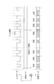
- FIG. 1 is a diagram illustrating a configuration example of a first embodiment of a demodulation device according to the present invention.
- FIG. 2 is a diagram illustrating an example of spread spectrum processing performed by the communication device on the transmission side.
- FIG. 3 is a diagram illustrating a configuration example of the correlation power extraction unit.
- FIG. 4 is a diagram illustrating an operation example of the correlation power extraction unit.
- FIG. 5 is a diagram illustrating an operation example of the correlation power extraction unit.
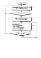
- FIG. 6 is a flowchart illustrating an example of the demodulation process.
- FIG. 7 is a diagram illustrating a modified example of the correlation power extraction unit.
- FIG. 8 is a diagram illustrating a configuration example of a time-division moving average filter.
- FIG. 9 is a diagram illustrating a configuration example of the time-division cyclic addition unit.
- FIG. 10 is a diagram for explaining the operation of the code phase detector.
- FIG. 1 is a diagram illustrating a configuration example of a first embodiment of a demodulation device according to the present invention.
- the demodulator includes a quadrature detection unit 10, a carrier NCO (Numerically Control Oscillator) unit 20, correlation power extraction units 30, 31, and 32, a code phase detection unit 33, a code generation unit 34, Clock generation unit 40, data latch unit 41, carrier frequency deviation detection unit 50, carrier phase detection unit 60, data determination unit 61, demodulation processing control unit 80, multipliers 101, 102, 103, flip-flop And 104, 105.
- a quadrature detection unit 10 a carrier NCO (Numerically Control Oscillator) unit 20
- correlation power extraction units 30, 31, and 32 a code phase detection unit 33
- a code generation unit 34 Clock generation unit 40
- data latch unit 41 data latch unit 41
- carrier frequency deviation detection unit 50 carrier phase detection unit 60
- data determination unit 61 data determination unit 61
- demodulation processing control unit 80 multipliers 101, 102
- the demodulating device shown in FIG. 1 demodulates a spread spectrum signal in a receiver that constitutes a communication device of a spread spectrum communication system.
- the demodulating apparatus has spreading code synchronization, carrier frequency synchronization, bit synchronization even if the spreading code period and the bit period (bit data period) are non-integer multiples.
- carrier phase synchronization is realized, and as a result, data demodulation is performed with good bit error rate characteristics.
- FIG. 2 is a diagram illustrating an example of spread spectrum processing performed by the communication device on the transmission side.
- the spreading code also called PN (Pseudo Random) code
- PN Pseudo Random
- the spread code data ⁇ inversion, normal rotation ⁇ is repeated in the unit of the bit period in the data after the spread spectrum regardless of the spread code period.
- the demodulating device of the present embodiment can demodulate the spread data shown in FIG. 2 alone without using other synchronization signals such as pilot signals.
- the demodulator of the present embodiment can easily realize variable bit rate.
- the configurations of the correlation power extraction units 30 and 32 and the operation of each component are the same as those of the correlation power extraction unit 31. Therefore, the description of the configuration of the correlation power extraction units 30 and 32 and the operation of each component will be omitted.
- the correlation power extraction unit 31 is a unit that is the core of the demodulation process. With this unit, the received signal and the spread code replica (code generation unit) even if the bit data cycle and the spread code cycle are in a non-integer multiple relationship. The cross-correlation power with respect to the spreading code generated by 34 can be extracted.
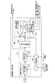
- FIG. 3 is a diagram illustrating a configuration example of the correlation power extraction unit 31.
- the correlation power extraction unit 31 includes a band variable filter 310 including an integral discharge filter 301 and a moving average filter 302, a filter control unit 320, a power conversion unit 330, an adder 341, A cyclic addition unit 340 including a shift register 342 and a multiplier 343 and a maximum value detection / average level measurement unit 350 are provided.
- the spread code replica generated by the code generation unit 34 is multiplied by the reception data via the flip-flop 105 as shown in FIG. Further, it is assumed that the reception data is converted from the intermediate frequency to the baseband frequency by the orthogonal detection unit 10 before being multiplied by the spreading code. That is, the reception data output from the quadrature detection unit 10 is expressed by complex numbers of I and Q. Although not shown in the figure, it is assumed that the conversion (sampling) from analog to digital is performed before the quadrature detection unit 10 or immediately after the quadrature detection unit 10.
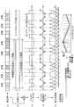
- the data input to the correlation power extraction unit 31 includes a delimiter of the spread code of the received data and a delimiter of the spread code replica generated by the code generation unit 34. 4 (that is, when spreading code synchronization is established) and when the carrier frequency deviation is completely removed (that is, when carrier frequency synchronization is established), FIG. Bit data is restored as shown in FIG. FIG. 4C shows data input to the correlation power extraction unit 31, that is, input data to the band variable filter 310.
- whether or not the spreading code and the carrier frequency are synchronized may be detected by detecting whether or not the bit data shown in FIGS. 4C and 5C is restored.
- Gaussian noise dominates and is added to the received signal. Therefore, the presence / absence of restoration of bit data cannot be determined at the stage of FIGS. 4C and 5C because there are too many noise components.
- correlation power extraction unit 31 performs the filter processing, power addition processing, and maximum value detection processing described below, and the received signal and the spread code replica generated by code generation unit 34 The noise component is removed by extracting the cross-correlation power.
- the band variable filter 310 When the correlation power extraction unit 31 extracts the cross-correlation power, the band variable filter 310 first removes the out-of-band noise component by limiting the received signal with a bandwidth corresponding to the bit rate.
- the variable band filter 310 includes an integral discharge filter 301 and a moving average filter 302.
- the moving average filter 302 may be used.
- the time width for moving average by the moving average filter 302 that is, the number of moving average stages may be set in accordance with the bit period of the received signal.
- variable bandwidth that is, variable bit rate
- the filter control unit 320 based on the bit rate information of the received signal and the sampling rate information of the input data. It should be noted that such control is not necessary when the bit rate is not variable.
- FIG. 4 (d) shows a waveform after moving average of the restored bit data (FIG. 4 (c)), which is input data, under the condition that the spreading code and the carrier frequency are synchronized.
- the moving average is performed for each of the I channel and the Q channel.
- the signal waveform after the moving average is a triangular waveform, and if each data indicated by a circle in FIG. 4D can be sampled by the bit clock, the highest S / N ratio is obtained. A signal is obtained.
- a good bit error rate characteristic can be obtained by phase detection of the sampled high S / N signal.
- Each data indicated by a circle corresponds to a cross-correlation value between the received signal obtained with the time width of the bit period and the spread code replica generated by the code generation unit 34.
- the correlation power extraction unit 31 specifies the position of each data indicated by a circle, and outputs information obtained by power integrating each data indicated by a circle, that is, cross-correlation data obtained at a bit period. To do.
- the noise component is input to the correlation power extraction unit 31, so the noise component is The output of the band-variable filter 310 after the moving average is not obtained with a high amplitude, and a disordered low-amplitude waveform is output.
- the triangular waveform shown in FIG. 4 (d) is doubled as shown in FIG. 4 (e) because the negative amplitude is folded back to the positive side. It is converted into a power data series having frequency components.
- the cyclic addition unit 340 cyclically adds the power data output from the power conversion unit 330 in a bit cycle.
- the number of stages of the shift register 342 in the cyclic addition unit 340 is set by the filter control unit 320, and is set to the same value as the number of moving average stages in the preceding moving average filter 302.
- the number of stages of the moving average filter 302 and the number of stages of the shift register 342 in the cyclic adder 340 are both set to 1022.
- the bit period of the received data corresponds to the average time width of 32 stages of the moving average filter 302
- the number of stages of the moving average filter 302 and the number of stages of the shift register 342 in the cyclic adder 340 are both set to 32 stages.
- the moving average stage number is set in accordance with the bit period, but the number of shift register stages in the cyclic adder 340 is eventually set in accordance with the bit period.
- the number of moving average stages and the number of shift register stages in the cyclic adder 340 are variably set according to a plurality of bit periods (for example, ⁇ 32 Stage, 1022 stage ⁇ ).
- the sampling rate of the data input to the correlation power extraction unit 31 is several hundred times higher than the bit rate (for example, 1022 stages as described above) Then, the processing after the moving average filter 302 in the correlation power extraction unit 31 is oversampling high with respect to the bit rate, the power consumption increases, and the number of stages of each shift register of the moving average filter 302 and the cyclic addition unit 340 Incurs an increase.
- an integral discharge filter 301 shown in FIG. 3 is installed in front of the moving average filter 302 as a countermeasure.
- the integral discharge filter 301 will be described.
- the integral discharge filter 301 repeats the operation of integrating and outputting D pieces of continuously input data, where D is the number of stages.
- D is the number of stages.
- the integration result is output, the integration value is cleared (discharged), and the next consecutively input data are integrated. Thereafter, the same processing is repeated.
- this processing it is possible to reduce noise components included in the input data and to reduce the data sampling rate. That is, the data sampling rate of the data output from the integral discharge filter 301 can be reduced to 1 / D times the sampling rate of the input data.
- the number of stages of each shift register of the moving average filter 302 and the cyclic addition unit 340 is as follows in the configuration without the integral discharge filter 301. 320 stages are required, and the operation speed is 320 times the bit rate.
- the circuit scale and power consumption can be reduced.
- the design is such that the number of stages D of the integral discharge filter 301 can be set in three ways: ⁇ 2 stages, 8 stages, 64 stages ⁇ , and the moving average filter 302 and cyclic addition
- the filter control unit 320 performs such setting of the number of stages.
- the filter control unit 320 acquires the sampling rate information of the input data and the bit rate information of the received data from the demodulation processing control unit 80 (see FIG. 1), and the number of stages of the integral discharge filter 301 from the acquired two pieces of information. And the number of stages of each shift register of the moving average filter 302 and the cyclic adder 340 are determined and set in these units.
- bit rate information and the sampling rate information of the input data input from the demodulation processing control unit 80 to the filter control unit 320 are given to the demodulation processing control unit 80 from the host system (for example, CPU) before starting communication.
- the data output from the shift register 342 is multiplied by the forgetting factor ⁇ by the multiplier 343, and then the input data from the next power converter 330 and the adder It is added at 341.
- the added data is input to the shift register 342 again.
- the time constant of the cyclic adder 340 is determined by the forgetting factor ⁇ (0 ⁇ ⁇ 1). The larger the value of ⁇ , the higher the time constant and the noise resistance. However, as the value of ⁇ increases, the tracking performance with respect to the bit phase shift is impaired. Therefore, the value of ⁇ is appropriately set according to the system to be applied.
- the values C 0 to C 7 in the shift register 342 after four round additions are expressed by the following equations (1) to (8).
- C 0 R 0 ⁇ ⁇ 3 + R 8 ⁇ ⁇ 2 + R 16 ⁇ ⁇ + R 24 (1)
- C 1 R 1 ⁇ ⁇ 3 + R 9 ⁇ ⁇ 2 + R 17 ⁇ ⁇ + R 25 (2)
- C 2 R 2 ⁇ ⁇ 3 + R 10 ⁇ ⁇ 2 + R 18 ⁇ ⁇ + R 26 (3)
- C 3 R 3 ⁇ ⁇ 3 + R 11 ⁇ ⁇ 2 + R 19 ⁇ ⁇ + R 27 (4)
- C 4 R 4 ⁇ ⁇ 3 + R 12 ⁇ ⁇ 2 + R 20 ⁇ ⁇ + R 28 (5)
- C 5 R 5 ⁇ ⁇ 3 + R 13 ⁇ ⁇ 2 + R 21 ⁇ ⁇ + R 29 (6)
- C 6 R 6 ⁇ ⁇ 3 + R 14 ⁇ ⁇ 2 + R 22 ⁇ ⁇ + R 30 (7)
- C 7 R 7 ⁇ ⁇ 3 + R 15 ⁇ ⁇ 2 + R 23 ⁇ ⁇ + R 31 (8)
- the result when the time of 16 bits has elapsed after the cyclic addition of the power data of FIG. 4E at the illustrated cyclic addition timing is shown in FIG.
- the power data in FIG. 4 (e) under the condition that the spreading code and the carrier frequency are synchronized, if the transition of the bit data is random, the behavior is a triangular wave, and if there is no transition, the behavior is DC.
- the peak position of the triangular wave shown in FIG. 4 (e) has a relationship that coincides with the timing of data indicated by the circles in FIG. 4 (d). Therefore, when the power data of FIG.
- the "maximum value” data is indicated by black circles ( ⁇ ).
- This maximum value data is correlation power obtained by power integrating the cross-correlation value between the received signal obtained in the time width of the bit period and the spread code replica generated by the code generation unit 34.
- the maximum value ( ⁇ ) shows a large value under the condition that the spreading code and the carrier are synchronized.
- the maximum value ( ⁇ ) behaves as a small value as shown in FIG.
- the detected maximum value is output as the correlation peak power (P)
- FIG. 4 shows an example of operation when bit transitions occur randomly.
- the position (CT) indicating the maximum value indicates a random value, but the correlation average power (AP) rises to a level equivalent to the correlation peak power (P) at the time of data transition.
- the average level measurement unit 350 selects one of C n as the maximum value, a desired correlation peak power (P) can be obtained.
- the correlation peak power (P) is lowered.
- P correlation peak power
- FIG. 5 when spreading code synchronization is lost, bit data is not restored even if the received data is multiplied by the spreading code (see FIG. 5C).
- the output of the variable band filter 310 that averages the received data multiplied by the spreading code also changes irregularly at a small level as shown in FIG.
- the correlation peak power (P) and the correlation average power (AP), which are the maximum values thereof, show small values.
- the correlation peak power (P) and the correlation average power (AP) are small values even when the carrier frequency is shifted by a bit rate or more and the carrier is asynchronous.
- the correlation peak power (P) and correlation average power (AP) obtained by the correlation power extraction unit 31 are omitted in FIG. 1, but are input to the demodulation processing control unit 80 to receive a desired signal. It is used to determine whether or not code synchronization / carrier synchronization is possible.
- the correlation power extraction unit 31 performs correlation power by band limitation, correlation power cyclic addition of the bit period, and maximum value detection processing.
- the correlation peak power (P) and the correlation average power (AP) output from the extraction unit 31 show large values.
- both the correlation peak power (P) and the correlation average power (AP) output from the correlation power extraction unit 31 are small values.
- each synchronization (spreading code timing synchronization, carrier frequency synchronization) even in a state where the spreading code timing and the carrier frequency deviation are unknown. )
- each synchronization spreading code timing synchronization, carrier frequency synchronization
- FIG. 6 is a flowchart illustrating an example of demodulation processing executed by the demodulation device according to the present embodiment.
- the demodulation processing control unit 80 sends a periodic spreading code replica shift command to the code generation unit 34 and also sends a periodic local frequency shift command to the carrier NCO unit 20.
- the code shift range is set to include the length of one spread code
- the local frequency shift range is set to include the assumed maximum carrier frequency deviation.
- the code generation unit 34 Upon receiving the shift instruction, the code generation unit 34 periodically changes (shifts) the timing of the spreading code (spreading code replica) output to the multiplier 103 and the flip-flop 105, and the carrier NCO unit 20 The frequency of the local signal (cos, sin signal) clock output to the quadrature detection unit 10 is periodically shifted.
- the demodulation processing control unit 80 controls the code generation unit 34 and the carrier NCO unit 20 so that no shift occurs at the same time.
- the carrier NCO unit 20 sets the frequency of the local signal (hereinafter referred to as a local frequency) within a specified range (within the range of local frequency shift). Shift periodically with a certain step width.
- the code generation unit 34 shifts the output timing of the spread code by one sample.
- the carrier NCO unit 20 moves within the specified range in the same manner as described above. Shift local frequency periodically. Thereafter, by repeating the same procedure, the code generation unit 34 periodically shifts the output timing of the spread code within the specified range (within the code shift range).
- the demodulation processing control unit 80 extracts a plurality of correlation peak powers (P k ) and correlation average powers (AP k ) obtained while two-dimensionally changing the spreading code timing and the local frequency. Obtained from the unit 31.
- the demodulation processing control unit 80 extracts the maximum correlation peak power P k from the plurality of correlation peak powers (P k ) obtained two-dimensionally by the correlation power extraction unit 31, and further determines the reliability of the correlation peak power P k.
- the extracted correlation peak power P k is compared with a certain constant ⁇ (threshold value) (step S2).
- step S2 When the correlation peak power P k satisfies the following equation (10) (step S2: Yes), the demodulation processing control unit 80 determines that the signal reception is normal and the correlation peak power P k is obtained.
- the timing and local frequency are set in the code generation unit 34 and the carrier NCO unit 20, respectively (step S3).
- the code generation unit 34 starts spreading code output at the set spreading code timing, and the carrier NCO unit 20 starts generating a local signal of the set frequency.
- the reliability may be confirmed by comparing the correlation average power AP k with a certain constant ⁇ ′.
- AP k > ⁇ ′ (10a)
- the demodulation processing control unit 80 can detect the reception of the all-zero pattern and the other (random pattern, 0101 pattern) reception by the following equation.
- ⁇ is a constant (threshold value). P k ⁇ AP k ⁇ ⁇ (when all-zero pattern is received) (10b) P k > AP k ⁇ ⁇ (when receiving a random pattern, 0101 pattern) (10c)
- pattern detections are conditional on satisfying Expression (10) or Expression (10a), and are invalid if not satisfied.
- Such pattern detection information is useful for grasping the state of carrier synchronization or bit synchronization by the demodulator alone. For example, bit synchronization cannot be established unless a random pattern or 0101 pattern is received, but this bit synchronization can be detected based on whether or not the above equation (10c) is established.
- step S2 when the expression (10) is not satisfied (step S2: No), it is determined that the signal is not received in a normal state such as signal disconnection, and the condition (code timing setting) in which the correlation peak power P k is obtained. It is determined that the reliability of the combination of the value and the local frequency setting value is low, and the above initial synchronization processing is repeated again.
- a ⁇ b code shift number (a) ⁇ local frequency shift number (b)
- a ⁇ b ⁇ J [bit] (where J is the cycle of the bit period) It takes a long time. Therefore, a plurality of correlation power extraction units may be provided in parallel and the time may be reduced by performing parallel processing.
- the time required for the initial synchronization can be reduced from a ⁇ b ⁇ J [bit] to (a ⁇ b ⁇ J) / 3 [bit].
- the spreading code output from the code generation unit 34 is delayed by one sample by the flip-flops 104 and 105 and given to each correlation power extraction unit (30, 31, 32).
- the search on the shift number (a) side is reduced to 1/3 times.
- the correlation peak power (P ⁇ 1 , P 0 , P +1 ) output from each correlation power extraction unit is connected to the code phase detection unit 33, which will be described later.
- the initial synchronization process shown in step S1 of FIG. 6 no signal flows in this connection.
- the connection relationship is not shown in FIG. 1, but the correlation peak power (P k ) and the correlation average power (AP k ) obtained by each correlation power extraction unit (30, 31, 32) are Are connected (input) to the demodulation processing control unit 80.
- the demodulation processing control unit 80 controls the three correlation power extraction units (30, 31, 32), and the correlation peak power (P) output simultaneously by each correlation power extraction unit (30, 31, 32).
- correlation mean power (AP) was collected and, based on the collected results, it performs the signal detection of the formula (10), a set of code timing and the local frequency showing the correlation peak power P x.
- the number of correlation power extraction units is not necessarily three, and may be further increased.
- the circuit scale increases by the increased amount, but the time required for the initial synchronization can be reduced.
- the correlation power extraction unit is operated in a time-sharing manner other than the integral discharge filter, so that an arithmetic circuit such as an adder can be shared and the circuit scale can be reduced.
- the circuit shown in FIG. 7 includes a variable bandwidth filter 310, a cyclic addition unit 340, and a maximum value detection / average level measurement unit 350 of the correlation power extraction unit 31 shown in FIG. This corresponds to a replacement with the cyclic addition unit 370 and the maximum value detection / average level measurement unit 380.
- the time division type variable band filter 360 includes integral discharge filters 301a to 301e, a parallel / serial converter 361, and a time division moving average filter 362.
- the integral discharge filters 301a to 301e are the same as the integral discharge filter 301 shown in FIG.
- the parallel-serial converter 361 rearranges the data output in parallel from the integral discharge filters 301a to 301e into serial data.
- FIG. 7 shows a configuration in a case where a circuit equivalent to a circuit in which five circuits corresponding to the correlation power extraction unit 31 shown in FIG. 3 are arranged in parallel is realized in a time division manner.
- the output terminals of the integral discharge filters 301a, 301b, 301c, 301d, and 301e have a bit rate reduced to 16 times, for example. Therefore, even if these data are parallel-serial converted and 5-time division multiplexed by the parallel-serial converter 361, The operating speed is 80 times the bit rate. With this speed, there is little possibility of exceeding the upper limit of the device operating speed.
- the multiplexing number is not limited to five, and multiplexing may be performed within a range that does not exceed the upper limit of the operation speed of the device.
- the time-division moving average filter 362 that realizes five time divisions is configured as shown in FIG. 8, for example.
- the time-division moving average filter 362 includes 5-stage shift registers (5D) 401 to 404 and adders 405 to 407.
- 5D 5-stage shift registers
- adders 405, 406, and 407 add the respective outputs, so that five data from data # (-2) to data # (+ 2) are added.
- the moving average result corresponding to can be obtained by time division. Since the baseband signal is actually handled, two filters shown in FIG. 8 are required for Ich and Qch.
- the data output in a time division manner from the time division moving average filter 362 is converted into power data by the power conversion unit 330 and then input to the time division type cyclic addition unit 370.
- the time division type cyclic addition unit 370 is configured as shown in FIG. 9, for example. As illustrated, the time-division cyclic adder 370 includes five-stage shift registers (5D) 411 to 414, a multiplier 415, and an adder 416. As shown in the figure, the time-division type cyclic addition unit 370 converts the data input in five time divisions into a register in which a plurality of five-stage shift registers (5-stage shift registers 411, 412, 413, 414) are connected in series. input. The output of the final five-stage shift register 414 is added to the input data by the adder 416 while being multiplied by the forgetting factor ⁇ by the multiplier 415, thereby forming an integration loop.
- 5D five-stage shift registers
- the maximum value detection / average level measurement unit 380 monitors the output of each five-stage shift register (five-stage shift registers 411, 412, 413, 414), so that data # (-2) to data # (+ 2)
- the register value C n of five data can be monitored in a time division manner. Similar to the maximum value detection / average level measurement unit 350, the maximum value detection / average level measurement unit 380 detects the maximum value in C n . Then, the detected maximum value is output as the correlation peak power (P), and the correlation data timing information (CT) indicating the position of the maximum value and the average value (AP) of C n are output.
- P correlation peak power
- CT correlation data timing information
- the demodulation processing control unit 80 determines that the condition described in step S2, that is, the above equation (10) is satisfied, and notifies the code generation unit 34 of the spreading code timing when the correlation peak power P x is obtained.
- the synchronization tracking process shown in step S4 is executed. Specifically, the processes of “(1) code phase synchronization”, “(2) bit synchronization”, “(3) carrier frequency synchronization”, and “(4) carrier phase synchronization” are executed. Hereinafter, these processes will be described.
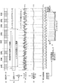
- the code phase detection unit 33 detects a code phase error from the output values (P ⁇ 1 , P 0 , P +1 ) of each correlation power extraction unit (correlation power extraction unit 30, 31, 32). Then, feedback control for canceling the phase error is periodically performed on the code generator 34.
- the spreading code given to the multipliers 101 to 103 before the three correlation power extraction units 30 to 32 is multiplied by the multiplier 101 by +1/2 chip delay, the multiplier 102 by +0 chip delay, and multiplication.
- the instrument 103 provides +1/2 chip advance.
- the initial code timing control is already performed after satisfying the equation (10), if there is no influence of noise after this control, it is output from the correlation power extraction unit 31.
- the code timing control is not ideally performed due to the influence of noise or the like, for example, as shown in FIG. 10, the power of the correlation power P 0 decreases and the above relationship is lost (P ⁇ 1 ⁇ P + 1 ). Even if ideally controlled, the shift gradually occurs due to the influence of the subsequent Doppler frequency or the like.
- the code phase detection unit 33 detects such an error from the output values (P ⁇ 1 , P 0 , P +1 ) of the correlation power extraction unit (30, 31, 32), and periodically performs feedback control for canceling the phase error. This is given to the code generator 34.
- the code phase error ⁇ is obtained by, for example, quadratic interpolation of three correlation powers (P ⁇ 1 , P 0 , P +1 ), and the peak point of the correlation characteristics (marked by ⁇ in FIG. 10) And a timing error from the center point of the chip timing (position of P 0 ) to the specified peak point may be obtained.
- each correlation power extraction unit is arranged in parallel, and a code for obtaining each correlation power
- the code phase is not limited to 1 ⁇ 2 chip intervals.
- the code phase for obtaining each correlation power may be a 1/4 chip interval, and five may be arranged in parallel.
- N correlation powers are subjected to quadratic interpolation, and the peak point of correlation characteristics (marked with a circle in FIG. 10) is specified.
- the clock generation unit 40 reproduces the bit clock based on the position information of the maximum value output from the correlation power extraction unit 31 (position information where the maximum value of the correlation peak power is obtained),
- the data latch unit 41 latches the data identification point from the output data of the correlation power extraction unit 31 using the clock.
- the data latch unit 41 latches the reception data (data D i after band limitation) extracted by the band variable filter 310 of the correlation power extraction unit 31.
- the clock generation unit 40 starts the operation after the initial control of the spreading code timing and the initial control of the local frequency as shown in the flow of FIG. In this case, the correlation power extraction process shown in FIG. 4 is performed.
- the clock generation unit 40 uses the timing shown in FIG. 4 (f) based on the timing indicating the maximum value of each power after cyclic addition shown in FIG.
- the bit clock that latches the data identification point ( ⁇ mark) after passing through the filter in d) is regenerated.
- the data latch unit 41 uses the regenerated bit clock to latch the data identification point ( ⁇ mark) after passing through the filter of FIG. 4D, so that the subsequent data determination unit 61, the carrier phase detection unit 60, and Output to the carrier frequency deviation detector 50.
- This bit synchronization processing is the same as the processing disclosed in Japanese Patent No. 5094469 (timing reproduction device and reception device
- the carrier frequency deviation detector 50 starts operating when the initial control of the code timing and the initial control of the local frequency are completed.
- the carrier frequency deviation detection unit 50 obtains the reception phase indicated by the data identification point latched by the data latch unit 41 described above, and obtains the residual carrier frequency deviation from the difference value between the preceding and following reception phase data.
- feedback control for canceling the residual carrier frequency deviation is periodically performed on the carrier NCO unit 20.
- the received data is ⁇ 0, ⁇ and phase modulation is repeated randomly.
- the subtraction result indicates one of ⁇ 0, ⁇ .
- the subtraction result indicates one of ⁇ , ⁇ + ⁇ .
- the carrier frequency deviation detection unit 50 degenerates (modulo ⁇ ) in the phase range ⁇ after the 1-bit delay detection with respect to the reception phase data indicated by the data identification point, and averages the result.
- the carrier frequency deviation ⁇ can be extracted.
- the carrier frequency deviation detector 50 can extract the residual carrier frequency deviation ⁇ while removing the BPSK modulation component ⁇ 0, ⁇ .
- the received data is ⁇ 0, ⁇ / 2, ⁇ , ⁇ / 2 ⁇ , and the phase modulation is repeated randomly.
- the processing may be performed in the same manner by changing the processing to modulo ⁇ / 2.
- the carrier frequency deviation detector 50 corrects the spreading code frequency based on the obtained residual carrier frequency deviation ⁇ information. You may go to
- the demodulator according to the present embodiment can establish carrier frequency synchronization.
- This carrier phase offset component is not limited to a fixed value, but gradually changes due to phase noise and the carrier frequency synchronization error.
- the carrier phase detection unit 60 extracts this carrier phase offset component and gives it to the data determination unit 61.
- the data determination unit 61 corrects the vector angle of the data identification point latched by the preceding data latch unit 41 with the carrier offset component as the reference axis.
- the carrier phase offset component can be extracted by performing non-linear processing on the data identification point to remove the modulation component and then averaging.
- a specific extraction method is disclosed in Japanese Patent No. 3498600 (a carrier phase estimation device and a demodulator using the carrier phase estimation device).
- the data determination unit 61 obtains the vector angle of the data identification point D i using the carrier offset component Q i by the following equation (11). Further, the demodulated data ⁇ 0, 1 ⁇ is determined based on the amplitude data A i after vector angle correction.
- a i D i ⁇ exp [ ⁇ jQ i ] (11)
- the demodulator obtains the cross-correlation power of the bit data width by the series of signal processing in the correlation power extraction unit, and realizes the spread code synchronization and the carrier synchronization of the demodulator. .
- the demodulation processing control unit 80 determines whether or not spreading code synchronization and carrier frequency synchronization can be maintained by monitoring the correlation peak power P 0 obtained by the correlation power extraction unit 31. That is, it is monitored whether or not P 0 maintains a state larger than a predetermined threshold (step S5), and if not maintained (step S5: No), it is determined that a synchronization error has occurred. . In this case, the process returns to step S1, and the code generation unit 34 and the carrier NCO unit 20 are controlled so as to execute the process of estimating the spreading code timing and the carrier frequency and the subsequent process.
- step S5 When P 0 can maintain a state larger than the predetermined threshold (step S5: Yes), the code phase detection unit 33, the clock generation unit 40, the carrier so as to continue the synchronization tracking process shown in step S4.
- the frequency deviation detector 50 and the carrier phase detector 60 are controlled.
- These code phase detection unit 33, clock generation unit 40, carrier frequency deviation detection unit 50, carrier phase detection unit 60, and demodulation processing control unit 80 realize synchronization tracking means.
- the demodulating apparatus is configured to perform cross-correlation of the bit data width without performing cross-correlation of the spreading code period, so that the bit data period and the spreading code period have a non-integer multiple relationship. Even in this case, there is no restriction on the demodulation process, and it is possible to prevent the demodulation performance (synchronization performance) from deteriorating.
- the demodulator according to the present embodiment does not use a pilot signal separately for the synchronization of the demodulator, a good bit error rate characteristic can be realized with a small transmission power in which the pilot signal is not multiplexed.
- the flow shown in FIG. 6 has been described, but it is not always necessary to follow this flow.
- the processes of steps S1 and S2 in FIG. 6 are not performed, and instead, initial code timing synchronization and initial local frequency synchronization may be performed using pilot signals.
- the present embodiment may be applied only to the synchronization tracking process shown in step S4. That is, the correlation peak power (P x ) obtained by each correlation power extraction unit, the position (CT) where the correlation peak power was obtained, and the correlation average power (AP x ) may be used only in the synchronization tracking process. .
- Embodiment 2 FIG. In the first embodiment, it has been shown that data demodulation is realized and the bit rate is variable even when the bit period and the spreading code period are non-integer multiples.
- the sampling rate of the input data is 331.127 times the bit rate and the sampling rate with respect to the bit rate is a non-integer multiple
- D 20
- the clock frequency deviation corresponding to the ratio is obtained. Occurs after integral discharge filter processing. This leads to deterioration of synchronization characteristics and bit error rate characteristics.
- the stage number D of the integral discharge filter 301 is not fixedly set to either 16 or 17, It is dynamically controlled by the filter control unit 320.
- D ⁇ ⁇ 20, 21 ⁇ is dynamically switched at a certain frequency so that the sampling rate after the output of the integral discharge filter 301 is reached. Is set to 16 times the average bit rate. Specifically, the number of stages D of the integral discharge filter 301 and its switching frequency are obtained by the following calculation.
- the sampling rate of the data before the integral discharge filter is Fs and the bit rate is Rb
- the stage number D of the integrated discharge filter may be set to Ovs / Ots, but D is not always an integer. Absent.
- the demodulator of the second embodiment has a control for dynamically switching the number of stages of the integral discharge filter even when the sampling rate with respect to the bit rate is a non-integer multiple in addition to the effects shown in the first embodiment.
- good characteristics can be realized by adding a small circuit that only adds.
- the dynamic control of the number of integrated discharge filter stages shown in the second embodiment can be widely applied if the sampling rate with respect to the bit rate is a non-integer multiple condition, and the bit data period and the spreading code period are non-integer multiples.
- the present invention can be applied not only to a system but also to a communication system in which both are integral multiples and a communication system using a pilot for synchronization.
- the example of the dynamic control of the integral discharge filter is shown based on the formula (14). However, it is not necessarily based on the formula (14). Any expression may be used as long as the control for dynamically switching the two stages so as to substantially match the desired number of oversamples is realized.
- the demodulator according to the present invention is useful as a demodulator that constitutes a communication device on the receiving side of a spread spectrum communication system.
Landscapes
- Engineering & Computer Science (AREA)
- Computer Networks & Wireless Communication (AREA)
- Signal Processing (AREA)
- Synchronisation In Digital Transmission Systems (AREA)
Abstract
Description
図1は、本発明にかかる復調装置の実施の形態1の構成例を示す図である。図示したように、復調装置は、直交検波部10と、キャリアNCO(Numerically Control Oscillator)部20と、相関電力抽出部30,31,32と、コード位相検出部33と、コード生成部34と、クロック生成部40と、データラッチ部41と、キャリア周波数偏差検出部50と、キャリア位相検出部60と、データ判定部61と、復調処理制御部80と、乗算器101,102,103と、フリップフロップ104,105と、を備えて構成されている。
C0=R0×α3+R8×α2+R16×α+R24 …(1)
C1=R1×α3+R9×α2+R17×α+R25 …(2)
C2=R2×α3+R10×α2+R18×α+R26 …(3)
C3=R3×α3+R11×α2+R19×α+R27 …(4)
C4=R4×α3+R12×α2+R20×α+R28 …(5)
C5=R5×α3+R13×α2+R21×α+R29 …(6)
C6=R6×α3+R14×α2+R22×α+R30 …(7)
C7=R7×α3+R15×α2+R23×α+R31 …(8)

Pk>β …(10)
APk>β’ …(10a)
Pk≦APk×γ (オールゼロパターン受信時) …(10b)
Pk>APk×γ (ランダムパターン、0101パターン受信時) …(10c)
コード位相検出部33は、各相関電力抽出部(相関電力抽出部30,31,32)の出力値(P-1,P0,P+1)からコード位相誤差を検出し、位相誤差を打ち消すフィードバック制御をコード生成部34に対して周期的に行う。
クロック生成部40は、相関電力抽出部31から出力された最大値の位置情報(相関ピーク電力の最大値が得られる位置の情報)を元に、ビットクロックを再生し、本クロックを用いて相関電力抽出部31の出力データからデータ識別点をデータラッチ部41がラッチする。
キャリア周波数偏差検出部50は、前記のコードタイミングの初期制御、ローカル周波数の初期制御が終了すると動作を開始する。
上記のキャリア周波数同期が確立すると、キャリア位相オフセット成分のみが残留する。このキャリア位相オフセット成分は固定値とは限らず、位相雑音や前記キャリア周波数同期誤差によって、緩やかに変化する。
Ai=Di×exp[-jQi] …(11)
実施の形態1では、ビット周期と拡散コード周期が非整数倍の関係でもデータ復調を実現し、かつビットレート可変も実現することを示した。
DINT+1>D≧DINT …(12)
{(DINT+1)b+(DINT)a}/(a+b)=D …(13)
{(DINT+1)b+(DINT)a}=D×(a+b)
(DINT-D)a=(D-DINT-1)b
a=(D-DINT-1)b/(DINT-D) …(14)
Claims (8)
- スペクトラム拡散された受信データを復調する復調装置であって、
逆拡散後の受信データから雑音成分を除去するフィルタ手段と、
雑音成分除去後の受信データの各サンプル値を電力値に変換する電力変換手段と、
前記電力値を受信データのビット周期で巡回加算する巡回加算手段と、
前記巡回加算手段による巡回加算結果から最大値を検出する最大値検出手段と、
前記最大値検出手段が検出した最大値情報に基づいて拡散コードタイミングおよびキャリア周波数を推定する推定手段と、
前記推定手段による拡散コードタイミングの推定結果に従って拡散コードを生成する拡散コード生成手段と、
前記推定手段によるキャリア周波数の推定結果に従ってローカル信号の周波数を設定するローカル信号生成手段と、
を備えることを特徴とする復調装置。 - 前記フィルタ手段は、逆拡散後の受信データを移動平均することを特徴とする請求項1に記載の復調装置。
- 前記フィルタ手段は、受信データのビットレートに応じた時間幅で移動平均を実施することを特徴とする請求項2に記載の復調装置。
- 前記フィルタ手段は、
逆拡散後の受信データを一定の時間区間ごとに積分する積分フィルタと、
前記積分放電フィルタから出力された積分値を移動平均する移動平均フィルタと、
を備えることを特徴とする請求項1に記載の復調装置。 - 前記逆拡散後の受信データのサンプリングレートおよびビットレートに基づいて、前記時間区間および前記移動平均を実施する時間幅を制御するフィルタ制御手段、
をさらに備えることを特徴とする請求項4に記載の復調装置。 - 前記サンプリングレートが前記ビットレートの非整数倍の場合、
前記フィルタ制御手段は、前記サンプリングレートを前記ビットレートで除した結果に基づいて決定したタイミングで前記時間区間を周期的に切り替えることを特徴とする請求項5に記載の復調装置。 - 前記拡散コードタイミングと前記ローカル信号の周波数をそれぞれ規定されている範囲で、一定のステップ幅でシフトさせる復調処理制御手段、
を備えることを特徴とする請求項1から6のいずれか一つに記載の復調装置。 - 前記巡回加算手段による巡回加算結果に基づいて、拡散コードの位相同期制御、受信データのビット同期制御、キャリア周波数の同期制御およびキャリア位相の同期制御を行う同期追尾手段、
を備えることを特徴とする請求項1から6のいずれか一つに記載の復調装置。
Priority Applications (6)
| Application Number | Priority Date | Filing Date | Title |
|---|---|---|---|
| CA2949026A CA2949026C (en) | 2014-05-15 | 2014-05-15 | Demodulation apparatus |
| JP2016519052A JP6242481B2 (ja) | 2014-05-15 | 2014-05-15 | 復調装置 |
| EP14891839.4A EP3145091B1 (en) | 2014-05-15 | 2014-05-15 | Demodulation apparatus |
| US15/310,317 US9923596B2 (en) | 2014-05-15 | 2014-05-15 | Demodulation apparatus |
| PCT/JP2014/062971 WO2015173928A1 (ja) | 2014-05-15 | 2014-05-15 | 復調装置 |
| ES14891839T ES2716677T3 (es) | 2014-05-15 | 2014-05-15 | Aparato de demodulación |
Applications Claiming Priority (1)
| Application Number | Priority Date | Filing Date | Title |
|---|---|---|---|
| PCT/JP2014/062971 WO2015173928A1 (ja) | 2014-05-15 | 2014-05-15 | 復調装置 |
Publications (1)
| Publication Number | Publication Date |
|---|---|
| WO2015173928A1 true WO2015173928A1 (ja) | 2015-11-19 |
Family
ID=54479497
Family Applications (1)
| Application Number | Title | Priority Date | Filing Date |
|---|---|---|---|
| PCT/JP2014/062971 Ceased WO2015173928A1 (ja) | 2014-05-15 | 2014-05-15 | 復調装置 |
Country Status (6)
| Country | Link |
|---|---|
| US (1) | US9923596B2 (ja) |
| EP (1) | EP3145091B1 (ja) |
| JP (1) | JP6242481B2 (ja) |
| CA (1) | CA2949026C (ja) |
| ES (1) | ES2716677T3 (ja) |
| WO (1) | WO2015173928A1 (ja) |
Cited By (1)
| Publication number | Priority date | Publication date | Assignee | Title |
|---|---|---|---|---|
| US10432251B2 (en) | 2016-03-28 | 2019-10-01 | Mitsubishi Electric Corporation | Receiver, transmitter, radio communication system, and radio communication method |
Families Citing this family (2)
| Publication number | Priority date | Publication date | Assignee | Title |
|---|---|---|---|---|
| SG11202106944PA (en) * | 2018-03-05 | 2021-07-29 | Zte Corp | Transmissions using spreading codes |
| CN119815490A (zh) * | 2023-10-09 | 2025-04-11 | 博通集成电路(上海)股份有限公司 | 改善信标接收的方法和设备 |
Citations (3)
| Publication number | Priority date | Publication date | Assignee | Title |
|---|---|---|---|---|
| JPH07140224A (ja) * | 1993-11-16 | 1995-06-02 | Nippondenso Co Ltd | スペクトル拡散信号捕捉装置 |
| JPH10282210A (ja) * | 1997-04-04 | 1998-10-23 | Denso Corp | スペクトル拡散信号捕捉装置 |
| JP2009033702A (ja) * | 2007-07-04 | 2009-02-12 | Mitsubishi Electric Corp | タイミング再生装置および受信装置 |
Family Cites Families (6)
| Publication number | Priority date | Publication date | Assignee | Title |
|---|---|---|---|---|
| JPH05327657A (ja) | 1992-05-20 | 1993-12-10 | Ricoh Co Ltd | データ復号回路 |
| US5579338A (en) * | 1992-06-29 | 1996-11-26 | Mitsubishi Denki Kabushiki Kaisha | Spread spectrum receiver using partial correlations |
| US5867525A (en) * | 1997-06-10 | 1999-02-02 | L-3 Commuications Corporation | Synchronizer and method therefor and communications system incorporating same |
| JP3498600B2 (ja) | 1998-11-09 | 2004-02-16 | 三菱電機株式会社 | キャリア位相推定装置とキャリア位相推定装置を用いた復調器 |
| US6456648B1 (en) * | 2001-10-01 | 2002-09-24 | Interdigital Technology Corporation | Code tracking loop with automatic power normalization |
| US8462875B2 (en) * | 2009-07-20 | 2013-06-11 | Mitsubishi Electric Corporation | Timing regenerating device |
-
2014
- 2014-05-15 WO PCT/JP2014/062971 patent/WO2015173928A1/ja not_active Ceased
- 2014-05-15 US US15/310,317 patent/US9923596B2/en active Active
- 2014-05-15 EP EP14891839.4A patent/EP3145091B1/en active Active
- 2014-05-15 JP JP2016519052A patent/JP6242481B2/ja active Active
- 2014-05-15 CA CA2949026A patent/CA2949026C/en not_active Expired - Fee Related
- 2014-05-15 ES ES14891839T patent/ES2716677T3/es active Active
Patent Citations (3)
| Publication number | Priority date | Publication date | Assignee | Title |
|---|---|---|---|---|
| JPH07140224A (ja) * | 1993-11-16 | 1995-06-02 | Nippondenso Co Ltd | スペクトル拡散信号捕捉装置 |
| JPH10282210A (ja) * | 1997-04-04 | 1998-10-23 | Denso Corp | スペクトル拡散信号捕捉装置 |
| JP2009033702A (ja) * | 2007-07-04 | 2009-02-12 | Mitsubishi Electric Corp | タイミング再生装置および受信装置 |
Non-Patent Citations (1)
| Title |
|---|
| See also references of EP3145091A4 * |
Cited By (1)
| Publication number | Priority date | Publication date | Assignee | Title |
|---|---|---|---|---|
| US10432251B2 (en) | 2016-03-28 | 2019-10-01 | Mitsubishi Electric Corporation | Receiver, transmitter, radio communication system, and radio communication method |
Also Published As
| Publication number | Publication date |
|---|---|
| CA2949026C (en) | 2018-08-21 |
| JP6242481B2 (ja) | 2017-12-06 |
| JPWO2015173928A1 (ja) | 2017-04-20 |
| CA2949026A1 (en) | 2015-11-19 |
| US20170272117A1 (en) | 2017-09-21 |
| EP3145091B1 (en) | 2019-02-20 |
| ES2716677T3 (es) | 2019-06-14 |
| EP3145091A4 (en) | 2017-12-13 |
| US9923596B2 (en) | 2018-03-20 |
| EP3145091A1 (en) | 2017-03-22 |
Similar Documents
| Publication | Publication Date | Title |
|---|---|---|
| Kaddoum et al. | Design of a high-data-rate differential chaos-shift keying system | |
| US8761230B2 (en) | Method and apparatus for continuous phase modulation preamble encoding and decoding | |
| US8774318B2 (en) | Method and apparatus for constant envelope modulation | |
| EP0952678A1 (en) | Digital modulation system using modified orthogonal codes to reduce autocorrelation sidelobes | |
| WO2001028146A1 (en) | Apparatus for and method of adaptive synchronization in a spread spectrum communications receiver | |
| US6674790B1 (en) | System and method employing concatenated spreading sequences to provide data modulated spread signals having increased data rates with extended multi-path delay spread | |
| JP2010200319A (ja) | 特にモバイル装置の通信信号受信機の搬送波周波数シフトを推定するための方法 | |
| US9015220B2 (en) | Correlation device | |
| JP6242481B2 (ja) | 復調装置 | |
| JP3523609B2 (ja) | 符号分割多元接続(cdma)コードタイミング追跡装置 | |
| JP2006060691A (ja) | 同期追従回路 | |
| JP2006157643A (ja) | 無線通信システム、無線通信方法及び通信装置 | |
| US6504883B1 (en) | Synchronous detector | |
| JP5635927B2 (ja) | 通信システム、および通信方法 | |
| JP4406326B2 (ja) | 受信装置及びそれを用いた通信装置 | |
| AU2015221710A1 (en) | Wireless transmission device, wireless reception device, wireless communication system, and wireless communication method | |
| JP5094469B2 (ja) | タイミング再生装置および受信装置 | |
| Poberezhskiy | Novel modulation techniques and circuits for transceivers in body sensor networks | |
| Vali et al. | Analysis of a chaos-based non-coherent delay lock tracking loop | |
| RU2733261C1 (ru) | Многоканальный приемник с когерентным частотно-кодовым разделением каналов для приема квадратурно-модулированных сигналов повышенной структурной скрытности | |
| JP4814754B2 (ja) | 通信装置 | |
| CN100550664C (zh) | 码片级相位调整方法与系统 | |
| JP2000078058A (ja) | マッチドフィルタ出力分析・干渉波制御形cdma通信方式 | |
| JP2015162722A (ja) | スペクトル拡散受信機およびスペクトル拡散送信機 | |
| JP5787846B2 (ja) | 受信装置、スペクトル拡散通信装置および通信システム |
Legal Events
| Date | Code | Title | Description |
|---|---|---|---|
| 121 | Ep: the epo has been informed by wipo that ep was designated in this application |
Ref document number: 14891839 Country of ref document: EP Kind code of ref document: A1 |
|
| ENP | Entry into the national phase |
Ref document number: 2016519052 Country of ref document: JP Kind code of ref document: A |
|
| WWE | Wipo information: entry into national phase |
Ref document number: 15310317 Country of ref document: US |
|
| ENP | Entry into the national phase |
Ref document number: 2949026 Country of ref document: CA |
|
| NENP | Non-entry into the national phase |
Ref country code: DE |
|
| REEP | Request for entry into the european phase |
Ref document number: 2014891839 Country of ref document: EP |
|
| WWE | Wipo information: entry into national phase |
Ref document number: 2014891839 Country of ref document: EP |